WO2019021764A1 - アクチュエータ、およびアクチュエータの製造方法 - Google Patents
アクチュエータ、およびアクチュエータの製造方法 Download PDFInfo
- Publication number
- WO2019021764A1 WO2019021764A1 PCT/JP2018/025218 JP2018025218W WO2019021764A1 WO 2019021764 A1 WO2019021764 A1 WO 2019021764A1 JP 2018025218 W JP2018025218 W JP 2018025218W WO 2019021764 A1 WO2019021764 A1 WO 2019021764A1
- Authority
- WO
- WIPO (PCT)
- Prior art keywords
- coil
- substrate
- base
- magnetic sensor
- actuator
- Prior art date
Links
Images


Classifications
-
- H—ELECTRICITY
- H02—GENERATION; CONVERSION OR DISTRIBUTION OF ELECTRIC POWER
- H02K—DYNAMO-ELECTRIC MACHINES
- H02K3/00—Details of windings
- H02K3/04—Windings characterised by the conductor shape, form or construction, e.g. with bar conductors
- H02K3/26—Windings characterised by the conductor shape, form or construction, e.g. with bar conductors consisting of printed conductors
-
- H—ELECTRICITY
- H02—GENERATION; CONVERSION OR DISTRIBUTION OF ELECTRIC POWER
- H02K—DYNAMO-ELECTRIC MACHINES
- H02K11/00—Structural association of dynamo-electric machines with electric components or with devices for shielding, monitoring or protection
- H02K11/20—Structural association of dynamo-electric machines with electric components or with devices for shielding, monitoring or protection for measuring, monitoring, testing, protecting or switching
- H02K11/21—Devices for sensing speed or position, or actuated thereby
- H02K11/215—Magnetic effect devices, e.g. Hall-effect or magneto-resistive elements
-
- G—PHYSICS
- G03—PHOTOGRAPHY; CINEMATOGRAPHY; ANALOGOUS TECHNIQUES USING WAVES OTHER THAN OPTICAL WAVES; ELECTROGRAPHY; HOLOGRAPHY
- G03B—APPARATUS OR ARRANGEMENTS FOR TAKING PHOTOGRAPHS OR FOR PROJECTING OR VIEWING THEM; APPARATUS OR ARRANGEMENTS EMPLOYING ANALOGOUS TECHNIQUES USING WAVES OTHER THAN OPTICAL WAVES; ACCESSORIES THEREFOR
- G03B5/00—Adjustment of optical system relative to image or object surface other than for focusing
-
- H—ELECTRICITY
- H02—GENERATION; CONVERSION OR DISTRIBUTION OF ELECTRIC POWER
- H02K—DYNAMO-ELECTRIC MACHINES
- H02K1/00—Details of the magnetic circuit
- H02K1/06—Details of the magnetic circuit characterised by the shape, form or construction
- H02K1/12—Stationary parts of the magnetic circuit
- H02K1/18—Means for mounting or fastening magnetic stationary parts on to, or to, the stator structures
-
- H—ELECTRICITY
- H02—GENERATION; CONVERSION OR DISTRIBUTION OF ELECTRIC POWER
- H02K—DYNAMO-ELECTRIC MACHINES
- H02K11/00—Structural association of dynamo-electric machines with electric components or with devices for shielding, monitoring or protection
- H02K11/30—Structural association with control circuits or drive circuits
- H02K11/33—Drive circuits, e.g. power electronics
-
- H—ELECTRICITY
- H02—GENERATION; CONVERSION OR DISTRIBUTION OF ELECTRIC POWER
- H02K—DYNAMO-ELECTRIC MACHINES
- H02K15/00—Methods or apparatus specially adapted for manufacturing, assembling, maintaining or repairing of dynamo-electric machines
- H02K15/04—Methods or apparatus specially adapted for manufacturing, assembling, maintaining or repairing of dynamo-electric machines of windings, prior to mounting into machines
-
- H—ELECTRICITY
- H02—GENERATION; CONVERSION OR DISTRIBUTION OF ELECTRIC POWER
- H02K—DYNAMO-ELECTRIC MACHINES
- H02K41/00—Propulsion systems in which a rigid body is moved along a path due to dynamo-electric interaction between the body and a magnetic field travelling along the path
- H02K41/02—Linear motors; Sectional motors
- H02K41/03—Synchronous motors; Motors moving step by step; Reluctance motors
- H02K41/031—Synchronous motors; Motors moving step by step; Reluctance motors of the permanent magnet type
- H02K41/033—Synchronous motors; Motors moving step by step; Reluctance motors of the permanent magnet type with armature and magnets on one member, the other member being a flux distributor
-
- H—ELECTRICITY
- H02—GENERATION; CONVERSION OR DISTRIBUTION OF ELECTRIC POWER
- H02K—DYNAMO-ELECTRIC MACHINES
- H02K41/00—Propulsion systems in which a rigid body is moved along a path due to dynamo-electric interaction between the body and a magnetic field travelling along the path
- H02K41/02—Linear motors; Sectional motors
- H02K41/035—DC motors; Unipolar motors
- H02K41/0352—Unipolar motors
- H02K41/0354—Lorentz force motors, e.g. voice coil motors
- H02K41/0356—Lorentz force motors, e.g. voice coil motors moving along a straight path
Definitions
- the present invention relates to an actuator, and more particularly to an actuator that moves one by the interaction of a coil and a magnet.
- Patent Document 1 discloses an actuator including a coil substrate on which a coil is formed, a base substrate to which the coil substrate is bonded, and a magnetic sensor mounted on the base substrate.
- the actuator moves a movable body provided with a magnet by a magnetic field generated by a coil.
- the current flowing through the coil is controlled by, for example, a driver IC connected to the magnetic sensor based on information (signal from the magnetic sensor) obtained from the magnetic sensor. Therefore, when the mounting position of the coil with respect to the magnetic sensor is deviated, the magnetic field detected by the magnetic sensor, the magnetic field generated by the coil, and the like may change from the defined state, and the characteristics of the actuator may vary.
- An object of the present invention is to provide an actuator including a coil substrate, a base substrate, and a magnetic sensor, in which an individual difference in actuator characteristics is suppressed by suppressing a shift in a positional relationship of the coil with respect to the magnetic sensor. .
- the actuator of the present invention is A coil substrate provided with a magnetic sensor and having a coil; A base substrate on which a coil drive circuit is formed; Equipped with The coil substrate is connected to the base substrate through a conductive bonding material.
- the coil substrate on which the magnetic sensor is provided in advance is mounted on the base substrate via the conductive bonding material, when the coil substrate is mounted on the base substrate, the positional relationship between the magnetic sensor and the coil deviates Is hard to occur. Therefore, compared with the case where the magnetic sensor and the coil substrate are mounted on the base substrate, the position of the coil with respect to the magnetic sensor can be hardly shifted from the predetermined position. Therefore, with this configuration, it is possible to suppress the variation in the characteristics of the actuator caused by the displacement of the position of the coil with respect to the magnetic sensor.
- a shield conductor provided on the base substrate may be provided, and the shield conductor may be disposed between the other conductive pattern formed on the base substrate and the magnetic sensor. preferable.
- the shield conductor since the shield conductor is located between the other conductor pattern formed on the base substrate and the magnetic sensor, noise generated from the other conductor pattern is shielded by the shield conductor. Therefore, with this configuration, the influence of noise generated from the base substrate on the magnetic sensor can be suppressed.
- the coil substrate includes a base formed by laminating a plurality of insulating base layers, and the coil is formed of the plurality of insulating base layers. It may be formed including a plurality of coil conductors formed in two or more insulating base layers.
- a coil is formed by including a plurality of coil conductors respectively formed in two or more insulating base layers, a plurality of insulating base layers (specifically, a plurality of coils) in order to suppress a change in characteristics of the coil. It is necessary to laminate conductors) with high positional accuracy.
- the yield rate of the actuator can be increased as compared with the case where the coil substrate and the base substrate are integrally formed. .
- the base material has a mounting surface to be mounted on the base substrate, and the magnet is disposed on the opposite side of the coil substrate from the base substrate, Preferably, the magnetic sensor is disposed closer to the magnet than the mounting surface. According to this configuration, since the distance between the magnetic sensor and the magnet is short as compared with the case where the magnetic sensor is mounted on the mounting surface, the magnetic field detection accuracy of the magnetic sensor with respect to the magnet can be improved.
- the coil drive circuit is connected to the magnetic sensor, and has a driver IC that controls the current flowing to the coil based on a signal from the magnetic sensor. It may be done.
- the wiring length between the driver IC and the capacitor or the wiring length between the capacitor and the ground can be shortened as compared with the case where the capacitor is mounted on the coil substrate. Therefore, the inductance and conductor resistance in the wiring between the driver IC and the capacitor, or the inductance and conductor resistance in the wiring between the capacitor and the ground can be reduced, and the effect of suppressing the voltage fluctuation of the driver IC by the capacitor is enhanced.
- the base substrate may have a flexible portion having flexibility and a connection portion for external connection connected to the flexible portion.
- the connection portion can be easily connected to another substrate or the like by utilizing the flexibility of the flexible portion (in a state where the flexible portion is bent).
- an external force is applied to the connection portion (for example, when another substrate connected to the connection portion moves)
- stress is hardly transmitted to the coil and the magnetic sensor. Therefore, it is possible to suppress the change in the characteristics of the actuator caused by the transfer of stress to the coil and the magnetic sensor.
- the method of manufacturing an actuator according to the present invention A coil substrate provided with a magnetic sensor and having a coil and a substrate; A base substrate on which a coil drive circuit is formed; A magnet that receives a magnetic field generated by the coil; A method of manufacturing an actuator comprising A coil substrate forming step of providing the magnetic sensor on the substrate; A substrate bonding step of connecting the coil substrate to the base substrate through a conductive bonding material after the coil substrate forming step; It is characterized by having.
- the coil substrate forming step may include the step of mounting the magnetic sensor on the base material.
- the base is formed by laminating a plurality of insulating base layers, and the coil substrate forming step includes the plurality of insulating base layers on which the magnetic sensor is mounted. You may include the process of laminating
- an actuator provided with a coil substrate, a base substrate, and a magnetic sensor, by suppressing the deviation of the positional relationship of the coil with respect to the magnetic sensor, it is possible to realize an actuator in which variations in characteristics among individuals are suppressed.
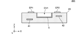
- FIG. 1 is a cross-sectional view of an actuator 301 according to the first embodiment.
- FIG. 2A is a cross-sectional view of the coil substrate 101 according to the first embodiment, and FIG. 2B is a plan view of the coil substrate 101.
- FIG. 3 is a cross-sectional view of the base substrate 201 according to the first embodiment.
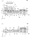
- FIG. 4A is a cross-sectional view of an actuator 302 according to the second embodiment, and FIG. 4B is a cross-sectional view of a base substrate 202 according to the second embodiment.
- FIG. 5A is a cross-sectional view of an actuator 303 according to the third embodiment, and FIG. 5B is a cross-sectional view of a coil substrate 103 according to the third embodiment.
- FIG. 6 is a cross-sectional view of an actuator 304 according to the fourth embodiment.
- FIG. 1 is a cross-sectional view of an actuator 301 according to the first embodiment.
- FIG. 2A is a cross-sectional view of the coil substrate 101 according to the first embodiment
- FIG. 2B is a plan view of the coil substrate 101.
- FIG. 3 is a cross-sectional view of the base substrate 201 according to the first embodiment. The thickness of each part is exaggerated and shown in FIG. 1, FIG. 2 (A), and FIG. The same applies to the cross-sectional views shown later.
- the "actuator" of the present invention is provided with a coil substrate having a coil and a base substrate as described later in detail, and moves a movable body provided with a magnet by a magnetic field generated by the coil.
- the actuator 301 includes a coil substrate 101, a base substrate 201, a magnet 4 and the like.
- the coil substrate 101 has a base 10, a coil L1, connection electrodes P1, P2, P11, P12, a magnetic sensor 1 and the like as shown in FIG. 2 (A) and FIG. 2 (B).
- the base 10 is a substantially rectangular parallelepiped whose longitudinal direction coincides with the X-axis direction, and has a first main surface VS1 and a second main surface VS2 facing each other.
- the base 10 is a laminate formed by laminating a plurality of insulating base layers made of thermoplastic resin.
- the substrate 10 is, for example, a rectangular solid mainly composed of a liquid crystal polymer (LCP) or a polyetheretherketone (PEEK).
- the first main surface VS1 of the base 10 corresponds to the “mounting surface” in the present invention.
- the coil L1 is an approximately four-turn coil formed inside the base 10 and having a winding axis AX along the stacking direction (Z-axis direction) of the plurality of insulating base layers.
- the coil L1 is configured of coil conductors 31 and 32 and an interlayer connection conductor (not shown).
- the coil conductors 31 and 32 are rectangular spiral conductor patterns of about 2 turns formed on different insulating base layers.
- the first end of the coil conductor 31 is connected to the first end of the coil conductor 32 via an interlayer connection conductor (not shown).
- the coil conductors 31 and 32 are conductor patterns, such as Cu foil, for example.
- connection electrodes P1, P2, P11, and P12 are rectangular conductor patterns formed on the first main surface VS1 of the base material 10.
- the connection electrode P1 is connected to the first end of the coil L1 (the second end of the coil conductor 31), and the connection electrode P2 is connected to the second end of the coil L1 (the second end of the coil conductor 32) There is.
- the connection electrodes P1, P2, P11 and P12 are conductor patterns of, for example, Cu foil.
- the magnetic sensor 1 is an element that senses a magnetic field generated when a current flows in the coil L1 or a magnetic field from the outside, and detects the amount of movement of the magnet 4.
- the magnetic sensor 1 is, for example, a Hall element utilizing a Hall effect.
- the magnetic sensor 1 is provided on the first main surface VS1 of the substrate 10. Specifically, the magnetic sensor 1 has terminals P21 and P22 on the mounting surface (the upper surface of the magnetic sensor 1 in FIG. 2A), and these terminals P21 and P22 are connected via the conductive bonding material 3 The connection electrodes P11 and P12 are respectively connected. As shown in FIG. 2A, the magnetic sensor 1 is disposed at a position overlapping the winding axis AX of the coil L1.
- the conductive bonding material 3 is, for example, a solder.
- the base substrate 201 has a base 20, a cavity CV1 formed on the base 20, a shield conductor 5, connection electrodes EP1 and EP2 formed on the base 20, conductor patterns 41 and 42, and the like. On the base substrate 201, a coil drive circuit for driving the coil L1 is formed.
- the base material 20 is a substantially rectangular parallelepiped whose longitudinal direction coincides with the X-axis direction.
- the base 20 is a laminate formed by laminating a plurality of insulating base layers made of thermoplastic resin.
- the substrate 20 is, for example, a substantially rectangular parallelepiped mainly composed of a liquid crystal polymer (LCP) or a polyetheretherketone (PEEK).
- the cavity CV1 is an opening formed inward (in the ⁇ Z direction) from the surface of the substrate 20 (the upper surface of the substrate 20 in FIG. 3).
- the planar shape of the cavity CV1 is a shape that matches the planar shape of the magnetic sensor 1.
- the magnetic sensor 1 is disposed in the cavity CV1.
- the cavity CV1 is formed, for example, by etching the surface side of the substrate 20 with a laser after forming the substrate 20.
- the shield conductor 5 is a box-shaped conductive member without a top surface, and is fitted in the cavity CV1.
- the shield conductor 5 is obtained, for example, by forming a flat plate made of Cu by plastic deformation (forging).
- connection electrodes EP1 and EP2 are rectangular conductor patterns formed on the surface of the substrate 20 (the upper surface of the substrate 20 in FIG. 3).
- the conductor patterns 41 and 42 are conductor patterns formed inside the base material 20.
- the connection electrodes EP1 and EP2 and the conductor patterns 41 and 42 are, for example, conductor patterns such as Cu foil.
- the coil substrate 101 is connected to the base substrate 201 via the conductive bonding material 3.
- the connection electrodes P1 and P2 of the coil substrate 101 are connected to the connection electrodes EP1 and EP2 of the base substrate 201 via the conductive bonding material 3.
- the coil substrate 101 and the base substrate 201 are connected in a state where the magnetic sensor 1 provided on the coil substrate 101 (base material 10) is disposed in the cavity CV1. Ru. Further, as shown in FIG. 1, the shield conductor 5 is disposed between the magnetic sensor 1 and another conductor pattern (conductor patterns 41 and 42) formed on the base substrate 201.
- the magnet 4 is attached to a movable body (not shown).
- the magnet 4 is disposed on the opposite side (+ Z direction) to the base substrate 201 with the coil substrate 101 interposed therebetween.
- the magnet 4 is, for example, a permanent magnet.
- the actuator 301 is used, for example, as follows.
- the magnet 4 is displaced in the planar direction (for example, the X-axis direction) by the magnetic field radiated from the coil L1 (see the white arrow in FIG. 1).
- the magnetic sensor 1 senses a change in magnetic field when the magnet 4 is displaced.
- the actuator 301 according to the present embodiment has the following effects.
- the shield conductor 5 is disposed between the magnetic sensor 1 and another conductor pattern (conductor patterns 41 and 42) formed on the base substrate 201. According to this configuration, noise generated from other conductor patterns is shielded by the shield conductor 5. Therefore, the influence of the noise generated from the base substrate 201 on the magnetic sensor 1 can be suppressed.
- the magnetic sensor 1 is disposed at a position overlapping the winding axis AX of the coil L1.
- the magnetic sensor 1 since the magnetic sensor 1 is disposed on the winding axis AX of the coil L1 less affected by the magnetic field generated from the coil L1, the influence of the magnetic field generated from the coil L1 can be reduced. Therefore, the magnetic field detection accuracy of the magnetic sensor 1 can be enhanced.
- the base material 10 of the coil substrate 101 and the base material 20 of the base substrate 201 are made of the same main component material (liquid crystal polymer).
- the linear expansion coefficients of the base 10 of the coil substrate 101 and the base 20 of the base substrate 201 substantially match. Therefore, the occurrence of warpage due to the difference in linear expansion coefficient between the base material 10 and the base material 20 due to the temperature change when the coil substrate 101 is mounted on the base substrate 201 (or after mounting) is suppressed. Therefore, with this configuration, the bonding failure between the connection electrodes P1 and P2 of the coil substrate 101 and the connection electrodes EP1 and EP2 of the base substrate 201 is suppressed.
- the base material 10 is a laminated body formed by laminating a plurality of insulating base material layers
- the coil L1 is a plurality of coil conductors 31 and 32 formed in two or more insulating base material layers. Is formed.
- the coil L1 is configured to include a plurality of coil conductors 31 and 32 respectively formed on two or more insulating base layers, a plurality of insulating base layers (a plurality of coil conductors) in order to suppress coil characteristics. It is necessary to stack them with high positional accuracy.
- the actuator 301 according to the present embodiment, the coil substrate 101 and the base substrate 201, which require high positional accuracy at the time of stacking, are separate bodies. Therefore, with this configuration, the non-defective rate of the actuator can be increased as compared with the case where the coil substrate and the base substrate are integrally formed (when the coil substrate and the base substrate are formed of one base material).
- the actuator 301 according to the present embodiment is manufactured, for example, by the following process.
- the coil substrate 101 provided with the magnetic sensor 1 on the base material 10 is prepared. Specifically, the coil substrate 101 is manufactured by the following process.
- the plurality of insulating base layers are, for example, thermoplastic resin sheets such as liquid crystal polymer (LCP) or polyetheretherketone (PEEK).
- LCP liquid crystal polymer
- PEEK polyetheretherketone
- the coil conductors 31, 32 and the connection electrodes P1, P2, P11, P12 are formed on the plurality of insulating base layers.
- a metal foil for example, Cu foil
- the metal foil is patterned by photolithography to form coil conductors 31 and 32,
- the connection electrodes P1, P2, P11, P12, etc. are formed.
- interlayer connection conductors are formed on the plurality of insulating base layers.
- a conductive paste containing one or more of Cu, Sn, etc. or an alloy thereof is disposed, and solidified by subsequent heating and pressure Provided by
- the magnetic sensor 1 is provided on the base material 10. Specifically, the terminals P21 and P22 of the magnetic sensor 1 are connected to the connection electrodes P11 and P12 formed on the base 10 through the conductive bonding material 3, respectively.
- the magnetic sensor 1 is, for example, a Hall element utilizing a Hall effect, and the conductive bonding material 3 is, for example, a solder.
- the magnetic sensor 1 is mounted on the substrate 10 by, for example, a reflow process.
- the above-mentioned process of mounting the magnetic sensor 1 on the substrate 10 is an example of the “coil substrate forming process” in the present invention.
- substrate formation process” of this invention is not limited to this process.
- the “coil substrate forming step” for example, the base on which the magnetic sensor 1 is provided by laminating and heating and pressing a plurality of insulating base layers including the insulating base layer on which the magnetic sensor 1 is mounted. 10 may be obtained.
- the coil substrate 101 is obtained by separating the collective substrate into individual pieces.
- the coil substrate 101 is connected to the base substrate 201 via the conductive bonding material 3.
- the connection electrodes P1 and P2 of the coil substrate 101 are connected to the connection electrodes EP1 and EP2 of the base substrate 201 via the conductive bonding material 3, respectively.
- the conductive bonding material 3 is, for example, a solder.
- the above step of connecting the coil substrate 101 to the base substrate 201 through the conductive bonding material 3 is an example of the “substrate bonding step” in the present invention.
- the coil substrate 101 (base 10) can be easily formed by collectively pressing a plurality of laminated insulating base layers, so that the number of manufacturing steps can be reduced and the cost can be reduced. It can be suppressed.
- the coil substrate 101 is obtained by separating into individual pieces, but the manufacturing method of the coil substrate 101 is limited to this. It is not a thing. After separating the collective substrate into individual pieces, the magnetic sensor 1 may be mounted on the substrate 10.
- FIG. 4A is a cross-sectional view of an actuator 302 according to the second embodiment
- FIG. 4B is a cross-sectional view of a base substrate 202 according to the second embodiment.
- the actuator 302 includes a coil substrate 101, a base substrate 202 and a magnet 4.
- the coil substrate 101 and the magnet 4 are the same as those described in the first embodiment.
- the actuator 302 is different from the actuator 301 according to the first embodiment in that the structure of the base substrate is different and the driver IC 2 and the capacitors 7 and 8 are further provided.
- the other configuration of the actuator 302 is substantially the same as the actuator 301.
- the base substrate 202 includes a base 20A, a cavity CV1 formed in the base 20A, a shield conductor 5, and connection electrodes EP1, EP2, EP11, EP12 formed in the base 20A, and conductor patterns 41, 43, 44, 45. , 46, the driver IC 2 and the capacitors 7, 8 and the like.
- the cavity CV1, the shield conductor 5, the connection electrodes EP1 and EP2, and the conductor patterns 41 and 42 are the same as those described in the first embodiment.
- the base 20A has a length in the longitudinal direction (X-axis direction) longer than the base 20 of the base substrate 201 according to the first embodiment.
- the other configuration of the substrate 20A is substantially the same as the substrate 20.
- connection electrodes EP11 and EP12 are rectangular conductor patterns formed on the surface of the base 20A (the upper surface of the base 20A in FIG. 4B).
- the conductor patterns 43 and 44 are conductor patterns formed inside the base material 20A.
- the conductor patterns 45 and 46 are conductor patterns formed on the back surface of the base 20A (the lower surface of the base 20A in FIG. 4B).
- the connection electrodes EP11 and EP12 and the conductor patterns 43, 44, 45 and 46 are conductor patterns of, for example, Cu foil.
- the driver IC 2 is connected to the magnetic sensor 1 and controls the current flowing to the coil L 1 based on the signal from the magnetic sensor 1. As shown in FIG. 4B, the driver IC 2 is mounted on the base 20A. Specifically, the terminals P31 and P32 of the driver IC 2 are connected to the connection electrodes EP11 and EP12 formed on the surface of the base 20A via the conductive bonding material 3.
- the capacitors 7 and 8 are mounted inside the base 20A and arranged in the vicinity of the driver IC 2. Capacitors 7 and 8 are electrically connected between driver IC 2 and the ground of base substrate 202 (substrate 20A). The capacitors 7 and 8 are, for example, chip capacitors.
- the base substrate 202 is provided with a coil drive circuit for driving the coil L1.
- the coil drive circuit includes a driver IC 2, capacitors 7 and 8, a wire connecting the driver IC 2 and the coil L1, a wire connecting the capacitors 7 and 8 and the driver IC 2, and the like.
- the coil substrate 101 is connected to the base substrate 202 via the conductive bonding material 3.
- the driver IC 2 and the capacitors 7 and 8 are mounted on the base substrate 202 on which the coil drive circuit is formed.
- the wiring length of the power supply wiring to the driver IC 2 can be shortened as compared to the case where the driver IC 2 is mounted on the coil substrate 101, so a low loss coil driving circuit can be realized.
- the ground potential of the driver IC 2 can be stabilized more easily than when the driver IC 2 is mounted on the coil substrate 101.
- the wiring length between driver IC 2 and capacitors 7 and 8 (or the grounds of capacitors 7 and 8 and base substrate 202) as compared to the case where capacitors 7 and 8 are mounted on coil substrate 101. Can be shortened). Therefore, the inductance and conductor resistance in the wiring between driver IC 2 and capacitors 7 and 8 (or the inductor and conductor resistance in the wiring between capacitors 7 and 8 and the ground of base substrate 202) can be reduced. The suppression effect of the voltage fluctuation of the driver IC 2 is further enhanced.
- the capacitors 7 and 8 are mounted on the inside of the base substrate 202 (base material 20A).
- the capacitors 7 and 8 may be mounted on the surface of the base substrate 202 (base 20A).
- the number of capacitors is not limited to two, and may be, for example, one or three or more.
- the capacitors 7 and 8 are not limited to chip capacitors (chip components).
- the capacitors 7 and 8 may be, for example, interlayer capacitances formed between conductor patterns facing each other, which are formed in a plurality of insulating base layers.
- the third embodiment shows an example in which a cavity is formed in a coil substrate.
- FIG. 5A is a cross-sectional view of an actuator 303 according to the third embodiment
- FIG. 5B is a cross-sectional view of a coil substrate 103 according to the third embodiment.
- illustration of the magnetic sensor 1 is omitted.
- the actuator 303 includes a coil substrate 103, a base substrate 203 and a magnet 4.
- the magnet 4 is the same as that described in the first embodiment.
- the actuator 303 differs from the actuator 301 according to the first embodiment in that a cavity is formed in the coil substrate. Also, the actuator 303 differs from the actuator 301 in that no cavity is formed in the base substrate. The other configuration of the actuator 303 is substantially the same as that of the actuator 301.
- the coil substrate 103 has a base material 10B, a cavity CV2 formed in the base material 10B, a coil L1, connection electrodes P1, P2, P11A, P12A, a magnetic sensor 1 and the like.
- the coil L1, the connection electrodes P1 and P2, and the magnetic sensor 1 are the same as those described in the first embodiment.
- the base 10B differs from the base 10 described in the first embodiment in that the cavity CV2 is formed.
- the cavity CV2 is an opening formed inward (in the -Z direction) from the second major surface VS2 of the base 10B.
- the planar shape of the cavity CV2 is a shape that matches the planar shape of the magnetic sensor 1.
- the magnetic sensor 1 is disposed in the cavity CV2.
- connection electrodes P11A and P12A are formed on the bottom of the cavity CV2.
- the connection electrodes P11A and P12A are rectangular conductor patterns, for example, a conductor pattern of Cu foil or the like.
- the magnetic sensor 1 is disposed in the cavity CV2 of the substrate 10B and mounted on the bottom of the cavity CV2. Specifically, the terminals P21 and P22 of the magnetic sensor 1 are connected to the connection electrodes P11A and P12A through the conductive bonding material 3, respectively.
- the magnetic sensor 1 is disposed at a position closer to the magnet 4 than the first main surface VS1 (mounting surface) (position in the + Z direction than the mounting surface) ing. Further, in the present embodiment, the magnetic sensor 1 is disposed inside the coil opening of the coil L1.
- the base substrate 203 has a base 20B, a shield conductor 6, connection electrodes EP1 and EP2, and conductor patterns 47 and 48.
- the connection electrodes EP1 and EP2 are the same as those described in the first embodiment.
- the base 20B is different from the base 20 described in the first embodiment in that no cavity is formed.
- the other configuration of the substrate 20B is substantially the same as the substrate 20.
- the conductor patterns 47 and 48 are conductor patterns formed inside the base 20B.
- the conductor patterns 47 and 48 are conductor patterns of, for example, Cu foil.
- the shield conductor 6 is a conductor pattern formed on the surface of the substrate 20B (the upper surface of the substrate 20B in FIG. 5B). As shown in FIG. 5A, the shield conductor 6 is disposed between the magnetic sensor 1 and another conductor pattern (conductor patterns 47 and 48) formed on the base substrate 203.
- the shield conductor 6 is, for example, a conductor pattern such as Cu foil.
- the following effects can be obtained in addition to the effects described in the first embodiment.
- the magnetic sensor 1 is disposed at a position closer to the magnet 4 than the first main surface VS1 (mounting surface). According to this configuration, since the distance between the magnetic sensor 1 and the magnet 4 is short as compared with the case where the magnetic sensor 1 is mounted on the first main surface VS1, the magnetic field detection accuracy of the magnetic sensor 1 with respect to the magnet 4 can be enhanced. it can.
- the magnetic sensor 1 is disposed in the cavity CV2 and disposed inside the coil opening of the coil L1. According to this configuration, the coil substrate on which the magnetic sensor 1 is mounted can be miniaturized (in particular, the thickness in the Z-axis direction can be reduced).
- the magnetic sensor 1 may be mounted on the second main surface VS2 (top surface) of the base 10B. In that case, the distance between the magnetic sensor 1 and the magnet 4 is further shortened, and the magnetic field detection accuracy of the magnetic sensor 1 with respect to the magnet 4 can be further enhanced (see the above (g)).
- the base substrate includes a flexible portion.
- FIG. 6 is a cross-sectional view of an actuator 304 according to the fourth embodiment.
- the actuator 304 includes a coil substrate 101, a base substrate 204 and a magnet 4.
- the coil substrate 101 is the same as that described in the first and second embodiments.
- the actuator 304 differs from the actuator 302 according to the second embodiment in the configuration of the base substrate.
- the other configuration of the actuator 304 is substantially the same as the actuator 302.
- the base substrate 204 differs from the base substrate 202 in that the base substrate 204 further includes a base 20C, a conductor pattern 49, a connector 9, and the like.
- the base 20C is different from the base 20A described in the second embodiment in that the base 20C includes a flexible portion FP having flexibility and a connection portion CP for external connection connected to the flexible portion FP. .
- the other configuration of the base 20C is substantially the same as that of the base 20A.
- the number of stacked insulating base layers of the flexible portion FP of the base 20C is smaller than the number of stacked insulating base layers of the other portions (the component mounting portion SP and the connection portion CP). Therefore, the flexible portion FP is more flexible and flexible than the other portions.
- the conductor pattern 49 is a conductor pattern formed inside the base material 20C, and is disposed across the flexible portion FP and the connection portion CP.
- the connector 9 is mounted on the surface of the base 20C at the connection portion CP (the upper surface of the base 20C at the connection portion CP in FIG. 6).
- the actuator 304 according to the present embodiment has the following effects in addition to the effects described in the second embodiment.
- the base substrate 204 has a flexible portion FP having flexibility and a connection portion CP for external connection connected to the flexible portion FP.
- the connection portion CP can be easily connected to another substrate or the like by utilizing the flexibility of the flexible portion FP (in a state where the flexible portion FP is bent).
- connection can be made to another substrate or the like through the flexible portion FP having flexibility, when an external force is applied to the connection portion CP (for example, connection to the connection portion CP Even if another substrate or the like is moved), stress is hardly transmitted to the component mounting portion SP, the coil L1, and the magnetic sensor 1. Therefore, it is possible to suppress a change in the characteristics of the actuator (a change in the characteristics accompanying the deformation or the like of the coil L1) caused by the transfer of the stress to the coil L1 and the magnetic sensor 1 and the like.
- the number, the position, the length, and the like of the flexible portion FP and the connection portion CP are not limited to the configuration described in the present embodiment, and can be appropriately changed within the scope of achieving the effects of the present invention.
- base materials 10 and 10B of a coil board and base materials 20, 20A and 20B of a base board showed an example which is a substantially rectangular parallelepiped, it is not limited to this composition .
- the shapes of the base material of the coil substrate and the base material of the base substrate can be appropriately changed in the range where the effects of the present invention are exhibited.
- the planar shape of the substrate is not limited to a rectangle, and may be, for example, a polygon, a circle, an ellipse, a crank, an L shape, a T shape, a Y shape, or the like.
- substrate and the base material of a base substrate showed the example formed by laminating
- the number of laminations of the plurality of insulating base layers forming the base can be appropriately changed in the range where the effects of the present invention are exhibited.
- substrate and the base material of a base substrate are not limited to a laminated body, For example, a single layer may be sufficient.
- the base may be formed by laminating a plurality of insulating base layers made of, for example, a thermosetting resin.
- the coil L1 formed on the coil substrate is a coil of about 4 turns having a winding axis AX along the Z-axis direction.
- the shape, structure, size, number of turns, etc. are not limited to this.
- the number, the shape, the structure and the number of turns of the coil can be appropriately changed within the range where the effects of the present invention are exhibited.
- the coil may be helical, for example, connecting a plurality of looped coil conductor patterns with interlayer connection conductors.
- the outer shape of the coil (the outer shape of the coil viewed from the winding axis AX direction (Z-axis direction)) can be appropriately changed within the range where the effects of the present invention can be exhibited. It may be.
- the winding axis AX of the coil does not have to completely coincide with the Z-axis direction.
- the coil L1 showed the example formed inside the base material of a coil board
- the coil may be composed of, for example, a single coil conductor.
- the coil may be configured to include, for example, two coil conductors respectively formed on both sides of a single insulating base layer.
- the coil may be configured to include, for example, three or more coil conductors respectively formed on three or more of the plurality of insulating base layers.
- the circuit configuration of the coil substrate and the circuit configuration of the base substrate are not limited to the configurations described in the above-described embodiments.
- the circuit configuration of the coil substrate and the circuit configuration of the base substrate can be changed as appropriate within the scope of achieving the effects of the present invention.
- surface mounting components other than the magnetic sensor 1 may be mounted on the coil substrate.
- surface mounting components other than the driver IC 2 and the capacitors 7 and 8 may be mounted on the base substrate.
- a capacitor formed of a conductor pattern or various transmission lines may be formed on the coil substrate and the base substrate.
- substrate and the base material of a base substrate consist of the material of the same main component
- the base of the coil substrate and the base of the base substrate may be composed of different main component materials.
- substrate and the base material of a base substrate consist of the material of the same main component from the point of the effect shown to said (d).
- connection electrodes P1, P2, P11, P11A, P12, and P12A of a coil board showed the example which is a rectangular conductor pattern, it is not limited to this composition.
- connection electrode EP1, EP2, EP11, EP12 of a connection of a base substrate showed the example which is a rectangular conductor pattern, it is not limited to this composition.
- the shape, the number, and the position of the connection electrodes of the coil substrate or the connection electrodes of the base substrate can be appropriately changed within the range where the effects of the present invention are exhibited.
- the number of connection electrodes can be appropriately changed according to the circuit configuration formed on the coil substrate or the base substrate.
- AX coil winding axis
- CP connection portion FP: flexible portion
- SP component mounting portion
- CV1 component mounting portion
- CV1 cavity
- coil P1, P2, P11, P11A, P12, P12A coil substrate connection electrode EP1, EP2 , EP11, EP12 ... connection electrodes for base substrate P21, P22 ... terminals of magnetic sensor P31, P32 ... terminals of driver IC VS1 ... first main surface of coil substrate VS2 ... second main of coil substrate Surface 1 ... Magnetic sensor 2 ...
- Driver IC Reference Signs List 3 conductive joint material 4 magnet 5, shield conductor 7, 8, capacitor 9 connector 10, 10B base material 20, 20A, 20B, 20C of coil substrate base material 31, 32 of base substrate coil Conductors 41, 42, 43, 44, 45, 46, 47, 48, 49 ... conductor patterns 101, 103 ... coil substrates 201, 202, 203, 204 ... base substrates 301, 302, 303, 304 ... actuators
Landscapes
- Engineering & Computer Science (AREA)
- Power Engineering (AREA)
- Microelectronics & Electronic Packaging (AREA)
- Physics & Mathematics (AREA)
- Chemical & Material Sciences (AREA)
- Combustion & Propulsion (AREA)
- Electromagnetism (AREA)
- Manufacturing & Machinery (AREA)
- General Physics & Mathematics (AREA)
- Reciprocating, Oscillating Or Vibrating Motors (AREA)
- Linear Motors (AREA)
Abstract
アクチュエータ(301)は、コイル(L1)を有するコイル基板(101)と、コイル駆動回路が形成されるベース基板(201)と、コイル(L1)が発生する磁界を受ける磁石(4)と、を備える。コイル基板(101)には、磁気センサ(1)が実装されている。磁気センサ(1)が実装されたコイル基板(101)は、導電性接合材(3)を介して、ベース基板(201)に接続される。
Description
本発明は、アクチュエータに関し、特にコイルと磁石との相互作用により一方を移動させるアクチュエータに関する。
従来、コイルを備え、電磁力によって駆動する各種アクチュエータが知られている。例えば、特許文献1には、コイルが形成されたコイル基板と、このコイル基板が接合されるベース基板と、ベース基板に実装される磁気センサと、を備えるアクチュエータが開示されている。このアクチュエータは、コイルが発生する磁界によって、磁石が設けられた可動体を移動させる。
しかし、特許文献1に示されるアクチュエータでは、コイル基板をベース基板に実装する構造のため、コイル基板の実装位置がベース基板への実装時にずれる虞があり、これに伴って磁気センサに対するコイルの実装位置もずれる虞がある。
コイルに流れる電流は、例えば、磁気センサから得られる情報(磁気センサからの信号)を基に、磁気センサに接続されるドライバーICによって制御される。そのため、磁気センサに対するコイルの実装位置がずれると、磁気センサが検出する磁界やコイルが発生する磁界等が規定状態から変化して、アクチュエータの特性にばらつきが生じる虞がある。
本発明の目的は、コイル基板とベース基板と磁気センサとを備えるアクチュエータにおいて、磁気センサに対するコイルの位置関係のずれを抑制することにより、アクチュエータ特性の個体差を抑制したアクチュエータを提供することにある。
(1)本発明のアクチュエータは、
磁気センサが設けられ、コイルを有するコイル基板と、
コイル駆動回路が形成されるベース基板と、
を備え、
前記コイル基板は、導電性接合材を介して前記ベース基板に接続されることを特徴とする。
磁気センサが設けられ、コイルを有するコイル基板と、
コイル駆動回路が形成されるベース基板と、
を備え、
前記コイル基板は、導電性接合材を介して前記ベース基板に接続されることを特徴とする。
この構成では、予め磁気センサが設けられたコイル基板を、導電性接合材を介してベース基板に実装するため、コイル基板をベース基板に実装する際に、磁気センサとコイルとの位置関係のずれは生じ難い。そのため、磁気センサおよびコイル基板をそれぞれベース基板に実装する場合に比べ、磁気センサに対するコイルの位置を所定の位置からずれ難くできる。したがって、この構成により、磁気センサに対するコイルの位置のずれに起因する、アクチュエータの特性のばらつきを抑制できる。
(2)上記(1)において、前記ベース基板に設けられるシールド導体を備え、前記シールド導体は、前記ベース基板に形成される他の導体パターンと、前記磁気センサとの間に配置されることが好ましい。この構成では、ベース基板に形成される他の導体パターンと磁気センサとの間にシールド導体が位置するため、他の導体パターンから発生するノイズがシールド導体で遮蔽される。したがって、この構成により、磁気センサに対する、ベース基板から発生するノイズの影響を抑制できる。
(3)上記(1)または(2)において、前記コイル基板は、複数の絶縁基材層を積層して形成される基材を有し、前記コイルは、前記複数の絶縁基材層のうち2以上の絶縁基材層に形成される複数のコイル導体を含んで形成されていてもよい。2以上の絶縁基材層にそれぞれ形成される複数のコイル導体を含んでコイルを構成する場合、コイルの特性変化を抑制するために、複数の絶縁基材層(具体的には、複数のコイル導体)同士を高い位置精度で積層する必要がある。この構成では、積層時に高い位置精度が要求されるコイル基板とベース基板とが別体であるため、コイル基板とベース基板とを一体形成する場合に比べて、アクチュエータの良品率を高めることができる。
(4)上記(3)において、前記基材は、前記ベース基板に実装される実装面を有し、前記磁石は、前記コイル基板を挟んで、前記ベース基板とは反対側に配置され、前記磁気センサは、前記実装面よりも前記磁石に近接する位置に配置されることが好ましい。この構成によれば、実装面に磁気センサを実装する場合に比べて、磁気センサと磁石との間の距離が短いため、磁石に対する磁気センサの磁界検出精度を高めることができる。
(5)上記(1)から(4)のいずれかにおいて、前記コイル駆動回路は、前記磁気センサに接続され、前記磁気センサからの信号に基づいて前記コイルに流れる電流を制御するドライバーICを有していてもよい。
(6)上記(5)において、前記ベース基板に設けられ、前記ドライバーICとグランドとの間に接続されるキャパシタを備えることが好ましい。この構成によれば、コイル基板にキャパシタを実装した場合と比べて、ドライバーICとキャパシタとの間の配線長、または、キャパシタとグランドとの間の配線長を短くできる。そのため、ドライバーICとキャパシタとの間の配線におけるインダクタンスおよび導体抵抗、または、キャパシタとグランドとの間の配線におけるインダクタンスおよび導体抵抗を小さくでき、キャパシタによるドライバーICの電圧変動の抑制効果が高まる。
(7)上記(1)から(6)のいずれかにおいて、前記ベース基板は、可撓性を有する可撓部と、前記可撓部に接続される外部接続用の接続部とを有することが好ましい。この構成により、可撓部の可撓性を利用して(可撓部を曲げた状態で)、接続部を他の基板等に容易に接続することができる。また、この構成によれば、接続部に外力が加わった場合(例えば、接続部に接続される他の基板等が移動した場合)でも、コイルおよび磁気センサに対して応力が伝わり難い。そのため、コイルおよび磁気センサに応力が伝わることに起因する、アクチュエータの特性変化を抑制できる。
(8)本発明のアクチュエータの製造方法は、
磁気センサが設けられ、コイルおよび基材を有するコイル基板と、
コイル駆動回路が形成されるベース基板と、
前記コイルが発生する磁界を受ける磁石と、
を備えるアクチュエータの製造方法であって、
前記基材に前記磁気センサを設けるコイル基板形成工程と、
前記コイル基板形成工程の後に、導電性接合材を介して、前記コイル基板を前記ベース基板に接続する、基板接合工程と、
を有することを特徴とする。
磁気センサが設けられ、コイルおよび基材を有するコイル基板と、
コイル駆動回路が形成されるベース基板と、
前記コイルが発生する磁界を受ける磁石と、
を備えるアクチュエータの製造方法であって、
前記基材に前記磁気センサを設けるコイル基板形成工程と、
前記コイル基板形成工程の後に、導電性接合材を介して、前記コイル基板を前記ベース基板に接続する、基板接合工程と、
を有することを特徴とする。
この製造方法によれば、磁気センサに対するコイルの位置関係のずれを抑制することにより、アクチュエータ特性の個体差を抑制したアクチュエータを容易に製造できる。
(9)上記(8)において、前記コイル基板形成工程は、前記基材に前記磁気センサを実装する工程を含んでいてもよい。
(10)上記(8)において、前記基材は、複数の絶縁基材層を積層してなり、前記コイル基板形成工程は、前記磁気センサが実装された絶縁基材層を含んだ前記複数の絶縁基材層を積層する工程を含んでいてもよい。
本発明によれば、コイル基板とベース基板と磁気センサとを備えるアクチュエータにおいて、磁気センサに対するコイルの位置関係のずれを抑制することにより、個体ごとの特性のばらつきを抑制したアクチュエータを実現できる。
以降、図を参照して幾つかの具体的な例を挙げて、本発明を実施するための複数の形態を示す。各図中には同一箇所に同一符号を付している。要点の説明または理解の容易性を考慮して、便宜上実施形態を分けて示すが、異なる実施形態で示した構成の部分的な置換または組み合わせが可能である。第2の実施形態以降では第1の実施形態と共通の事柄についての記述を省略し、異なる点についてのみ説明する。特に、同様の構成による同様の作用効果については実施形態毎には逐次言及しない。
《第1の実施形態》
図1は第1の実施形態に係るアクチュエータ301の断面図である。図2(A)は第1の実施形態に係るコイル基板101の断面図であり、図2(B)はコイル基板101の平面図である。図3は第1の実施形態に係るベース基板201の断面図である。図1、図2(A)および図3において、各部の厚みは誇張して図示している。このことは以降に示す各断面図でも同様である。
図1は第1の実施形態に係るアクチュエータ301の断面図である。図2(A)は第1の実施形態に係るコイル基板101の断面図であり、図2(B)はコイル基板101の平面図である。図3は第1の実施形態に係るベース基板201の断面図である。図1、図2(A)および図3において、各部の厚みは誇張して図示している。このことは以降に示す各断面図でも同様である。
本発明の「アクチュエータ」は、後に詳述するように、コイルを有するコイル基板とベース基板とを備え、コイルが発生する磁界によって、磁石が設けられた可動体を移動させるものである。
アクチュエータ301は、コイル基板101、ベース基板201および磁石4等を備える。
コイル基板101は、図2(A)および図2(B)等に示すように、基材10、コイルL1、接続用電極P1,P2,P11,P12および磁気センサ1等を有する。
基材10は、長手方向がX軸方向に一致する略直方体であり、互いに対向する第1主面VS1および第2主面VS2を有する。基材10は、熱可塑性樹脂からなる複数の絶縁基材層を積層して形成される積層体である。基材10は、例えば液晶ポリマー(LCP)またはポリエーテルエーテルケトン(PEEK)を主材料とする直方体である。
本実施形態では、基材10の第1主面VS1が、本発明における「実装面」に相当する。
コイルL1は、基材10の内部に形成され、複数の絶縁基材層の積層方向(Z軸方向)に沿った巻回軸AXを有する約4ターンのコイルである。具体的には、コイルL1は、コイル導体31,32および層間接続導体(不図示)によって構成される。これらコイル導体31,32は、それぞれ異なる絶縁基材層に形成される約2ターンの矩形スパイラル状の導体パターンである。コイル導体31の第1端は、層間接続導体(不図示)を介してコイル導体32の第1端に接続されている。コイル導体31,32は例えばCu箔等の導体パターンである。
接続用電極P1,P2,P11,P12は、基材10の第1主面VS1に形成される矩形の導体パターンである。接続用電極P1は、コイルL1の第1端(コイル導体31の第2端)に接続され、接続用電極P2は、コイルL1の第2端(コイル導体32の第2端)に接続されている。接続用電極P1,P2,P11,P12は、例えばCu箔等の導体パターンである。
磁気センサ1は、コイルL1に電流が流れたときに生じる磁界、または外部からの磁界をセンシングする素子であり、磁石4の移動量を検出する。磁気センサ1は、例えばホール効果を利用したホール素子である。
磁気センサ1は、基材10の第1主面VS1に設けられている。具体的には、磁気センサ1は、実装面(図2(A)における磁気センサ1の上面)に端子P21,P22を有しており、これら端子P21,P22が、導電性接合材3を介して接続用電極P11,P12にそれぞれ接続されている。図2(A)に示すように、磁気センサ1は、コイルL1の巻回軸AXに重なる位置に配置されている。導電性接合材3は例えばはんだである。
ベース基板201は、基材20、基材20に形成されるキャビティCV1、シールド導体5、基材20に形成される接続用電極EP1,EP2および導体パターン41,42等を有する。ベース基板201には、コイルL1を駆動するためのコイル駆動回路が形成されている。
基材20は、長手方向がX軸方向に一致する略直方体である。基材20は、熱可塑性樹脂からなる複数の絶縁基材層を積層して形成される積層体である。基材20は、例えば液晶ポリマー(LCP)またはポリエーテルエーテルケトン(PEEK)を主材料とする略直方体である。
キャビティCV1は、基材20の表面(図3における基材20の上面)から内側に向かって(-Z方向に向かって)形成される開口である。キャビティCV1の平面形状は、磁気センサ1の平面形状に合わせた形状となっている。後に詳述するように、キャビティCV1内には、磁気センサ1が配置される。キャビティCV1は、例えば基材20を形成した後に、基材20の表面側からレーザーでエッチングすることにより形成される。
シールド導体5は、天面の無い箱型の導電性部材であり、キャビティCV1に嵌合される。シールド導体5は、例えばCu製の平板を塑性変形(鍛造)により成形することで得られる。
接続用電極EP1,EP2は、基材20の表面(図3における基材20の上面)に形成される矩形の導体パターンである。導体パターン41,42は、基材20の内部に形成される導体パターンである。接続用電極EP1,EP2および導体パターン41,42は、例えばCu箔等の導体パターンである。
図1に示すように、コイル基板101は、導電性接合材3を介してベース基板201に接続される。具体的には、コイル基板101の接続用電極P1,P2が、導電性接合材3を介して、ベース基板201の接続用電極EP1,EP2に接続される。
本実施形態では、図1に示すように、コイル基板101とベース基板201とが、コイル基板101(基材10)に設けられた磁気センサ1がキャビティCV1内に配置された状態で、接続される。また、図1に示すように、シールド導体5は、ベース基板201に形成される他の導体パターン(導体パターン41,42)と、磁気センサ1との間に配置される。
磁石4は、可動体(不図示)に取り付けられている。磁石4は、コイル基板101を挟んで、ベース基板201とは反対側(+Z方向)に配置されている。磁石4は例えば永久磁石である。
アクチュエータ301は、例えば次のように用いられる。コイルL1に所定の電流を流すと、コイルL1から放射される磁界によって、磁石4は平面方向(例えば、X軸方向)に変位する(図1における白抜き矢印参照。)。磁気センサ1は、磁石4が変位したときの磁界の変化をセンシングする。
本実施形態に係るアクチュエータ301によれば、次のような効果を奏する。
(a)本実施形態では、予め磁気センサ1が設けられたコイル基板101を、導電性接合材3を介してベース基板201を実装するため、コイル基板101をベース基板201に実装する際に、磁気センサ1とコイルL1との位置関係のずれは生じ難い。そのため、磁気センサ1とコイル基板101とを別々にベース基板201に実装する場合に比べて、磁気センサ1に対するコイルL1の位置を所定の位置からずれ難くできる。したがって、この構成により、磁気センサ1に対するコイルL1の位置ずれに起因する、アクチュエータの特性のばらつきを抑制できる。
(b)本実施形態では、シールド導体5が、ベース基板201に形成される他の導体パターン(導体パターン41,42)と、磁気センサ1との間に配置される。この構成によれば、他の導体パターンから発生するノイズがシールド導体5で遮蔽される。そのため、磁気センサ1に対する、ベース基板201から発生するノイズの影響を抑制できる。
(c)本実施形態では、磁気センサ1が、コイルL1の巻回軸AXに重なる位置に配置されている。この構成では、コイルL1から生じる磁界の影響が少ないコイルL1の巻回軸AX上に、磁気センサ1を配置するため、コイルL1から生じる磁界の影響を受け難くできる。そのため、磁気センサ1の磁界検出精度を高めることができる。
(d)本実施形態では、コイル基板101の基材10、およびベース基板201の基材20が、同一主成分の材料(液晶ポリマー)からなる。この構成により、コイル基板101の基材10とベース基板201の基材20との線膨張係数が略一致する。そのため、コイル基板101をベース基板201に実装するとき(または実装後)の温度変化による、基材10と基材20との線膨張係数差に起因した反りの発生は抑制される。したがって、この構成により、コイル基板101の接続用電極P1,P2と、ベース基板201の接続用電極EP1,EP2との間の接合不良が抑制される。
なお、本実施形態では、基材10が複数の絶縁基材層を積層して形成される積層体であり、コイルL1が2以上の絶縁基材層に形成される複数のコイル導体31,32を含んで形成される。2以上の絶縁基材層にそれぞれ形成される複数のコイル導体31,32を含んでコイルL1を構成する場合、コイルの特性を抑制するために、複数の絶縁基材層(複数のコイル導体)同士を高い位置精度で積層する必要がある。一方、本実施形態に係るアクチュエータ301では、積層時に高い位置精度が要求されるコイル基板101とベース基板201とが別体である。そのため、この構成により、コイル基板とベース基板とを一体形成する場合(コイル基板とベース基板とを、一つの基材で形成する場合)に比べて、アクチュエータの良品率を高めることができる。
本実施形態に係るアクチュエータ301は、例えば次のような工程で製造される。
(1)まず、基材10に磁気センサ1が設けられたコイル基板101を用意する。具体的には、次のような工程でコイル基板101は製造される。
(1-1)まず、集合基板状態の複数の絶縁基材層を準備する。これら複数の絶縁基材層は、例えば液晶ポリマー(LCP)またはポリエーテルエーテルケトン(PEEK)等の熱可塑性樹脂シートである。
(1-2)次に、その複数の絶縁基材層に、コイル導体31,32および接続用電極P1,P2,P11,P12を形成する。具体的には、集合基板状態の絶縁基材層の主面に、金属箔(例えばCu箔)をラミネートし、その後、その金属箔をフォトリソグラフィでパターンニングすることで、コイル導体31,32、接続用電極P1,P2,P11,P12等を形成する。
また、複数の絶縁基材層に層間接続導体を形成する。層間接続導体は、絶縁基材層にレーザー等で貫通孔を設けた後、Cu,Sn等のうち1以上もしくはそれらの合金を含む導電性ペーストを配設し、後の加熱加圧で固化させることによって設けられる。
(1-3)次に、複数の絶縁基材層を順に積層する。その後、積層した複数の絶縁基材層を加熱加圧することにより、集合基板状態の基材10を形成する。この工程により、コイル導体31,32が層間接続導体を介して接続される。これらコイル導体31,32および層間接続導体によるコイルL1が構成される。
(1-4)次に、基材10に磁気センサ1を設ける。具体的には、導電性接合材3を介して、磁気センサ1の端子P21,P22を、基材10に形成された接続用電極P11,P12にそれぞれ接続する。磁気センサ1は例えばホール効果を利用したホール素子であり、導電性接合材3は例えばはんだである。磁気センサ1は、例えばリフロープロセスによって基材10に実装される。
基材10に磁気センサ1を実装する上記工程が、本発明における「コイル基板形成工程」の一例である。なお、本発明の「コイル基板形成工程」はこの工程に限定されるものではない。「コイル基板形成工程」は、例えば、磁気センサ1が実装された絶縁基材層を含んだ複数の絶縁基材層を、積層して加熱加圧することにより、磁気センサ1が設けられた基材10を得る工程であってもよい。
(1-5)その後、集合基板から個々の個片に分離して、コイル基板101を得る。
(2)次に、導電性接合材3を介して、コイル基板101をベース基板201に接続する。具体的には、コイル基板101の接続用電極P1,P2が、導電性接合材3を介して、ベース基板201の接続用電極EP1,EP2にそれぞれ接続される。導電性接合材3は例えばはんだである。
導電性接合材3を介して、コイル基板101をベース基板201に接続する上記工程が、本発明における「基板接合工程」の一例である。
上記製造方法によれば、磁気センサ1に対するコイルL1の位置関係のずれを抑制することにより、アクチュエータ特性の個体差を抑制したアクチュエータを容易に製造できる。
また、上記製造方法によれば、積層した複数の絶縁基材層を一括プレスすることにより、コイル基板101(基材10)を容易に形成できるため、製造工程の工数が削減され、コストを低く抑えることができる。
なお、上記製造方法では、基材10に磁気センサ1を設けた後に、個々の個片に分離することによりコイル基板101を得る方法を示したが、コイル基板101の製造方法はこれに限定されるものではない。集合基板を個々の個片に分離した後に、基材10に磁気センサ1を実装してもよい。
《第2の実施形態》
第2の実施形態では、ドライバーICを備えるアクチュエータの例を示す。
第2の実施形態では、ドライバーICを備えるアクチュエータの例を示す。
図4(A)は第2の実施形態に係るアクチュエータ302の断面図であり、図4(B)は第2の実施形態に係るベース基板202の断面図である。
アクチュエータ302は、コイル基板101、ベース基板202および磁石4を備える。コイル基板101および磁石4は、第1の実施形態で説明したものと同じである。
アクチュエータ302は、ベース基板の構造が異なる点、ドライバーIC2およびキャパシタ7,8をさらに備える点で、第1の実施形態に係るアクチュエータ301と異なる。アクチュエータ302の他の構成については、アクチュエータ301と実質的に同じである。
以下、第1の実施形態に係るアクチュエータ301と異なる部分について説明する。
ベース基板202は、基材20A、基材20Aに形成されるキャビティCV1、シールド導体5、基材20Aに形成される接続用電極EP1,EP2,EP11,EP12、導体パターン41,43,44,45,46、ドライバーIC2およびキャパシタ7,8等を有する。キャビティCV1、シールド導体5、接続用電極EP1,EP2および導体パターン41,42は、第1の実施形態で説明したものと同じである。
基材20Aは、長手方向(X軸方向)の長さが、第1の実施形態に係るベース基板201の基材20よりも長い。基材20Aの他の構成については、基材20と実質的に同じである。
接続用電極EP11,EP12は、基材20Aの表面(図4(B)における基材20Aの上面)に形成される矩形の導体パターンである。導体パターン43,44は、基材20Aの内部に形成される導体パターンである。導体パターン45,46は、基材20Aの裏面(図4(B)における基材20Aの下面)に形成される導体パターンである。接続用電極EP11,EP12および導体パターン43,44,45,46は、例えばCu箔等の導体パターンである。
ドライバーIC2は、磁気センサ1に接続され、磁気センサ1からの信号に基づいてコイルL1に流れる電流を制御するものである。図4(B)に示すように、ドライバーIC2は、基材20Aに実装されている。具体的には、ドライバーIC2の端子P31,P32が、導電性接合材3を介して、基材20Aの表面に形成された接続用電極EP11,EP12に接続されている。
キャパシタ7,8は、基材20Aの内部に実装され、ドライバーIC2の近傍に配置されている。キャパシタ7,8は、ドライバーIC2とベース基板202(基材20A)のグランドとの間に電気的に接続される。キャパシタ7,8は、例えばチップキャパシタである。
ベース基板202には、コイルL1を駆動するためのコイル駆動回路が形成されている。本実施形態に係るコイル駆動回路は、ドライバーIC2、キャパシタ7,8、ドライバーIC2とコイルL1とを接続する配線、キャパシタ7,8とドライバーIC2とを接続する配線等で構成される。
図4(A)に示すように、コイル基板101は、導電性接合材3を介してベース基板202に接続される。
本実施形態に係るアクチュエータ302によれば、第1の実施形態で述べた効果以外に、次のような効果を奏する。
(e)本実施形態では、ドライバーIC2とベース基板202のグランドとの間に接続されるキャパシタ7,8を備えるため、ドライバーIC2の電圧変動を抑制することができる。
(f)本実施形態では、ドライバーIC2およびキャパシタ7,8が、コイル駆動回路が形成されたベース基板202に実装されている。ドライバーIC2をベース基板202に実装することにより、ドライバーIC2をコイル基板101に実装する場合に比べて、ドライバーIC2への電源用配線の配線長を短くできるため、低損失のコイル駆動回路を実現できる。また、ドライバーIC2をベース基板202に実装することにより、ドライバーIC2をコイル基板101に実装する場合に比べて、ドライバーIC2のグランド電位が安定化しやすい。
さらに、この構成によれば、コイル基板101にキャパシタ7,8を実装する場合と比べて、ドライバーIC2とキャパシタ7,8との間の配線長(または、キャパシタ7,8とベース基板202のグランドとの間の配線長)を短くできる。そのため、ドライバーIC2とキャパシタ7,8との間の配線におけるインダクタンスおよび導体抵抗(または、キャパシタ7,8とベース基板202のグランドとの配線におけるインダクタおよび導体抵抗)を小さくでき、キャパシタ7,8によるドライバーIC2の電圧変動の抑制効果がさらに高まる。
なお、本実施形態では、キャパシタ7,8がベース基板202(基材20A)の内部に実装される例を示したが、この構成に限定されるものではない。キャパシタ7,8は、ベース基板202(基材20A)の表面に実装されていてもよい。また、キャパシタの個数は、2つに限定されるものではなく、例えば1つまたは3つ以上であってもよい。さらに、キャパシタ7,8はチップキャパシタ(チップ部品)に限定されるものではない。キャパシタ7,8は、例えば、複数の絶縁基材層に形成される、互いに対向する導体パターン間に形成される層間容量であってもよい。
《第3の実施形態》
第3の実施形態では、コイル基板にキャビティが形成されている例を示す。
第3の実施形態では、コイル基板にキャビティが形成されている例を示す。
図5(A)は第3の実施形態に係るアクチュエータ303の断面図であり、図5(B)は、第3の実施形態に係るコイル基板103の断面図である。図5(B)では、構造を分かりやすくするため、磁気センサ1の図示を省略している。
アクチュエータ303は、コイル基板103、ベース基板203および磁石4を備える。磁石4は、第1の実施形態で説明したものと同じである。
アクチュエータ303は、コイル基板にキャビティが形成されている点で、第1の実施形態に係るアクチュエータ301と異なる。また、アクチュエータ303は、ベース基板にキャビティが形成されていない点で、アクチュエータ301と異なる。アクチュエータ303の他の構成については、アクチュエータ301と実質的に同じである。
以下、第1の実施形態に係るアクチュエータ301と異なる部分について説明する。
コイル基板103は、基材10B、基材10Bに形成されるキャビティCV2、コイルL1、接続用電極P1,P2,P11A,P12Aおよび磁気センサ1等を有する。コイルL1、接続用電極P1,P2および磁気センサ1は、第1の実施形態で説明したものと同じである。
基材10Bは、キャビティCV2が形成されている点で、第1の実施形態で説明した基材10と異なる。キャビティCV2は、基材10Bの第2主面VS2から内側に向かって(-Z方向に向かって)形成される開口である。キャビティCV2の平面形状は、磁気センサ1の平面形状に合わせた形状となっている。後に詳述するように、キャビティCV2内には、磁気センサ1が配置される。図5(B)に示すように、キャビティCV2の底面には、接続用電極P11A,P12Aが形成されている。接続用電極P11A,P12Aは、矩形の導体パターンであり、例えばCu箔等の導体パターンである。
磁気センサ1は、基材10BのキャビティCV2内に配置され、キャビティCV2の底面に実装されている。具体的には、磁気センサ1の端子P21,P22は、導電性接合材3を介して接続用電極P11A,P12Aにそれぞれ接続されている。
本実施形態では、図5(A)に示すように、磁気センサ1が、第1主面VS1(実装面)よりも磁石4に近接する位置(実装面よりも+Z方向の位置)に配置されている。また、本実施形態では、磁気センサ1が、コイルL1のコイル開口の内側に配置されている。
ベース基板203は、基材20B、シールド導体6、接続用電極EP1,EP2、導体パターン47,48を有する。接続用電極EP1,EP2は、第1の実施形態で説明したものと同じである。
基材20Bは、キャビティが形成されていない点で、第1の実施形態で説明した基材20と異なる。基材20Bの他の構成については、基材20と実質的に同じである。導体パターン47,48は、基材20Bの内部に形成される導体パターンである。導体パターン47,48は例えばCu箔等の導体パターンである。
シールド導体6は、基材20Bの表面(図5(B)における基材20Bの上面)に形成される導体パターンである。図5(A)に示すように、シールド導体6は、ベース基板203に形成される他の導体パターン(導体パターン47,48)と磁気センサ1との間に配置されている。シールド導体6は、例えばCu箔等の導体パターンである。
本実施形態に係るアクチュエータ303によれば、第1の実施形態で述べた効果以外に、次のような効果を奏する。
(g)本実施形態では、磁気センサ1が、第1主面VS1(実装面)よりも磁石4に近接する位置に配置されている。この構成によれば、第1主面VS1に磁気センサ1を実装する場合に比べて、磁気センサ1と磁石4との距離が短いため、磁石4に対する磁気センサ1の磁界検出精度を高めることができる。
(h)また、本実施形態では、磁気センサ1が、キャビティCV2内に配置され、且つ、コイルL1のコイル開口の内側に配置されている。この構成によれば、磁気センサ1が実装されたコイル基板を小型化(特に、Z軸方向の厚みを低背化)できる。
なお、磁気センサ1は、基材10Bの第2主面VS2(天面)に実装されていてもよい。その場合には、磁気センサ1と磁石4との距離がさらに短くなり、磁石4に対する磁気センサ1の磁界検出精度をさらに高めることができる(上記(g)を参照)。
《第4の実施形態》
第4の実施形態では、ベース基板が、可撓性を有する部分を備える例を示す。
第4の実施形態では、ベース基板が、可撓性を有する部分を備える例を示す。
図6は、第4の実施形態に係るアクチュエータ304の断面図である。
アクチュエータ304は、コイル基板101、ベース基板204および磁石4を備える。コイル基板101は、第1・第2の実施形態で説明したものと同じである。
アクチュエータ304は、ベース基板の構成が、第2の実施形態に係るアクチュエータ302と異なる。アクチュエータ304の他の構成については、アクチュエータ302と実質的に同じである。
以下、第2の実施形態に係るアクチュエータ302と異なる部分について説明する。
ベース基板204は、基材20C、導体パターン49およびコネクタ9等をさらに有する点で、ベース基板202と異なる。
基材20Cは、可撓性を有する可撓部FPと、可撓部FPに接続される外部接続用の接続部CPとを有する点で、第2の実施形態で説明した基材20Aと異なる。基材20Cの他の構成については、基材20Aと実質的に同じである。
基材20Cの可撓部FPの絶縁基材層の積層数は、その他の部分(部品実装部SPや接続部CP)の絶縁基材層の積層数よりも少ない。そのため、可撓部FPは、その他の部分よりも曲がり易く、可撓性を有する。
導体パターン49は、基材20Cの内部に形成される導体パターンであり、可撓部FPと接続部CPに亘って配置されている。コネクタ9は、接続部CPでの基材20Cの表面(図6における接続部CPでの基材20Cの上面)に実装されている。
本実施形態に係るアクチュエータ304によれば、第2の実施形態で述べた効果以外に、次のような効果を奏する。
(i)本実施形態では、ベース基板204が、可撓性を有する可撓部FPと、可撓部FPに接続される外部接続用の接続部CPと、を有する。この構成により、可撓部FPの可撓性を利用して(可撓部FPを曲げた状態で)、接続部CPを他の基板等に容易に接続できる。
(j)また、上記構成によれば、可撓性を有する可撓部FPを介して他の基板等に接続できるため、接続部CPに外力が加わった場合(例えば、接続部CPに接続される他の基板等が移動した場合)でも、部品実装部SP、コイルL1および磁気センサ1に対して応力が伝わり難い。そのため、コイルL1および磁気センサ1等に応力が伝わることに起因する、アクチュエータの特性変化(コイルL1の変形等に伴う特性変化)を抑制できる。
なお、可撓部FPおよび接続部CPの個数、位置、長さ等は、本実施形態で説明した構成に限定されるものではなく、本発明の作用効果を奏する範囲において適宜変更可能である。
《その他の実施形態》
以上に示した各実施形態では、コイル基板の基材10,10B、およびベース基板の基材20,20A,20Bが、略直方体である例を示したが、この構成に限定されるものではない。コイル基板の基材、およびベース基板の基材の形状は、本発明の作用効果を奏する範囲において適宜変更可能である。また、基材の平面形状は、矩形に限定されるものではなく、例えば多角形、円形、楕円形、クランク形、L字形、T字形、Y字形等であってもよい。
以上に示した各実施形態では、コイル基板の基材10,10B、およびベース基板の基材20,20A,20Bが、略直方体である例を示したが、この構成に限定されるものではない。コイル基板の基材、およびベース基板の基材の形状は、本発明の作用効果を奏する範囲において適宜変更可能である。また、基材の平面形状は、矩形に限定されるものではなく、例えば多角形、円形、楕円形、クランク形、L字形、T字形、Y字形等であってもよい。
以上に示した各実施形態では、コイル基板の基材、およびベース基板の基材が、熱可塑性樹脂を主成分とする複数の絶縁基材層を積層して形成される例を示したが、この構成に限定されるものではない。基材を形成する複数の絶縁基材層の積層数は、本発明の作用効果を奏する範囲において適宜変更可能である。また、コイル基板の基材、およびベース基板の基材は、積層体に限定されるものではなく、例えば、単一層でもよい。また、基材は、例えば熱硬化性樹脂からなる複数の絶縁基材層を積層して形成されてもよい。
以上に示した各実施形態では、コイル基板に形成されるコイルL1が、Z軸方向に沿った巻回軸AXを有する約4ターンのコイルである例を示したが、コイルの個数、位置、形状、構造、大きさ、ターン数等はこれに限定されるものではない。コイルの個数、形状、構造およびターン数は、本発明の作用効果を奏する範囲において適宜変更可能である。コイルは、例えばループ状の複数のコイル導体パターンを層間接続導体で接続するヘリカル状であってもよい。また、コイルの外形(巻回軸AX方向(Z軸方向)から視たコイルの外形)は、本発明の作用効果を奏する範囲において適宜変更可能であり、例えば多角形、円形、楕円形等であってもよい。また、コイルの巻回軸AXはZ軸方向に完全に一致している必要はない。
以上に示した各実施形態では、コイルL1が、コイル基板の基材の内部に形成される例を示したが、この構成に限定されるものではない。コイルの一部が基材の表面に形成されていてもよい。
また、以上に示した各実施形態では、2つの絶縁基材層にそれぞれ形成されたコイル導体31,32を含んでコイルL1が形成される例を示したが、この構成に限定されるものではない。コイルは、例えば単一のコイル導体で構成されていてもよい。また、コイルは、例えば単一の絶縁基材層の両面にそれぞれ形成される、2つのコイル導体を含んで構成されていてもよい。さらに、コイルは、例えば、3以上の複数の絶縁基材層にそれぞれ形成される、3以上のコイル導体を含んで構成されていてもよい。
なお、コイル基板の回路構成、およびベース基板の回路構成は、上述した各実施形態で説明した構成に限定されるものではない。コイル基板の回路構成、およびベース基板の回路構成は、本発明の作用効果を奏する範囲において適宜変更可能である。コイル基板には、例えば、磁気センサ1以外の表面実装部品が実装されていてもよい。また、ベース基板には、例えば、ドライバーIC2およびキャパシタ7,8以外の表面実装部品が実装されていてもよい。さらに、コイル基板およびベース基板には、例えば、導体パターンで形成されたキャパシタや各種伝送線路(ストリップライン、マイクロストリップライン、ミアンダ、コプレーナ等)が、形成されていてもよい。
また、以上に示した各実施形態では、コイル基板の基材とベース基板の基材とが、同一主成分の材料からなる例を示したが、この構成に限定されるものではない。コイル基板の基材とベース基板の基材とが異なる主成分の材料からなる構成でもよい。但し、上記(d)に示す作用効果の点で、コイル基板の基材とベース基板の基材とは、同一主成分の材料からなることが好ましい。
以上に示した各実施形態では、コイル基板の接続用電極P1,P2,P11,P11A,P12,P12Aが、矩形の導体パターンである例を示したが、この構成に限定されるものではない。以上に示した各実施形態では、ベース基板の接続用電極EP1,EP2,EP11,EP12が、矩形の導体パターンである例を示したが、この構成に限定されるものではない。コイル基板の接続用電極、またはベース基板の接続用電極の形状・個数・位置は、本発明の作用効果を奏する範囲において適宜変更可能である。接続用電極の個数は、コイル基板またはベース基板に形成される回路構成によって適宜変更可能である。
最後に、上述の実施形態の説明は、すべての点で例示であって、制限的なものではない。当業者にとって変形および変更が適宜可能である。本発明の範囲は、上述の実施形態ではなく、特許請求の範囲によって示される。さらに、本発明の範囲には、特許請求の範囲内と均等の範囲内での実施形態からの変更が含まれる。
AX…コイルの巻回軸
CP…接続部
FP…可撓部
SP…部品実装部
CV1,CV2…キャビティ
L1…コイル
P1,P2,P11,P11A,P12,P12A…コイル基板の接続用電極
EP1,EP2,EP11,EP12…ベース基板の接続用電極
P21,P22…磁気センサの端子
P31,P32…ドライバーICの端子
VS1…コイル基板の基材の第1主面
VS2…コイル基板の基材の第2主面
1…磁気センサ
2…ドライバーIC
3…導電性接合材
4…磁石
5,6…シールド導体
7,8…キャパシタ
9…コネクタ
10,10B…コイル基板の基材
20,20A,20B,20C…ベース基板の基材
31,32…コイル導体
41,42,43,44,45,46,47,48,49…導体パターン
101,103…コイル基板
201,202,203,204…ベース基板
301,302,303,304…アクチュエータ
Claims (10)
- 磁気センサが設けられ、コイルを有するコイル基板と、
コイル駆動回路が形成されるベース基板と、
前記コイルが発生する磁界を受ける磁石と、
を備え、
前記コイル基板は、導電性接合材を介して前記ベース基板に接続される、アクチュエータ。 - 前記ベース基板に設けられるシールド導体を備え、
前記シールド導体は、前記ベース基板に形成される他の導体パターンと、前記磁気センサとの間に配置される、請求項1に記載のアクチュエータ。 - 前記コイル基板は、複数の絶縁基材層を積層して形成される基材を有し、
前記コイルは、前記複数の絶縁基材層のうち2以上の絶縁基材層に形成される複数のコイル導体を含んで形成される、請求項1または2に記載のアクチュエータ。 - 前記基材は、前記ベース基板に実装される実装面を有し、
前記磁石は、前記コイル基板を挟んで、前記ベース基板とは反対側に配置され、
前記磁気センサは、前記実装面よりも前記磁石に近接する位置に配置される、請求項3に記載のアクチュエータ。 - 前記コイル駆動回路は、前記磁気センサに接続され、前記磁気センサからの信号に基づいて前記コイルに流れる電流を制御するドライバーICを有する、請求項1から4のいずれかに記載のアクチュエータ。
- 前記ベース基板に設けられ、前記ドライバーICとグランドとの間に接続されるキャパシタを備える、請求項5に記載のアクチュエータ。
- 前記ベース基板は、可撓性を有する可撓部と、前記可撓部に接続される外部接続用の接続部とを有する、請求項1から6のいずれかに記載のアクチュエータ。
- 磁気センサが設けられ、コイルおよび基材を有するコイル基板と、
コイル駆動回路が形成されるベース基板と、
前記コイルが発生する磁界を受ける磁石と、
を備えるアクチュエータの製造方法であって、
前記基材に前記磁気センサを設けるコイル基板形成工程と、
前記コイル基板形成工程の後に、導電性接合材を介して、前記コイル基板を前記ベース基板に接続する、基板接合工程と、
を有する、アクチュエータの製造方法。 - 前記コイル基板形成工程は、前記基材に前記磁気センサを実装する工程を含む、請求項8に記載のアクチュエータの製造方法。
- 前記基材は、複数の絶縁基材層を積層してなり、
前記コイル基板形成工程は、前記磁気センサが実装された絶縁基材層を含んだ前記複数の絶縁基材層を積層する工程を含む、請求項8に記載のアクチュエータの製造方法。
Priority Applications (3)
| Application Number | Priority Date | Filing Date | Title |
|---|---|---|---|
| JP2019532470A JP7082622B2 (ja) | 2017-07-24 | 2018-07-03 | アクチュエータ、およびアクチュエータの製造方法 |
| CN201890000987.9U CN211296528U (zh) | 2017-07-24 | 2018-07-03 | 致动器 |
| US16/718,279 US11588382B2 (en) | 2017-07-24 | 2019-12-18 | Actuator and method of manufacturing actuator |
Applications Claiming Priority (2)
| Application Number | Priority Date | Filing Date | Title |
|---|---|---|---|
| JP2017-142828 | 2017-07-24 | ||
| JP2017142828 | 2017-07-24 |
Related Child Applications (1)
| Application Number | Title | Priority Date | Filing Date |
|---|---|---|---|
| US16/718,279 Continuation US11588382B2 (en) | 2017-07-24 | 2019-12-18 | Actuator and method of manufacturing actuator |
Publications (1)
| Publication Number | Publication Date |
|---|---|
| WO2019021764A1 true WO2019021764A1 (ja) | 2019-01-31 |
Family
ID=65040576
Family Applications (1)
| Application Number | Title | Priority Date | Filing Date |
|---|---|---|---|
| PCT/JP2018/025218 WO2019021764A1 (ja) | 2017-07-24 | 2018-07-03 | アクチュエータ、およびアクチュエータの製造方法 |
Country Status (4)
| Country | Link |
|---|---|
| US (1) | US11588382B2 (ja) |
| JP (1) | JP7082622B2 (ja) |
| CN (1) | CN211296528U (ja) |
| WO (1) | WO2019021764A1 (ja) |
Cited By (2)
| Publication number | Priority date | Publication date | Assignee | Title |
|---|---|---|---|---|
| WO2023276562A1 (ja) * | 2021-06-30 | 2023-01-05 | 株式会社村田製作所 | 駆動モジュール及び電子機器 |
| WO2023021908A1 (ja) * | 2021-08-19 | 2023-02-23 | 株式会社村田製作所 | 基板モジュール、駆動モジュール及び電子機器 |
Families Citing this family (1)
| Publication number | Priority date | Publication date | Assignee | Title |
|---|---|---|---|---|
| JP7159894B2 (ja) * | 2019-02-05 | 2022-10-25 | 日本電信電話株式会社 | 擬似力覚提示装置 |
Citations (6)
| Publication number | Priority date | Publication date | Assignee | Title |
|---|---|---|---|---|
| JPS4828605B1 (ja) * | 1968-04-06 | 1973-09-03 | ||
| JPS53147219A (en) * | 1977-05-27 | 1978-12-21 | Nippon Telegr & Teleph Corp <Ntt> | Brushless direct current linear motor |
| JPH08140333A (ja) * | 1994-11-07 | 1996-05-31 | Nippon Thompson Co Ltd | リニア直流モータ |
| JPH11235067A (ja) * | 1997-06-19 | 1999-08-27 | Eaton Corp | モータへの電力供給制御システム |
| WO2004047252A1 (ja) * | 2002-11-18 | 2004-06-03 | Seiko Epson Corporation | ブラシレスモータのステータ、及び、これを備えたブラシレスモータ、並びにコイル構造 |
| JP2015180157A (ja) * | 2014-03-19 | 2015-10-08 | 日立オートモティブシステムズ株式会社 | 電動モータの電子回路装置 |
Family Cites Families (13)
| Publication number | Priority date | Publication date | Assignee | Title |
|---|---|---|---|---|
| CA971365A (en) | 1971-08-19 | 1975-07-22 | George A. Lane | Pyrotechnic composition for inflation of passive restraint systems |
| JP3167044B2 (ja) | 1992-02-13 | 2001-05-14 | 日本トムソン株式会社 | 直流リニアモータ及びこれを具備した直動ユニット |
| JP2007020266A (ja) * | 2005-07-06 | 2007-01-25 | Mitsuba Corp | 電動機 |
| CN101300433B (zh) | 2005-08-02 | 2010-10-06 | 越洋离岸深海钻探公司 | 模块化备用流体供应系统 |
| US7816905B2 (en) * | 2008-06-02 | 2010-10-19 | Allegro Microsystems, Inc. | Arrangements for a current sensing circuit and integrated current sensor |
| CH708052B1 (de) * | 2013-05-07 | 2016-09-15 | Melexis Technologies Nv | Vorrichtung zur Strommessung. |
| CN205211518U (zh) * | 2013-11-28 | 2016-05-04 | 株式会社村田制作所 | 电磁体、相机镜头驱动装置 |
| TWI518396B (zh) | 2014-12-19 | 2016-01-21 | 台灣東電化股份有限公司 | 薄型鏡頭模組 |
| JP6459504B2 (ja) | 2014-12-25 | 2019-01-30 | ミツミ電機株式会社 | レンズ駆動装置、カメラモジュール、及びカメラ搭載装置 |
| JP2016191849A (ja) | 2015-03-31 | 2016-11-10 | ミツミ電機株式会社 | レンズ駆動装置、カメラモジュール、及びカメラ搭載装置 |
| JP6585912B2 (ja) * | 2015-03-31 | 2019-10-02 | 旭化成エレクトロニクス株式会社 | カメラモジュール |
| US9869729B1 (en) * | 2016-08-30 | 2018-01-16 | Infineon Technologies Ag | Magnetic field sensor circuit in package with means to add a signal from a coil |
| US10340444B2 (en) * | 2016-12-28 | 2019-07-02 | Rohm Co., Ltd. | Semiconductor element with hall element and sealing resin |
-
2018
- 2018-07-03 CN CN201890000987.9U patent/CN211296528U/zh active Active
- 2018-07-03 WO PCT/JP2018/025218 patent/WO2019021764A1/ja active Application Filing
- 2018-07-03 JP JP2019532470A patent/JP7082622B2/ja active Active
-
2019
- 2019-12-18 US US16/718,279 patent/US11588382B2/en active Active
Patent Citations (6)
| Publication number | Priority date | Publication date | Assignee | Title |
|---|---|---|---|---|
| JPS4828605B1 (ja) * | 1968-04-06 | 1973-09-03 | ||
| JPS53147219A (en) * | 1977-05-27 | 1978-12-21 | Nippon Telegr & Teleph Corp <Ntt> | Brushless direct current linear motor |
| JPH08140333A (ja) * | 1994-11-07 | 1996-05-31 | Nippon Thompson Co Ltd | リニア直流モータ |
| JPH11235067A (ja) * | 1997-06-19 | 1999-08-27 | Eaton Corp | モータへの電力供給制御システム |
| WO2004047252A1 (ja) * | 2002-11-18 | 2004-06-03 | Seiko Epson Corporation | ブラシレスモータのステータ、及び、これを備えたブラシレスモータ、並びにコイル構造 |
| JP2015180157A (ja) * | 2014-03-19 | 2015-10-08 | 日立オートモティブシステムズ株式会社 | 電動モータの電子回路装置 |
Cited By (3)
| Publication number | Priority date | Publication date | Assignee | Title |
|---|---|---|---|---|
| WO2023276562A1 (ja) * | 2021-06-30 | 2023-01-05 | 株式会社村田製作所 | 駆動モジュール及び電子機器 |
| JP7306604B2 (ja) | 2021-06-30 | 2023-07-11 | 株式会社村田製作所 | 駆動モジュール及び電子機器 |
| WO2023021908A1 (ja) * | 2021-08-19 | 2023-02-23 | 株式会社村田製作所 | 基板モジュール、駆動モジュール及び電子機器 |
Also Published As
| Publication number | Publication date |
|---|---|
| CN211296528U (zh) | 2020-08-18 |
| JP7082622B2 (ja) | 2022-06-08 |
| JPWO2019021764A1 (ja) | 2020-02-06 |
| US20200127549A1 (en) | 2020-04-23 |
| US11588382B2 (en) | 2023-02-21 |
Similar Documents
| Publication | Publication Date | Title |
|---|---|---|
| JP5915821B2 (ja) | 電磁石の製造方法、および、電磁石 | |
| US10468184B2 (en) | Coil component having resin walls and method for manufacturing the same | |
| JP6070895B2 (ja) | 積層型コイル素子、アンテナモジュール、および、無線通信モジュール | |
| JP2015088753A (ja) | コイル部品とその製造方法、コイル部品内蔵基板、及びこれを含む電圧調節モジュール | |
| WO2019021764A1 (ja) | アクチュエータ、およびアクチュエータの製造方法 | |
| WO2003036665A1 (fr) | Transformateur extra-plat et procede de fabrication | |
| JP6516017B2 (ja) | Lc複合デバイス、プロセッサおよびlc複合デバイスの製造方法 | |
| US11202371B2 (en) | Multilayer substrate | |
| CN210840270U (zh) | 多层基板以及致动器 | |
| WO2018159485A1 (ja) | 多層基板 | |
| JP6642734B2 (ja) | アクチュエータ | |
| JP6610623B2 (ja) | アクチュエータ | |
| JP6638825B2 (ja) | 多層基板 | |
| JP2018078189A (ja) | 電子部品 | |
| WO2018074104A1 (ja) | 磁気素子 | |
| CN107871586B (zh) | 层叠型电子部件的制造方法 | |
| JP4992735B2 (ja) | 電子部品 | |
| US20170229636A1 (en) | Piezoelectric driving device | |
| JP2023143032A (ja) | 積層コイル部品 |
Legal Events
| Date | Code | Title | Description |
|---|---|---|---|
| 121 | Ep: the epo has been informed by wipo that ep was designated in this application |
Ref document number: 18838673 Country of ref document: EP Kind code of ref document: A1 |
|
| ENP | Entry into the national phase |
Ref document number: 2019532470 Country of ref document: JP Kind code of ref document: A |
|
| NENP | Non-entry into the national phase |
Ref country code: DE |
|
| 122 | Ep: pct application non-entry in european phase |
Ref document number: 18838673 Country of ref document: EP Kind code of ref document: A1 |