WO2019017368A1 - 切断加工方法 - Google Patents
切断加工方法 Download PDFInfo
- Publication number
- WO2019017368A1 WO2019017368A1 PCT/JP2018/026852 JP2018026852W WO2019017368A1 WO 2019017368 A1 WO2019017368 A1 WO 2019017368A1 JP 2018026852 W JP2018026852 W JP 2018026852W WO 2019017368 A1 WO2019017368 A1 WO 2019017368A1
- Authority
- WO
- WIPO (PCT)
- Prior art keywords
- cutting
- processed
- silicon
- processing
- semiconductor substrate
- Prior art date
- Legal status (The legal status is an assumption and is not a legal conclusion. Google has not performed a legal analysis and makes no representation as to the accuracy of the status listed.)
- Ceased
Links
Images


Classifications
-
- H—ELECTRICITY
- H01—ELECTRIC ELEMENTS
- H01L—SEMICONDUCTOR DEVICES NOT COVERED BY CLASS H10
- H01L21/00—Processes or apparatus adapted for the manufacture or treatment of semiconductor or solid state devices or of parts thereof
- H01L21/70—Manufacture or treatment of devices consisting of a plurality of solid state components formed in or on a common substrate or of parts thereof; Manufacture of integrated circuit devices or of parts thereof
- H01L21/77—Manufacture or treatment of devices consisting of a plurality of solid state components or integrated circuits formed in, or on, a common substrate
- H01L21/78—Manufacture or treatment of devices consisting of a plurality of solid state components or integrated circuits formed in, or on, a common substrate with subsequent division of the substrate into plural individual devices
-
- B—PERFORMING OPERATIONS; TRANSPORTING
- B23—MACHINE TOOLS; METAL-WORKING NOT OTHERWISE PROVIDED FOR
- B23K—SOLDERING OR UNSOLDERING; WELDING; CLADDING OR PLATING BY SOLDERING OR WELDING; CUTTING BY APPLYING HEAT LOCALLY, e.g. FLAME CUTTING; WORKING BY LASER BEAM
- B23K26/00—Working by laser beam, e.g. welding, cutting or boring
- B23K26/0006—Working by laser beam, e.g. welding, cutting or boring taking account of the properties of the material involved
-
- B—PERFORMING OPERATIONS; TRANSPORTING
- B23—MACHINE TOOLS; METAL-WORKING NOT OTHERWISE PROVIDED FOR
- B23K—SOLDERING OR UNSOLDERING; WELDING; CLADDING OR PLATING BY SOLDERING OR WELDING; CUTTING BY APPLYING HEAT LOCALLY, e.g. FLAME CUTTING; WORKING BY LASER BEAM
- B23K26/00—Working by laser beam, e.g. welding, cutting or boring
- B23K26/02—Positioning or observing the workpiece, e.g. with respect to the point of impact; Aligning, aiming or focusing the laser beam
- B23K26/06—Shaping the laser beam, e.g. by masks or multi-focusing
- B23K26/062—Shaping the laser beam, e.g. by masks or multi-focusing by direct control of the laser beam
- B23K26/0622—Shaping the laser beam, e.g. by masks or multi-focusing by direct control of the laser beam by shaping pulses
-
- B—PERFORMING OPERATIONS; TRANSPORTING
- B23—MACHINE TOOLS; METAL-WORKING NOT OTHERWISE PROVIDED FOR
- B23K—SOLDERING OR UNSOLDERING; WELDING; CLADDING OR PLATING BY SOLDERING OR WELDING; CUTTING BY APPLYING HEAT LOCALLY, e.g. FLAME CUTTING; WORKING BY LASER BEAM
- B23K26/00—Working by laser beam, e.g. welding, cutting or boring
- B23K26/02—Positioning or observing the workpiece, e.g. with respect to the point of impact; Aligning, aiming or focusing the laser beam
- B23K26/06—Shaping the laser beam, e.g. by masks or multi-focusing
- B23K26/064—Shaping the laser beam, e.g. by masks or multi-focusing by means of optical elements, e.g. lenses, mirrors or prisms
- B23K26/0643—Shaping the laser beam, e.g. by masks or multi-focusing by means of optical elements, e.g. lenses, mirrors or prisms comprising mirrors
-
- B—PERFORMING OPERATIONS; TRANSPORTING
- B23—MACHINE TOOLS; METAL-WORKING NOT OTHERWISE PROVIDED FOR
- B23K—SOLDERING OR UNSOLDERING; WELDING; CLADDING OR PLATING BY SOLDERING OR WELDING; CUTTING BY APPLYING HEAT LOCALLY, e.g. FLAME CUTTING; WORKING BY LASER BEAM
- B23K26/00—Working by laser beam, e.g. welding, cutting or boring
- B23K26/02—Positioning or observing the workpiece, e.g. with respect to the point of impact; Aligning, aiming or focusing the laser beam
- B23K26/06—Shaping the laser beam, e.g. by masks or multi-focusing
- B23K26/064—Shaping the laser beam, e.g. by masks or multi-focusing by means of optical elements, e.g. lenses, mirrors or prisms
- B23K26/0648—Shaping the laser beam, e.g. by masks or multi-focusing by means of optical elements, e.g. lenses, mirrors or prisms comprising lenses
-
- B—PERFORMING OPERATIONS; TRANSPORTING
- B23—MACHINE TOOLS; METAL-WORKING NOT OTHERWISE PROVIDED FOR
- B23K—SOLDERING OR UNSOLDERING; WELDING; CLADDING OR PLATING BY SOLDERING OR WELDING; CUTTING BY APPLYING HEAT LOCALLY, e.g. FLAME CUTTING; WORKING BY LASER BEAM
- B23K26/00—Working by laser beam, e.g. welding, cutting or boring
- B23K26/08—Devices involving relative movement between laser beam and workpiece
- B23K26/083—Devices involving movement of the workpiece in at least one axial direction
- B23K26/0853—Devices involving movement of the workpiece in at least in two axial directions, e.g. in a plane
- B23K26/0861—Devices involving movement of the workpiece in at least in two axial directions, e.g. in a plane in at least in three axial directions
-
- B—PERFORMING OPERATIONS; TRANSPORTING
- B23—MACHINE TOOLS; METAL-WORKING NOT OTHERWISE PROVIDED FOR
- B23K—SOLDERING OR UNSOLDERING; WELDING; CLADDING OR PLATING BY SOLDERING OR WELDING; CUTTING BY APPLYING HEAT LOCALLY, e.g. FLAME CUTTING; WORKING BY LASER BEAM
- B23K26/00—Working by laser beam, e.g. welding, cutting or boring
- B23K26/12—Working by laser beam, e.g. welding, cutting or boring in a special atmosphere, e.g. in an enclosure
- B23K26/126—Working by laser beam, e.g. welding, cutting or boring in a special atmosphere, e.g. in an enclosure in an atmosphere of gases chemically reacting with the workpiece
-
- B—PERFORMING OPERATIONS; TRANSPORTING
- B23—MACHINE TOOLS; METAL-WORKING NOT OTHERWISE PROVIDED FOR
- B23K—SOLDERING OR UNSOLDERING; WELDING; CLADDING OR PLATING BY SOLDERING OR WELDING; CUTTING BY APPLYING HEAT LOCALLY, e.g. FLAME CUTTING; WORKING BY LASER BEAM
- B23K26/00—Working by laser beam, e.g. welding, cutting or boring
- B23K26/36—Removing material
- B23K26/362—Laser etching
- B23K26/364—Laser etching for making a groove or trench, e.g. for scribing a break initiation groove
-
- B—PERFORMING OPERATIONS; TRANSPORTING
- B23—MACHINE TOOLS; METAL-WORKING NOT OTHERWISE PROVIDED FOR
- B23K—SOLDERING OR UNSOLDERING; WELDING; CLADDING OR PLATING BY SOLDERING OR WELDING; CUTTING BY APPLYING HEAT LOCALLY, e.g. FLAME CUTTING; WORKING BY LASER BEAM
- B23K26/00—Working by laser beam, e.g. welding, cutting or boring
- B23K26/36—Removing material
- B23K26/40—Removing material taking account of the properties of the material involved
- B23K26/402—Removing material taking account of the properties of the material involved involving non-metallic material, e.g. isolators
-
- B—PERFORMING OPERATIONS; TRANSPORTING
- B23—MACHINE TOOLS; METAL-WORKING NOT OTHERWISE PROVIDED FOR
- B23K—SOLDERING OR UNSOLDERING; WELDING; CLADDING OR PLATING BY SOLDERING OR WELDING; CUTTING BY APPLYING HEAT LOCALLY, e.g. FLAME CUTTING; WORKING BY LASER BEAM
- B23K26/00—Working by laser beam, e.g. welding, cutting or boring
- B23K26/50—Working by transmitting the laser beam through or within the workpiece
- B23K26/53—Working by transmitting the laser beam through or within the workpiece for modifying or reforming the material inside the workpiece, e.g. for producing break initiation cracks
-
- H—ELECTRICITY
- H01—ELECTRIC ELEMENTS
- H01L—SEMICONDUCTOR DEVICES NOT COVERED BY CLASS H10
- H01L21/00—Processes or apparatus adapted for the manufacture or treatment of semiconductor or solid state devices or of parts thereof
- H01L21/02—Manufacture or treatment of semiconductor devices or of parts thereof
- H01L21/04—Manufacture or treatment of semiconductor devices or of parts thereof the devices having potential barriers, e.g. a PN junction, depletion layer or carrier concentration layer
- H01L21/18—Manufacture or treatment of semiconductor devices or of parts thereof the devices having potential barriers, e.g. a PN junction, depletion layer or carrier concentration layer the devices having semiconductor bodies comprising elements of Group IV of the Periodic Table or AIIIBV compounds with or without impurities, e.g. doping materials
- H01L21/26—Bombardment with radiation
- H01L21/263—Bombardment with radiation with high-energy radiation
- H01L21/268—Bombardment with radiation with high-energy radiation using electromagnetic radiation, e.g. laser radiation
-
- H—ELECTRICITY
- H01—ELECTRIC ELEMENTS
- H01L—SEMICONDUCTOR DEVICES NOT COVERED BY CLASS H10
- H01L21/00—Processes or apparatus adapted for the manufacture or treatment of semiconductor or solid state devices or of parts thereof
- H01L21/02—Manufacture or treatment of semiconductor devices or of parts thereof
- H01L21/04—Manufacture or treatment of semiconductor devices or of parts thereof the devices having potential barriers, e.g. a PN junction, depletion layer or carrier concentration layer
- H01L21/18—Manufacture or treatment of semiconductor devices or of parts thereof the devices having potential barriers, e.g. a PN junction, depletion layer or carrier concentration layer the devices having semiconductor bodies comprising elements of Group IV of the Periodic Table or AIIIBV compounds with or without impurities, e.g. doping materials
- H01L21/30—Treatment of semiconductor bodies using processes or apparatus not provided for in groups H01L21/20 - H01L21/26
- H01L21/302—Treatment of semiconductor bodies using processes or apparatus not provided for in groups H01L21/20 - H01L21/26 to change their surface-physical characteristics or shape, e.g. etching, polishing, cutting
- H01L21/304—Mechanical treatment, e.g. grinding, polishing, cutting
- H01L21/3043—Making grooves, e.g. cutting
-
- H—ELECTRICITY
- H01—ELECTRIC ELEMENTS
- H01L—SEMICONDUCTOR DEVICES NOT COVERED BY CLASS H10
- H01L21/00—Processes or apparatus adapted for the manufacture or treatment of semiconductor or solid state devices or of parts thereof
- H01L21/02—Manufacture or treatment of semiconductor devices or of parts thereof
- H01L21/04—Manufacture or treatment of semiconductor devices or of parts thereof the devices having potential barriers, e.g. a PN junction, depletion layer or carrier concentration layer
- H01L21/18—Manufacture or treatment of semiconductor devices or of parts thereof the devices having potential barriers, e.g. a PN junction, depletion layer or carrier concentration layer the devices having semiconductor bodies comprising elements of Group IV of the Periodic Table or AIIIBV compounds with or without impurities, e.g. doping materials
- H01L21/30—Treatment of semiconductor bodies using processes or apparatus not provided for in groups H01L21/20 - H01L21/26
- H01L21/302—Treatment of semiconductor bodies using processes or apparatus not provided for in groups H01L21/20 - H01L21/26 to change their surface-physical characteristics or shape, e.g. etching, polishing, cutting
- H01L21/306—Chemical or electrical treatment, e.g. electrolytic etching
- H01L21/3065—Plasma etching; Reactive-ion etching
-
- H—ELECTRICITY
- H01—ELECTRIC ELEMENTS
- H01L—SEMICONDUCTOR DEVICES NOT COVERED BY CLASS H10
- H01L21/00—Processes or apparatus adapted for the manufacture or treatment of semiconductor or solid state devices or of parts thereof
- H01L21/67—Apparatus specially adapted for handling semiconductor or electric solid state devices during manufacture or treatment thereof; Apparatus specially adapted for handling wafers during manufacture or treatment of semiconductor or electric solid state devices or components ; Apparatus not specifically provided for elsewhere
- H01L21/67005—Apparatus not specifically provided for elsewhere
- H01L21/67011—Apparatus for manufacture or treatment
- H01L21/67092—Apparatus for mechanical treatment
-
- H—ELECTRICITY
- H01—ELECTRIC ELEMENTS
- H01L—SEMICONDUCTOR DEVICES NOT COVERED BY CLASS H10
- H01L21/00—Processes or apparatus adapted for the manufacture or treatment of semiconductor or solid state devices or of parts thereof
- H01L21/67—Apparatus specially adapted for handling semiconductor or electric solid state devices during manufacture or treatment thereof; Apparatus specially adapted for handling wafers during manufacture or treatment of semiconductor or electric solid state devices or components ; Apparatus not specifically provided for elsewhere
- H01L21/683—Apparatus specially adapted for handling semiconductor or electric solid state devices during manufacture or treatment thereof; Apparatus specially adapted for handling wafers during manufacture or treatment of semiconductor or electric solid state devices or components ; Apparatus not specifically provided for elsewhere for supporting or gripping
- H01L21/6838—Apparatus specially adapted for handling semiconductor or electric solid state devices during manufacture or treatment thereof; Apparatus specially adapted for handling wafers during manufacture or treatment of semiconductor or electric solid state devices or components ; Apparatus not specifically provided for elsewhere for supporting or gripping with gripping and holding devices using a vacuum; Bernoulli devices
-
- H—ELECTRICITY
- H01—ELECTRIC ELEMENTS
- H01L—SEMICONDUCTOR DEVICES NOT COVERED BY CLASS H10
- H01L21/00—Processes or apparatus adapted for the manufacture or treatment of semiconductor or solid state devices or of parts thereof
- H01L21/67—Apparatus specially adapted for handling semiconductor or electric solid state devices during manufacture or treatment thereof; Apparatus specially adapted for handling wafers during manufacture or treatment of semiconductor or electric solid state devices or components ; Apparatus not specifically provided for elsewhere
- H01L21/683—Apparatus specially adapted for handling semiconductor or electric solid state devices during manufacture or treatment thereof; Apparatus specially adapted for handling wafers during manufacture or treatment of semiconductor or electric solid state devices or components ; Apparatus not specifically provided for elsewhere for supporting or gripping
- H01L21/687—Apparatus specially adapted for handling semiconductor or electric solid state devices during manufacture or treatment thereof; Apparatus specially adapted for handling wafers during manufacture or treatment of semiconductor or electric solid state devices or components ; Apparatus not specifically provided for elsewhere for supporting or gripping using mechanical means, e.g. chucks, clamps or pinches
- H01L21/68714—Apparatus specially adapted for handling semiconductor or electric solid state devices during manufacture or treatment thereof; Apparatus specially adapted for handling wafers during manufacture or treatment of semiconductor or electric solid state devices or components ; Apparatus not specifically provided for elsewhere for supporting or gripping using mechanical means, e.g. chucks, clamps or pinches the wafers being placed on a susceptor, stage or support
-
- B—PERFORMING OPERATIONS; TRANSPORTING
- B23—MACHINE TOOLS; METAL-WORKING NOT OTHERWISE PROVIDED FOR
- B23K—SOLDERING OR UNSOLDERING; WELDING; CLADDING OR PLATING BY SOLDERING OR WELDING; CUTTING BY APPLYING HEAT LOCALLY, e.g. FLAME CUTTING; WORKING BY LASER BEAM
- B23K2101/00—Articles made by soldering, welding or cutting
- B23K2101/36—Electric or electronic devices
- B23K2101/40—Semiconductor devices
-
- B—PERFORMING OPERATIONS; TRANSPORTING
- B23—MACHINE TOOLS; METAL-WORKING NOT OTHERWISE PROVIDED FOR
- B23K—SOLDERING OR UNSOLDERING; WELDING; CLADDING OR PLATING BY SOLDERING OR WELDING; CUTTING BY APPLYING HEAT LOCALLY, e.g. FLAME CUTTING; WORKING BY LASER BEAM
- B23K2103/00—Materials to be soldered, welded or cut
- B23K2103/50—Inorganic material, e.g. metals, not provided for in B23K2103/02 – B23K2103/26
- B23K2103/56—Inorganic material, e.g. metals, not provided for in B23K2103/02 – B23K2103/26 semiconducting
Definitions
- the present invention relates to a cutting method, and more particularly to a cutting method for cutting a plate-like object to be cut along a line to cut.
- a cutting method may be considered in which a processing target such as a semiconductor substrate is cut using the processing method described in the above-mentioned publication.
- the semiconductor substrate is cut and divided by the expand tape.
- the semiconductor substrate is cut and divided by the expand tape, there is a problem that surface roughening and cracking occur in the chip, which lowers the mechanical strength of the chip.
- the semiconductor substrate is expanded by the expand tape, if the bonding area strength of the chips is greater than the bonding area strength of the expanded tape, there is a problem that a defect in chip shape occurs.
- dry etching processing which can be microfabricated is preferable to wet etching processing.
- the etching gas reacts with the base material of the expand tape and the adhesive.
- the chemical change and thermal change of the expanded tape in this reaction cause the expanded tape to deform so as to expand and contract. Since external stress is applied to the semiconductor substrate by this deformation, there is a problem that unintended cutting and division occur in the semiconductor substrate.
- the reaction product of the etching gas and the expand tape adheres to the inside of the device, there is a problem that a cleaning operation occurs.
- the pressure of the etching gas and the processing temperature have to be suppressed, so that there is a problem that a practically sufficient etching rate can not be secured.
- This invention is made in view of the said subject, The objective is to provide the cutting method which can cut
- the cutting method of the present invention is for cutting a plate-like object to be cut along a line to cut.
- the cutting processing method forms a modified region on the processing object along the planned cutting line by aligning the focusing point on the processing object and irradiating the laser light, and the modified region on the processing object And cutting the workpiece along the line to cut after forming.
- dry etching is performed from the front surface to the back surface of the processing object while the processing object is fixed to the support material by at least one of its own weight and adsorption.
- a groove is formed from the front surface to the back surface of the object to be processed.
- the object to be processed can be cut along the line to cut without using the expanding tape.
- FIG. 2 is a cross-sectional view taken along the line II-II in FIG.
- FIG. 5 is a cross-sectional view taken along the line VV of FIG. 4;
- FIG. 7 is a cross-sectional view taken along the line VII-VII in FIG. FIG.
- FIG. 7 is a cross-sectional view taken along the line VIII-VIII in FIG. It is a schematic plan view of the processing object after the modification field in the cutting processing method concerning the embodiment of the present invention is formed.
- FIG. 10 is a cross-sectional view taken along the line XX in FIG. It is a schematic block diagram of the etching processing apparatus used for formation of the groove
- FIG. 13 is a cross-sectional view taken along the line XIII-XIII of FIG. 12; It is an expanded sectional view of the area
- FIG. 18 is a cross-sectional view taken along the line XVIII-XVIII in FIG. It is a schematic sectional drawing of the TEG formation area
- FIG. 20 is an enlarged cross sectional view for illustrating a dry etching process to be performed on the TEG formation region of FIG. 19;
- the processing target object 1 of the cutting processing method which concerns on embodiment of this invention is prepared.
- the processing target 1 is, for example, a semiconductor substrate.
- the case where the processing target 1 is a semiconductor substrate will be described.
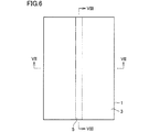
- the semiconductor substrate as the processing target 1 is configured in a substantially disc shape.
- An orientation flat 2 is provided on the outer periphery of a processing target (semiconductor substrate) 1.
- the processing target (semiconductor substrate) 1 is, for example, a silicon (Si) wafer or the like.
- a plurality of functional elements are provided on the surface 3 of the processing target (semiconductor substrate) 1. That is, the processing target (semiconductor substrate) 1 includes a substrate body and a plurality of functional elements arranged on the surface of the substrate body.
- the functional element is, for example, a semiconductor operation layer formed by crystal growth, a light receiving element such as a photodiode, a light emitting element such as a laser diode, or a circuit element formed as a circuit.
- a plurality of functional elements are provided in a matrix in a direction parallel to and perpendicular to the orientation flat 2 of the semiconductor substrate.
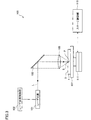
- the laser processing apparatus 100 includes a laser light source 101 that pulse-oscillates laser light (processing laser light) L and dichroics arranged so as to change the direction of the optical axis of the laser light L by 90 °.
- a mirror 103 and a focusing lens 105 for focusing the laser light L are provided.
- the laser processing apparatus 100 includes a support base 107 for supporting the processing target (semiconductor substrate) 1 to which the laser light L condensed by the condensing lens 105 is applied, and the support base 107 as X and Y.
- a stage 111 for moving in the Z-axis direction, a laser light source control unit 102 for controlling the laser light source 101 for adjusting the output and pulse width of the laser light L, and a stage control unit for controlling movement of the stage 111 And 115 are provided.
- the laser beam L emitted from the laser light source 101 is changed in the direction of its optical axis by 90 ° by the dichroic mirror 103, and the processing target object mounted on the support table 107 (semiconductor substrate ) Is collected by the condensing lens 105.
- the stage 111 is moved, and the object to be processed (semiconductor substrate) 1 is moved relative to the laser light L along the line to cut.
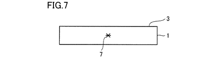
- a modified region to be a starting point of cutting is formed on the processing target (semiconductor substrate) 1.
- this reforming region will be described in detail.
- a planned cutting line 5 for cutting the processing target (semiconductor substrate) 1 is set in the plate-shaped processing target (semiconductor substrate) 1.
- the line to cut 5 is a virtual line extending linearly.
- the laser light L is scheduled to be cut in a state in which the focusing point P is aligned with the inside of the processing target (semiconductor substrate) 1. It is moved relatively along the line 5 (ie, in the direction of arrow A in FIG. 4).
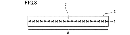
- the modified region 7 is formed along the planned cutting line 5 in the object (semiconductor substrate) 1 and is formed along the planned cutting line 5.
- the reforming region 7 becomes the cutting start region 8.
- the focusing point P is a portion where the laser light L is focused.
- the planned cutting line 5 is not limited to a straight line but may be a curved line, or may be a line drawn actually on the surface 3 of the processing target 1 without being limited to an imaginary line.
- the reforming region 7 may be formed continuously or may be formed intermittently.
- the modified region 7 may be formed at least inside the object 1 to be processed.
- a crack may be formed starting from the modified region 7, and the crack and the modified region 7 may be exposed to the outer surface (surface, back surface, or outer peripheral surface) of the processing target 1.
- the modified region 7 refers to a region in which the density, refractive index, mechanical strength and other physical properties are different from those in the surrounding area. For example, there are a melt processing region, a crack region, a dielectric breakdown region, a refractive index change region, and the like, and there are also regions in which these are mixed.
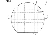
- the object to be processed (semiconductor substrate) 1 is fixed on the support table 107 of the laser processing apparatus 100. Then, with the surface 3 of the processing object (semiconductor substrate) 1 as the laser light incident surface, the condensing point P is aligned with the inside of the processing object (semiconductor substrate) 1 and the laser light L is irradiated. The focusing point P is scanned along the line to cut 5 which is set in a grid shape so as to pass between the adjacent functional elements. Further, on the planned cutting line 5, the condensing point P is scanned along the thickness direction of the processing target (semiconductor substrate) 1.
- the modified regions 7 are formed in a lattice on the object to be processed (semiconductor substrate) 1. Further, as shown in FIG. 10, in the inside of the processing target (semiconductor substrate) 1, the modified region 7 is formed from the front surface 3 side to the back surface 4 side of the processing target (semiconductor substrate) 1. That is, the modified region 7 is formed in the thickness direction of the processing target (semiconductor substrate) 1.
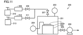
- the etching processing apparatus 200 includes a chamber 201, a stage (supporting material) 202, a pressure gauge 203, a thermometer 204, a valve 205, a vacuum pump 206, a valve 207, and a valve A flow controller 209, a first gas supply device 210, a valve 211, a flow controller 212, and a second gas supply device 213 are provided.
- the chamber 201 is configured to receive the processing target (semiconductor substrate) 1 in which the modified region 7 is formed.
- the object to be processed (semiconductor substrate) 1 is mounted on a stage 202 disposed in the chamber 201.
- the processing target (semiconductor substrate) 1 is fixed to the stage 202 by its own weight.
- the stage 202 may also include a suction device 202a.
- the processing target (semiconductor substrate) 1 is fixed to the stage 202 by the suction of the suction device 202a.
- the suction device 202a is, for example, an electrostatic chuck, a vacuum chuck or the like.
- the processing target (semiconductor substrate) 1 is fixed to the stage 202 by at least one of its own weight and adsorption.
- the stage 202 is configured to be adjustable in temperature. By heating the stage 202 while the processing target (semiconductor substrate) 1 is placed on the stage 202, the processing target (semiconductor substrate) 1 is heated so that the temperature becomes equal to that of the stage 202.
- a pressure gauge 203 for measuring the pressure in the chamber 201 is connected to the chamber 201.
- a thermometer 204 for measuring the temperature of the object 1 based on the temperature of the stage 202.
- the thermometer 204 is connected to the stage 202, and measures the temperature of the processing target (semiconductor substrate) 1 heated to the same temperature as the stage 202 by measuring the temperature of the stage 202.
- a vacuum pump 206 is connected to the chamber 201 by a pipe via a valve 205.
- the vacuum pump 206 is, for example, a turbo molecular pump, a mechanical booster pump, or the like.
- a first gas supply device 210 is connected to the chamber 201 by piping via a valve 207, a valve 208, and a flow rate controller 209.
- the first gas supply device 210 is configured to be able to supply an etching gas.
- a second gas supply device 213 is connected to the chamber 201 by piping via a valve 207, a valve 211, and a flow rate controller 212.
- the second gas supply device 213 is configured to be able to supply an etching gas.
- the etching gas supplied from the second gas supply device 213 may be the same etching gas as the etching gas supplied from the first gas supply device 210, or may be a different etching gas.
- the valve 205, the valve 207, the valve 208, and the valve 211 are, for example, electronic control valves.
- the flow controllers 209 and 212 are, for example, mass flow meters.
- the etching processing apparatus 200 includes the second gas supply apparatus 213 in addition to the first gas supply apparatus 210 in FIG. 11, only the first gas supply apparatus 210 may be provided. That is, the etching processing apparatus 200 may include only one gas supply apparatus. In addition, the etching processing apparatus 200 may include three or more gas supply apparatuses.
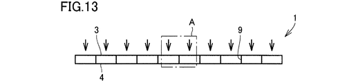
- dry etching processing is performed from the front surface 3 to the back surface 4 of the object to be processed (semiconductor substrate) 1.
- the dry etching process is, for example, an anisotropic dry etching process using a mixed gas of sulfur hexafluoride (SF 6 ), cyclopentafluoride (C 4 F 8 ) and oxygen (O 2 ). Thereby, the surface 3 of the processing target (semiconductor substrate) 1 is etched.
- a groove 9 is formed on the surface 3 of the object to be processed (semiconductor substrate) 1 along the line 5.
- the dry etching process may be performed in a state where, for example, a photoresist is formed on the functional element. The photoresist is removed at the end of the dry etch process.
- the dry etching process is performed from the front surface 3 to the back surface 4 of the processing object (semiconductor substrate) 1 in a state where the processing object (semiconductor substrate) 1 is fixed to the stage 202 by at least one of its own weight and adsorption.
- the groove 9 is formed to extend from the front surface 3 to the back surface 4 of the processing target (semiconductor substrate) 1.
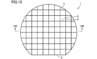
- FIGS. 14 to 16 correspond to the area A surrounded by the alternate long and short dash line in FIGS. 10 and 13, respectively.
- the object to be processed (semiconductor substrate) 1 is cut along the lines to be cut 5 shown in FIG. 4.
- Ru that is, as shown in FIG. 15, the dry etching process is performed on the processing target (semiconductor substrate) 1 from the front surface 3 to the back surface 4 of the processing target (semiconductor substrate) 1.
- the surface 3 of the processing target (semiconductor substrate) 1 is etched by the dry etching process.
- the groove 9 is formed in the middle of the modified region 7 from the front surface 3 to the back surface 4 of the processing target (semiconductor substrate) 1.
- the surface 3 of the object to be processed (semiconductor substrate) 1 is etched by further performing a dry etching process. Furthermore, the groove 9 is formed to extend from the front surface 3 to the back surface 4 of the object 1 to be processed. Thus, the object to be processed (semiconductor substrate) 1 is cut along the modified region 7. Moreover, in FIG. 12 and FIG. 13, the state where the distance between each chip which consists of the processed object (semiconductor substrate) 1 cut
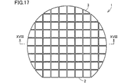
- the cut object (semiconductor substrate) 1 is divided into chips. That is, the distance between chips can be increased.
- FIGS. 17 and 18 show a state in which the distance between chips is maintained at a certain level or more. The distance between chips may be a distance suitable for the next step.
- the processing object (semiconductor substrate) 1 may be divided by being transferred to an expanding tape and the expanding tape being expanded (expanded).
- a halogen-based etching gas may be used for each of the first dry etching process and the second dry etching process.
- a halogen-based etching gas may be used for each of the first to nth dry etching processes.
- the halogen-based etching gases are chlorine trifluoride (ClF 3 ), nitrogen trifluoride (NF 3 ), sulfur hexafluoride (SF 6 ), fluorine (F 2 ), chlorine (Cl 2 ), hydrogen bromide ( It may contain at least one of HBr), carbon tetrafluoride (CF 4 ), cyclobutane octafluoride (C 4 F 8 ), methane trifluoride (CHF 3 ), and boron trichloride (BCl 3 ). That is, the halogen-based etching gas may be either a single gas or a mixed gas using these materials.
- the halogen-based etching gas may be, for example, a mixed gas of cyclobutane octafluoride (C 4 F 8 ) and oxygen (O 2 ).
- the object to be processed (semiconductor substrate) 1 is taken along the line to cut 5 It is cut off.
- the dry etching process is performed from the front surface 3 to the back surface 4 of the processing object (semiconductor substrate) 1 in a state where the processing object (semiconductor substrate) 1 is fixed to the stage 202 by at least one of its own weight and adsorption.
- the groove 9 is formed to extend from the front surface 3 to the back surface 4 of the object to be processed (semiconductor device) 1.
- the processing target (semiconductor substrate) 1 is cut along the line to cut 5.
- the expand tape in order to cut and divide the processing target (semiconductor substrate) 1. For this reason, it is possible to prevent the mechanical strength of the chip from being lowered due to surface roughening and cracking of the chip by the expand tape.
- the bonding area strength of the chips does not exceed the bonding area strength of the expand tape, it is possible to prevent the generation of a defect in the shape of the chip due to the expand tape.
- the reaction of the etching gas with the base material of the expand tape and the pressure-sensitive adhesive can prevent the expand tape from being deformed so as to expand and contract due to the chemical change and the heat change of the expand tape.
- the processing time is increased by the transfer step.
- the number of active species that react with the modified region 7 increases, so that the etching rate can be improved.
- the time required for etching can be significantly shortened, and the overall processing time can be shortened.
- a halogen-based etching gas can be used for the dry etching process.
- chlorine trifluoride (ClF 3 ), nitrogen trifluoride (NF 3 ), sulfur hexafluoride (SF 6 ), and fluorine respectively, as a halogen-based etching gas (F 2 ), chlorine (Cl 2 ), hydrogen bromide (HBr), carbon tetrafluoride (CF 4 ), cyclobutane octafluoride (C 4 F 8 ), methane trifluoride (CHF 3 ), boron trichloride At least one of (BCl 3 ) can be used.
- TEG Thermal Element Group
- TiN titanium nitride
- Mo molybdenum
- the processing target (semiconductor substrate) 1 includes a substrate body, a functional element (not shown), and the TEG 10.
- the material of the workpiece 1 may contain at least one of silicon (Si), tungsten (W), titanium (Ti), titanium nitride (TiN) and molybdenum (Mo).
- Si silicon
- Ti tungsten
- Ti titanium
- TiN titanium nitride
- Mo molybdenum
- plasma-less chlorine trifluoride (ClF 3 ) gas is used as a halogen-based etching gas
- the pressure of 10 Pa or more and 90 kPa (abs) or less, and each fluoride of the material Dry etching may be performed at a temperature higher than the boiling point and lower than 200 ° C. Again referring to FIG. 11, this pressure is the pressure in the chamber 201.
- This temperature is the temperature of the object 1 to be processed.
- the pressure is set to 10 Pa or more.
- the pressure is set to 10 Pa or more.
- the pressure is set to 10 Pa or more.
- the pressure can be set to 10 Pa using a mechanical booster pump instead of a turbo molecular pump, the pressure is set to 10 Pa or more.
- the pressure is made 90 kPa or less.
- etching can be performed over a pressure range of 10 Pa to 90 kPa (abs). For this reason, the pressure range is 10 Pa or more and 90 kPa (abs) or less.
- Chlorine trifluoride (ClF 3 ) gas can etch silicon (Si), tungsten (W), titanium (Ti), titanium nitride (TiN) and molybdenum (Mo).
- silicon (Si), tungsten (W), titanium (Ti), titanium nitride (TiN) and molybdenum (Mo) are used as the material of the object to be processed. Since the etching rate in each material can be secured by setting the boiling point or more of each fluoride of the material of the processing target 1, the temperature is made equal to or more than the boiling point of each fluoride of the material. Since the maximum temperature when dicing the device formed on the workpiece 1 is 200 ° C., the temperature is less than 200 ° C.
- the material of the object 1 is silicon (Si), tungsten (W), titanium (Ti), titanium nitride (TiN), and molybdenum At least one of Mo) may be included.
- plasma-less chlorine trifluoride (ClF 3 ) gas is used as a halogen-based etching gas, the pressure of 10 Pa or more and 90 kPa (abs) or less, and each fluoride of the material Dry etching may be performed at a temperature higher than the boiling point and lower than 200 ° C.
- the workpiece 1 containing at least one of silicon (Si), tungsten (W), titanium (Ti), titanium nitride (TiN) and molybdenum (Mo) can be etched.
- an insulating film may be formed on a line to be cut of the object to be processed.
- at least one of silicon dioxide (SiO 2 ), silicon oxynitride (SiON) and silicon nitride (SiN x) may be used as the material of the insulating film.
- SiNx has a width in the composition ratio (x) centering on Si 3 N 4 in which the ratio (composition) of the number of atoms constituting the SiN compound is present as the chemical formula.
- the value of x may be, for example, 1.0 or more and 1.5 or less.
- the object to be processed includes the substrate body, the functional element, and the insulating film.
- the material to be processed may include at least one of silicon dioxide (SiO 2 ), silicon oxynitride (SiON) and silicon nitride (SiN x).
- the first dry etching process and the second dry etching process may be performed in a state where anhydrous hydrogen fluoride (HF) is added to the halogen-based etching gas.
- the etching gas in which anhydrous hydrogen fluoride (HF) is added to the halogen-based etching gas can etch silicon dioxide (SiO 2 ), silicon oxynitride (SiON) and silicon nitride (SiN x). Therefore, the etching gas is in a state where anhydrous hydrogen fluoride (HF) is added to the halogen-based etching gas.
- the material of the object to be processed is at least one of silicon dioxide (SiO 2 ), silicon oxynitride (SiON) and silicon nitride (SiN x). May be included.
- dry etching may be performed in a state in which anhydrous hydrogen fluoride (HF) is added to the halogen-based etching gas.
- HF anhydrous hydrogen fluoride
- the workpiece 1 including at least one of silicon dioxide (SiO 2 ), silicon oxynitride (SiON), and silicon nitride (SiN x) can be etched.
- the pressure reduction process immediately before each dry etching process is performed.
- the volume density of the gas molecules may be changed in a range of 10 times or more and 10000 times or less.
- a TEG and an insulating film may be formed on a line to be cut of the object to be processed.
- tungsten (W), titanium (Ti), titanium nitride (TiN) and molybdenum (Mo) is used as the TEG material
- silicon dioxide (SiO 2 ) or nitrogen is used as the material of the insulating film.
- silicon oxide (SiON) and silicon nitride (SiNx) may be used.
- the material of the object to be processed is silicon (Si), tungsten (W), titanium (Ti), titanium nitride (TiN) and molybdenum (Mo), silicon dioxide (SiO 2 ), silicon oxynitride (SiON) and nitrided It may contain at least one of silicon (SiN x).
- oxygen (O 2 ) may be used, and dry etching may be performed at a pressure of 10 Pa to 0.8 kPa (abs) and a temperature of less than 200 ° C. This pressure is the pressure in the chamber. This temperature is the temperature of the object to be processed.
- silicon (Si), tungsten (W), titanium (Ti), titanium nitride (TiN) and molybdenum (Mo), silicon dioxide (SiO 2 ), silicon oxynitride (SiON) and nitride as materials of a processing object Silicon (SiN x) is used. Since the pressure at the maximum output of the remote plasma is 0.8 KPa, the pressure is 0.8 kPa (abs) or less.
- the material of the object to be processed is silicon (Si), tungsten (W), titanium (Ti), titanium nitride (TiN) and molybdenum (Mo) ), Silicon dioxide (SiO 2 ), silicon oxynitride (SiON) and / or silicon nitride (SiN x).
- oxygen (O 2 ) may be used, and dry etching may be performed at a pressure of 10 Pa to 0.8 kPa (abs) and a temperature of less than 200 ° C.
- Si silicon
- tungsten W
- Ti titanium
- TiN titanium nitride
- Mo molybdenum
- SiO 2 silicon dioxide
- SiON silicon oxynitride
- SiN x silicon nitride
- an aluminum film and TEG may be formed on a line to be cut of the object to be processed.
- aluminum (Al) is used as the material of the aluminum film
- at least one of tungsten (W), titanium (Ti), titanium nitride (TiN) and molybdenum (Mo) is used as the material of TEG.
- the material of the object to be processed may include at least one of aluminum (Al), silicon (Si), tungsten (W), titanium (Ti), titanium nitride (TiN) and molybdenum (Mo). .
- at least one of chlorine (Cl 2 ), hydrogen bromide (HBr), hydrogen chloride (HCl), and boron trichloride (BCl 3 ) of plasma is used as an etching gas.
- the dry etching process may be performed at a pressure of 10 Pa or more and 0.8 kPa (abs) or less and a temperature less than 200 ° C. This pressure is the pressure in the chamber. This temperature is the temperature of the object to be processed.
- the material of the object to be processed is aluminum (Al), silicon (Si), tungsten (W), titanium (Ti), titanium nitride (TiN) And / or molybdenum (Mo).
- at least one of chlorine (Cl 2 ), hydrogen bromide (HBr), hydrogen chloride (HCl) and boron trichloride (BCl 3 ) of plasma is used as an etching gas, and 10 Pa or more Dry etching may be performed at a pressure of 0.8 kPa (abs) or less and a temperature of less than 200 ° C.
- the pressure reduction process immediately before each dry etching process The pressure fluctuation may be changed to a range of 10% or more and 100% or less.
- the pressure of the substrate installation space is one of the discharge pressures while the pressure of the gas discharge space is maintained constant. It may be changed in the range of not less than 10 and not more than 1 / 10,000.
Landscapes
- Engineering & Computer Science (AREA)
- Physics & Mathematics (AREA)
- Optics & Photonics (AREA)
- Plasma & Fusion (AREA)
- Mechanical Engineering (AREA)
- Manufacturing & Machinery (AREA)
- Computer Hardware Design (AREA)
- Microelectronics & Electronic Packaging (AREA)
- Power Engineering (AREA)
- General Physics & Mathematics (AREA)
- Condensed Matter Physics & Semiconductors (AREA)
- High Energy & Nuclear Physics (AREA)
- Oil, Petroleum & Natural Gas (AREA)
- General Chemical & Material Sciences (AREA)
- Chemical Kinetics & Catalysis (AREA)
- Chemical & Material Sciences (AREA)
- Electromagnetism (AREA)
- Health & Medical Sciences (AREA)
- Toxicology (AREA)
- Drying Of Semiconductors (AREA)
- Dicing (AREA)
- Laser Beam Processing (AREA)
- Processing Of Stones Or Stones Resemblance Materials (AREA)
Priority Applications (5)
| Application Number | Priority Date | Filing Date | Title |
|---|---|---|---|
| KR1020207004267A KR20200029542A (ko) | 2017-07-20 | 2018-07-18 | 절단 가공 방법 |
| US16/632,298 US11482455B2 (en) | 2017-07-20 | 2018-07-18 | Cutting method of workpiece by forming reformed region and dry etching process |
| DE112018003720.7T DE112018003720B4 (de) | 2017-07-20 | 2018-07-18 | Schneideverfahren |
| CN201880048615.8A CN110998797B (zh) | 2017-07-20 | 2018-07-18 | 切割加工方法 |
| SG11202000317TA SG11202000317TA (en) | 2017-07-20 | 2018-07-18 | Cutting method |
Applications Claiming Priority (2)
| Application Number | Priority Date | Filing Date | Title |
|---|---|---|---|
| JP2017140872A JP6957252B2 (ja) | 2017-07-20 | 2017-07-20 | 切断加工方法 |
| JP2017-140872 | 2017-07-20 |
Publications (1)
| Publication Number | Publication Date |
|---|---|
| WO2019017368A1 true WO2019017368A1 (ja) | 2019-01-24 |
Family
ID=65015171
Family Applications (1)
| Application Number | Title | Priority Date | Filing Date |
|---|---|---|---|
| PCT/JP2018/026852 Ceased WO2019017368A1 (ja) | 2017-07-20 | 2018-07-18 | 切断加工方法 |
Country Status (8)
| Country | Link |
|---|---|
| US (1) | US11482455B2 (enExample) |
| JP (1) | JP6957252B2 (enExample) |
| KR (1) | KR20200029542A (enExample) |
| CN (1) | CN110998797B (enExample) |
| DE (1) | DE112018003720B4 (enExample) |
| SG (1) | SG11202000317TA (enExample) |
| TW (1) | TWI755553B (enExample) |
| WO (1) | WO2019017368A1 (enExample) |
Families Citing this family (2)
| Publication number | Priority date | Publication date | Assignee | Title |
|---|---|---|---|---|
| DE102019201438B4 (de) * | 2019-02-05 | 2024-05-02 | Disco Corporation | Verfahren zum Herstellen eines Substrats und System zum Herstellen eines Substrats |
| CN116374947B (zh) * | 2023-06-02 | 2023-08-25 | 中国工程物理研究院电子工程研究所 | 一种熔石英悬臂梁-质量块结构及其加工方法 |
Citations (3)
| Publication number | Priority date | Publication date | Assignee | Title |
|---|---|---|---|---|
| JP2014168790A (ja) * | 2013-03-01 | 2014-09-18 | Disco Abrasive Syst Ltd | ウエーハの加工方法 |
| JP2016035965A (ja) * | 2014-08-01 | 2016-03-17 | リンテック株式会社 | 板状部材の分割装置および板状部材の分割方法 |
| JP2017162856A (ja) * | 2016-03-07 | 2017-09-14 | 株式会社ディスコ | ウエーハの加工方法 |
Family Cites Families (18)
| Publication number | Priority date | Publication date | Assignee | Title |
|---|---|---|---|---|
| DE68928977T2 (de) * | 1988-02-09 | 1999-08-19 | Fujitsu Ltd. | Trockenätzen mit Wasserstoffbromid oder Brom |
| JPH0277579A (ja) * | 1988-06-06 | 1990-03-16 | Canon Inc | 堆積膜形成装置の洗浄方法 |
| US5536364A (en) * | 1993-06-04 | 1996-07-16 | Nippon Soken, Inc. | Process of plasma etching silicon |
| US6290864B1 (en) * | 1999-10-26 | 2001-09-18 | Reflectivity, Inc. | Fluoride gas etching of silicon with improved selectivity |
| JP2002151440A (ja) * | 2000-11-14 | 2002-05-24 | Sekisui Chem Co Ltd | ウェーハダイシング方法及びその装置 |
| JP2004359475A (ja) | 2003-06-02 | 2004-12-24 | Seiko Epson Corp | 光学素子の製造方法及び光学装置 |
| JP5041681B2 (ja) | 2004-06-29 | 2012-10-03 | 株式会社半導体エネルギー研究所 | 半導体装置の作製方法 |
| US7452786B2 (en) | 2004-06-29 | 2008-11-18 | Semiconductor Energy Laboratory Co., Ltd. | Method for manufacturing thin film integrated circuit, and element substrate |
| US20060032833A1 (en) * | 2004-08-10 | 2006-02-16 | Applied Materials, Inc. | Encapsulation of post-etch halogenic residue |
| KR101506355B1 (ko) | 2007-05-25 | 2015-03-26 | 하마마츠 포토닉스 가부시키가이샤 | 절단용 가공방법 |
| JP5264383B2 (ja) | 2008-09-17 | 2013-08-14 | 東京エレクトロン株式会社 | ドライエッチング方法 |
| US8847104B2 (en) * | 2008-12-05 | 2014-09-30 | Agency For Science Technology And Research | Wafer cutting method and a system thereof |
| CA2690697A1 (en) * | 2009-01-27 | 2010-07-27 | Air Products And Chemicals, Inc. | Selective etching and formation of xenon difluoride |
| WO2011021981A1 (en) * | 2009-08-17 | 2011-02-24 | Agency For Science, Technology And Research | Method of dicing a wafer |
| US20110061812A1 (en) | 2009-09-11 | 2011-03-17 | Applied Materials, Inc. | Apparatus and Methods for Cyclical Oxidation and Etching |
| US9129904B2 (en) | 2011-06-15 | 2015-09-08 | Applied Materials, Inc. | Wafer dicing using pulse train laser with multiple-pulse bursts and plasma etch |
| JP5939752B2 (ja) | 2011-09-01 | 2016-06-22 | 株式会社ディスコ | ウェーハの分割方法 |
| JP2016207737A (ja) * | 2015-04-17 | 2016-12-08 | 株式会社ディスコ | 分割方法 |
-
2017
- 2017-07-20 JP JP2017140872A patent/JP6957252B2/ja active Active
-
2018
- 2018-07-18 DE DE112018003720.7T patent/DE112018003720B4/de active Active
- 2018-07-18 SG SG11202000317TA patent/SG11202000317TA/en unknown
- 2018-07-18 CN CN201880048615.8A patent/CN110998797B/zh active Active
- 2018-07-18 TW TW107124815A patent/TWI755553B/zh active
- 2018-07-18 KR KR1020207004267A patent/KR20200029542A/ko not_active Ceased
- 2018-07-18 WO PCT/JP2018/026852 patent/WO2019017368A1/ja not_active Ceased
- 2018-07-18 US US16/632,298 patent/US11482455B2/en active Active
Patent Citations (3)
| Publication number | Priority date | Publication date | Assignee | Title |
|---|---|---|---|---|
| JP2014168790A (ja) * | 2013-03-01 | 2014-09-18 | Disco Abrasive Syst Ltd | ウエーハの加工方法 |
| JP2016035965A (ja) * | 2014-08-01 | 2016-03-17 | リンテック株式会社 | 板状部材の分割装置および板状部材の分割方法 |
| JP2017162856A (ja) * | 2016-03-07 | 2017-09-14 | 株式会社ディスコ | ウエーハの加工方法 |
Also Published As
| Publication number | Publication date |
|---|---|
| KR20200029542A (ko) | 2020-03-18 |
| DE112018003720B4 (de) | 2025-03-20 |
| US11482455B2 (en) | 2022-10-25 |
| CN110998797B (zh) | 2024-03-08 |
| DE112018003720T5 (de) | 2020-04-16 |
| CN110998797A (zh) | 2020-04-10 |
| JP2019021835A (ja) | 2019-02-07 |
| SG11202000317TA (en) | 2020-02-27 |
| TW201921469A (zh) | 2019-06-01 |
| TWI755553B (zh) | 2022-02-21 |
| JP6957252B2 (ja) | 2021-11-02 |
| US20200365461A1 (en) | 2020-11-19 |
Similar Documents
| Publication | Publication Date | Title |
|---|---|---|
| JP5762491B2 (ja) | エッチング方法 | |
| TWI725049B (zh) | 製造隔膜總成之方法及用於euv微影之隔膜總成 | |
| JP2020515047A5 (enExample) | ||
| KR101953044B1 (ko) | 규소 화합물용 에칭 가스 조성물 및 에칭 방법 | |
| CN102243989A (zh) | 通过热处理从所蚀刻的衬底去除卤素残余物的集成方法 | |
| CN103328688A (zh) | 具有改进的选择性的二氧化硅蒸汽蚀刻 | |
| CN113677825B (zh) | 沟槽中薄膜沉积的方法 | |
| JP5179455B2 (ja) | プラズマエッチング方法 | |
| WO2019017368A1 (ja) | 切断加工方法 | |
| CN114093761A (zh) | 蚀刻方法及等离子体处理装置 | |
| TW202139283A (zh) | 用於蝕刻用於半導體應用的材料層的方法 | |
| TWI760531B (zh) | 切斷加工方法(一) | |
| TW202439436A (zh) | 矽與鍺蝕刻 | |
| WO2009127738A1 (en) | A method of dicing wafers to give high die strength | |
| Shen et al. | A new etch planarization technology to correct non-uniformity post chemical mechanical polishing | |
| CN115831774B (zh) | 一种晶圆处理方法 | |
| JP6130313B2 (ja) | プラズマエッチング方法 | |
| Kang et al. | Study on the Etching selectivity of oxide films in dry cleaning process with NF3 and H2O | |
| US11195713B2 (en) | Methods of forming a silicon-insulator layer and semiconductor device having the same | |
| TW202507841A (zh) | 氮化矽之無鹵蝕刻 | |
| WO2022176142A1 (ja) | エッチング方法およびエッチング装置 | |
| CN104882375A (zh) | 一种防缺陷的半导体器件蚀刻方法及半导体器件形成方法 |
Legal Events
| Date | Code | Title | Description |
|---|---|---|---|
| 121 | Ep: the epo has been informed by wipo that ep was designated in this application |
Ref document number: 18836118 Country of ref document: EP Kind code of ref document: A1 |
|
| ENP | Entry into the national phase |
Ref document number: 20207004267 Country of ref document: KR Kind code of ref document: A |
|
| 122 | Ep: pct application non-entry in european phase |
Ref document number: 18836118 Country of ref document: EP Kind code of ref document: A1 |
|
| WWG | Wipo information: grant in national office |
Ref document number: 112018003720 Country of ref document: DE |
|
| WWG | Wipo information: grant in national office |
Ref document number: 11202000317T Country of ref document: SG |
|
| WWP | Wipo information: published in national office |
Ref document number: 11202000317T Country of ref document: SG |