WO2019012977A1 - 回路装置、回路装置の製造方法、およびコネクタ - Google Patents
回路装置、回路装置の製造方法、およびコネクタ Download PDFInfo
- Publication number
- WO2019012977A1 WO2019012977A1 PCT/JP2018/024097 JP2018024097W WO2019012977A1 WO 2019012977 A1 WO2019012977 A1 WO 2019012977A1 JP 2018024097 W JP2018024097 W JP 2018024097W WO 2019012977 A1 WO2019012977 A1 WO 2019012977A1
- Authority
- WO
- WIPO (PCT)
- Prior art keywords
- connector
- housing body
- circuit board
- biting
- resin
- Prior art date
- Legal status (The legal status is an assumption and is not a legal conclusion. Google has not performed a legal analysis and makes no representation as to the accuracy of the status listed.)
- Ceased
Links
Images




Classifications
-
- H—ELECTRICITY
- H05—ELECTRIC TECHNIQUES NOT OTHERWISE PROVIDED FOR
- H05K—PRINTED CIRCUITS; CASINGS OR CONSTRUCTIONAL DETAILS OF ELECTRIC APPARATUS; MANUFACTURE OF ASSEMBLAGES OF ELECTRICAL COMPONENTS
- H05K5/00—Casings, cabinets or drawers for electric apparatus
- H05K5/0026—Casings, cabinets or drawers for electric apparatus provided with connectors and printed circuit boards [PCB], e.g. automotive electronic control units
- H05K5/0034—Casings, cabinets or drawers for electric apparatus provided with connectors and printed circuit boards [PCB], e.g. automotive electronic control units having an overmolded housing covering the PCB
-
- H—ELECTRICITY
- H01—ELECTRIC ELEMENTS
- H01R—ELECTRICALLY-CONDUCTIVE CONNECTIONS; STRUCTURAL ASSOCIATIONS OF A PLURALITY OF MUTUALLY-INSULATED ELECTRICAL CONNECTING ELEMENTS; COUPLING DEVICES; CURRENT COLLECTORS
- H01R13/00—Details of coupling devices of the kinds covered by groups H01R12/70 or H01R24/00 - H01R33/00
- H01R13/46—Bases; Cases
- H01R13/50—Bases; Cases formed as an integral body
-
- H—ELECTRICITY
- H05—ELECTRIC TECHNIQUES NOT OTHERWISE PROVIDED FOR
- H05K—PRINTED CIRCUITS; CASINGS OR CONSTRUCTIONAL DETAILS OF ELECTRIC APPARATUS; MANUFACTURE OF ASSEMBLAGES OF ELECTRICAL COMPONENTS
- H05K3/00—Apparatus or processes for manufacturing printed circuits
- H05K3/22—Secondary treatment of printed circuits
- H05K3/28—Applying non-metallic protective coatings
- H05K3/284—Applying non-metallic protective coatings for encapsulating mounted components
-
- H—ELECTRICITY
- H05—ELECTRIC TECHNIQUES NOT OTHERWISE PROVIDED FOR
- H05K—PRINTED CIRCUITS; CASINGS OR CONSTRUCTIONAL DETAILS OF ELECTRIC APPARATUS; MANUFACTURE OF ASSEMBLAGES OF ELECTRICAL COMPONENTS
- H05K5/00—Casings, cabinets or drawers for electric apparatus
- H05K5/0026—Casings, cabinets or drawers for electric apparatus provided with connectors and printed circuit boards [PCB], e.g. automotive electronic control units
- H05K5/0069—Casings, cabinets or drawers for electric apparatus provided with connectors and printed circuit boards [PCB], e.g. automotive electronic control units having connector relating features for connecting the connector pins with the PCB or for mounting the connector body with the housing
-
- H—ELECTRICITY
- H10—SEMICONDUCTOR DEVICES; ELECTRIC SOLID-STATE DEVICES NOT OTHERWISE PROVIDED FOR
- H10W—GENERIC PACKAGES, INTERCONNECTIONS, CONNECTORS OR OTHER CONSTRUCTIONAL DETAILS OF DEVICES COVERED BY CLASS H10
- H10W74/00—Encapsulations, e.g. protective coatings
-
- H—ELECTRICITY
- H10—SEMICONDUCTOR DEVICES; ELECTRIC SOLID-STATE DEVICES NOT OTHERWISE PROVIDED FOR
- H10W—GENERIC PACKAGES, INTERCONNECTIONS, CONNECTORS OR OTHER CONSTRUCTIONAL DETAILS OF DEVICES COVERED BY CLASS H10
- H10W74/00—Encapsulations, e.g. protective coatings
- H10W74/01—Manufacture or treatment
-
- H—ELECTRICITY
- H01—ELECTRIC ELEMENTS
- H01R—ELECTRICALLY-CONDUCTIVE CONNECTIONS; STRUCTURAL ASSOCIATIONS OF A PLURALITY OF MUTUALLY-INSULATED ELECTRICAL CONNECTING ELEMENTS; COUPLING DEVICES; CURRENT COLLECTORS
- H01R12/00—Structural associations of a plurality of mutually-insulated electrical connecting elements, specially adapted for printed circuits, e.g. printed circuit boards [PCB], flat or ribbon cables, or like generally planar structures, e.g. terminal strips, terminal blocks; Coupling devices specially adapted for printed circuits, flat or ribbon cables, or like generally planar structures; Terminals specially adapted for contact with, or insertion into, printed circuits, flat or ribbon cables, or like generally planar structures
- H01R12/70—Coupling devices
- H01R12/71—Coupling devices for rigid printing circuits or like structures
- H01R12/72—Coupling devices for rigid printing circuits or like structures coupling with the edge of the rigid printed circuits or like structures
- H01R12/722—Coupling devices for rigid printing circuits or like structures coupling with the edge of the rigid printed circuits or like structures coupling devices mounted on the edge of the printed circuits
- H01R12/724—Coupling devices for rigid printing circuits or like structures coupling with the edge of the rigid printed circuits or like structures coupling devices mounted on the edge of the printed circuits containing contact members forming a right angle
-
- H—ELECTRICITY
- H05—ELECTRIC TECHNIQUES NOT OTHERWISE PROVIDED FOR
- H05K—PRINTED CIRCUITS; CASINGS OR CONSTRUCTIONAL DETAILS OF ELECTRIC APPARATUS; MANUFACTURE OF ASSEMBLAGES OF ELECTRICAL COMPONENTS
- H05K1/00—Printed circuits
- H05K1/18—Printed circuits structurally associated with non-printed electric components
-
- H—ELECTRICITY
- H05—ELECTRIC TECHNIQUES NOT OTHERWISE PROVIDED FOR
- H05K—PRINTED CIRCUITS; CASINGS OR CONSTRUCTIONAL DETAILS OF ELECTRIC APPARATUS; MANUFACTURE OF ASSEMBLAGES OF ELECTRICAL COMPONENTS
- H05K2201/00—Indexing scheme relating to printed circuits covered by H05K1/00
- H05K2201/10—Details of components or other objects attached to or integrated in a printed circuit board
- H05K2201/10007—Types of components
- H05K2201/10189—Non-printed connector
-
- H—ELECTRICITY
- H05—ELECTRIC TECHNIQUES NOT OTHERWISE PROVIDED FOR
- H05K—PRINTED CIRCUITS; CASINGS OR CONSTRUCTIONAL DETAILS OF ELECTRIC APPARATUS; MANUFACTURE OF ASSEMBLAGES OF ELECTRICAL COMPONENTS
- H05K2201/00—Indexing scheme relating to printed circuits covered by H05K1/00
- H05K2201/10—Details of components or other objects attached to or integrated in a printed circuit board
- H05K2201/10227—Other objects, e.g. metallic pieces
- H05K2201/1031—Surface mounted metallic connector elements
-
- H—ELECTRICITY
- H05—ELECTRIC TECHNIQUES NOT OTHERWISE PROVIDED FOR
- H05K—PRINTED CIRCUITS; CASINGS OR CONSTRUCTIONAL DETAILS OF ELECTRIC APPARATUS; MANUFACTURE OF ASSEMBLAGES OF ELECTRICAL COMPONENTS
- H05K2203/00—Indexing scheme relating to apparatus or processes for manufacturing printed circuits covered by H05K3/00
- H05K2203/13—Moulding and encapsulation; Deposition techniques; Protective layers
- H05K2203/1305—Moulding and encapsulation
- H05K2203/1316—Moulded encapsulation of mounted components
-
- H—ELECTRICITY
- H05—ELECTRIC TECHNIQUES NOT OTHERWISE PROVIDED FOR
- H05K—PRINTED CIRCUITS; CASINGS OR CONSTRUCTIONAL DETAILS OF ELECTRIC APPARATUS; MANUFACTURE OF ASSEMBLAGES OF ELECTRICAL COMPONENTS
- H05K2203/00—Indexing scheme relating to apparatus or processes for manufacturing printed circuits covered by H05K3/00
- H05K2203/13—Moulding and encapsulation; Deposition techniques; Protective layers
- H05K2203/1305—Moulding and encapsulation
- H05K2203/1327—Moulding over PCB locally or completely
-
- H—ELECTRICITY
- H05—ELECTRIC TECHNIQUES NOT OTHERWISE PROVIDED FOR
- H05K—PRINTED CIRCUITS; CASINGS OR CONSTRUCTIONAL DETAILS OF ELECTRIC APPARATUS; MANUFACTURE OF ASSEMBLAGES OF ELECTRICAL COMPONENTS
- H05K3/00—Apparatus or processes for manufacturing printed circuits
- H05K3/30—Assembling printed circuits with electric components, e.g. with resistors
- H05K3/32—Assembling printed circuits with electric components, e.g. with resistors electrically connecting electric components or wires to printed circuits
- H05K3/34—Assembling printed circuits with electric components, e.g. with resistors electrically connecting electric components or wires to printed circuits by soldering
- H05K3/341—Surface mounted components
- H05K3/3421—Leaded components
- H05K3/3426—Leaded components characterised by the leads
-
- Y—GENERAL TAGGING OF NEW TECHNOLOGICAL DEVELOPMENTS; GENERAL TAGGING OF CROSS-SECTIONAL TECHNOLOGIES SPANNING OVER SEVERAL SECTIONS OF THE IPC; TECHNICAL SUBJECTS COVERED BY FORMER USPC CROSS-REFERENCE ART COLLECTIONS [XRACs] AND DIGESTS
- Y02—TECHNOLOGIES OR APPLICATIONS FOR MITIGATION OR ADAPTATION AGAINST CLIMATE CHANGE
- Y02P—CLIMATE CHANGE MITIGATION TECHNOLOGIES IN THE PRODUCTION OR PROCESSING OF GOODS
- Y02P70/00—Climate change mitigation technologies in the production process for final industrial or consumer products
- Y02P70/50—Manufacturing or production processes characterised by the final manufactured product
Definitions
- the technology disclosed by the present specification relates to a circuit device, a method of manufacturing the circuit device, and a connector.
- a structure As a waterproof structure of a circuit device including a circuit board and a connector fixed to the circuit board, a structure is known in which the entire circuit board and a portion of the connector fixed to the circuit board are covered with a mold resin. ing.
- the mold resin is molded by setting the circuit substrate and the connector in a mold and filling the mold with a molten resin (see Patent Document 1).
- the connector housing is strongly sandwiched between the upper and lower molding dies, so that the flow of resin is cut off between the connector housing and the molding dies, and the molten resin is restricted from leaking out of the dies.
- cutting off the flow of resin in this way is referred to as "breaking up of resin", and a portion that cuts off resin in a molding die is called a cutting up portion).
- the circuit device disclosed by the present specification is a circuit device including a circuit board, a connector fixed to the circuit board, and a resin portion covering the circuit board and the connector, wherein the connector is A housing main body, and a biting receiving portion protruding from the housing main body, the biting receiving portion extends from the protruding portion protruding outward from the housing main body and the protruding portion, and approaches the housing main body toward the tip And an inclined wall which is inclined as described above, and a part of the inclined wall is embedded in the resin portion.
- a process of setting a circuit board and a connector fixed to the circuit board in a molding die, and a molten resin inside the molding die A method of manufacturing a circuit device including a resin portion forming step of forming a resin portion covering the circuit board and the connector by pouring and curing, wherein the molding die presses the connector.
- a biting portion for cutting off the flow of resin to the outside of the molding die is provided between the connector and the connector, and the connector includes a housing body and a biting receiving portion projecting from the housing body, and the biting receiving portion A tree-like part, the part which protrudes outward from the housing body, and the flexible wall which extends from the part and which can be bent so as to approach the housing body; Wherein Kuikiri portion presses said flexible wall in the part forming process.
- the housing main body may include a cylindrical hood portion capable of receiving the mating connector therein, and the biting receiver may be continued from the hood portion.
- the hood portion is hollow inside, deformation is likely to occur when the portion to be subjected to the pressing force by the biting-off portion of the molding die becomes the hood portion for the convenience of the circuit device design. In such a case, it is possible to suppress the deformation of the hood by setting the bite receiving part to continue from the hood.
- the biting receiving portion may be disposed over the entire circumference of the housing body. According to such a configuration, deformation of the housing body can be reliably avoided.
- the circuit device According to the circuit device, the method of manufacturing the circuit device, and the connector disclosed by the present specification, it is possible to suppress the deformation of the housing body due to the pressing force from the molding die.
- the circuit device of the present embodiment is an ECU (Electrical Control Unit) 1 that is disposed in a tire house of a vehicle in an electric brake system and controls braking.
- the ECU 1 includes a circuit board 10, a connector 20 fixed to the circuit board 10, and a resin portion 50 made of a synthetic resin which is formed by molding and covers the circuit board 10 and the connector 20. Is equipped.
- the circuit board 10 is a member of a known configuration in which conductive paths (not shown) are formed by printed wiring technology on one surface or both surfaces of an insulating plate made of an insulating material and electronic parts (not shown) are mounted. It is.
- the connector 20 is assembled to the connector housing 21, two fixing brackets 31 for fixing the connector housing 21 to the circuit board 10, and the conductive path on the circuit board 10 assembled to the connector housing 21. And a plurality of terminal fittings 41 connected thereto.
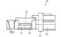
- the connector housing 21 is made of synthetic resin and, as shown in FIG. 3, includes a housing main body 22 and a bite receiving portion 27 continuous from the housing main body 22.
- the housing main body 22 includes a terminal holding wall 23, a hood portion 24 connected to the terminal holding wall 23, and a surrounding wall portion 25 connected to the terminal holding wall 23.
- the terminal holding wall 23 is a substantially plate-shaped portion for holding the terminal fitting 41, and has a plurality of press-fit holes 23H into which the terminal fitting 41 can be press-fitted.
- the hood portion 24 is a rectangular cylindrical portion extending from one surface of the terminal holding wall 23, and has an opening 24A on the opposite side to the terminal holding wall 23. The mating connector can be received in the internal space of the connector housing 21 surrounded by the terminal holding wall 23 and the hood portion 24.
- the surrounding wall portion 25 is a rectangular cylindrical portion extending from the terminal holding wall 23 in the direction opposite to the hood portion 24 as shown in FIG. 6, and a bottom wall 25A disposed along the circuit board 10; A top wall 25B parallel to the bottom wall 25A and two side walls 25C connecting the bottom wall 25A and the top wall 25B are formed. Each of the two side walls 25C has a mounting groove 26 as shown in FIG.
- the biting receiving portion 27 has a flange portion 28 (corresponding to a projecting portion) extending vertically outward from the hood portion 24 and a flexible wall extending perpendicularly from the extending end of the flange portion 28. And 29.
- the flexible wall 29 extends from the flange portion 28 in the direction approaching the terminal holding wall 23 (left direction in FIG. 6).
- the flexible wall 29 is disposed parallel to the hood portion 24 at an interval, and the end portion connected to the flange portion 28 is The base end portion 29A is formed, and the opposite end portion is bendable as a free end portion 29B in a direction approaching the hood portion 24.
- the bite receiving portion 27 is disposed over the entire circumference of the hood portion 24.
- Each of the two fixing brackets 31 is a member formed by pressing a metal plate material, and as shown in FIG. 3, a substantially rectangular main body portion 32 and a plate extending perpendicularly from one side of the main body portion 32 It has an attachment portion 33 in the form of a piece, and is L-shaped as a whole.
- a plurality of locking pieces are arranged on each of two side edges of the main body 32 (two sides perpendicular to one side to which the mounting part 33 is connected), and each mounting In the groove wall of the groove 26, an engagement receiving portion with which the plurality of locking pieces are engaged is disposed.
- one fixing bracket 31 is accommodated in the mounting groove 26 disposed in one side wall 25C, and the other fixing bracket 31 is accommodated in the mounting groove 26 disposed in the other side wall 25C. ing.
- Each fixing bracket 31 is held in the positioned state by the engagement of the locking piece with the engagement receiving portion.
- Each of the plurality of terminal fittings 41 is a member in which a long and thin plate material made of metal is bent, and as shown in FIG. 6, a tab portion 42 penetrating the terminal holding wall 23 and a substantially vertical from one end of the tab portion 42 And a board connecting portion 44 extending in the opposite direction from the tab portion 42 from the extending end of the middle portion.
- the tip of the tab portion 42 is disposed inside the hood portion 24.
- the intermediate portion 43 and the board connection portion 44 are disposed outside the connector housing 21.
- the board connection portion 44 is disposed along the circuit board 10 and is electrically connected to the conductive path by reflow soldering.
- the mounting portion 33 is disposed along the circuit board 10 and is fixed to the circuit board 10 by reflow soldering.
- the resin portion 50 covers the entire circuit board 10 and most of the connector 20 in a close contact state.
- the circuit board 10 is entirely embedded in the resin portion 50.
- a portion adjacent to the opening 24 A protrudes from the resin portion 50, and the remaining portion is embedded in the resin portion 50.
- the procedure for manufacturing the ECU 1 configured as described above is, for example, as follows.
- the terminal fitting 41 and the fixing fitting 31 are assembled to the connector housing 21.
- the connector 20 is fixed to the circuit board 10 by reflow soldering.
- solder is applied in advance to each portion on one surface of the circuit board 10 where soldering is planned.
- the connector 20 is placed on one surface of the circuit board 10.
- the hood portion 24 the portion where the biting receiving portion 27 is provided and the portion closer to the opening 24 A than this are projected from the edge of the circuit board 10, and the remaining portion is the circuit board 10. It is in the form of being arranged along one side.
- the board connection portion 44 of each terminal fitting 41 is placed on the solder, and the mounting portion 33 of each fixing fitting 31 is also placed on the solder.
- the circuit board 10 on which the connector 20 is mounted is run in a reflow furnace (not shown) to melt the solder. After that, when the solder is cooled and solidified, the board connection portions 44 of the respective terminal fittings 41 are fixed to the corresponding conductive paths and conduction is achieved, and the mounting portions 33 of the respective fixing brackets 31 are fixed to the circuit board 10 Be done.
- the connector housing 21 is fixed to the circuit board 10.
- the circuit board 10 on which the connector 20 is mounted is run in a reflow furnace (not shown) to melt the solder. After that, when the solder is cooled and solidified, the board connection portions 44 of the respective terminal fittings 41 are fixed to the corresponding conductive paths and conduction is achieved, and the mounting portions 33 of the respective fixing brackets 31 are fixed to the circuit board 10 Be done.
- the resin portion 50 is formed by molding.
- a molding die 60 for molding is formed of an upper die 61 and a lower die 62 which can be opened and closed in the vertical direction, and a resin portion is formed inside the molding die 60.
- a cavity 63 is formed in accordance with the shape of 50.
- the circuit board 10 to which the connector 20 is fixed is placed in the lower die 62, the upper die 61 is covered from above, and the molding die 60 is closed (setting step).
- the upper mold 61 is provided with an upper mold biting part 61A (biting part) and the lower mold 62 is provided with a lower mold biting part 62A (biting part), and the upper mold biting part 61A and the lower mold biting part 62A can be
- the connector housing 21 is firmly held between the upper mold 61 and the lower mold 62 while being in contact with the flexible wall 29 over the entire circumference.
- the flexible wall 29 is pressed by the upper die biting portion 61A and the lower die biting portion 62A and flexes toward the hood portion 24.
- the upper mold biting portion 61A and the lower mold biting portion 62A are strongly pressed against the flexible wall 29 by the force of the flexible wall 29 to be restored.
- the contact pressure between the upper die biting portion 61A and the lower die biting portion 62A is not directly received by the hood portion 24 but by the flexible wall 29, the deformation of the hood portion 24 is suppressed. be able to.
- molten resin is poured into the cavity 63 formed in the molding die 60 (resin part forming step).
- the upper die biting portion 61A and the lower die biting portion 62A are strongly pressed against the flexible wall 29, the upper die biting portion 61A, the lower die biting portion 62A, and the flexible wall 29 are obtained.
- the flow of the resin to the outside of the molding die 60 is cut off (breaking of the resin).
- the resin is cooled and cured. Thereby, the resin part 50 is formed.
- the mold 60 is opened in the vertical direction, and the completed ECU 1 is taken out of the mold.
- the molten resin is poured and cured in a state where the flexible wall 29 is bent by the upper die biting portion 61A and the lower die biting portion 62A, and therefore, in the completed ECU 1,
- the flexible wall 29 is inclined such that the free end 29B is closer to the hood 24 than the base end 29A, and constitutes an inclined wall.
- the free end portion 29B is embedded in the resin portion 50, and the remaining portion including the base end portion 29A (the portion to which the upper die biting portion 61A and the lower die biting portion 62A were in contact during molding) is the resin.
- the portion 50 is exposed to the outside.
- the ECU 1 of the present embodiment includes the circuit board 10, the connector 20 fixed to the circuit board 10, and the resin portion 50 covering the circuit board 10 and the connector 20.
- the connector 20 includes a housing body 22 and a bite receiving portion 27 projecting from the housing body 22.
- the bite receiving portion 27 includes a flange portion 28 projecting outward from the housing body 22 and a flexible wall 29 extending from the flange portion 28 and inclined so as to approach the housing body 22 as it goes to the tip, and the flexible wall 29 A part of is buried in the resin part 50.
- a molten resin is poured into the inside of the molding die 60, a setting step of setting the circuit substrate 10 and the connector 20 fixed to the circuit substrate 10 to the molding die 60. And a resin portion forming step of curing the resin.
- the molding die 60 includes an upper die biting portion 61A and a lower die biting portion 62A that cut the flow of resin to the outside of the molding die 60 with the connector 20 by pressing the connector 20.
- the connector 20 includes a housing body 22 and a biting receiving portion 27 projecting from the housing body 22.
- the biting receiving portion 27 extends from the flange portion 28 projecting outward from the housing body 22 and from the flange portion 28.
- a flexible wall 29 which can be bent to approach 22. Then, in the resin portion forming step, the upper die biting portion 61A and the lower die biting portion 62A press the flexible wall 29.
- the pressing force from the upper mold biting-off portion 61A and the lower mold biting-off portion 62A provided in the molding die 60 is received by the flexible wall 29. Therefore, deformation of the housing body 22 can be avoided.
- the housing body 22 is provided with a tubular hood portion 24 capable of accommodating the mating connector therein, and the bite receiving portion 27 is continued from the hood portion 24.
- the hood portion 24 has a hollow inside, and therefore, there is a possibility that the hood portion 24 may be deformed when the pressing force of the upper die biting portion 61A and the lower die biting portion 62A is directly received.
- the bite receiving portion 27 is configured to continue from the hood portion, deformation of the hood portion 24 can be suppressed.
- the bite receiving portion 27 is disposed over the entire circumference of the housing body 22, deformation of the housing body 22 can be reliably avoided.
- the flexible wall 29 extends in the direction (left direction in FIG. 2) approaching the terminal holding wall 23 from the flange portion 28, but the flexible wall extends from the flange portion 28 to the hood portion It may extend in the direction (right direction in FIG. 2) close to the opening 24A.
- the bite receiving portion 27 extends from the hood portion 24, but the bite receiving portion may be continued from a portion different from the hood portion 24 in the housing main body 22.
- biting receiving portion 27 is disposed over the entire circumference of the housing main body 22, even if the biting receiving portion is disposed only in a part of the housing main body 22, the deformation of the housing main body 22 A certain effect is exerted to suppress.
- ECU circuit device
- circuit board circuit board 20: connector 22: housing main body 24: hood portion 27: bite receiving portion 28: flange portion (projecting portion) 29: Flexible wall (tilted wall) 50: resin part 60: molding die 61A: upper mold eating out part (edging part) 62A: Lower mold eating out part
Landscapes
- Engineering & Computer Science (AREA)
- Microelectronics & Electronic Packaging (AREA)
- Manufacturing & Machinery (AREA)
- Manufacturing Of Electrical Connectors (AREA)
- Casings For Electric Apparatus (AREA)
- Structures Or Materials For Encapsulating Or Coating Semiconductor Devices Or Solid State Devices (AREA)
- Coupling Device And Connection With Printed Circuit (AREA)
- Non-Metallic Protective Coatings For Printed Circuits (AREA)
- Encapsulation Of And Coatings For Semiconductor Or Solid State Devices (AREA)
- Connector Housings Or Holding Contact Members (AREA)
Abstract
ECU1は、回路基板10と、回路基板10に固定されたコネクタ20と、回路基板10とコネクタ20とを覆う樹脂部50とを備えている。コネクタ20は、ハウジング本体22と、ハウジング本体22から突出する食い切り受部27とを備えている。食い切り受部27は、ハウジング本体22から外側に突出するフランジ部28と、フランジ部28から延び、先端に行くほどハウジング本体22に近づくように傾斜する可撓壁29とを備え、可撓壁29の一部が樹脂部50に埋設されている。
Description
本明細書によって開示される技術は、回路装置、回路装置の製造方法、およびコネクタに関する。
回路基板と、この回路基板に固着されたコネクタとを備える回路装置の防水構造として、回路基板の全体と、コネクタにおいて回路基板に固着されている部分とがモールド樹脂によって覆われた構造が知られている。モールド樹脂は、回路基板とコネクタとを成形金型にセットし、その金型内に溶融状態の樹脂を充填することにより、成形される(特許文献1参照)。
成形の際には、コネクタハウジングを上下の成形金型によって強く挟み込むことで、コネクタハウジングと成形金型との間で樹脂の流れを断ち切り、溶融樹脂が金型外に漏れ出すことを規制している(以下、このように樹脂の流れを断ち切ることを、「樹脂の食い切り」というものとし、成形金型において樹脂の食い切りを行う部分を食い切り部という)。このとき、樹脂を確実に食い切ろうとして成形金型をコネクタハウジングに強く押し付けると、コネクタハウジングに変形が生じてしまうおそれがある。
本明細書によって開示される回路装置は、回路基板と、前記回路基板に固定されたコネクタと、前記回路基板と前記コネクタとを覆う樹脂部とを備えた回路装置であって、前記コネクタが、ハウジング本体と、前記ハウジング本体から突出する食い切り受部とを備え、前記食い切り受部が、前記ハウジング本体から外側に突出する突出部と、前記突出部から延び、先端に行くほど前記ハウジング本体に近づくように傾斜する傾斜壁とを備え、前記傾斜壁の一部が前記樹脂部に埋設されている。
また、本明細書によって開示される回路装置の製造方法は、回路基板と、前記回路基板に固定されたコネクタとを成形金型にセットするセット工程と、前記成形金型の内部に溶融樹脂を流し込んで硬化させることにより、前記回路基板と前記コネクタとを覆う樹脂部を形成する樹脂部形成工程とを含む回路装置の製造方法であって、前記成形金型が、前記コネクタを押圧することで前記コネクタとの間で前記成形金型の外部への樹脂の流れを断ち切る食い切り部を備えており、前記コネクタが、ハウジング本体と、前記ハウジング本体から突出する食い切り受部とを備え、前記食い切り受部が、前記ハウジング本体から外側に突出する突出部と、前記突出部から延び、前記ハウジング本体に近づくように撓み可能な可撓壁とを備え、前記樹脂部形成工程において前記食い切り部が前記可撓壁を押圧する。
上記の構成によれば、樹脂部をモールド成形する工程において、成形金型に設けられた食い切り部からの押圧力を、可撓壁(傾斜壁)によって受けるようにできるから、ハウジング本体の変形を抑制できる。
上記の構成において、前記ハウジング本体が、相手側コネクタを内部に収容可能な筒状のフード部を備え、前記食い切り受部が前記フード部から連なっていても構わない。
フード部は、内部が空洞となっているため、回路装置の設計の都合上、成形金型の食い切り部による押圧力を受ける部分がフード部となってしまう場合、変形が生じる可能性が高い。このような場合に、食い切り受部がフード部から連なる構成とすることにより、フード部の変形を抑制できる。
上記の構成において、前記食い切り受部が前記ハウジング本体の全周にわたって配置されていても構わない。
このような構成によれば、ハウジング本体の変形を確実に回避できる。
このような構成によれば、ハウジング本体の変形を確実に回避できる。
本明細書によって開示される回路装置、回路装置の製造方法、およびコネクタによれば、成形金型からの押圧力によるハウジング本体の変形を抑制できる。
実施形態を、図1~図7を参照しつつ説明する。本実施形態の回路装置は、電動ブレーキシステムにおいて車両のタイヤハウス内に配され、ブレーキングを制御するためのECU(Electrical Cotrol Unit)1である。ECU1は、図2に示すように、回路基板10と、この回路基板10に固定されるコネクタ20と、モールド成形によって形成され、回路基板10とコネクタ20とを覆う合成樹脂製の樹脂部50とを備えている。
回路基板10は、絶縁材料からなる絶縁板の一面または両面に、プリント配線技術により導電路(図示せず)が形成されるとともに、電子部品(図示せず)が実装された周知の構成の部材である。
コネクタ20は、図3に示すように、コネクタハウジング21と、このコネクタハウジング21を回路基板10に固定するための2つの固定金具31と、コネクタハウジング21に組み付けられて回路基板10上の導電路と接続される複数の端子金具41とを備えている。
コネクタハウジング21は、合成樹脂製であって、図3に示すように、ハウジング本体22と、このハウジング本体22から連なる食い切り受部27とを備える。
ハウジング本体22は、図6に示すように、端子保持壁23と、この端子保持壁23から連なるフード部24と、同じく端子保持壁23から連なる囲み壁部25とを備える。
端子保持壁23は、図6に示すように、端子金具41を保持する略板状の部分であって、端子金具41を圧入可能な複数の圧入孔23Hを有している。フード部24は、図6に示すように、端子保持壁23の一面から延びる角筒状の部分であって、端子保持壁23とは反対側に開口部24Aを有している。端子保持壁23とフード部24とで囲まれるコネクタハウジング21の内部空間には、相手側コネクタを受け入れ可能となっている。
囲み壁部25は、図6に示すように、端子保持壁23からフード部24とは反対方向に延びる角筒状の部分であって、回路基板10に沿って配置される底壁25Aと、この底壁25Aと平行な天壁25Bと、底壁25Aと天壁25Bとを繋ぐ2つの側壁25Cとで構成されている。2つの側壁25Cのそれぞれは、図4に示すように、装着溝26を有している。
食い切り受部27は、図6に示すように、フード部24から外側に向かって垂直に延びるフランジ部28(突出部に該当)と、このフランジ部28の延出端から垂直に延びる可撓壁29とを備える。可撓壁29は、フランジ部28から端子保持壁23に近接する方向(図6の左方向)に延びている。可撓壁29は、樹脂部50がモールド成形により形成される前の状態では、フード部24に対して間隔を空けて、平行に配置されており、フランジ部28と接続している端部を基端部29Aとし、その反対側の端部を自由端部29Bとして、フード部24に対して近接する方向に撓み可能となっている。食い切り受部27は、フード部24の全周にわたって配置されている。
2つの固定金具31のそれぞれは、金属製の板材をプレス加工して形成された部材であり、図3に示すように、略矩形の本体部32と、本体部32の一辺から垂直に延びる板片状の取付部33とを備えて、全体としてL字状をなしている。本体部32の2つの側縁(取付部33が接続している1辺と垂直な2辺)のそれぞれには、詳細には図示しないが、複数の係止片が配置されており、各装着溝26の溝壁には、これら複数の係止片が係合する係合受部が配置されている。
図4に示すように、一方の固定金具31は、一方の側壁25Cに配された装着溝26に収容され、他方の固定金具31は、他方の側壁25Cに配された装着溝26に収容されている。各固定金具31は、係止片が係合受部に係合することで、位置決め状態で保持される。
複数の端子金具41のそれぞれは、金属製の細長い板材が屈曲された部材であって、図6に示すように、端子保持壁23を貫通するタブ部42と、タブ部42の一端から略垂直に延びる中間部43と、中間部の延出端からタブ部42と反対方向に延びる基板接続部44とにより構成されている。タブ部42の先端部は、フード部24の内部に配置されている。中間部43と基板接続部44とは、コネクタハウジング21の外部に配置されている。
コネクタ20が回路基板10に対して組み付けられた状態では、図2に示すように、フード部24において、食い切り受部27が設けられている部分、および、これよりも開口部24A側の部分が、回路基板10の端縁から外方(図2の右方)に突出され、残りの部分が、回路基板10の一面に沿って配置された形態となっている。基板接続部44は、回路基板10に沿って配置され、導電路に対しリフロー半田付けにより電気的に接続されている。また、詳細には図示しないが、取付部33は、回路基板10に沿うように配され、回路基板10に対しリフロー半田付けにより固着されている。
樹脂部50は、図2に示すように、回路基板10の全体と、コネクタ20の大部分とを密着状態で被覆している。回路基板10は、全体が樹脂部50の内部に埋設されている。コネクタ20は、開口部24Aに隣接する一部分が樹脂部50から突出しており、残りの部分が樹脂部50の内部に埋設されている。
上記のような構成のECU1を製造する手順は、例えば以下のようである。
まず、コネクタハウジング21に端子金具41と固定金具31とを組み付ける。
次に、リフローはんだ付けにより、コネクタ20を回路基板10に固定する。まず、回路基板10の一面において半田付けが予定されている各部位に予め半田を塗布する。続いて、コネクタ20を、回路基板10の一面に載置する。このとき、フード部24において、食い切り受部27が設けられている部分、および、これよりも開口部24A側の部分が、回路基板10の端縁から突出され、残りの部分が、回路基板10の一面に沿って配置された形態とする。コネクタ20が回路基板10に載置された状態では、各端子金具41の基板接続部44が半田上に載せられ、各固定金具31の取付部33も同じく半田上に載せられる。次に、コネクタ20を載せた回路基板10を図示しないリフロー炉内に走行させ、半田を溶融させる。そののち半田が冷却固化されると、各端子金具41の基板接続部44が対応する導電路に固着されて導通がとられるとともに、各固定金具31の取付部33が回路基板10に対して固着される。これにより、コネクタハウジング21が回路基板10に対して固定される。
次に、リフローはんだ付けにより、コネクタ20を回路基板10に固定する。まず、回路基板10の一面において半田付けが予定されている各部位に予め半田を塗布する。続いて、コネクタ20を、回路基板10の一面に載置する。このとき、フード部24において、食い切り受部27が設けられている部分、および、これよりも開口部24A側の部分が、回路基板10の端縁から突出され、残りの部分が、回路基板10の一面に沿って配置された形態とする。コネクタ20が回路基板10に載置された状態では、各端子金具41の基板接続部44が半田上に載せられ、各固定金具31の取付部33も同じく半田上に載せられる。次に、コネクタ20を載せた回路基板10を図示しないリフロー炉内に走行させ、半田を溶融させる。そののち半田が冷却固化されると、各端子金具41の基板接続部44が対応する導電路に固着されて導通がとられるとともに、各固定金具31の取付部33が回路基板10に対して固着される。これにより、コネクタハウジング21が回路基板10に対して固定される。
次に、コネクタ20を載せた回路基板10を図示しないリフロー炉内に走行させ、半田を溶融させる。そののち半田が冷却固化されると、各端子金具41の基板接続部44が対応する導電路に固着されて導通がとられるとともに、各固定金具31の取付部33が回路基板10に対して固着される。
次に、モールド成形により樹脂部50を形成させる。モールド成形を行うための成形金型60は、図7に示すように、上下方向に開閉可能な上型61と下型62とで構成されており、成形金型60の内部には、樹脂部50の形状に応じてキャビティ63が形成されている。
コネクタ20が固定された回路基板10を、下型62内に設置し、上型61を上方から被せて成形金型60を型閉じする(セット工程)。上型61は上型食い切り部61A(食い切り部)を、下型62は下型食い切り部62A(食い切り部)を、それぞれ備えており、上型食い切り部61Aと下型食い切り部62Aとが、可撓壁29に全周にわたって当接した状態で、コネクタハウジング21が上型61と下型62とにしっかりと挟み込まれる。可撓壁29は、上型食い切り部61Aと下型食い切り部62Aとによって押圧され、フード部24に向かって撓む。そして、可撓壁29が復元しようとする力によって、上型食い切り部61Aと下型食い切り部62Aとが可撓壁29に強く押し付けられた状態となる。このように上型食い切り部61Aと下型食い切り部62Aの接圧を、フード部24が直接受けるのではなく、可撓壁29によって受けるようになっているので、フード部24の変形を抑制することができる。
次に、成形金型60内に形成されたキャビティ63に溶融樹脂を流し込む(樹脂部形成工程)。このとき、上型食い切り部61Aと下型食い切り部62Aとが可撓壁29に強く押し付けられた状態となっていることによって、上型食い切り部61Aおよび下型食い切り部62Aと可撓壁29との間で、成形金型60の外部への樹脂の流れが断ち切られる(樹脂の食い切り)。
そして、成形金型60内に樹脂が満たされたところで、樹脂を冷却硬化させる。これにより、樹脂部50が形成される。
そして、成形金型60内に樹脂が満たされたところで、樹脂を冷却硬化させる。これにより、樹脂部50が形成される。
樹脂が硬化したところで、成形金型60を上下方向に型開きし、完成したECU1を金型から取り出す。上記の樹脂部形成工程において、上型食い切り部61Aと下型食い切り部62Aとで可撓壁29が撓まされた状態で溶融樹脂が流し込まれ、硬化されるので、完成したECU1においては、可撓壁29が、基端部29Aよりも自由端部29Bの方がフード部24に近づくように傾いた状態となり、傾斜壁を構成している。そして、自由端部29Bが樹脂部50に埋設されており、基端部29Aを含む残りの部分(成形の際に上型食い切り部61Aおよび下型食い切り部62Aが当接していた部分)が樹脂部50から外部に露出されている。
以上のように本実施形態のECU1は、回路基板10と、回路基板10に固定されたコネクタ20と、回路基板10とコネクタ20とを覆う樹脂部50とを備えている。コネクタ20は、ハウジング本体22と、ハウジング本体22から突出する食い切り受部27とを備えている。食い切り受部27は、ハウジング本体22から外側に突出するフランジ部28と、フランジ部28から延び、先端に行くほどハウジング本体22に近づくように傾斜する可撓壁29とを備え、可撓壁29の一部が樹脂部50に埋設されている。
また、本実施形態のECU1の製造方法は、回路基板10と、回路基板10に固定されたコネクタ20とを成形金型60にセットするセット工程と、成形金型60の内部に溶融樹脂を流し込んで硬化させる樹脂部形成工程とを含む。成形金型60は、コネクタ20を押圧することでコネクタ20との間で成形金型60の外部への樹脂の流れを断ち切る上型食い切り部61Aと下型食い切り部62Aとを備えている。コネクタ20は、ハウジング本体22と、ハウジング本体22から突出する食い切り受部27とを備え、食い切り受部27が、ハウジング本体22から外側に突出するフランジ部28と、フランジ部28から延び、ハウジング本体22に近づくように撓み可能な可撓壁29とを備えている。そして、樹脂部形成工程において、上型食い切り部61Aと下型食い切り部62Aとが可撓壁29を押圧する。
上記の構成によれば、樹脂部50をモールド成形する工程において、成形金型60に設けられた上型食い切り部61Aと下型食い切り部62Aからの押圧力を、可撓壁29によって受けるようにできるから、ハウジング本体22の変形を回避できる。
また、ハウジング本体22が、相手側コネクタを内部に収容可能な筒状のフード部24を備え、食い切り受部27がフード部24から連なっている。
フード部24は、内部が空洞となっているため、上型食い切り部61Aと下型食い切り部62Aによる押圧力を直接に受けると変形してしまうおそれがある。本実施形態では、食い切り受部27がフード部から連なる構成となっているので、フード部24の変形を抑制できる。
さらに、食い切り受部27がハウジング本体22の全周にわたって配置されているから、ハウジング本体22の変形を確実に回避できる。
<他の実施形態>
本明細書によって開示される技術は上記記述及び図面によって説明した実施形態に限定されるものではなく、例えば次のような種々の態様も含まれる。
(1)上記実施形態では、可撓壁29が、フランジ部28から端子保持壁23に近接する方向(図2の左方向)に延びていたが、可撓壁が、フランジ部28からフード部24の開口部24Aに近接する方向(図2の右方向)に延びていても構わない。
本明細書によって開示される技術は上記記述及び図面によって説明した実施形態に限定されるものではなく、例えば次のような種々の態様も含まれる。
(1)上記実施形態では、可撓壁29が、フランジ部28から端子保持壁23に近接する方向(図2の左方向)に延びていたが、可撓壁が、フランジ部28からフード部24の開口部24Aに近接する方向(図2の右方向)に延びていても構わない。
(2)上記実施形態では、食い切り受部27がフード部24から延びていたが、食い切り受部は、ハウジング本体22においてフード部24とは異なる部分から連なっていても構わない。
(3)上記実施形態では、食い切り受部27がハウジング本体22の全周にわたって配置されていたが、食い切り受部がハウジング本体22の一部にのみ配置されていても、ハウジング本体22の変形を抑制する一定の効果が奏される。
1:ECU(回路装置)
10:回路基板
20:コネクタ
22:ハウジング本体
24:フード部
27:食い切り受部
28:フランジ部(突出部)
29:可撓壁(傾斜壁)
50:樹脂部
60:成形金型
61A:上型食い切り部(食い切り部)
62A:下型食い切り部(食い切り部)
10:回路基板
20:コネクタ
22:ハウジング本体
24:フード部
27:食い切り受部
28:フランジ部(突出部)
29:可撓壁(傾斜壁)
50:樹脂部
60:成形金型
61A:上型食い切り部(食い切り部)
62A:下型食い切り部(食い切り部)
Claims (5)
- 回路基板と、前記回路基板に固定されたコネクタと、前記回路基板と前記コネクタとを覆う樹脂部とを備えた回路装置であって、
前記コネクタが、ハウジング本体と、前記ハウジング本体から突出する食い切り受部とを備え、
前記食い切り受部が、前記ハウジング本体から外側に突出する突出部と、前記突出部から延び、先端に行くほど前記ハウジング本体に近づくように傾斜する傾斜壁とを備え、前記傾斜壁の一部が前記樹脂部に埋設されている、回路装置。 - 前記ハウジング本体が、相手側コネクタを内部に収容可能な筒状のフード部を備え、
前記食い切り受部が前記フード部から連なっている、請求項1に記載の回路装置。 - 前記食い切り受部が前記ハウジング本体の全周にわたって配置されている、請求項1または請求項2に記載の回路装置。
- 回路基板と、前記回路基板に固定されたコネクタとを成形金型にセットするセット工程と、
前記成形金型の内部に溶融樹脂を流し込んで硬化させることにより、前記回路基板と前記コネクタとを覆う樹脂部を形成する樹脂部形成工程とを含む回路装置の製造方法であって、
前記成形金型が、前記コネクタを押圧することで前記コネクタとの間で前記成形金型の外部への樹脂の流れを断ち切る食い切り部を備えており、
前記コネクタが、ハウジング本体と、前記ハウジング本体から突出する食い切り受部とを備え、
前記食い切り受部が、前記ハウジング本体から外側に突出する突出部と、前記突出部から延び、前記ハウジング本体に近づくように撓み可能な可撓壁とを備え、
前記樹脂部形成工程において前記食い切り部が前記可撓壁を押圧する、回路装置の製造方法。 - ハウジング本体と、前記ハウジング本体から突出する食い切り受部とを備え、
前記食い切り受部が、前記ハウジング本体から外側に突出する突出部と、前記突出部から延び、前記ハウジング本体に近づくように撓み可能な可撓壁とを備えるコネクタ。
Priority Applications (2)
| Application Number | Priority Date | Filing Date | Title |
|---|---|---|---|
| US16/630,138 US10973137B2 (en) | 2017-07-12 | 2018-06-26 | Circuit device, method for manufacturing circuit device and connector |
| CN201880043707.7A CN110800093B (zh) | 2017-07-12 | 2018-06-26 | 电路装置、电路装置的制造方法以及连接器 |
Applications Claiming Priority (2)
| Application Number | Priority Date | Filing Date | Title |
|---|---|---|---|
| JP2017-135952 | 2017-07-12 | ||
| JP2017135952A JP6798436B2 (ja) | 2017-07-12 | 2017-07-12 | 回路装置、回路装置の製造方法、およびコネクタ |
Publications (1)
| Publication Number | Publication Date |
|---|---|
| WO2019012977A1 true WO2019012977A1 (ja) | 2019-01-17 |
Family
ID=65001295
Family Applications (1)
| Application Number | Title | Priority Date | Filing Date |
|---|---|---|---|
| PCT/JP2018/024097 Ceased WO2019012977A1 (ja) | 2017-07-12 | 2018-06-26 | 回路装置、回路装置の製造方法、およびコネクタ |
Country Status (4)
| Country | Link |
|---|---|
| US (1) | US10973137B2 (ja) |
| JP (1) | JP6798436B2 (ja) |
| CN (1) | CN110800093B (ja) |
| WO (1) | WO2019012977A1 (ja) |
Cited By (3)
| Publication number | Priority date | Publication date | Assignee | Title |
|---|---|---|---|---|
| WO2022070580A1 (ja) * | 2020-10-01 | 2022-04-07 | 株式会社オートネットワーク技術研究所 | コネクタ |
| CN115996538A (zh) * | 2021-10-20 | 2023-04-21 | 纬湃汽车电子(长春)有限公司 | 蓝牙功能保护结构、印刷电路板组件及传感器 |
| WO2026042787A1 (ja) * | 2024-08-20 | 2026-02-26 | 株式会社デンソー | 電子装置 |
Families Citing this family (5)
| Publication number | Priority date | Publication date | Assignee | Title |
|---|---|---|---|---|
| JP6801569B2 (ja) * | 2017-04-28 | 2020-12-16 | 株式会社オートネットワーク技術研究所 | 基板用コネクタ |
| JP7319594B2 (ja) * | 2020-03-06 | 2023-08-02 | 株式会社オートネットワーク技術研究所 | コネクタ装置 |
| US11431675B2 (en) | 2020-08-17 | 2022-08-30 | Arris Enterprises Llc | Client device based solution for handling MAC randomization |
| JP7670561B2 (ja) * | 2021-06-28 | 2025-04-30 | 日本航空電子工業株式会社 | コネクタ |
| WO2024232040A1 (ja) * | 2023-05-10 | 2024-11-14 | 日立Astemo株式会社 | 電子制御装置及び同製造方法 |
Citations (3)
| Publication number | Priority date | Publication date | Assignee | Title |
|---|---|---|---|---|
| JPH1076528A (ja) * | 1996-09-03 | 1998-03-24 | Fujitsu Ten Ltd | 金型構造及びコネクタの構造 |
| JPH10223667A (ja) * | 1997-02-03 | 1998-08-21 | Fujitsu Ten Ltd | 樹脂モールド基板の保持構造 |
| JP2001237557A (ja) * | 2000-02-24 | 2001-08-31 | Keihin Corp | 電子回路基板の収容ケース |
Family Cites Families (14)
| Publication number | Priority date | Publication date | Assignee | Title |
|---|---|---|---|---|
| JP3420673B2 (ja) * | 1996-12-03 | 2003-06-30 | 株式会社日立製作所 | 半導体装置及びその製造方法 |
| JP2002134642A (ja) * | 2000-10-20 | 2002-05-10 | Keihin Corp | ワイヤボンディング端子構造 |
| JP4601509B2 (ja) * | 2005-07-22 | 2010-12-22 | 日立オートモティブシステムズ株式会社 | モールド形電子回路装置及びその製造方法 |
| JP4884288B2 (ja) * | 2007-04-27 | 2012-02-29 | 三洋電機株式会社 | コネクタ装置およびその製造方法並びにそれを用いた電池パック |
| JP5020056B2 (ja) * | 2007-12-27 | 2012-09-05 | 帝国通信工業株式会社 | 電子部品の回路基板への取付方法 |
| JP2009200416A (ja) * | 2008-02-25 | 2009-09-03 | Mitsubishi Electric Corp | 半導体装置および半導体装置の製造方法 |
| JP2010040992A (ja) | 2008-08-08 | 2010-02-18 | Hitachi Ltd | 電子制御装置の製造方法とそのトランスファーモールド装置および電子制御装置 |
| JP2013232312A (ja) * | 2012-04-27 | 2013-11-14 | Jst Mfg Co Ltd | カード部材及びカードエッジコネクタ並びにカード部材の製造方法 |
| JP2014093414A (ja) * | 2012-11-02 | 2014-05-19 | Hitachi Automotive Systems Ltd | 電子制御装置 |
| JP2014093451A (ja) * | 2012-11-05 | 2014-05-19 | Denso Corp | モールドパッケージの製造方法 |
| JP5969405B2 (ja) * | 2013-01-30 | 2016-08-17 | 日立オートモティブシステムズ株式会社 | 車載用電子モジュール |
| JP6253402B2 (ja) * | 2013-12-27 | 2017-12-27 | 日立オートモティブシステムズ株式会社 | 車載用電子モジュール |
| JP6319665B2 (ja) * | 2014-08-08 | 2018-05-09 | 株式会社オートネットワーク技術研究所 | カードエッジコネクタ |
| JP6016965B2 (ja) * | 2015-03-02 | 2016-10-26 | 三菱電機株式会社 | 電子機器ユニット及びその製造金型装置 |
-
2017
- 2017-07-12 JP JP2017135952A patent/JP6798436B2/ja active Active
-
2018
- 2018-06-26 WO PCT/JP2018/024097 patent/WO2019012977A1/ja not_active Ceased
- 2018-06-26 CN CN201880043707.7A patent/CN110800093B/zh active Active
- 2018-06-26 US US16/630,138 patent/US10973137B2/en active Active
Patent Citations (3)
| Publication number | Priority date | Publication date | Assignee | Title |
|---|---|---|---|---|
| JPH1076528A (ja) * | 1996-09-03 | 1998-03-24 | Fujitsu Ten Ltd | 金型構造及びコネクタの構造 |
| JPH10223667A (ja) * | 1997-02-03 | 1998-08-21 | Fujitsu Ten Ltd | 樹脂モールド基板の保持構造 |
| JP2001237557A (ja) * | 2000-02-24 | 2001-08-31 | Keihin Corp | 電子回路基板の収容ケース |
Cited By (3)
| Publication number | Priority date | Publication date | Assignee | Title |
|---|---|---|---|---|
| WO2022070580A1 (ja) * | 2020-10-01 | 2022-04-07 | 株式会社オートネットワーク技術研究所 | コネクタ |
| CN115996538A (zh) * | 2021-10-20 | 2023-04-21 | 纬湃汽车电子(长春)有限公司 | 蓝牙功能保护结构、印刷电路板组件及传感器 |
| WO2026042787A1 (ja) * | 2024-08-20 | 2026-02-26 | 株式会社デンソー | 電子装置 |
Also Published As
| Publication number | Publication date |
|---|---|
| US10973137B2 (en) | 2021-04-06 |
| US20200137904A1 (en) | 2020-04-30 |
| CN110800093B (zh) | 2023-08-08 |
| JP6798436B2 (ja) | 2020-12-09 |
| CN110800093A (zh) | 2020-02-14 |
| JP2019021667A (ja) | 2019-02-07 |
Similar Documents
| Publication | Publication Date | Title |
|---|---|---|
| WO2019012977A1 (ja) | 回路装置、回路装置の製造方法、およびコネクタ | |
| CN107453108B (zh) | 电连接器及其制造方法 | |
| JP5454636B2 (ja) | 電気接続箱 | |
| CN110770979B (zh) | 电路装置 | |
| JP6844455B2 (ja) | 回路装置 | |
| JP4595655B2 (ja) | 電子回路装置およびその製造方法 | |
| CN110036538B (zh) | 用于机动车的变速器控制机构和用于制造插头壳体的方法 | |
| JP2017157286A (ja) | 樹脂成形品とその製造方法 | |
| JP2013004939A (ja) | 車載用電子モジュールの樹脂モールド方法 | |
| JP5326940B2 (ja) | 回路構成体及び電気接続箱 | |
| CN101320700A (zh) | 制造具有树脂模制外壳的电子装置的方法及模制工具 | |
| JP2010272637A (ja) | 電子部品の取付構造とその取付方法 | |
| CN104517925B (zh) | 半导体器件引线框架 | |
| JPH10242344A (ja) | 電力用半導体装置 | |
| JP2003282172A (ja) | プリント基板用コネクタ | |
| JP5293156B2 (ja) | 電気接続箱 | |
| JP2015037103A (ja) | 半導体装置及び半導体装置の製造方法 | |
| JP2017526186A (ja) | 回路基板を接触させる装置 | |
| WO2019009150A1 (ja) | 回路装置 | |
| WO2014208006A1 (ja) | 電子装置およびその電子装置の製造方法 | |
| JP2010183696A (ja) | 回路構成体および電気接続箱 | |
| JP2006012599A (ja) | 端子構造 | |
| JP2020021832A (ja) | 電子制御装置及び同製造方法 | |
| JP2011040686A (ja) | 電子機器及びその製造方法 | |
| JP2005005338A (ja) | 配線導体を用いた配線板 |
Legal Events
| Date | Code | Title | Description |
|---|---|---|---|
| 121 | Ep: the epo has been informed by wipo that ep was designated in this application |
Ref document number: 18832030 Country of ref document: EP Kind code of ref document: A1 |
|
| NENP | Non-entry into the national phase |
Ref country code: DE |
|
| 122 | Ep: pct application non-entry in european phase |
Ref document number: 18832030 Country of ref document: EP Kind code of ref document: A1 |