WO2018230619A1 - アーク溶接方法およびソリッドワイヤ - Google Patents
アーク溶接方法およびソリッドワイヤ Download PDFInfo
- Publication number
- WO2018230619A1 WO2018230619A1 PCT/JP2018/022643 JP2018022643W WO2018230619A1 WO 2018230619 A1 WO2018230619 A1 WO 2018230619A1 JP 2018022643 W JP2018022643 W JP 2018022643W WO 2018230619 A1 WO2018230619 A1 WO 2018230619A1
- Authority
- WO
- WIPO (PCT)
- Prior art keywords
- less
- wire
- mass
- copper plating
- plating film
- Prior art date
Links
- 238000003466 welding Methods 0.000 title claims abstract description 68
- 239000007787 solid Substances 0.000 title claims abstract description 61
- 238000000034 method Methods 0.000 title claims abstract description 37
- 239000010949 copper Substances 0.000 claims abstract description 77
- 238000007747 plating Methods 0.000 claims abstract description 70
- 229910052802 copper Inorganic materials 0.000 claims abstract description 69
- RYGMFSIKBFXOCR-UHFFFAOYSA-N Copper Chemical compound [Cu] RYGMFSIKBFXOCR-UHFFFAOYSA-N 0.000 claims abstract description 65
- 239000013078 crystal Substances 0.000 claims abstract description 48
- 229910000831 Steel Inorganic materials 0.000 claims abstract description 36
- 239000010959 steel Substances 0.000 claims abstract description 36
- 229910052717 sulfur Inorganic materials 0.000 claims description 8
- 229910001209 Low-carbon steel Inorganic materials 0.000 claims description 7
- 229910052782 aluminium Inorganic materials 0.000 claims description 5
- 229910052750 molybdenum Inorganic materials 0.000 claims description 5
- 229910052719 titanium Inorganic materials 0.000 claims description 4
- 229910052726 zirconium Inorganic materials 0.000 claims description 4
- 238000005491 wire drawing Methods 0.000 description 11
- 239000007789 gas Substances 0.000 description 10
- 239000002184 metal Substances 0.000 description 9
- 229910052751 metal Inorganic materials 0.000 description 9
- 230000000694 effects Effects 0.000 description 7
- 238000001953 recrystallisation Methods 0.000 description 7
- 239000002893 slag Substances 0.000 description 7
- 239000012535 impurity Substances 0.000 description 6
- 238000004519 manufacturing process Methods 0.000 description 5
- 238000012545 processing Methods 0.000 description 5
- 239000000463 material Substances 0.000 description 4
- 238000005259 measurement Methods 0.000 description 4
- 230000004927 fusion Effects 0.000 description 3
- 239000000203 mixture Substances 0.000 description 3
- 229910052760 oxygen Inorganic materials 0.000 description 3
- 229910052698 phosphorus Inorganic materials 0.000 description 3
- 239000000843 powder Substances 0.000 description 3
- NINIDFKCEFEMDL-UHFFFAOYSA-N Sulfur Chemical compound [S] NINIDFKCEFEMDL-UHFFFAOYSA-N 0.000 description 2
- QVGXLLKOCUKJST-UHFFFAOYSA-N atomic oxygen Chemical compound [O] QVGXLLKOCUKJST-UHFFFAOYSA-N 0.000 description 2
- 229910052799 carbon Inorganic materials 0.000 description 2
- 229910002091 carbon monoxide Inorganic materials 0.000 description 2
- 229910052804 chromium Inorganic materials 0.000 description 2
- 230000000052 comparative effect Effects 0.000 description 2
- 238000011156 evaluation Methods 0.000 description 2
- 230000020169 heat generation Effects 0.000 description 2
- 229910052748 manganese Inorganic materials 0.000 description 2
- 238000012986 modification Methods 0.000 description 2
- 230000004048 modification Effects 0.000 description 2
- 229910052759 nickel Inorganic materials 0.000 description 2
- 239000001301 oxygen Substances 0.000 description 2
- 238000004544 sputter deposition Methods 0.000 description 2
- 239000011593 sulfur Substances 0.000 description 2
- OAICVXFJPJFONN-UHFFFAOYSA-N Phosphorus Chemical compound [P] OAICVXFJPJFONN-UHFFFAOYSA-N 0.000 description 1
- 238000004220 aggregation Methods 0.000 description 1
- 230000002776 aggregation Effects 0.000 description 1
- 238000000137 annealing Methods 0.000 description 1
- 238000005452 bending Methods 0.000 description 1
- 230000015572 biosynthetic process Effects 0.000 description 1
- 230000015271 coagulation Effects 0.000 description 1
- 238000005345 coagulation Methods 0.000 description 1
- 238000010622 cold drawing Methods 0.000 description 1
- 238000005097 cold rolling Methods 0.000 description 1
- 238000009749 continuous casting Methods 0.000 description 1
- 229910000365 copper sulfate Inorganic materials 0.000 description 1
- ARUVKPQLZAKDPS-UHFFFAOYSA-L copper(II) sulfate Chemical compound [Cu+2].[O-][S+2]([O-])([O-])[O-] ARUVKPQLZAKDPS-UHFFFAOYSA-L 0.000 description 1
- 230000006866 deterioration Effects 0.000 description 1
- PEVJCYPAFCUXEZ-UHFFFAOYSA-J dicopper;phosphonato phosphate Chemical compound [Cu+2].[Cu+2].[O-]P([O-])(=O)OP([O-])([O-])=O PEVJCYPAFCUXEZ-UHFFFAOYSA-J 0.000 description 1
- 238000010438 heat treatment Methods 0.000 description 1
- 239000011261 inert gas Substances 0.000 description 1
- 229910000765 intermetallic Inorganic materials 0.000 description 1
- 239000011574 phosphorus Substances 0.000 description 1
- 239000002516 radical scavenger Substances 0.000 description 1
- 238000007670 refining Methods 0.000 description 1
- 229920006395 saturated elastomer Polymers 0.000 description 1
- 238000007790 scraping Methods 0.000 description 1
- 239000002436 steel type Substances 0.000 description 1
- 239000000758 substrate Substances 0.000 description 1
Images
Classifications
-
- B—PERFORMING OPERATIONS; TRANSPORTING
- B23—MACHINE TOOLS; METAL-WORKING NOT OTHERWISE PROVIDED FOR
- B23K—SOLDERING OR UNSOLDERING; WELDING; CLADDING OR PLATING BY SOLDERING OR WELDING; CUTTING BY APPLYING HEAT LOCALLY, e.g. FLAME CUTTING; WORKING BY LASER BEAM
- B23K35/00—Rods, electrodes, materials, or media, for use in soldering, welding, or cutting
- B23K35/22—Rods, electrodes, materials, or media, for use in soldering, welding, or cutting characterised by the composition or nature of the material
- B23K35/24—Selection of soldering or welding materials proper
- B23K35/30—Selection of soldering or welding materials proper with the principal constituent melting at less than 1550 degrees C
- B23K35/3053—Fe as the principal constituent
-
- B—PERFORMING OPERATIONS; TRANSPORTING
- B23—MACHINE TOOLS; METAL-WORKING NOT OTHERWISE PROVIDED FOR
- B23K—SOLDERING OR UNSOLDERING; WELDING; CLADDING OR PLATING BY SOLDERING OR WELDING; CUTTING BY APPLYING HEAT LOCALLY, e.g. FLAME CUTTING; WORKING BY LASER BEAM
- B23K9/00—Arc welding or cutting
- B23K9/16—Arc welding or cutting making use of shielding gas
- B23K9/173—Arc welding or cutting making use of shielding gas and of a consumable electrode
-
- B—PERFORMING OPERATIONS; TRANSPORTING
- B23—MACHINE TOOLS; METAL-WORKING NOT OTHERWISE PROVIDED FOR
- B23K—SOLDERING OR UNSOLDERING; WELDING; CLADDING OR PLATING BY SOLDERING OR WELDING; CUTTING BY APPLYING HEAT LOCALLY, e.g. FLAME CUTTING; WORKING BY LASER BEAM
- B23K35/00—Rods, electrodes, materials, or media, for use in soldering, welding, or cutting
- B23K35/02—Rods, electrodes, materials, or media, for use in soldering, welding, or cutting characterised by mechanical features, e.g. shape
- B23K35/0255—Rods, electrodes, materials, or media, for use in soldering, welding, or cutting characterised by mechanical features, e.g. shape for use in welding
- B23K35/0261—Rods, electrodes, wires
-
- B—PERFORMING OPERATIONS; TRANSPORTING
- B23—MACHINE TOOLS; METAL-WORKING NOT OTHERWISE PROVIDED FOR
- B23K—SOLDERING OR UNSOLDERING; WELDING; CLADDING OR PLATING BY SOLDERING OR WELDING; CUTTING BY APPLYING HEAT LOCALLY, e.g. FLAME CUTTING; WORKING BY LASER BEAM
- B23K35/00—Rods, electrodes, materials, or media, for use in soldering, welding, or cutting
- B23K35/22—Rods, electrodes, materials, or media, for use in soldering, welding, or cutting characterised by the composition or nature of the material
- B23K35/24—Selection of soldering or welding materials proper
- B23K35/30—Selection of soldering or welding materials proper with the principal constituent melting at less than 1550 degrees C
- B23K35/3026—Mn as the principal constituent
-
- B—PERFORMING OPERATIONS; TRANSPORTING
- B23—MACHINE TOOLS; METAL-WORKING NOT OTHERWISE PROVIDED FOR
- B23K—SOLDERING OR UNSOLDERING; WELDING; CLADDING OR PLATING BY SOLDERING OR WELDING; CUTTING BY APPLYING HEAT LOCALLY, e.g. FLAME CUTTING; WORKING BY LASER BEAM
- B23K35/00—Rods, electrodes, materials, or media, for use in soldering, welding, or cutting
- B23K35/22—Rods, electrodes, materials, or media, for use in soldering, welding, or cutting characterised by the composition or nature of the material
- B23K35/24—Selection of soldering or welding materials proper
- B23K35/30—Selection of soldering or welding materials proper with the principal constituent melting at less than 1550 degrees C
- B23K35/3053—Fe as the principal constituent
- B23K35/3073—Fe as the principal constituent with Mn as next major constituent
-
- C—CHEMISTRY; METALLURGY
- C25—ELECTROLYTIC OR ELECTROPHORETIC PROCESSES; APPARATUS THEREFOR
- C25D—PROCESSES FOR THE ELECTROLYTIC OR ELECTROPHORETIC PRODUCTION OF COATINGS; ELECTROFORMING; APPARATUS THEREFOR
- C25D3/00—Electroplating: Baths therefor
- C25D3/02—Electroplating: Baths therefor from solutions
- C25D3/56—Electroplating: Baths therefor from solutions of alloys
- C25D3/58—Electroplating: Baths therefor from solutions of alloys containing more than 50% by weight of copper
-
- C—CHEMISTRY; METALLURGY
- C25—ELECTROLYTIC OR ELECTROPHORETIC PROCESSES; APPARATUS THEREFOR
- C25D—PROCESSES FOR THE ELECTROLYTIC OR ELECTROPHORETIC PRODUCTION OF COATINGS; ELECTROFORMING; APPARATUS THEREFOR
- C25D5/00—Electroplating characterised by the process; Pretreatment or after-treatment of workpieces
- C25D5/48—After-treatment of electroplated surfaces
- C25D5/50—After-treatment of electroplated surfaces by heat-treatment
-
- C—CHEMISTRY; METALLURGY
- C25—ELECTROLYTIC OR ELECTROPHORETIC PROCESSES; APPARATUS THEREFOR
- C25D—PROCESSES FOR THE ELECTROLYTIC OR ELECTROPHORETIC PRODUCTION OF COATINGS; ELECTROFORMING; APPARATUS THEREFOR
- C25D5/00—Electroplating characterised by the process; Pretreatment or after-treatment of workpieces
- C25D5/60—Electroplating characterised by the structure or texture of the layers
- C25D5/615—Microstructure of the layers, e.g. mixed structure
- C25D5/617—Crystalline layers
-
- C—CHEMISTRY; METALLURGY
- C25—ELECTROLYTIC OR ELECTROPHORETIC PROCESSES; APPARATUS THEREFOR
- C25D—PROCESSES FOR THE ELECTROLYTIC OR ELECTROPHORETIC PRODUCTION OF COATINGS; ELECTROFORMING; APPARATUS THEREFOR
- C25D7/00—Electroplating characterised by the article coated
- C25D7/06—Wires; Strips; Foils
- C25D7/0607—Wires
-
- B—PERFORMING OPERATIONS; TRANSPORTING
- B23—MACHINE TOOLS; METAL-WORKING NOT OTHERWISE PROVIDED FOR
- B23K—SOLDERING OR UNSOLDERING; WELDING; CLADDING OR PLATING BY SOLDERING OR WELDING; CUTTING BY APPLYING HEAT LOCALLY, e.g. FLAME CUTTING; WORKING BY LASER BEAM
- B23K9/00—Arc welding or cutting
- B23K9/12—Automatic feeding or moving of electrodes or work for spot or seam welding or cutting
-
- C—CHEMISTRY; METALLURGY
- C25—ELECTROLYTIC OR ELECTROPHORETIC PROCESSES; APPARATUS THEREFOR
- C25D—PROCESSES FOR THE ELECTROLYTIC OR ELECTROPHORETIC PRODUCTION OF COATINGS; ELECTROFORMING; APPARATUS THEREFOR
- C25D5/00—Electroplating characterised by the process; Pretreatment or after-treatment of workpieces
- C25D5/34—Pretreatment of metallic surfaces to be electroplated
- C25D5/36—Pretreatment of metallic surfaces to be electroplated of iron or steel
Definitions
- the present embodiment relates to an arc welding method and a solid wire.
- Solid wire is widely used for gas shielded arc welding for thin plates of automobiles.
- wire feedability is excellent in short-term welding.
- the tip wears out due to fusion with the solid wire and the arc becomes unstable. Cheap.
- Patent Document 1 discloses a solid wire having a copper plating film with a thickness of 0.3 to 1.1 ⁇ m formed on the surface.
- the present invention has been made in view of the above-described problems, and an object of the present invention is to provide an arc welding method and a solid wire that have excellent feedability and high arc stability during arc welding.
- the present inventors have suppressed the wear of the copper plating film by reducing the crystal grain size of the copper plating film. I found out that I can do it. Furthermore, it has been found that the slidability of the solid wire can be improved, and, for example, in arc welding in which the feeding control is performed in the forward and backward direction of the solid wire, the feeding property can be improved and the arc during welding can be stabilized. It was. The present invention has been made based on this finding.
- one aspect of the arc welding method of the present invention includes a gas containing Ar, a steel core wire, and a copper plating film formed on the surface of the steel core wire, and an average crystal grain size of the copper plating film is 600 nm. Welding is performed using the following solid wire.
- the solid wire may be welded while being repeatedly fed and controlled in the forward / backward direction of the solid wire.
- the advancing / retreating direction means the forward direction and the reverse direction of wire feeding.
- the steel core wire may be made of mild steel.
- the solid wire is, by mass%, C: 0.02% to 0.15%, Si: 0.2% to 2.0%, Mn: 0 .2% to 3.0% and Cu: 0.05% to 0.5% may be contained.
- the solid wire is further mass%, S: 0.30% or less, Al: 0.1% or more and 1.0% or less, Mo: 0.00. It may include at least one of 1% to 3.0%, Ti: 0.01% to 0.3%, and Zr: 0.01% to 0.3%.
- the average crystal grain size of the copper plating film may be 50 nm or more and 500 nm or less.
- One aspect of the solid wire of the present invention is a solid wire comprising a steel core wire and a copper plating film formed on the surface of the steel core wire, wherein the average crystal grain size of the copper plating film is 600 nm or less. It is characterized by being.
- the steel core wire may be made of mild steel.
- One aspect of the solid wire of the present invention is, in mass%, C: 0.02% to 0.15%, Si: 0.2% to 2.0%, Mn: 0.2% to 3.0% % Or less, and Cu: 0.05% or more and 0.5% or less may be contained.
- One aspect of the solid wire of the present invention is further, in mass%, S: 0.30% or less, Al: 0.1% or more and 1.0% or less, Mo: 0.1% or more and 3.0% or less, At least one of Ti: 0.01% to 0.3% and Zr: 0.01% to 0.3% may be included.
- the average crystal grain size of the copper plating film may be 50 nm or more and 500 nm or less.
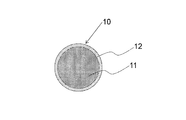
- FIG. 1 is a cross-sectional view of a solid wire according to an embodiment of the present invention.
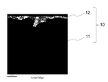
- FIG. 2 is an example of a measurement result of a solid wire section by EBSD.
- the arc welding method according to the embodiment of the present invention is a gas shielded arc welding method using the solid wire 10 shown in FIG.
- the solid wire 10 includes a steel core wire 11 and a copper plating film 12 formed on the surface of the steel core wire 11.
- the solid wire may be simply referred to as a wire.
- the steel core wire 11 is a wire made of steel having a circular cross section.
- the steel core wire 11 is mild steel, but is not limited thereto.
- mild steel means low carbon steel containing 0.01 mass% or more and 0.20 mass% or less of C.
- the copper plating film 12 is formed on the surface of the steel core wire 11 using a plating solution such as copper sulfate or copper pyrophosphate.
- a plating solution such as copper sulfate or copper pyrophosphate.
- the average crystal grain size of the copper plating film is 600 nm or less.
- the average crystal grain size of the copper plating film is 600 nm or less, wear of the copper plating film can be satisfactorily suppressed.
- the average crystal grain size of the copper plating film is preferably 500 nm or less. More preferably, it is 450 nm or less. Note that the average crystal grain size of the copper plating film is practically 50 nm or more.
- the average crystal grain size of the copper plating film in this embodiment is the area ratio of each crystal grain when the copper plating film having a cross section perpendicular to the longitudinal direction of the wire is measured using an EBSD (Electron Back-Scattered Diffraction) apparatus.
- This is a diameter that takes into account.
- the diameter d ′ in consideration of the area ratio is the ratio (c 1, c 2, c 3,%) Of any one crystal grain to the total area and the diameter (d 1, d2, d3, ...)
- d ' c1d1 + c2d2 + c3d3 + ...
- FIG. 2 is an example in which EBSD measurement is performed on the copper plating film 12 in a cross section orthogonal to the longitudinal direction of the solid wire 10 according to the embodiment of the present invention. More specifically, FIG. 2 is an IPF map, in which an orientation difference between crystal grains is 15 ° or more as a grain boundary. In this example, there are no coarse crystal grains having a grain size of 1 ⁇ m or more. The average crystal grain size d ′ of the copper plating film 12 shown in FIG. 2 is about 460 nm. In FIG. 2, the lower side is a steel core wire (base material) 11.
- the copper plating film 12 is formed by refining crystal grains by performing wire drawing processing and dynamic recrystallization after plating formation.
- the grain size of the copper plating film after plating is a mixed grain structure in which crystal grains of 1 ⁇ m or more and crystal grains with smaller grain sizes are mixed. As the size is reduced, the crystal grain size becomes more uniform. In the present embodiment, in the copper plating film 12 after dynamic recrystallization by wire drawing, crystal grains having a grain size exceeding 1 ⁇ m are not observed.
- the solid wire 10 is a wire having a circular cross section with a diameter of 0.6 mm to 1.8 mm, for example.
- the composition of the solid wire 10 is not particularly limited, but C: 0.02% by mass to 0.15% by mass, Si: 0.2% by mass to 2.0% by mass, Mn: 0.00%. It is preferable that 2 mass% or more and 3.0 mass% or less, Cu: 0.05 mass% or more and 0.5 mass% or less are included. Below, the reason for limitation of each component is demonstrated. In addition, content of these each element is content with respect to the wire total mass. Moreover, in this specification, the percentage (mass%) based on mass is synonymous with the percentage (weight%) based on weight.
- C in the welding wire or the weld metal affects the spatter generated during welding.
- sputtering there is no particular lower limit because there is no problem even if the content is small, but it is practical that it is 0.02% by mass or more.
- oxygen is contained in a large amount, it is combined with oxygen during welding and becomes CO gas, generating bubbles on the surface of the droplets. For this reason, it is preferable to prescribe
- C also affects the strength of the weld metal, and is preferably 0.04% by mass or more in order to ensure the strength.
- Si in the welding wire is a deoxidizing element and is an element that has an effect of ensuring the strength and toughness of the weld metal. If the addition amount is small, blowholes may be generated due to insufficient deoxidation, so it is preferable to contain 0.2% by mass or more. More preferably, it is 0.4 mass% or more. On the other hand, if Si is contained in a large amount, a large amount of slag is generated during welding, which may reduce the welding workability. For this reason, the Si content is preferably 2.0% by mass or less. More preferably, it is 1.5 mass% or less, More preferably, it is 1.0 mass% or less. In addition, when reducing generation
- Mn 0.2 mass% or more and 3.0 mass% or less
- Mn in the welding wire like Si, is necessary for exerting an effect as a deoxidizer or sulfur scavenger and ensuring the strength and toughness of the weld metal.
- Mn is contained in a large amount, a large amount of slag may be generated during welding, or the strength may increase excessively and the toughness of the weld metal may be significantly reduced.
- content of Mn is 3.0 mass% or less. More preferably, it is 2.0 mass% or less, More preferably, it is 1.3 mass% or less. In addition, when reducing generation
- Cu 0.05 mass% or more and 0.5 mass% or less
- Cu is mainly derived from the copper plating film and contained in the wire, but also includes Cu contained in the steel core wire.
- Cu is preferably 0.05% by mass or more.
- Cu is preferably 0.5% by mass or less, and more preferably 0.3% by mass or less.
- the balance of the solid wire is Fe and inevitable impurities. If necessary, at least one selected from S, P, Al, Mo, Ti and Zr may be further added within the following range.
- Other unavoidable impurities include, for example, N, O, Cr, Ni, and the like. In a solid wire, it is practical that N or O is 90 ppm or less. In addition, you may positively add Cr, Ni, etc.
- S (sulfur) and P (phosphorus) are both impurity elements, and it is preferable to make the content as small as possible. For this reason, a lower limit is not set, but it is practical that each is 0.001% by mass or more. . If these are present in large amounts exceeding 0.30% by mass, weld metal cracks may occur. Therefore, it is preferable to regulate both to 0.30 mass% or less (including 0%).
- Al 0.1% by mass or more and 1.0% by mass or less
- Al is an element that contributes to slag aggregation.
- the addition of Al is not essential, if the Al content is less than 0.1% by mass, it is difficult to obtain a coagulation effect of slag. Therefore, when adding Al, the content is 0.1% by mass or more. It is preferable to make it 0.2% by mass or more.
- the Al content exceeds 1.0% by mass, spattering may occur frequently. Therefore, when adding Al, the content is preferably 1.0% by mass or less, more preferably 0.7% by mass or less, and particularly preferably 0.4% by mass or less. preferable.
- Mo 0.1 mass% or more and 3.0 mass% or less
- Mo is an element that contributes to improvement in strength.
- addition of Mo is not essential, in order to exhibit such an effect well, when adding Mo, the content is preferably 0.1% by mass or more, and 0.3% by mass or more. It is more preferable.
- Mo exceeds 3.0% by mass the effect is saturated because it forms an intermetallic compound with Fe at a high temperature. Therefore, when adding Mo, the content is preferably 3.0% by mass or less, more preferably 2.0% by mass or less, and even more preferably 1.5% by mass or less. .
- Ti 0.01% by mass or more and 0.3% by mass or less
- Ti is a strong deoxidizing element and has the effect of improving the strength and toughness of the weld metal.
- it is preferable to contain 0.01% by mass or more. If it is contained in a large amount exceeding 0.3% by mass, a large amount of slag is generated during welding, and welding workability may be lowered. For this reason, it is preferable to regulate the Ti content in a range of 0.3 mass% or less.
- Zr 0.01 mass% or more and 0.3 mass% or less
- Zr has the effect of improving arc stability.
- the Zr content it is preferable to contain 0.01% by mass or more.
- the upper limit of the Zr content is preferably 0.3% by mass.
- molten steel having a predetermined component composition is melted using a converter, an electric furnace, or the like, and a steel material (a billet or the like) is produced from the obtained molten steel by continuous casting, an ingot forming method, or the like.
- a steel material a billet or the like
- the manufactured steel material is heated, it is subjected to hot working and further subjected to dry cold rolling (cold drawing) to obtain a steel strand having a diameter of about 3 to 8 mm, for example.
- the steel wire is annealed or pickled as necessary, and is subjected to copper plating and wire drawing to produce a solid wire 10 having a final wire diameter (eg, 0.6 to 1.8 mm).
- a well-known thing can be used as a plating bath at the time of copper plating.
- a wire drawing process for controlling the average crystal grain size of the copper plating film.
- a solid wire is drawn after copper plating.
- dynamic recrystallization and crystal grain growth occur in the copper plating film. That is, dynamic recrystallization occurs due to the introduction of strain due to processing, and the crystal grains become finer, and crystal grains grow due to heat generation due to processing, and the crystal grains become coarse.
- Japanese Patent Application Laid-Open No. 2012-143796 describes that the wire surface is exposed to a high temperature of 400 ° C. or higher during wire drawing. As described above, when the copper plating film is exposed to a high temperature during processing heat generation, the average crystal grain size grows to over 600 nm.
- the growth of crystal grains is suppressed while causing dynamic recrystallization.
- the frequency of occurrence of dynamic recrystallization can be controlled, for example, by adjusting the strain rate.
- the wire drawing rate for one pass is 20% or less, more preferably 15% or less, and even more preferably 10% or less.
- the strain rate is likely to be larger than that of a roller die, so that it is preferable to reduce the wire drawing rate.
- the wire may be cooled in advance to a temperature lower than normal temperature. As described above, the copper plating film 12 according to the embodiment of the present invention is obtained.
- arc welding method is performed using the solid wire 10 described above and a gas containing Ar.
- the shield gas used in the welding method according to the embodiment of the present invention only needs to contain Ar, and may consist only of Ar. Alternatively, in addition to Ar, CO 2 , O 2, or the like may be contained. For example, about 5 to 30% by volume of CO 2 to O 2 and the balance of Ar may be used.
- the shield gas can also contain N 2 , H 2, etc. as inevitable impurities.
- known welding conditions can be appropriately employed as the welding conditions.
- the material to be welded that is to be welded is not particularly limited, and can be applied to various steel plates.
- the average crystal grain size of the copper plating film 12 is 600 nm or less.
- the copper plating film is not easily damaged, the feedability is improved, and the arc can be stabilized.
- the copper plating film is energized inside the torch, it is energized while the copper plating film is well formed, so that chip fusion is stable, feedability is improved, and arc generation is also stable.
- the surface of the copper plating film is less likely to cause sliding wear and scraping with the contact object, and feedability and arc stability are improved.
- the advancing / retreating direction means the forward direction and the reverse direction of wire feeding.
- Comparative Example 1 is an example in which the wire used in Example 24 of the present invention was heat-treated in an inert gas atmosphere at a set temperature of a heating furnace of 200 ° C. for 10 minutes.
- the average crystal grain size was obtained using data measured in a cross section perpendicular to the longitudinal direction of the wire using an EBSD device (TSL OIM crystal orientation analyzer).
- the average crystal grain size is a diameter d ′ in consideration of the area ratio, and can be easily calculated by software attached to the apparatus.
- the numerical value of the average crystal grain size was rounded off to a multiple of 10 and rounded.
- the EBSD analysis range was 12.5 ⁇ m ⁇ 12.5 ⁇ m, and the measurement was performed under the conditions of step 0.035 ⁇ m.
- the evaluation criteria for the wire feedability are ⁇ as being particularly good when the amount of copper plating powder generated is particularly low in the inside of the feed path, ⁇ as indicating that the amount of copper plating powder generated is good, The case where there was much generation of copper plating powder was marked as x when it was not good.
- the good wire feedability means that the copper plating film is less likely to be worn or scraped when the wire is fed.
- the arc during the welding operation was visually evaluated, and the evaluation criteria were particularly good if the arc was consistently stable. ⁇ Some arcs were not stable The case where the product was good was marked as ⁇ , and the case where the arc was not consistently stable was marked as poor.
- the wire component (% by mass) represents the amount of each component (% by mass) per the total mass of the wire.
- the balance is Fe and inevitable impurities.
- “-” Means that the element is included as an inevitable impurity.
- Examples 1 to 26 of the present invention in which the average crystal grain size of the copper plating film of the wire was 600 nm or less were particularly good or good in feeding property and arc stability.
Landscapes
- Engineering & Computer Science (AREA)
- Chemical & Material Sciences (AREA)
- Mechanical Engineering (AREA)
- Metallurgy (AREA)
- Chemical Kinetics & Catalysis (AREA)
- Electrochemistry (AREA)
- Materials Engineering (AREA)
- Organic Chemistry (AREA)
- Crystallography & Structural Chemistry (AREA)
- Plasma & Fusion (AREA)
- Physics & Mathematics (AREA)
- Nonmetallic Welding Materials (AREA)
- Arc Welding In General (AREA)
Priority Applications (5)
| Application Number | Priority Date | Filing Date | Title |
|---|---|---|---|
| MX2019015302A MX2019015302A (es) | 2017-06-16 | 2018-06-13 | Metodo de soldadura con arco y alambre solido. |
| CN201880039116.2A CN110753597A (zh) | 2017-06-16 | 2018-06-13 | 电弧焊方法及实芯焊丝 |
| CA3067185A CA3067185C (en) | 2017-06-16 | 2018-06-13 | Arc welding method and solid wire |
| US16/622,666 US11407055B2 (en) | 2017-06-16 | 2018-06-13 | Arc welding method and solid wire |
| EP18816664.9A EP3626386A4 (en) | 2017-06-16 | 2018-06-13 | ARC WELDING PROCESS AND SOLID WIRE |
Applications Claiming Priority (2)
| Application Number | Priority Date | Filing Date | Title |
|---|---|---|---|
| JP2017118766A JP6788550B2 (ja) | 2017-06-16 | 2017-06-16 | アーク溶接方法およびソリッドワイヤ |
| JP2017-118766 | 2017-06-16 |
Publications (1)
| Publication Number | Publication Date |
|---|---|
| WO2018230619A1 true WO2018230619A1 (ja) | 2018-12-20 |
Family
ID=64658717
Family Applications (1)
| Application Number | Title | Priority Date | Filing Date |
|---|---|---|---|
| PCT/JP2018/022643 WO2018230619A1 (ja) | 2017-06-16 | 2018-06-13 | アーク溶接方法およびソリッドワイヤ |
Country Status (7)
Families Citing this family (7)
| Publication number | Priority date | Publication date | Assignee | Title |
|---|---|---|---|---|
| CN110358894A (zh) * | 2019-08-22 | 2019-10-22 | 中钢集团郑州金属制品研究院有限公司 | 一种弹簧钢丝晶粒细化热处理工艺 |
| WO2021157696A1 (ja) * | 2020-02-05 | 2021-08-12 | 日産自動車株式会社 | 溶射ワイヤー |
| JP7376411B2 (ja) * | 2020-03-31 | 2023-11-08 | 株式会社神戸製鋼所 | アーク溶接用ソリッドワイヤ |
| KR102461165B1 (ko) * | 2020-04-28 | 2022-11-03 | 주식회사 포스코 | 기가급 용접부를 얻을 수 있는 용접용 와이어, 이를 이용하여 제조된 용접구조물 및 그 용접방법 |
| EP4144478B1 (en) * | 2020-04-28 | 2025-09-10 | Posco | Welding wires for obtaining giga-grade welds, welded structures manufactured using same, and welding method thereof |
| JP7311473B2 (ja) * | 2020-09-02 | 2023-07-19 | 株式会社神戸製鋼所 | アーク溶接方法 |
| US20240009775A1 (en) | 2022-07-08 | 2024-01-11 | Daido Steel Co., Ltd. | Welding wire |
Citations (8)
| Publication number | Priority date | Publication date | Assignee | Title |
|---|---|---|---|---|
| JPS6043969B2 (ja) | 1982-06-09 | 1985-10-01 | 松下電器産業株式会社 | 調理機 |
| JPS613696A (ja) * | 1984-06-15 | 1986-01-09 | Daido Steel Co Ltd | 溶接ワイヤ |
| JP2002066785A (ja) * | 2000-08-28 | 2002-03-05 | Daido Steel Co Ltd | クロム系ステンレス鋼溶接ワイヤの製造方法 |
| JP2004314127A (ja) * | 2003-04-16 | 2004-11-11 | Nippon Steel Corp | 送給性に優れたアーク溶接用ソリッドワイヤ及びその製造方法 |
| JP2006326680A (ja) * | 2005-05-25 | 2006-12-07 | Kiswel Ltd | 溶接時におけるアーク安定性に優れた銅メッキマグ溶接用ソリッドワイヤ |
| JP2008194716A (ja) | 2007-02-13 | 2008-08-28 | Nippon Steel & Sumikin Welding Co Ltd | ガスシールドアーク溶接用銅めっきソリッドワイヤ |
| JP2012143796A (ja) | 2011-01-13 | 2012-08-02 | Nippon Steel & Sumikin Welding Co Ltd | 低温鋼溶接用Ni基合金フラックス入りワイヤ |
| JP2017118766A (ja) | 2015-12-25 | 2017-06-29 | 三菱自動車工業株式会社 | 車両のモータトルク推定装置 |
Family Cites Families (16)
| Publication number | Priority date | Publication date | Assignee | Title |
|---|---|---|---|---|
| JP3474393B2 (ja) * | 1997-03-31 | 2003-12-08 | 日鐵住金溶接工業株式会社 | 溶接用ワイヤの製造方法 |
| JP3071774B1 (ja) * | 1999-02-25 | 2000-07-31 | 高麗溶接棒ジャパン株式会社 | 送給性の優れた溶接用ソリッドワイヤ |
| US6608284B1 (en) * | 2000-05-17 | 2003-08-19 | Illinois Tool Works Inc. | Weld wire with enhanced slag removal |
| US20040140303A1 (en) * | 2002-01-31 | 2004-07-22 | Tokihiko Kataoka | Steel wire for carbon dioxide shielded arc welding and welding process using the same |
| US6784402B2 (en) * | 2002-03-27 | 2004-08-31 | Jfe Steel Corporation | Steel wire for MAG welding and MAG welding method using the same |
| JP2008049376A (ja) * | 2006-08-25 | 2008-03-06 | Daido Steel Co Ltd | 炭酸ガス溶接用ソリッドワイヤ |
| JP4839193B2 (ja) * | 2006-12-01 | 2011-12-21 | 株式会社神戸製鋼所 | ソリッドワイヤ |
| JP5066378B2 (ja) * | 2007-03-22 | 2012-11-07 | 日鐵住金溶接工業株式会社 | 溶融亜鉛系めっき鋼板のパルスmag溶接用銅めっきソリッドワイヤ |
| JP2009101376A (ja) * | 2007-10-22 | 2009-05-14 | Kobe Steel Ltd | 銅メッキあり溶接ワイヤ |
| CN101565842B (zh) * | 2009-05-15 | 2011-05-04 | 重庆理工大学 | 用滚动电沉积方法制造铜包铝导线的方法 |
| JP2012011461A (ja) * | 2010-05-31 | 2012-01-19 | Kobe Steel Ltd | 溶接用銅めっきソリッドワイヤ |
| CN101905392B (zh) * | 2010-08-26 | 2012-04-25 | 宜昌猴王焊丝有限公司 | 一种高韧性低合金实芯焊丝 |
| JP6043969B2 (ja) | 2012-03-07 | 2016-12-14 | パナソニックIpマネジメント株式会社 | 溶接方法 |
| KR101764519B1 (ko) * | 2013-02-15 | 2017-08-02 | 신닛테츠스미킨 카부시키카이샤 | 가스 실드 아크 용접용 솔리드 와이어, 가스 실드 아크 용접 금속, 용접 조인트, 용접 부재, 용접 방법 및 용접 조인트의 제조 방법 |
| CN106488823B (zh) * | 2014-09-08 | 2019-02-05 | 株式会社达谊恒 | 电弧焊接控制方法 |
| KR101579925B1 (ko) * | 2014-11-19 | 2015-12-29 | 현대종합금속 주식회사 | 마그 용접용 도금 솔리드 와이어 |
-
2017
- 2017-06-16 JP JP2017118766A patent/JP6788550B2/ja active Active
-
2018
- 2018-06-13 CA CA3067185A patent/CA3067185C/en active Active
- 2018-06-13 CN CN201880039116.2A patent/CN110753597A/zh active Pending
- 2018-06-13 US US16/622,666 patent/US11407055B2/en active Active
- 2018-06-13 MX MX2019015302A patent/MX2019015302A/es unknown
- 2018-06-13 WO PCT/JP2018/022643 patent/WO2018230619A1/ja unknown
- 2018-06-13 EP EP18816664.9A patent/EP3626386A4/en not_active Withdrawn
Patent Citations (8)
| Publication number | Priority date | Publication date | Assignee | Title |
|---|---|---|---|---|
| JPS6043969B2 (ja) | 1982-06-09 | 1985-10-01 | 松下電器産業株式会社 | 調理機 |
| JPS613696A (ja) * | 1984-06-15 | 1986-01-09 | Daido Steel Co Ltd | 溶接ワイヤ |
| JP2002066785A (ja) * | 2000-08-28 | 2002-03-05 | Daido Steel Co Ltd | クロム系ステンレス鋼溶接ワイヤの製造方法 |
| JP2004314127A (ja) * | 2003-04-16 | 2004-11-11 | Nippon Steel Corp | 送給性に優れたアーク溶接用ソリッドワイヤ及びその製造方法 |
| JP2006326680A (ja) * | 2005-05-25 | 2006-12-07 | Kiswel Ltd | 溶接時におけるアーク安定性に優れた銅メッキマグ溶接用ソリッドワイヤ |
| JP2008194716A (ja) | 2007-02-13 | 2008-08-28 | Nippon Steel & Sumikin Welding Co Ltd | ガスシールドアーク溶接用銅めっきソリッドワイヤ |
| JP2012143796A (ja) | 2011-01-13 | 2012-08-02 | Nippon Steel & Sumikin Welding Co Ltd | 低温鋼溶接用Ni基合金フラックス入りワイヤ |
| JP2017118766A (ja) | 2015-12-25 | 2017-06-29 | 三菱自動車工業株式会社 | 車両のモータトルク推定装置 |
Non-Patent Citations (1)
| Title |
|---|
| See also references of EP3626386A4 |
Also Published As
| Publication number | Publication date |
|---|---|
| US20200114453A1 (en) | 2020-04-16 |
| MX2019015302A (es) | 2020-02-17 |
| EP3626386A1 (en) | 2020-03-25 |
| US11407055B2 (en) | 2022-08-09 |
| JP2019000882A (ja) | 2019-01-10 |
| CN110753597A (zh) | 2020-02-04 |
| EP3626386A4 (en) | 2020-10-21 |
| CA3067185C (en) | 2022-03-22 |
| JP6788550B2 (ja) | 2020-11-25 |
| CA3067185A1 (en) | 2018-12-20 |
Similar Documents
| Publication | Publication Date | Title |
|---|---|---|
| WO2018230619A1 (ja) | アーク溶接方法およびソリッドワイヤ | |
| JP4839193B2 (ja) | ソリッドワイヤ | |
| US20040140303A1 (en) | Steel wire for carbon dioxide shielded arc welding and welding process using the same | |
| CN100509260C (zh) | 实芯焊丝 | |
| EP2610361B1 (en) | Flux-cored welding wire for carbon steel and process for arc welding | |
| JP5472244B2 (ja) | 厚鋼板の狭開先突合せ溶接方法 | |
| JP7711803B2 (ja) | 正極性mag溶接用ワイヤを用いた正極性mag溶接方法 | |
| JP6800770B2 (ja) | 薄鋼板のパルスmag溶接方法 | |
| JP2004195543A (ja) | ガスシールドアーク溶接用鋼ワイヤ | |
| JP6715622B2 (ja) | ソリッドワイヤ | |
| WO2017057194A1 (ja) | 高電流パルスアーク溶接方法及びフラックス入り溶接ワイヤ | |
| JP4228490B2 (ja) | パルスco2溶接方法 | |
| JP3753173B2 (ja) | ガスシールドアーク溶接用鋼ワイヤ | |
| JP2003225792A (ja) | 炭酸ガスシールドアーク溶接用ワイヤ | |
| JP3734030B2 (ja) | ガスシールドアーク溶接用鋼ワイヤ | |
| JP2005169414A (ja) | 炭酸ガスシールドアーク溶接用鋼ワイヤおよびそれを用いた溶接方法 | |
| JP2002283096A (ja) | ガスシールドアーク溶接用鋼ワイヤ | |
| JP5411796B2 (ja) | ガスシールドアーク溶接用ソリッドワイヤ | |
| JP3941756B2 (ja) | 炭酸ガスシールドアーク溶接用鋼ワイヤの鋼素線 | |
| JP2005219062A (ja) | Yagレーザアークハイブリッド溶接方法 | |
| JP5280060B2 (ja) | ガスシールドアーク溶接方法 | |
| JP2007118069A (ja) | ガスシールドアーク溶接方法 | |
| JP6928641B2 (ja) | ソリッドワイヤ | |
| JP2015167991A (ja) | 炭酸ガスシールドアーク溶接用ソリッドワイヤ | |
| JP3983155B2 (ja) | ガスシールドアーク溶接用鋼ワイヤ |
Legal Events
| Date | Code | Title | Description |
|---|---|---|---|
| 121 | Ep: the epo has been informed by wipo that ep was designated in this application |
Ref document number: 18816664 Country of ref document: EP Kind code of ref document: A1 |
|
| ENP | Entry into the national phase |
Ref document number: 3067185 Country of ref document: CA |
|
| NENP | Non-entry into the national phase |
Ref country code: DE |
|
| ENP | Entry into the national phase |
Ref document number: 2018816664 Country of ref document: EP Effective date: 20191219 |