WO2018159129A1 - 磁気抵抗効果素子 - Google Patents
磁気抵抗効果素子 Download PDFInfo
- Publication number
- WO2018159129A1 WO2018159129A1 PCT/JP2018/001187 JP2018001187W WO2018159129A1 WO 2018159129 A1 WO2018159129 A1 WO 2018159129A1 JP 2018001187 W JP2018001187 W JP 2018001187W WO 2018159129 A1 WO2018159129 A1 WO 2018159129A1
- Authority
- WO
- WIPO (PCT)
- Prior art keywords
- layer
- ferromagnetic layer
- effect element
- magnetoresistive effect
- nonmagnetic spacer
- Prior art date
Links
Images


Classifications
-
- H—ELECTRICITY
- H01—ELECTRIC ELEMENTS
- H01F—MAGNETS; INDUCTANCES; TRANSFORMERS; SELECTION OF MATERIALS FOR THEIR MAGNETIC PROPERTIES
- H01F10/00—Thin magnetic films, e.g. of one-domain structure
- H01F10/08—Thin magnetic films, e.g. of one-domain structure characterised by magnetic layers
- H01F10/10—Thin magnetic films, e.g. of one-domain structure characterised by magnetic layers characterised by the composition
- H01F10/18—Thin magnetic films, e.g. of one-domain structure characterised by magnetic layers characterised by the composition being compounds
- H01F10/193—Magnetic semiconductor compounds
- H01F10/1936—Half-metallic, e.g. epitaxial CrO2 or NiMnSb films
-
- H—ELECTRICITY
- H10—SEMICONDUCTOR DEVICES; ELECTRIC SOLID-STATE DEVICES NOT OTHERWISE PROVIDED FOR
- H10N—ELECTRIC SOLID-STATE DEVICES NOT OTHERWISE PROVIDED FOR
- H10N50/00—Galvanomagnetic devices
- H10N50/80—Constructional details
- H10N50/85—Magnetic active materials
-
- H—ELECTRICITY
- H01—ELECTRIC ELEMENTS
- H01F—MAGNETS; INDUCTANCES; TRANSFORMERS; SELECTION OF MATERIALS FOR THEIR MAGNETIC PROPERTIES
- H01F10/00—Thin magnetic films, e.g. of one-domain structure
- H01F10/32—Spin-exchange-coupled multilayers, e.g. nanostructured superlattices
- H01F10/324—Exchange coupling of magnetic film pairs via a very thin non-magnetic spacer, e.g. by exchange with conduction electrons of the spacer
- H01F10/3254—Exchange coupling of magnetic film pairs via a very thin non-magnetic spacer, e.g. by exchange with conduction electrons of the spacer the spacer being semiconducting or insulating, e.g. for spin tunnel junction [STJ]
-
- H—ELECTRICITY
- H01—ELECTRIC ELEMENTS
- H01F—MAGNETS; INDUCTANCES; TRANSFORMERS; SELECTION OF MATERIALS FOR THEIR MAGNETIC PROPERTIES
- H01F10/00—Thin magnetic films, e.g. of one-domain structure
- H01F10/32—Spin-exchange-coupled multilayers, e.g. nanostructured superlattices
- H01F10/324—Exchange coupling of magnetic film pairs via a very thin non-magnetic spacer, e.g. by exchange with conduction electrons of the spacer
- H01F10/3268—Exchange coupling of magnetic film pairs via a very thin non-magnetic spacer, e.g. by exchange with conduction electrons of the spacer the exchange coupling being asymmetric, e.g. by use of additional pinning, by using antiferromagnetic or ferromagnetic coupling interface, i.e. so-called spin-valve [SV] structure, e.g. NiFe/Cu/NiFe/FeMn
-
- H—ELECTRICITY
- H01—ELECTRIC ELEMENTS
- H01F—MAGNETS; INDUCTANCES; TRANSFORMERS; SELECTION OF MATERIALS FOR THEIR MAGNETIC PROPERTIES
- H01F10/00—Thin magnetic films, e.g. of one-domain structure
- H01F10/32—Spin-exchange-coupled multilayers, e.g. nanostructured superlattices
- H01F10/324—Exchange coupling of magnetic film pairs via a very thin non-magnetic spacer, e.g. by exchange with conduction electrons of the spacer
- H01F10/3286—Spin-exchange coupled multilayers having at least one layer with perpendicular magnetic anisotropy
-
- H—ELECTRICITY
- H10—SEMICONDUCTOR DEVICES; ELECTRIC SOLID-STATE DEVICES NOT OTHERWISE PROVIDED FOR
- H10N—ELECTRIC SOLID-STATE DEVICES NOT OTHERWISE PROVIDED FOR
- H10N50/00—Galvanomagnetic devices
- H10N50/10—Magnetoresistive devices
-
- H—ELECTRICITY
- H10—SEMICONDUCTOR DEVICES; ELECTRIC SOLID-STATE DEVICES NOT OTHERWISE PROVIDED FOR
- H10N—ELECTRIC SOLID-STATE DEVICES NOT OTHERWISE PROVIDED FOR
- H10N50/00—Galvanomagnetic devices
- H10N50/80—Constructional details
Definitions
- the present invention relates to a magnetoresistive element.
- the magnetoresistive effect element described in Patent Document 1 includes a first half metal ferromagnetic layer, a second half metal ferromagnetic layer, and a first half metal ferromagnetic layer and a second half metal ferromagnetic layer.
- At least one of the first half metal ferromagnetic layer and the second half metal ferromagnetic layer is made of a Heusler alloy, and the nonmagnetic metal layer is made of Ag.
- the present invention has been made in view of the above-described problems, and an object thereof is to provide a magnetoresistive effect element having a large magnetoresistive effect.
- a magnetoresistive element includes a first ferromagnetic layer as a magnetization fixed layer, a second ferromagnetic layer as a magnetization free layer, a first ferromagnetic layer, and a second ferromagnetic layer.
- the nonmagnetic spacer layer includes an Ag alloy represented by the general formula (1), whereby the nonmagnetic spacer layer, the first ferromagnetic layer, and / or Alternatively, the magnetoresistive element is such that the lattice mismatch with the second ferromagnetic layer is smaller than the lattice mismatch when the nonmagnetic spacer layer is made of Ag.
- X represents one element selected from the group consisting of Al, Cu, Ga, Ge, As, Y, La, Sm, Yb, and Pt, and ⁇ is 0 ⁇ ⁇ 1.
- the nonmagnetic spacer layer, the first ferromagnetic layer and / or the second ferromagnetic layer are compared with the nonmagnetic spacer layer compared to when the nonmagnetic spacer layer is made of Ag.
- An Ag alloy represented by the general formula (1) is included so that the lattice mismatch between and Therefore, according to this magnetoresistive effect element, since the crystallinity of the first ferromagnetic layer and / or the second ferromagnetic layer and the nonmagnetic spacer layer is improved, a large magnetoresistive effect can be exhibited. .
- the crystal structure of the Ag alloy represented by the general formula (1) may have a face-centered cubic lattice structure.
- the magnetoresistive element since the crystal structure of the Ag alloy can have a face-centered cubic lattice structure, the nonmagnetic spacer layer, the first ferromagnetic layer, and the second ferromagnetic layer have high crystal quality. Are stacked. Further, due to this high crystal quality, the magnetoresistive element according to the present invention can exhibit a large magnetoresistive effect.
- the crystal structure of the nonmagnetic spacer layer can stably take a face-centered cubic lattice structure.
- the nonmagnetic spacer layer, the first ferromagnetic layer, and the second ferromagnetic layer can be stacked with higher crystal quality, so that a greater magnetoresistance effect is exhibited.
- At least one of the first ferromagnetic layer and the second ferromagnetic layer may include a Heusler alloy represented by the general formula (2).
- L is at least one element of Mn and Fe
- M represents one or more elements selected from the group consisting of Si, Al, Ga, and Ge, and 0.7 ⁇ ⁇ 1 .6, and 0.65 ⁇ ⁇ 1.35.
- the Heusler alloys of the first ferromagnetic layer and the second ferromagnetic layer are: It has a lattice constant close to that of a stoichiometric composition. As a result, the lattice mismatch between the first ferromagnetic layer and / or the second ferromagnetic layer and the nonmagnetic spacer layer can be further reduced.
- X may be one element selected from the group consisting of Y, La, Sm, Yb, and Pt.
- the element contained in the first ferromagnetic layer and the second ferromagnetic layer and the element contained in the nonmagnetic spacer layer are mutually in the same group and period in the periodic table of elements. Does not belong to. Therefore, diffusion of elements contained in the first and second ferromagnetic layers and the nonmagnetic spacer layer is suppressed.
- the Heusler alloy contained in the first ferromagnetic layer and the second ferromagnetic layer can easily maintain the half-metal characteristics.
- a magnetoresistive effect element having a large magnetoresistive effect can be provided.
- Part (a) of FIG. 3 is a diagram showing the relationship between ⁇ and the normalized MR ratio
- part (b) of FIG. 3 is a diagram showing the relationship between ⁇ and the normalized MR ratio
- Part (c) of FIG. 3 is a diagram showing the relationship between ⁇ + ⁇ and the normalized MR ratio.
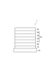
- FIG. 1 is a view showing a cross section of a magnetoresistive element according to an embodiment.
- the magnetoresistive effect element 1 includes a substrate 10, a crystal orientation layer 15, an underlayer 20, a magnetoresistive layer 30, and a cap layer 40 in this order.
- the magnetoresistive layer 30 includes a first ferromagnetic layer 31 as a magnetization free layer, a second ferromagnetic layer 32 as a magnetization fixed layer, and between the first ferromagnetic layer 31 and the second ferromagnetic layer 32.
- the second ferromagnetic layer 32 is provided on the nonmagnetic spacer layer 33, and the antiferromagnetic material layer 34 is provided on the second ferromagnetic layer 32.
- the magnetoresistive effect element 1 is manufactured by laminating the layers from the crystal orientation layer 15 to the cap layer 40 on the substrate 10 by a manufacturing method such as sputtering or vapor deposition.
- the magnetoresistive effect element 1 is a magnetoresistive effect element having a CPP (Current Perpendicular to Plane) structure in which a detection current flows along a stacking direction (a direction perpendicular to the film surface of each layer).
- the substrate 10 includes, for example, a metal oxide single crystal, a silicon single crystal, a silicon single crystal with a thermal oxide film, a sapphire single crystal, a ceramic, quartz, and glass.
- the material included in the substrate 10 is not particularly limited as long as it has an appropriate mechanical strength and is suitable for heat treatment and fine processing.
- the metal oxide single crystal include an MgO single crystal, and an epitaxial growth film can be easily formed according to a substrate including the MgO single crystal. This epitaxial growth film can exhibit a large magnetoresistance characteristic.
- the underlayer 20 can serve as an electrode for flowing a detection current, and includes, for example, at least one metal element of Ag, Au, Cu, Cr, V, Al, W, and Pt.
- the underlayer 20 may include an alloy of these metal elements or a laminate of materials made of two or more of these metal elements. Examples of metal element alloys include cubic AgZn alloys, AgMg alloys, and NiAl alloys.
- a crystal orientation layer 15 for controlling the crystal orientation of the upper layer may be provided between the base layer 20 and the substrate 10 as necessary.
- the crystal orientation layer 15 includes, for example, at least one of MgO, TiN, and NiTa alloy.
- the nonmagnetic spacer layer 33 includes an Ag alloy represented by the general formula (1).
- X is one element selected from the group consisting of Al, Cu, Ga, Ge, As, Y, La, Sm, Yb, and Pt, and ⁇ is 0 ⁇ ⁇ 1.
- the thickness of the nonmagnetic spacer layer 33 is, for example, 1 nm or more and 10 nm or less.
- the first ferromagnetic layer 31 functioning as a magnetization free layer is made of a soft magnetic material, and the magnetization direction is not substantially fixed. Therefore, when an external magnetic field is applied to the measurement object, the magnetization direction easily changes in that direction.
- the magnetization direction of the second ferromagnetic layer 32 functioning as a magnetization fixed layer is less likely to change than the magnetization direction of the first ferromagnetic layer 31 with respect to an external magnetic field.
- the magnetization direction of the second ferromagnetic layer 32 is substantially fixed with respect to the external magnetic field to be measured and does not substantially change with respect to the external magnetic field to be measured.
- the antiferromagnetic material layer 34 is provided on the surface of the second ferromagnetic layer 32 opposite to the nonmagnetic spacer layer 33 side.
- the antiferromagnetic layer 34 exchange-couples with the second ferromagnetic layer 32, and imparts unidirectional anisotropy to the second ferromagnetic layer 32, thereby causing the direction of magnetization of the second ferromagnetic layer 32. Is used for practical fixing.
- Examples of the material of the antiferromagnetic layer 34 include an FeMn alloy, a PtMn alloy, a PtCrMn alloy, a NiMn alloy, an IrMn alloy, NiO, and Fe 2 O 3 .
- the thickness of the first ferromagnetic layer 31 is 1 nm to 20 nm
- the thickness of the second ferromagnetic layer 32 is 1 nm to 20 nm
- the thickness of the antiferromagnetic material layer 34 is 5 nm to 15 nm.
- the coercive force of the second ferromagnetic layer 32 is changed by, for example, a technique such as changing the thickness of the layers.
- the antiferromagnetic layer 34 is not necessarily required. May not be provided.
- one of the first ferromagnetic layer 31 and the second ferromagnetic layer 32 may be a magnetization free layer and the other may be a magnetization fixed layer.
- the pinned layer and the second ferromagnetic layer 32 may be a magnetization free layer.
- the antiferromagnetic material layer 34 is provided on the surface of the second ferromagnetic layer 32 opposite to the nonmagnetic spacer layer 33 side.
- At least one of the first ferromagnetic layer 31 and the second ferromagnetic layer 32 can include a Heusler alloy represented by the general formula (2), and is preferably substantially made of the Heusler alloy.
- L is at least one element of Mn and Fe
- M is one or more elements selected from the group consisting of Si, Al, Ga, and Ge. Further, 0.7 ⁇ ⁇ 1.6 and 0.65 ⁇ ⁇ 1.35.
- the magnetoresistive element 1 is preferable because it can exhibit a large magnetoresistive effect. Further, since the conditions of 0.7 ⁇ ⁇ 1.6 and 0.65 ⁇ ⁇ 1.35 are satisfied, the Heusler alloy of the first ferromagnetic layer 31 and the second ferromagnetic layer 32 has a stoichiometric amount. It has a lattice constant close to that of a theoretical composition. Therefore, the effect described later that the lattice mismatch between the first ferromagnetic layer 31 and / or the second ferromagnetic layer 32 and the nonmagnetic spacer layer 33 is reduced is particularly remarkable. However, in the Heusler alloy, the conditions of 0.7 ⁇ ⁇ 1.6 and 0.65 ⁇ ⁇ 1.35 may not be satisfied.
- the crystal structure of the Heusler alloy can have a A2 structure, B2 structure or L2 1 structure.
- B2 structure Heusler alloy preferably has a high spin polarization than Heusler alloy A2 structure, Heusler alloy L2 1 structure is more preferable because it has a high spin polarization than Heusler alloy B2 structure.
- Table 1 is a table showing literature values of the spin polarizabilities P of some Heusler alloys, Fe and Co that satisfy the general formula (2). It is shown that the spin polarizability P of the Heusler alloy satisfying the general formula (2) is larger than the spin polarizability 46% of Fe and the spin polarizability 45% of Co.
- the first ferromagnetic layer 31 and the second ferromagnetic layer 32 can include Heusler alloys such as Co 2 CrIn and Co 2 CrSn, or ferromagnetic materials such as Fe 3 O 4 , CrO 2 , and CoFeB. Or it can consist essentially of the ferromagnetic material.
- the cap layer 40 is provided to protect the magnetoresistive layer 30.
- the cap layer 40 is made of, for example, one or more metal elements of Ru, Ag, Al, Cu, Au, Cr, Mo, Pt, W, Ta, Pd, and Ir, alloys of these metal elements, or of these metal elements A laminate of two or more types of materials may be included.
- heat treatment is performed as necessary. Further, a magnetic field application process is performed as necessary, and magnetic anisotropy such as uniaxial magnetic anisotropy is imparted to the first ferromagnetic layer 31 and / or the second ferromagnetic layer 32.
- the magnetic field application process may be performed together with the heat treatment.
- the nonmagnetic spacer layer 33 includes an Ag alloy represented by the general formula (1), whereby the nonmagnetic spacer layer 33 and the first ferromagnetic layer are included.
- the lattice mismatch between 31 and / or the second ferromagnetic layer 32 is smaller than the lattice mismatch when the nonmagnetic spacer layer 33 is assumed to be made of Ag.
- the lattice mismatch between the nonmagnetic spacer layer 33 made of Ag ⁇ Ga 1- ⁇ satisfying the general formula (1) and the first ferromagnetic layer 31 and / or the second ferromagnetic layer 32 is: This is smaller than the assumed lattice mismatch between the nonmagnetic spacer layer 33 assumed to be made of Ag and the first ferromagnetic layer 31 and / or the second ferromagnetic layer 32. Therefore, according to the magnetoresistive effect element 1 of the present embodiment, the crystallinity of the first ferromagnetic layer 31 and / or the second ferromagnetic layer 32 and the nonmagnetic spacer layer 33 is improved. A resistance effect can be exhibited.
- the crystal structure of the Ag alloy of the nonmagnetic spacer layer 33 may have a face-centered cubic lattice structure (fcc structure). Since the crystal structure of the Ag alloy can have an fcc structure, the nonmagnetic spacer layer 33, the first ferromagnetic layer 31, and the second ferromagnetic layer 32 are stacked with high crystal quality. Further, due to this high crystal quality, the magnetoresistive effect element according to the present embodiment can exhibit a large magnetoresistive effect. These effects are particularly remarkable when the crystal structures of the first ferromagnetic layer 31 and the second ferromagnetic layer 32 are also fcc structures.
- the magnetoresistive effect element 1 of the above-described embodiment 0.75 ⁇ ⁇ 1 may be satisfied for the Ag alloy included in the nonmagnetic spacer layer 33.
- the crystal structure of the nonmagnetic spacer layer 33 can be more stably taken to have an fcc structure, the nonmagnetic spacer layer 33, the first ferromagnetic layer 31 and the second ferromagnetic layer 32 are more It can be laminated with high crystal quality. This effect is particularly remarkable when the first ferromagnetic layer 31 and the second ferromagnetic layer 32 also have an fcc structure.
- the Ag alloy of the nonmagnetic spacer layer 33 may not satisfy 0.75 ⁇ ⁇ 1.
- the magnetoresistive effect element 1 of the present embodiment described above in the Ag alloy contained in the nonmagnetic spacer layer 33, ⁇ ⁇ 0.98 is preferable, and ⁇ ⁇ 0.96 is more preferable. Further, ⁇ ⁇ 0.90 is preferable, and ⁇ ⁇ 0.85 is more preferable.
- ⁇ has these values in the Ag alloy, the proportion of Ag contained in the nonmagnetic spacer layer 33 is reduced.
- the nonmagnetic spacer layer 33 in which the Ag ratio is reduced is different from the nonmagnetic spacer layer 33 made of Ag in that the nonmagnetic spacer layer 33, the first ferromagnetic layer 31 and / or the second ferromagnetic layer 32. In particular, the lattice mismatch can be reduced.
- X may be one element selected from the group consisting of Y, La, Sm, Yb, and Pt.
- the element included in the first ferromagnetic layer 31 and the second ferromagnetic layer 32 and the element included in the nonmagnetic spacer layer 33 do not belong to the same group and period in the periodic table of elements. . Therefore, diffusion of elements contained in the first ferromagnetic layer 31 and the second ferromagnetic layer 32 and the nonmagnetic spacer layer 33 is suppressed. This suppression of diffusion increases the magnetoresistive effect.
- X may be one element selected from the group consisting of La, Sm, Yb, and Pt.
- Tables 2 to 4 are tables for showing examples of lattice mismatch of the magnetoresistive effect element.
- Table 2 shows examples of materials (first to 28th examples) and Ag (29th example) that can constitute the nonmagnetic spacer layer 33 of this embodiment, and those materials have an fcc structure. It is a table
- Table 3 shows examples of materials (alloy A to alloy G) that can constitute the first ferromagnetic layer 31 and the second ferromagnetic layer 32 of the present embodiment, and literature values of lattice constants of these materials. It is a table.
- Table 4 is a table showing lattice mismatch rates of Alloy A to Alloy G shown in Table 3 for each of the first to 29th examples shown in Table 2.
- the lattice mismatch rate in Table 4 is expressed as a percentage, and is obtained by the following equation (3).
- Lattice mismatch rate (%) ((a ⁇ ⁇ 2 ⁇ b) / b) ⁇ 100 (%) (3)
- a represents the lattice constants of the first to 29th examples shown in Table 2
- b represents the lattice constants of Alloy A to Alloy G shown in Table 3.
- ⁇ 2 means the square root of 2.
- Equation (3) the lattice mismatch ratio between the [110] direction of each (001) plane of Examples 1 to 29 and the [100] direction of each (001) plane of Alloy A to Alloy G Is calculated.
- Table 4 also shows the evaluation results of the first to 28th examples.
- the examples showing the lattice mismatch rate smaller than the lattice mismatch rate in the 29th example with respect to six or more of the alloys A to G are “particularly good”. "A” meaning "”.
- the example showing the lattice mismatch rate smaller than the lattice mismatch rate in the 29th example is “good”. Evaluates to mean “B”.
- the evaluation is “A” or “B”.
- ⁇ is 0.75 ⁇ ⁇ 1 (first to fourth examples, seventh to eleventh examples, fourteenth to twenty-fourth examples, twenty-seventh example, and twenty-eighth example) In Example), it is evaluated as “A”. If the material of the example of evaluation B is used as the nonmagnetic spacer layer 33 of this embodiment, the crystallinity of the first ferromagnetic layer 31 and / or the second ferromagnetic layer 32 and the nonmagnetic spacer layer 33 is improved.
- Table 5 shows a nonmagnetic spacer layer Ag alloy, first ferromagnetic layer, and second ferromagnetic layer Heusler alloy in magnetoresistive elements according to Examples 1 to 25 and Comparative Example 1 prepared as described below.
- the magnetoresistance ratio (MR ratio) in the magnetoresistive effect element is estimated from the magnitude of the measured magnetoresistance.
- the MR ratio is expressed as a percentage and is determined by the following equation (4).
- MR ratio (%) ((R AP ⁇ R P ) / R P ) ⁇ 100 (%) (4)
- RAP is the magnitude of the resistance of the magnetoresistive element when the magnetization direction of the first ferromagnetic layer and the magnetization direction of the second ferromagnetic layer are antiparallel.
- RP is the magnitude of resistance of the magnetoresistive element when the magnetization direction of the first ferromagnetic layer and the magnetization direction of the second ferromagnetic layer are parallel.
- Table 5 shows the normalized MR ratio of each example and comparative example 1 obtained from the MR ratio of each example and comparative example 1 measured according to the above definition.
- the standardized MR ratio means a value calculated by dividing the MR ratio in each example and comparative example 1 by the MR ratio in comparative example 1.
- FIG. 2 is a diagram showing a magnetoresistive device capable of evaluating the MR ratio of the magnetoresistive effect element.
- the magnetoresistive device 50 includes a first electrode layer 51 and a second electrode layer 52 that sandwiches the magnetoresistive effect element 1 together with the first electrode layer 51.
- the magnetoresistive effect element 1 is finely processed into a shape suitable for measurement of magnetoresistive characteristics.
- the first electrode layer 51 is connected to the substrate 10 of the magnetoresistive effect element 1
- the second electrode layer 52 is connected to the cap layer 40 of the magnetoresistive effect element 1.
- the magnetoresistive device further includes a power source 53 and a voltmeter 54, and both the power source 53 and the voltmeter 54 are connected to the first electrode layer 51 and the second electrode layer 52.
- a current is applied to the magnetoresistive effect element 1 by the power source 53 in the stacking direction, and the voltage applied to the magnetoresistive effect element 1 at this time can be monitored by the voltmeter 54.
- the resistance change of the resistive element 1 can be measured.
- the MR ratio of the magnetoresistive effect element 1 can be calculated from the measurement result of the resistance change. With such a magnetoresistive device 50, the MR ratios of Examples 1 to 25 and Comparative Example 1 prepared as described later were measured.
- Example 1 The magnetoresistive effect element of Example 1 was prepared as follows. In the above embodiment, Ag 0.7 Al 0.3 is used as the material of the nonmagnetic spacer layer, and Co 0.5 Fe 0.5 is used as the material of the first ferromagnetic layer and the second ferromagnetic layer. A magnetoresistive effect element corresponding to the magnetoresistive effect element 1 was produced. The thickness of the nonmagnetic spacer layer was 5 nm. The thickness of the first ferromagnetic layer was 3 nm, and the thickness of the second ferromagnetic layer was 3 nm. MgO single crystal was used for the substrate, and Ag was used for the underlayer. Ru was used for the cap layer.
- Each layer on the substrate was produced by sputtering. After the magnetoresistive effect element was formed, heat treatment in a magnetic field was performed to impart uniaxial magnetic anisotropy to the first ferromagnetic layer and the second ferromagnetic layer.
- the heat treatment temperature in this heat treatment in a magnetic field was 300 ° C., and the strength of the applied magnetic field was 5 kOe (399 kA / m).
- Examples 2 to 25 As shown in Table 5, with respect to Example 1, after changing the material of the nonmagnetic spacer layer, the first ferromagnetic layer, and the material of the second ferromagnetic layer, According to the estimation procedure, the magnetoresistive effect element was manufactured and the MR ratio was estimated. The materials of the first ferromagnetic layer and the second ferromagnetic layer were the same.
- Example 1 As shown in Table 5, implementation was performed except that Ag was used as the material of the nonmagnetic spacer layer and Co 0.5 Fe 0.5 was used as the material of the first ferromagnetic layer and the second ferromagnetic layer. The magnetoresistance effect element was manufactured and the MR ratio was estimated by the same manufacturing and estimation procedure as in Example 1.
- FIG. 3 (a) is a diagram showing the relationship between ⁇ and the normalized MR ratio in Examples 5 to 15.
- ⁇ is fixed at 0.95, and ⁇ is changed between 0.4 and 1.7.
- FIG. 3A the normalized MR ratio when 0.65 ⁇ ⁇ 1.35 is surrounded by a broken line.
- Part (b) of FIG. 3 is a diagram showing the relationship between ⁇ and the normalized MR ratio in Examples 16 to 25.
- ⁇ is fixed at 1.3 and ⁇ is changed between 0.55 and 1.45.
- FIG. 3B the normalized MR ratio when 0.65 ⁇ ⁇ 1.35 is surrounded by a broken line.
- Part (c) of FIG. 3 is a diagram showing the relationship between ⁇ + ⁇ and the normalized MR ratio in Examples 5 to 15 and Examples 16 to 25.
- ⁇ + ⁇ is changed between 1.35 and 2.65
- ⁇ + ⁇ is changed between 1.85 and 2.75.
- FIG. 3C the normalized MR ratio when 2 ⁇ + ⁇ ⁇ 2.6 is surrounded by a broken line.
- the magnetoresistive effect elements according to all the examples have a larger standardized MR ratio than the magnetoresistive effect element according to the comparative example.
- the magnetoresistance effect according to the example when 0.7 ⁇ ⁇ 1.6 and 0.65 ⁇ ⁇ 1.35, the magnetoresistance effect according to the example is achieved.
- the element has a larger standardized MR ratio.
- the standardized MR ratio of the magnetoresistive effect element according to the example exceeds 10. This is because the Heusler alloy of the first ferromagnetic layer and the second ferromagnetic layer has a stoichiometric composition when 0.7 ⁇ ⁇ 1.6 and 0.65 ⁇ ⁇ 1.35. It shows that the lattice mismatch with the Ag alloy (Ag ⁇ X 1- ⁇ , 0.75 ⁇ ⁇ 1) which has a close lattice constant and is contained in the nonmagnetic spacer layer is particularly small.
- the magnetoresistive element in such a case includes a high-quality first ferromagnetic layer, nonmagnetic spacer layer, and second ferromagnetic layer, and exhibits a large magnetoresistive effect.
- the magnetoresistive effect element according to the embodiment can have a normalized MR ratio exceeding 10.
- This large normalized MR ratio shows that when a Heusler alloy has 2 ⁇ + ⁇ ⁇ 2.6, it tends to have half-metal characteristics, and the result of the Heusler alloy having this half-metal characteristic having a large magnetoresistance effect. It is.
- the magnetoresistive effect element 1 of the above embodiment can have a CIP (Current In Plane) structure in which a detection current flows along the direction of the laminated surface, instead of the CPP structure.
- CIP Current In Plane
- a magnetoresistive effect element having a large magnetoresistive effect is provided.
- SYMBOLS 1 Magnetoresistance effect element, 10 ... Substrate, 20 ... Underlayer, 30 ... Magnetoresistive layer, 31 ... First ferromagnetic layer, 32 ... Second ferromagnetic layer, 33 ... Nonmagnetic spacer layer, 40 ... Cap layer.
Landscapes
- Engineering & Computer Science (AREA)
- Chemical & Material Sciences (AREA)
- Power Engineering (AREA)
- Crystallography & Structural Chemistry (AREA)
- Materials Engineering (AREA)
- Hall/Mr Elements (AREA)
Abstract
磁気抵抗効果素子は、磁化固定層としての第一の強磁性層と、磁化自由層としての第二の強磁性層と、第一の強磁性層と第二の強磁性層との間に設けられた非磁性スペーサ層と、を備え、非磁性スペーサ層は、一般式(1)で表わされるAg合金を含み、それにより非磁性スペーサ層と、第一の強磁性層及び/又は第二の強磁性層との間の格子不整合は、非磁性スペーサ層がAgからなるときの格子不整合に比べて小さくなる。 AgγX1-γ …(1) 式中、Xは、Al、Cu、Ga、Ge、As、Y、La、Sm、Yb、及びPtからなる群より選択される一の元素を表し、γは、0<γ<1である。
Description
本発明は、磁気抵抗効果素子に関する。
特許文献1に記載の磁気抵抗効果素子は、第1のハーフメタル強磁性体層、第2のハーフメタル強磁性体層、及び第1のハーフメタル強磁性体層と第2のハーフメタル強磁性体層との間に挟まれた非磁性金属体層(非磁性スペーサ層)を有する。これらの3つの層は、磁気抵抗層を構成する。第1のハーフメタル強磁性体層及び第2のハーフメタル強磁性体層のうち少なくとも一方が、ホイスラー合金から成っており、非磁性金属体層が、Agから成っている。
特許文献1に記載の磁気抵抗効果素子では、強磁性体層がホイスラー合金から成るため、当該強磁性体層と、Agから成る非磁性金属体層との間の格子不整合が大きい。このように磁気抵抗層における強磁性体層と非磁性金属体層との間の格子不整合が大きい磁気抵抗効果素子では、これらの層の結晶性を向上させることが難しいので、磁気抵抗効果を十分に向上させることは困難である。
本発明は上述の課題に鑑みてなされたものであり、磁気抵抗効果が大きい磁気抵抗効果素子を提供することを目的とする。
本発明に係る磁気抵抗効果素子は、磁化固定層としての第一の強磁性層と、磁化自由層としての第二の強磁性層と、第一の強磁性層と第二の強磁性層との間に設けられた非磁性スペーサ層と、を備え、非磁性スペーサ層は、一般式(1)で表わされるAg合金を含み、それにより非磁性スペーサ層と、第一の強磁性層及び/又は第二の強磁性層との間の格子不整合は、非磁性スペーサ層がAgからなるときの格子不整合に比べて小さくなる、磁気抵抗効果素子。
AgγX1-γ …(1)
式中、Xは、Al、Cu、Ga、Ge、As、Y、La、Sm、Yb、及びPtからなる群より選択される一の元素を表し、γは、0<γ<1である。
AgγX1-γ …(1)
式中、Xは、Al、Cu、Ga、Ge、As、Y、La、Sm、Yb、及びPtからなる群より選択される一の元素を表し、γは、0<γ<1である。
この磁気抵抗効果素子によれば、非磁性スペーサ層は、当該非磁性スペーサ層がAgからなるときに比べて当該非磁性スペーサ層と、第一の強磁性層及び/又は第二の強磁性層との間の格子不整合が小さくなるように、一般式(1)で表わされるAg合金を含む。そのため、この磁気抵抗効果素子によれば、第一の強磁性層及び/又は第二の強磁性層と、非磁性スペーサ層の結晶性が向上するので、大きな磁気抵抗効果を発揮することができる。
本発明に係る磁気抵抗効果素子では、一般式(1)で表されるAg合金の結晶構造は、面心立方格子構造を有してもよい。
この磁気抵抗効果素子によれば、Ag合金の結晶構造が面心立方格子構造を有することができるので、非磁性スペーサ層と第一の強磁性層及び第二の強磁性層とが高い結晶品質で積層される。また、この高い結晶品質によって、本発明に係る磁気抵抗効果素子は大きな磁気抵抗効果を発揮できる。
本発明に係る磁気抵抗効果素子では、一般式(1)において、0.75<γ<1であってもよい。
この磁気抵抗効果素子によれば、当該非磁性スペーサ層の結晶構造が安定して面心立方格子構造を取ることができる。その結果、非磁性スペーサ層と第一の強磁性層及び第二の強磁性層とをより高い結晶品質で積層することができるため、より大きな磁気抵抗効果が発揮される。
本発明に係る磁気抵抗効果素子では、第一の強磁性層及び第二の強磁性層の少なくとも一つは、一般式(2)で表されるホイスラー合金を含んでもよい。
Co2LαMβ …(2)
式中、Lは、Mn及びFeの少なくとも一以上の元素であり、Mは、Si、Al、Ga、及びGeからなる群より選択される一以上の元素を表し、0.7<α<1.6であり、0.65<β<1.35である。
Co2LαMβ …(2)
式中、Lは、Mn及びFeの少なくとも一以上の元素であり、Mは、Si、Al、Ga、及びGeからなる群より選択される一以上の元素を表し、0.7<α<1.6であり、0.65<β<1.35である。
この磁気抵抗効果素子によれば、0.7<α<1.6かつ0.65<β<1.35であるので、第一の強磁性層及び第二の強磁性層のホイスラー合金は、化学量論的組成を有する場合に近い格子定数を有する。その結果、第一の強磁性層及び/又は第二の強磁性層と、非磁性スペーサ層との間の格子不整合をより低減できる。
本発明に係る磁気抵抗効果素子では、一般式(1)において、Xは、Y、La、Sm、Yb、及びPtからなる群より選択される一の元素であってもよい。
この磁気抵抗効果素子によれば、第一の強磁性層及び第二の強磁性層に含まれる元素と、非磁性スペーサ層に含まれる元素とが、互いに、元素の周期表において同じ族及び周期に属さない。そのため、第一の強磁性層及び第二の強磁性層と、非磁性スペーサ層との間において、それらに含まれる元素の拡散が抑制される。
本発明に係る磁気抵抗効果素子では、一般式(2)において、2<α+β<2.6であってよい。
この磁気抵抗効果素子によれば、第一の強磁性層及び第二の強磁性層に含まれるホイスラー合金が、ハーフメタル特性を維持し易くなる。
本発明によれば、磁気抵抗効果が大きい磁気抵抗効果素子を提供することができる。
以下、添付図面を参照して、本発明を実施するための形態を詳細に説明する。なお、各図面において、可能な場合には同一要素には同一符号を用いる。また、図面中の構成要素内及び構成要素間の寸法比は、図面の見易さのため、それぞれ任意となっている。
図1は、実施形態に係る磁気抵抗効果素子の断面を示す図である。磁気抵抗効果素子1は、基板10、結晶配向層15、下地層20、磁気抵抗層30、及びキャップ層40をこの順に備える。磁気抵抗層30は、磁化自由層としての第一の強磁性層31、磁化固定層としての第二の強磁性層32、第一の強磁性層31と第二の強磁性層32との間に設けられた非磁性スペーサ層33、及び反強磁性体層34を有する。第二の強磁性層32は、非磁性スペーサ層33の上に設けられ、反強磁性体層34は、第二の強磁性層32の上に設けられる。磁気抵抗効果素子1は、例えば、スパッタ法、蒸着法といった製造方法によって基板10上に結晶配向層15からキャップ層40までの各層を積層することにより作製される。磁気抵抗効果素子1は、積層方向(各層の膜面に垂直な方向)に沿って検出用電流が流されるCPP(Current Perpendicular to Plane)構造の磁気抵抗効果素子である。
基板10は、例えば、金属酸化物単結晶、シリコン単結晶、熱酸化膜付シリコン単結晶、サファイア単結晶、セラミック、石英、及びガラスを含む。基板10に含まれる材料は、適度な機械的強度を有し、且つ熱処理や微細加工に適した材料であれば、特に限定されない。金属酸化物単結晶としては、例えば、MgO単結晶が挙げられ、MgO単結晶を含む基板によれば、容易にエピタキシャル成長膜が形成される。このエピタキシャル成長膜は、大きな磁気抵抗特性を示すことができる。
下地層20は、検出用電流を流すための電極となることができて、例えば、Ag、Au、Cu、Cr、V、Al、W、及びPtの少なくとも一つの金属元素を含む。下地層20は、これらの金属元素の合金、又はこれら金属元素の2種類以上からなる材料の積層体を含んでもよい。金属元素の合金には、例えば、立方晶系のAgZn合金、AgMg合金及びNiAl合金が含まれる。必要に応じて、下地層20と基板10との間に、上部の層の結晶配向を制御するための結晶配向層15が設けられてもよい。結晶配向層15は、例えば、MgO、TiN及びNiTa合金の少なくとも一種類を含む。
非磁性スペーサ層33は、一般式(1)で表わされるAg合金を含む。
AgγX1-γ …(1)
この一般式(1)において、Xは、Al、Cu、Ga、Ge、As、Y、La、Sm、Yb、及びPtからなる群より選択される一の元素であり、γは、0<γ<1である。非磁性スペーサ層33の厚さは、例えば、1nm以上、10nm以下である。
AgγX1-γ …(1)
この一般式(1)において、Xは、Al、Cu、Ga、Ge、As、Y、La、Sm、Yb、及びPtからなる群より選択される一の元素であり、γは、0<γ<1である。非磁性スペーサ層33の厚さは、例えば、1nm以上、10nm以下である。
磁化自由層として機能する第一の強磁性層31は、軟磁性材料で構成され、磁化方向が実質的に固定されていない。そのため、測定対象に外部磁界が印加されると、その方向に磁化方向が容易に変化する。磁化固定層として機能する第二の強磁性層32の磁化方向は、外部磁界に対して第一の強磁性層31の磁化方向よりも変化し難い。好ましくは、第二の強磁性層32の磁化方向は、測定対象の外部磁界に対して実質的に固定されており、測定対象の外部磁界に対して実質的に変化しない。磁気抵抗層30に外部磁場が印加され、第一の強磁性層31及び第二の強磁性層32の相対的な磁化方向が変化することによって、磁気抵抗層30の抵抗値が変化して磁気抵抗効果を発揮する。
反強磁性体層34は、第二の強磁性層32の非磁性スペーサ層33側とは反対側の面上に設けられている。反強磁性体層34は、第二の強磁性層32と交換結合し、第二の強磁性層32に一方向異方性を付与することによって、第二の強磁性層32の磁化の方向を実施的に固定させるために使用される。反強磁性体層34の材料としては、例えば、FeMn合金、PtMn合金、PtCrMn合金、NiMn合金、IrMn合金、NiO、Fe2O3が挙げられる。第一の強磁性層31の厚さは、1nm~20nmであり、第二の強磁性層32の厚さは、1nm~20nmである。反強磁性体層34の厚さは、5nm~15nmである。第一の強磁性層31及び第二の強磁性層32について、例えば、それらの層の厚さを変えるなどの手法によって、第二の強磁性層32の保磁力が、第一の強磁性層31の保磁力より大きく、かつ、第二の強磁性層32の磁化方向が測定対象の外部磁場に対して実質的に固定される程度の大きさを有するときは、必ずしも反強磁性体層34は設けられなくてもよい。
磁気抵抗層30では、第一の強磁性層31及び第二の強磁性層32の一方が磁化自由層であり、他方が磁化固定層であればよいため、第一の強磁性層31が磁化固定層であり、第二の強磁性層32が、磁化自由層であってもよい。この場合、反強磁性体層34は、第二の強磁性層32の非磁性スペーサ層33側とは反対側の面上に設けられる。
第一の強磁性層31及び第二の強磁性層32の少なくとも一つは、一般式(2)で表されるホイスラー合金を含むことができ、好ましくは実質的に当該ホイスラー合金からなる。
Co2LαMβ …(2)
一般式(2)において、Lは、Mn及びFeの少なくとも一以上の元素であり、Mは、Si、Al、Ga、及びGeからなる群より選択される一以上の元素である。また、0.7<α<1.6であり、0.65<β<1.35である。
Co2LαMβ …(2)
一般式(2)において、Lは、Mn及びFeの少なくとも一以上の元素であり、Mは、Si、Al、Ga、及びGeからなる群より選択される一以上の元素である。また、0.7<α<1.6であり、0.65<β<1.35である。
一般式(2)で表されるホイスラー合金は、高いスピン分極率を有するので、磁気抵抗効果素子1が大きな磁気抵抗効果を発揮できて好ましい。また、0.7<α<1.6かつ0.65<β<1.35という条件が満たされるため、第一の強磁性層31及び第二の強磁性層32のホイスラー合金は、化学量論的組成を有する場合に近い格子定数を有する。そのため、第一の強磁性層31及び/又は第二の強磁性層32と、非磁性スペーサ層33との間の格子不整合が小さくなるという後述の効果が特に顕著となる。ただし、当該ホイスラー合金においては、0.7<α<1.6かつ0.65<β<1.35という条件が満たされなくてもよい。
当該ホイスラー合金の結晶構造は、A2構造、B2構造、又はL21構造を有することができる。B2構造のホイスラー合金は、A2構造のホイスラー合金よりも高いスピン分極率を有するので好ましく、L21構造のホイスラー合金は、B2構造のホイスラー合金よりも高いスピン分極率を有するので更に好ましい。
表1は、一般式(2)を満たすいくつかのホイスラー合金、Fe及びCoのスピン分極率Pの文献値を示す表である。一般式(2)を満たすホイスラー合金のスピン分極率Pは、Feのスピン分極率46%及びCoのスピン分極率45%よりも大きいことが示される。

第一の強磁性層31及び第二の強磁性層32は、Co2CrIn、Co2CrSn等のホイスラー合金又は、Fe3O4、CrO2、CoFeB等の強磁性材料を含むことができ、又は実質的に当該強磁性材料から成ることができる。
キャップ層40は、磁気抵抗層30を保護するために設けられる。キャップ層40は、例えば、Ru、Ag、Al、Cu、Au、Cr、Mo、Pt、W、Ta、Pd、及びIrの一以上の金属元素、これら金属元素の合金、又は、これら金属元素の2種類以上からなる材料の積層体を含んでよい。
磁気抵抗効果素子1の作製工程では、必要に応じて、熱処理が行われる。また、必要に応じて、磁場印加処理が行われ、第一の強磁性層31及び/又は第二の強磁性層32に対して一軸磁気異方性といった磁気異方性が付与される。磁場印加処理は、熱処理と共に行われてもよい。
上述のような本実施形態の磁気抵抗効果素子1では、非磁性スペーサ層33は、一般式(1)で表わされるAg合金を含み、それにより非磁性スペーサ層33と、第一の強磁性層31及び/又は第二の強磁性層32との間の格子不整合は、非磁性スペーサ層33がAgからなると想定した場合の格子不整合に比べて小さい。例えば、一般式(1)を満たすAgγGa1-γからなる非磁性スペーサ層33と、第一の強磁性層31及び/又は第二の強磁性層32との間の格子不整合は、Agからなると想定された非磁性スペーサ層33と、第一の強磁性層31及び/又は第二の強磁性層32との間の想定される格子不整合に比べて小さい。そのため、本実施形態の磁気抵抗効果素子1によれば、第一の強磁性層31及び/又は第二の強磁性層32と、非磁性スペーサ層33との結晶性が向上するので、大きな磁気抵抗効果を発揮することができる。
また、上述の本実施形態の磁気抵抗効果素子1においては、非磁性スペーサ層33のAg合金の結晶構造は、面心立方格子構造(fcc構造)を有してもよい。Ag合金の結晶構造がfcc構造を有することができるので、非磁性スペーサ層33と、第一の強磁性層31及び第二の強磁性層32とが高い結晶品質で積層される。また、この高い結晶品質によって、本実施形態に係る磁気抵抗効果素子は大きな磁気抵抗効果を発揮できる。これらの効果は、第一の強磁性層31及び第二の強磁性層32の結晶構造もfcc構造を取る場合に、特に顕著となる。
上述の本実施形態の磁気抵抗効果素子1において、非磁性スペーサ層33に含まれるAg合金では、0.75<γ<1であってもよい。これにより、非磁性スペーサ層33の結晶構造がより安定してfcc構造を取ることができるので、非磁性スペーサ層33と、第一の強磁性層31及び第二の強磁性層32とをより高い結晶品質で積層することができる。この効果は、第一の強磁性層31及び第二の強磁性層32もfcc構造を取る場合に、特に顕著となる。ただし、非磁性スペーサ層33のAg合金においては、0.75<γ<1が満たされなくてもよい。
また、上述の本実施形態の磁気抵抗効果素子1において、非磁性スペーサ層33に含まれるAg合金では、γ<0.98であることが好ましく、γ<0.96であることがより好ましい。さらには、γ<0.90であることが好ましく、γ<0.85であることがより好ましい。Ag合金においてγがこれらの値を有することにより、非磁性スペーサ層33に含まれるAgの割合が低減される。Agの割合が低減された非磁性スペーサ層33は、Agからなる非磁性スペーサ層33に比べて、非磁性スペーサ層33と、第一の強磁性層31及び/又は第二の強磁性層32との間の格子不整合を特に小さくできる。
上述の本実施形態の磁気抵抗効果素子1では、一般式(1)において、Xは、Y、La、Sm、Yb、及びPtからなる群より選択される一の元素であってもよい。この場合、第一の強磁性層31及び第二の強磁性層32に含まれる元素と、非磁性スペーサ層33に含まれる元素とが、互いに、元素の周期表において同じ族及び周期に属さない。そのため、第一の強磁性層31及び第二の強磁性層32と、非磁性スペーサ層33との間において、それらに含まれる元素の拡散が抑制される。この拡散の抑制は、磁気抵抗効果を増大させる。
上述の本実施形態の磁気抵抗効果素子1では、一般式(1)において、Xは、La、Sm、Yb、及びPtからなる群より選択される一の元素であってよい。この場合、元素の周期表において、第一の強磁性層31及び第二の強磁性層32に含まれる元素が属する周期と、非磁性スペーサ層33に含まれる元素が属する周期とが、互いに、2周期以上ずれている。そのため、第一の強磁性層31及び第二の強磁性層32と、非磁性スペーサ層33との間において、それらに含まれる元素の拡散が更に抑制される。この拡散の抑制は、磁気抵抗効果をさらに増大させる。
一般式(2)において、2<α+β<2.6であってよい。一般式(2)で表されるホイスラー合金では、CoがL、Mサイトに置換されるとスピン分極率が低下するが、L、Mサイトの元素がCoサイトに置換された場合は、スピン分極率への影響は少ないことが理論的に示されている。そのため、2<α+βであれば、CoがL、Mサイトに置換されることが抑制されるので、元素置換に起因するスピン分極率の低下が抑制される。一方、2.6≦α+βのときには、ホイスラー合金の磁化量が低下する。そのため、当該ホイスラー合金において、2<α+β<2.6の条件が満たされると、ハーフメタル特性が維持され易くなって、より大きな磁気抵抗効果が得られる。ただし、当該ホイスラー合金においては、2<α+β<2.6の条件が満たされなくてもよい。
表2~表4は、磁気抵抗効果素子の格子不整合の例を示すための表である。具体的には、表2は、本実施形態の非磁性スペーサ層33を構成し得る材料の例(第1例~第28例)及びAg(第29例)と、それらの材料がfcc構造を有する場合の格子定数の文献値を示す表である。表3は、本実施形態の第一の強磁性層31及び第二の強磁性層32を構成し得る材料の例(合金A~合金G)と、それらの材料の格子定数の文献値を示す表である。
表4は、表2に示す第1例~第29例のそれぞれに対する、表3に示す合金A~合金Gのそれぞれの格子不整合率を示す表である。表4における格子不整合率は、百分率で示され、下記の式(3)によって求められる。
格子不整合率(%)=((a×√2-b)/b)×100(%) …(3)
この式(3)において、aは、表2に示す第1例~第29例の格子定数、bは、表3に示す合金A~合金Gの格子定数を示す。また、√2は、2の平方根を意味する。式(3)によって、第1例~第29例のそれぞれの(001)面の[110]方向と、合金A~合金Gのそれぞれの(001)面の[100]方向との格子不整合率を算出している。
格子不整合率(%)=((a×√2-b)/b)×100(%) …(3)
この式(3)において、aは、表2に示す第1例~第29例の格子定数、bは、表3に示す合金A~合金Gの格子定数を示す。また、√2は、2の平方根を意味する。式(3)によって、第1例~第29例のそれぞれの(001)面の[110]方向と、合金A~合金Gのそれぞれの(001)面の[100]方向との格子不整合率を算出している。


表4には、第1例~第28例の評価結果も示されている。表4では、第1例~第28例のうち、合金A~合金Gの6つ以上に対して、第29例における格子不整合率よりも小さい格子不整合率を示す例について、「特に良好」を意味する「A」と評価している。また、第1例~第28例のうち、合金A~合金Gの1つ以上5つ以下において、第29例における格子不整合率よりも小さい格子不整合率を示す例について、「良好」を意味する「B」と評価している。
表4に示すように、Ag合金(AgγX1-γ)のγが0<γ<1であるときの例(第1例~第28例)では、「A」又は「B」と評価されており、γが0.75<γ<1であるときの例(第1例~第4例、第7例~第11例、第14例~第24例、第27例、及び第28例)では、「A」と評価されている。評価Bの例の材料を本実施形態の非磁性スペーサ層33として用いれば、第一の強磁性層31及び/又は第二の強磁性層32と、非磁性スペーサ層33の結晶性が向上し、大きな磁気抵抗効果を発揮すると考えられ、評価Aの例の材料を本実施形態の非磁性スペーサ層33として用いれば、当該結晶性がさらに向上し、さらに大きな磁気抵抗効果を発揮すると考えられる。
以下、本発明の実施例および比較例により、さらに磁気抵抗効果素子について説明するが、本発明は下記例に制限されない。
表5は、後述のように作成した実施例1~25及び比較例1に係る磁気抵抗効果素子における非磁性スペーサ層のAg合金、第一の強磁性層及び第二の強磁性層のホイスラー合金(Co2LαMβ)、α、β、α+βの値、及び規格化MR比をまとめて示す表である。
磁気抵抗効果素子における磁気抵抗比(MR比)は、測定された磁気抵抗の大きさから見積もられる。MR比は、百分率で示され、下記の式(4)によって求められる。
MR比(%)=((RAP-RP)/RP)×100(%) …(4)
この式(4)において、RAPは、第一の強磁性層の磁化の向きと第二の強磁性層の磁化の向きとが反平行であるときの磁気抵抗効果素子の抵抗の大きさである。また、RPは、第一の強磁性層の磁化の向きと第二の強磁性層の磁化の向きとが平行であるときの磁気抵抗効果素子の抵抗の大きさである。
MR比(%)=((RAP-RP)/RP)×100(%) …(4)
この式(4)において、RAPは、第一の強磁性層の磁化の向きと第二の強磁性層の磁化の向きとが反平行であるときの磁気抵抗効果素子の抵抗の大きさである。また、RPは、第一の強磁性層の磁化の向きと第二の強磁性層の磁化の向きとが平行であるときの磁気抵抗効果素子の抵抗の大きさである。
表5において、上述の定義に従って測定した各実施例及び比較例1のMR比から求めた、各実施例及び比較例1の規格化MR比を示している。規格化MR比とは、各実施例及び比較例1におけるMR比を、比較例1におけるMR比で割ることによって算出した値を意味する。
図2は、磁気抵抗効果素子のMR比を評価可能な、磁気抵抗デバイスを示す図である。磁気抵抗デバイス50は、第1電極層51と、当該第1電極層51と共に磁気抵抗効果素子1を挟む第2電極層52とを備える。磁気抵抗効果素子1は、磁気抵抗特性の測定に適する形状に微細加工されている。第1電極層51が磁気抵抗効果素子1の基板10に接続され、第2電極層52が磁気抵抗効果素子1のキャップ層40に接続されている。磁気抵抗デバイスは、電源53と電圧計54とを更に備え、電源53及び電圧計54が、共に、第1電極層51及び第2電極層52に接続されている。電源53によって磁気抵抗効果素子1に積層方向に電流を印加し、この際の磁気抵抗効果素子1への印加電圧を電圧計54によってモニターすることができる。磁気抵抗効果素子1に積層方向に一定電流を流した状態で、外部から磁気抵抗効果素子1に磁場を掃引しながら磁気抵抗効果素子1への印加電圧を電圧計54によってモニターすることにより、磁気抵抗効果素子1の抵抗変化を測定することができる。そして、この抵抗変化の測定結果から、磁気抵抗効果素子1のMR比を算出することができる。このような磁気抵抗デバイス50によって、後述のように作成した実施例1~25及び比較例1のMR比の測定を行った。
[実施例1]
実施例1の磁気抵抗効果素子を以下のように作成した。非磁性スペーサ層の材料にAg0.7Al0.3を用い、第一の強磁性層及び第二の強磁性層の材料に共にCo0.5Fe0.5を用いて上記実施形態の磁気抵抗効果素子1に対応する磁気抵抗効果素子を作製した。非磁性スペーサ層の厚さは、5nmとした。第一の強磁性層の厚さは、3nmとし、第二の強磁性層の厚さは、3nmとした。基板にはMgO単結晶を用い、下地層にはAgを用いた。キャップ層にはRuを用いた。基板上の各層の作製は、スパッタ法により行った。この磁気抵抗効果素子の形成後に、磁場中熱処理を行い、第一の強磁性層及び第二の強磁性層に対して一軸磁気異方性を付与した。この磁場中熱処理における熱処理温度を300℃とし、印加磁場の強度を5kOe(399kA/m)とした。
実施例1の磁気抵抗効果素子を以下のように作成した。非磁性スペーサ層の材料にAg0.7Al0.3を用い、第一の強磁性層及び第二の強磁性層の材料に共にCo0.5Fe0.5を用いて上記実施形態の磁気抵抗効果素子1に対応する磁気抵抗効果素子を作製した。非磁性スペーサ層の厚さは、5nmとした。第一の強磁性層の厚さは、3nmとし、第二の強磁性層の厚さは、3nmとした。基板にはMgO単結晶を用い、下地層にはAgを用いた。キャップ層にはRuを用いた。基板上の各層の作製は、スパッタ法により行った。この磁気抵抗効果素子の形成後に、磁場中熱処理を行い、第一の強磁性層及び第二の強磁性層に対して一軸磁気異方性を付与した。この磁場中熱処理における熱処理温度を300℃とし、印加磁場の強度を5kOe(399kA/m)とした。
[実施例2~25]
表5に示すように、実施例1に対して、非磁性スペーサ層の材料、第一の強磁性層及び第二の強磁性層の材料を変更した上で、実施例1と同様の作製及び見積もり手順によって、磁気抵抗効果素子の作製及びMR比の見積もりを行った。第一の強磁性層及び第二の強磁性層の材料は同一とした。
表5に示すように、実施例1に対して、非磁性スペーサ層の材料、第一の強磁性層及び第二の強磁性層の材料を変更した上で、実施例1と同様の作製及び見積もり手順によって、磁気抵抗効果素子の作製及びMR比の見積もりを行った。第一の強磁性層及び第二の強磁性層の材料は同一とした。
[比較例1]
表5に示すように、非磁性スペーサ層の材料にAgを用い、第一の強磁性層及び第二の強磁性層の材料に共にCo0.5Fe0.5を用いた以外は、実施例1と同様の作製及び見積もり手順によって、磁気抵抗効果素子の作製及びMR比の見積もりを行った。
表5に示すように、非磁性スペーサ層の材料にAgを用い、第一の強磁性層及び第二の強磁性層の材料に共にCo0.5Fe0.5を用いた以外は、実施例1と同様の作製及び見積もり手順によって、磁気抵抗効果素子の作製及びMR比の見積もりを行った。

図3の(a)部は、実施例5~実施例15におけるαと規格化MR比との関係を示す図である。実施例5~実施例15では、βを0.95に固定し、αを0.4~1.7の間で変化させている。図3の(a)部では、0.65<β<1.35であるときの規格化MR比が破線で囲まれている。
図3の(b)部は、実施例16~実施例25におけるβと規格化MR比との関係を示す図である。実施例16~実施例25では、αを1.3に固定し、βを0.55~1.45の間で変化させている。図3の(b)部では、0.65<β<1.35であるときの規格化MR比が破線で囲まれている。
図3の(c)部は、実施例5~実施例15と実施例16~実施例25とにおけるα+βと規格化MR比との関係を示す図である。実施例5~実施例15では、α+βを1.35~2.65の間で変化させており、実施例16~実施例25では、α+βを1.85~2.75の間で変化させている。図3の(c)部では、2<α+β<2.6であるときの規格化MR比が破線で囲まれている。
図3の(a)部~(c)部に示されるように、全ての実施例に係る磁気抵抗効果素子は、比較例に係る磁気抵抗効果素子より大きな規格化MR比を有している。
また、図3の(a)部及び(b)部に示されるように、0.7<α<1.6かつ0.65<β<1.35であるとき、実施例に係る磁気抵抗効果素子は、より大きな規格化MR比を有しており、具体的には、実施例に係る磁気抵抗効果素子の規格化MR比は10を超えている。これは、第一の強磁性層及び第二の強磁性層のホイスラー合金は、0.7<α<1.6かつ0.65<β<1.35であるとき、化学量論的組成に近い格子定数を有し、非磁性スペーサ層に含まれるAg合金(AgγX1-γ、0.75<γ<1)との格子不整合が特に小さくなることを示している。このような場合の磁気抵抗効果素子は、良質な第一の強磁性層、非磁性スペーサ層及び第二の強磁性層を備え、大きな磁気抵抗効果を発揮する。
また、図3の(c)部に示されるように、2<α+β<2.6であるとき、実施例に係る磁気抵抗効果素子は10を超える規格化MR比を有することができる。この大きな規格化MR比は、ホイスラー合金は、2<α+β<2.6であるとき、ハーフメタル特性を有し易くなり、このハーフメタル特性を有するホイスラー合金が、大きな磁気抵抗効果を示した結果である。
以上、実施形態及び実施例によって本発明を説明してきたが、本発明はこれらの実施形態及び実施例に限定されず、様々な変形態様が可能である。例えば、上記実施形態の磁気抵抗効果素子1は、CPP構造ではなく、積層面方向に沿って検出用電流が流されるCIP(Current In Plane)構造を有することができる。
本実施形態によれば、磁気抵抗効果が大きい磁気抵抗効果素子が提供される。
1…磁気抵抗効果素子、10…基板、20…下地層、30…磁気抵抗層、31…第一の強磁性層、32…第二の強磁性層、33…非磁性スペーサ層、40…キャップ層。
Claims (6)
- 磁化固定層としての第一の強磁性層と、
磁化自由層としての第二の強磁性層と、
前記第一の強磁性層と前記第二の強磁性層との間に設けられた非磁性スペーサ層と、
を備え、
前記非磁性スペーサ層は、一般式(1)で表わされるAg合金を含み、それにより前記非磁性スペーサ層と、前記第一の強磁性層及び/又は前記第二の強磁性層との間の格子不整合は、前記非磁性スペーサ層がAgからなるときの格子不整合に比べて小さくなる、磁気抵抗効果素子。
AgγX1-γ …(1)
[式中、Xは、Al、Cu、Ga、Ge、As、Y、La、Sm、Yb、及びPtからなる群より選択される一の元素を表し、γは、0<γ<1である。] - 前記一般式(1)で表される前記Ag合金の結晶構造は、面心立方格子構造を有する、請求項1に記載の磁気抵抗効果素子。
- 前記一般式(1)において、0.75<γ<1である、請求項1又は2に記載の磁気抵抗効果素子。
- 前記第一の強磁性層及び前記第二の強磁性層の少なくとも一つは、一般式(2)で表されるホイスラー合金を含む、請求項1~3のいずれか一項に記載の磁気抵抗効果素子。
Co2LαMβ …(2)
[式中、Lは、Mn及びFeの少なくとも一以上の元素であり、Mは、Si、Al、Ga、及びGeからなる群より選択される一以上の元素を表し、0.7<α<1.6であり、0.65<β<1.35である。] - 前記一般式(1)において、前記Xは、Y、La、Sm、Yb、及びPtからなる群より選択される一の元素である、請求項4に記載の磁気抵抗効果素子。
- 前記一般式(2)において、2<α+β<2.6である、請求項4又は5に記載の磁気抵抗効果素子。
Priority Applications (3)
| Application Number | Priority Date | Filing Date | Title |
|---|---|---|---|
| JP2018536534A JP6480089B2 (ja) | 2017-03-03 | 2018-01-17 | 磁気抵抗効果素子 |
| US16/081,192 US10559749B2 (en) | 2017-03-03 | 2018-01-17 | Magnetoresistive effect element |
| US16/720,085 US10971679B2 (en) | 2017-03-03 | 2019-12-19 | Magnetoresistive effect element |
Applications Claiming Priority (2)
| Application Number | Priority Date | Filing Date | Title |
|---|---|---|---|
| JP2017-040526 | 2017-03-03 | ||
| JP2017040526 | 2017-03-03 |
Related Child Applications (2)
| Application Number | Title | Priority Date | Filing Date |
|---|---|---|---|
| US16/081,192 A-371-Of-International US10559749B2 (en) | 2017-03-03 | 2018-01-17 | Magnetoresistive effect element |
| US16/720,085 Continuation US10971679B2 (en) | 2017-03-03 | 2019-12-19 | Magnetoresistive effect element |
Publications (1)
| Publication Number | Publication Date |
|---|---|
| WO2018159129A1 true WO2018159129A1 (ja) | 2018-09-07 |
Family
ID=63371388
Family Applications (1)
| Application Number | Title | Priority Date | Filing Date |
|---|---|---|---|
| PCT/JP2018/001187 WO2018159129A1 (ja) | 2017-03-03 | 2018-01-17 | 磁気抵抗効果素子 |
Country Status (3)
| Country | Link |
|---|---|
| US (2) | US10559749B2 (ja) |
| JP (2) | JP6480089B2 (ja) |
| WO (1) | WO2018159129A1 (ja) |
Families Citing this family (2)
| Publication number | Priority date | Publication date | Assignee | Title |
|---|---|---|---|---|
| US10559749B2 (en) * | 2017-03-03 | 2020-02-11 | Tdk Corporation | Magnetoresistive effect element |
| JP6806200B1 (ja) * | 2019-08-08 | 2021-01-06 | Tdk株式会社 | 磁気抵抗効果素子およびホイスラー合金 |
Citations (5)
| Publication number | Priority date | Publication date | Assignee | Title |
|---|---|---|---|---|
| JP2007273657A (ja) * | 2006-03-31 | 2007-10-18 | Tdk Corp | 磁気抵抗効果素子およびその製造方法、ならびに薄膜磁気ヘッド、ヘッドジンバルアセンブリ、ヘッドアームアセンブリおよび磁気ディスク装置 |
| JP2007317824A (ja) * | 2006-05-25 | 2007-12-06 | Tdk Corp | 磁気抵抗効果素子およびその製造方法、ならびに薄膜磁気ヘッド、ヘッドジンバルアセンブリ、ヘッドアームアセンブリおよび磁気ディスク装置 |
| JP2014049145A (ja) * | 2012-08-29 | 2014-03-17 | Hitachi Ltd | 磁気ヘッド及び磁気記憶装置 |
| WO2016017612A1 (ja) * | 2014-08-01 | 2016-02-04 | 国立研究開発法人物質・材料研究機構 | 磁気抵抗素子、当該磁気抵抗素子を用いた磁気ヘッド及び磁気再生装置 |
| JP2017027647A (ja) * | 2015-07-28 | 2017-02-02 | 国立研究開発法人物質・材料研究機構 | 磁気抵抗素子、その用途及び製造方法、並びにホイスラー合金の製造方法 |
Family Cites Families (9)
| Publication number | Priority date | Publication date | Assignee | Title |
|---|---|---|---|---|
| JPS57127839A (en) | 1981-11-04 | 1982-08-09 | Fuigaro Giken Kk | Gas detecting element |
| JP3682208B2 (ja) * | 2000-06-30 | 2005-08-10 | 株式会社東芝 | スピンバルブトランジスター |
| JP4686430B2 (ja) * | 2002-03-28 | 2011-05-25 | 株式会社東芝 | 磁気抵抗効果素子、磁気ヘッド及び磁気再生装置 |
| JP2012190914A (ja) | 2011-03-09 | 2012-10-04 | Tohoku Univ | 磁気抵抗効果素子および磁気デバイス |
| EP2983219B1 (en) | 2013-04-05 | 2018-03-28 | National Institute for Materials Science | Current-perpendicular-to-plane magneto-resistance effect element |
| WO2016186178A1 (ja) * | 2015-05-21 | 2016-11-24 | 国立研究開発法人産業技術総合研究所 | ノンコリニア磁気抵抗素子 |
| JP6754108B2 (ja) | 2015-12-04 | 2020-09-09 | 国立研究開発法人物質・材料研究機構 | 単結晶磁気抵抗素子、その製造方法及びその使用方法 |
| JP2017174972A (ja) * | 2016-03-24 | 2017-09-28 | Tdk株式会社 | 磁気抵抗効果素子 |
| US10559749B2 (en) * | 2017-03-03 | 2020-02-11 | Tdk Corporation | Magnetoresistive effect element |
-
2018
- 2018-01-17 US US16/081,192 patent/US10559749B2/en active Active
- 2018-01-17 WO PCT/JP2018/001187 patent/WO2018159129A1/ja active Application Filing
- 2018-01-17 JP JP2018536534A patent/JP6480089B2/ja active Active
-
2019
- 2019-02-06 JP JP2019019943A patent/JP2019071489A/ja active Pending
- 2019-12-19 US US16/720,085 patent/US10971679B2/en active Active
Patent Citations (5)
| Publication number | Priority date | Publication date | Assignee | Title |
|---|---|---|---|---|
| JP2007273657A (ja) * | 2006-03-31 | 2007-10-18 | Tdk Corp | 磁気抵抗効果素子およびその製造方法、ならびに薄膜磁気ヘッド、ヘッドジンバルアセンブリ、ヘッドアームアセンブリおよび磁気ディスク装置 |
| JP2007317824A (ja) * | 2006-05-25 | 2007-12-06 | Tdk Corp | 磁気抵抗効果素子およびその製造方法、ならびに薄膜磁気ヘッド、ヘッドジンバルアセンブリ、ヘッドアームアセンブリおよび磁気ディスク装置 |
| JP2014049145A (ja) * | 2012-08-29 | 2014-03-17 | Hitachi Ltd | 磁気ヘッド及び磁気記憶装置 |
| WO2016017612A1 (ja) * | 2014-08-01 | 2016-02-04 | 国立研究開発法人物質・材料研究機構 | 磁気抵抗素子、当該磁気抵抗素子を用いた磁気ヘッド及び磁気再生装置 |
| JP2017027647A (ja) * | 2015-07-28 | 2017-02-02 | 国立研究開発法人物質・材料研究機構 | 磁気抵抗素子、その用途及び製造方法、並びにホイスラー合金の製造方法 |
Also Published As
| Publication number | Publication date |
|---|---|
| US10971679B2 (en) | 2021-04-06 |
| US10559749B2 (en) | 2020-02-11 |
| JP2019071489A (ja) | 2019-05-09 |
| JP6480089B2 (ja) | 2019-03-06 |
| US20190181333A1 (en) | 2019-06-13 |
| JPWO2018159129A1 (ja) | 2019-03-07 |
| US20200127193A1 (en) | 2020-04-23 |
Similar Documents
| Publication | Publication Date | Title |
|---|---|---|
| JP6866694B2 (ja) | 磁気抵抗効果素子 | |
| JP5527669B2 (ja) | 強磁性トンネル接合体およびそれを用いた磁気抵抗効果素子 | |
| CN109560192A (zh) | 层叠结构、磁阻效应元件、磁头、传感器、高频滤波器以及振荡器 | |
| WO2016017612A1 (ja) | 磁気抵抗素子、当該磁気抵抗素子を用いた磁気ヘッド及び磁気再生装置 | |
| JP6438636B1 (ja) | 磁気抵抗効果素子 | |
| US10937451B2 (en) | Magnetoresistive effect element with nonmagnetic spacer layer including an aluminum alloy | |
| JP7488317B2 (ja) | 磁気抵抗効果素子及び磁気抵抗効果素子を製造する方法 | |
| JP2020107835A (ja) | 磁気抵抗効果素子 | |
| JP6480089B2 (ja) | 磁気抵抗効果素子 | |
| US20190273203A1 (en) | Magnetoresistive effect element | |
| US9666215B2 (en) | Termination layer-compensated tunneling magnetoresistance in ferrimagnetic Heusler compounds with high perpendicular magnetic anisotropy | |
| US10784438B2 (en) | Magnetoresistive effect element | |
| JP2019033106A (ja) | 面直通電巨大磁気抵抗素子用積層膜、面直通電巨大磁気抵抗素子、及びその用途 | |
| JP2019153769A (ja) | 磁気抵抗効果素子 | |
| WO2018061710A1 (ja) | 磁気抵抗効果素子 | |
| JP2020155436A (ja) | 磁気抵抗効果素子 | |
| JP7375858B2 (ja) | 磁気抵抗効果素子 | |
| JP2020155433A (ja) | 磁気抵抗効果素子 | |
| JP2020155434A (ja) | 磁気抵抗効果素子 | |
| JP2020155435A (ja) | 磁気抵抗効果素子 |
Legal Events
| Date | Code | Title | Description |
|---|---|---|---|
| ENP | Entry into the national phase |
Ref document number: 2018536534 Country of ref document: JP Kind code of ref document: A |
|
| 121 | Ep: the epo has been informed by wipo that ep was designated in this application |
Ref document number: 18761967 Country of ref document: EP Kind code of ref document: A1 |
|
| NENP | Non-entry into the national phase |
Ref country code: DE |
|
| 122 | Ep: pct application non-entry in european phase |
Ref document number: 18761967 Country of ref document: EP Kind code of ref document: A1 |