WO2018154739A1 - 電子写真用感光体、その製造方法およびそれを用いた電子写真装置 - Google Patents
電子写真用感光体、その製造方法およびそれを用いた電子写真装置 Download PDFInfo
- Publication number
- WO2018154739A1 WO2018154739A1 PCT/JP2017/007253 JP2017007253W WO2018154739A1 WO 2018154739 A1 WO2018154739 A1 WO 2018154739A1 JP 2017007253 W JP2017007253 W JP 2017007253W WO 2018154739 A1 WO2018154739 A1 WO 2018154739A1
- Authority
- WO
- WIPO (PCT)
- Prior art keywords
- layer
- resin
- binder resin
- charge
- electrophotographic photoreceptor
- Prior art date
- Legal status (The legal status is an assumption and is not a legal conclusion. Google has not performed a legal analysis and makes no representation as to the accuracy of the status listed.)
- Ceased
Links
- ZYJOZHYUOFTGNA-UHFFFAOYSA-N CC(C)(C=O)Oc(cc1)ccc1-c(cc1)ccc1O Chemical compound CC(C)(C=O)Oc(cc1)ccc1-c(cc1)ccc1O ZYJOZHYUOFTGNA-UHFFFAOYSA-N 0.000 description 1
- SDAXNLVKXUEBIP-UHFFFAOYSA-N CC(C=O)Oc1ccc(C(C)(C)C)cc1 Chemical compound CC(C=O)Oc1ccc(C(C)(C)C)cc1 SDAXNLVKXUEBIP-UHFFFAOYSA-N 0.000 description 1
- 0 C[*+](C)c(cc1)ccc1OC(Oc1ccc(C2(CCCCC2)c(cc2)ccc2O)cc1)=O Chemical compound C[*+](C)c(cc1)ccc1OC(Oc1ccc(C2(CCCCC2)c(cc2)ccc2O)cc1)=O 0.000 description 1
Images


Classifications
-
- G—PHYSICS
- G03—PHOTOGRAPHY; CINEMATOGRAPHY; ANALOGOUS TECHNIQUES USING WAVES OTHER THAN OPTICAL WAVES; ELECTROGRAPHY; HOLOGRAPHY
- G03G—ELECTROGRAPHY; ELECTROPHOTOGRAPHY; MAGNETOGRAPHY
- G03G5/00—Recording-members for original recording by exposure, e.g. to light, to heat or to electrons; Manufacture thereof; Selection of materials therefor
- G03G5/02—Charge-receiving layers
- G03G5/04—Photoconductive layers; Charge-generation layers or charge-transporting layers; Additives therefor; Binders therefor
- G03G5/06—Photoconductive layers; Charge-generation layers or charge-transporting layers; Additives therefor; Binders therefor characterised by the photoconductive material being organic
- G03G5/0601—Acyclic or carbocyclic compounds
- G03G5/0612—Acyclic or carbocyclic compounds containing nitrogen
- G03G5/0614—Amines
- G03G5/06142—Amines arylamine
- G03G5/06147—Amines arylamine alkenylarylamine
- G03G5/061473—Amines arylamine alkenylarylamine plural alkenyl groups linked directly to the same aryl group
-
- G—PHYSICS
- G03—PHOTOGRAPHY; CINEMATOGRAPHY; ANALOGOUS TECHNIQUES USING WAVES OTHER THAN OPTICAL WAVES; ELECTROGRAPHY; HOLOGRAPHY
- G03G—ELECTROGRAPHY; ELECTROPHOTOGRAPHY; MAGNETOGRAPHY
- G03G5/00—Recording-members for original recording by exposure, e.g. to light, to heat or to electrons; Manufacture thereof; Selection of materials therefor
- G03G5/02—Charge-receiving layers
- G03G5/04—Photoconductive layers; Charge-generation layers or charge-transporting layers; Additives therefor; Binders therefor
- G03G5/043—Photoconductive layers characterised by having two or more layers or characterised by their composite structure
- G03G5/047—Photoconductive layers characterised by having two or more layers or characterised by their composite structure characterised by the charge-generation layers or charge transport layers
-
- C—CHEMISTRY; METALLURGY
- C08—ORGANIC MACROMOLECULAR COMPOUNDS; THEIR PREPARATION OR CHEMICAL WORKING-UP; COMPOSITIONS BASED THEREON
- C08G—MACROMOLECULAR COMPOUNDS OBTAINED OTHERWISE THAN BY REACTIONS ONLY INVOLVING UNSATURATED CARBON-TO-CARBON BONDS
- C08G64/00—Macromolecular compounds obtained by reactions forming a carbonic ester link in the main chain of the macromolecule
- C08G64/04—Aromatic polycarbonates
- C08G64/06—Aromatic polycarbonates not containing aliphatic unsaturation
-
- G—PHYSICS
- G03—PHOTOGRAPHY; CINEMATOGRAPHY; ANALOGOUS TECHNIQUES USING WAVES OTHER THAN OPTICAL WAVES; ELECTROGRAPHY; HOLOGRAPHY
- G03G—ELECTROGRAPHY; ELECTROPHOTOGRAPHY; MAGNETOGRAPHY
- G03G5/00—Recording-members for original recording by exposure, e.g. to light, to heat or to electrons; Manufacture thereof; Selection of materials therefor
- G03G5/02—Charge-receiving layers
- G03G5/04—Photoconductive layers; Charge-generation layers or charge-transporting layers; Additives therefor; Binders therefor
- G03G5/05—Organic bonding materials; Methods for coating a substrate with a photoconductive layer; Inert supplements for use in photoconductive layers
- G03G5/0503—Inert supplements
- G03G5/051—Organic non-macromolecular compounds
-
- G—PHYSICS
- G03—PHOTOGRAPHY; CINEMATOGRAPHY; ANALOGOUS TECHNIQUES USING WAVES OTHER THAN OPTICAL WAVES; ELECTROGRAPHY; HOLOGRAPHY
- G03G—ELECTROGRAPHY; ELECTROPHOTOGRAPHY; MAGNETOGRAPHY
- G03G5/00—Recording-members for original recording by exposure, e.g. to light, to heat or to electrons; Manufacture thereof; Selection of materials therefor
- G03G5/02—Charge-receiving layers
- G03G5/04—Photoconductive layers; Charge-generation layers or charge-transporting layers; Additives therefor; Binders therefor
- G03G5/05—Organic bonding materials; Methods for coating a substrate with a photoconductive layer; Inert supplements for use in photoconductive layers
- G03G5/0525—Coating methods
-
- G—PHYSICS
- G03—PHOTOGRAPHY; CINEMATOGRAPHY; ANALOGOUS TECHNIQUES USING WAVES OTHER THAN OPTICAL WAVES; ELECTROGRAPHY; HOLOGRAPHY
- G03G—ELECTROGRAPHY; ELECTROPHOTOGRAPHY; MAGNETOGRAPHY
- G03G5/00—Recording-members for original recording by exposure, e.g. to light, to heat or to electrons; Manufacture thereof; Selection of materials therefor
- G03G5/02—Charge-receiving layers
- G03G5/04—Photoconductive layers; Charge-generation layers or charge-transporting layers; Additives therefor; Binders therefor
- G03G5/05—Organic bonding materials; Methods for coating a substrate with a photoconductive layer; Inert supplements for use in photoconductive layers
- G03G5/0528—Macromolecular bonding materials
- G03G5/0557—Macromolecular bonding materials obtained otherwise than by reactions only involving carbon-to-carbon unsatured bonds
- G03G5/0564—Polycarbonates
-
- G—PHYSICS
- G03—PHOTOGRAPHY; CINEMATOGRAPHY; ANALOGOUS TECHNIQUES USING WAVES OTHER THAN OPTICAL WAVES; ELECTROGRAPHY; HOLOGRAPHY
- G03G—ELECTROGRAPHY; ELECTROPHOTOGRAPHY; MAGNETOGRAPHY
- G03G5/00—Recording-members for original recording by exposure, e.g. to light, to heat or to electrons; Manufacture thereof; Selection of materials therefor
- G03G5/02—Charge-receiving layers
- G03G5/04—Photoconductive layers; Charge-generation layers or charge-transporting layers; Additives therefor; Binders therefor
- G03G5/05—Organic bonding materials; Methods for coating a substrate with a photoconductive layer; Inert supplements for use in photoconductive layers
- G03G5/0528—Macromolecular bonding materials
- G03G5/0592—Macromolecular compounds characterised by their structure or by their chemical properties, e.g. block polymers, reticulated polymers, molecular weight, acidity
-
- G—PHYSICS
- G03—PHOTOGRAPHY; CINEMATOGRAPHY; ANALOGOUS TECHNIQUES USING WAVES OTHER THAN OPTICAL WAVES; ELECTROGRAPHY; HOLOGRAPHY
- G03G—ELECTROGRAPHY; ELECTROPHOTOGRAPHY; MAGNETOGRAPHY
- G03G5/00—Recording-members for original recording by exposure, e.g. to light, to heat or to electrons; Manufacture thereof; Selection of materials therefor
- G03G5/02—Charge-receiving layers
- G03G5/04—Photoconductive layers; Charge-generation layers or charge-transporting layers; Additives therefor; Binders therefor
- G03G5/05—Organic bonding materials; Methods for coating a substrate with a photoconductive layer; Inert supplements for use in photoconductive layers
- G03G5/0528—Macromolecular bonding materials
- G03G5/0596—Macromolecular compounds characterised by their physical properties
-
- G—PHYSICS
- G03—PHOTOGRAPHY; CINEMATOGRAPHY; ANALOGOUS TECHNIQUES USING WAVES OTHER THAN OPTICAL WAVES; ELECTROGRAPHY; HOLOGRAPHY
- G03G—ELECTROGRAPHY; ELECTROPHOTOGRAPHY; MAGNETOGRAPHY
- G03G5/00—Recording-members for original recording by exposure, e.g. to light, to heat or to electrons; Manufacture thereof; Selection of materials therefor
- G03G5/02—Charge-receiving layers
- G03G5/04—Photoconductive layers; Charge-generation layers or charge-transporting layers; Additives therefor; Binders therefor
- G03G5/06—Photoconductive layers; Charge-generation layers or charge-transporting layers; Additives therefor; Binders therefor characterised by the photoconductive material being organic
- G03G5/0601—Acyclic or carbocyclic compounds
- G03G5/0612—Acyclic or carbocyclic compounds containing nitrogen
- G03G5/0614—Amines
- G03G5/06142—Amines arylamine
- G03G5/06147—Amines arylamine alkenylarylamine
-
- G—PHYSICS
- G03—PHOTOGRAPHY; CINEMATOGRAPHY; ANALOGOUS TECHNIQUES USING WAVES OTHER THAN OPTICAL WAVES; ELECTROGRAPHY; HOLOGRAPHY
- G03G—ELECTROGRAPHY; ELECTROPHOTOGRAPHY; MAGNETOGRAPHY
- G03G5/00—Recording-members for original recording by exposure, e.g. to light, to heat or to electrons; Manufacture thereof; Selection of materials therefor
- G03G5/02—Charge-receiving layers
- G03G5/04—Photoconductive layers; Charge-generation layers or charge-transporting layers; Additives therefor; Binders therefor
- G03G5/06—Photoconductive layers; Charge-generation layers or charge-transporting layers; Additives therefor; Binders therefor characterised by the photoconductive material being organic
- G03G5/0601—Acyclic or carbocyclic compounds
- G03G5/0612—Acyclic or carbocyclic compounds containing nitrogen
- G03G5/0616—Hydrazines; Hydrazones
-
- G—PHYSICS
- G03—PHOTOGRAPHY; CINEMATOGRAPHY; ANALOGOUS TECHNIQUES USING WAVES OTHER THAN OPTICAL WAVES; ELECTROGRAPHY; HOLOGRAPHY
- G03G—ELECTROGRAPHY; ELECTROPHOTOGRAPHY; MAGNETOGRAPHY
- G03G5/00—Recording-members for original recording by exposure, e.g. to light, to heat or to electrons; Manufacture thereof; Selection of materials therefor
- G03G5/02—Charge-receiving layers
- G03G5/04—Photoconductive layers; Charge-generation layers or charge-transporting layers; Additives therefor; Binders therefor
- G03G5/06—Photoconductive layers; Charge-generation layers or charge-transporting layers; Additives therefor; Binders therefor characterised by the photoconductive material being organic
- G03G5/0664—Dyes
- G03G5/0666—Dyes containing a methine or polymethine group
- G03G5/0668—Dyes containing a methine or polymethine group containing only one methine or polymethine group
-
- G—PHYSICS
- G03—PHOTOGRAPHY; CINEMATOGRAPHY; ANALOGOUS TECHNIQUES USING WAVES OTHER THAN OPTICAL WAVES; ELECTROGRAPHY; HOLOGRAPHY
- G03G—ELECTROGRAPHY; ELECTROPHOTOGRAPHY; MAGNETOGRAPHY
- G03G5/00—Recording-members for original recording by exposure, e.g. to light, to heat or to electrons; Manufacture thereof; Selection of materials therefor
- G03G5/02—Charge-receiving layers
- G03G5/04—Photoconductive layers; Charge-generation layers or charge-transporting layers; Additives therefor; Binders therefor
- G03G5/06—Photoconductive layers; Charge-generation layers or charge-transporting layers; Additives therefor; Binders therefor characterised by the photoconductive material being organic
- G03G5/0664—Dyes
- G03G5/0666—Dyes containing a methine or polymethine group
- G03G5/0672—Dyes containing a methine or polymethine group containing two or more methine or polymethine groups
-
- G—PHYSICS
- G03—PHOTOGRAPHY; CINEMATOGRAPHY; ANALOGOUS TECHNIQUES USING WAVES OTHER THAN OPTICAL WAVES; ELECTROGRAPHY; HOLOGRAPHY
- G03G—ELECTROGRAPHY; ELECTROPHOTOGRAPHY; MAGNETOGRAPHY
- G03G5/00—Recording-members for original recording by exposure, e.g. to light, to heat or to electrons; Manufacture thereof; Selection of materials therefor
- G03G5/02—Charge-receiving layers
- G03G5/04—Photoconductive layers; Charge-generation layers or charge-transporting layers; Additives therefor; Binders therefor
- G03G5/06—Photoconductive layers; Charge-generation layers or charge-transporting layers; Additives therefor; Binders therefor characterised by the photoconductive material being organic
- G03G5/0664—Dyes
- G03G5/0696—Phthalocyanines
-
- G—PHYSICS
- G03—PHOTOGRAPHY; CINEMATOGRAPHY; ANALOGOUS TECHNIQUES USING WAVES OTHER THAN OPTICAL WAVES; ELECTROGRAPHY; HOLOGRAPHY
- G03G—ELECTROGRAPHY; ELECTROPHOTOGRAPHY; MAGNETOGRAPHY
- G03G5/00—Recording-members for original recording by exposure, e.g. to light, to heat or to electrons; Manufacture thereof; Selection of materials therefor
- G03G5/14—Inert intermediate or cover layers for charge-receiving layers
- G03G5/147—Cover layers
- G03G5/14708—Cover layers comprising organic material
- G03G5/14713—Macromolecular material
- G03G5/14747—Macromolecular material obtained otherwise than by reactions only involving carbon-to-carbon unsaturated bonds
- G03G5/14756—Polycarbonates
Definitions
- the present invention relates to an electrophotographic photosensitive member (hereinafter also simply referred to as “photosensitive member”) and an electrophotographic apparatus using the same, and more particularly, to an electrophotographic photosensitive member used for an electrophotographic printer, a copying machine, a facsimile, and the like.
- the present invention relates to a body and an electrophotographic apparatus using the body.
- an image forming apparatus using an electrophotographic method such as a printer, a copying machine, a facsimile, or the like has a photosensitive member as an image carrier, a charging device that uniformly charges the surface of the photosensitive member, and an image on the surface of the photosensitive member.
- a fixing device for fusing the toner on the transfer paper to the transfer paper is also provided.
- the photoconductor used differs depending on the apparatus concept, but at present, excluding inorganic photoconductors such as Se and a-Si in large machines and high speed machines, its excellent stability, From the viewpoint of cost and ease of use, organic photoconductors (OPCs) in which organic pigments are dispersed in a resin are widely used.
- OPCs organic photoconductors
- the organic photoreceptor is generally negatively charged, as opposed to the positively charged inorganic photoreceptor. The reason for this is that while negatively charged organic photoreceptors have been developed for a long time with hole transport materials having a good hole transport function, positively charged organic photoreceptors have good electron transport capability. It is in the point that the electron transport material with has not been developed.
- the positively charged organic photoreceptor In order to solve these problems, it is effective to apply a positively charged organic photoreceptor, and a high-performance positively charged organic photoreceptor is required.
- the positively charged organic photoreceptor In addition to the merits inherent in the positive charging system as described above, the positively charged organic photoreceptor generally has a carrier generation position near the surface of the photosensitive layer, so that the carrier is more lateral than the negatively charged organic photoreceptor. It has the advantage of less directional diffusion and excellent dot reproducibility (resolution and gradation). For this reason, positively charged organic photoconductors have been put on the market in various fields where resolution is increasing.
- low-cost, compact, high-resolution high-speed monochrome machines and color machines include non-magnetic one-component contact development type cleaner-less process equipment using positively charged polymerized toner, and high-quality print quality. Is expanding the market.
- the positively charged organic photoreceptors are roughly classified into the following four types of layer structures, and various types have been proposed in the past.
- the first is a function separation type photoreceptor having a two-layer structure in which a charge transport layer and a charge generation layer are sequentially laminated on a conductive support (see, for example, Patent Document 1).
- the second is a function separation type photoreceptor having a three-layer structure in which a surface protective layer is laminated on the two-layer structure (for example, see Patent Document 2).
- the third type is a function-separated type photoconductor having a two-layer structure in which a charge generation layer and a charge (electron) transport layer are sequentially stacked, contrary to the first one (for example, see Patent Document 3).
- the fourth is a single-layer type photoreceptor in which a charge generation material, a hole transport material, and an electron transport material are dispersed in the same layer (see, for example, Patent Document 3).
- a charge generation material a hole transport material, and an electron transport material are dispersed in the same layer.
- a hole transport material a hole transport material
- an electron transport material are dispersed in the same layer.
- the presence or absence of the undercoat layer is not considered.
- the fourth single-layer type photoreceptor has been studied in detail and is generally widely used.
- a new layered positive charge has been newly formed by sequentially stacking a charge transport layer and a charge generation layer.
- a photoconductor has also been proposed (see, for example, Patent Document 4).
- the layer structure of this laminated positively charged photoreceptor is similar to the first layer structure described above, but the charge generation material contained in the charge generation layer is reduced and the electron transport material is contained, so that The film can be made thicker than the charge transport layer, and the amount of hole transport material in the charge generation layer can be reduced, so the resin ratio in the charge generation layer can be set higher than the conventional single layer type, resulting in higher sensitivity. And high durability.
- Japanese Patent Publication No. 05-30262 Japanese Patent Publication No. 05-47822 JP 05-45915 A JP 2009-288869 A
- the mixture of toner and paper dust is highly hygroscopic. Therefore, the fixed matter on the surface of the photosensitive layer continuously absorbs moisture from the atmosphere and supplies moisture to the inside of the photosensitive layer. For this reason, the resistance value of the photosensitive layer immediately below the fixed object is extremely low compared to other portions, and in the blank paper portion (charged portion) at the time of printing, a local charge potential drop or charge potential loss due to leakage occurs, resulting in toner Develops black spots and color spots.
- the diameter of the black spot or the color spot is about 0.5 mm or less.
- the film thickness of the photosensitive layer thicker than in the past.
- the film thickness is increased from 20 to 30 ⁇ m to 31 to 40 ⁇ m.
- the roughness of the substrate can be reduced, and a resin film or anodization as a barrier layer between the substrate and the photosensitive layer Adding a coating has also been done.
- the object of the present invention is to solve the above problems, even when mounted on a high-quality monochrome high-speed machine or tandem color machine equipped with a non-magnetic one-component contact development type cleaner-less process using polymerized toner,
- An electrophotographic photoreceptor capable of obtaining stable high image quality in any environment without generation of minute black spots or color spots during initial printing in a high temperature and high humidity environment, a manufacturing method thereof, and an electrophotographic apparatus using the same Is to provide.
- the electrophotographic photoreceptor according to the first aspect of the present invention includes a conductive support, a charge generation material, a hole transport material, an electron transport material, and a binder resin, and is provided on the conductive support.
- a positively charged electrophotographic photoreceptor comprising a single-layer type photosensitive layer,
- the binder resin contains a polycarbonate resin, and the water vapor permeability of the binder resin is in the range of 5 to 13 g / m 2 ⁇ day.
- the electrophotographic photoreceptor according to the second aspect of the present invention includes a conductive support, and a charge transport layer provided on the conductive support, including at least a hole transport material and a binder resin,
- a positively charged electrophotographic photoreceptor comprising at least a charge generation material, a hole transport material, an electron transport material and a binder resin, and a charge generation layer provided on the charge transport layer
- the binder resin of the charge generation layer contains a polycarbonate resin, and the water vapor permeability of the binder resin of the charge generation layer is in the range of 5 to 13 g / m 2 ⁇ day.
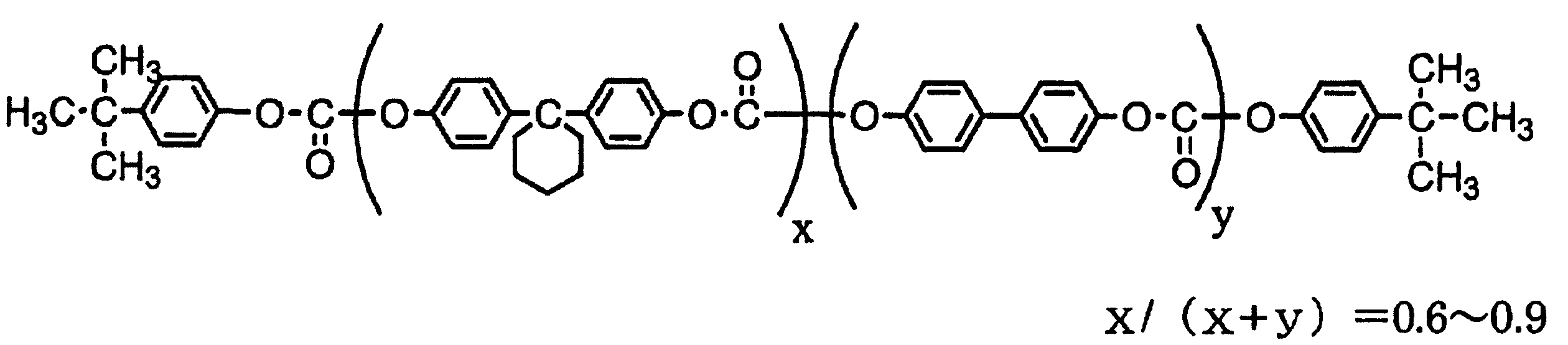
- the binder resin having a water vapor transmission rate in the range of 5 to 13 g / m 2 ⁇ day may include a resin having a repeating unit represented by the following formula (1). And a resin having a repeating unit represented by the following formula (2). Furthermore, the binder resin having a water vapor transmission rate in the range of 5 to 13 g / m 2 ⁇ day is represented by a resin having a repeating unit represented by the following formula (2) and a formula (3) below. A resin having a repeating unit may also be included. In the photoreceptor of the present invention, it is preferable that the charge generation material contains at least titanyl phthalocyanine. (1) (2) (3)
- a method for producing an electrophotographic photoreceptor according to a third aspect of the present invention is a method for producing the above electrophotographic photoreceptor, wherein the water vapor transmission rate is in the range of 5 to 13 g / m 2 ⁇ day.
- a layer containing a resin is formed using a dip coating method.
- An electrophotographic apparatus includes the above electrophotographic photoreceptor.
- the electrophotographic apparatus may be provided with a non-magnetic one-component contact development type cleaner-less process using polymerized toner.
- initial printing in a high-temperature and high-humidity environment is possible even when mounted on a high-speed monochrome high-speed machine or a tandem color machine equipped with a non-magnetic one-component contact development type cleaner-less process using polymerized toner.
- FIG. 2 is a schematic cross-sectional view showing a configuration example of a single-layer positively charged electrophotographic photoreceptor of the present invention.
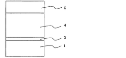
- FIG. 2 is a schematic cross-sectional view showing a configuration example of a laminated positively charged electrophotographic photoreceptor of the present invention.
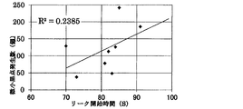
- It is a schematic block diagram which shows an example of the electrophotographic apparatus of this invention. It is a graph which shows the relationship between leak start time and the number of generation
- FIG. 1 and FIG. 2 are schematic cross-sectional views showing one structural example of the electrophotographic photoreceptor of the present invention.
- FIG. 1 shows a single-layer type positively charged electrophotographic photosensitive member having a single-layer type photosensitive layer 3 on a conductive support 1 with an undercoat layer 2 interposed therebetween, and
- FIG. A multilayer positively charged electrophotographic photoreceptor comprising a charge transport layer 4 and a charge generation layer 5 in order through an undercoat layer 2 is shown.
- the water vapor permeability of the binder resin contained in the outermost layer is in the range of 5 to 13 g / m 2 ⁇ day in both the single layer type and the multilayer type. In particular, it is preferably in the range of 6 to 12 g / m 2 ⁇ day.
- the water vapor transmission rate of the binder resin contained in the outermost layer is less than 5 g / m 2 ⁇ day, the adsorbed water tends to be unevenly distributed, and instead, the mixture of toner and paper powder tends to be fixed, resulting in 13 g. / M 2 ⁇ day, the film density decreases. Therefore, the resistance value decreases due to an increase in moisture content, the number of black spots and color spots increases due to the influence of discharge generated gas, and the fogging due to a decrease in charging potential. This will cause an image to be generated.
- the water vapor permeability of the binder resin contained in the outermost layer means the water vapor permeability of a mixture of two or more binder resins when two or more binder resins are contained. .
- the binder resin used in the present invention includes polycarbonate resins such as bisphenol A type, bisphenol Z type, and bisphenol A type-biphenyl copolymer, based on the dispersion stability and mechanical strength of the charge generation material used together.
- a resin is used as an essential component, and a desired water vapor transmission rate is obtained by mixing an appropriate amount of a resin having a higher water vapor transmission rate than a polycarbonate resin, for example, a polystyrene resin, a polyester resin, or a polyarylate resin. It is preferable.
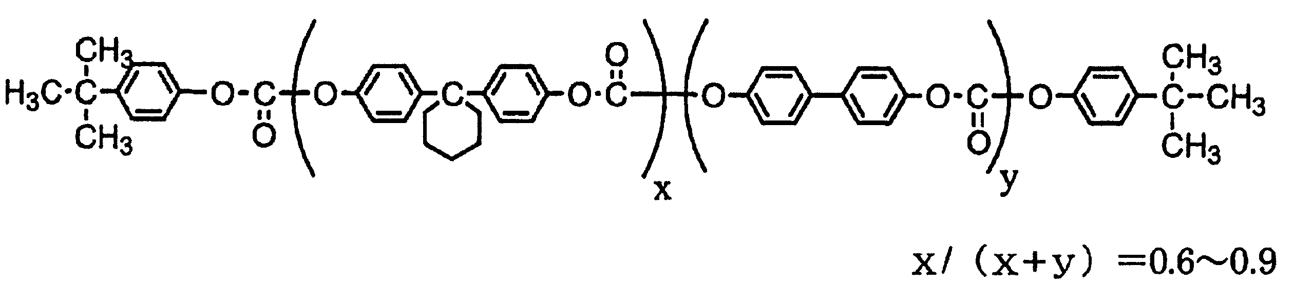
- a resin having a repeating unit represented by the following formula (1) can be suitably used, and a resin having a repeating unit represented by the following formula (1), and the following formula ( It is also preferable to use a resin having a repeating unit represented by 2) in combination. Moreover, it is also preferable to use together the polycarbonate-type resin which has a repeating unit represented by following formula (2), and the polyester resin which has a repeating unit represented by following formula (3).
- the conductive support 1 serves as one electrode of the photoconductor, and at the same time serves as a support for each layer constituting the photoconductor.
- the conductive support 1 may have any shape such as a cylindrical shape, a plate shape, or a film shape. In terms of material, a conductive treatment is applied to the surface of glass, resin or the like in addition to metals such as aluminum, stainless steel, and nickel. It may be given.
- the undercoat layer 2 is basically unnecessary in the present invention, but can be provided as necessary for the purpose of further improving the reliability.
- the undercoat layer 2 is composed of a resin-based layer or a metal oxide film such as alumite, for the purpose of improving the adhesion between the conductive support and the charge transport layer, and the charge injection property to the photosensitive layer. It is provided for the purpose of controlling.
- the resin material used for the undercoat layer include insulating polymers such as casein, polyvinyl alcohol, polyamide, melamine, and cellulose, and conductive polymers such as polythiophene, polypyrrole, and polyaniline. Alternatively, they can be used in combination as appropriate. These resins can also contain metal oxides such as titanium dioxide and zinc oxide.
- the single-layer type photosensitive layer 3 is mainly composed of a charge generation material, a hole transport material, an electron transport material, and a binder resin.
- the single-layer type photosensitive layer 3 may be formed on the outer periphery of the electrophotographic photoreceptor farthest from the conductive support 1.
- the electrophotographic photoreceptor may be mounted on the electrophotographic apparatus in a state where the surface of the photosensitive layer 3 farthest from the conductive support 1 can be in contact with the atmosphere.
- charge generation material As the charge generation material, X-type metal-free phthalocyanine alone, or ⁇ -type titanyl phthalocyanine, ⁇ -type titanyl phthalocyanine, Y-type titanyl phthalocyanine, ⁇ -type titanyl phthalocyanine, amorphous-type titanyl phthalocyanine, gallium phthalocyanine alone or in appropriate combination
- a suitable substance can be selected according to the light wavelength region of the exposure light source used for image formation. From the viewpoint of increasing sensitivity, titanyl phthalocyanine having high quantum efficiency is optimal.
- hole transport material As the hole transport material, various hydrazone compounds, styryl compounds, stilbene compounds, enamine compounds, diamine compounds, butadiene compounds, indole compounds, triphenylamine compounds, triphenyldiamine compounds and the like can be used alone or in appropriate combination. . Among these, styryl compounds containing a triphenylamine skeleton are preferable in terms of cost and performance.
- Electrode transport material As the electron transport material, a material having a high mobility is preferable, and a quinone material such as benzoquinone, stilbene quinone, naphthoquinone, dinaphthoquinone, diphenoquinone, phenanthrenequinone, and azoquinone, or a tetranaphthalenecarboxylic acid diimide material is preferable. These can be used alone or in combination with a binder resin to increase the content of the electron transporting material while suppressing precipitation, because of its injectability into the charge transporting layer and compatibility with the binder resin. preferable.
- a quinone material such as benzoquinone, stilbene quinone, naphthoquinone, dinaphthoquinone, diphenoquinone, phenanthrenequinone, and azoquinone, or a tetranaphthalenecarboxylic acid diimide material.
- Binder resin As described above, as the binder resin, various polycarbonate resins are essential, and any resin selected from polystyrene resins, polyester resins, polyarylate resins, and the like is used in appropriate combination in order to control the water vapor transmission rate. be able to.
- the photosensitive layer 3 can contain a deterioration inhibitor such as an antioxidant or a light stabilizer for the purpose of improving environmental resistance and stability against harmful light, as desired.
- a deterioration inhibitor such as an antioxidant or a light stabilizer for the purpose of improving environmental resistance and stability against harmful light, as desired.
- Compounds used for this purpose include chromanol derivatives such as tocopherol and esterified compounds, polyarylalkane compounds, hydroquinone derivatives, etherified compounds, dietherified compounds, benzophenone derivatives, benzotriazole derivatives, thioether compounds, phenylenediamine derivatives. Phosphonic acid ester, phosphite ester, phenol compound, hindered phenol compound, amine compound and the like.
- a leveling agent such as silicone oil or fluorine oil can be contained.
- metal oxides such as silicon oxide (silica), titanium oxide, zinc oxide, calcium oxide, aluminum oxide (alumina), zirconium oxide, etc. for the purpose of adjusting film hardness, reducing friction coefficient, and imparting lubricity
- metal sulfates such as barium sulfate and calcium sulfate, and metal nitride fine particles such as silicon nitride and aluminum nitride may be contained.
- other known additives can be contained as long as the electrophotographic characteristics are not significantly impaired.
- composition The mass ratio of the sum of the functional materials (charge generation material, electron transport material and hole transport material) in the photosensitive layer 3 to the binder resin is in the range of 45:55 to 55:45 in order to obtain desired characteristics. Is set. If the mass ratio of the functional material is more than 55% by mass in the photosensitive layer, that is, if the amount of the binder resin is less than 45% by mass, the amount of film loss increases, the durability decreases, and the glass transition point. The creep strength becomes insufficient due to the decrease in toner, and toner filming, external additives, and paper powder filming are likely to occur, and minute black spots due to adhesion of the mixture of toner and paper powder in a high temperature and high humidity environment like this time The generation amount of etc.
- the mass ratio of the functional material is less than 45% by mass in the photosensitive layer 3, that is, if the amount of the binder resin is more than 55% by mass, it is difficult to obtain desired sensitivity characteristics, which is suitable for practical use. There is a risk of disappearing. In general, from the viewpoint of suppressing member contamination, oil contamination, and sebum contamination while ensuring durability, it is desirable to increase the binder resin ratio.
- the content ratio of the charge generating material is preferably 0.5 to 3% by mass, more preferably 0.8 to 1.8% by mass of the entire film. If the amount of the charge generating material is too small, the sensitivity characteristics are insufficient, and the possibility of generation of interference fringes increases. If the amount is too large, the charging characteristics and fatigue characteristics (repetitive use stability) tend to be insufficient.
- the mass ratio of the electron transport material to the hole transport material can be changed in the range of 1: 1 to 1: 4. However, in general, in the range of 2: 3 to 1: 3, based on the transport balance of holes and electrons. It is more preferable to use it in terms of sensitivity characteristics, charging characteristics and fatigue characteristics.
- Solvents used for forming the photosensitive layer 3 include halogenated hydrocarbons such as dichloromethane, dichloroethane, chloroform, carbon tetrachloride, chlorobenzene; dimethyl ether, diethyl ether, tetrahydrofuran, dioxane, dioxolane, ethylene glycol dimethyl ether, diethylene glycol dimethyl ether, and the like. Ethers; ketones such as acetone, methyl ethyl ketone, and cyclohexanone can be used, and can be appropriately selected from the viewpoints of solubility, liquid stability, and coatability of various materials.
- the film thickness of the photosensitive layer 3 is preferably in the range of 15 to 40 ⁇ m, more preferably 20 to 35 ⁇ m, and even more preferably 25 to 30 ⁇ m from the viewpoint of securing practically effective performance.
- the conductive support 1 is the same as that of the single layer type photoreceptor.
- the undercoat layer 2 is the same as that of the single-layer type photoreceptor and is basically unnecessary in the present invention, but can be appropriately provided as necessary for improving the reliability.
- the charge transport layer 4 is mainly composed of a hole transport material and a binder resin.
- the hole transport material used for the charge transport layer 4 is the same as that of the single layer type photoreceptor, but from the viewpoint of smooth charge transfer from the charge generation layer 5 to the charge transport layer 4, It is desirable to use the same materials as included.
- Binder resin As the binder resin for the charge transport layer 4, the same resin as that of the single layer type can be used. However, since it is an inner layer, mechanical strength is not so required, while elution when the charge generation layer 5 is applied. Incompetence is required. From such a viewpoint, a resin that is difficult to elute in the solvent of the coating solution for forming the charge generation layer 5 is suitable, and a resin having a high molecular weight is preferably used. Further, in relation to the binder resin of the charge generation layer 5, it is preferable that the water vapor transmission rate of the binder resin of the charge transport layer 4 is lower than the water vapor transmission rate of the binder resin of the charge generation layer 5.
- the water vapor permeability of the binder resin of the charge transport layer 4 is preferably 4 g / m 2 ⁇ day or less, and more preferably 3 g / m 2 ⁇ day or less.
- the charge transport layer 4 may contain a deterioration inhibitor such as an antioxidant or a light stabilizer for the purpose of improving environmental resistance and stability against harmful light.
- a deterioration inhibitor such as an antioxidant or a light stabilizer for the purpose of improving environmental resistance and stability against harmful light.
- the same compounds as mentioned for the single-layer type photosensitive layer can be used.
- the charge transport layer 4 contains a leveling agent such as silicone oil or fluorine-based oil for the purpose of improving the leveling property of the formed film and imparting lubricity, as in the case of the single-layer type photosensitive layer. It can also be made. Furthermore, for the purpose of adjusting the film hardness, reducing the friction coefficient, imparting lubricity, etc., various metal oxides, metal sulfates and metal nitride fine particles similar to those mentioned for the single-layer type photosensitive layer are added. You may contain. Furthermore, if necessary, other known additives can be contained as long as the electrophotographic characteristics are not significantly impaired.
- a leveling agent such as silicone oil or fluorine-based oil for the purpose of improving the leveling property of the formed film and imparting lubricity, as in the case of the single-layer type photosensitive layer. It can also be made. Furthermore, for the purpose of adjusting the film hardness, reducing the friction coefficient, imparting lubricity, etc., various metal oxides, metal s
- the mass ratio of the hole transport material and the binder resin in the charge transport layer 4 can be in the range of 1: 3 to 3: 1 (25:75 to 75:25), and preferably 7:13. It is in the range of 13: 7 (35:65 to 65:35). If the content of the hole transport material is less than 25% by mass in the charge transport layer 4, generally the transport function is insufficient, the residual potential becomes high, and the environmental dependency of the exposed portion potential in the apparatus becomes large, Since the environmental stability of image quality deteriorates, it may not be suitable for use.
- the charge generation layer 5 is applied. There is a risk of adverse effects of elution.
- Solvents used for forming the charge transport layer 4 include halogenated hydrocarbons such as dichloromethane, dichloroethane, chloroform, carbon tetrachloride, chlorobenzene; dimethyl ether, diethyl ether, tetrahydrofuran, dioxane, dioxolane, ethylene glycol dimethyl ether, diethylene glycol dimethyl ether.
- Ethers such as acetone; ketones such as acetone, methyl ethyl ketone, and cyclohexanone can be used, and can be appropriately selected from the viewpoints of solubility, liquid stability, and coatability of various materials.
- the film thickness of the charge transport layer 4 is determined in view of the balance with the charge generation layer 5 described later, but from the viewpoint of ensuring practically effective performance, the range of 3 to 40 ⁇ m is preferable, and more preferably 5 to It is 30 ⁇ m, more preferably 7 to 20 ⁇ m.
- the charge generation layer 5 is formed by a method of applying a coating liquid in which particles of a charge generation material are dispersed in a binder resin in which a hole transport material and an electron transport material are dissolved.
- the charge generation layer 5 has a function of receiving light and generating carriers, and also has a function of transporting generated electrons to the surface of the photoreceptor and transporting holes to the charge transport layer 4.
- the charge generation layer 5 has high carrier generation efficiency, and at the same time, the injection property of the generated holes into the charge transport layer 4 is important.
- the charge generation layer 5 is less dependent on the electric field and preferably has a good injection even at a low electric field.
- the charge generation layer 5 may be formed on the outer periphery of the electrophotographic photoreceptor farthest from the conductive support 1.
- the charge transport layer 4 may be formed between the charge generation layer 5 and the conductive support 1.
- the electrophotographic photoreceptor may be mounted on the electrophotographic apparatus in a state where the surface of the charge generation layer 5 farthest from the conductive support 1 can be in contact with the atmosphere.
- charge generation material As the charge generation material, the same material as that of the single-layer type photoreceptor can be used, and a suitable substance can be selected according to the light wavelength region of the exposure light source used for image formation. From the viewpoint of increasing sensitivity, titanyl phthalocyanine having high quantum efficiency is optimal.
- the hole transport material preferably has a small difference in ionization potential from the hole transport material of the charge transport layer 4 because it is necessary to inject holes into the charge transport layer 4, specifically, within 0.5 eV. It is preferable that In particular, in the present invention, since the charge generation layer 5 is formed on the charge transport layer 4, the influence of elution of the charge transport layer 4 into the coating solution is suppressed when the charge generation layer 5 is applied, and the charge generation layer 5 is applied. In order to stabilize the liquid state of 5, it is preferable that the hole transport material contained in the charge transport layer 4 is also contained in the charge generation layer 5, and more preferably, the charge transport layer 4 and the charge generation layer 5. The same material is used as the hole transporting material used for.
- the electron transport material As the electron transport material, the same material as that of the single-layer type photoreceptor can be used, and a higher mobility material is preferable. However, from the injectability into the charge transport layer 4 and the compatibility with the binder resin, In addition to using alone, it is also preferable to increase the content of the electron transport material while suppressing precipitation using two or more materials.
- Binder resin As the binder resin for the charge generation layer 5, as in the case of the single-layer type photoreceptor, various polycarbonate resins are essential, and in order to control the water vapor transmission rate, polystyrene resins, polyester resins and polyarylate resins are used. Arbitrary resins selected from the above can be used in appropriate combination.
- the binder resin contained in the transport layer 4 is also contained in the charge generation layer 5, and more preferably, the same resin is used as the binder resin used in the charge transport layer 4 and the charge generation layer 5.
- the charge generation layer 5 may contain a deterioration inhibitor such as an antioxidant or a light stabilizer for the purpose of improving the environmental resistance and the stability against harmful light, as desired.
- a deterioration inhibitor such as an antioxidant or a light stabilizer for the purpose of improving the environmental resistance and the stability against harmful light, as desired.
- the compound used for such a purpose the same compounds as mentioned for the single-layer type photosensitive layer can be used.
- the charge generation layer 5 contains a leveling agent such as silicone oil or fluorine-based oil for the purpose of improving the leveling property of the formed film and imparting lubricity, as in the case of the single-layer type photosensitive layer. It can also be made. Furthermore, for the purpose of adjusting the film hardness, reducing the friction coefficient, imparting lubricity, etc., various metal oxides, metal sulfates and metal nitride fine particles similar to those mentioned for the single-layer type photosensitive layer are added. You may contain. Furthermore, if necessary, other known additives can be contained as long as the electrophotographic characteristics are not significantly impaired.
- a leveling agent such as silicone oil or fluorine-based oil for the purpose of improving the leveling property of the formed film and imparting lubricity, as in the case of the single-layer type photosensitive layer. It can also be made. Furthermore, for the purpose of adjusting the film hardness, reducing the friction coefficient, imparting lubricity, etc., various metal oxides, metal s
- the distribution amount of each functional material (charge generation material, electron transport material, and hole transport material) in the charge generation layer 5 is set as follows.
- the content of the charge generation material in the charge generation layer 5 is 1 to 3.0% by mass, particularly 1.5 to 2.5% by mass in the charge generation layer 5. preferable.
- the mass ratio of the sum of the functional materials (charge generation material, electron transport material, and hole transport material) and the binder resin in the charge generation layer 5 has the desired characteristics as in the case of the single layer type photoreceptor.
- the mass ratio of the functional material is larger than 65 mass% in the charge generation layer 5, that is, the amount of the binder resin is smaller than 35 mass%.
- the durability decreases, and the creep strength is insufficient due to the decrease in the glass transition point, making it easy for toner filming, external additives, and paper powder filming to occur.
- the amount of fine black spots generated due to the adhering of the mixture of toner and paper powder increases.
- contact member contamination creep deformation
- contamination due to grease such as grease and sebum contamination are also deteriorated.
- the mass ratio of the functional material is less than 35 mass% in the charge generation layer 5, that is, if the amount of the binder resin is greater than 65 mass%, it is difficult to obtain desired sensitivity characteristics. May not be suitable. In general, from the viewpoint of suppressing member contamination, oil contamination and sebum contamination while ensuring durability, it is desirable to increase the binder resin ratio.
- the mass ratio of the electron transport material and the hole transport material can be changed in the range of 1: 5 to 5: 1.
- the charge transport having a hole transport function is provided below the charge generation layer 5. Since layer 4 is present, 5: 1 to 4: as opposed to a 1: 5 to 2: 4 hole-transporting material rich composition, which is a typical mass ratio range for single layer organic photoreceptors.
- the range of 2 is suitable, and in particular, the range of 4: 1 to 3: 2 is more preferred in terms of overall characteristics.
- the content of the hole transporting material which is one factor of generation of cracks due to sebum adhesion, can be suppressed to be low.
- Solvents used to form the charge generation layer 5 include halogenated hydrocarbons such as dichloromethane, dichloroethane, chloroform, carbon tetrachloride, chlorobenzene; dimethyl ether, diethyl ether, tetrahydrofuran, dioxane, dioxolane, ethylene glycol dimethyl ether, diethylene glycol dimethyl ether. Ethers such as acetone; ketones such as acetone, methyl ethyl ketone, and cyclohexanone. Of these, those having a high boiling point are generally preferred. Specifically, those having a boiling point of 60 ° C. or higher, particularly those having a boiling point of 80 ° C.
- titanyl phthalocyanine having a high quantum efficiency is used as a charge generation material for high sensitivity
- 1,2-dichloroethane having a specific gravity of 1 or more and a boiling point of 70 ° C. or more is used to form a charge generation layer. It is preferable to use it as a solvent used in the above in view of dispersion stability and difficulty in elution of the charge transport layer.
- the film thickness of the charge generation layer 5 is determined in view of the balance with the charge transport layer 4, but from the viewpoint of ensuring practically effective performance, a range of 3 ⁇ m to 40 ⁇ m is preferable, and preferably 5 ⁇ m to 30 ⁇ m. More preferably, the thickness is 10 ⁇ m to 18 ⁇ m.
- a layer containing a binder resin having a water vapor permeability in the range of 5 to 13 g / m 2 ⁇ day is formed using a dip coating method.
- the layer containing a binder resin having a water vapor transmission rate in the range of 5 to 13 g / m 2 ⁇ day is a single-layer type photosensitive layer 3 in the case of a single-layer type photoreceptor, In this case, the charge generation layer 5 is used.
- the electrophotographic apparatus of the present invention is equipped with the above photoreceptor, and in particular, a high-speed monochrome high-speed machine or tandem having a non-magnetic one-component contact developing type cleaner-less process using polymerized toner. It is suitably applied to a color machine.
- non-contact charging method using scorotron non-magnetic one-component contact development method using suspension polymerization toner, and high transfer efficiency. Only the toner is collected, and the untransferred toner is suitable as an electrophotographic apparatus using a process in which the toner is collected at the developing unit.
- the amount of abrasion of the photosensitive layer is small, and in particular, substances that do not have a charge once attached are difficult to remove.
- the process is easy to adhere.
- FIG. 3 shows a schematic configuration diagram of an example of the electrophotographic apparatus of the present invention.
- the illustrated electrophotographic apparatus 60 includes an electrophotographic photoreceptor 7 including the conductive support 1 and the photosensitive layer 300 coated on the outer periphery thereof. More specifically, the illustrated electrophotographic apparatus 60 includes a charger 21 such as a roller charging member disposed on the outer peripheral edge of the photoreceptor 7, a high-voltage power supply 22 that supplies an applied voltage to the charger 21, an image An exposure member 23, a developing device 24 including a developing roller 241, a paper feeding member 25 including a paper feeding roller 251 and a paper feeding guide 252, a transfer charger (direct charging type) 26, and a paper dust collecting unit 27. And a color printer.
- a charger 21 such as a roller charging member disposed on the outer peripheral edge of the photoreceptor 7, a high-voltage power supply 22 that supplies an applied voltage to the charger 21, an image An exposure member 23, a developing device 24 including a developing roller 241, a paper feeding member 25 including
- conductive support there are two types of shapes of ⁇ 30 mm ⁇ length 244.5 mm and ⁇ 30 mm ⁇ length 254.4 mm, and aluminum 0.75 mm meat cut to a surface roughness (Rmax) of 0.2 ⁇ m. Thick tubes were used.
- hole transport material As the hole transport material, the following compounds H1, H2, and H3 were used.
- Electron transport material As the electron transport material, the following compounds E1, E2 and E3 were used.
- B2 Polycarbonate resin (water vapor transmission rate: 6.08 g / m 2 ⁇ day)
- B4 Polycarbonate resin (water vapor transmission rate: 2.08 g / m 2 ⁇ day)
- the following resins B7 to B10 were also used as optional resins used in combination with any of the polycarbonate resins B1 to B6.
- B7 General-purpose polystyrene resin GPPS manufactured by Toyo Engineering Co., Ltd. (water vapor transmission rate: 30.0 g / m 2 ⁇ day)
- B8 General-purpose polymer polyester resin Byron 290 manufactured by Toyobo Co., Ltd.
- B9 Polymer polyester resin having the following repeating units (water vapor transmission rate: 7.5 g / m 2 ⁇ day) a ⁇ b ⁇ c ⁇ d ⁇ 25 mol% (3)
- B10 General-purpose polyarylate resin U polymer manufactured by Unitika Ltd. (water vapor permeability 12.1 g / m 2 ⁇ day)
- antioxidant hindered phenol antioxidant dibutylhydroxytoluene (BHT) was used.
- BHT hindered phenol antioxidant dibutylhydroxytoluene
- dimethyl silicone oil KF-54 manufactured by Shin-Etsu Chemical was used.
- ⁇ Coating solution for laminated type photoreceptor> "Coating liquid for charge transport layer”
- the hole transport material, binder resin, and additive material were added to a container together with a solvent at a predetermined mixing ratio and dissolved to prepare a charge transport layer coating solution for a multilayer photoreceptor.
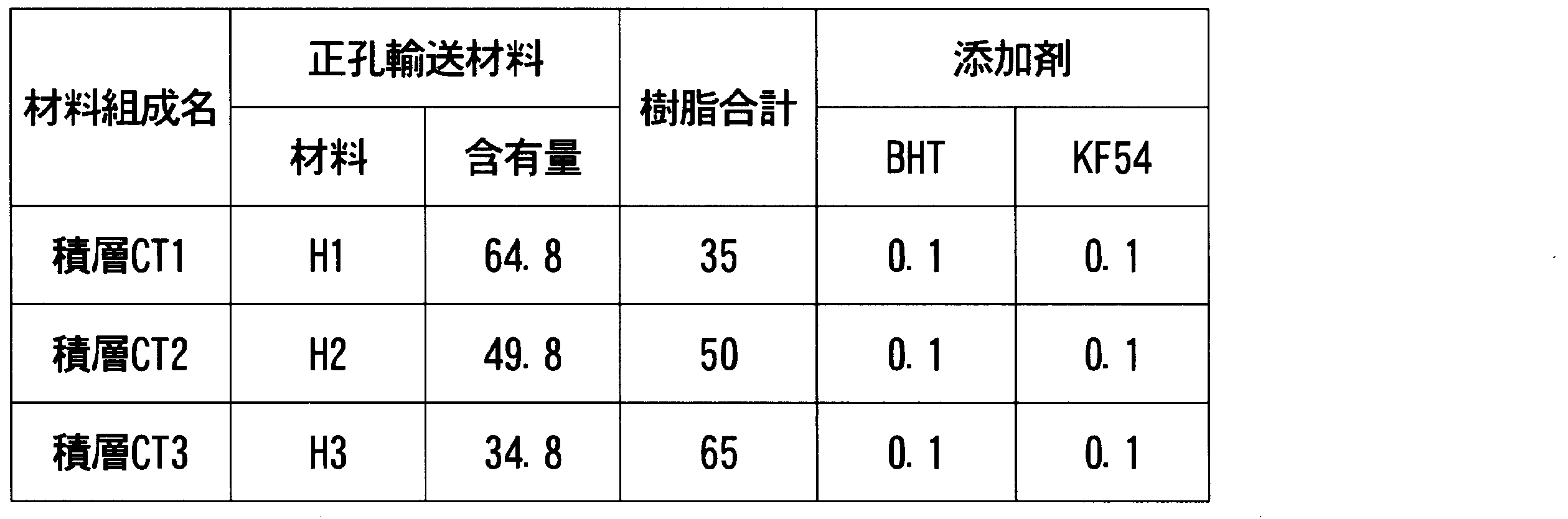
- the composition ratio of materials other than the binder resin is shown in Table 2 below. Content in a table
- surface shows the mass%. Further, as the binder resin, the resin B5 was used.
- Coating solution for charge generation layer The hole transport material, electron transport material, binder resin and additive material were added to a container together with a solvent at a predetermined mixing ratio and dissolved. Next, the charge generation material weighed so as to have a predetermined weight ratio was added and dispersed with a dyno mill (MULTILAB of Shinmaru Enterprise Co., Ltd.) to prepare a charge generation layer coating solution for a multilayer photoreceptor.
- the composition ratio of materials other than the binder resin is shown in Table 3 below. Content in a table
- the coating solution for the single-layer type photoconductors having the material compositions GT2 and GT3 shown in Table 1 above was changed in the binder resin as shown in Examples 24 and 25 in Table 5 below, so that The film was dip-coated and dried with hot air at 110 ° C. for 60 minutes to form single-layer type photosensitive layers having a film thickness of 20 ⁇ m and 35 ⁇ m, and a single-layer type photoreceptor was produced.
- the charge transport layer coating solution having the material composition CT1 shown in Table 2 above is dip-coated on the conductive support and dried in hot air at 110 ° C. for 60 minutes, so that three types of film thicknesses of 7 ⁇ m, 10 ⁇ m, and 20 ⁇ m A charge transport layer was formed.
- the charge generation layer coating solution having the material composition G1 shown in Table 3 above is dip-coated by changing the binder resin as shown in Tables 6 and 7 below, followed by drying with hot air at 110 ° C. for 60 minutes.
- Examples 26 to 35 and Comparative Examples 16 to 24 had a thickness of 20 ⁇ m
- Examples 36 to 40 and Comparative Examples 25 and 26 had a thickness of 27 ⁇ m
- Examples 41 to 48 and Comparative Examples 27 to 30 had a thickness of 35 ⁇ m.
- the charge transport layer coating solution having the material composition CT1 shown in Table 2 above is dip coated on the conductive support and dried with hot air at 110 ° C. for 60 minutes, whereby the charge transport layer having a thickness of 7 ⁇ m and 20 ⁇ m is obtained.
- the binder resin was replaced with Example 49, Comparative Example 31 and Example in Table 7 using G2 and G3 charge generation layer coating solutions instead of the material composition G1 shown in Table 3 above.
- 50 modified as shown in Comparative Example 32, dip-coated, dried by hot air at 110 ° C. for 60 minutes to form charge generation layers having a film thickness of 13 ⁇ m and 15 ⁇ m, and the total film thickness was 20 ⁇ m respectively. And a 35 ⁇ m multilayer photoreceptor.
- the charge transport layer coating liquids of CT2 and CT3 are dip coated on the conductive support and dried with hot air at 110 ° C. for 60 minutes to obtain a film thickness of 7 ⁇ m.
- the charge generation layer coating solution of material composition G1 shown in Table 3 above was changed as shown in Examples 51 and 52 in Table 7 below. Immersion coating was performed, and hot-air drying at 110 ° C. for 60 minutes was performed to form charge generation layers having a film thickness of 13 ⁇ m and 15 ⁇ m, so that laminated photoreceptors having a total film thickness of 20 ⁇ m and 35 ⁇ m were produced.
- the charge transport layer coating solution a material in which the binder resin is changed as shown in Example 53 in Table 8 below in the material composition CT1 shown in Table 2 above is used on the conductive support.
- the film was dip coated and dried with hot air at 110 ° C. for 60 minutes to form a 7 ⁇ m thick charge transport layer.
- the charge generation layer coating solution having the material composition G1 shown in Table 3 above was dip-coated by changing the binder resin as shown in Example 53 in Table 8 below, and heated at 110 ° C. for 60 minutes. Drying was performed to form a 13 ⁇ m-thick charge generation layer to produce a laminated photoreceptor having a total thickness of 20 ⁇ m.
- the charge transport layer coating solution a material in which the binder resin is changed as shown in Example 54 of Table 8 below in the material composition CT1 shown in Table 2 above is used on the conductive support.
- the film was dip coated and dried with hot air at 110 ° C. for 60 minutes to form a charge transport layer having a thickness of 20 ⁇ m.
- the charge generation layer coating solution having the material composition G3 shown in Table 3 above was dip-coated by changing the binder resin as shown in Example 54 in Table 8 below, and hot air at 110 ° C. for 60 minutes was applied. Drying was performed to form a charge generation layer having a film thickness of 15 ⁇ m, and a laminated photoreceptor having a total film thickness of 35 ⁇ m was prepared.
- the charge transport layer coating solution a material in which the binder resin is changed as shown in Example 55 in Table 8 below in the material composition CT2 shown in Table 2 above is used on the conductive support. Immersion coating was performed and hot air drying was performed at 110 ° C. for 60 minutes to form a 10 ⁇ m-thick charge transport layer.
- the charge generation layer coating solution having the material composition G1 shown in Table 3 above was dip-coated by changing the binder resin as shown in Example 55 in Table 8 below, and hot air at 110 ° C. for 60 minutes was applied. Drying was performed to form a charge generation layer having a film thickness of 17 ⁇ m, and a laminated photoreceptor having a total film thickness of 27 ⁇ m was prepared.
- the coating liquid for the charge transport layer the conductive support described above was used by changing the binder resin as shown in Examples 56 and 57 in Table 8 below in the material composition CT3 shown in Table 2 above.
- a charge transport layer having a film thickness of 10 ⁇ m was formed by dip coating on the substrate and drying with hot air at 110 ° C. for 60 minutes.
- the charge generation layer coating solution having the material composition G1 shown in Table 3 above was dip-coated by changing the binder resin as shown in Examples 56 and 57 in Table 8 below, and 110 ° C. for 60 minutes.
- a charge generation layer having a film thickness of 17 ⁇ m was formed to produce a laminated photoreceptor having a total film thickness of 27 ⁇ m.
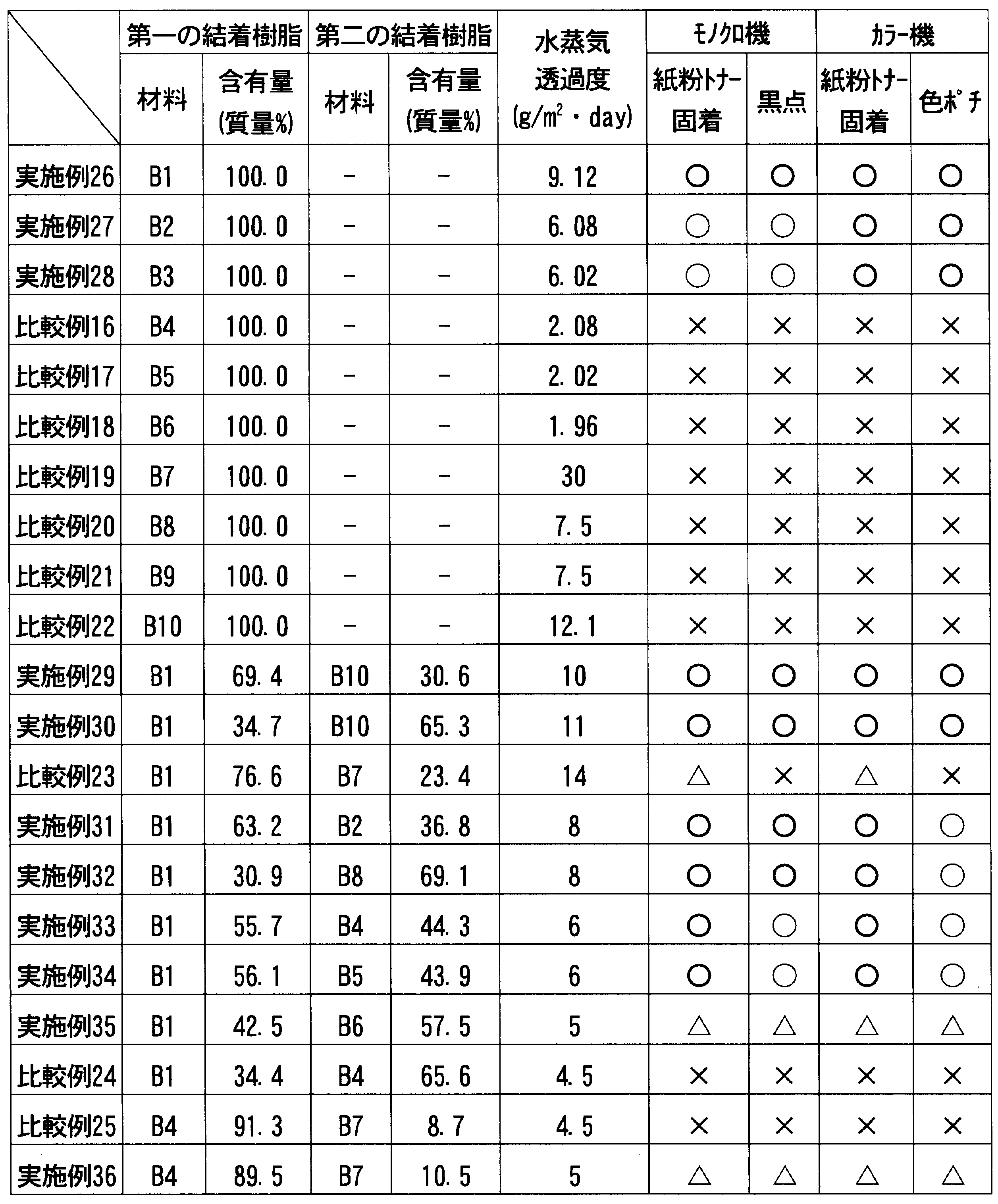
- ⁇ Evaluation of occurrence of black spots or color spots The number of small black spots or color spots (having a diameter of about 0.5 mm or less) in the white paper portion was measured in the photosensitive member cycle. Three-stage evaluation was performed as follows. ⁇ : 5 or less, ⁇ : 6-20, ⁇ : 21 or more
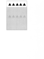
- FIG. 5 The image in FIG. 5 is a 600 dpi image, and a solid image (filled triangle) of ⁇ is arranged in a horizontal direction in a solid white image at the top, and a stipple image of 1 dot and 2 spaces at the bottom: halftone (H / T) It is the ghost evaluation image which arranged the image.
- the ghost image in this case means that a portion having a higher density than the peripheral portion is formed in the shape of ⁇ on the H / T image.
Landscapes
- Physics & Mathematics (AREA)
- General Physics & Mathematics (AREA)
- Spectroscopy & Molecular Physics (AREA)
- Chemical & Material Sciences (AREA)
- Chemical Kinetics & Catalysis (AREA)
- Health & Medical Sciences (AREA)
- Medicinal Chemistry (AREA)
- Polymers & Plastics (AREA)
- Organic Chemistry (AREA)
- Photoreceptors In Electrophotography (AREA)
- Developing Agents For Electrophotography (AREA)
Abstract
Description
前記結着樹脂がポリカーボネート系樹脂を含むとともに、前記結着樹脂の水蒸気透過率が、5~13g/m2・dayの範囲であるものである。
前記電荷発生層の結着樹脂がポリカーボネート系樹脂を含むとともに、前記電荷発生層の結着樹脂の水蒸気透過率が、5~13g/m2・dayの範囲であるものである。



[導電性支持体]
導電性支持体1は、感光体の一電極としての役目を担うのと同時に、感光体を構成する各層の支持体ともなっている。導電性支持体1は、円筒状や板状、フィルム状などのいずれの形状でもよく、材質的には、アルミニウムやステンレス鋼、ニッケルなどの金属類の他、ガラスや樹脂などの表面に導電処理を施したものでもよい。
下引き層2は、本発明において基本的には不要であるが、信頼性をさらに向上させる目的で、必要に応じ設けることができる。下引き層2は、樹脂を主成分とする層や、アルマイトなどの金属酸化皮膜からなり、導電性支持体と電荷輸送層との密着性を向上する目的や、感光層への電荷の注入性を制御する目的で、設けられる。下引き層に用いられる樹脂材料としては、カゼインやポリビニルアルコール、ポリアミド、メラミン、セルロースなどの絶縁性高分子、および、ポリチオフェンやポリピロール、ポリアニリンなどの導電性高分子が挙げられ、これらの樹脂は単独、あるいは適宜組み合わせて混合して用いることができる。また、これらの樹脂に、二酸化チタンや酸化亜鉛などの金属酸化物を含有させることもできる。
単層型の感光層3は、主として、電荷発生材料、正孔輸送材料、電子輸送材料および結着樹脂よりなる。ここで、単層型の感光層3は、導電性支持体1から最も離れた、電子写真用感光体の外周に形成されてよい。また、電子写真用感光体は、導電性支持体1から最も離れた、感光層3の表面が大気に接触し得る状態で、電子写真装置に搭載されてよい。
電荷発生材料としては、X型無金属フタロシアニンを単独、若しくは、α型チタニルフタロシアニン、β型チタニルフタロシアニン、Y型チタニルフタロシアニン、γ型チタニルフタロシアニン、アモルファス型チタニルフタロシアニン、ガリウムフタロシアニンを単独、または適宜組合せて用いることができ、画像形成に使用される露光光源の光波長領域に応じて好適な物質を選ぶことができる。高感度化の観点からは、量子効率の高いチタニルフタロシアニンが最適である。
正孔輸送材料としては、各種ヒドラゾン化合物やスチリル化合物、スチルベン化合物、エナミン化合物、ジアミン化合物、ブタジエン化合物、インドール化合物、トリフェニルアミン化合物、トリフェニルジアミン化合物等を単独、あるいは適宜組合せて用いることができる。中でも、トリフェニルアミン骨格を含むスチリル系化合物が、コストおよび性能面で好適である。
電子輸送材料としては、高移動度の材料であるほど好ましく、ベンゾキノンやスチルベンキノン、ナフトキノン、ジナフトキノン、ジフェノキノン、フェナントレンキノン、アゾキノン等のキノン系材料、あるいは、テトラナフタレンカルボン酸ジイミド系材料が好ましい。これらは、電荷輸送層への注入性や結着樹脂との相溶性から、単独で用いる他、2種以上の材料を用いて、析出を抑えつつ、電子輸送材料の含有量を増加させることも好ましい。
結着樹脂は、上述したように、各種ポリカーボネート系樹脂を必須とし、水蒸気透過率を制御するため、ポリスチレン系樹脂、ポリエステル系樹脂やポリアリレート系樹脂などから選択される任意樹脂を適宜組み合わせて用いることができる。
感光層3中には、所望に応じ、耐環境性や有害な光に対する安定性を向上させる目的で、酸化防止剤や光安定剤などの劣化防止剤を含有させることができる。このような目的に用いられる化合物としては、トコフェロールなどのクロマノール誘導体およびエステル化化合物、ポリアリールアルカン化合物、ハイドロキノン誘導体、エーテル化化合物、ジエーテル化化合物、ベンゾフェノン誘導体、ベンゾトリアゾール誘導体、チオエーテル化合物、フェニレンジアミン誘導体、ホスホン酸エステル、亜リン酸エステル、フェノール化合物、ヒンダードフェノール化合物、アミン化合物等が挙げられる。
感光層3内の機能材料(電荷発生材料、電子輸送材料および正孔輸送材料)の和と結着樹脂との質量比率は、所望の特性を得るために45:55~55:45の範囲で設定される。機能材料の質量比率が、感光層中の55質量%より多く、すなわち、結着樹脂の量が45質量%より少ないと、膜減り量が大きくなって、耐久性が低下する他、ガラス転移点の低下によりクリープ強度が不足して、トナーフィルミングや外部添加材、紙粉のフィルミングが起きやすくなり、今回のような高温高湿環境下でのトナーおよび紙粉の混合物の固着による微小黒点等の発生量が大きくなる。加えて、接触部材汚染(クリープ変形)が生じ易くなり、グリス等の油脂による汚染性や皮脂汚染性も悪化する。また、上記機能材料の質量比率が、感光層3中の45質量%より少なく、すなわち、結着樹脂の量が55質量%より多いと、所望の感度特性を得ることが困難となり、実用に適さなくなるおそれがある。一般に、耐久性を確保しつつ、部材汚染、油脂汚染および皮脂汚染を抑制する観点からは、結着樹脂比率は高くすることが望ましい。
感光層3を形成する際に用いられる溶剤としては、ジクロロメタン、ジクロロエタン、クロロホルム、四塩化炭素、クロロベンゼン等のハロゲン化炭化水素;ジメチルエーテル、ジエチルエーテル、テトラヒドロフラン、ジオキサン、ジオキソラン、エチレングリコールジメチルエーテル、ジエチレングリコールジメチルエーテル等のエーテル類;アセトン、メチルエチルケトン、シクロヘキサノン等のケトン類等が挙げられ、各種材料の溶解性、液安定性および塗工性の観点より適宜選択することができる。
感光層3の膜厚は、実用上有効な性能を確保する観点より15~40μmの範囲が好適であり、より好適には20~35μmであり、さらに好適には25~30μmである。
[導電性支持体]
導電性支持体1については、単層型感光体と同様である。
下引き層2についても、単層型感光体と同様であり、本発明において基本的には不要であるが、信頼性向上のため、必要に応じて適宜設けることが可能である。
電荷輸送層4は、主として正孔輸送材料と結着樹脂とにより構成される。
電荷輸送層4に使用される正孔輸送材料としては、単層型感光体と同様であるが、電荷発生層5から電荷輸送層4への円滑な電荷移動の観点より、電荷発生層5に含まれる材料と同じものを用いることが望ましい。
電荷輸送層4の結着樹脂としては、単層型と同様のものを用いることができるが、内側の層であることから機械強度があまり要求されない一方、電荷発生層5を塗布した際の溶出しにくさが要求される。このような観点から、電荷発生層5の形成用の塗布液の溶剤に溶出しにくい樹脂が好適であり、分子量も高い樹脂を用いることが好ましい。また、電荷発生層5の結着樹脂との関係では、電荷輸送層4の結着樹脂の水蒸気透過率が、電荷発生層5の結着樹脂の水蒸気透過率よりも低いことが好ましい。放電生成ガスが電荷輸送層4に浸入すると劣化が生じやすいので、電荷輸送層4の水蒸気透過率をより低く抑えることが、劣化防止の点で有効である。具体的には、電荷輸送層4の結着樹脂の水蒸気透過率は、4g/m2・day以下とすることが好ましく、3g/m2・day以下とすることがより好ましい。
電荷輸送層4中には、所望に応じ、耐環境性や有害な光に対する安定性を向上させる目的で、酸化防止剤や光安定剤などの劣化防止剤を含有させることができる。このような目的に用いられる化合物としては、単層型感光層について挙げたのと同様の化合物を用いることができる。
電荷輸送層4における正孔輸送材料と結着樹脂との質量比率は、1:3~3:1(25:75~75:25)の範囲とすることができ、好適には、7:13~13:7(35:65~65:35)の範囲である。正孔輸送材料の含有量が、電荷輸送層4中の25質量%より少ないと、一般に輸送機能が不足し、残留電位が高くなる他、装置内の露光部電位の環境依存性が大きくなり、画像品質の環境安定性が悪化してしまうので、使用に適さなくなるおそれがある。一方、正孔輸送材料の含有量が、電荷輸送層4中の75質量%より多くなり、すなわち、結着樹脂が電荷輸送層4中の25質量%より少なくなると、電荷発生層5を塗布した際の溶出の弊害が発生するおそれがある。
電荷輸送層4を形成する際に用いられる溶剤としては、ジクロロメタン、ジクロロエタン、クロロホルム、四塩化炭素、クロロベンゼン等のハロゲン化炭化水素;ジメチルエーテル、ジエチルエーテル、テトラヒドロフラン、ジオキサン、ジオキソラン、エチレングリコールジメチルエーテル、ジエチレングリコールジメチルエーテル等のエーテル類;アセトン、メチルエチルケトン、シクロヘキサノン等のケトン類等が挙げられ、各種材料の溶解性、液安定性および塗工性の観点より、適宜選択することができる。
電荷輸送層4の膜厚は、後述する電荷発生層5との兼ね合いで決められるが、実用上有効な性能を確保する観点より、3~40μmの範囲が好適であり、より好適には5~30μm、さらに好適には7~20μmである。
電荷発生層5は、電荷発生材料の粒子を、正孔輸送材料および電子輸送材料が溶解した結着樹脂中に分散させた塗布液を塗布するなどの方法により形成される。電荷発生層5は、光を受容してキャリアを発生する機能をもつとともに、発生した電子を感光体表面に運び、正孔を上記電荷輸送層4に運ぶ機能を有する。電荷発生層5は、キャリアの発生効率が高いことと同時に、発生した正孔の電荷輸送層4への注入性が重要であり、電場依存性が少なく、低電場でも注入の良いことが望ましい。ここで、電荷発生層5は、導電性支持体1から最も離れた、電子写真用感光体の外周に形成されてよい。電荷輸送層4は、電荷発生層5と導電性支持体1との間に形成されてよい。また、電子写真用感光体は、導電性支持体1から最も離れた、電荷発生層5の表面が大気に接触し得る状態で、電子写真装置に搭載されてよい。
電荷発生材料としては、単層型感光体と同様のものを用いることができ、画像形成に使用される露光光源の光波長領域に応じて好適な物質を選ぶことができる。高感度化の観点からは、量子効率の高いチタニルフタロシアニンが最適である。
正孔輸送材料としては、電荷輸送層4に正孔を注入する必要上、電荷輸送層4の正孔輸送材料とのイオン化ポテンシャルの差異が小さいことが好ましく、具体的には、0.5eV以内であることが好ましい。特に、本発明において、電荷発生層5は電荷輸送層4上に塗布形成されるので、電荷発生層5の塗布時に、電荷輸送層4の塗布液への溶出の影響を抑えて、電荷発生層5の液状態を安定化させるために、電荷輸送層4に含まれる正孔輸送材料が電荷発生層5にも含まれていることが好ましく、より好ましくは、電荷輸送層4および電荷発生層5に用いる正孔輸送材料として、同じものを使用する。
電子輸送材料としては、単層型感光体と同様のものを用いることができ、高移動度の材料であるほど好ましいが、電荷輸送層4への注入性や結着樹脂との相溶性から、単独で用いる他、2種以上の材料を用いて、析出を抑えつつ、電子輸送材料の含有量を増加させることも好ましい。
電荷発生層5の結着樹脂としては、単層型感光体の場合と同様に、各種ポリカーボネート系樹脂を必須とし、水蒸気透過率を制御するため、ポリスチレン系樹脂、ポリエステル系樹脂やポリアリレート系樹脂などから選択される任意樹脂を適宜組み合わせて用いることができる。特には、上記正孔輸送材料と同様に、電荷発生層5の塗布時に電荷輸送層4の塗布液への溶出の影響を抑えて、電荷発生層5の液状態を安定化するために、電荷輸送層4に含まれる結着樹脂が電荷発生層5にも含まれていることが好ましく、より好ましくは、電荷輸送層4および電荷発生層5で用いる結着樹脂として、同じものを使用する。
電荷発生層5中には、所望に応じ、耐環境性や有害な光に対する安定性を向上させる目的で、酸化防止剤や光安定剤などの劣化防止剤を含有させることができる。このような目的に用いられる化合物としては、単層型感光層について挙げたのと同様の化合物を用いることができる。
電荷発生層5における各々の機能材料(電荷発生材料、電子輸送材料および正孔輸送材料)の配分量については、以下のように設定される。まず、本発明においては、電荷発生層5中の電荷発生材料の含有率が、電荷発生層5中の1~3.0質量%、特には1.5~2.5質量%であることが好ましい。また、電荷発生層5における機能材料(電荷発生材料、電子輸送材料および正孔輸送材料)の和と結着樹脂との質量比率は、単層型感光体の場合と同様に、所望の特性を得るために35:65~65:35の範囲で設定されるが、機能材料の質量比率が、電荷発生層5中の65質量%より多く、すなわち、結着樹脂の量が35質量%より少ないと、膜減り量が大きくなって、耐久性が低下する他、ガラス転移点の低下によりクリープ強度が不足して、トナーフィルミングや外部添加材、紙粉のフィルミングが起きやすくなり、今回のような高温高湿環境下でのトナーおよび紙粉の混合物の固着による微小黒点等の発生量が大きくなる。加えて、接触部材汚染(クリープ変形)が生じ易くなり、グリス等の油脂による汚染性、皮脂汚染性も悪化する。また、上記機能材料の質量比率が、電荷発生層5中の35質量%より少なく、すなわち、結着樹脂の量が65質量%より多いと、所望の感度特性を得ることが困難となり、実用に適さなくなるおそれがある。一般に、耐久性を確保しつつ、部材汚染、油脂汚染および皮脂汚染を抑制する観点からは、結着樹脂比率を高くすることが望ましい。
電荷発生層5を形成するために用いられる溶剤としては、ジクロロメタン、ジクロロエタン、クロロホルム、四塩化炭素、クロロベンゼン等のハロゲン化炭化水素;ジメチルエーテル、ジエチルエーテル、テトラヒドロフラン、ジオキサン、ジオキソラン、エチレングリコールジメチルエーテル、ジエチレングリコールジメチルエーテル等のエーテル類;アセトン、メチルエチルケトン、シクロヘキサノン等のケトン類等が挙げられる。このうち、一般的に、沸点が高いものが好ましく、具体的には沸点が60℃以上のもの、特には沸点が80℃以上のものを用いることが好適である。中でも、高感度化のために高量子効率のチタニルフタロシアニンを電荷発生材料に用いた場合には、比重が1以上で沸点が70℃以上の1,2-ジクロロエタンを、電荷発生層を形成する際に用いる溶媒として用いることが、分散安定性および電荷輸送層の溶出しにくさの点で好適である。
電荷発生層5の膜厚は、電荷輸送層4との兼ね合いで決められるが、実用上有効な性能を確保する観点より、3μm~40μmの範囲が好適であり、好適には5μm~30μmであり、より好適には10μm~18μmである。
本発明の感光体を製造するに際しては、上記水蒸気透過率が5~13g/m2・dayの範囲である結着樹脂を含む層を、浸漬塗工法を用いて製膜する。浸漬塗工法を用いることで、外観品質が良好で電気特性の安定した感光体を、低コストかつ高生産性を確保しつつ製造することができる。上記水蒸気透過率が5~13g/m2・dayの範囲である結着樹脂を含む層とは、単層型感光体の場合には単層型の感光層3であり、積層型感光体の場合には電荷発生層5である。本発明の感光体を製造するに際して、浸漬塗工法を用いる以外の点については、特に制限はなく、常法に従い行うことができる。
本発明の電子写真装置は、上記感光体を搭載してなるものであり、特には、重合トナーを用いた非磁性一成分接触現像方式のクリーナーレスプロセスを備える高画像品質なモノクロ高速機やタンデムカラー機に好適に適用される。
導電性支持体としては、φ30mm×長さ244.5mmおよびφ30mm×長さ254.4mmの2種類の形状で、表面粗さ(Rmax)0.2μmに切削加工されたアルミニウム製の0.75mm肉厚管を用いた。
(電荷発生材料)
電荷発生材料としては、下記構造式で示されるチタニルフタロシアニンG1を用いた。

正孔輸送材料としては、下記化合物H1、H2およびH3を用いた。
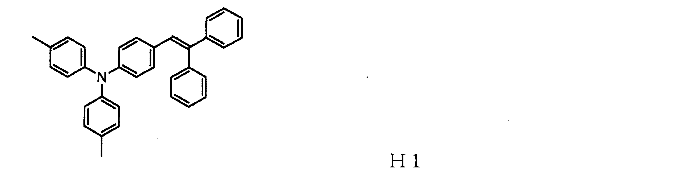

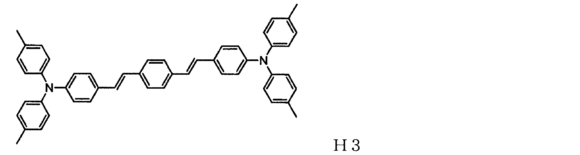
電子輸送材料としては、下記化合物E1、E2およびE3を用いた。
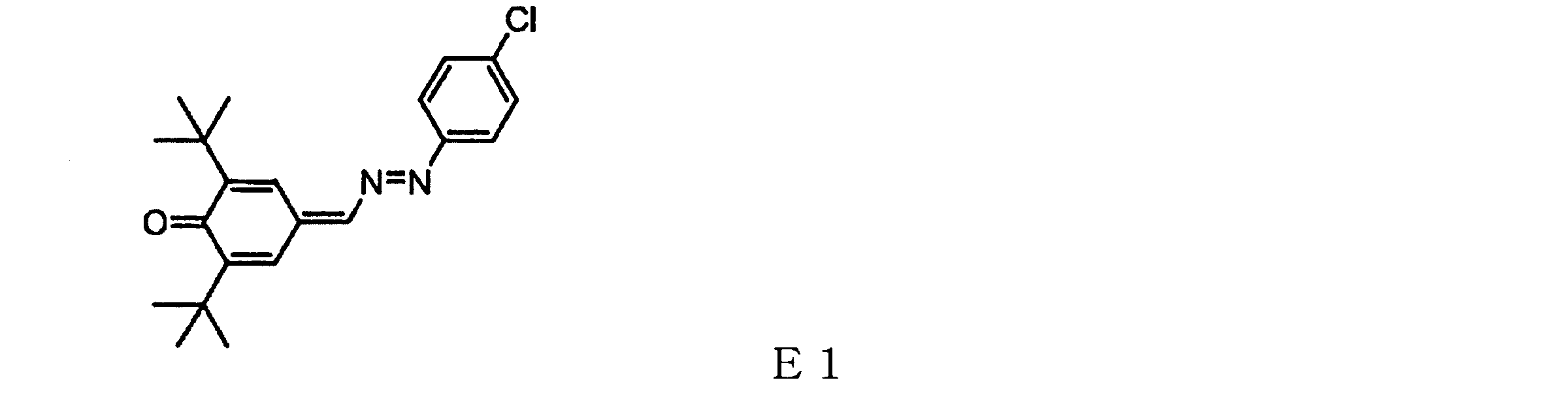


結着樹脂としては、それぞれ下記式で表される繰り返し単位を有するポリカーボネート系樹脂B1~B6を用いた。
B1:ポリカーボネート系樹脂(水蒸気透過率:9.12g/m2・day)

(1)
B2:ポリカーボネート系樹脂(水蒸気透過率:6.08g/m2・day)


B4:ポリカーボネート系樹脂(水蒸気透過率:2.08g/m2・day)


(2)
B6:ポリカーボネート系樹脂(水蒸気透過率:1.96g/m2・day)

(2)
B7:汎用ポリスチレン樹脂 東洋エンジニアリング社製GPPS(水蒸気透過率:30.0g/m2・day)
B8:汎用高分子ポリエステル樹脂 東洋紡社製バイロン290(水蒸気透過率:7.5g/m2・day)
B9:下記繰り返し単位を有する高分子ポリエステル樹脂(水蒸気透過率:7.5g/m2・day)

(3)
B10:汎用ポリアリレート樹脂 ユニチカ社製Uポリマー(水蒸気透過率12.1g/m2・day)
酸化防止剤としては、ヒンダードフェノール系酸化防止剤ジブチルヒドロキシトルエン(BHT)を用いた。
潤滑剤としては、信越化学製ジメチルシリコンオイルKF-54を用いた。
溶剤としては、テトラヒドロフランを用いた。
《単層型感光体用塗布液》
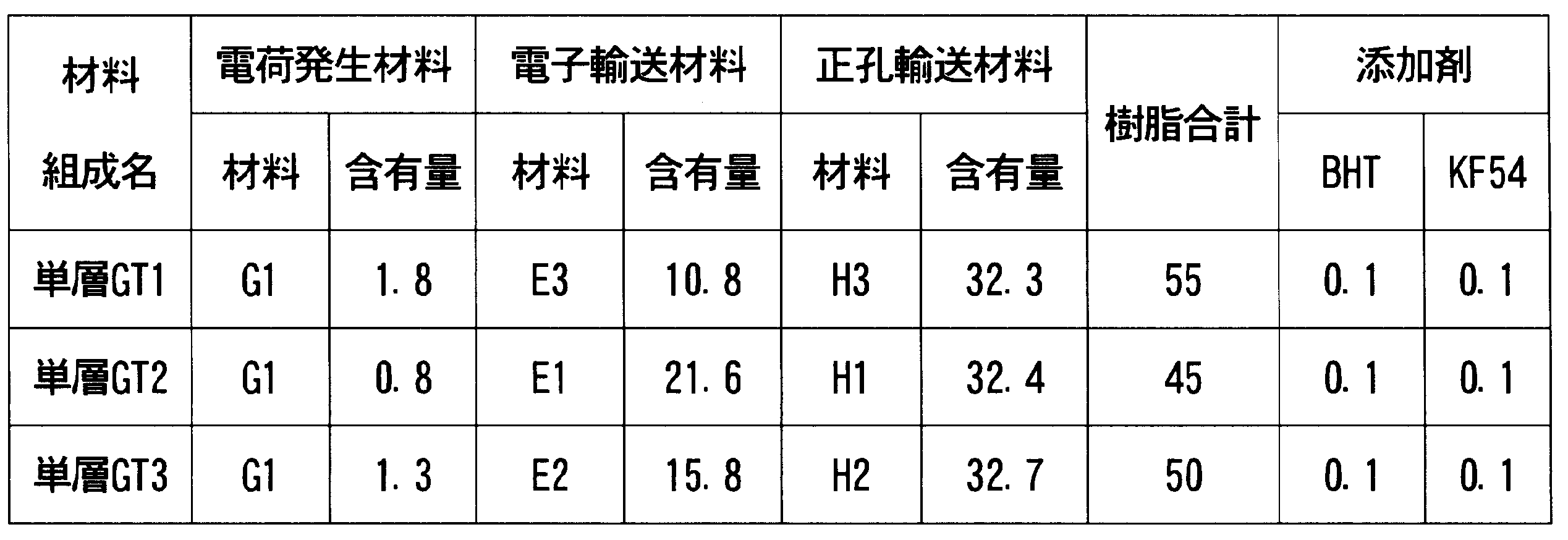
上記正孔輸送材料、電子輸送材料、結着樹脂および添加材料を所定の混合比で溶剤とともに容器に加え、溶解させた。次に、所定の質量比になるよう秤量した上記電荷発生材料を加え、ダイノーミル(シンマルエンタープライズ社のMULTILAB)で分散して、単層型感光体用塗布液を作製した。
結着樹脂以外の材料組成比を下記の表1に示す。表中の含有量は質量%を示す。
「電荷輸送層用塗布液」
上記正孔輸送材料、結着樹脂および添加材料を所定の混合比で溶剤とともに容器に加え、溶解させて、積層型感光体用の電荷輸送層用塗布液を作製した。
結着樹脂以外の材料組成比を下記の表2に示す。表中の含有量は質量%を示す。また、結着樹脂としては、上記B5の樹脂を用いた。
上記正孔輸送材料、電子輸送材料、結着樹脂および添加材料を所定の混合比で溶剤とともに容器に加え、溶解させた。次に、所定の重量比になるよう秤量した上記電荷発生材料を加え、ダイノーミル(シンマルエンタープライズ社のMULTILAB)で分散して、積層型感光体用の電荷発生層用塗布液を作製した。
結着樹脂以外の材料組成比を下記の表3に示す。表中の含有量は質量%を示す。

《単層型感光体》
上記表1に示す材料組成GT1の単層型感光体の塗布液を、結着樹脂を下記の表4、5に示すように変更して、上記導電性支持体上に浸漬塗工し、110℃にて60分間熱風乾燥することにより、膜厚20~35μmの単層型感光層を形成し、単層型感光体を作製した。実施例1~10および比較例1~9は20μm、実施例11~15および比較例10、11は27μm、実施例16~23および比較例12~15は35μmの膜厚とした。
また、上記表1に示す材料組成GT2およびGT3の単層型感光体の塗布液を、結着樹脂を下記の表5の実施例24、25に示すように変更して、上記導電性基体上に浸漬塗工し、110℃にて60分間熱風乾燥することにより、膜厚20μmおよび35μmの単層型感光層を形成し、単層型感光体を作製した。
上記表2に示す材料組成CT1の電荷輸送層塗布液を上記導電性支持体上に浸漬塗工し、110℃にて60分間熱風乾燥することにより、膜厚7μm、10μmおよび20μmの3種類の電荷輸送層を製膜した。次に、上記表3に示す材料組成G1の電荷発生層用塗布液を、結着樹脂を下記の表6、7に示すように変更して浸漬塗工し、110℃60分間の熱風乾燥を行って、膜厚13μm、17μm、15μmの3種類の電荷発生層を製膜して、全層膜厚がそれぞれ20μm、27μmおよび35μmの積層型感光体を作製した。
実施例26~35および比較例16~24は20μm、実施例36~40および比較例25、26は27μm、実施例41~48および比較例27~30は35μmの膜厚とした。
φ30mm×長さ244.5mm形状の感光体については、ブラザー工業(株)製の市販の50枚機のモノクロ高速レーザープリンタ(HL-6400DW)で、32℃湿度80%RH環境下にて10秒間欠で印字面積率4%の画像を1日5000枚で60000枚まで間欠印字を行い、翌日の朝一番の白紙画像の微小な黒点の発生状況(トナー紙粉の固着状況)を確認した。
φ30mm×長さ254.4mm形状の感光体については、ブラザー工業(株)製の市販の22枚機のタンデムカラーLEDプリンタ(HL-3170CDW)で、32℃湿度80%RH環境下にて、10秒間欠で印字面積率4%のカラー画像を1日3000枚で15000枚まで間欠印字を行い、翌日の朝一番の白紙画像の色ポチの発生状況(トナー紙粉の固着状況)を確認した。
《樹脂の水蒸気透過率評価》
JIS 7129:2008により、低湿度チャンバと高湿度チャンバとを試験片で区切り、1日放置後の透過した水蒸気絶対量をガスクロマトグラフィーにて検出した。
白紙部の微小な黒点または色ポチ(径が約0.5mm以下のもの)について、感光体周期で発生する個数を測定した。以下のように、3段階評価した。
○:5個以下、△:6~20個、×:21個以上
感光体表面上のトナーおよび紙粉の混合物の固着物個数を測定して、3段階評価した。
○:5個以下、△:6~20個、×:21個以上
これらの結果を、下記の表4~7中に併せて示す。
実施例1および実施例53~57の感光体については、さらに、1日の印字開始時に、べた白3枚および図5に示す画像3枚を印字し、以下のようなゴースト・かぶり評価を行った。図5の画像は、600dpi画像で、上部べた白画像中に▲のソリッド画像(塗りつぶされた三角形)を横方向に並べ、その下部に1ドット2スペースの点画画像:ハーフトーン(H/T)画像を配したゴースト評価画像である。この場合のゴースト画像とは、H/T画像上に△の形で周辺部より濃度が濃い部分が生ずることをいう。
ゴーストについては、この濃さの違いを、以下の基準に基づき目視で3段階評価した。
○:判別不可、△:僅かに判別可能、×:明確に判別可能
また、かぶりについては、べた白のかぶりレベルを以下の基準に基づき目視で3段階評価した。
○:かぶり観察不能、△:僅かに観察可能、×:明確に観察可能
この結果を、下記の表8中に併せて示す。




2 下引き層
3 単層型感光層
4 電荷輸送層
5 電荷発生層
7 電子写真用感光体
21 帯電器
22 高圧電源
23 像露光部材
241 現像ローラ
24 現像器
251 給紙ローラ
252 給紙ガイド
25 給紙部材
26 転写帯電器
27 紙紛回収部
300 感光層
60 電子写真装置
Claims (16)
- 導電性支持体と、
電荷発生材料、正孔輸送材料、電子輸送材料および結着樹脂を含み、前記導電性支持体上に設けられた単層型感光層と、を備える正帯電型電子写真用感光体であって、
前記結着樹脂がポリカーボネート系樹脂を含むとともに、前記結着樹脂の水蒸気透過率が、5~13g/m2・dayの範囲であることを特徴とする電子写真用感光体。 - 導電性支持体と、
少なくとも正孔輸送材料および結着樹脂を含み、前記導電性支持体上に設けられた電荷輸送層と、
少なくとも電荷発生材料、正孔輸送材料、電子輸送材料および結着樹脂を含み、前記電荷輸送層上に設けられた電荷発生層と、を備える正帯電型電子写真用感光体であって、
前記電荷発生層の結着樹脂がポリカーボネート系樹脂を含むとともに、前記電荷発生層の結着樹脂の水蒸気透過率が、5~13g/m2・dayの範囲であることを特徴とする電子写真用感光体。 - 前記水蒸気透過率が5~13g/m2・dayの範囲である結着樹脂が、下記式(1)で表される繰り返し単位を有する樹脂を含む請求項1記載の電子写真用感光体。
(1)
- 前記水蒸気透過率が5~13g/m2・dayの範囲である結着樹脂が、下記式(1)で表される繰り返し単位を有する樹脂を含む請求項2記載の電子写真用感光体。
(1)
- 前記水蒸気透過率が5~13g/m2・dayの範囲である結着樹脂が、下記式(1)で表される繰り返し単位を有する樹脂、および、下記式(2)で表される繰り返し単位を有する樹脂を含む請求項1記載の電子写真用感光体。
(1)
(2)
- 前記水蒸気透過率が5~13g/m2・dayの範囲である結着樹脂が、下記式(1)で表される繰り返し単位を有する樹脂、および、下記式(2)で表される繰り返し単位を有する樹脂を含む請求項2記載の電子写真用感光体。
(1)
(2)
- 前記水蒸気透過率が5~13g/m2・dayの範囲である結着樹脂が、下記式(2)で表される繰り返し単位を有する樹脂、および、下記式(3)で表される繰り返し単位を有する樹脂を含む請求項1記載の電子写真用感光体。
(2)
(3)
- 前記水蒸気透過率が5~13g/m2・dayの範囲である結着樹脂が、下記式(2)で表される繰り返し単位を有する樹脂、および、下記式(3)で表される繰り返し単位を有する樹脂を含む請求項2記載の電子写真用感光体。
(2)
(3)
- 前記電荷発生材料が少なくともチタニルフタロシアニンを含む請求項1記載の電子写真用感光体。
- 前記電荷発生材料が少なくともチタニルフタロシアニンを含む請求項2記載の電子写真用感光体。
- 請求項1記載の電子写真用感光体を製造する方法であって、前記水蒸気透過率が5~13g/m2・dayの範囲である結着樹脂を含む層を、浸漬塗工法を用いて製膜することを特徴とする電子写真用感光体の製造方法。
- 請求項2記載の電子写真用感光体を製造する方法であって、前記水蒸気透過率が5~13g/m2・dayの範囲である結着樹脂を含む層を、浸漬塗工法を用いて製膜することを特徴とする電子写真用感光体の製造方法。
- 請求項1記載の電子写真用感光体を搭載してなることを特徴とする電子写真装置。
- 請求項2記載の電子写真用感光体を搭載してなることを特徴とする電子写真装置。
- 重合トナーを用いた非磁性一成分接触現像方式のクリーナーレスプロセスを備える請求項13記載の電子写真装置。
- 重合トナーを用いた非磁性一成分接触現像方式のクリーナーレスプロセスを備える請求項14記載の電子写真装置。
Priority Applications (6)
| Application Number | Priority Date | Filing Date | Title |
|---|---|---|---|
| CN201780014372.1A CN109074007B (zh) | 2017-02-24 | 2017-02-24 | 电子照相用感光体、其制造方法及电子照相装置 |
| PCT/JP2017/007253 WO2018154739A1 (ja) | 2017-02-24 | 2017-02-24 | 電子写真用感光体、その製造方法およびそれを用いた電子写真装置 |
| DE112017000680.5T DE112017000680T5 (de) | 2017-02-24 | 2017-02-24 | Elektrofotografischer Fotoleiter, Herstellungsverfahren dafür und elektrofotografische Vorrichtung, die diesen verwendet |
| JP2018546572A JPWO2018154739A1 (ja) | 2017-02-24 | 2017-02-24 | 電子写真用感光体、その製造方法およびそれを用いた電子写真装置 |
| TW107100195A TWI665233B (zh) | 2017-02-24 | 2018-01-03 | 電子照相用感光體、其製造方法及使用其之電子照相裝置 |
| US16/117,144 US10429752B2 (en) | 2017-02-24 | 2018-08-30 | Electrophotographic photoconductor, manufacturing method thereof, and electrophotographic apparatus using the same |
Applications Claiming Priority (1)
| Application Number | Priority Date | Filing Date | Title |
|---|---|---|---|
| PCT/JP2017/007253 WO2018154739A1 (ja) | 2017-02-24 | 2017-02-24 | 電子写真用感光体、その製造方法およびそれを用いた電子写真装置 |
Related Child Applications (1)
| Application Number | Title | Priority Date | Filing Date |
|---|---|---|---|
| US16/117,144 Continuation US10429752B2 (en) | 2017-02-24 | 2018-08-30 | Electrophotographic photoconductor, manufacturing method thereof, and electrophotographic apparatus using the same |
Publications (1)
| Publication Number | Publication Date |
|---|---|
| WO2018154739A1 true WO2018154739A1 (ja) | 2018-08-30 |
Family
ID=63253572
Family Applications (1)
| Application Number | Title | Priority Date | Filing Date |
|---|---|---|---|
| PCT/JP2017/007253 Ceased WO2018154739A1 (ja) | 2017-02-24 | 2017-02-24 | 電子写真用感光体、その製造方法およびそれを用いた電子写真装置 |
Country Status (6)
| Country | Link |
|---|---|
| US (1) | US10429752B2 (ja) |
| JP (1) | JPWO2018154739A1 (ja) |
| CN (1) | CN109074007B (ja) |
| DE (1) | DE112017000680T5 (ja) |
| TW (1) | TWI665233B (ja) |
| WO (1) | WO2018154739A1 (ja) |
Cited By (1)
| Publication number | Priority date | Publication date | Assignee | Title |
|---|---|---|---|---|
| JP2020042178A (ja) * | 2018-09-11 | 2020-03-19 | 富士ゼロックス株式会社 | 電子写真感光体、プロセスカートリッジ、及び、画像形成装置 |
Families Citing this family (1)
| Publication number | Priority date | Publication date | Assignee | Title |
|---|---|---|---|---|
| US12317632B2 (en) * | 2021-05-12 | 2025-05-27 | Fujifilm Business Innovation Corp. | Coating device, coating method, and method for manufacturing photoconductor for suppressing occurrence of bubble defects in coated film |
Citations (4)
| Publication number | Priority date | Publication date | Assignee | Title |
|---|---|---|---|---|
| JP2001142234A (ja) * | 1999-11-12 | 2001-05-25 | Konica Corp | 電子写真感光体とその製造方法 |
| JP2007206130A (ja) * | 2006-01-31 | 2007-08-16 | Kyocera Mita Corp | 電子写真感光体及び画像形成装置 |
| JP2014092594A (ja) * | 2012-10-31 | 2014-05-19 | Kyocera Document Solutions Inc | 電子写真感光体及び画像形成装置 |
| JP2014109683A (ja) * | 2012-11-30 | 2014-06-12 | Kyocera Document Solutions Inc | 電子写真感光体及び画像形成装置 |
Family Cites Families (23)
| Publication number | Priority date | Publication date | Assignee | Title |
|---|---|---|---|---|
| JPS63221355A (ja) | 1986-03-18 | 1988-09-14 | Canon Inc | 電子写真感光体 |
| JPS6352146A (ja) | 1986-08-22 | 1988-03-05 | Konica Corp | 正帯電用電子写真感光体 |
| JPS6432264A (en) | 1987-07-29 | 1989-02-02 | Mita Industrial Co Ltd | Positively chargeable organic laminated photosensitive body |
| JP2732697B2 (ja) | 1990-03-07 | 1998-03-30 | 三田工業株式会社 | 両帯電可能な電子写真用有機感光体 |
| JP2507190B2 (ja) | 1991-01-14 | 1996-06-12 | 松下電器産業株式会社 | 電子写真感光体 |
| JP2961561B2 (ja) | 1991-01-17 | 1999-10-12 | コニカ株式会社 | 電子写真感光体 |
| JP2662115B2 (ja) | 1991-08-19 | 1997-10-08 | 三田工業株式会社 | 電子写真感光体 |
| JPH07160017A (ja) | 1993-12-02 | 1995-06-23 | Ricoh Co Ltd | 電子写真感光体 |
| JP3869734B2 (ja) | 2002-02-04 | 2007-01-17 | 大日本印刷株式会社 | 電荷発生層ならびに電荷注入・輸送層、およびこれを用いた有機感光体 |
| JP2004240056A (ja) | 2003-02-04 | 2004-08-26 | Fuji Denki Gazo Device Kk | 正帯電単層型電子写真用感光体 |
| JP3980547B2 (ja) * | 2003-11-07 | 2007-09-26 | 京セラミタ株式会社 | ポリカーボネート樹脂、電子写真感光体および画像形成装置 |
| JP2007121733A (ja) | 2005-10-28 | 2007-05-17 | Kyocera Mita Corp | 電子写真感光体 |
| JP2007163523A (ja) | 2005-12-09 | 2007-06-28 | Kyocera Mita Corp | 電子写真感光体及び画像形成装置 |
| JP2007256768A (ja) | 2006-03-24 | 2007-10-04 | Kyocera Mita Corp | 電子写真感光体及び画像形成装置 |
| US20120003574A1 (en) | 2008-02-22 | 2012-01-05 | Fuji Electric Systems Co., Ltd. | Electrophotography photoreceptor, method of manufacturing the same, and electrophotography device using the same |
| JP5233419B2 (ja) | 2008-05-29 | 2013-07-10 | 富士電機株式会社 | 電子写真用感光体およびその製造方法 |
| CN101713933B (zh) * | 2008-10-08 | 2013-01-02 | 京瓷办公信息系统株式会社 | 带正电单层型电子照相感光体和图像形成装置 |
| JP5564831B2 (ja) | 2009-05-26 | 2014-08-06 | 株式会社リコー | 電子写真感光体、並びにそれを用いた画像形成装置及びプロセスカートリッジ |
| WO2013021430A1 (ja) * | 2011-08-05 | 2013-02-14 | 富士電機株式会社 | 電子写真用感光体、その製造方法およびそれを用いた電子写真装置 |
| US9548275B2 (en) * | 2013-05-23 | 2017-01-17 | Globalfoundries Inc. | Detecting sudden changes in acceleration in semiconductor device or semiconductor packaging containing semiconductor device |
| US9316933B2 (en) * | 2013-07-09 | 2016-04-19 | Sharp Kabushiki Kaisha | Electrophotographic photoreceptor and image forming apparatus including the same |
| WO2015008322A1 (ja) | 2013-07-16 | 2015-01-22 | 富士電機株式会社 | 電子写真用感光体、その製造方法および電子写真装置 |
| JP6354668B2 (ja) * | 2015-06-08 | 2018-07-11 | 京セラドキュメントソリューションズ株式会社 | 正帯電単層型電子写真感光体、プロセスカートリッジ、及び画像形成装置 |
-
2017
- 2017-02-24 JP JP2018546572A patent/JPWO2018154739A1/ja active Pending
- 2017-02-24 WO PCT/JP2017/007253 patent/WO2018154739A1/ja not_active Ceased
- 2017-02-24 DE DE112017000680.5T patent/DE112017000680T5/de not_active Withdrawn
- 2017-02-24 CN CN201780014372.1A patent/CN109074007B/zh active Active
-
2018
- 2018-01-03 TW TW107100195A patent/TWI665233B/zh not_active IP Right Cessation
- 2018-08-30 US US16/117,144 patent/US10429752B2/en active Active
Patent Citations (4)
| Publication number | Priority date | Publication date | Assignee | Title |
|---|---|---|---|---|
| JP2001142234A (ja) * | 1999-11-12 | 2001-05-25 | Konica Corp | 電子写真感光体とその製造方法 |
| JP2007206130A (ja) * | 2006-01-31 | 2007-08-16 | Kyocera Mita Corp | 電子写真感光体及び画像形成装置 |
| JP2014092594A (ja) * | 2012-10-31 | 2014-05-19 | Kyocera Document Solutions Inc | 電子写真感光体及び画像形成装置 |
| JP2014109683A (ja) * | 2012-11-30 | 2014-06-12 | Kyocera Document Solutions Inc | 電子写真感光体及び画像形成装置 |
Cited By (2)
| Publication number | Priority date | Publication date | Assignee | Title |
|---|---|---|---|---|
| JP2020042178A (ja) * | 2018-09-11 | 2020-03-19 | 富士ゼロックス株式会社 | 電子写真感光体、プロセスカートリッジ、及び、画像形成装置 |
| JP7180222B2 (ja) | 2018-09-11 | 2022-11-30 | 富士フイルムビジネスイノベーション株式会社 | 電子写真感光体、プロセスカートリッジ、及び、画像形成装置 |
Also Published As
| Publication number | Publication date |
|---|---|
| US10429752B2 (en) | 2019-10-01 |
| DE112017000680T5 (de) | 2018-10-31 |
| US20180373172A1 (en) | 2018-12-27 |
| CN109074007B (zh) | 2022-01-25 |
| TW201831556A (zh) | 2018-09-01 |
| JPWO2018154739A1 (ja) | 2019-03-07 |
| TWI665233B (zh) | 2019-07-11 |
| CN109074007A (zh) | 2018-12-21 |
Similar Documents
| Publication | Publication Date | Title |
|---|---|---|
| JP4838208B2 (ja) | 電子写真感光体、及びその製造方法、画像形成装置、並びに、プロセスカートリッジ | |
| JP5782125B2 (ja) | 電子写真用感光体、その製造方法およびそれを用いた電子写真装置 | |
| CN110392865A (zh) | 电子摄影用感光体、其制造方法以及电子摄影装置 | |
| JP6583563B2 (ja) | 電子写真用感光体、その製造方法およびそれを用いた電子写真装置 | |
| JP2021128347A (ja) | 電子写真用感光体、その製造方法および電子写真装置 | |
| US7851118B2 (en) | Image forming method, image forming apparatus and organic photoreceptor | |
| WO2018154739A1 (ja) | 電子写真用感光体、その製造方法およびそれを用いた電子写真装置 | |
| JP6020679B2 (ja) | 電子写真用感光体、その製造方法およびそれを用いた電子写真装置 | |
| WO2015008322A1 (ja) | 電子写真用感光体、その製造方法および電子写真装置 | |
| JP3952833B2 (ja) | 有機感光体、画像形成方法、画像形成装置及びプロセスカートリッジ | |
| CN112305877B (zh) | 电子摄影用感光体、其制造方法以及搭载其的电子摄影装置 | |
| WO2005073814A1 (ja) | 電子写真感光体及び電子写真装置 | |
| JPH039380A (ja) | 電子写真用帯電部材 | |
| US20200110335A1 (en) | Electrophotographic photoreceptor and electrophotographic device equipped with the same | |
| JP2007011253A (ja) | 有機感光体、画像形成方法、画像形成装置及びプロセスカートリッジ | |
| JP2006234924A (ja) | 有機感光体、画像形成方法及び画像形成装置 | |
| JP2007114649A (ja) | 有機感光体、画像形成方法、画像形成装置及びプロセスカートリッジ | |
| JPH0310266A (ja) | 電子写真用帯電部材 | |
| JP2007010958A (ja) | 有機感光体、画像形成方法、画像形成装置及びプロセスカートリッジ | |
| JP2006234925A (ja) | 有機感光体、画像形成方法及び画像形成装置 | |
| JP2007010959A (ja) | 有機感光体、画像形成方法、画像形成装置及びプロセスカートリッジ | |
| JPH04346358A (ja) | 電子写真感光体 | |
| JP2007010961A (ja) | 有機感光体、画像形成方法、画像形成装置及びプロセスカートリッジ | |
| WO2005064416A1 (ja) | 電子写真感光体及び電子写真装置 | |
| JPH04346357A (ja) | 電子写真感光体 |
Legal Events
| Date | Code | Title | Description |
|---|---|---|---|
| ENP | Entry into the national phase |
Ref document number: 2018546572 Country of ref document: JP Kind code of ref document: A |
|
| WWE | Wipo information: entry into national phase |
Ref document number: 112017000680 Country of ref document: DE |
|
| 121 | Ep: the epo has been informed by wipo that ep was designated in this application |
Ref document number: 17897555 Country of ref document: EP Kind code of ref document: A1 |
|
| 122 | Ep: pct application non-entry in european phase |
Ref document number: 17897555 Country of ref document: EP Kind code of ref document: A1 |