WO2018135220A1 - 電子装置 - Google Patents
電子装置 Download PDFInfo
- Publication number
- WO2018135220A1 WO2018135220A1 PCT/JP2017/045673 JP2017045673W WO2018135220A1 WO 2018135220 A1 WO2018135220 A1 WO 2018135220A1 JP 2017045673 W JP2017045673 W JP 2017045673W WO 2018135220 A1 WO2018135220 A1 WO 2018135220A1
- Authority
- WO
- WIPO (PCT)
- Prior art keywords
- electronic device
- resistor
- connection terminal
- external connection
- mos transistor
- Prior art date
- Legal status (The legal status is an assumption and is not a legal conclusion. Google has not performed a legal analysis and makes no representation as to the accuracy of the status listed.)
- Ceased
Links
Images






Classifications
-
- H—ELECTRICITY
- H10—SEMICONDUCTOR DEVICES; ELECTRIC SOLID-STATE DEVICES NOT OTHERWISE PROVIDED FOR
- H10D—INORGANIC ELECTRIC SEMICONDUCTOR DEVICES
- H10D89/00—Aspects of integrated devices not covered by groups H10D84/00 - H10D88/00
- H10D89/60—Integrated devices comprising arrangements for electrical or thermal protection, e.g. protection circuits against electrostatic discharge [ESD]
- H10D89/601—Integrated devices comprising arrangements for electrical or thermal protection, e.g. protection circuits against electrostatic discharge [ESD] for devices having insulated gate electrodes, e.g. for IGFETs or IGBTs
- H10D89/911—Integrated devices comprising arrangements for electrical or thermal protection, e.g. protection circuits against electrostatic discharge [ESD] for devices having insulated gate electrodes, e.g. for IGFETs or IGBTs using passive elements as protective elements
-
- H—ELECTRICITY
- H10—SEMICONDUCTOR DEVICES; ELECTRIC SOLID-STATE DEVICES NOT OTHERWISE PROVIDED FOR
- H10D—INORGANIC ELECTRIC SEMICONDUCTOR DEVICES
- H10D89/00—Aspects of integrated devices not covered by groups H10D84/00 - H10D88/00
- H10D89/60—Integrated devices comprising arrangements for electrical or thermal protection, e.g. protection circuits against electrostatic discharge [ESD]
- H10D89/601—Integrated devices comprising arrangements for electrical or thermal protection, e.g. protection circuits against electrostatic discharge [ESD] for devices having insulated gate electrodes, e.g. for IGFETs or IGBTs
- H10D89/811—Integrated devices comprising arrangements for electrical or thermal protection, e.g. protection circuits against electrostatic discharge [ESD] for devices having insulated gate electrodes, e.g. for IGFETs or IGBTs using FETs as protective elements
Definitions
- the present invention relates to an electronic device having a surge protection circuit configured by connecting a protective resistor and a plurality of semiconductor elements in parallel, and more particularly to an electronic device having a surge protection circuit optimal for a fine integrated circuit.
- Patent Document 1 discloses that current concentration is reduced by arranging protective resistors in all of a plurality of MOS transistors connected to an external connection terminal.
- a protective resistor is disposed in the vicinity of the MOS transistor, and the external connection terminal and the protective resistor are connected using a Yagi antenna-like wiring from the external connection terminal.
- an external connection terminal of an integrated circuit is directly connected to an external connection terminal of the electronic device.
- the external connection terminal of the integrated circuit needs to have surge resistance required for the external connection terminal of the electronic device.
- the surge resistance of the external connection terminal of the electronic device is higher than the surge resistance required for the integrated circuit.
- an electronic device for an automobile requires an energy tolerance of 100 times or more compared to the surge resistance required for an integrated circuit.
- the magnitude of the current flowing through the integrated circuit when a surge is applied and the time for which the current is applied are 10 times or more the surge resistance required for conventional integrated circuits.
- the present invention has been made in view of the above circumstances, and an object thereof is to increase the surge resistance of an external connection terminal of an integrated circuit without increasing the size, and the external connection terminal of the integrated circuit can be used as an external connection terminal such as an electronic device. To provide an electronic device that can be directly connected.
- the present invention connects an external connection terminal to a protective resistor, connects the protective resistor to a semiconductor device in which a plurality of semiconductor elements are connected in parallel, and forms a slit or a continuous hole in the protective resistor. Deploy.
- the protection circuit of the electronic device of this embodiment includes a semiconductor device.
- the semiconductor device includes an external connection terminal 1 for connecting to an external signal, a wiring layer 2 for connecting the external connection terminal 1 and the protective resistor 3, and a protective resistor for protecting the internal circuit from surges and noises input from the external connection terminal 1.
- Transistors 19 to 26 are provided.
- the MOS transistors 19 to 26 are a plurality of semiconductor elements connected in parallel. This semiconductor device is used to control sensors or actuators inside or outside the semiconductor device.
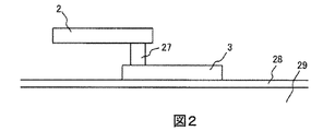
- the protective resistor 3 is connected to the wiring layer 2 via the contact 27.
- the protective resistor 3 is provided on the oxide film 28 provided on the silicon substrate 29.
- the protective resistor 3 is insulated from the silicon substrate 29 by an oxide film 28 which is an insulating film. In this way, insulation was ensured against positive and negative potential surges applied to the external connection terminal 1.
- a polysilicon film, a metal film, a metal silicide film, or the like can be used.
- the contact 27 is not limited, and may be a through hole.
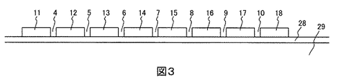
- the protective resistor 3 is divided by slits 4 to 10 to constitute current distribution resistors 11 to 18.
- the MOS transistors 21 to 26 have the same configuration as the MOS transistors 19 and 20.
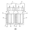
- a source 37 and a drain 39 are configured by a gate electrode 38 disposed in the diffusion layer 36.
- the source 37 is connected to the ground.
- the drain 39 is connected to the current distribution resistor 11 through the wiring layer 34 and the contacts 30 and 31.
- a source 40 and a drain 42 are configured by a gate electrode 41 disposed in the diffusion layer 43.
- the source 40 is connected to the ground.
- the drain 42 is connected to the current distribution resistor 12 through the wiring layer 35 and the contacts 32 and 33.
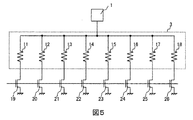
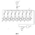
- the circuit diagram of the protection circuit of this embodiment is represented as shown in FIG. That is, the current (voltage) input from the external connection terminal 1 is connected to the current distribution resistors 11 to 18 configured by dividing the protective resistor 3.
- the current distribution resistors 11, 12, 13, 14, 15, 16, 17, 18 are connected to the MOS transistors 19, 20, 21, 22, 23, 24, 25, 26, respectively.
- the MOS transistors 19 to 26 drive the external connection terminal 1 by applying a signal to the gate electrode.
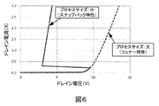
- the MOS transistors 19 to 26 exhibit a breakdown characteristic in which the drain current increases rapidly when the drain voltage is increased.
- a Zener characteristic is obtained as shown by a dotted line in FIG.
- the snapback characteristic is obtained as shown by the solid line in FIG.
- the snapback characteristics vary greatly between MOS transistors.
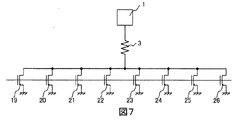
- FIG. 7 shows a protection circuit of an electronic device in the case of a conventional structure in which no slit is provided in the protection resistor 3.
- the rising speed of the surge voltage applied to the external connection terminal 1 is such that when the external connection terminal of the integrated circuit is directly connected to the external connection terminal of an electronic device or the like, reactance due to wiring, a capacitor added to the external connection terminal, or intentionally Slower due to added capacitors. That is, when the external connection terminal of the integrated circuit is directly connected to the external connection terminal of an electronic device or the like, it is necessary to consider that the surge voltage rise speed is slow and the withstand capability of the protection circuit is reduced.
- slits 4 to 10 are provided in the protection resistor 3 to form current distribution resistors 11 to 18.
- the external connection terminal 1, the protective resistor 3, and the MOS transistors 19 to 26 are connected in the shortest distance.
- the wiring layers 2, 34, and 35 connecting them can be short and the wiring width can be increased.
- the current capacity of the wiring layers 2, 34, and 35 can be increased, and wiring damage due to a surge voltage applied to the external connection terminal 1 can be reduced.
- the layout pitch of the slits 4 to 10 and the MOS transistors 19 to 26 can be easily matched. From this, it is possible to improve the connectivity between the current distribution resistors 11 to 18 and the MOS transistors 19 to 26, and to reduce the chip size and the current capacities of the wiring layers 34 and 35.
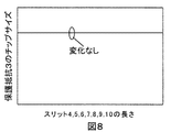
- FIG. 8 shows the relationship between the lengths of the slits 4 to 10 and the size of the protective resistor 3. Even if the slits 4 to 10 are lengthened, the chip size of the protective resistor 3 does not change.
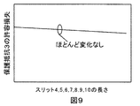
- FIG. 9 shows the relationship between the length of the slits 4 to 10 and the allowable loss of the protective resistor 3.
- the allowable loss of the protective resistor 3 is determined by the plane area of the protective resistor 3.
- the plane area of the protective resistor 3 is reduced by the slits 4 to 10.
- this amount is very small, the allowable loss of the protective resistor 3 hardly changes even if the slits 4 to 10 are lengthened.
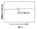
- FIG. 10 shows the relationship between the length of the slits 4 to 10 and the resistance value of the protective resistor 3.
- the resistance value of the protective resistor 3 is determined by the resistivity, width, and length of the protective resistor 3.
- the width of the protective resistor 3 is reduced by the slits 4 to 10. However, since this amount is very small, the resistance value of the protective resistor 3 hardly changes.
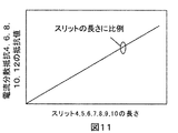
- FIG. 11 shows the relationship between the lengths of the slits 4 to 10 and the resistance values of the current distribution resistors 11 to 18.
- the resistance values of the current distribution resistors 11 to 18 increase proportionally. That is, by making the slits 4 to 10 long, the current distribution resistors 11 to 18 having high resistance values can be realized without changing the design values such as the size, allowable loss, and resistance value of the protective resistor 3. That is, the resistance values of the current distribution resistors 11 to 18 can be easily increased by making the slits 4 to 10 longer.
- the current flowing to the current distribution resistors 11 to 18 and the MOS transistors 19 to 26 can be limited.
- the connection wiring to the MOS transistors 19 to 26 can be prevented from being damaged.
- This effect is more preferable because the effect on the area of the protective resistor 3 can be maximized by disposing the slits 4 to 10 in the direction of current flow, but is not limited thereto. If the slits 4 to 10 are extended in an oblique direction, the slit hits the side end of the protective resistor 3, and the slit length is limited with respect to the energization direction. In other words, even when the slits 4 to 10 are stretched in an oblique direction, the effect is reduced but the effect is exhibited.
- the resistance value from the external connection terminal 1 to the ground through the current distribution resistor 11 and the MOS transistor 19 and the ground value from the external connection terminal 1 through the current distribution resistor 12 and the MOS transistor 20 are ground.
- the resistance value until the resistance is removed from the external connection terminal 1 to the ground through the current distribution resistor 15 and the MOS transistor 23, and the resistance value from the external connection terminal 1 to the ground via the current distribution resistance 16 and the MOS transistor 24 The resistance value until it is released, the current distribution resistor 17 from the external connection terminal 1, the MOS transistor And resistance to escape to the ground through a 25, Dekiru small Ku the variation in resistance to escape to the ground through a current spreading resistance 18, MOS transistor 26 from the external connection terminal 1.
- the resistance value from the external connection terminal 1 to the MOS transistors 19 to 26 is determined by the resistance value of the current distribution resistors 11 to 18, but when there is no slit, the MOS transistor 19 provided at the end is connected to the external connection.
- the path where the resistance value to the terminal 1 is the minimum and the path where the resistance value from the MOS transistor 22 disposed in the center to the external connection terminal 1 is the minimum are different, and the difference in this path results in variations in the resistance value. Therefore, in this embodiment, the variation in resistance value from the external connection terminal 1 to the ground via the current distribution resistor and the MOS transistor can be reduced as compared with the case where there is no slit. As a result, the current flowing through the protective resistor 3 can be made uniform, the current concentration of the current flowing through the protective resistor 3 can be reduced, the allowable loss of the protective resistor 3 can be increased, and the chip size can be reduced.
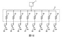
- the protection circuit of the electronic device of this embodiment is basically the same as that of the electronic device of the first embodiment, but MOS transistors 19 to 26 are diode-connected and MOS diodes 44 to 51 are arranged. Even in this case, the same effect as the electronic device of the first embodiment can be obtained.
- the external connection terminal 1 can be used as an input terminal.
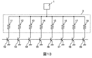
- the protection circuit of the electronic device of this embodiment is basically the same as that of the electronic device of the first embodiment, but the MOS transistors 19 to 26 are replaced with bipolar transistors 52 to 59. Even in this case, the same effect as the electronic device of the first embodiment can be obtained. Further, by arranging the bipolar transistors 52 to 59, variations in the transistors can be reduced, and a surge current can easily flow through each transistor, and the chip size can be reduced.
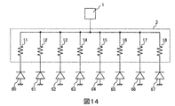
- the protection circuit of the electronic device of this embodiment is basically the same as that of the electronic device of the first embodiment, but the MOS transistors 19 to 26 are replaced with diodes 60 to 67. Even in this case, the same effect as the electronic device of the first embodiment can be obtained.
- the protection circuit of the electronic device of this example is basically the same as that of the first example, but the following changes were added.
- the slit disposed in the protective resistor 3 is shortened.
- the protective resistor 3 is provided with slits 69 to 75 shorter than the length of the protective resistor 3.
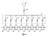
- the protective resistor 3 is configured with a resistor 68 and current distribution resistors 76 to 83.
- the external connection terminal 1 is connected to a resistor 68 constituted by a portion of the protective resistor 3 on the external connection terminal 1 side.
- the resistor 68 is connected to current spreading resistors 76 to 83 formed by dividing the protective resistor 3.
- Current distribution resistors 76-83 are connected to MOS transistor pairs 84-91.
- the external connection terminal 1 is driven by applying a signal to the gate electrodes of the MOS transistor pairs 84 to 91.
- the current of the protective resistor 3 that flows due to the surge voltage applied to the external connection terminal 1 tends to flow linearly from the external connection terminal 1 toward the MOS transistor pairs 84 to 91. This tendency is particularly great in the vicinity of the external connection terminal 1.
- the current due to the surge voltage tends to concentrate on the protective resistors 14 and 15.
- the wiring layer 2 becomes longer and the current capacity of the wiring layer 2 is reduced.
- the chip size increases.
- the slits 69 to 75 are made shorter than the protective resistor 3.
- the resistor 68 is further arranged in the protective resistor 3 by extending only to the middle of the protective resistor 3.
- the current flowing through the resistor 68 can be made uniform by the effect of the resistance increase due to reactance and heat generation, and the current to the current distribution resistors 76 to 83 can be made to flow evenly.
- a surge current can flow uniformly through the protective resistor 3.
- the middle was described as an example, it is not restricted to this. That is, it is possible to further dispose the resistor 68 by extending the stretching to the middle of the protective resistor 3.
- the resistance value of the current distribution resistors 76 to 83 is reduced, but in order to prevent damage to the wiring, it is determined by the maximum value of the surge voltage and the resistance value of the current distribution resistors 76 to 83. It is sufficient that the current capacity of the wiring is higher than the current value, and this condition can be satisfied sufficiently even if the slits 69 to 75 are shortened. This effect can be maximized when the slits 69 to 75 are arranged so as to extend from the connection end side with the MOS transistor pair 84 to 91.
- the slits 69 to 75 are slightly separated from the connection ends of the MOS transistor pairs 84 to 91, a resistance component is generated in the separated gap, and the substantial current distribution resistors 76 to 83 are affected by the resistance component. This is because the resistance value is lowered.
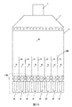
- MOS transistors 19 to 26 are replaced with MOS transistor pairs 84 to 91 as shown in FIGS.
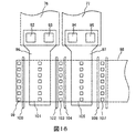
- MOS transistor pairs 84 and 85 Details of the MOS transistor pairs 84 and 85 will be described with reference to FIG.
- the MOS transistor pairs 86 to 91 have the same configuration as the MOS transistor pairs 84 and 85.
- the gate electrodes 100 and 102 are arranged in the diffusion layer 98 to constitute the sources 99 and 103 and the drain 101. Sources 99 and 103 are connected to ground. The drain 101 is connected to the current distribution resistor 76 through the wiring layer 96 and the contacts 92 and 93.
- the gate electrodes 104 and 106 are arranged in the diffusion layer 98 to constitute the sources 103 and 107 and the drain 105. Sources 103 and 107 are connected to ground. The drain 105 is connected to the current distribution resistor 77 through the wiring layer 97 and the contacts 94 and 95.
- the chip size can be reduced. Further, it is not necessary to provide a diffusion layer for each MOS transistor, and a plurality of MOS transistors can be arranged in one diffusion layer 98, so that the chip size can be reduced. Even if two MOS transistors are connected to each of the current distribution resistors 76 to 83 as in this embodiment, the maximum value of the surge current is determined by the maximum value of the surge voltage and the resistance value of the current distribution resistors 76 to 83. That is, even if a plurality of MOS transistors are connected to each of the current distribution resistors 76 to 83, the maximum value of the surge current hardly changes, so that damage to the wiring can be prevented.
- the tip of the slit 75 has a rounded shape as shown in FIG. In this way, by rounding the shape of the slit tip, a surge application current flowing for surge application flows smoothly, and heat generation at the tip portion can be suppressed.
- FIG. 19 shows the configuration of the protection circuit of the electronic device of the sixth embodiment. The description of the same structure as that of the fifth embodiment is omitted.
- the protection circuit of the electronic device of this embodiment is basically the same as that of the electronic device of the fifth embodiment, but the slits 69 and 75 on the side end side of the protection resistor 3 are shortened, and the central portion of the protection resistor 3 is The slits 71, 72, 73 were lengthened. In other words, the slit on the side end portion side is shorter than the slit on the center side. By doing so, the resistance value of the current distribution resistor on the side end portion side is reduced, and the surge current is more likely to flow to the side end portion of the protective resistor 3. When the external connection terminal 1 is located on the center side, the surge current tends to go straight, so that it tends to hardly flow to the side end portion side. According to this embodiment, since the resistance of the current distribution resistor far from the external connection terminal 1 (on the side end side) is reduced, the surge current can flow through the protective resistor 3 more evenly.
- FIG. 20 shows the configuration of the protection circuit of the electronic device of the seventh embodiment. The description of the same structure as in the fifth and sixth embodiments is omitted.
- the protection circuit of the electronic device of this embodiment is basically the same as that of the electronic device of the fifth embodiment, but the external connection terminal 1 is biased to the left. And the slit 75 of the side edge part of the protective resistance 3 was shortened, and the slits 69, 70, 71 near the external connection terminal 1 were lengthened. By doing so, the surge current is more likely to flow to the right side of the protective resistor 3. According to this embodiment, since the resistance of the current distribution resistor far from the external connection terminal 1 (on the right end side) is reduced, the surge current can flow through the protective resistor 3 more evenly. As a result, even if the external connection terminal 1 is biased to the left side, the surge current can flow through the protective resistor 3 more evenly. The same applies when the external terminal 1 is provided on the right side.
- the protection circuit of the electronic device of this embodiment is basically the same as that of the electronic device of the fifth embodiment, but the slits 69 to 75 are separated from the connection ends of the MOS transistor pairs 84 to 91. Even in such a case, the equivalent circuit of the protection circuit is the same as the circuit diagram of FIG. 18 shown in the fifth embodiment. That is, as in the fifth embodiment, the surge current that flows when a surge voltage is applied can flow through the protective resistor 3 more evenly, and the MOS transistor is activated by the surge current that flows when the surge voltage is applied. It is possible to prevent the connection wiring to the pairs 84 to 91 from being damaged.
- the protection circuit of the electronic device of this embodiment is basically the same as that of the electronic device of the fifth embodiment, but the number of slits is reduced by deleting the slits 69, 71, 73, and 75. Even in such a case, the current flowing to the MOS transistor pair 84 to 91 when the surge voltage is applied can be limited. As a result, it is possible to prevent the connection wiring to the MOS transistor pairs 84 to 91 from being damaged by the surge current that flows when the surge voltage is applied.
- the connection points of the MOS transistor pairs 84, 85, the connection points of the MOS transistor pairs 86, 87, the connection points of the MOS transistor pairs 88, 89, and the MOS transistor pairs 90, 91 By dividing the connection points, the current flowing to the MOS transistor pairs 84 to 91 when a surge voltage is applied can be limited.
- the protection resistor 3 is divided by the slits 70, 72, 74 to form a plurality of current distribution resistors, and the current distribution resistors are divided into MOS transistor pairs 84, 85 and MOS transistor pairs 86, 87.
- MOS transistor pair 88, 89 and MOS transistor pair 90, 91 are connected.
- the protection circuit of the electronic device of this embodiment is basically the same as that of the electronic device of the fifth embodiment, but the slits 69 to 75 are replaced with a series of holes 108 to 114. Even in such a case, the equivalent circuit of the protection circuit is the same as the circuit diagram of FIG. 18 shown in the fifth embodiment.
- the protection circuit of the electronic device of this embodiment is basically the same as that of the electronic device of the fifth embodiment, but the slits 69 to 75 are replaced with slits 115 to 130 arranged in an oblique direction. Even in such a case, the equivalent circuit of the protection circuit is the same as the circuit diagram of FIG. 18 shown in the fifth embodiment.
- the protection circuit of the electronic device of this embodiment is basically the same as that of the electronic device of the eleventh embodiment, but the slits 115 to 130 are replaced with angled slits 131 to 142. Even in such a case, the equivalent circuit of the protection circuit is the same as the circuit diagram of FIG. 18 shown in the fifth embodiment.
- the protection circuit of the electronic device of the present embodiment is basically the same as that of the electronic device of the fifth embodiment, but the wiring layer 143 is added, the capacitor 144 is disposed, and the internal circuit 145 such as an AD converter is connected. .
- a filter can be configured by the resistor 68 and the capacitor 144. By disposing the filter, surge voltage and high frequency noise entering from the external connection terminal 1 can be attenuated by this filter, and the internal circuit 145 can be stabilized.
- the chip size can be reduced by sharing the resistor 68 as a resistor used to achieve surge voltage protection and filter function.
- the protective resistor 3 is insulated from the silicon substrate 29 and the oxide film 28. As a result, insulation is secured against positive and negative potential surges applied to the external connection terminal 1. For this reason, the filter of this embodiment maintains an average value even when a voltage not lower than the power supply voltage or not higher than the ground voltage is input to the external connection terminal 1. That is, even if a high voltage such as a surge is applied to the external connection terminal 1, the filter of this embodiment can operate normally.
- the resistor 68 when a signal is taken into the internal circuit 145 from the wiring layer 143, the resistor 68 is inserted in series between the external connection terminal 1 and the internal circuit 145, and the current distribution resistors 76 to 83 and the MOS transistor pairs 84 to 91 are connected in series. The circuit enters parallel to ground. Therefore, the signal of the wiring layer 143, that is, the input signal to the internal circuit 145 is protected by a surge protection circuit including the resistor 68, current distribution resistors 76 to 83, and MOS transistor pairs 84 to 91.
- a surge protection circuit including the resistor 68, current distribution resistors 76 to 83, and MOS transistor pairs 84 to 91.
- the resistor 68 when the resistor 68 is inserted, a higher surge voltage attenuation effect can be obtained, and the internal circuit 145 weak against the surge voltage can be more strongly protected. As a result, damage and malfunction due to the surge voltage of the internal circuit 145 can be prevented, so that a
- FIG. 28 shows the configuration of the protection circuit of the electronic device according to the fourteenth embodiment.
- the protection circuit of the electronic device of this embodiment is basically the same as that of the electronic device of the first embodiment, but a wiring layer 145 is added. Since the equivalent circuit of this protection circuit is basically the same as the circuit diagram of FIG. 27 shown in the thirteenth embodiment, the surge current that flows when a surge voltage is applied is more equally protected as in the thirteenth embodiment.
- the resistor 3 can be made to flow, and the connection wiring to the MOS transistors 19 to 26 can be prevented from being damaged by the surge current that flows when a surge voltage is applied.
- the resistor 68 can be equivalently realized by adding the wiring layer 146, a filter can be configured by connecting the capacitor 144. By arranging the filter, surge voltage and high frequency noise entering from the external connection terminal 1 can be attenuated by this filter. As a result, damage and malfunction due to the surge voltage of the internal circuit 145 can be prevented, so that a more reliable electronic device can be provided.
- the slit has been described as an example of the pattern portion formed in the protective resistor, but the same effect can be obtained even if it is a groove.
- a continuous hole has been described as an example of the pattern portion formed in the protective resistor, but the same effect can be obtained even with a continuous recess.
- these pattern portions are not limited to the structure formed by etching or the like after the film formation, and naturally include other structures such as forming at the time of film formation by masking.
- SYMBOLS 1 External connection terminal, 2 ... Wiring layer, 3 ... Protection resistance, 4 ... Slit, 5 ... Slit, 6 ... Slit, 8 ... Slit, 9 ... Slit, 10 ... Slit, 11 ... Current dispersion resistance, DESCRIPTION OF SYMBOLS 12 ... Current distribution resistance, 13 ... Current distribution resistance, 14 ... Current distribution resistance, 15 ... Current distribution resistance, 16 ... Current distribution resistance, 17 ... Current distribution resistance, 18 ... Current distribution resistance, 19 ... MOS transistor, 20 ... MOS Transistor, 21 ... MOS transistor, 22 ... MOS transistor, 23 ... MOS transistor, 24 ... MOS transistor, 25 ... MOS transistor, 26 ...
- Continuous hole 110 a row of holes, 111, a row of holes, 112, a row of holes, 113, a row of holes, 114, a row of holes, 115, slits, 116, slits, 117... Slit, 118... Slit, 119... Slit, 120. Slit, 121. Slit, 122. Slit, 123. Slit, 124. Slit, 125. Slit, 126. Slit, 127. Slit, 130 ... Slit, 131 ... Slit, 132 ... Slit, 133 ... Slit, 134 ...
Landscapes
- Semiconductor Integrated Circuits (AREA)
- Metal-Oxide And Bipolar Metal-Oxide Semiconductor Integrated Circuits (AREA)
Abstract
従来の電子装置の保護回路ではサージ耐性が低く、集積回路の外部接続端子を電子装置などの外部接続端子に直接接続することが困難であった。 本実施例の電子装置の保護回路は外部信号を接続すると外部接続端子1、外部接続端子1と保護抵抗3を接続する配線層2と、外部接続端子1から入力されるサージやノイズから内部回路を保護する保護抵抗3と、保護抵抗3を分割するスリット4、5、6、7、8、9、10と、保護抵抗3をスリット4、5、6、7、8、9、10で分割することで構成される電流分散抵抗11、12、13、14、15、16、17、18と、電流分散抵抗11、12、13、14、15、16、17、18に接続されるMOSトランジスタ19、20、21、22、23、24、25、26から構成される。
Description
本発明は保護抵抗と複数の半導体素子を並列接続して構成されるサージ保護回路を有する電子装置に係り、特に、微細集積回路に最適なサージ保護回路を有する電子装置に関する。
保護抵抗と複数の半導体素子を並列接続して構成されるサージ保護回路を有する電子装置の例として、特許文献1に記載された技術がある。特許文献1には、外部接続端子に接続される複数のMOSトランジスタの全てに保護抵抗を配置することで電流集中を低減することが開示されている。また、保護抵抗をMOSトランジスタの近傍に配置し、外部接続端子からの八木アンテナ状の配線を用いて外部接続端子と保護抵抗を接続していた。
センサなどの小型の電子装置では、集積回路の外部接続端子を電子装置の外部接続端子に直接接続することが行われる。この場合、集積回路の外部接続端子には電子装置の外部接続端子に要求されるサージ耐性が必要になる。また、電子装置の外部接続端子のサージ耐性は集積回路に要求されるサージ耐性に比べて高い。特に、自動車用電子装置では、集積回路に要求されるサージ耐性に比べて100倍以上のエネルギー耐量を要求する。この結果、サージ印加時に集積回路に流れる電流の大きさおよび印加される時間は、従来の集積回路に要求されるサージ耐性の10倍以上になる。
このような大きなサージ耐性を得る場合、保護抵抗のサイズは大型化し、MOSトランジスタのサイズ及び個数も増加する。そして、保護抵抗およびMOSトランジスタのサイズが大きくなった場合、保護抵抗をMOSトランジスタの近傍に配置するレイアウトでは、レイアウト効率が悪くチップサイズが大きくなってしまう。また、サージ印加により発生する電流の電流集中によって破損する箇所については、MOSトランジスタだけではなく、配線も考慮する必要がある。配線の保護も考慮する場合、外部接続端子から八木アンテナ状の配線を用いて保護抵抗に接続したのでは配線長が長く、且つ、細くなるので配線の電流容量を増加させることが困難である。また、配線の電流容量を増加させようとすると、配線が太くなりチップサイズが増加してしまう。これらのことに対して、特許文献1は配慮が欠けていた。
本発明は上記事情に鑑みてなされたものであり、その目的は、集積回路の外部接続端子のサージ耐性を大型化することなく高め、集積回路の外部接続端子を電子装置などの外部接続端子に直接接続できる電子装置を提供することにある。
上記課題を解決するために、本発明は、外部接続端子を保護抵抗に接続し、前記保護抵抗を複数の半導体素子を並列接続した半導体デバイスに接続し、前記保護抵抗にスリットあるいは連続する穴を配置する。
本発明によれば、小型でサージ耐性の高い電子装置を提供することが可能となる。
以下、本発明の実施の形態について、図面を参照して説明する。なお、各実施例は、矛盾しない限り組み合わせ可能である。
[第1の実施例]
まず、本発明の第1の実施例である電子装置を図1~11により説明する。
まず、本発明の第1の実施例である電子装置を図1~11により説明する。
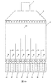
図1に示すように、本実施例の電子装置の保護回路は、半導体デバイスを備える。半導体デバイスは、外部信号と接続する外部接続端子1と、外部接続端子1と保護抵抗3を接続する配線層2と、外部接続端子1から入力されるサージやノイズから内部回路を保護する保護抵抗3と、保護抵抗3を分割するスリット4~10と、保護抵抗3をスリット4~10で分割することで構成される電流分散抵抗11~18と、電流分散抵抗11~18に接続されるMOSトランジスタ19~26を備える。MOSトランジスタ19~26は、並列接続された複数の半導体素子である。この半導体デバイスは、半導体装置の内部若しくは外部のセンサやアクチュエータを制御するのに用いられる。
図2に示す様に、保護抵抗3は、コンタクト27を介して配線層2と接続している。保護抵抗3は、シリコン基板29の上に設けられた酸化膜28上に設けられている。保護抵抗3は、絶縁膜である酸化膜28により、シリコン基板29と絶縁されている。こうすることで、外部接続端子1に印加される正電位および負電位のサージに対して絶縁性を確保した。保護抵抗3は、ポリシリコン膜、金属膜、金属シリサイド膜などを使用できる。また、コンタクト27には限定されず、スルーホールなどでもよい。
図3に示す様に、保護抵抗3は、スリット4~10で分割され、電流分散抵抗11~18を構成する。
図4を用いてMOSトランジスタ19、20の詳細を説明する。なお、MOSトランジスタ21~26もMOSトランジスタ19、20と同様な構成である。MOSトランジスタ19は、拡散層36に配置されたゲート電極38により、ソース37とドレイン39を構成する。ソース37は、グランドに接続される。ドレイン39は、配線層34、コンタクト30、31を介して電流分散抵抗11に接続される。MOSトランジスタ20は、拡散層43に配置されたゲート電極41により、ソース40とドレイン42を構成する。ソース40は、グランドに接続する。ドレイン42は、配線層35、コンタクト32、33を介して電流分散抵抗12に接続される。
図1、2、3、4に示す様に保護回路を構成することで、本実施例の保護回路の回路図は図5の様に表される。つまり、外部接続端子1から入力された電流(電圧)は、保護抵抗3を分割して構成した電流分散抵抗11~18に接続される。電流分散抵抗11、12、13、14、15、16、17、18は、各々MOSトランジスタ19、20、21、22、23、24、25、26に接続される。MOSトランジスタ19~26は、ゲート電極に信号を印加することで、外部接続端子1を駆動する。
次に、本実施例の第1の効果について説明する。
MOSトランジスタ19~26は、図6に示す様に、ドレイン電圧を増加させるとドレイン電流が急増する降伏特性を示す。ここで、MOSトランジスタ19~26のプロセスサイズが大きい場合は、図6の点線で示す様にツェナー特性になる。他方で、MOSトランジスタ19~26のプロセスサイズが小さい(微細プロセス)場合は、図6の実線に示す様に、スナップバック特性になる。ここで、スナップバック特性はMOSトランジスタ毎のバラツキが大きいという課題がある。
ここで、図7に、保護抵抗3にスリットを設けない従来構造の場合における電子装置の保護回路を示す。この従来構造における外部接続端子1に、サージ電圧が印加された場合を考える。外部接続端子1にサージが印加されると、MOSトランジスタ19~26のドレイン電圧は上昇し、最もスナップバックし易いMOSトランジスタが最初にスナップバックする。この結果、MOSトランジスタ19~26のドレイン電圧は低下するので、最初にスナップバックしたMOSトランジスタはスナップバックした状態になり、他のMOSトランジスタはスナップバックしなくなる。この結果、最初にスナップバックしたMOSトランジスタに電流が集中して流れ、最初にスナップバックしたMOSトランジスタの接続配線が損傷してしまう。
この現象は、外部接続端子1に印加されるサージ電圧の立ち上がり速度が遅い場合に顕著に表れる。これは、MOSトランジスタのドレイン電圧がスナップバックする電圧まで達したとしても、MOSトランジスタがスナップバックするまでに時間を要することに起因する。つまり、サージ電圧の立ち上がり速度が速く、MOSトランジスタが実際にスナップバックするまでの時間よりもサージ電圧の立ち上がり時間が短い場合には、あるMOSトランジスタのドレイン電圧がスナップバックする電圧まで達してから、他のMOSトランジスタがスナップバックするまでに上昇する。すなわち、あるMOSトランジスタのドレイン電圧がスナップバックするまでの遅延時間の間に、他のMOSトランジスタもスナップバックする。しかし、サージ電圧の立ち上がり速度が遅い場合には、どれか1つのMOSトランジスタが最初にスナップバックすると他のMOSトランジスタのドレイン電圧がスナップバックする電圧まで上昇しないので、最初にスナップバックしたMOSトランジスタに電流が集中する。
外部接続端子1に印加されるサージ電圧の立ち上がり速度は、集積回路の外部接続端子を電子装置などの外部接続端子に直接接続した場合、配線によるリアクタンス、外部接続端子に付加するコンデンサや意図的に付加したコンデンサなどにより遅くなる。つまり、集積回路の外部接続端子を、電子装置などの外部接続端子に直接接続する場合は、サージ電圧の立ち上がり速度が遅くなり、保護回路の耐量が小さくなることを考慮する必要がある。
次に、本実施例の保護回路の外部接続端子1にサージが印加された場合を考える。本実施例の保護回路では外部接続端子1にサージが印加されると、MOSトランジスタ19~26のドレイン電圧は上昇し、最もスナップバックし易いMOSトランジスタが最初にスナップバックする。しかし、最初にスナップバックしたMOSトランジスタのドレイン電流は電流分散抵抗11~18で制限される。そのため、最初にスナップバックしたMOSトランジスタの接続配線が損傷することを防止することができる。
また、最初にスナップバックしたMOSトランジスタがスナップバックした状態でも、最初にスナップバックしたMOSトランジスタへ流れる電流の上昇に伴い、最初にスナップバックしたMOSトランジスタに接続されている電流分散抵抗にも電流が流れ、電流分散抵抗とこれに流れる電流の積の分だけ外部接続端子1の電圧は上昇する。この結果、他のMOSトランジスタのドレイン電圧も上昇し順次スナップバックしていく。この様に動作することで、外部接続端子1に印加されたサージのサージエネルギーを均等に電流分散抵抗11~18とMOSトランジスタ19~26で消費する。この結果、電流分散抵抗11~18とMOSトランジスタ19~26での損失を小さいくできるので、保護回路の小型化を実現できる。
また、電流分散抵抗11~18によりMOSトランジスタ19~26へ流れる電流を制限することで、MOSトランジスタ19~26への接続配線の損傷を無くすことができる。
つまり、電流分散抵抗を入れることで、サージ電圧の立ち上がりが遅い場合でもスナップバックによる電流集中を抑え、各MOSトランジスタ19~26に均等に電流が流れる様になる。
次に、本実施例の第2の効果について説明する。
本実施例の保護回路では保護抵抗3にスリット4~10を設け、電流分散抵抗11~18を構成する。本構成によれば、外部接続端子1、保護抵抗3、MOSトランジスタ19~26が最短距離で接続される。そして、これらの間を接続する配線層2、34、35は短く配線幅も太くできる。この結果、配線層2、34、35の電流容量を増加させることができ、外部接続端子1へ印加されるサージ電圧による配線損傷を低減することができる。また、スリット4~10と、MOSトランジスタ19~26のレイアウトピッチを容易に合わせることが可能である。このことからも、電流分散抵抗11~18とMOSトランジスタ19~26の接続性を向上でき、チップサイズの小型化と配線層34、35の電流容量の向上を実現できる。
次に、本実施例の第3の効果について説明する。
図8は、スリット4~10の長さと、保護抵抗3のサイズの関係である。スリット4~10を長くしても、保護抵抗3のチップサイズは変化しない。
図9は、スリット4~10の長さと保護抵抗3の許容損失の関係である。保護抵抗3の許容損失は保護抵抗3の平面積で決まる。スリット4~10の分だけ保護抵抗3の平面積は減る。しかし、この量は微小なので、スリット4~10を長くしても保護抵抗3の許容損失はほとんど変化しない。
図10はスリット4~10の長さと保護抵抗3の抵抗値の関係である。保護抵抗3の抵抗値は、保護抵抗3の抵抗率、幅、長さとで決まる。スリット4~10の分だけ保護抵抗3の幅は減る。しかし、この量は微小なので、保護抵抗3の抵抗値はほとんど変化しない。
図11はスリット4~10の長さと電流分散抵抗11~18の抵抗値の関係である。スリット4~10を長くすることで電流分散抵抗11~18の抵抗値は比例して増加する。つまり、スリット4~10を長くすることで保護抵抗3のサイズ、許容損失、抵抗値などの設計値を変化させることなく、抵抗値の高い電流分散抵抗11~18を実現できる。つまり、スリット4~10を長くすることで容易に電流分散抵抗11~18の抵抗値を高くできる。電流分散抵抗11~18の抵抗値を高くすることで、電流分散抵抗11~18および、MOSトランジスタ19~26へ流れる電流を制限することができる。その結果、MOSトランジスタ19~26への接続配線の損傷を無くすことができる。なお、本効果はスリット4~10を電流の通電方向に配置することで、保護抵抗3の面積に対する効果を最大にできるのでより好ましいがこれに限られるものではない。仮に、スリット4~10を斜め方向に延伸した場合にはスリットが保護抵抗3の側端部に当たり、スリット長さが通電方向に対して制限されるからである。言い方を変えれば、スリット4~10を斜め方向に延伸した場合でも効果は低下するが効果があることを示す。
次に、本実施例の第4の効果について説明する。
本実施例の保護回路では、外部接続端子1から電流分散抵抗11、MOSトランジスタ19を介してグランドに抜けるまでの抵抗値と、外部接続端子1から電流分散抵抗12、MOSトランジスタ20を介してグランドに抜けるまでの抵抗値と、外部接続端子1から電流分散抵抗13、MOSトランジスタ21を介してグランドに抜けるまでの抵抗値と、外部接続端子1から電流分散抵抗14、MOSトランジスタ22を介してグランドに抜けるまでの抵抗値と、外部接続端子1から電流分散抵抗15、MOSトランジスタ23を介してグランドに抜けるまでの抵抗値と、外部接続端子1から電流分散抵抗16、MOSトランジスタ24を介してグランドに抜けるまでの抵抗値と、外部接続端子1から電流分散抵抗17、MOSトランジスタ25を介してグランドに抜けるまでの抵抗値と、外部接続端子1から電流分散抵抗18、MOSトランジスタ26を介してグランドに抜けるまでの抵抗値のバラツキを小さいくできる。スリット設けた場合、外部接続端子1からMOSトランジスタ19~26までの抵抗値は電流分散抵抗11~18の抵抗値で決まるが、スリットが無い場合、端部に設けられたMOSトランジスタ19から外部接続端子1までの抵抗値が最小になる経路と中央部に配置されたMOSトランジスタ22から外部接続端子1までの抵抗値が最小になる経路は異なり、この経路の差が抵抗値のバラツキになる。従って、本実施例は、スリットが無い場合に比べて、外部接続端子1から電流分散抵抗、MOSトランジスタを介してグランドに抜けるまでの抵抗値のバラツキを小さいくできる。この結果、保護抵抗3を流れる電流を均一化でき、保護抵抗3を流れる電流の電流集中を低減でき、保護抵抗3の許容損失を増加させることが可能になり、チップサイズを小さくできる。
[第2の実施例]
次に、本発明の第2の実施例である電子装置を図12により説明する。なお、第1の実施例と同様の構成については説明を省略する。
次に、本発明の第2の実施例である電子装置を図12により説明する。なお、第1の実施例と同様の構成については説明を省略する。
本実施例の電子装置の保護回路は基本的に第1の実施例の電子装置と同じであるが、MOSトランジスタ19~26をダイオード接続してMOSダイオード44~51を配置した。この場合でも、第1の実施例の電子装置と同じ効果を得ることができる。また、本実施例では外部接続端子1を入力端子として使用することができる。
[第3の実施例]
次に、本発明の第3の実施例である電子装置を図13により説明する。なお、第1の実施例と同様の構成については説明を省略する。
次に、本発明の第3の実施例である電子装置を図13により説明する。なお、第1の実施例と同様の構成については説明を省略する。
本実施例の電子装置の保護回路は基本的に第1の実施例の電子装置と同じであるが、MOSトランジスタ19~26をバイポーラトランジスタ52~59に置き換えた。この場合でも、第1の実施例の電子装置と同じ効果を得ることができる。また、バイポーラトランジスタ52~59を配置することでトランジスタのバラツキを低減でき、各トランジスタに均等にサージ電流が流れやすくなり、チップサイズを小型にできる。
[第4の実施例]
次に、本発明の第4の実施例である電子装置を図14により説明する。なお、第1の実施例と同様の構成については説明を省略する。
次に、本発明の第4の実施例である電子装置を図14により説明する。なお、第1の実施例と同様の構成については説明を省略する。
本実施例の電子装置の保護回路は基本的に第1の実施例の電子装置と同じであるが、MOSトランジスタ19~26をダイオード60~67に置き換えた。この場合でも、第1の実施例の電子装置と同様な効果を得ることができる。
[第5の実施例]
次に、本発明の第5の実施例である電子装置を図15、16、18により説明する。なお、第1の実施例と同様の構成については説明を省略する。
次に、本発明の第5の実施例である電子装置を図15、16、18により説明する。なお、第1の実施例と同様の構成については説明を省略する。
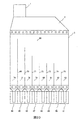
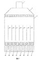
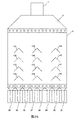
本実施例の電子装置の保護回路は第1の実施例と基本的に同じででるが、以下の変更を加えた。まず、保護抵抗3に配置したスリットを短くしている。本実施例では、保護抵抗3に、保護抵抗3の長さよりも短いスリット69~75を設けている。そうすることで、保護抵抗3に、抵抗68と電流分散抵抗76~83を構成している。
次に、本実施例の保護回路の回路図について、図18を用いて説明する。外部接続端子1は、保護抵抗3の外部接続端子1側の部分で構成される抵抗68と接続される。抵抗68は、保護抵抗3を分割して構成した電流分散抵抗76~83と接続される。そして、電流分散抵抗76~83は、MOSトランジスタ対84~91に接続される。MOSトランジスタ対84~91のゲート電極に信号を印加することで、外部接続端子1は駆動される。
次に、保護抵抗3に、抵抗68と電流分散抵抗76~83を構成していることによる効果について説明する。
外部接続端子1に印加されるサージ電圧によって流れる保護抵抗3の電流は、外部接続端子1からMOSトランジスタ対84~91に向けて直線的に流れる傾向がある。特に、外部接続端子1の近傍では、この傾向が大きい。この結果、第1の実施例の様に外部接続端子1とスリット4~10までの距離が短いと、サージ電圧による電流が保護抵抗14,15に集中する傾向がある。この傾向を下げる為に、外部接続端子1と保護抵抗3の距離を長くする方法もある。しかし、この場合、配線層2が長くなり配線層2の電流容量が低下してしまう。また、チップサイズも増大してしまう。
そこで、本実施例ではスリット69~75を保護抵抗3よりも短くしている。本実施例では、保護抵抗3の中間までしか延伸しないことで、保護抵抗3に抵抗68を更に配置している。抵抗68を配置することで、保護抵抗3や配線層2の大きさを変更することなく、外部接続端子1から電流分散抵抗76~83までの距離を確保することが可能となる。リアクタンスおよび発熱による抵抗上昇などの効果で、抵抗68を流れる電流を均一化でき、電流分散抵抗76~83への電流も均一に流すことが可能となる。その結果、保護抵抗3に、均一にサージ電流が流れる様にすることができる。なお、中間を例に述べたが、これに限られるものではない。すなわち、延伸を保護抵抗3の途中までとすることで、抵抗68を更に配置することは可能である。
スリット69~75を短くしてすることで、電流分散抵抗76~83の抵抗値は小さくなるが、配線の損傷を防ぐためにはサージ電圧の最大値と電流分散抵抗76~83の抵抗値で決まる電流値よりも配線の電流容量の方が高ければ良く、この条件はスリット69~75を短くしても十分に成り立たせることが可能である。なお、この効果はスリット69~75を、MOSトランジスタ対84~91との接続端側から延伸するように配置した場合に最大の効果を得ることができる。仮に、スリット69~75をMOSトランジスタ対84~91との接続端側から少し離した場合、この離した隙間に抵抗成分が生じ、この抵抗成分の影響で実質的な電流分散抵抗76~83の抵抗値を低下させるからである。
また、本実施例では、図16や図18に示すように、MOSトランジスタ19~26をMOSトランジスタ対84~91に置き換えている。
図16を用いてMOSトランジスタ対84、85の詳細を説明する。なお、MOSトランジスタ対86~91もMOSトランジスタ対84、85と同様な構成である。
MOSトランジスタ対84は、拡散層98にゲート電極100、102を配置してソース99、103とドレイン101を構成する。ソース99、103はグランドに接続される。ドレイン101は、配線層96、コンタクト92、93を介して電流分散抵抗76に接続される。
MOSトランジスタ対85は、拡散層98にゲート電極104、106を配置してソース103、107とドレイン105を構成する。ソース103、107はグランドに接続される。ドレイン105は、配線層97、コンタクト94、95を介して電流分散抵抗77に接続される。
この様なMOSトランジスタ対とする効果について説明する。
隣り合うMOSトランジスタのソース領域あるいはドレイン領域を共用することで、チップサイズの小型を図ることが可能となる。また、各MOSトランジスタに拡散層を個別に設ける必要が無く1つの拡散層98で複数のMOSトランジスタを配置できることからもチップサイズを小型化できる。本実施例の様に、電流分散抵抗76~83の各々にMOSトランジスタを2個接続しても、サージ電流の最大値はサージ電圧の最大値と電流分散抵抗76~83の抵抗値で決まる。つまり、電流分散抵抗76~83の各々にMOSトランジスタを複数個接続しても、サージ電流の最大値はほとんど変化しないので配線の損傷を防ぐことが可能である。
[スリット形状の改良例]
次に、図17を用いて、第1の実施例から第5の実施例で述べたスリット75の先端形状の改良例について説明する。スリット75の先端は図17に示す様に角を取った形状にした。この様にスリットの先端形状を丸めることでサージ印加に流れるサージ印加電流がスムーズに流れ、先端部分での発熱を抑えることができる。
次に、図17を用いて、第1の実施例から第5の実施例で述べたスリット75の先端形状の改良例について説明する。スリット75の先端は図17に示す様に角を取った形状にした。この様にスリットの先端形状を丸めることでサージ印加に流れるサージ印加電流がスムーズに流れ、先端部分での発熱を抑えることができる。
[第6の実施例]
次に、本発明の第6の実施例である電子装置を図19により説明する。なお、図19は第6の実施例の電子装置の保護回路の構成である。なお、第5の実施例と同様の構造については説明を省略する。
次に、本発明の第6の実施例である電子装置を図19により説明する。なお、図19は第6の実施例の電子装置の保護回路の構成である。なお、第5の実施例と同様の構造については説明を省略する。
本実施例の電子装置の保護回路は基本的に第5実施例の電子装置と同じであるが、保護抵抗3の側端部側のスリット69、75を短くし、保護抵抗3の中央部のスリット71、72、73を長くした。言い換えると、中心側のスリットよりも、側端部側のスリットを短く構成している。こうすることで、側端部側の電流分散抵抗の抵抗値を小さくなり、サージ電流がより保護抵抗3の側端部に流れやすくなる。外部接続端子1が中心側に位置する場合、サージ電流は直進傾向があるため、側端部側には流れにくくなる傾向がある。本実施例によれば、外部接続端子1から遠い(側端部側にある)電流分散抵抗の抵抗を小さくしているため、より均等にサージ電流が保護抵抗3を流れる様にできる。
[第7の実施例]
次に、本発明の第7の実施例である電子装置を図20により説明する。なお、図20は第7の実施例の電子装置の保護回路の構成である。なお、第5、第6の実施例と同様の構造については説明を省略する。
次に、本発明の第7の実施例である電子装置を図20により説明する。なお、図20は第7の実施例の電子装置の保護回路の構成である。なお、第5、第6の実施例と同様の構造については説明を省略する。
本実施例の電子装置の保護回路は基本的に第5実施例の電子装置と同じであるが、外部接続端子1が左側に偏った構成になっている。そして、保護抵抗3の側端部のスリット75を短くし、外部接続端子1に近いスリット69、70、71を長くした。こうすることで、サージ電流がより保護抵抗3の右側に流れやすくなる。本実施例によれば、外部接続端子1から遠い(右側端部側にある)電流分散抵抗の抵抗を小さくしているため、より均等にサージ電流が保護抵抗3を流れる様にできる。この結果、外部接続端子1が左側に偏ったとしてもサージ電流がより均等に保護抵抗3の内部を流れる様にできる。右側に外部端子1が設けられた場合も同様である。
[第8の実施例]
本発明の第8の実施例である電子装置を図21により説明する。なお、第5の実施例と同様の構成については説明を省略する。
本発明の第8の実施例である電子装置を図21により説明する。なお、第5の実施例と同様の構成については説明を省略する。
本実施例の電子装置の保護回路は基本的に第5実施例の電子装置と同じであるが、スリット69~75をMOSトランジスタ対84~91との接続端から離した。こうした場合でも、本保護回路の等価回路は第5の実施例で示した図18の回路図と同じになる。つまり、第5の実施例と同様にサージ電圧が印加された時に流れるサージ電流がより均等に保護抵抗3の内部を流れる様にでき、且つ、サージ電圧が印加された時に流れるサージ電流によってMOSトランジスタ対84~91への接続配線が損傷することを防ぐことができる。
[第9の実施例]
本発明の第9の実施例である電子装置を図22により説明する。なお、第5の実施例と同様の構成については説明を省略する。
本発明の第9の実施例である電子装置を図22により説明する。なお、第5の実施例と同様の構成については説明を省略する。
本実施例の電子装置の保護回路は基本的に第5実施例の電子装置と同じであるが、スリット69、71、73、75を削除してスリットの本数を少なくした。こうした場合でも、サージ電圧が印加された時にMOSトランジスタ対84~91へ流れる電流を制限することができる。この結果、サージ電圧が印加された時に流れるサージ電流によりMOSトランジスタ対84~91への接続配線が損傷することを防ぐことができる。つまり、スリット70、72、74で、MOSトランジスタ対84、85の接続箇所と、MOSトランジスタ対86、87の接続箇所と、MOSトランジスタ対88、89の接続箇所と、MOSトランジスタ対90、91の接続箇所に分割することで、サージ電圧が印加された時にMOSトランジスタ対84~91へ流れる電流を制限することができる。また、別の言い方をすれば、スリット70、72、74で保護抵抗3を分割して電流分散抵抗を複数構成して、この電流分散抵抗をMOSトランジスタ対84、85とMOSトランジスタ対86、87とMOSトランジスタ対88、89とMOSトランジスタ対90、91に接続する。そうすることで、サージ電圧が印加された時にMOSトランジスタ対84~91へ流れる電流を制限することができる。この結果、サージ電圧が印加された時に流れるサージ電流により、MOSトランジスタ対84~91への接続配線が損傷することを防ぐことができる。
[第10の実施例]
次に、本発明の第10の実施例である電子装置を図23により説明する。なお、第5の実施例と同様の構成については説明を省略する。
次に、本発明の第10の実施例である電子装置を図23により説明する。なお、第5の実施例と同様の構成については説明を省略する。
本実施例の電子装置の保護回路は基本的に第5実施例の電子装置と同じであるが、スリット69~75を、連続する穴の列108~114に置き換えた。こうした場合でも、本保護回路の等価回路は第5の実施例で示した図18の回路図と同じになる。
[第11の実施例]
次に、本発明の第11の実施例である電子装置を図24により説明する。なお、第5の実施例と同様の構成については説明を省略する。
次に、本発明の第11の実施例である電子装置を図24により説明する。なお、第5の実施例と同様の構成については説明を省略する。
本実施例の電子装置の保護回路は基本的に第5実施例の電子装置と同じであるが、スリット69~75を斜め方向に配置したスリット115~130に置き換えた。こうした場合でも、本保護回路の等価回路は第5の実施例で示した図18の回路図と同じになる。
[第12の実施例]
次に、本発明の第12の実施例である電子装置を図25により説明する。なお、第11の実施例と同様の構成については説明を省略する。
次に、本発明の第12の実施例である電子装置を図25により説明する。なお、第11の実施例と同様の構成については説明を省略する。
本実施例の電子装置の保護回路は基本的に第11実施例の電子装置と同じであるが、スリット115~130を、山形のスリット131~142に置き換えた。こうした場合でも、本保護回路の等価回路は第5の実施例で示した図18の回路図と同じになる。
[第13の実施例]
次に、本発明の第13の実施例である電子装置を図26、27により説明する。なお、第5の実施例と同様の構成については説明を省略する。
次に、本発明の第13の実施例である電子装置を図26、27により説明する。なお、第5の実施例と同様の構成については説明を省略する。
本実施例の電子装置の保護回路は基本的に第5実施例の電子装置と同じであるが、配線層143を追加し、コンデンサ144を配置し、AD変換器などの内部回路145に接続した。
本実施例では、抵抗68とコンデンサ144でフィルタを構成することができる。フィルタを配置することで外部接続端子1から入ってくるサージ電圧や高周波ノイズをこのフィルタで減衰させることができ、内部回路145の安定化を図ることができる。つまり、本実施例ではサージ電圧保護とフィルタ機能達成の為に使用する抵抗として抵抗68を共用することでチップサイズを小型化できる。
先述したように、保護抵抗3は、シリコン基板29と酸化膜28により絶縁されている。この結果、外部接続端子1に印加される正電位および負電位のサージに対して絶縁性を確保している。この為、本実施例のフィルタは、外部接続端子1に電源電圧以上あるいはグランド電圧以下の電圧が入力されたとしても平均値を維持する。つまり、外部接続端子1にサージ等の高電圧が印加されたとしても、本実施例のフィルタは正常に動作することができる。
また、配線層143から内部回路145に信号を取り込んだ場合、外部接続端子1と内部回路145の間には抵抗68が直列に入り、電流分散抵抗76~83とMOSトランジスタ対84~91の直列回路がグランドに並列に入る。この為、配線層143の信号、つまり、内部回路145への入力信号は抵抗68と電流分散抵抗76~83とMOSトランジスタ対84~91で構成されるサージ保護回路で保護される。特に、抵抗68が入ることでより高いサージ電圧の減衰効果を得ることができ、サージ電圧に弱い内部回路145をより強く保護することができる。この結果、内部回路145のサージ電圧による破壊や誤動作を防ぐことができるので、より信頼性の高い電子装置を提供できる。
[第14の実施例]
次に、本発明の第14の実施例である電子装置を図28により説明する。なお、図28は第14の実施例の電子装置の保護回路の構成である。
次に、本発明の第14の実施例である電子装置を図28により説明する。なお、図28は第14の実施例の電子装置の保護回路の構成である。
本実施例の電子装置の保護回路は基本的に第1実施例の電子装置と同じであるが、配線層145を追加した。本保護回路の等価回路は第13の実施例で示した図27の回路図と基本的に同じなので、第13の実施例と同様にサージ電圧が印加された時に流れるサージ電流がより均等に保護抵抗3の内部を流れる様にでき、且つ、サージ電圧が印加された時に流れるサージ電流によってMOSトランジスタ19~26への接続配線が損傷することを防ぐことができる。また、配線層146を付加することで等価的に抵抗68を実現できるので、コンデンサ144を接続することでフィルタを構成できる様にした。フィルタを配置することで外部接続端子1から入ってくるサージ電圧や高周波ノイズをこのフィルタで減衰させることができる。この結果、内部回路145のサージ電圧による破壊や誤動作を防ぐことができるので、より信頼性の高い電子装置を提供できる。
上述した何れの実施例では、保護抵抗に形成されるパターン部としてスリットを例に説明したが、溝であっても同様の効果を奏する。同様に、保護抵抗に形成されるパターン部として連続する孔を例に説明したが、連続する凹みであっても同様の効果を奏する。また、これらのパターン部は、成膜した後にエッチング等により形成する構成に限定されず、マスキングにより成膜時に形成する等の他の構成も当然ながら含まれる。
1‥外部接続端子、2‥配線層、3‥保護抵抗、4‥スリット、5‥スリット、6‥スリット、7‥スリット、8‥スリット、9‥スリット、10‥スリット、11‥電流分散抵抗、12‥電流分散抵抗、13‥電流分散抵抗、14‥電流分散抵抗、15‥電流分散抵抗、16‥電流分散抵抗、17‥電流分散抵抗、18‥電流分散抵抗、19‥MOSトランジスタ、20‥MOSトランジスタ、21‥MOSトランジスタ、22‥MOSトランジスタ、23‥MOSトランジスタ、24‥MOSトランジスタ、25‥MOSトランジスタ、26‥MOSトランジスタ、27‥コンタクト、28‥酸化膜、29‥シリコン基板、30‥コンタクト、31‥コンタクト、32‥コンタクト、33‥コンタクト、34‥配線層、35‥配線層、36‥拡散層、37‥ソース、38‥ゲート電極、39‥ドレイン、40‥ソース、41‥ゲート電極、42‥ドレイン、43‥拡散層、44‥MOSダイオード、45‥MOSダイオード、46‥MOSダイオード、47‥MOSダイオード、48‥MOSダイオード、49‥MOSダイオード、50‥MOSダイオード、51‥MOSダイオード、52‥バイポーラトランジスタ、53‥バイポーラトランジスタ、54‥バイポーラトランジスタ、55‥バイポーラトランジスタ、56‥バイポーラトランジスタ、57‥バイポーラトランジスタ、58‥バイポーラトランジスタ、59‥バイポーラトランジスタ、60‥ダイオード、61‥ダイオード、62‥ダイオード、63‥ダイオード、64‥ダイオード、65‥ダイオード、66‥ダイオード、67‥ダイオード、68‥抵抗、69‥スリット、70‥スリット、71‥スリット、72‥スリット、73‥スリット、74‥スリット、75‥スリット、76‥電流分散抵抗、77‥電流分散抵抗、78‥電流分散抵抗、79‥電流分散抵抗、80‥電流分散抵抗、81‥電流分散抵抗、82‥電流分散抵抗、83‥電流分散抵抗、84‥MOSトランジスタ対、85‥MOSトランジスタ対、86‥MOSトランジスタ対、87‥MOSトランジスタ対、88‥MOSトランジスタ対、89‥MOSトランジスタ対、90‥MOSトランジスタ対、91‥MOSトランジスタ対、92‥コンタクト、93‥コンタクト、94‥コンタクト、95‥コンタクト、96‥配線層、97‥配線層、98‥拡散層、99‥ソース、100‥ゲート電極、101‥ドレイン、102‥ゲート電極、103‥ソース、104‥ゲート電極、105‥ドレイン、106‥ゲート電極、107‥ソース、108‥連続する穴の列、109‥連続する穴の列、110‥連続する穴の列、111‥連続する穴の列、112‥連続する穴の列、113‥連続する穴の列、114‥連続する穴の列、115‥スリット、116‥スリット、117‥スリット、118‥スリット、119‥スリット、120‥スリット、121‥スリット、122‥スリット、123‥スリット、124‥スリット、125‥スリット、126‥スリット、127‥スリット、128‥スリット、129‥スリット、130‥スリット、131‥スリット、132‥スリット、133‥スリット、134‥スリット、135‥スリット、136‥スリット、137‥スリット、138‥スリット、139‥スリット、140‥スリット、141‥スリット、142‥スリット、143‥配線層、144‥コンデンサ、145‥内部回路、146‥配線層
Claims (14)
- 外部接続端子と、前記外部接続端子に接続される保護抵抗と、前記保護抵抗に接続される複数の半導体素子と、を備え、前記複数の半導体素子は、並列接続されている半導体デバイスを有する電子装置において、
前記保護抵抗は、スリット、溝、連続する孔、連続する凹みの少なくとも何れかで形成されるパターン部を有する電子装置 - 前記パターン部は、前記保護抵抗に流れる電流の通電方向に沿うように設けられる請求項1に記載の電子装置
- 前記パターン部は、前記保護抵抗の前記複数の半導体素子との接続端側から延伸するように形成される請求項2に記載の電子装置
- 前記パターン部は、前記保護抵抗の途中まで延伸するように形成される請求項3に記載の電子装置
- 前記パターン部は、複数のスリット、複数の溝、複数の連続する孔、複数の連続する凹みの少なくとも何れかを有する請求項1乃至4の何れかに記載の電子装置
- 前記パターン部は、前記保護抵抗の側端部に近い方が短くなるように形成されている請求項5に記載の電子装置
- 前記パターン部は、前記保護抵抗の前記外部接続端子に近い方が長くなるように形成した請求項5に記載の電子装置
- 前記スリットは、端部の角を取った形状である請求項5電子装置
- 前記パターン部は、前記複数の半導体素子と前記保護抵抗の接続箇所を複数に分割するように前記複数のスリット、前記複数の溝、前記複数の連続する孔、前記複数の連続する凹みの少なくとも何れかを配置した請求項5に記載の電子装置
- 前記複数の半導体素子はMOSトランジスタ、バイポーラトランジスタ、ダイオードなどの降伏特性を持つ半導体素子である請求項1に記載の電子装置
- 複数のスリット、若しくは複数の溝、若しくは複数の連続する孔、若しくは複数の連続する凹みにより前記保護抵抗を分割することで電流分散抵抗を複数構成し、前記電流分散抵抗を前記複数の半導体素子に接続した請求項4に記載の電子装置
- 前記電流分散抵抗上に電気的接続部を設ける請求項11に記載の電子装置
- 前記電気的接続部から電気信号を取り出し、内部回路へ電気信号を取り出した請求項12に記載の電子装置
- 前記電気的接続部から電気信号を取り出し、コンデンサと接続した請求項12に記載の電子装置
Priority Applications (3)
| Application Number | Priority Date | Filing Date | Title |
|---|---|---|---|
| DE112017005287.4T DE112017005287B4 (de) | 2017-01-19 | 2017-12-20 | Elektronische Vorrichtung |
| CN201780071699.2A CN110168715B (zh) | 2017-01-19 | 2017-12-20 | 电子装置 |
| US16/461,684 US11043485B2 (en) | 2017-01-19 | 2017-12-20 | Electronic device having semiconductor device with protective resistor |
Applications Claiming Priority (2)
| Application Number | Priority Date | Filing Date | Title |
|---|---|---|---|
| JP2017007160A JP6838240B2 (ja) | 2017-01-19 | 2017-01-19 | 電子装置 |
| JP2017-007160 | 2017-01-19 |
Publications (1)
| Publication Number | Publication Date |
|---|---|
| WO2018135220A1 true WO2018135220A1 (ja) | 2018-07-26 |
Family
ID=62909201
Family Applications (1)
| Application Number | Title | Priority Date | Filing Date |
|---|---|---|---|
| PCT/JP2017/045673 Ceased WO2018135220A1 (ja) | 2017-01-19 | 2017-12-20 | 電子装置 |
Country Status (5)
| Country | Link |
|---|---|
| US (1) | US11043485B2 (ja) |
| JP (1) | JP6838240B2 (ja) |
| CN (1) | CN110168715B (ja) |
| DE (1) | DE112017005287B4 (ja) |
| WO (1) | WO2018135220A1 (ja) |
Citations (10)
| Publication number | Priority date | Publication date | Assignee | Title |
|---|---|---|---|---|
| JPS5916364A (ja) * | 1982-07-19 | 1984-01-27 | Hitachi Ltd | Mis形半導体icの信号入力回路 |
| JPS6042856A (ja) * | 1983-08-18 | 1985-03-07 | Toshiba Corp | 半導体集積回路 |
| JPS60136359A (ja) * | 1983-12-26 | 1985-07-19 | Hitachi Ltd | 半導体集積回路装置 |
| JPS6393870A (ja) * | 1986-10-07 | 1988-04-25 | Ricoh Co Ltd | 薄膜形成装置 |
| JPH0217669A (ja) * | 1988-07-05 | 1990-01-22 | Mitsubishi Electric Corp | 半導体装置 |
| JPH02273971A (ja) * | 1989-03-13 | 1990-11-08 | Philips Gloeilampenfab:Nv | 保護回路をそなえた半導体デバイス |
| JPH11312783A (ja) * | 1998-04-27 | 1999-11-09 | Mitsubishi Electric Corp | 半導体集積回路装置 |
| JP2005167049A (ja) * | 2003-12-04 | 2005-06-23 | Nec Electronics Corp | 半導体集積回路装置 |
| JP2005303051A (ja) * | 2004-04-13 | 2005-10-27 | Ricoh Co Ltd | 半導体装置及びその製造方法 |
| JP2010028109A (ja) * | 2008-06-17 | 2010-02-04 | Semiconductor Energy Lab Co Ltd | 半導体装置 |
Family Cites Families (11)
| Publication number | Priority date | Publication date | Assignee | Title |
|---|---|---|---|---|
| JPH0215746U (ja) * | 1988-07-15 | 1990-01-31 | ||
| US5248892A (en) | 1989-03-13 | 1993-09-28 | U.S. Philips Corporation | Semiconductor device provided with a protection circuit |
| US6583972B2 (en) * | 2000-06-15 | 2003-06-24 | Sarnoff Corporation | Multi-finger current ballasting ESD protection circuit and interleaved ballasting for ESD-sensitive circuits |
| JP3879063B2 (ja) * | 2002-06-11 | 2007-02-07 | 富士通株式会社 | 半導体装置およびその製造方法 |
| CN1992266A (zh) * | 2005-12-27 | 2007-07-04 | 松下电器产业株式会社 | 半导体集成电路装置 |
| JP2011096897A (ja) | 2009-10-30 | 2011-05-12 | Renesas Electronics Corp | 半導体装置及び電子機器 |
| US9627467B2 (en) * | 2013-09-06 | 2017-04-18 | Taiwan Semiconductor Manufacturing Company, Ltd. | Thin film resistor integrated between interconnect levels and contacting an underlying dielectric layer protrusion |
| NL2016900B1 (en) * | 2016-06-06 | 2017-12-13 | Fortimedix Surgical B V | Steerable instrument comprising a cylindrical diameter adaptation section |
| CN109690703B (zh) * | 2016-12-16 | 2021-06-04 | 松下知识产权经营株式会社 | 芯片电阻器及其制造方法 |
| JP2020053537A (ja) * | 2018-09-26 | 2020-04-02 | パナソニック株式会社 | 太陽電池セル及び太陽電池セルの製造方法 |
| WO2020168449A1 (en) * | 2019-02-18 | 2020-08-27 | Yangtze Memory Technologies Co., Ltd. | Channel hole and bitline architecture and method to improve page or block size and performance of 3d nand |
-
2017
- 2017-01-19 JP JP2017007160A patent/JP6838240B2/ja active Active
- 2017-12-20 CN CN201780071699.2A patent/CN110168715B/zh active Active
- 2017-12-20 WO PCT/JP2017/045673 patent/WO2018135220A1/ja not_active Ceased
- 2017-12-20 US US16/461,684 patent/US11043485B2/en active Active
- 2017-12-20 DE DE112017005287.4T patent/DE112017005287B4/de active Active
Patent Citations (10)
| Publication number | Priority date | Publication date | Assignee | Title |
|---|---|---|---|---|
| JPS5916364A (ja) * | 1982-07-19 | 1984-01-27 | Hitachi Ltd | Mis形半導体icの信号入力回路 |
| JPS6042856A (ja) * | 1983-08-18 | 1985-03-07 | Toshiba Corp | 半導体集積回路 |
| JPS60136359A (ja) * | 1983-12-26 | 1985-07-19 | Hitachi Ltd | 半導体集積回路装置 |
| JPS6393870A (ja) * | 1986-10-07 | 1988-04-25 | Ricoh Co Ltd | 薄膜形成装置 |
| JPH0217669A (ja) * | 1988-07-05 | 1990-01-22 | Mitsubishi Electric Corp | 半導体装置 |
| JPH02273971A (ja) * | 1989-03-13 | 1990-11-08 | Philips Gloeilampenfab:Nv | 保護回路をそなえた半導体デバイス |
| JPH11312783A (ja) * | 1998-04-27 | 1999-11-09 | Mitsubishi Electric Corp | 半導体集積回路装置 |
| JP2005167049A (ja) * | 2003-12-04 | 2005-06-23 | Nec Electronics Corp | 半導体集積回路装置 |
| JP2005303051A (ja) * | 2004-04-13 | 2005-10-27 | Ricoh Co Ltd | 半導体装置及びその製造方法 |
| JP2010028109A (ja) * | 2008-06-17 | 2010-02-04 | Semiconductor Energy Lab Co Ltd | 半導体装置 |
Also Published As
| Publication number | Publication date |
|---|---|
| US11043485B2 (en) | 2021-06-22 |
| CN110168715B (zh) | 2023-07-18 |
| DE112017005287B4 (de) | 2023-01-12 |
| US20190355714A1 (en) | 2019-11-21 |
| CN110168715A (zh) | 2019-08-23 |
| DE112017005287T5 (de) | 2019-07-11 |
| JP2018117053A (ja) | 2018-07-26 |
| JP6838240B2 (ja) | 2021-03-03 |
Similar Documents
| Publication | Publication Date | Title |
|---|---|---|
| JP5449676B2 (ja) | 静電気放電保護装置 | |
| US7183612B2 (en) | Semiconductor device having an electrostatic discharge protecting element | |
| KR19990078148A (ko) | 반도체장치 | |
| JP3949647B2 (ja) | 半導体集積回路装置 | |
| JP6398696B2 (ja) | 静電気保護回路及び半導体集積回路装置 | |
| KR101018709B1 (ko) | 반도체 소자의 핀 저항 조절용 다이오드 | |
| JP2008147338A (ja) | 半導体集積回路装置 | |
| JP6514949B2 (ja) | オンチップノイズ保護回路を有する半導体チップ | |
| JP2012049444A (ja) | 保護回路および半導体装置 | |
| KR102158458B1 (ko) | 반도체 장치 | |
| JP6405986B2 (ja) | 静電気保護回路及び半導体集積回路装置 | |
| CN103094277B (zh) | 半导体装置 | |
| JP6838240B2 (ja) | 電子装置 | |
| KR20070065271A (ko) | 반도체 장치 | |
| KR100699845B1 (ko) | 액티브 영역의 면적을 감소시킨 반도체 메모리 장치 | |
| CN110137169A (zh) | 半导体装置 | |
| KR100952245B1 (ko) | 정전기 방전 보호회로 및 그 제조 방법 | |
| US7417287B2 (en) | Electrostatic discharge device having controllable trigger voltage | |
| JP6796034B2 (ja) | 半導体装置 | |
| CN100403535C (zh) | 可控制触发电压的静电放电装置 | |
| JP5455151B2 (ja) | 半導体装置 | |
| US7049698B1 (en) | Semiconductor integrated circuit having transistor with reduced resistance | |
| JP2004200650A (ja) | 静電気放電保護素子 | |
| JP2005317759A (ja) | 半導体装置 | |
| KR20130090576A (ko) | 드라이버 트랜지스터를 구비하는 반도체 집적 회로 장치 |
Legal Events
| Date | Code | Title | Description |
|---|---|---|---|
| 121 | Ep: the epo has been informed by wipo that ep was designated in this application |
Ref document number: 17893425 Country of ref document: EP Kind code of ref document: A1 |
|
| 122 | Ep: pct application non-entry in european phase |
Ref document number: 17893425 Country of ref document: EP Kind code of ref document: A1 |