US6583972B2 - Multi-finger current ballasting ESD protection circuit and interleaved ballasting for ESD-sensitive circuits - Google Patents
Multi-finger current ballasting ESD protection circuit and interleaved ballasting for ESD-sensitive circuits Download PDFInfo
- Publication number
- US6583972B2 US6583972B2 US09/881,422 US88142201A US6583972B2 US 6583972 B2 US6583972 B2 US 6583972B2 US 88142201 A US88142201 A US 88142201A US 6583972 B2 US6583972 B2 US 6583972B2
- Authority
- US
- United States
- Prior art keywords
- source
- terminal
- circuit
- transistor
- drain
- Prior art date
- Legal status (The legal status is an assumption and is not a legal conclusion. Google has not performed a legal analysis and makes no representation as to the accuracy of the status listed.)
- Expired - Lifetime, expires
Links
Images


Classifications
-
- H—ELECTRICITY
- H01—ELECTRIC ELEMENTS
- H01L—SEMICONDUCTOR DEVICES NOT COVERED BY CLASS H10
- H01L27/00—Devices consisting of a plurality of semiconductor or other solid-state components formed in or on a common substrate
- H01L27/02—Devices consisting of a plurality of semiconductor or other solid-state components formed in or on a common substrate including semiconductor components specially adapted for rectifying, oscillating, amplifying or switching and having at least one potential-jump barrier or surface barrier; including integrated passive circuit elements with at least one potential-jump barrier or surface barrier
- H01L27/0203—Particular design considerations for integrated circuits
- H01L27/0248—Particular design considerations for integrated circuits for electrical or thermal protection, e.g. electrostatic discharge [ESD] protection
- H01L27/0251—Particular design considerations for integrated circuits for electrical or thermal protection, e.g. electrostatic discharge [ESD] protection for MOS devices
- H01L27/0266—Particular design considerations for integrated circuits for electrical or thermal protection, e.g. electrostatic discharge [ESD] protection for MOS devices using field effect transistors as protective elements
-
- H—ELECTRICITY
- H01—ELECTRIC ELEMENTS
- H01L—SEMICONDUCTOR DEVICES NOT COVERED BY CLASS H10
- H01L2924/00—Indexing scheme for arrangements or methods for connecting or disconnecting semiconductor or solid-state bodies as covered by H01L24/00
- H01L2924/0001—Technical content checked by a classifier
- H01L2924/0002—Not covered by any one of groups H01L24/00, H01L24/00 and H01L2224/00
Definitions
- the present invention relates to electrostatic discharge (ESD) protection, and, more particularly, to ESD protection circuits for reducing the voltage stress on integrated circuits during an ESD event.
- ESD electrostatic discharge
- ESD electrostatic discharge
- ICs Integrated circuits
- MOS metal-oxide semiconductor
- I/O input/output
- power pins or other pads of the IC which can damage sensitive semiconductor junctions, dielectrics, interconnections or other sub-elements of the IC.
- ESD protection circuits or structures may, for example, be placed in parallel across two input pins or pads, such as an I/O pad and ground, and therefore also in parallel across sensitive circuitry coupled to the two pads.
- ESD protection is unobtrusive or “invisible” to the normal operation of the circuit, so that its presence does not slow down or otherwise negatively impact the operation of the remaining IC circuitry when no ESD event is occurring.
- ESD protection structures Two commonly-used ESD protection structures are the SCR (silicon or semiconductor controlled rectifiers), and the npn bipolar transistor. Both types of structures exhibit a low-voltage, low-resistance state (known as the holding or clamping voltage) when a certain triggering voltage (or current) has been reached. Usually, the triggering voltage is higher than the holding voltage. Unless specifically designed otherwise, the SCR usually has the lowest holding voltage.
- SCRs have been used, both parasitically and deliberately, to protect ICs, such as the SCR techniques described in U.S. Pat. Nos. 4,400,711, 4,405,933, 4,631,567 and 4,692,781.
- the major advantage of these SCR protection structures is their high energy-absorbing capability.
- various forms of protection structures have been built around the npn snap-back phenomenon, such as the structures and techniques described in U.S. Pat. No. 5,519,242.
- This and similar structures take advantage of the parasitic npn bipolar junction transistor (BJT) existing in every NMOS transistor.
- BJT parasitic npn bipolar junction transistor
- ggNMOS grounded-gate NMOS
- ESD protection device widths may be used to protect against large ESD events.
- large device widths are achieved by using a multi-finger layout.
- a major concern with regard to multi-finger devices under ESD stress is the possibility of non-uniform triggering of the fingers.
- Curves 102 and 103 of FIG. 1 illustrate the behavior of a single parasitic BJT. When the voltage across the BJT exceeds V t1 , the BJT operates in a snapback mode to conduct current, thus, reducing the voltage across the protected circuitry. As shown by the curves 102 and 103 in FIG.
- V t2 the voltage value at failure, V t2 , must exceed the triggering voltage V t1 of the parasitic BJT transistor, i.e. the voltage at the onset of snapback. This ensures that a second parallel finger will trigger at around V t1 , before the first conducting finger reaches V t2 . Thus, damage to an initially triggered and first conducting finger can be avoided until adjacent fingers are also switched on into the low resistive ESD conduction state (i.e. snapback). To achieve the condition V t1 ⁇ V t2 either the triggering voltage must be reduced or the second breakdown voltage must be increased.
- the ESD trigger voltage V t1 decreases to V t1 ′, toward the snapback holding voltage V h intrinsically situated below V t2 .
- the transient biasing is designed to be present for a time interval sufficient to cause all parallel fingers to fully conduct the ESD current.
- the gate coupling and/or substrate triggering generally change the NMOS high current characteristic from the curves 102 and 103 to the curves 104 and 103 .
- these techniques also make it possible for NMOS transistors with a characteristic represented by curves 102 and 105 , which may be inappropriate for ESD protection, to be modified to have a more appropriate characteristic represented by curves 104 and 105 .
- a general drawback of these methods, in particular with regard to radio frequency (RF) applications is the relatively large additional capacitance which is introduced at the I/O pads.
- Another drawback is the design complexity of the dynamic biasing circuitry which is typically designed to handle ESD events having many different time signatures.
- V t2 One method for increasing V t2 is to add ballasting resistance, e.g. by an increase of the drain contact to gate spacing in conjunction with silicide blocking as shown in FIG. 4 A.
- ballasting resistance e.g. by an increase of the drain contact to gate spacing in conjunction with silicide blocking as shown in FIG. 4 A.
- the fully silicided multi-finger NMOS device (FIGS. 4B and 4D) is susceptible to ESD currents because no ballasting resistance is available.
- the introduction of fully silicided regions (FIG. 4C) in the drain and source region leads to very large device dimensions without evidence of actual improvement of the ESD device performance. Again, additional capacitance is added in form of junction capacitance by the increased drain area.
- ballast resistance is the increased holding voltage under high current conduction. This leads to a higher power dissipation and thus inherently to a lower ESD performance. This also leads to a higher voltage build-up across the protection device and, thus, across the protected circuit node.
- Another general drawback of adding ballast resistance is the reduction of NMOS drive current and speed for normal operating conditions.
- an ESD protection circuit or clamp it is therefore desirable for an ESD protection circuit or clamp to have a known multi-finger performance without using dynamic biasing and in implementations that do not add either additional capacitance or additional ballast resistance. Furthermore, it is desirable to have an ESD performance that varies as a linear function of the structure width.
- the present invention is embodied in a multi-finger ESD protection circuit having at least two first resistive channels defining input fingers.
- First and second field effect transistors (FETs) each having drain, source and gate terminals are includes.
- Each of the first and second FETs defines a respective parasitic bipolar junction transistor (BJT) between the first and second circuit terminals.
- the base of the BJT corresponds to the channel region of the FET.
- the drain (collector) terminals of the first and second FETs are connected to a corresponding one of the at least two input fingers.
- the gate terminal of the first FET is connected to the gate terminal of the second FET.
- the gate terminal of the first FET is coupled to the channel of the first FET and to the channel of the second FET.
- the multi-finger ESD protection circuit further includes at least two second resistive channels connected between corresponding ones of the source (emitter) terminals of the at least two FETs and a source of reference potential.
- a multi-finger ESD protection has a plurality of first resistive channels defining respective input fingers.
- a respective plurality of field effect transistors (FETs), including first, second and last FETs, each having drain, source and gate terminals, are included, the drain terminals of the plurality of FETs are connected to respective ones of the plurality of input fingers.
- Each of the plurality of FETs defines a respective parasitic bipolar junction transistor between the first and second circuit terminals.
- the gate terminal of the second FET is connected to the source terminal of the first FET and the gate terminal of the first FET is connected to the source terminal of the last FET.
- a respective plurality of second resistive channels are connected between a corresponding one of the source terminals of the plurality of FETs and a source of reference potential.
- a multi-finger ESD protection circuit in which each FET has a channel region that corresponds to the base electrode of the parasitic bipolar transistor and the channel region of the second FET is coupled to the source terminal of the first FET.
- the FET has a channel region that corresponds to the base electrode of the parasitic bipolar transistor and the gate terminal of the second FET is connected to the channel region of the second FET and to the source terminal of the first FET.
- a gate biasing circuit in which a biasing circuit is operably linked to a plurality of parallel-connected FETs to simultaneously bias the plurality of FETs to uniformly distribute current flow between the first and second circuit terminals, among the plurality of FETs during an ESD event.
- the biasing circuit includes a further FET including gate, source and drain electrodes is configured with its source electrode coupled to the first circuit terminal and its drain electrode coupled to interconnected gate electrodes of the plurality of parallel-connected FETs.
- the circuit further includes a plurality of triggering FETs, each configured with a source electrode coupled to the second circuit terminal, a drain electrode coupled to the gate electrode of the further FET and gate electrode coupled to the source electrode of a respective one of the plurality of parallel connected FETs.
- a diode gate coupling circuit for discharging an ESD event.
- the diodes are connected so that an anode is connected to a source terminal of one of the FETs, the cathodes are connected to the gate electrode of a first and at least a second FET of the parallel-connected FETs.
- a triggering circuit is used to detect an ESD event and produce a detection signal.
- a transfer circuit is responsive to the detection signal of the triggering circuit for producing a bias signal.
- a multi-finger ESD protection circuit including a single plurality of parallel ballasting resistors.
- Each of the plurality of ballasting resistors has a first terminal coupled to the first circuit terminal and a second terminal coupled to respective drain electrodes of a plurality of FETs.
- the source terminals of the plurality of FETs are connected to the second circuit terminal.
- FIGS. 1, 2 and 3 are graphs of the current (I) vs. voltage (V) of ESD devices which are useful for describing the operation of the subject invention
- FIG. 4A is a top plan view of a prior art MOS device layout with local blocking of silicide
- FIG. 4B is a top plan view of a prior art MOS device layout fully silicided and having minimum dimensions
- FIG. 4C is a top plan view of a prior art MOS device layout fully silicided and having additional spacings;
- FIG. 4D is a top plan view of a prior art multi-finger MOS device with silicide blocking
- FIG. 5 is top plan view, partly in schematic diagram form, which illustrates a device layout of a fully silicided current ballasting ESD protection circuit
- FIG. 6A is a top plan view of a prior art ESD protection circuit which uses vertically meandering vias and connection layers to form parallel ballasting resistors.
- FIG. 6B is a cross sectional view of one of the vertically meandering strips shown in FIG. 6A and a portion of an active device coupled to the strip;
- FIG. 6C is a top plan view of a prior art ESD protection circuit which uses parallel silicided polysilicon strips to form parallel ballasting resistors.
- FIG. 7 is a schematic diagram of a multi-finger device in accordance with a first embodiment of the present invention.
- FIG. 8A is a schematic diagram of a second embodiment of the present invention which uses a source-substrate biasing arrangement
- FIG. 8B is a schematic diagram of a third embodiment of the present invention which uses a combined source-gate-substrate biasing arrangement
- FIG. 8C is a schematic diagram of a fourth embodiment of the present invention which uses a source-gate biasing arrangement
- FIG. 8D is a schematic diagram of a fifth embodiment of the present invention which uses a source-gate biasing arrangement and a segmented source resistance.
- FIG. 9 is a device layout of a multi-finger NMOS device using the source-gate biasing arrangement of FIG. 8D;
- FIG. 10 is a device layout of a multi-finger NMOS device using the source-gate-substrate biasing arrangement of FIG. 8B;
- FIG. 11 is a schematic diagram of a sixth embodiment of the present invention having simultaneous gate biasing
- FIG. 12 is a schematic diagram of a seventh embodiment of the invention having simultaneous gate biasing
- FIG. 13 is a schematic diagram of an eighth embodiment of the invention including a diode gate control network
- FIG. 14 is a schematic diagram of an ninth embodiment of the invention including multi-finger turn-on transistors (MFT), a trigger circuit and a transfer circuit;
- MFT multi-finger turn-on transistors
- FIG. 15 is a schematic diagram of a tenth embodiment of the invention including a trigger circuit and a MFT circuit;
- FIG. 16 is top plan view which shows a device layout of a MFT device which uses a gate-substrate coupling technique
- FIG. 17A is a top plan view which shows a device layout of a plurality of parallel connected devices which use a gate-substrate coupling technique
- FIG. 17B is a schematic diagram which is useful for describing the structure shown in FIG. 17 A.
- FIG. 18 is a top plan view which shows a device layout of a plurality of parallel connected MFT devices in an in-line arrangement which use a gate-substrate coupling technique
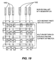
- FIG. 19 is a circuit diagram of a back end ballast (BEB) MFT structure.
- FIG. 20 is a top plan view, partially in schematic diagram form of an exemplary MFT structure.
- FIG. 21 is a schematic diagram which is useful for describing the structure shown in FIG. 20 .
- FIG. 22 is a layout diagram of the MFT structure shown in FIG. 20 .
- FIG. 23 is a top plan view, partially in schematic diagram form of an exemplary area efficient MFT structure.
- FIG. 24 is a layout diagram which is useful for describing the MFT structure shown in FIG. 23 .
- FIG. 25 is a layout diagram of the MFT structure shown in FIGS. 23 and
- FIGS. 26A and 26B are layout diagrams showing a comparison of the MFT structures shown in FIGS. 20 and 23.
- FIG. 27A is a top-plan view, partly in schematic diagram form, of an exemplary ESD protection device.
- FIG. 27B is a top plan view of a portion of the ESD protection device shown in FIG. 27 A.
- the present invention is embodied in a multi-finger turn-on (MFT) ESD protection device in which, after a first transistor has been turned on by the ESD event, the remaining transistors are biased to turn on at a lower voltage than the turn-on voltage for the first transistor.
- MFT multi-finger turn-on
- CMOS complementary metal-oxide-semiconductor
- the present invention may be applied in technologies other than CMOS-based ICs.
- the present invention may also be employed to protect NMOS-based ICs or pure bipolar-based ICs. It may also be used as a trigger circuit for SCR-based protection circuits, as will be appreciated.
- silicon ballasting resistance may be introduced to ensure equal current spreading and uniform multi-finger ESD performance (i.e., more than one MOSFET M).
- further trigger circuits are introduced to enhance multi-finger triggering and ESD performance.
- trigger circuits are not used to uniformly trigger the multi-finger MOS circuit.
- at least one transistor finger is allowed to trigger naturally.
- a bias signal is obtained to turn on the non-conducting transistor fingers.
- All techniques of the present invention fulfill the multi-finger uniform performance condition V′ t1 ⁇ V′ t2 ⁇ V t2 shown in FIG. 1A, without a specific condition required for the relationship of V t1 to V t2 or V′ t2 shown in FIG. 1 A.
- gate/substrate driven turn-on and current balancing embodiments are provided herein to support uniform turn-on of multi-finger semiconductor devices.
- the multi-finger turn-on layout embodiments allow significantly reduced “on-resistance” as compared to known devices.
- a source-gate biasing technique is introduced which can be applied to any multi-finger transistor device.
- the invention addresses multi-finger NMOS transistors.
- the slices may be formed of metal, metal interconnect, polysilicon or silicided polysilicon or their metal interconnects or silicon-metal interconnects. Alternatively they may be formed, from resistive channels in a semiconductor substrate. Ballast resistors 504 may also be formed to connect the source 550 to a connector 552 that may, for example, be connected to a source of reference potential (e.g. ground). Although FIG. 5 shows ballast resistors coupled to both the source and drain of the transistor, it is contemplated that ballasting resistors may be connected only to the source or only to the drain.
- FIG. 6A is a top plan view of an exemplary embodiment of a single transistor finger design employing (vertical meandering) strips of metal, polysilicon and interconnects between metals, between metal and silicon and between polysilicon and metal, generally designated VM as shown.
- each strip 502 and 504 is formed by joining, for example, polysilicon and metal strips formed at different levels in the integrated circuit process with contact vias that are also a part of the process.
- the ballasting resistors 502 and 504 are formed by the series connection of polysilicon, vias, contacts and metal. Ballasting resistors 502 and 504 are isolated by the same mechanism that isolates the components of each ballasting resistor.
- Vertically meandering nonintersecting strips 502 on the drain side of the device, are coupled to the silicided drain region 530 by the connecting terminals 4 .
- the vertically meandering nonintersecting strips 502 are separated by spacings 72 .
- Vertically meandering nonintersecting strips 504 on the source side of the device, are coupled to silicided source region 550 at the connecting terminals 8 .
- the strips 504 are configured to be nonintersecting and are separated by spacings 76 .
- FIG. 6B is a cross sectional view of a single vertically meandering strip 502 according to the exemplary embodiment of a single transistor finger design according to the invention.
- This meandering strip connects the common terminal 520 to the drain region 530 of the ESD device.
- the strip 502 comprises a connector (or interconnect) 41 down to a segment of polysilicon 78 , up to another connector 41 , to a metal layer 50 , to a via 81 , to a segment of a second metal layer 83 , to a second via 84 and to a segment of a third metal layer 82 .
- the segment of the third metal layer 82 is connected to another segment of the polysilicon layer 78 through a series connection of a via, a segment of the second metal layer, another via, a segment of the first metal layer and a connector.
- This second segment of polysilicon is connected to a second segment of the third metal layer 82 through a connector, a segment of the first metal layer, a via, a segment of the second metal layer and another via.
- the second segment of the third metal layer 82 is connected to the drain region 530 of the ESD device through a series connection of a via 84 , a segment of the second metal layer 83 , another via 81 , a segment of the first metal layer 50 and a connector 4 .
- the first, second and third metal layers may be aluminum or copper films and the vias and connecting terminals may be tungsten or copper plugs. These series connections form the ballasting resistor 502 .
- each of the interconnects adds a significant resistance (e.g. 5 to 10 ⁇ in advanced deep sub-micron technologies) to the ballasting resistor 502 .
- Each of the other layers also adds resistance, typically the resistance of the metal layers is negligible compared to the combined resistance of the polysilicon layers 78 , the connectors 41 , and the vias 81 and 84 .
- ballasting resistor may be fabricated using more or fewer layers and/or more or fewer meanders.
- the actual resistance value is mainly achieved by the interconnects and polysilicon layers which have a higher resistance (30 to 50 times) than the metal layers.
- the number of metal layers and vias can be rather high in advanced processes allowing a relatively compact layout.
- FIG. 6C is a top plan view of an exemplary embodiment of a single transistor finger of a multi-fmgered ESD device that employs mainly polysilicon strips and interconnects to form the ballast resistors 502 ′ and 504 ′.
- parallel polysilicon strips 502 ′ are formed on top of an insulating oxide layer (not shown) to connect the first circuit terminal 520 to respective parallel FETs formed between the drain region 530 and source region 550 .
- the source ballasting resistors 504 ′ are formed by depositing parallel strips of polysilicon between the respective channels on the source region 550 and the second circuit terminal 552 .
- the parallel strips may be fully coated with silicide.
- FIG. 6C the connection of the gate 540 is not shown. While either of the methods shown in FIGS. 6A and 6C may be used to form single transistor fingers suitable for use with the subject invention, the method shown in FIG. 6C may produce more compact and more IC integration compatible multi-finger devices than the simple transistors produced using the method shown in FIG. 6 A. Although the ESD devices shown in FIGS. 5 and 6A through 6 C include both drain resistors 502 and source resistors 504 , it is contemplated that either of these resistors may be eliminated.
- FIG. 7 depicts the schematic circuit diagram of a multi-finger NMOS structure 700 in accordance with the present invention.
- Fingers F 1 to F n are exemplary of the single transistor finger structures used for illustrating the operation of the transistor layouts in accordance with the present invention.
- the resistive ballasting elements R Si , R Di can be formed as described above or by other means as would be known to the skilled person.
- Resistive ballasting elements R d1 to R dn are connected in series with the drains D i of MOSFET's M 1 to M n .
- Resistive ballasting elements R s1 to R sn are connected in series with sources S 1 to S n of MOSFET's M 1 to M n and connected to a source of reference potential (e.g., Vss or ground)
- a source of reference potential e.g., Vss or ground
- V G3 V S2
- This biasing of adjacent devices is referred herein as the gate-coupling effect.
- the gate coupling effect leads to a reduction of the parasitic BJT triggering voltage from V t1 to V′t 1 (as shown in FIG. 1A) within the NMOS finger F 3 .
- finger F 3 is turned on in BJT snapback operation (see curves 104 and 105 of FIG. 2) before second breakdown is reached in the initially switched on finger F 2 .
- V t1 ′ ⁇ V t2 but there is no special requirement for the relative potentials of V t1 to V t2 or V′ t2 .
- the source-gate bias causes multi-fingered turn-on with a modified condition for uniform ESD performance.
- the unmodified condition was V t1 ⁇ V t2 for all finger transistors. Consequently, the source current through F 3 and the voltage drop across R S3 lead to the same pull-up of the gate G 4 and turn-on of the neighboring finger (F 4 in FIG.
- FIG. 3 shows an exemplary system employing four parasitic BJT devices each of which is activated (i.e. turned-on) by a previous device except for the first one which naturally triggers at V t1 .
- the curves 402 and 4051 represent the turn-on of the initial BJT and curves 4052 , 4053 and 4054 represent the turn-on of the second through fourth transistors.
- the biasing of the second through fourth BJTs by the first through third BJTs reduces the voltage requirement on the pad from V t1 to V t1 ′.
- the gate coupling effect reduces the turn-on voltage V′ t1 for gate biases less than V th .
- Tuning of the resistor values can be done, for example, by choosing appropriate layout dimensions for the source ballast. For example, a sufficiently large number of vertical meanders or a sufficient polysilicon resistance length for the ballast slices, respectively, increases R Sx enough to fulfill the condition R Sx ⁇ I t2,finger >V th .
- a tolerance margin of R Sx ⁇ I t2,finger > ⁇ V th ( ⁇ >1) may be used to ensure turn-on of the next neighboring fingers at a current level less than the I t2 current in the incidentally triggered finger.
- FIG. 8A is a schematic diagram of a multi-finger device using a substrate biasing arrangement
- FIG. 8B is a schematic diagram of a multi-finger device using a combined substrate-gate biasing arrangement
- FIG. 8C is a schematic diagram of a gate biasing arrangement, the arrangement shown in FIG. 8D employs split source resistors for a gate-biasing, substrate biasing or combined substrate-gate biasing arrangement.
- the transistors in the multi-finger ESD circuit are configured such that the substrate (base of the parasitic BJT) of the one transistor is coupled to the source electrode of the previous transistor.
- the substrate of the first transistor in the multi-finger ESD structure is coupled to the source electrode of the last transistor in the structure.
- FIG. 8B shows an alternative configuration in which the gate and substrate of each transistor in the MFT structure are connected together and coupled to the source electrode of the previous transistor.
- FIG. 8C shows another alternative embodiment in which the gate of each transistor in the MFT structure is connected to the source electrode of the previous transistor in the structure.
- FIG. 8D shows a modification which may be used with any of the configurations shown in FIGS. 8A, 8 B and 8 C.
- FIG. 8D connects to the source resistor, effectively splitting the source resistance into two components.
- the configuration shown in FIG. 8D in which the gate electrode of one transistor is coupled to the source resistance of the previous transistor is described below with reference to FIG. 9 .
- FIG. 8D represents the preferred embodiment of the source bias coupling.
- the combined gate-substrate configuration of FIG. 8B is described below with reference to FIG. 10 .
- FIG. 9 and FIG. 10 are top-plan views, partly in schematic diagram form that show exemplary layouts for the gate and the substrate (i.e. base) biasing techniques of a multi-finger NMOS device in accordance with the present invention.
- strips, VM are used as drain resistance to provide a desired level of ballasting and as source resistance to pull up the adjacent gates (and substrate regions, respectively).
- the strips are shown connecting the drain terminals D to the drain regions 902 of the NMOS devices. Further strips connect the source terminals S to the respective source regions 904 of the NMOS devices.
- Connectors 906 and 908 electrically couple the gate electrodes of one single finger to the source resistance of the preceding single finger.
- the gate electrode of the first ESD device is connected to the source resistance of the last ESD device.
- FIG. 10 shows a similar arrangement, however the channel regions of the NMOS devices are connected to the gate electrodes of the NMOS devices via the substrate connector 910 .
- the substrate connector 910 is formed by a P+ connector that is separated from the drain and source regions of the NMOS device by a ring of polysilicon. It is understood that any other P+ connector 910 to the substrate is suitable but may consume more area.
- the gate and the substrate biasing mechanisms counteract current inhomogenities possible in any real device. Drain ballast resistance can be reduced or may even become redundant. This leads to a compact device design with regard to ESD protection and, to a low on-resistance for the protection device. In addition, more efficient voltage clamping capabilities and a reduced power dissipation within the active device are achieved.
- the above-described circuitry may be applied as an output driver if the substrate-only biasing arrangements are selected.
- FIG. 11 Another possible way of implementing a gate biasing technique is described below with reference to FIG. 11 .
- the gates of all fingers may be biased and turned-on simultaneously as long as the first triggered finger is still operating below its failure current I t2 .
- the active approach depicted in FIG. 11 employs small supplementary NMOS transistors, generally designated X 1 to X n to control the connected gates of the ESD protection device fingers. If, for example, finger F 2 is turned on, the voltage drop across R S2 provides gate coupling to the small gate controlling NMOS device X 2 , which is eventually turned on. As a result, all of the connected gates are pulled upward through X 2 .
- gate coupling is provided to all NMOS transistors M i which will be turned-on.
- the resistance value is dependent upon circuit parameters and is not limited to the 10K value described above.
- optional diode D may be placed in parallel with the resistor R to limit the bias voltage applied to the gate electrodes of the transistors M 1 through M N to about 0.7V and thus force bipolar mode conduction to dominate over MOS conduction.
- n auxiliary small NMOS transistors for an n-fingered ESD device. Fewer than n transistors with proper gate connection may be able to bias all ‘off-fingers’ into a conductive state.
- an alternative gate driven turn-on and current balancing arrangement is utilized to provide uniform ESD performance of multi-finger structures.
- This particular biasing technique is based on active NMOS and PMOS circuitry and provides a safer and more efficient bias signal to turn on multiple fingers.
- the PMOS device supplies the gate bias for the entire structure and does not need to be present multiple times as in an NMOS-only approach.
- one relatively large PMOS transistor P can provide more drive current.
- the large PMOS functions as if much smaller traded-off NMOS's—one for each finger separately—provide the gate bias. Any gate delays are further offset by the larger drive current capability of the PMOS.
- the hot junction of the PMOS connected to the bond pad and the PMOS-inherent parasitic bipolar PNP transistor are less prone to ESD failure than the small NMOS-drain junctions.
- the use of the PMOS transistor makes this method of applying a bias voltage less vulnerable to ESD damage.
- FIG. 12 depicts the alternative schematic of a multi-finger NMOS structure (fingers F 1 to F n ) in accordance with an exemplary embodiment.
- the active approach depicted in FIG. 12 employs small NMOS transistors X 1 to X n which control the gate electrode of the connected PMOS device, whereas the latter is connected to the pad 520 .
- the PMOS device provides a drive current to charge-up the common gate line and turn-on all of the transistors M 1 -M N .
- the PMOS transistor is needed only once for the entire multifinger structure and not in each device finger separately. Thus a larger PMOS device can be easily implemented without unduly sacrificing area of the semiconductor substrate.
- RG 10 k ⁇ pulling the PMOS gate high ensures that the protection device remains inactive during normal circuit operation, i.e. when the small NMOS devices X n are turned off and no current is flowing in the sources of the large multifinger device.
- An optional diode D may be placed in series with the resistor RG to limit the gate bias to about 0.7V and thus forcing bipolar mode conduction to dominate over MOS conduction.
- circuitry can be applied as an output driver transistor because a gate bias from pre-driver stages can be provided without compromising the ESD functionality or regular circuit operation.
- a further exemplary embodiment, shown in FIG. 13, provides a gate driven turn-on and current balancing arrangement that results in uniform ESD performance of multi-finger structures.
- This particular biasing technique is based on a straight-forward diode source-gate coupling configuration which generates a safe and efficient bias signal to turn-on multiple fingers.
- FIG. 13 depicts the schematic of a multi-finger NMOS structure (fingers F 1 to F n ) indicating the special arrangement used for the technique.
- the approach depicted in FIG. 13 employs small diodes D 1 . . . D n which are connected between the internal source nodes and a common gate line, respectively.
- the triggering voltage V t1 of the still inactive parasitic MOS-BJTs is reduced to the turn-on voltage V′ t1 .
- the exemplary circuitry has the advantage that it can be applied in NMOS output drivers because a gate bias from pre-driver stages can be provided to the connected gate electrodes and compromises neither the ESD functionality nor regular circuit operation. Furthermore, a relatively small current through the source resistances R S1 -R SN under normal operating conditions does not provide a sufficient forward bias to the corresponding diodes to have a significant impact on the bias voltage applied to the connected gate electrodes G 1 -G n .
- Schottky diodes may be used instead of regular pn diodes, as Schottky diodes become forward biased at a lower potential.
- a further exemplary embodiment, as shown in FIG. 14, is based on an initial turn-on of the so-called ‘trigger-finger’ during ESD stress conditions.
- a source-gate coupling configuration connecting the source of the trigger-finger and the gates of the multi-finger turn-on transistors (MFTs) includes a signal transfer circuit and provides a safe and efficient bias signal which is desirable for the turn-on of multiple fingers.
- FIG. 14 is a schematic diagram of a multi-finger NMOS structure (fingers F 1 to F n ) in accordance with the exemplary embodiment.
- the circuit includes the trigger-finger circuit 1404 , the transfer circuit 1402 , and the MFT fingers include the diode DMF to increase the triggering voltage V t1 of the otherwise first trigging finger, as well as the resistor R MF and transistor N MF as described below to reduce the switching delay of the NMOS structure under normal operation conditions imposed by the diode D MF .
- Possible implementations of the resistive ballasting elements denoted drain resistance R d , R d,trigg and source resistance R s , R s,trigg and other methods of multifinger turn-on are described herein.
- the trigger-finger turns on first to operate in snapback before the other structures are triggered.
- a sufficient voltage drop across the triggering source resistance R S,trigg is provided to turn on the MFT 1400 by coupling the source potential simultaneously to all MFT gates G 1 -G n . This enables MOS current to flow which results in a triggering voltage reduction towards the holding voltage, avoiding a dangerous non-uniform triggering of a single finger.
- the source signal given by the trigger-finger or “trigger device” 1404 is transferred to the MFT 1400 by a ‘transfer-circuit’ 1402 .
- the transfer circuit 1402 translates the source potential occurring at the internal source node of the triggering device to a simultaneous positive gate bias of all MFT fingers G 1 -G n .
- the MFT gate-source bias is less than the specific threshold voltage of the NMOS structures, which prevents large surface currents and thus hot carrier injection into the gates G 1 to G n .
- the delay imposed by the diode D MF in series with NMOS fingers is sufficiently compensated.
- an additional NMOS N MF pull-down can be inserted in parallel with the diode D MF .
- the gate electrode of this device is desirably connected to the supply V DD .
- the resistance R MF is introduced to reach ‘logic zero’ at the output pad 520 .
- circuit shown in FIG. 14 implements precautions such as those described in the following sections:
- the trigger-finger is turned on first, i.e. V t1,trigg ⁇ V t1,MFT :
- diode D MF which is connected in series with MFT increases triggering voltage of MFT NMOS fingers by one diode voltage.
- a larger gate length (+10-20%) for the MFT fingers L MFT can be chosen compared to the trigger-finger L trigg which should be at the design rule minimum.
- a local substrate tie for each MOS finger is implemented in the exemplary embodiment.
- the introduction of transistor N MF which is used for other reasons, as described below, significantly increases the trigger voltage of the fingers F 1 , . . . F N , which are effectively connected in series with N MF , if the diode D MF is not present and R MF is either not present or significantly large (e.g. in the k ⁇ range).
- the following measures can be taken to reduce the triggering voltage of the trigger-finger V t1,trigg : connect the gate electrode to the bulk of the trigger-finger to support the turn-on of the structure by biasing the gate (gate-coupling effect).
- the gate length of the trigger-finger L trigg should be at the design rule minimum, in the exemplary embodiment, a global substrate tie, e.g. 10 ⁇ m apart from the source edge, is implemented.
- the source resistance of the trigger-finger R s,trigg of trigger device 1404 desirably provides a voltage drop on the order of the NMOS threshold voltage V th (applied to the MFT gate) before second breakdown of the triggering-finger occurs at the maximum current I t2.1f through a single finger.
- V th the NMOS threshold voltage
- I t2.1f the maximum current allowed through the finger
- the transfer circuit 1402 translates the source potential occurring at the internal source node of the triggering device to a simultaneous positive gate bias of all MFT fingers.
- a direct gate connection is not desirable as this would compromise the application of the structure within a self-protecting output driver.
- MOS operation should be turned off, i.e. V GS ⁇ V th while current continues to flow in the devices operating in the bipolar mode.
- V GS the internal source voltage of the triggering element of trigger device 1404 below the NMOS threshold voltage.
- the current through the trigger-finger is desirably limited to a value less than ⁇ I t2,1f which corresponds, by definition, to the current where V th is reached.
- the resistance R MF in parallel with the MFT series diode D MF is used to achieve the ‘digital zero’ if the NMOS MFT is used in a self-protecting output driver stage. Furthermore, a NMOS pull-down element N MF can be inserted to bridge the diode and to act as an inverter gate pull-up thus enhancing the switching speed. By employing a Schottky diode with a lower forward bias voltage drop (typically about 0.3V) this switching time can be further reduced.
- the relatively high ohmic resistance RG (e.g. 10 k ⁇ ) between the connected gate electrodes and V SS prevents the gate electrodes from charging up due to leakage currents during normal operation conditions.
- the resistance value depends on circuit parameters and is not limited to the 10 K ⁇ value described above.
- the avalanche breakdown current of the triggering element 1404 is used to turn on the MFT 1400 .
- This embodiment does not use a transfer circuit because a relatively large source resistance R S,trigg (e.g. 10 k ⁇ ) is used to simultaneously and directly bias all of the interconnected gate electrodes using relatively low (avalanche) currents.
- This configuration can be used within an output driver as well.
- This particular embodiment is based on a semiconductor substrate potential pick-up tying the gates 1604 and 1704 to the substrate (or bulk) rather than wiring it hard to ground by metal as in a grounded gate NMOS (ggNMOS) transistor.
- This embodiment uses the base potential as the bias signal instead of the source potential, as in the previously described embodiments.
- the bulk substrate is safely grounded and thus disables NMOS operation by keeping the device in the off-state.
- an ESD event i.e. positive pulse to the drain 1602 and 1702
- the drain-bulk junction of the MOS transistor is driven into avalanche breakdown and holes are injected into the substrate.
- This hole injection initiates a self-biasing process of the BJT base region which eventually triggers the parasitic NMOS BJT into snapback operation.
- This positive potential can be used as ESD trigger sensor for the remaining device segments by feeding it to the corresponding gate electrodes 1604 and 1704 via bulk pick-ups 1610 and 1710 in the multi-finger configuration.
- all of the gates and bulk pick-ups 1610 and 1710 are interconnected by a network of metal lines 1614 and 1714 in order to enable a fast propagation of the positive bulk (potential) signal of the triggered finger to all inactive device segments.
- a polysilicon connection between the single ties may be used to impose a gate delay.
- the device in FIG. 17 has the substrate pick-ups 1710 on both the drain and the source sides whereas all ties are connected by metal 1714 .
- the ESD devices shown in FIGS. 16 and 17 also include source regions 1606 and 1706 .
- FIG. 18 shows an alternative arrangement in which a minimum substrate pick-up 1810 is implemented at the drain side 1802 . This tie alone is sufficient to bias the gate 1804 of a neighboring finger. Such a structure in an inline arrangement as shown in FIG. 18, could be employed to place the protection device under a bus resulting in a significant savings in silicon real-estate.
- FIG. 3 depicts the I-V curve of a 4-finger MFT-NMOS structure.
- This structure may be any of the exemplary embodiments described above.
- the triggering voltage V t1 reflects the snapback of an (arbitrary) initially triggered finger. Triggering one finger causes the bias signal to turn on the next finger(s). This bias potential is picked up by the neighboring finger. Its snapback turn-on voltage shown in FIG. 3 is reduced to a significantly lower value, V′ t1 , slightly above the holding voltage V h . As soon as the voltage drop across the initially triggered finger reaches this lowered voltage, V′ t1 , the second finger turns on. By the same effect all fingers are triggered successively with increasing current until homogeneous conduction through the entire structures is accomplished.
- this embodiment provides an area efficient implementation of the MFT (Multi-Finger Turn-on) technique using a BEB (Back-End Ballast) technique of the type disclosed in U.S. patent application Ser. No. 09/583,141 file May 30, 2000 entitled “APPARATUS FOR CURRENT BALLASTING ESD SENSITIVE DEVICES” the contents of which are incorporated herein, by reference, in its entirety.
- the BEB block is implemented only once for a set of multiple parallel fingers, generally designated 1902 . Each segment is connected to one contact in one finger. The BEB is maintained in every segment and is thus provided just once, instead of each time for each finger.
- FIG. 19 shows a schematic of the implementation approach.
- BEB provides resistance in IC applications.
- One disadvantage of BEB is that analog and mixed signal designers could not fully use the benefit of fully silicided design cost reduction, because a silicide block is still needed to create polysilicon resistors.
- segmented BEB resistors in these applications this disadvantage is overcome.
- a cascade connection of back-end ballast resistors is used to build the required resistance.
- the inherent repeatability on-chip of the back-end elements contacts, vias, polysilicon, metal allow for proper on-chip matching and scaling of resistance.
- these embodiments provide efficient implementation of BEB and MFT and avoid the use of silicide blocking for applications with resistor requirements, such as analog and mixed signal ICs.
- BEB and MFT techniques are not limited to silicided or fully silicided circuits.
- ballasting resistors described above, have been implemented using segmented polysilicon strips, metal strips or vertical meanders of vias and polysilicon or metallization layers, it is contemplated that other methods may be used to form the ballasting resistors.
- ballasting resistors In addition to using other materials and methods to form the ballasting resistors, the performance and/or size of the ballasting resistors may also be modified as described below with reference to FIGS. 20-27.
- FIG. 20 is a top-plan view, partly in schematic diagram form of two single transistor fingers with a ballasting resistor network that can form an MFT, as described above.
- the ballasting resistor segments of adjacent MOS fingers are entirely separated from each other.
- the ballasting networks in FIGS. 20-27 are shown as being used with a MOS ESD device, it is contemplated that they may be used with other ESD devices, such as those described above.
- the first contact terminal 520 is connected to one end of a plurality of ballasting resistors 2002 .
- the other ends of the plurality of ballasting resistors are connected to the drain of the transistor 2004 .
- the transistor 2004 includes a gate electrode 2006 .
- the source of the transistor 2004 is connected to a segmented ballasting resistor which includes resistor segments 2008 and 2012 joined at a connector 2010 .
- This connector may be used, as described above, to connect the source potential of one transistor to the gate or substrate (base) of a parallel transistor.
- FIG. 21 is a schematic diagram for the layout shown in FIG. 20 and FIG. 22 is a layout diagram showing an exemplary ESD device which includes ballasting resistors such as those shown in FIGS. 20 and 21. It is noted that the orientation of the transistors changes from transistor to transistor in the circuit shown in FIG. 22 such that, for the first transistor the drain is above the source in the layout diagram while for the second transistor, the drain is below the source. This configuration allows the ballasting resistors which connect to the source electrodes of the first and second transistors to be connected together and the ballasting resistors which connect to the drain electrodes of the second and third transistors to be connected together.
- these connections are accomplished using vias (not shown) that connect the ends of the respective ballast resistors to a common electrode (not shown) formed in the metal-2 layer.
- the connections among the segmented source resistors and the gate and/or substrates of adjacent transistors are made using vias (not shown) that extend to an electrode (not shown) formed in the metal-1 layer.
- ballasting resistors 2002 , 2008 and 2012 may be vertical meander resistors, polysilicon strips, metal strips or even discrete resistors mounted onto connectors formed on the transistors 2004 .
- source resistors may not be segmented or that the source resistors or drain resistors may be eliminated entirely.
- ballasting resistors An important consideration in current spreading performed by the ballasting resistors is the lateral resistance between the resistors, as described in the above-referenced patent application (09/583,141).
- One way to increase the lateral resistance is to increase the space between adjacent ballasting resistors. The inventors have determined that, by increasing the space between adjacent ballasting resistors, sufficient space exists to interleave ballast resistors for an adjacent multi-finger transistor structure.
- FIG. 23 is an exemplary circuit layout diagram, partly in schematic diagram form. This layout diagram shows interdigitated source ballasting resistors for two adjacent transistors in an MFT ESD protection device.
- the circuit shown in FIG. 23 includes drain ballasting resistors 2302 which connect between the first circuit terminal 520 and respective drain contacts on the transistor 2304 .
- Transistor 2304 includes a gate electrode 2306 .
- the circuit shown in FIG. 23 includes segmented source resistors 2308 and 2312 that are joined at a connector 2310 .
- the source resistors 2312 are connected to the second circuit terminal 552 .
- the 23 also includes a second transistor 2304 ′ having drain ballasting resistors 2302 ′, source ballasting resistors 2308 ′ and 2312 ′ that are joined at connectors 2310 ′.
- the source resistors 2312 ′ are connected to the second circuit terminal 552 and the drain resistors 2302 ′ are connected to the first circuit terminal 520 ′ and 520 . It is noted that the source resistors 2308 and 2312 and their associated connector 2310 are interleaved with the source resistors 2308 ′; and 2312 ′ and connector 2310 ′.
- the source resistors 2312 and 2312 ′ are connected to each other and to the second circuit terminal 552 and 552 ′ using vias (not shown) that extend to an electrode (not shown) formed in a higher metal layer (e.g. metal-1 or metal-2). Connections (not shown) between the connectors 2310 and the gate electrode 2306 ′ of transistor 2304 ′ may be made using vias (not shown) that extend to an electrode (not shown) formed in a higher metal layer.
- a higher metal layer e.g. metal-1 or metal-2
- FIG. 24 is a layout diagram which shows a portion of an ESD circuit such as that shown in FIG. 23 .
- FIG. 24 shows two transistors 2304 and 2304 ′ and their drain ballasting resistors 2302 and 2302 ′.
- the arrows superimposed on the ballasting resistors indicate their connectivity.
- the round end of the arrow represents a via that connects to an electrode 2318 , formed in the metal- 2 layer.
- the pointed end of the arrow indicates a connection to the respective drain portions of the transistors 2304 and 2304 ′.
- the ends of the ballasting resistors 2302 and 2302 ′ that are away from the drain portions of their respective transistors are connected together via the electrode 2318 .
- the portions of the resistors connected to the drain portions form parallel channels which exhibit a ballasting resistance.
- a lateral resistance is formed between two adjacent drain contacts on either transistor 2304 or 2304 ′. Because the end of the ballasting resistor between the two drain contacts extends up through the via to the electrode 2318 , it has little or no effect on the lateral resistance.
- FIG. 25 is a layout diagram that is a magnified version of FIG. 26 A.
- FIG. 25 shows a four-transistor ESD circuit having interleaved ballasting resistors. Although a full set of drain ballasting resistors are shown at the top and bottom of the layout diagram, only one-half of these resistors are actually used in a four-transistor circuit.
- the circuit shown in FIG. 25 may be simplified by eliminating alternate ones of the drain ballasting resistors 2402 at the top and bottom of the layout diagram.
- FIGS. 26A and 26B show a comparison of ESD ballasting arrangements formed as described above with reference to FIGS. 23 and 20, respectively.
- the circuits are equivalent except that the source resistors and the drain resistors for adjacent transistors are interleaved in FIG. 26A but not in FIG. 26 B.
- the interleaving of the resistors reduces the area occupied by the ESD device of FIG. 23 by 30 percent relative to the ESD device of FIG. 20 .
- FIGS. 27A and 27B are layout diagrams which illustrate another exemplary ballasting resistance structure.
- the ballasting resistors are formed in the N+ active region 2730 of the transistor 2704 .
- the structure shown in FIG. 27A may be made by forming a patterned polysilicon layer 2720 (shown in FIG. 27B) on a silicon substrate. The patterned polysilicon layer may not touch the gate electrode 2706 of the transistor 2704 .
- the N+ region 2730 is formed by implanting or depositing and diffusing an N-type dopant in the region 2730 .
- the polysilicon electrodes 2706 and 2720 and the underlying oxide layers 2725 block the N-type dopant, so the active region 2730 includes fingers of N+ material formed in the P-type substrate.
- silicide is formed over the entire surface.
- the electrodes 2720 and 2706 are insulated from the N+ active region 2730 .
- electrodes 2732 are formed in the silicided N+ fingers that extend on the source and drain sides of the transistor 2704 . These electrodes connect through vias to electrodes (not shown) formed, for example, in the metal-1 layer which are the first circuit electrode 520 and second circuit electrode 522 , respectively. Electrode structures may also be formed on the polysilicon electrodes 2720 that are used to apply a bias potential to the electrodes. In the exemplary embodiment of the invention, these electrodes may be connected to a source of reference potential (e.g. ground) through vias that connect to an electrode structure, for example, in the metal-2 layer.
- a source of reference potential e.g. ground
- the source and/or drain resistances may be further enhanced by implementing the “noses” 2722 at the ends of the fingers of the polysilicon structures 2720 .
- the N+ regions are pinched off by these polysilicon noses 2722 , further increasing the source/drain resistances.
- the device is shown as being implemented as N-type fingers formed in a P-type substrate, it is contemplated that an equivalent device may be formed using P-type fingers in an N-type substrate, N-type fingers in a P-well, or P-type fingers in an N-well.
- each of the N-type fingers defined by the electrode structures 2720 are separated by P-type regions beneath the electrode structures, each of these fingers acts as a ballasted finger.
- the exemplary embodiment of the invention includes drain resistors 2702 and source resistors 2712 .
- the portions of the N+ region 2730 between adjacent N+ fingers form lateral resistors 2713 .
- these lateral resistors aid in spreading the current to ensure that ESD current does not concentrate in any one segment of the ESD device finger.
- the ESD device shown in FIG. 27A may be, for example, a ggMOS-type device. It is contemplated that other types of ESD devices, as described above may be implemented using the ballasting resistors shown in FIG. 27 A.
Abstract
Description

Claims (43)
Priority Applications (6)
| Application Number | Priority Date | Filing Date | Title |
|---|---|---|---|
| US09/881,422 US6583972B2 (en) | 2000-06-15 | 2001-06-14 | Multi-finger current ballasting ESD protection circuit and interleaved ballasting for ESD-sensitive circuits |
| EP01948390A EP1299932A4 (en) | 2000-06-15 | 2001-06-15 | Multi-finger current ballasting esd protection circuit and interleaved ballasting for esd-sensitive circuits |
| KR1020027017113A KR20030019432A (en) | 2000-06-15 | 2001-06-15 | Multi-finger current ballasting esd protection circuit and interleaved ballasting for esd-sensitive circuits |
| PCT/US2001/019213 WO2001097358A1 (en) | 2000-06-15 | 2001-06-15 | Multi-finger current ballasting esd protection circuit and interleaved ballasting for esd-sensitive circuits |
| JP2002511451A JP4942278B2 (en) | 2000-06-15 | 2001-06-15 | Multi-finger current ballasting ESD protection circuit and interleaved ballasting for ESD-sensitive circuits |
| US10/435,817 US7005708B2 (en) | 2001-06-14 | 2003-05-12 | Minimum-dimension, fully-silicided MOS driver and ESD protection design for optimized inter-finger coupling |
Applications Claiming Priority (7)
| Application Number | Priority Date | Filing Date | Title |
|---|---|---|---|
| US21173500P | 2000-06-15 | 2000-06-15 | |
| US21451300P | 2000-06-28 | 2000-06-28 | |
| US26300501P | 2001-01-19 | 2001-01-19 | |
| US27215901P | 2001-02-28 | 2001-02-28 | |
| US27556301P | 2001-03-14 | 2001-03-14 | |
| US28435601P | 2001-04-17 | 2001-04-17 | |
| US09/881,422 US6583972B2 (en) | 2000-06-15 | 2001-06-14 | Multi-finger current ballasting ESD protection circuit and interleaved ballasting for ESD-sensitive circuits |
Related Child Applications (1)
| Application Number | Title | Priority Date | Filing Date |
|---|---|---|---|
| US15980102A Continuation-In-Part | 2001-06-14 | 2002-05-31 |
Publications (2)
| Publication Number | Publication Date |
|---|---|
| US20020033507A1 US20020033507A1 (en) | 2002-03-21 |
| US6583972B2 true US6583972B2 (en) | 2003-06-24 |
Family
ID=27569330
Family Applications (1)
| Application Number | Title | Priority Date | Filing Date |
|---|---|---|---|
| US09/881,422 Expired - Lifetime US6583972B2 (en) | 2000-06-15 | 2001-06-14 | Multi-finger current ballasting ESD protection circuit and interleaved ballasting for ESD-sensitive circuits |
Country Status (1)
| Country | Link |
|---|---|
| US (1) | US6583972B2 (en) |
Cited By (42)
| Publication number | Priority date | Publication date | Assignee | Title |
|---|---|---|---|---|
| US20030235022A1 (en) * | 2002-06-19 | 2003-12-25 | Chun-Hsiang Lai | Gate-equivalent-potential circuit and method for I/O ESD protection |
| US6730968B1 (en) * | 2002-07-25 | 2004-05-04 | Taiwan Semiconductor Manufacturing Company | Whole chip ESD protection |
| US20040141266A1 (en) * | 2003-01-16 | 2004-07-22 | Ming-Dou Ker | Uniform turn-on design on multiple-finger MOSFET for ESD protection application |
| US20040155294A1 (en) * | 2002-04-26 | 2004-08-12 | Kei-Kang Hung | Semiconductor device with ESD protection |
| US20040160717A1 (en) * | 2003-02-13 | 2004-08-19 | May James T. | Destructive electrical transient protection |
| US20040159912A1 (en) * | 2003-02-13 | 2004-08-19 | Intersil Americas Inc. | Bipolar transistor for an integrated circuit having variable value emitter ballast resistors |
| US20050029597A1 (en) * | 2003-08-08 | 2005-02-10 | Conexant Systems, Inc. | Ballasting MOSFETs using staggered and segmented diffusion regions |
| US20050029540A1 (en) * | 2003-07-28 | 2005-02-10 | Nec Electronics Corporation | Multifinger-type electrostatic discharge protection element |
| US20050180076A1 (en) * | 2004-02-18 | 2005-08-18 | Fujitsu Limited | Electrostatic discharge protection circuit |
| US20060202711A1 (en) * | 2002-10-23 | 2006-09-14 | Renesas Technology Corp. | Semiconductor device with bus terminating function |
| US20060268474A1 (en) * | 2005-05-25 | 2006-11-30 | Taiwan Semiconductor Manufacturing Co. | Tie-off circuit with ESD protection features |
| US20070034969A1 (en) * | 2005-08-12 | 2007-02-15 | Texas Instruments Inc. | Semiconductor device having a gate electrode material feature located adjacent a gate width side of its gate electrode and a method of manufacture therefor |
| US20070210387A1 (en) * | 2006-03-08 | 2007-09-13 | Russ Cornelius C | ESD protection device and method |
| US20080050880A1 (en) * | 2005-11-21 | 2008-02-28 | International Business Machines Corporation | Structure for uniform triggering of multifinger semiconductor devices with tunable trigger voltage |
| US20080111193A1 (en) * | 2006-11-10 | 2008-05-15 | Taiwan Semiconductor Manufacturing Co., Ltd. | Serpentine ballasting resistors for multi-finger ESD protection device |
| US20080151446A1 (en) * | 2006-12-20 | 2008-06-26 | Amazing Microelectronic Corporation | Electrostatic discharge protection device and layout thereof |
| US20080237721A1 (en) * | 2007-03-28 | 2008-10-02 | Abou-Khalil Michel J | Structure and circuit technique for uniform triggering of multifinger semiconductor devices with tunable trigger voltage |
| US7466527B1 (en) * | 2007-07-30 | 2008-12-16 | Ite Tech. Inc. | Electrostatic discharge protection circuit |
| US7494854B2 (en) | 2003-07-17 | 2009-02-24 | Transpacific Ip, Ltd. | Turn-on-efficient bipolar structures for on-chip ESD protection |
| US20090108289A1 (en) * | 2007-10-31 | 2009-04-30 | International Business Machines Corporation | Design structure for uniform triggering of multifinger semiconductor devices with tunable trigger voltage |
| US7566914B2 (en) | 2005-07-07 | 2009-07-28 | Intersil Americas Inc. | Devices with adjustable dual-polarity trigger- and holding-voltage/current for high level of electrostatic discharge protection in sub-micron mixed signal CMOS/BiCMOS integrated circuits |
| US7646063B1 (en) | 2005-06-15 | 2010-01-12 | Pmc-Sierra, Inc. | Compact CMOS ESD layout techniques with either fully segmented salicide ballasting (FSSB) in the source and/or drain regions |
| US20100067155A1 (en) * | 2008-09-15 | 2010-03-18 | Altera Corporation | Method and apparatus for enhancing the triggering of an electrostatic discharge protection device |
| US20100118454A1 (en) * | 2008-11-12 | 2010-05-13 | Ming-Dou Ker | Esd protection circuitry with multi-finger scrs |
| US7795047B1 (en) * | 2004-12-17 | 2010-09-14 | National Semiconductor Corporation | Current balancing in NPN BJT and BSCR snapback devices |
| US20100277842A1 (en) * | 2009-04-29 | 2010-11-04 | Chien-Hui Chuang | Input/output buffer and electrostatic discharge protection circuit |
| US20100301400A1 (en) * | 2009-05-28 | 2010-12-02 | Freescale Semiconductor, Inc. | Schottky diode |
| US8089744B1 (en) | 2005-08-24 | 2012-01-03 | Altera Corporation | Apparatus and methods for electrostatic discharge circuitry with snap-back device |
| US8110472B2 (en) | 2008-02-28 | 2012-02-07 | Alpha And Omega Semiconductor Ltd | High power and high temperature semiconductor power devices protected by non-uniform ballasted sources |
| USRE43215E1 (en) | 2001-02-02 | 2012-02-28 | Ming-Dou Ker | ESD protection design with turn-on restraining method and structures |
| US8710589B2 (en) | 2011-11-04 | 2014-04-29 | Renesas Electronics Corporation | Semiconductor device |
| US20150001679A1 (en) * | 2009-03-11 | 2015-01-01 | Renesas Electronics Corporation | Esd protection element |
| US8946942B2 (en) | 2008-03-03 | 2015-02-03 | Alpha And Omega Semiconductor Incorporated | Robust semiconductor power devices with design to protect transistor cells with slower switching speed |
| US20150365077A1 (en) * | 2014-06-17 | 2015-12-17 | Micron Technology, Inc. | Semiconductor Device Having Output Buffers and Voltage Path Coupled to Output Buffers |
| US9435841B2 (en) | 2012-04-13 | 2016-09-06 | International Business Machines Corporation | Integrated circuit protection during high-current ESD testing |
| US9831236B2 (en) | 2015-04-29 | 2017-11-28 | GlobalFoundries, Inc. | Electrostatic discharge (ESD) protection transistor devices and integrated circuits with electrostatic discharge protection transistor devices |
| TWI667789B (en) * | 2017-11-15 | 2019-08-01 | 台灣積體電路製造股份有限公司 | Diode and integrated circuit |
| US11362187B2 (en) | 2020-06-24 | 2022-06-14 | Samsung Electronics Co., Ltd. | Semiconductor devices including capping layer |
| US11380686B2 (en) | 2020-06-19 | 2022-07-05 | Samsung Electronics Co., Ltd. | Semiconductor devices including work function layers |
| US20220337052A1 (en) * | 2021-04-14 | 2022-10-20 | Southern University Of Science And Technology | Electrostatic Discharge (ESD) Protection Circuits |
| US11532936B2 (en) | 2020-12-29 | 2022-12-20 | Nxp B.V. | Electrostatic discharge (ESD) protection device |
| US11600694B2 (en) | 2020-06-24 | 2023-03-07 | Samsung Electronics Co., Ltd. | Integrated circuit device including gate line |
Families Citing this family (17)
| Publication number | Priority date | Publication date | Assignee | Title |
|---|---|---|---|---|
| TW548824B (en) * | 2002-09-16 | 2003-08-21 | Taiwan Semiconductor Mfg | Electrostatic discharge protection circuit having high substrate triggering efficiency and the related MOS transistor structure thereof |
| JP4170210B2 (en) * | 2003-12-19 | 2008-10-22 | Necエレクトロニクス株式会社 | Semiconductor device |
| US7145204B2 (en) * | 2005-04-15 | 2006-12-05 | Texas Instruments Incorporated | Guardwall structures for ESD protection |
| US7511345B2 (en) * | 2005-06-21 | 2009-03-31 | Sarnoff Corporation | Bulk resistance control technique |
| US7397089B2 (en) * | 2005-08-10 | 2008-07-08 | Skyworks Solutions, Inc. | ESD protection structure using contact-via chains as ballast resistors |
| KR100996174B1 (en) * | 2008-12-15 | 2010-11-24 | 주식회사 하이닉스반도체 | ESD protection circuit having multi finger transister |
| CN102034823B (en) * | 2009-09-30 | 2013-01-02 | 意法半导体研发(深圳)有限公司 | Layout and bonding pad floor planning for power transistor with favorable SPU (Short-to-Plus Unpowered) and STOG (Short-to-Open circuit Grounded) performance |
| EP2400546A1 (en) * | 2010-06-22 | 2011-12-28 | Oticon A/S | ESD protection in a standard cmos or bicmos ic process to enable high voltage input/outputs. |
| TWI409938B (en) | 2010-12-28 | 2013-09-21 | Ind Tech Res Inst | Electrostatic discharge (esd) protection circuit |
| US9165891B2 (en) | 2010-12-28 | 2015-10-20 | Industrial Technology Research Institute | ESD protection circuit |
| US8648425B2 (en) * | 2011-06-28 | 2014-02-11 | Taiwan Semiconductor Manufacturing Company, Ltd. | Resistors formed based on metal-oxide-semiconductor structures |
| JP6099985B2 (en) * | 2013-01-18 | 2017-03-22 | エスアイアイ・セミコンダクタ株式会社 | Semiconductor device |
| EP3163618A1 (en) * | 2015-10-27 | 2017-05-03 | Nexperia B.V. | Electrostatic discharge protection device |
| US10535649B2 (en) * | 2016-04-26 | 2020-01-14 | Intersil Americas LLC | Enhanced layout of multiple-finger electrostatic discharge (ESD) protection device |
| JP6838240B2 (en) * | 2017-01-19 | 2021-03-03 | 日立Astemo株式会社 | Electronic device |
| CN107731795B (en) * | 2017-11-20 | 2019-10-25 | 清华四川能源互联网研究院 | A kind of electric resistance structure of ESD device series resistance |
| CN111244089B (en) * | 2020-02-27 | 2022-10-14 | 成都纳能微电子有限公司 | ESD protection structure |
Citations (46)
| Publication number | Priority date | Publication date | Assignee | Title |
|---|---|---|---|---|
| US3775623A (en) | 1970-12-07 | 1973-11-27 | Hitachi Ltd | Semiconductor device for scanning digital signals |
| US4344080A (en) | 1978-12-05 | 1982-08-10 | Siemens Aktiengesellschaft | Field effect transistor |
| US4423431A (en) | 1979-12-24 | 1983-12-27 | Fujitsu Limited | Semiconductor integrated circuit device providing a protection circuit |
| US4763184A (en) | 1985-04-30 | 1988-08-09 | Waferscale Integration, Inc. | Input circuit for protecting against damage caused by electrostatic discharge |
| US5140401A (en) | 1991-03-25 | 1992-08-18 | United Microelectronics Corporation | CMOS ESD protection circuit with parasitic SCR structures |
| US5157573A (en) | 1989-05-12 | 1992-10-20 | Western Digital Corporation | ESD protection circuit with segmented buffer transistor |
| US5208475A (en) | 1991-01-30 | 1993-05-04 | National Semiconductor Corporation | Electrostatic discharge protection device and a method for simultaneously forming MOS devices with both lightly doped and non lightly doped source and drain regions |
| US5248892A (en) | 1989-03-13 | 1993-09-28 | U.S. Philips Corporation | Semiconductor device provided with a protection circuit |
| US5301084A (en) | 1991-08-21 | 1994-04-05 | National Semiconductor Corporation | Electrostatic discharge protection for CMOS integrated circuits |
| US5404041A (en) | 1993-03-31 | 1995-04-04 | Texas Instruments Incorporated | Source contact placement for efficient ESD/EOS protection in grounded substrate MOS integrated circuit |
| US5450267A (en) | 1993-03-31 | 1995-09-12 | Texas Instruments Incorporated | ESD/EOS protection circuits for integrated circuits |
| US5477413A (en) | 1994-01-26 | 1995-12-19 | Cypress Semiconductor Corp. | ESD protection structure for P-well technology |
| US5477414A (en) | 1993-05-03 | 1995-12-19 | Xilinx, Inc. | ESD protection circuit |
| US5497285A (en) | 1993-09-14 | 1996-03-05 | International Rectifier Corporation | Power MOSFET with overcurrent and over-temperature protection |
| US5498892A (en) | 1993-09-29 | 1996-03-12 | Ncr Corporation | Lightly doped drain ballast resistor |
| US5510728A (en) | 1994-07-14 | 1996-04-23 | Vlsi Technology, Inc. | Multi-finger input buffer with transistor gates capacitively coupled to ground |
| US5519242A (en) | 1994-08-17 | 1996-05-21 | David Sarnoff Research Center, Inc. | Electrostatic discharge protection circuit for a NMOS or lateral NPN transistor |
| US5568345A (en) | 1993-11-03 | 1996-10-22 | Plessey Semiconductors Limited | Overvoltage protection circuit |
| US5600525A (en) | 1994-08-17 | 1997-02-04 | David Sarnoff Research Center Inc | ESD protection circuit for integrated circuit |
| US5631793A (en) | 1995-09-05 | 1997-05-20 | Winbond Electronics Corporation | Capacitor-couple electrostatic discharge protection circuit |
| US5640299A (en) | 1991-03-28 | 1997-06-17 | Texas Instruments Incorporated | Electrostatic discharge protection in integrated circuits, systems and methods |
| US5663589A (en) | 1993-09-29 | 1997-09-02 | Seiko Instruments Inc. | Current regulating semiconductor integrated circuit device and fabrication method of the same |
| US5701024A (en) | 1995-10-05 | 1997-12-23 | Cypress Semiconductor Corp. | Electrostatic discharge (ESD) protection structure for high voltage pins |
| US5708550A (en) | 1995-10-25 | 1998-01-13 | David Sarnoff Research Center, Inc. | ESD protection for overvoltage friendly input/output circuits |
| US5721445A (en) | 1995-03-02 | 1998-02-24 | Lucent Technologies Inc. | Semiconductor device with increased parasitic emitter resistance and improved latch-up immunity |
| US5742083A (en) | 1996-08-14 | 1998-04-21 | Winbond Electronics Corporation | Electrostatic discharge protection metal-oxide semiconductor field-effect transistor with segmented diffusion regions |
| US5742465A (en) | 1996-04-24 | 1998-04-21 | Winbond Electronics Corporation | Protection circuit for a CMOS integrated circuit |
| US5825601A (en) | 1997-06-16 | 1998-10-20 | Lsi Logic Corporation | Power supply ESD protection circuit |
| US5831316A (en) | 1996-11-25 | 1998-11-03 | Winbond Electronics Corp. | Multi-finger MOS transistor element |
| US5847429A (en) | 1995-07-31 | 1998-12-08 | Integrated Device Technology, Inc. | Multiple node ESD devices |
| US5959488A (en) | 1998-01-24 | 1999-09-28 | Winbond Electronics Corp. | Dual-node capacitor coupled MOSFET for improving ESD performance |
| US5963409A (en) * | 1996-10-14 | 1999-10-05 | Vanguard International Semiconductor Corporation | Input/output electrostatic discharge protection circuit for an integrated circuit (IC) |
| US5969929A (en) | 1997-04-16 | 1999-10-19 | The Board Of Trustees Of The Leland Stanford Junior University | Distributed ESD protection device for high speed integrated circuits |
| US5977594A (en) | 1997-06-09 | 1999-11-02 | Nec Corporation | Protecting circuit for a semiconductor circuit |
| US5985722A (en) | 1996-08-26 | 1999-11-16 | Nec Corporation | Method of fabricating electrostatic discharge device |
| US6008974A (en) | 1998-11-09 | 1999-12-28 | Taiwan Semiconductor Manufacturing Co., Ltd. | Electrostatic discharge protective circuit for reducing an undesired channel turn-on |
| US6021071A (en) | 1997-12-22 | 2000-02-01 | Kabushiki Kaisha Toshiba | Semiconductor integrated circuit |
| US6031704A (en) | 1997-06-28 | 2000-02-29 | Hyundai Electronics Industries Co., Ltd. | Electrostatic protection circuit in a semiconductor device |
| US6069782A (en) | 1998-08-26 | 2000-05-30 | Integrated Device Technology, Inc. | ESD damage protection using a clamp circuit |
| US6072682A (en) | 1996-12-31 | 2000-06-06 | Stmicroelectronics S.R.L. | Protection circuit for an electric supply line in a semiconductor integrated device |
| US6091592A (en) | 1997-09-26 | 2000-07-18 | Seiko Instruments Inc. | Protective circuit and electric circuit using the protective circuit |
| US6097235A (en) | 1999-02-09 | 2000-08-01 | United Microelectronics Corp. | Field device electrostatic discharge protective circuit |
| US6118154A (en) | 1996-03-29 | 2000-09-12 | Mitsubishi Denki Kabushiki Kaisha | Input/output protection circuit having an SOI structure |
| US6125021A (en) | 1996-04-30 | 2000-09-26 | Texas Instruments Incorporated | Semiconductor ESD protection circuit |
| US6191633B1 (en) * | 1997-09-12 | 2001-02-20 | Nec Corporation | Semiconductor integrated circuit with protection circuit against electrostatic discharge |
| US6222710B1 (en) | 1997-09-12 | 2001-04-24 | Mitsubishi Denki Kabushiki Kaisha | Semiconductor device |
-
2001
- 2001-06-14 US US09/881,422 patent/US6583972B2/en not_active Expired - Lifetime
Patent Citations (48)
| Publication number | Priority date | Publication date | Assignee | Title |
|---|---|---|---|---|
| US3775623A (en) | 1970-12-07 | 1973-11-27 | Hitachi Ltd | Semiconductor device for scanning digital signals |
| US4344080A (en) | 1978-12-05 | 1982-08-10 | Siemens Aktiengesellschaft | Field effect transistor |
| US4423431A (en) | 1979-12-24 | 1983-12-27 | Fujitsu Limited | Semiconductor integrated circuit device providing a protection circuit |
| US4763184A (en) | 1985-04-30 | 1988-08-09 | Waferscale Integration, Inc. | Input circuit for protecting against damage caused by electrostatic discharge |
| US5248892A (en) | 1989-03-13 | 1993-09-28 | U.S. Philips Corporation | Semiconductor device provided with a protection circuit |
| US5157573A (en) | 1989-05-12 | 1992-10-20 | Western Digital Corporation | ESD protection circuit with segmented buffer transistor |
| US5208475A (en) | 1991-01-30 | 1993-05-04 | National Semiconductor Corporation | Electrostatic discharge protection device and a method for simultaneously forming MOS devices with both lightly doped and non lightly doped source and drain regions |
| US5140401A (en) | 1991-03-25 | 1992-08-18 | United Microelectronics Corporation | CMOS ESD protection circuit with parasitic SCR structures |
| US5640299A (en) | 1991-03-28 | 1997-06-17 | Texas Instruments Incorporated | Electrostatic discharge protection in integrated circuits, systems and methods |
| US5301084A (en) | 1991-08-21 | 1994-04-05 | National Semiconductor Corporation | Electrostatic discharge protection for CMOS integrated circuits |
| US5404041A (en) | 1993-03-31 | 1995-04-04 | Texas Instruments Incorporated | Source contact placement for efficient ESD/EOS protection in grounded substrate MOS integrated circuit |
| US5450267A (en) | 1993-03-31 | 1995-09-12 | Texas Instruments Incorporated | ESD/EOS protection circuits for integrated circuits |
| US5468667A (en) | 1993-03-31 | 1995-11-21 | Texas Instruments Incorporated | Method of placing source contacts for efficient ESD/EOS protection in grounded substrate MOS integrated circuit |
| US5477414A (en) | 1993-05-03 | 1995-12-19 | Xilinx, Inc. | ESD protection circuit |
| US5689133A (en) | 1993-05-03 | 1997-11-18 | Xilinx, Inc. | ESD protection circuit |
| US5497285A (en) | 1993-09-14 | 1996-03-05 | International Rectifier Corporation | Power MOSFET with overcurrent and over-temperature protection |
| US5498892A (en) | 1993-09-29 | 1996-03-12 | Ncr Corporation | Lightly doped drain ballast resistor |
| US5663589A (en) | 1993-09-29 | 1997-09-02 | Seiko Instruments Inc. | Current regulating semiconductor integrated circuit device and fabrication method of the same |
| US5568345A (en) | 1993-11-03 | 1996-10-22 | Plessey Semiconductors Limited | Overvoltage protection circuit |
| US5477413A (en) | 1994-01-26 | 1995-12-19 | Cypress Semiconductor Corp. | ESD protection structure for P-well technology |
| US5510728A (en) | 1994-07-14 | 1996-04-23 | Vlsi Technology, Inc. | Multi-finger input buffer with transistor gates capacitively coupled to ground |
| US5600525A (en) | 1994-08-17 | 1997-02-04 | David Sarnoff Research Center Inc | ESD protection circuit for integrated circuit |
| US5519242A (en) | 1994-08-17 | 1996-05-21 | David Sarnoff Research Center, Inc. | Electrostatic discharge protection circuit for a NMOS or lateral NPN transistor |
| US5721445A (en) | 1995-03-02 | 1998-02-24 | Lucent Technologies Inc. | Semiconductor device with increased parasitic emitter resistance and improved latch-up immunity |
| US5847429A (en) | 1995-07-31 | 1998-12-08 | Integrated Device Technology, Inc. | Multiple node ESD devices |
| US5631793A (en) | 1995-09-05 | 1997-05-20 | Winbond Electronics Corporation | Capacitor-couple electrostatic discharge protection circuit |
| US5701024A (en) | 1995-10-05 | 1997-12-23 | Cypress Semiconductor Corp. | Electrostatic discharge (ESD) protection structure for high voltage pins |
| US5708550A (en) | 1995-10-25 | 1998-01-13 | David Sarnoff Research Center, Inc. | ESD protection for overvoltage friendly input/output circuits |
| US6118154A (en) | 1996-03-29 | 2000-09-12 | Mitsubishi Denki Kabushiki Kaisha | Input/output protection circuit having an SOI structure |
| US5742465A (en) | 1996-04-24 | 1998-04-21 | Winbond Electronics Corporation | Protection circuit for a CMOS integrated circuit |
| US6125021A (en) | 1996-04-30 | 2000-09-26 | Texas Instruments Incorporated | Semiconductor ESD protection circuit |
| US5742083A (en) | 1996-08-14 | 1998-04-21 | Winbond Electronics Corporation | Electrostatic discharge protection metal-oxide semiconductor field-effect transistor with segmented diffusion regions |
| US5985722A (en) | 1996-08-26 | 1999-11-16 | Nec Corporation | Method of fabricating electrostatic discharge device |
| US5963409A (en) * | 1996-10-14 | 1999-10-05 | Vanguard International Semiconductor Corporation | Input/output electrostatic discharge protection circuit for an integrated circuit (IC) |
| US5831316A (en) | 1996-11-25 | 1998-11-03 | Winbond Electronics Corp. | Multi-finger MOS transistor element |
| US6072682A (en) | 1996-12-31 | 2000-06-06 | Stmicroelectronics S.R.L. | Protection circuit for an electric supply line in a semiconductor integrated device |
| US5969929A (en) | 1997-04-16 | 1999-10-19 | The Board Of Trustees Of The Leland Stanford Junior University | Distributed ESD protection device for high speed integrated circuits |
| US5977594A (en) | 1997-06-09 | 1999-11-02 | Nec Corporation | Protecting circuit for a semiconductor circuit |
| US5825601A (en) | 1997-06-16 | 1998-10-20 | Lsi Logic Corporation | Power supply ESD protection circuit |
| US6031704A (en) | 1997-06-28 | 2000-02-29 | Hyundai Electronics Industries Co., Ltd. | Electrostatic protection circuit in a semiconductor device |
| US6191633B1 (en) * | 1997-09-12 | 2001-02-20 | Nec Corporation | Semiconductor integrated circuit with protection circuit against electrostatic discharge |
| US6222710B1 (en) | 1997-09-12 | 2001-04-24 | Mitsubishi Denki Kabushiki Kaisha | Semiconductor device |
| US6091592A (en) | 1997-09-26 | 2000-07-18 | Seiko Instruments Inc. | Protective circuit and electric circuit using the protective circuit |
| US6021071A (en) | 1997-12-22 | 2000-02-01 | Kabushiki Kaisha Toshiba | Semiconductor integrated circuit |
| US5959488A (en) | 1998-01-24 | 1999-09-28 | Winbond Electronics Corp. | Dual-node capacitor coupled MOSFET for improving ESD performance |
| US6069782A (en) | 1998-08-26 | 2000-05-30 | Integrated Device Technology, Inc. | ESD damage protection using a clamp circuit |
| US6008974A (en) | 1998-11-09 | 1999-12-28 | Taiwan Semiconductor Manufacturing Co., Ltd. | Electrostatic discharge protective circuit for reducing an undesired channel turn-on |
| US6097235A (en) | 1999-02-09 | 2000-08-01 | United Microelectronics Corp. | Field device electrostatic discharge protective circuit |
Non-Patent Citations (2)
| Title |
|---|
| C. Duvvury et al., "Dynamic Gate Coupling of NMOS for Efficient Output ESD Protection", IEEE Electron Devices Society and the IEEE Reliability Society; Mar. 31, Apr. 1, 2, 1992. |
| PCT International Search Report, Oct. 24, 2001. |
Cited By (77)
| Publication number | Priority date | Publication date | Assignee | Title |
|---|---|---|---|---|
| USRE43215E1 (en) | 2001-02-02 | 2012-02-28 | Ming-Dou Ker | ESD protection design with turn-on restraining method and structures |
| US20040155294A1 (en) * | 2002-04-26 | 2004-08-12 | Kei-Kang Hung | Semiconductor device with ESD protection |
| US20030235022A1 (en) * | 2002-06-19 | 2003-12-25 | Chun-Hsiang Lai | Gate-equivalent-potential circuit and method for I/O ESD protection |
| US6809915B2 (en) * | 2002-06-19 | 2004-10-26 | Macronix International Co., Ltd. | Gate-equivalent-potential circuit and method for I/O ESD protection |
| US6730968B1 (en) * | 2002-07-25 | 2004-05-04 | Taiwan Semiconductor Manufacturing Company | Whole chip ESD protection |
| US20060202711A1 (en) * | 2002-10-23 | 2006-09-14 | Renesas Technology Corp. | Semiconductor device with bus terminating function |
| US7375545B2 (en) | 2002-10-23 | 2008-05-20 | Renesas Technology Corp. | Semiconductor device with bus terminating function |
| US7358759B2 (en) | 2002-10-23 | 2008-04-15 | Renesas Technology Corp. | Semiconductor device with bus terminating function |
| US20080007290A1 (en) * | 2002-10-23 | 2008-01-10 | Renesas Technology Corp. | Semiconductor device with bus terminating function |
| US20070103190A1 (en) * | 2002-10-23 | 2007-05-10 | Renesas Technology Corp. | Semiconductor device with bus terminating function |
| US20040141266A1 (en) * | 2003-01-16 | 2004-07-22 | Ming-Dou Ker | Uniform turn-on design on multiple-finger MOSFET for ESD protection application |
| US7170726B2 (en) * | 2003-01-16 | 2007-01-30 | Silicon Integrated Systems Corp. | Uniform turn-on design on multiple-finger MOSFET for ESD protection application |
| US7314791B2 (en) | 2003-02-13 | 2008-01-01 | Intersil Americas Inc. | Bipolar transistor for an integrated circuit having variable value emitter ballast resistors |
| US20080087983A1 (en) * | 2003-02-13 | 2008-04-17 | Intersil Americas Inc. | Bipolar transistor having variable value emitter ballast resistors |
| US20060063341A1 (en) * | 2003-02-13 | 2006-03-23 | Intersil Americas Inc. | Bipolar transistor for an integrated circuit having variable value emitter ballast resistors |
| US7564117B2 (en) | 2003-02-13 | 2009-07-21 | Intersil Americas Inc. | Bipolar transistor having variable value emitter ballast resistors |
| US6946720B2 (en) * | 2003-02-13 | 2005-09-20 | Intersil Americas Inc. | Bipolar transistor for an integrated circuit having variable value emitter ballast resistors |
| US20040160717A1 (en) * | 2003-02-13 | 2004-08-19 | May James T. | Destructive electrical transient protection |
| US20040159912A1 (en) * | 2003-02-13 | 2004-08-19 | Intersil Americas Inc. | Bipolar transistor for an integrated circuit having variable value emitter ballast resistors |
| US7224560B2 (en) * | 2003-02-13 | 2007-05-29 | Medtronic, Inc. | Destructive electrical transient protection |
| US7494854B2 (en) | 2003-07-17 | 2009-02-24 | Transpacific Ip, Ltd. | Turn-on-efficient bipolar structures for on-chip ESD protection |
| US7098510B2 (en) | 2003-07-28 | 2006-08-29 | Nec Electronics Corporation | Multifinger-type electrostatic discharge protection element |
| US20050029540A1 (en) * | 2003-07-28 | 2005-02-10 | Nec Electronics Corporation | Multifinger-type electrostatic discharge protection element |
| US20050029597A1 (en) * | 2003-08-08 | 2005-02-10 | Conexant Systems, Inc. | Ballasting MOSFETs using staggered and segmented diffusion regions |
| US6927458B2 (en) | 2003-08-08 | 2005-08-09 | Conexant Systems, Inc. | Ballasting MOSFETs using staggered and segmented diffusion regions |
| US20050180076A1 (en) * | 2004-02-18 | 2005-08-18 | Fujitsu Limited | Electrostatic discharge protection circuit |
| US7795047B1 (en) * | 2004-12-17 | 2010-09-14 | National Semiconductor Corporation | Current balancing in NPN BJT and BSCR snapback devices |
| US7663851B2 (en) * | 2005-05-25 | 2010-02-16 | Taiwan Semiconductor Manufacturing Co., Ltd. | Tie-off circuit with ESD protection features |
| US20060268474A1 (en) * | 2005-05-25 | 2006-11-30 | Taiwan Semiconductor Manufacturing Co. | Tie-off circuit with ESD protection features |
| US7646063B1 (en) | 2005-06-15 | 2010-01-12 | Pmc-Sierra, Inc. | Compact CMOS ESD layout techniques with either fully segmented salicide ballasting (FSSB) in the source and/or drain regions |
| US7985644B1 (en) | 2005-06-15 | 2011-07-26 | Pmc-Sierra, Inc. | Methods for forming fully segmented salicide ballasting (FSSB) in the source and/or drain region |
| US8283695B2 (en) | 2005-07-07 | 2012-10-09 | Intersil Americas Inc. | Devices with adjustable dual-polarity trigger- and holding-votage/current for high level of electrostatic discharge protection in sub-micron mixed signal CMOS/BiCMOS integrated |
| US7566914B2 (en) | 2005-07-07 | 2009-07-28 | Intersil Americas Inc. | Devices with adjustable dual-polarity trigger- and holding-voltage/current for high level of electrostatic discharge protection in sub-micron mixed signal CMOS/BiCMOS integrated circuits |
| US20090261378A1 (en) * | 2005-07-07 | 2009-10-22 | Intersil Americas Inc. | Devices with adjustable dual-polarity trigger - and holding-voltage/current for high level of electrostatic discharge protection in sub-micron mixed signal cmos/bicmos integrated |
| US7985640B2 (en) | 2005-07-07 | 2011-07-26 | Intersil Americas, Inc. | Devices with adjustable dual-polarity trigger-and holding-voltage/current for high level of electrostatic discharge protection in sub-micron mixed signal CMOS/BiCMOS integrated |
| US20070034969A1 (en) * | 2005-08-12 | 2007-02-15 | Texas Instruments Inc. | Semiconductor device having a gate electrode material feature located adjacent a gate width side of its gate electrode and a method of manufacture therefor |
| US7595245B2 (en) * | 2005-08-12 | 2009-09-29 | Texas Instruments Incorporated | Semiconductor device having a gate electrode material feature located adjacent a gate width side of its gate electrode and a method of manufacture therefor |
| US8089744B1 (en) | 2005-08-24 | 2012-01-03 | Altera Corporation | Apparatus and methods for electrostatic discharge circuitry with snap-back device |
| US20080050880A1 (en) * | 2005-11-21 | 2008-02-28 | International Business Machines Corporation | Structure for uniform triggering of multifinger semiconductor devices with tunable trigger voltage |
| US7709896B2 (en) | 2006-03-08 | 2010-05-04 | Infineon Technologies Ag | ESD protection device and method |
| US20070210387A1 (en) * | 2006-03-08 | 2007-09-13 | Russ Cornelius C | ESD protection device and method |
| US7557413B2 (en) * | 2006-11-10 | 2009-07-07 | Taiwan Semiconductor Manufacturing Co., Ltd. | Serpentine ballasting resistors for multi-finger ESD protection device |
| US20080111193A1 (en) * | 2006-11-10 | 2008-05-15 | Taiwan Semiconductor Manufacturing Co., Ltd. | Serpentine ballasting resistors for multi-finger ESD protection device |
| US20080151446A1 (en) * | 2006-12-20 | 2008-06-26 | Amazing Microelectronic Corporation | Electrostatic discharge protection device and layout thereof |
| US7705404B2 (en) | 2006-12-20 | 2010-04-27 | Amazing Microelectronic Corporation | Electrostatic discharge protection device and layout thereof |
| US20080237721A1 (en) * | 2007-03-28 | 2008-10-02 | Abou-Khalil Michel J | Structure and circuit technique for uniform triggering of multifinger semiconductor devices with tunable trigger voltage |
| US7826185B2 (en) | 2007-03-28 | 2010-11-02 | International Business Machines Corporation | Structure and circuit technique for uniform triggering of multifinger semiconductor devices with tunable trigger voltage |
| US7466527B1 (en) * | 2007-07-30 | 2008-12-16 | Ite Tech. Inc. | Electrostatic discharge protection circuit |
| US7714356B2 (en) | 2007-10-31 | 2010-05-11 | International Business Machines Corporation | Design structure for uniform triggering of multifinger semiconductor devices with tunable trigger voltage |
| US20090108289A1 (en) * | 2007-10-31 | 2009-04-30 | International Business Machines Corporation | Design structure for uniform triggering of multifinger semiconductor devices with tunable trigger voltage |
| US8110472B2 (en) | 2008-02-28 | 2012-02-07 | Alpha And Omega Semiconductor Ltd | High power and high temperature semiconductor power devices protected by non-uniform ballasted sources |
| US8946942B2 (en) | 2008-03-03 | 2015-02-03 | Alpha And Omega Semiconductor Incorporated | Robust semiconductor power devices with design to protect transistor cells with slower switching speed |
| US20100067155A1 (en) * | 2008-09-15 | 2010-03-18 | Altera Corporation | Method and apparatus for enhancing the triggering of an electrostatic discharge protection device |
| US20100118454A1 (en) * | 2008-11-12 | 2010-05-13 | Ming-Dou Ker | Esd protection circuitry with multi-finger scrs |
| US8379354B2 (en) | 2008-11-12 | 2013-02-19 | United Microelectronics Corp. | ESD protection circuitry with multi-finger SCRS |
| US20150001679A1 (en) * | 2009-03-11 | 2015-01-01 | Renesas Electronics Corporation | Esd protection element |
| US9177949B2 (en) * | 2009-03-11 | 2015-11-03 | Renesas Electronics Corporation | ESD protection element |
| US8040646B2 (en) | 2009-04-29 | 2011-10-18 | Mediatek Inc. | Input/output buffer and electrostatic discharge protection circuit |
| US20100277842A1 (en) * | 2009-04-29 | 2010-11-04 | Chien-Hui Chuang | Input/output buffer and electrostatic discharge protection circuit |
| CN101877583B (en) * | 2009-04-29 | 2013-01-09 | 联发科技股份有限公司 | Buffer device and static discharge protection circuit |
| US7972913B2 (en) * | 2009-05-28 | 2011-07-05 | Freescale Semiconductor, Inc. | Method for forming a Schottky diode |
| US20100301400A1 (en) * | 2009-05-28 | 2010-12-02 | Freescale Semiconductor, Inc. | Schottky diode |
| US8710589B2 (en) | 2011-11-04 | 2014-04-29 | Renesas Electronics Corporation | Semiconductor device |
| US10359461B2 (en) | 2012-04-13 | 2019-07-23 | International Business Machines Corporation | Integrated circuit protection during high-current ESD testing |
| US9435841B2 (en) | 2012-04-13 | 2016-09-06 | International Business Machines Corporation | Integrated circuit protection during high-current ESD testing |
| US20150365077A1 (en) * | 2014-06-17 | 2015-12-17 | Micron Technology, Inc. | Semiconductor Device Having Output Buffers and Voltage Path Coupled to Output Buffers |
| US9613943B2 (en) * | 2014-06-17 | 2017-04-04 | Micron Technology, Inc. | Semiconductor device having output buffers and voltage path coupled to output buffers |
| US9831236B2 (en) | 2015-04-29 | 2017-11-28 | GlobalFoundries, Inc. | Electrostatic discharge (ESD) protection transistor devices and integrated circuits with electrostatic discharge protection transistor devices |
| TWI667789B (en) * | 2017-11-15 | 2019-08-01 | 台灣積體電路製造股份有限公司 | Diode and integrated circuit |
| US10411005B2 (en) | 2017-11-15 | 2019-09-10 | Taiwan Semiconductor Manufacturing Co., Ltd. | Intelligent diode structures |
| US10930640B2 (en) | 2017-11-15 | 2021-02-23 | Taiwan Semiconductor Manufacturing Co., Ltd. | Intelligent diode structures |
| US11380686B2 (en) | 2020-06-19 | 2022-07-05 | Samsung Electronics Co., Ltd. | Semiconductor devices including work function layers |
| US11362187B2 (en) | 2020-06-24 | 2022-06-14 | Samsung Electronics Co., Ltd. | Semiconductor devices including capping layer |
| US11600694B2 (en) | 2020-06-24 | 2023-03-07 | Samsung Electronics Co., Ltd. | Integrated circuit device including gate line |
| US11532936B2 (en) | 2020-12-29 | 2022-12-20 | Nxp B.V. | Electrostatic discharge (ESD) protection device |
| US20220337052A1 (en) * | 2021-04-14 | 2022-10-20 | Southern University Of Science And Technology | Electrostatic Discharge (ESD) Protection Circuits |
| US11824347B2 (en) * | 2021-04-14 | 2023-11-21 | Southern University Of Science And Technology | Electrostatic discharge (ESD) protection circuits |
Also Published As
| Publication number | Publication date |
|---|---|
| US20020033507A1 (en) | 2002-03-21 |
Similar Documents
| Publication | Publication Date | Title |
|---|---|---|
| US6583972B2 (en) | Multi-finger current ballasting ESD protection circuit and interleaved ballasting for ESD-sensitive circuits | |
| JP3275095B2 (en) | Transient protection opening of integrated circuits | |
| US5686751A (en) | Electrostatic discharge protection circuit triggered by capacitive-coupling | |
| US7667243B2 (en) | Local ESD protection for low-capicitance applications | |
| US6587320B1 (en) | Apparatus for current ballasting ESD sensitive devices | |
| KR100260960B1 (en) | Electrostatic discharge protection for cmos integrated circuits | |
| USRE38319E1 (en) | Dual-node capacitor coupled MOSFET for improving ESD performance | |
| US6249413B1 (en) | Semiconductor ESD protection circuit | |
| US6541824B2 (en) | Modified source side inserted anti-type diffusion ESD protection device | |
| US7705404B2 (en) | Electrostatic discharge protection device and layout thereof | |
| JPH0855958A (en) | Electrostatic breakdown protective circuit | |
| US20040051146A1 (en) | ESD protection circuit with high substrate-triggering efficiency | |
| US10892258B2 (en) | ESD-robust stacked driver | |
| JPH08227976A (en) | Static discharge protective device for integrated circuit | |
| JP3573674B2 (en) | I / O protection device for semiconductor integrated circuit and its protection method | |
| CN107528304A (en) | Transient voltage protection circuit, apparatus and method | |
| US20030052367A1 (en) | Apparatus and method for improved power bus esd protection | |
| US7256460B2 (en) | Body-biased pMOS protection against electrostatic discharge | |
| US6455898B1 (en) | Electrostatic discharge input protection for reducing input resistance | |
| JPH0855984A (en) | Protection structure for integrated circuit | |
| JP4942278B2 (en) | Multi-finger current ballasting ESD protection circuit and interleaved ballasting for ESD-sensitive circuits | |
| US6760204B2 (en) | Semiconductor integrated circuit device and method for designing the same | |
| US6288884B1 (en) | MOS buffer immun to ESD damage | |
| US6597021B2 (en) | Protection circuit and semiconductor device | |
| US20030112565A1 (en) | Polarity reversal tolerant electrical circuit for ESD protection |
Legal Events
| Date | Code | Title | Description |
|---|---|---|---|
| AS | Assignment |
Owner name: SARNOFF CORPORATION, NEW JERSEY Free format text: ASSIGNMENT OF ASSIGNORS INTEREST;ASSIGNORS:MERGENS, MARKUS PAUL JOSEF;RUSS, CORNELIUS CHRISTIAN;ARMER, JOHN;AND OTHERS;REEL/FRAME:012664/0589;SIGNING DATES FROM 20020122 TO 20020208 Owner name: SARNOFF CORPORATION, NEW JERSEY Free format text: ASSIGNMENT OF ASSIGNORS INTEREST;ASSIGNOR:VERHAEGE, KOEN G. M.;REEL/FRAME:012664/0895 Effective date: 20020122 Owner name: SARNOFF EUROPE, BELGIUM Free format text: ASSIGNMENT OF ASSIGNORS INTEREST;ASSIGNOR:VERHAEGE, KOEN G. M.;REEL/FRAME:012664/0895 Effective date: 20020122 |
|
| STCF | Information on status: patent grant |
Free format text: PATENTED CASE |
|
| FPAY | Fee payment |
Year of fee payment: 4 |
|
| AS | Assignment |
Owner name: SARNOFF EUROPE BVBA, BELGIUM Free format text: ASSIGNMENT OF ASSIGNORS INTEREST;ASSIGNOR:SARNOFF CORPORATION;REEL/FRAME:022938/0643 Effective date: 20090623 Owner name: SARNOFF EUROPE BVBA,BELGIUM Free format text: ASSIGNMENT OF ASSIGNORS INTEREST;ASSIGNOR:SARNOFF CORPORATION;REEL/FRAME:022938/0643 Effective date: 20090623 |
|
| AS | Assignment |
Owner name: SOFICS BVBA, BELGIUM Free format text: CHANGE OF NAME;ASSIGNOR:SARNOFF EUROPE;REEL/FRAME:022994/0903 Effective date: 20090708 Owner name: SOFICS BVBA,BELGIUM Free format text: CHANGE OF NAME;ASSIGNOR:SARNOFF EUROPE;REEL/FRAME:022994/0903 Effective date: 20090708 |
|
| FPAY | Fee payment |
Year of fee payment: 8 |
|
| FPAY | Fee payment |
Year of fee payment: 12 |