US8089744B1 - Apparatus and methods for electrostatic discharge circuitry with snap-back device - Google Patents
Apparatus and methods for electrostatic discharge circuitry with snap-back device Download PDFInfo
- Publication number
- US8089744B1 US8089744B1 US11/211,060 US21106005A US8089744B1 US 8089744 B1 US8089744 B1 US 8089744B1 US 21106005 A US21106005 A US 21106005A US 8089744 B1 US8089744 B1 US 8089744B1
- Authority
- US
- United States
- Prior art keywords
- circuit
- esd
- transistor
- circuitry
- pad
- Prior art date
- Legal status (The legal status is an assumption and is not a legal conclusion. Google has not performed a legal analysis and makes no representation as to the accuracy of the status listed.)
- Expired - Fee Related, expires
Links
- 238000000034 method Methods 0.000 title description 8
- MFYYKSHXSCXFEA-UHFFFAOYSA-N 1-dodecyl-3-hydroxy-5-(hydroxymethyl)-2-methylpyridin-1-ium-4-carbaldehyde;chloride Chemical compound [Cl-].CCCCCCCCCCCC[N+]1=CC(CO)=C(C=O)C(O)=C1C MFYYKSHXSCXFEA-UHFFFAOYSA-N 0.000 description 27
- 230000008901 benefit Effects 0.000 description 19
- 230000007246 mechanism Effects 0.000 description 9
- 230000008878 coupling Effects 0.000 description 7
- 238000010168 coupling process Methods 0.000 description 7
- 238000005859 coupling reaction Methods 0.000 description 7
- 230000006870 function Effects 0.000 description 7
- 230000015654 memory Effects 0.000 description 7
- 238000012360 testing method Methods 0.000 description 7
- 239000004065 semiconductor Substances 0.000 description 5
- 239000003990 capacitor Substances 0.000 description 4
- 238000013461 design Methods 0.000 description 4
- 238000004891 communication Methods 0.000 description 3
- 238000012545 processing Methods 0.000 description 3
- 230000003247 decreasing effect Effects 0.000 description 2
- 238000010586 diagram Methods 0.000 description 2
- 230000005611 electricity Effects 0.000 description 2
- 238000005516 engineering process Methods 0.000 description 2
- 230000003071 parasitic effect Effects 0.000 description 2
- 230000003068 static effect Effects 0.000 description 2
- 238000003860 storage Methods 0.000 description 2
- 238000004364 calculation method Methods 0.000 description 1
- 230000015556 catabolic process Effects 0.000 description 1
- 230000000295 complement effect Effects 0.000 description 1
- 230000006835 compression Effects 0.000 description 1
- 238000007906 compression Methods 0.000 description 1
- 239000004020 conductor Substances 0.000 description 1
- 230000006837 decompression Effects 0.000 description 1
- 238000006731 degradation reaction Methods 0.000 description 1
- 239000003989 dielectric material Substances 0.000 description 1
- 238000007599 discharging Methods 0.000 description 1
- 235000019800 disodium phosphate Nutrition 0.000 description 1
- 238000009826 distribution Methods 0.000 description 1
- 238000001914 filtration Methods 0.000 description 1
- 230000003116 impacting effect Effects 0.000 description 1
- 238000004519 manufacturing process Methods 0.000 description 1
- 239000000463 material Substances 0.000 description 1
- 229910044991 metal oxide Inorganic materials 0.000 description 1
- 150000004706 metal oxides Chemical class 0.000 description 1
- 238000012986 modification Methods 0.000 description 1
- 230000004048 modification Effects 0.000 description 1
- 229910021420 polycrystalline silicon Inorganic materials 0.000 description 1
- 229920005591 polysilicon Polymers 0.000 description 1
- 230000008569 process Effects 0.000 description 1
- 230000001360 synchronised effect Effects 0.000 description 1
- 238000013024 troubleshooting Methods 0.000 description 1
Images


Classifications
-
- H—ELECTRICITY
- H01—ELECTRIC ELEMENTS
- H01L—SEMICONDUCTOR DEVICES NOT COVERED BY CLASS H10
- H01L27/00—Devices consisting of a plurality of semiconductor or other solid-state components formed in or on a common substrate
- H01L27/02—Devices consisting of a plurality of semiconductor or other solid-state components formed in or on a common substrate including semiconductor components specially adapted for rectifying, oscillating, amplifying or switching and having potential barriers; including integrated passive circuit elements having potential barriers
- H01L27/0203—Particular design considerations for integrated circuits
- H01L27/0248—Particular design considerations for integrated circuits for electrical or thermal protection, e.g. electrostatic discharge [ESD] protection
- H01L27/0251—Particular design considerations for integrated circuits for electrical or thermal protection, e.g. electrostatic discharge [ESD] protection for MOS devices
- H01L27/0266—Particular design considerations for integrated circuits for electrical or thermal protection, e.g. electrostatic discharge [ESD] protection for MOS devices using field effect transistors as protective elements
- H01L27/027—Particular design considerations for integrated circuits for electrical or thermal protection, e.g. electrostatic discharge [ESD] protection for MOS devices using field effect transistors as protective elements specially adapted to provide an electrical current path other than the field effect induced current path
- H01L27/0277—Particular design considerations for integrated circuits for electrical or thermal protection, e.g. electrostatic discharge [ESD] protection for MOS devices using field effect transistors as protective elements specially adapted to provide an electrical current path other than the field effect induced current path involving a parasitic bipolar transistor triggered by the local electrical biasing of the layer acting as base of said parasitic bipolar transistor
Definitions
- the inventive concepts relate generally to circuitry and associated methods for protecting electronic circuits. More particularly, the invention concerns electrostatic discharge (ESD) circuitry for use in integrated circuits (ICs), and associated methods.
- ESD electrostatic discharge
- Modern ICs tend to use increasingly small devices, such as transistors. To reduce the physical size and to increase performance, typical devices use thin gate dielectrics. The thin dielectric, however, makes the device more susceptible to ESD.
- Conventional ESD protection circuits have used a variety of techniques to prevent damage in the event of an ESD. That protection, however, has tended to reduce the performance of the IC. A need exists for ESD circuits that effective protect the IC, yet provide relatively high input/output (I/O) performance.
- an IC includes a multiple-finger transistor structure.
- the multiple-transistor structure includes a transistor configured as a ballasted device.
- the multiple-finger structure also includes another transistor configured as a trigger device for the ballasted device.
- an IC in another embodiment, includes an ESD circuit coupled to an I/O pad.
- the ESD circuit has a steady-state mode of operation, a hot-socket mode of operation, and an ESD mode of operation.
- Yet another embodiment relates to a method of laying out a circuit for an ESD device that includes a multiple-finger transistor structure.
- the method includes laying out one semiconductor area that corresponds to a ballasted device in the multiple-finger transistor structure, and laying out another semiconductor area corresponds to a trigger device of the multiple-finger transistor structure.
- the semiconductor area corresponding to the trigger device is positioned centrally with respect to the semiconductor area that corresponds to the ballasted device.
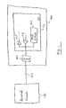
- FIG. 1 shows a circuit arrangement that includes an ESD circuit according to an exemplary embodiment of the invention.
- FIG. 2 illustrates a circuit arrangement that includes PLD 103 with ESD protection according to the invention.
- FIG. 3 depicts exemplary waveforms relating to ESD mode operation of an ESD circuit according to the invention.
- FIG. 4 shows an exemplary waveform pertaining to the hot-socket mode operation of an ESD circuit according to the invention.
- FIG. 5 illustrates exemplary waveforms relating to the steady-state mode operation of an ESD circuit according to the invention.
- FIG. 6 depicts a circuit arrangement for an ESD circuit according to an exemplary embodiment of the invention.
- FIG. 7 shows a partial layout for an ESD circuit according to an exemplary embodiment of the invention.
- the inventive concepts contemplate ESD circuits for use in a wide variety of ICs, such as programmable logic devices (PLDs).
- the ESD circuits protect the IC against potential damage by ESD events.
- the ESD circuits can support hot-socket operation, as desired.
- the inventive ESD circuits provides several advantages, as the description in this document makes apparent to persons of ordinary skill in the art. First, it provides a trigger for the ballasted ESD transistor, thus allowing relatively precise control of snap-back voltage. Second, it provides for snap-back voltage engineering with little or no impact to the ballast device characteristics. Third, it minimizes impact to the I/O performance by minimizing capacitance in the I/O path. The ESD circuit also meets hot-socket and ESD specifications simultaneously, thus providing a high-performance I/O solution.
- FIG. 1 shows a circuit arrangement that includes ESD circuit according to an exemplary embodiment of the invention.
- the circuit arrangement includes IC 100 coupled to an external circuit 150 via pad 163 of IC 100 , and a coupling mechanism 153 .
- Coupling mechanism 153 may constitute a wire, printed circuit board traces, conductors, etc.
- I/O circuitry 112 provides a mechanism for circuits within IC 100 to communicate with external circuit 153 , as persons of ordinary skill in the art who have the benefit of the description of the invention understand.
- I/O circuitry 112 includes driver 157 , receiver 155 , and ESD circuit 160 .
- Driver 157 couples to desired circuits within IC 100 , and communicates information to external circuit 150 via pad 163 and coupling mechanism 153 .
- Receiver 153 performs the inverse function. In other words, it receives information from external circuit 150 via coupling mechanism 153 and pad 163 , and provides the information to desired circuits within IC 100 .
- ESD circuit 160 couples to pad 163 .
- ESD circuit 160 acts to clamp the voltage at pad 163 and, thus, protect the circuitry within IC 100 from damage or degradation.
- ESD circuit 160 can protect IC 100 even in the absence of external circuit 150 and coupling mechanism 153 .
- static electricity conducted through the fingers or hand of a person touching pad 163 , may expose IC 100 to an ESD event.
- ESD 160 clamps the ESD voltage at pad 160 to protect IC 100 .
- FIG. 1 shows a simplified or general block diagram.
- ESD circuit 160 may be used to perform the function of driver 157 , as desired (see FIG. 6 for an example).
- FIG. 2 shows a circuit arrangement that includes PLD 103 with ESD protection according to the invention (PLD 103 constitutes a special case of IC 100 ).
- PLD 103 includes configuration circuitry 130 , configuration memory (CRAM) 133 , control circuitry 136 , programmable logic 106 , programmable interconnect 109 , and I/O circuitry 112 .
- PLD 103 may include test/debug circuitry 115 , one or more processors 118 , one or more communication circuitry 121 , one or more memories 124 , one or more controllers 127 , as desired.
- Programmable logic 106 includes blocks of configurable or programmable logic circuitry, such as look-up tables (LUTs), product-term logic, multiplexers (MUXs), logic gates, registers, memory, and the like.
- Programmable interconnect 109 couples to programmable logic 106 and to other blocks and circuitry within PLD 103 , as desired. As described below in detail, programmable interconnect 109 provides configurable interconnects (coupling mechanisms) between various blocks within programmable logic 106 and other circuitry within or outside PLD 103 .
- Control circuitry 136 controls various operations within PLD 103 .
- PLD configuration circuitry 130 uses configuration data (which it obtains from an external source, such as a storage device, a host, etc.) to program or configure the functionality of PLD 103 .
- Configuration data are typically used to store information in CRAM 133 .
- the contents of CRAM 133 determine the functionality of various blocks of PLD 103 , such as programmable logic 106 and programmable interconnect 109 .
- Test/debug circuitry 115 facilitates the testing and troubleshooting of various blocks and circuits within PLD 103 .
- Test/debug circuitry 115 may include a variety of blocks or circuits known to persons of ordinary skill in the art who have the benefit of the description of the invention.
- test/debug circuitry 115 may include circuits for performing tests after PLD 103 powers up or resets, as desired.
- Test/debug circuitry 115 may also include coding and parity circuits, as desired.
- PLD 103 may include one or more processors 118 .
- Processor 118 may couple to other blocks and circuits within PLD 103 .
- Processor 118 may receive data and information from circuits within or external to PLD 103 and process the information in a wide variety of ways, as persons skilled in the art with the benefit of the description of the invention appreciate.
- One or more of processor(s) 118 may constitute a digital signal processor (DSP).
- DSPs allow performing a wide variety of signal processing tasks, such as compression, decompression, audio processing, video processing, filtering, and the like, as desired.
- DSPs allow performing a wide variety of signal processing tasks, such as compression, decompression, audio processing, video processing, filtering, and the like, as desired.
- DSP digital signal processor
- PLD 103 may also include one or more communication circuits 121 .
- Communication circuit(s) 121 may facilitate data and information exchange between various circuits within PLD 103 and circuits external to PLD 103 , as persons of ordinary skill in the art who have the benefit of the description of the invention understand.
- PLD 103 may further include one or more memories 124 and one or more controller(s) 127 .
- Memory 124 allows the storage of various data and information (such as user-data, intermediate results, calculation results, etc.) within PLD 103 .
- Memory 124 may have a granular or block form, as desired.
- Controller 127 allows interfacing to, and controlling the operation and various functions of circuitry outside the PLD.
- controller 127 may constitute a memory controller that interfaces to and controls an external synchronous dynamic random access memory (SDRAM), as desired.
- SDRAM synchronous dynamic random access memory
- FIG. 1 shows a simplified block diagram of PLD 103 .
- PLD 103 may include other blocks and circuitry, as persons of ordinary skill in the art understand. Examples of such circuitry include clock generation and distribution circuits, redundancy circuits, and the like. Furthermore, PLD 103 may include, analog circuitry, other digital circuitry, and/or mixed-mode circuitry, as desired.
- I/O circuitry 112 includes ESD circuit 160 for protecting various circuitry within PLD 103 . More specifically, I/O circuitry 112 includes ESD circuit 160 , which couples to PLD pad 163 and, optionally, to external circuit 150 via coupling mechanism 153 . ESD circuit 160 can protect PLD 103 either “in-circuit” (e.g., coupled to external circuit 150 ), or stand-alone (e.g., not part of a circuit, but still exposed to ESD events, for example, by static electricity).
- in-circuit e.g., coupled to external circuit 150
- stand-alone e.g., not part of a circuit, but still exposed to ESD events, for example, by static electricity.
- I/O circuitry 112 may constitute a wide variety of I/O devices or circuits for performing input/output functions, as persons of ordinary skill in the art who have the benefit of the description of the invention understand. I/O circuitry 112 provides a mechanism and circuitry for various blocks within PLD 103 to communicate with external circuitry or devices, for example driver and receiver circuits (see FIG. 1 ), as desired.
- ESD circuit 160 has three modes of operation: ESD mode, hot-socket mode, and steady-state (normal operation) mode. The following description provides details of each mode.
- FIG. 3 shows exemplary waveforms relating to ESD mode operation of the ESD circuit according to the invention.
- IC 100 experiences a relatively large voltage at pad 163 .
- FIG. 3 shows a waveform of that voltage, v ESD .
- the voltage can have large peak values that may destroy or degrade circuitry within IC 100 .
- ESD circuit 160 By virtue of the protection that ESD circuit 160 affords, however, IC 100 experiences a clamped voltage (see waveform v CLAMP in FIG. 3 ) at pad 163 . In other words, during this mode, when the pad voltage rises above a given value, ESD circuit clamps the voltage at v CLAMP . Thus, ESD circuit 160 prevent exposure of other circuitry within IC 100 to the harmful, large peak of v CLAMP .
- IC 100 experiences an application of power in an unpredictable manner. More specifically, the user may apply supply voltage(s) to IC 100 with an uncertain or unknown timing. For example, one does not know in advance whether one supply voltage is applied before another supply voltage, or vice-versa.
- ESD circuit 160 has the capability of operating in this mode. To summarize, in the hot-socket mode, ESD circuit 160 can handle and accommodate random powering up of ground and supply voltages.
- pin 163 experiences voltages that correspond to information exchanged between IC 100 and external circuit 150 (e.g., logic signals).
- FIG. 5 shows example waveforms corresponding to such signals. More specifically, the voltage during steady-state operation, v ss , may have values V L (corresponding to a low logic state), V H (corresponding to a high logic state), or high-impedance state.
- Various circuitry within IC 100 for example, driver 157 or receiver 155 , may generate or accept v ss .
- FIG. 6 shows a circuit arrangement for ESD circuit 160 according to an exemplary embodiment of the invention.
- the circuit arrangement includes transistor 203 , transistor 206 , resistor 209 , capacitor 215 , and hot socket ground circuit 212 .
- the circuit may include driver 157 , as desired, in order to support providing information to circuitry external to ESD circuit 160 via pad 163 .
- Transistor 206 serves as a bias device.
- Transistor 203 includes ballast transistor or ballasted device 203 A and triggering device or transistor 203 B.
- Transistor 203 includes a multiple-finger structure, as persons of ordinary skill in the art who have the benefit of the description of the invention understand.
- Transistor 203 A may include a number of transistors in the multiple-finger structure.
- Transistor 203 B may constitute one of the transistors in the multiple-finger structure (one finger). As FIG. 6 illustrates, although they are part of the same finger structure, transistors 203 A and 203 B have separate gate drives.
- Transistors 203 A and 203 B may have a desired size that depends on factors such as design and performance specifications, the fabrication technology used, implementation details, etc.
- transistor 203 A may be 320 microns wide
- transistor 203 B may have a width of 5 microns.
- the relatively small size of transistor 203 B tends to reduce or minimize the capacitance that it presents to the I/O path (i.e., pad 163 ), thus providing relatively high I/O performance.
- the finger structure may use a suitable material, such as polysilicon, as persons of ordinary skill in the art who have the benefit of the description of the invention understand.
- a suitable material such as polysilicon
- the circuit has three modes of operation, steady-state, ESD, and hot-socket.
- steady-state normal
- the gate of transistor 206 is coupled to the supply voltage, which turns ON transistor 206 .
- Current conduction in transistor 206 grounds the gate of transistor 203 B, effectively turning it OFF. Because no or little current flows through transistor 203 B, the body of transistor 203 A has the same potential (ground) as its source (i.e., no or little voltage drop across resistor 209 ).
- transistor 203 B does not impact the operation of transistor 203 A.
- host-socket ground circuit 212 has no impact on transistor 203 A (i.e., does not bias its gate).
- driver 157 (or other suitable circuit) can drive the gate of transistor 203 A and, hence, pad 163 .
- transistor 203 A By supplying appropriate voltages to the gate of transistor 203 A, one can drive pad 163 with logic low and logic high signals and therefore communicate information to circuits outside IC 100 . Conversely, by turning OFF transistor 203 A, one may receive information from outside IC 100 via pad 163 (i.e., allow external circuitry provide the information by driving pad 163 ).
- Capacitor 215 has a relatively large capacitance compared to that parasitic capacitance.
- transistor 203 B serves as a driver transistor during steady-state operation, which may make some of its characteristics subject to I/O performance specifications.
- Transistor 203 B serves as the trigger device for transistor 203 A.
- By controlling the relative values of the device capacitances of transistor 203 B and the capacitance of capacitor 209 one may design a desired trigger point without impacting the I/O performance of transistor 203 A.
- Capacitor 215 acts momentarily as a short circuit, and drives the gate of transistor 203 B hard (i.e., rapidly raises the gate voltage).
- an elevated gate voltage facilitates snap back of transistor 203 B.
- the ESD event causes transistor 203 B to snap back and conduct current.
- transistor 203 B Current flow through transistor 203 B results in a voltage drop across resistor 209 .
- the voltage drop acts as a finite body-source voltage of transistor 203 A, thus altering its threshold voltage.
- the threshold voltage, V T of transistor 203 A depends on a number of factors, such as the voltage between its source and body.
- the following equation provides the threshold voltage as a function of the body-to-source voltage:
- V T V T ⁇ ( 0 ) + ⁇ ⁇ ⁇ 2 ⁇ ⁇ F - v BS - 2 ⁇ ⁇ F ⁇ . ( 1 )
- Equation 1 one may write Equation 1 in terms of the source-to-body voltage:
- V T V T ⁇ ( 0 ) + ⁇ ⁇ ⁇ 2 ⁇ ⁇ F - v SB - 2 ⁇ ⁇ F ⁇ , ( 2 )
- the threshold voltage, V T equals V T(o) .
- Equation 2 shows, for a finite body factor, ⁇ , the transistor's threshold voltage increases as the source-to-body voltage, v SB , increases. Thus, raising the body voltage of transistor 203 A and, hence, its body-to-source voltage, results in a decreased threshold voltage.
- the decreased threshold voltage helps transistor 203 A to snap back.
- one finger in the multiple-finger structure snaps back first, and other fingers follow, resulting in snap back of the entire structure.
- transistor 203 A snaps back (as a result of the snap-back of transistor 203 B), it couples pad 163 to ground, thus shunting and discharging the ESD energy and protecting IC 100 .
- hot-socket ground circuit 212 couples the gate of transistor 203 A to ground. As a result, transistor 203 A turns OFF.
- the voltage applied to pad 163 increases as a function of time. In the absence of an ESD event, however, the voltage does not rise sufficiently to turn ON transistor 203 B hard. Rather, transistor 203 B either remains OFF or turns ON slightly, and leaks a limited amount of current to ground.
- transistor 203 B If the voltage at pad 163 rises beyond the threshold voltage of transistor 203 B (or rises too rapidly, similar to an ESD event), transistor 203 B will turn ON, and shunt pad 163 to ground through resistor 209 . Thus, in this mode, transistor 203 B allows the voltage at pad 163 to rise in a controlled manner.
- Table 1 below provides a summary of the state of transistors 203 A, 203 B, and 206 during the three modes of operation:
- FIG. 7 shows a partial layout of an ESD circuit according to an illustrative embodiment of the invention.
- the layout includes area 303 , which houses transistor 203 B (see FIG. 6 ), and area 306 , which houses transistor 203 A.
- Area 309 denotes a p-tap to the p-well of transistor 203 A, as persons of ordinary skill in the art who have the benefit of the description of the invention understand.
- the layout in FIG. 7 places transistor 203 B strategically so as to facilitate snap-back of transistor 203 A during an ESD event. More specifically, area 303 is centered or substantially centered with respect to area 306 . The placement of the two areas provides a relatively uniform turning ON or snapping back of transistor 203 B.
- NMOS transistors As an example, persons of ordinary skill in the art who have the benefit of the description of the invention understand that one may apply the concepts to other technologies. For example, rather than using NMOS transistors, one may use PMOS transistors, or a combination (i.e., complementary metal oxide semiconductor, or CMOS), as desired.
- CMOS complementary metal oxide semiconductor
- Such circuitry includes, for example, devices known as complex programmable logic device (CPLD), programmable gate array (PGA), structured application specific ICs (structured ASICs), and field programmable gate array (FPGA).
- CPLD complex programmable logic device
- PGA programmable gate array
- structured ASICs structured application specific ICs
- FPGA field programmable gate array
- circuit implementation may or may not contain separately identifiable hardware for the various functional blocks and may or may not use the particular circuitry shown.
- the choice of circuit implementation depends on various factors, such as particular design and performance specifications for a given implementation, as persons of ordinary skill in the art who have the benefit of the description of the invention understand.
- Other modifications and alternative embodiments of the invention in addition to those described here will be apparent to persons of ordinary skill in the art who have the benefit of the description of the invention. Accordingly, this description teaches those skilled in the art the manner of carrying out the invention and are to be construed as illustrative only.
Landscapes
- Engineering & Computer Science (AREA)
- Power Engineering (AREA)
- Physics & Mathematics (AREA)
- Condensed Matter Physics & Semiconductors (AREA)
- General Physics & Mathematics (AREA)
- Computer Hardware Design (AREA)
- Microelectronics & Electronic Packaging (AREA)
- Semiconductor Integrated Circuits (AREA)
Abstract
Description
Alternatively, one may write Equation 1 in terms of the source-to-body voltage:
where
-
- VT(o)=the threshold voltage with the source-to-body voltage (or body-to-source voltage) set to zero;
- γ=the body factor, a constant that depends on the doping levels of the body;
- φF=a constant;
- vBS=the total body-to-source voltage (i.e., including AC and DC components); and
- vSB=the total source-to-body voltage (i.e., including AC and DC components).
| TABLE 1 | |||
| MODE OF | TRANSISTOR | | |
| |
203A | ||
| 203B | |||
| 206 | |||
| Steady-State | Depends on gate | OFF | ON |
| voltage | |||
| ESD | Snap back | Snap back | OFF |
| Hot-socket | OFF | Slightly ON | OFF |
Claims (10)
Priority Applications (1)
| Application Number | Priority Date | Filing Date | Title |
|---|---|---|---|
| US11/211,060 US8089744B1 (en) | 2005-08-24 | 2005-08-24 | Apparatus and methods for electrostatic discharge circuitry with snap-back device |
Applications Claiming Priority (1)
| Application Number | Priority Date | Filing Date | Title |
|---|---|---|---|
| US11/211,060 US8089744B1 (en) | 2005-08-24 | 2005-08-24 | Apparatus and methods for electrostatic discharge circuitry with snap-back device |
Publications (1)
| Publication Number | Publication Date |
|---|---|
| US8089744B1 true US8089744B1 (en) | 2012-01-03 |
Family
ID=45374608
Family Applications (1)
| Application Number | Title | Priority Date | Filing Date |
|---|---|---|---|
| US11/211,060 Expired - Fee Related US8089744B1 (en) | 2005-08-24 | 2005-08-24 | Apparatus and methods for electrostatic discharge circuitry with snap-back device |
Country Status (1)
| Country | Link |
|---|---|
| US (1) | US8089744B1 (en) |
Cited By (2)
| Publication number | Priority date | Publication date | Assignee | Title |
|---|---|---|---|---|
| US20140107961A1 (en) * | 2012-10-11 | 2014-04-17 | Industrial Technology Research Institute | Testing method and testing system for semiconductor element |
| US10191108B2 (en) | 2015-11-19 | 2019-01-29 | Globalfoundries Inc. | On-chip sensor for monitoring active circuits on integrated circuit (IC) chips |
Citations (8)
| Publication number | Priority date | Publication date | Assignee | Title |
|---|---|---|---|---|
| US5701024A (en) * | 1995-10-05 | 1997-12-23 | Cypress Semiconductor Corp. | Electrostatic discharge (ESD) protection structure for high voltage pins |
| US6335636B1 (en) * | 1998-09-09 | 2002-01-01 | Altera Corporation | Programmable logic device input/output circuit configurable as reference voltage input circuit |
| US6583972B2 (en) | 2000-06-15 | 2003-06-24 | Sarnoff Corporation | Multi-finger current ballasting ESD protection circuit and interleaved ballasting for ESD-sensitive circuits |
| US6646840B1 (en) * | 2000-08-03 | 2003-11-11 | Fairchild Semiconductor Corporation | Internally triggered electrostatic device clamp with stand-off voltage |
| US20040160717A1 (en) * | 2003-02-13 | 2004-08-19 | May James T. | Destructive electrical transient protection |
| US6898062B2 (en) * | 2001-07-05 | 2005-05-24 | Sarnoff Corporation | Electrostatic discharge (ESD) protection device with simultaneous and distributed self-biasing for multi-finger turn-on |
| US6939752B1 (en) * | 2003-08-22 | 2005-09-06 | Altera Corporation | Apparatus and methods for integrated circuit with devices with body contact and devices with electrostatic discharge protection |
| US20050253626A1 (en) * | 2000-08-22 | 2005-11-17 | Yan Chong | Supply voltage detection circuit |
-
2005
- 2005-08-24 US US11/211,060 patent/US8089744B1/en not_active Expired - Fee Related
Patent Citations (9)
| Publication number | Priority date | Publication date | Assignee | Title |
|---|---|---|---|---|
| US5701024A (en) * | 1995-10-05 | 1997-12-23 | Cypress Semiconductor Corp. | Electrostatic discharge (ESD) protection structure for high voltage pins |
| US6335636B1 (en) * | 1998-09-09 | 2002-01-01 | Altera Corporation | Programmable logic device input/output circuit configurable as reference voltage input circuit |
| US6583972B2 (en) | 2000-06-15 | 2003-06-24 | Sarnoff Corporation | Multi-finger current ballasting ESD protection circuit and interleaved ballasting for ESD-sensitive circuits |
| US6646840B1 (en) * | 2000-08-03 | 2003-11-11 | Fairchild Semiconductor Corporation | Internally triggered electrostatic device clamp with stand-off voltage |
| US20050253626A1 (en) * | 2000-08-22 | 2005-11-17 | Yan Chong | Supply voltage detection circuit |
| US6898062B2 (en) * | 2001-07-05 | 2005-05-24 | Sarnoff Corporation | Electrostatic discharge (ESD) protection device with simultaneous and distributed self-biasing for multi-finger turn-on |
| US20050180073A1 (en) * | 2001-07-05 | 2005-08-18 | John Armer | Electrostatic discharge (ESD) protection device with simultaneous and distributed self-biasing for multi-finger turn-on |
| US20040160717A1 (en) * | 2003-02-13 | 2004-08-19 | May James T. | Destructive electrical transient protection |
| US6939752B1 (en) * | 2003-08-22 | 2005-09-06 | Altera Corporation | Apparatus and methods for integrated circuit with devices with body contact and devices with electrostatic discharge protection |
Cited By (3)
| Publication number | Priority date | Publication date | Assignee | Title |
|---|---|---|---|---|
| US20140107961A1 (en) * | 2012-10-11 | 2014-04-17 | Industrial Technology Research Institute | Testing method and testing system for semiconductor element |
| US9726713B2 (en) * | 2012-10-11 | 2017-08-08 | Industrial Technology Research Institute | Testing method and testing system for semiconductor element |
| US10191108B2 (en) | 2015-11-19 | 2019-01-29 | Globalfoundries Inc. | On-chip sensor for monitoring active circuits on integrated circuit (IC) chips |
Similar Documents
| Publication | Publication Date | Title |
|---|---|---|
| US7274546B2 (en) | Apparatus and method for improved triggering and leakage current control of ESD clamping devices | |
| Meng et al. | Novel decoupling capacitor designs for sub-90nm CMOS technology | |
| US7098511B2 (en) | ESD protection circuit | |
| JP3773506B2 (en) | Semiconductor integrated circuit device | |
| US7742265B2 (en) | High voltage power supply clamp circuitry for electrostatic discharge (ESD) protection | |
| US20090268359A1 (en) | Electrostatic discharge power clamp with improved electrical overstress robustness | |
| JPH0855965A (en) | Integrated circuit including overvoltage protection mechanism and protecting method therefor | |
| US6927957B1 (en) | Electrostatic discharge clamp | |
| US20050030688A1 (en) | ESD protection circuit having a control circuit | |
| JP3691554B2 (en) | Protection circuit for ESD protection | |
| US7889469B2 (en) | Electrostatic discharge protection circuit for protecting semiconductor device | |
| TW201029142A (en) | Method and apparatus to reduce footprint of ESD protection within an integrated circuit | |
| JP2005064374A (en) | Semiconductor integrated circuit device | |
| JP2011071502A (en) | Method for designing integrated electronic circuit having esd protection and circuit obtained thereof | |
| US20060268477A1 (en) | Apparatus for ESD protection | |
| US7079369B2 (en) | Active power/ground ESD trigger | |
| KR101128897B1 (en) | Semiconductor device | |
| US20060198069A1 (en) | Power ESD clamp protection circuit | |
| US8089744B1 (en) | Apparatus and methods for electrostatic discharge circuitry with snap-back device | |
| US20090295470A1 (en) | Fast turn on active dcap cell | |
| US6643109B1 (en) | Fully synthesisable and highly area efficient very large scale integration (VLSI) electrostatic discharge (ESD) protection circuit | |
| WO1999065079A1 (en) | A method of programmability and an architecture for cold sparing of cmos arrays | |
| WO2004068543A2 (en) | Electrostatic discharge circuit and method therefor | |
| JP3780896B2 (en) | Semiconductor integrated circuit device | |
| TW202406262A (en) | Esd protection circuit and operating method thereof |
Legal Events
| Date | Code | Title | Description |
|---|---|---|---|
| AS | Assignment |
Owner name: ALTERA CORPORATION, CALIFORNIA Free format text: ASSIGNMENT OF ASSIGNORS INTEREST;ASSIGNORS:RAHIM, IFRAN;HUANG, CHENG HSIUNG;LIU, YOW-JUANG BILL;AND OTHERS;SIGNING DATES FROM 20050816 TO 20050822;REEL/FRAME:016921/0724 |
|
| ZAAA | Notice of allowance and fees due |
Free format text: ORIGINAL CODE: NOA |
|
| ZAAB | Notice of allowance mailed |
Free format text: ORIGINAL CODE: MN/=. |
|
| STCF | Information on status: patent grant |
Free format text: PATENTED CASE |
|
| FPAY | Fee payment |
Year of fee payment: 4 |
|
| MAFP | Maintenance fee payment |
Free format text: PAYMENT OF MAINTENANCE FEE, 8TH YEAR, LARGE ENTITY (ORIGINAL EVENT CODE: M1552); ENTITY STATUS OF PATENT OWNER: LARGE ENTITY Year of fee payment: 8 |
|
| FEPP | Fee payment procedure |
Free format text: MAINTENANCE FEE REMINDER MAILED (ORIGINAL EVENT CODE: REM.); ENTITY STATUS OF PATENT OWNER: LARGE ENTITY |
|
| LAPS | Lapse for failure to pay maintenance fees |
Free format text: PATENT EXPIRED FOR FAILURE TO PAY MAINTENANCE FEES (ORIGINAL EVENT CODE: EXP.); ENTITY STATUS OF PATENT OWNER: LARGE ENTITY |
|
| STCH | Information on status: patent discontinuation |
Free format text: PATENT EXPIRED DUE TO NONPAYMENT OF MAINTENANCE FEES UNDER 37 CFR 1.362 |
|
| FP | Lapsed due to failure to pay maintenance fee |
Effective date: 20240103 |