WO2018123550A1 - ガスフロースパッタリング装置及びスパッタリングターゲット原料の製造方法 - Google Patents
ガスフロースパッタリング装置及びスパッタリングターゲット原料の製造方法 Download PDFInfo
- Publication number
- WO2018123550A1 WO2018123550A1 PCT/JP2017/044448 JP2017044448W WO2018123550A1 WO 2018123550 A1 WO2018123550 A1 WO 2018123550A1 JP 2017044448 W JP2017044448 W JP 2017044448W WO 2018123550 A1 WO2018123550 A1 WO 2018123550A1
- Authority
- WO
- WIPO (PCT)
- Prior art keywords
- sputtering
- target
- gas flow
- targets
- pair
- Prior art date
- Legal status (The legal status is an assumption and is not a legal conclusion. Google has not performed a legal analysis and makes no representation as to the accuracy of the status listed.)
- Ceased
Links
Images


Classifications
-
- C—CHEMISTRY; METALLURGY
- C23—COATING METALLIC MATERIAL; COATING MATERIAL WITH METALLIC MATERIAL; CHEMICAL SURFACE TREATMENT; DIFFUSION TREATMENT OF METALLIC MATERIAL; COATING BY VACUUM EVAPORATION, BY SPUTTERING, BY ION IMPLANTATION OR BY CHEMICAL VAPOUR DEPOSITION, IN GENERAL; INHIBITING CORROSION OF METALLIC MATERIAL OR INCRUSTATION IN GENERAL
- C23C—COATING METALLIC MATERIAL; COATING MATERIAL WITH METALLIC MATERIAL; SURFACE TREATMENT OF METALLIC MATERIAL BY DIFFUSION INTO THE SURFACE, BY CHEMICAL CONVERSION OR SUBSTITUTION; COATING BY VACUUM EVAPORATION, BY SPUTTERING, BY ION IMPLANTATION OR BY CHEMICAL VAPOUR DEPOSITION, IN GENERAL
- C23C14/00—Coating by vacuum evaporation, by sputtering or by ion implantation of the coating forming material
- C23C14/22—Coating by vacuum evaporation, by sputtering or by ion implantation of the coating forming material characterised by the process of coating
- C23C14/34—Sputtering
-
- G—PHYSICS
- G11—INFORMATION STORAGE
- G11B—INFORMATION STORAGE BASED ON RELATIVE MOVEMENT BETWEEN RECORD CARRIER AND TRANSDUCER
- G11B5/00—Recording by magnetisation or demagnetisation of a record carrier; Reproducing by magnetic means; Record carriers therefor
- G11B5/84—Processes or apparatus specially adapted for manufacturing record carriers
- G11B5/851—Coating a support with a magnetic layer by sputtering
Definitions
- the present invention relates to a gas flow sputtering apparatus and a method for producing a sputtering target material.
- a material based on Co, Fe, or Ni which is a ferromagnetic metal, is used as a magnetic thin film material for recording.
- a Co—Cr-based or Co—Cr—Pt-based ferromagnetic alloy containing Co as a main component has been used for a recording layer of a hard disk employing an in-plane magnetic recording method.
- nonmagnetic particles such as oxide and carbon are dispersed in a Co—Cr—Pt ferromagnetic alloy containing Co as a main component.
- Many composite materials are used.
- a magnetic thin film of a magnetic recording medium such as a hard disk is often produced by sputtering a sputtering target containing the above materials as a component because of its high productivity.
- the contained non-magnetic particles cause abnormal discharge during sputtering, and particles are generated due to this abnormal discharge.
- the sputtering target is generally manufactured by a powder sintering method.
- a powder sintering method In order to reduce particles, it is known that miniaturization of nonmagnetic particles in a sputtering target is very effective. For this purpose, it is an effective technique to mechanically pulverize and mix the raw material powders using a powerful ball mill or the like.
- a powerful ball mill or the like For this purpose, there is a physical limit to the refinement of the structure, and it has been difficult to completely eliminate the generation of particles.
- the oxide be refined by using a PVD or CVD method instead of the conventional mechanical pulverization and mixing.
- a method is described in which a magnetic material is formed on a substrate by PVD or CVD, the substrate is removed from the formed magnetic material, and this is pulverized into a raw material.
- the average particle diameter of the oxide in the sputtering target can be reduced to 400 nm or less.
- a target material is formed using a DC magnetron sputtering apparatus.
- a gas flow sputtering method is also known (eg, Japanese Patent Application Laid-Open No. 2006-130378, Japanese Patent Application Laid-Open No. 2007-186771, Japanese Patent Application Laid-Open No. 2008-1957).
- the gas flow sputtering method is a method in which sputtering is performed under a relatively high pressure, and sputtered particles are transported to a deposition target substrate by a forced flow of gas and deposited. Since this gas flow sputtering method does not require high vacuum evacuation, it is possible to form a film by mechanical pump evacuation without using a large evacuation device like the conventional normal sputtering method, and it is inexpensive. It can be implemented with simple equipment.
- the gas flow sputtering method can form a film 10 to 1000 times faster than the normal sputtering method. Therefore, according to the gas flow sputtering method, the film formation cost can be reduced by reducing the equipment cost and the film formation time.
- the invention described in International Publication No. 2013/13662 is an effective technique for refining the structure of a non-magnetic material particle-dispersed sputtering target.
- PVD or CVD is used on the substrate. It is necessary to carry out a film forming step.
- a film is formed using a high-performance apparatus such as a DC magnetron sputtering apparatus, there is a problem that the manufacturing cost of the sputtering target increases, and there is a problem that productivity is low.
- the gas flow sputtering method can form a film at a high speed and the equipment cost is low. Therefore, it is considered advantageous if the raw material of the sputtering target can be manufactured by using the gas flow sputtering method.
- Patent Documents 2 to 4 disclose gas polymer sputtering fuel cell electrode catalyst layers, dye-sensitized solar cell semiconductor electrode layers, photocatalyst films, antireflection films, electrochromic elements, transparent conductive films. Remains to be described.
- the apparatus improvement from the viewpoint of manufacturing the raw material of a sputtering target industrially is not made.
- a large amount of raw material is required. Therefore, it is necessary to perform continuous sputtering stably for a long time, and there is still room for improvement from the viewpoint of the apparatus configuration and manufacturing method therefor. Has been.
- the present invention was created in view of the above circumstances, and one object of the present invention is to provide a gas flow sputtering apparatus suitable for producing a sputtering target material stably for a long time at a high sputtering rate. To do. Another object of the present invention is to provide a target for gas flow sputtering. Another object of the present invention is to provide a method for producing a sputtering target material using the gas flow sputtering apparatus.
- the present inventors have found that the film thickness uniformity and surface properties of the sputtered film formed by the gas flow sputtering apparatus are almost a problem for the purpose of producing the raw material of the sputtering target. Not. For this purpose, it is more important to suppress abnormal discharge at a high sputtering rate than to improve the quality of the sputtered film. Based on this viewpoint, the present inventor has found that a gas flow sputtering apparatus having the following configuration using a flat plate facing target is effective.
- An apparatus a conductive fixing member for fixing each flat plate target to a cooling device, one or more gas discharge ports for supplying sputtering gas between the pair of flat plate targets, and a pair of flat plates
- a gas flow sputtering apparatus comprising a member for depositing sputter particles arranged to face the gas discharge port on the opposite side of the gas discharge port across the space between the targets,
- the pair of flat targets have attachment portions extending from the respective side surfaces, and the pair of flat targets are fixed to the cooling device in a positional relationship where the attachment portions are sandwiched between the fixing member and the cooling device.
- the fixing member is covered with an insulating shield member that does not contact the pair of flat targets. It is a gas flow sputtering apparatus.
- the pair of flat targets are conductive.
- the pair of flat targets are fixed by the fixing member in a state where a surface opposite to the sputtering surface is in direct or indirect contact with the cooling device. ing.
- the closest approach distance between each flat plate target and the insulating shield member is adjusted to 0.1 to 5 mm.
- the insulating shield member is made of aluminum oxide, silicon oxide, zirconium oxide, magnesium oxide, yttrium oxide, calcium oxide, titanium oxide, and boron nitride. It is composed of one or more materials selected from the group.
- the insulating shield member has a peripheral wall erected so as to surround the side surface at intervals along the side surface of each flat plate target. Have.
- the distance between the side surface of each flat plate target and the peripheral wall of the insulating shield member is 0.1 to 2 mm.
- the insulating shield member is disposed so as to cover the edge of the sputtering surface of each flat plate target.
- the pair of flat plate targets is composed of a composite of a nonmagnetic material and a magnetic material.
- the present invention is a method for producing a sputtering target material including a step of sputtering using a gas flow sputtering apparatus according to the present invention.
- sputtering is performed with a power density of 10 W / cm 2 or more.
- the flow rate of the sputtering gas is expressed as a flow rate per 1 cm 2 of the total projected area of the facing sputtering surfaces of the pair of flat plate targets, and is 1 sccm / cm 2 or more.
- sputtering is performed with a sputtering gas pressure of 10 Pa or more.
- the member for depositing sputtered particles is a used sputtering target, which includes depositing sputtered particles on the eroded portion of the target.
- the total mass of sputtered particles deposited on the insulating shield member is calculated from the mass of sputtered particles deposited on the member on which the sputtered particles are deposited. Including enlarging.
- abnormal discharge is less likely to occur when a sputtering target material is produced using a gas flow sputtering apparatus, so that it is possible to perform sputtering continuously and stably for a long time.
- This makes it possible to produce a sputtering target material, particularly a non-magnetic material particle-dispersed sputtering target material with a refined structure, at a higher production efficiency and at a lower cost than the prior art.
- FIG. 1 It is a schematic diagram which shows the 5th example of the cross-sectional structure of the target for gas flow sputtering which concerns on this invention, and a fixing member (backing plate use). An example of arrangement
- FIG. 1 shows an example of a basic structure inside a gas flow sputtering apparatus according to the present invention
- FIGS. 2-1 to 2-3 show schematic apparatus configuration examples of the gas flow sputtering apparatus according to the present invention.
- the pair of flat targets 10a and 10b can increase the plasma density uniformly on the target surface without exhibiting unexpected behavior when the sputtering surfaces are arranged in parallel with each other. From the viewpoint that it is effective in improving the erosion speed. However, it is also possible to perform sputtering while tilting the sputter surfaces of each other rather than in parallel.
- a negative voltage is applied to each of the targets 10a and 10b to generate a plasma of a sputtering gas 17 such as Ar in the space 12 between the pair of flat targets 10a and 10b. Is generated.
- FIGS. 2-1 to 2-3 show exemplary potentials of each device during sputtering.
- the pair of flat targets 10a and 10b are required to have a cathode potential at the time of sputtering, but there is no particular limitation on the potential of other portions as long as the sputtering apparatus can be operated safely, but from the viewpoint of stable operation. Since there exists a suitable aspect, it is mentioned later.
- the outer wall of the sputtering chamber 11 is set to an anode potential from the viewpoint of safety.
- an insulating member is effective when it is necessary to insulate between the anode potential portion and the cathode potential portion except for a space.
- the power source of the gas flow sputtering apparatus may be either a DC power supply or an AC power supply, but the DC power supply 15 is preferable because the cost of the power supply apparatus is low and the sputtering rate per unit time is fast.
- the generated sputtered particles 13 flow from the sputter gas discharge port 14, ride on the forced gas flow of the sputter gas 17 flowing in the direction of the arrow through the space 12 between the pair of flat plate targets 10a, 10b, and the pair of flat plate targets 10a. 10b, a member 16 for depositing sputtered particles 13 disposed so as to face the sputter gas discharge port 14 outside the space 12 between 10b (the space surrounded by the one-dot chain line in FIGS. 2-1 to 2-3).
- the space between a pair of flat plate targets is formed by extending the outline of the sputtering surface of one flat plate target in a direction normal to the sputtering surface and approaching the other flat plate target.
- the space surrounded by the figure and the space surrounded by the figure formed by extending the outline of the sputtering surface of the other flat plate target in the direction normal to the sputtering surface and approaching the flat plate target The point where both overlap.
- the member on which sputter particles are deposited faces the sputter gas discharge port means that at least one sputter gas discharge port has a straight line extending in the gas discharge direction and a surface on which the sputter particles are deposited. It means having an intersection.
- the member 16 for depositing the sputtered particles 13 can be supported by a holder 18.
- the holder 18 is installed on the opposite side of the sputtering gas discharge port 14 through the space 12 sandwiched between the pair of flat targets 10a and 10b. Thereafter, the sputtering gas 17 is discharged from the exhaust port 20.
- the exhaust port 20 can be installed, for example, behind the holder 18 (in other words, the back side). By installing the exhaust port 20 behind the holder 18, the sputter particles 13 accompanying the sputter gas 17 can be efficiently collided with the member 16.
- the distance between the pair of flat targets 10a and 10b before the start of sputtering is preferably 100 mm or less, more preferably 50 mm or less, still more preferably 45 mm or less, and 40 mm or less. Even more preferably.
- the distance (S 1 ) between the pair of flat targets 10a and 10b is too short, the amount of gas that carries the sputtered particles 13 decreases and the sputtered particles 13 reattach to the target surface. It becomes difficult to deposit efficiently on the member 16 to be deposited.
- the spacing between 10b and (S 1) is raised the flow rate of sputtering gas passing therebetween, is also conceivable to not to adhere the sputtered particles 13 to the opposing target surface In this case, however, a large amount of sputtering gas and a vacuum pump with a large exhaust capacity are required.
- the distance between the pair of flat targets 10a and 10b before the start of sputtering is preferably 10 mm or more, and more preferably 15 mm or more.
- the thickness of the target becomes thinner due to erosion as the sputtering time becomes longer. For this reason, the distance between the pair of flat targets 10a and 10b increases in conjunction with the sputtering time unless any allowance is provided, and the voltage applied to the target gradually increases, increasing the risk of causing abnormal discharge. To do. However, if the distance between the pair of flat targets 10a and 10b can be maintained within a certain range regardless of the thickness of the target, for example, a suitable range of the distance between the pair of flat targets 10a and 10b described above, abnormal discharge may occur. There is no need to increase the risk of occurrence.
- the interval between the pair of flat targets can be maintained within a certain range.
- An interval adjusting mechanism 19 is provided so that a desired interval can be set at the start of sputtering.
- the pair of flat targets 10 a and 10 b are each fixed to the cooling device 50 to form an integral structural component, and each integral structural component can be moved by a corresponding interval adjusting mechanism 19.
- the interval adjusting mechanism 19 is not particularly limited, and any known mechanism may be employed, and examples thereof include a linear motion mechanism such as a cylinder linear motion mechanism and a ball screw linear motion mechanism.
- the driving method is not particularly limited, and examples thereof include motor driving, hydraulic driving, and air driving. From the viewpoint of enabling precise position adjustment, a linear motion mechanism driven by a motor is preferable.
- the interval between the pair of flat targets 10a and 10b may be changed automatically to a desired set value, or may be changed manually. Further, a change in the interval between the pair of flat targets 10a and 10b may be monitored during sputtering, and feedback control may be performed so that the initially set interval is maintained during sputtering.
- the feedback control may be manual or automatic.
- a load cell is installed so that each weight of the flat targets 10a and 10b can be measured.
- a method of calculating an average decrease amount of the target thickness that is, an average increase amount of the interval between the targets from the projected area of the sputtering surface.
- a computer may be installed in the apparatus so that the average reduction amount of the target thickness is automatically calculated, or the calculation result may be displayed on a display attached to the apparatus.
- the relationship between the discharge time and the integrated power and the average reduction amount of the target thickness is obtained in advance, and based on this, at least the average of the target thickness from the discharge time and the integrated power.
- a method of calculating the decrease amount is also conceivable.
- the interval adjusting mechanism 19 by operating the interval adjusting mechanism 19 manually or automatically so that the average interval between the targets 10a and 10b is reduced by an amount corresponding to the sum of the average reduction amounts of the thicknesses of the targets 10a and 10b, a pair is formed from the start to the end of sputtering. It is possible to keep the interval between the flat plate targets 10a and 10b within a certain range. Even if the distance between the pair of flat plate targets 10a and 10b is changed by about 1 cm, the voltage can be changed by 100 V or more. From the viewpoint of continuously performing stable sputtering, a pair of flat plates from the start of sputtering to the end of sputtering.
- the change in the average distance between the targets 10a and 10b is preferably 5 mm or less, more preferably 4 mm or less, still more preferably 3 mm or less, still more preferably 2 mm or less, and even more preferably 1 mm or less. Even more preferably.
- the spacing adjusting mechanism 19 can be installed in the sputtering chamber 11 as shown in FIG. 2B.
- the spacing adjusting mechanism 19 needs to be vacuum resistant, In the sputtering chamber 11, there is a possibility of being exposed to plasma or causing particles to accumulate and causing an operation failure.
- oil such as lubricating oil is used for the interval adjusting mechanism 19, it may evaporate in a vacuum atmosphere, and it is necessary to deal with it. Therefore, as shown in FIG. 2-3, it is preferable to install at least a part of the spacing adjusting mechanism 19 outside the sputtering chamber 11 (in FIG. 2-3, like the screw shaft in the case of the ball screw linear motion mechanism).
- the linear motion parts are installed in the chamber 11, but the power source such as a motor is installed outside the chamber 11.) As shown in FIG. 2-1, the entire distance adjusting mechanism 19 is placed outside the sputtering chamber 11. It is more preferable to install.
- the interval adjusting mechanism 19 is installed outside the sputtering chamber 11, a part of the inside of the sputtering chamber 11 has an air blocking performance that is arranged to be able to expand and contract following the operation of the interval adjusting mechanism 19. 52 is preferably delimited by the outside.
- the stretchable member 52 is not particularly limited as long as it has the above function, and examples thereof include a bellows.
- As the material of the expansion / contraction member it is preferable to use stainless steel, titanium, high nickel alloy (Hastelloy), aluminum, etc. from the viewpoint of durability in repeated expansion and contraction in a state where a force corresponding to atmospheric pressure is applied inside and outside. .
- the direction of the forced gas flow of the sputter gas 17 should be perpendicular to the surface of the member 16 on which the sputtered particles 13 are deposited. preferable.
- the material of the member 16 on which the sputtered particles 13 are deposited is not particularly limited, and plastic, glass, metal, ceramics, and the like can be used.
- the material of the member 16 on which the sputtered particles 13 are deposited is preferably a heat resistant material such as glass, metal and ceramics. This is because gas flow sputtering has an effect of flowing gas toward the member 16 side, and plasma may reach near the member 16.
- the member 16 is made of aluminum oxide, silicon oxide, zirconium oxide, magnesium oxide, yttrium oxide, calcium oxide, titanium oxide, boron nitride, aluminum, iron, copper, titanium in order to easily collect the attached sputtered particles. It is preferably composed of one or two or more materials selected from the group consisting of niobium, tantalum, tungsten, molybdenum, cobalt, chromium, nickel, and graphite, in particular, without reacting with sputtered particles, Those with poor wettability are more preferred. Further, it is preferable to select a material in consideration of contamination depending on the end use. Furthermore, the member 16 can be directly deposited on the same material as the sputtered particles 13.
- a method of regenerating the sputtering target by depositing sputtered particles on the eroded portion of the used sputtering target and returning it to the original shape is also conceivable.
- the sputtering target regenerated in this way may be pressurized and / or heated as necessary.
- the shape of the member 16 on which the sputtered particles 13 are deposited can be a plate shape or a film shape.
- the member 16 for depositing the sputtered particles 13 can be supported on the holder 18 by a method such as clamping, screwing, adhesive, adhesive tape, etc. in a gas flow sputtering apparatus. Further, the member 16 can be formed into a box-shaped container shape in order to collect more sputtered particles.
- a rare gas such as He, Ar, Ne, Kr, or Xe, or an inert gas such as N 2 or O 2 can be used alone or in combination of two or more.
- Ar is preferable from the viewpoint of cost
- Kr and Xe are preferable from the viewpoint of efficiently moving the sputtered particles.
- N 2 and / or O 2 it is also possible to use N 2 and / or O 2 as necessary.
- the flow rate of the sputtering gas can be significantly increased as compared with the DC magnetron sputtering apparatus. By increasing the flow rate of the sputtering gas, it is possible to deposit on the member that deposits the sputtered particles at high speed.
- the flow rate of the sputtering gas can be set to 1 sccm / cm 2 or more.
- the flow rate of the sputtering gas is preferably 2 sccm / cm 2 or more, and more preferably 5 sccm / cm 2 or more.
- the flow rate of the sputtering gas is too large, the pressure in the chamber rises due to the limitation of the exhaust pump capability, so it is preferably 200 sccm / cm 2 or less, preferably 100 sccm / cm 2 or less. More preferred is 50 sccm / cm 2 or less.
- sccm refers to ccm (cm 3 / min) at 0 ° C. and 1 atm.
- the flow rate is a value obtained by dividing the flow rate of the sputtering gas by the total projected area of the sputtering surfaces facing each other of the pair of flat targets 10a and 10b.
- the pressure of the sputtering gas can be significantly increased as compared with the DC magnetron sputtering apparatus.
- the advantage that the discharge voltage can be lowered by increasing the gas pressure is obtained.
- the absolute pressure of the sputtering gas can be 10 Pa or more.
- the absolute pressure of the sputtering gas is preferably 20 Pa or more, more preferably 30 Pa or more, and more preferably 40 Pa or more.
- the absolute pressure of the sputtering gas is too high, abnormal discharge tends to increase, so it is preferably 200 Pa or less, more preferably 150 Pa or less, and even more preferably 100 Pa or less.
- the absolute pressure of the sputtering gas refers to the pressure in the space between the pair of opposed targets, but since the pressure in the sputtering chamber 11 is generally highly uniform, if the space is in the sputtering chamber 11, Substantially the same value can be obtained even if measurement is performed at other locations such as near the sputter gas discharge port 14 and the exhaust port 20.
- the power density is high.
- the power density is increased, there arises a problem that abnormal discharge is likely to occur.
- the occurrence of abnormal discharge is suppressed by providing an interval adjustment mechanism that keeps the interval between a pair of flat plate targets in a certain range. Even if the power density is increased, the apparatus can be operated with gas flow sputtering stably for a long time.
- the gas flow sputtering apparatus can be operated with a power density of 10 W / cm 2 or more, preferably can be operated with a power density of 20 W / cm 2 or more, more preferably the power density. Operation is possible at 30 W / cm 2 or more.
- the upper limit of the power density is not particularly set. However, if an excessively high power density is set, the discharge voltage increases. Therefore, it is common to adjust the power density so that the discharge voltage is 1000 V or less. It is preferable to operate at a discharge voltage of 900 V or less in order to suppress the occurrence of abnormal discharge.
- the power density means the total power divided by the total area of the sputtering surfaces of the opposing targets (here, the total of the projected areas of the opposing sputtering surfaces of the pair of flat plate targets).
- the target material is not particularly limited, but a conductive material such as a metal (including an alloy) can be preferably used. An insulating material can also be used, and a conductive material and an insulating material can be used in combination.
- a ferromagnetic material containing one or more metal elements selected from the group consisting of Co, Fe, Ni, and Gd can be used.
- Non-magnetic materials such as non-magnetic metals (aluminum, copper, ruthenium, zinc, titanium, manganese, scandium, zirconium, hafnium, chromium alloys, etc.), oxides, carbides, nitrides, carbonitrides, and carbon may also be used.
- a ferromagnetic material and a nonmagnetic material in combination.
- a sputtering target capable of remarkably enjoying the effect of suppressing abnormal discharge by the gas flow sputtering apparatus according to the present invention
- a sputtering target composed of a composite of a conductive material and an insulating material, and a composite of a nonmagnetic material and a magnetic material
- the sputtering target comprised with a body is mentioned. Since such a composite contains an insulating material or a non-magnetic material, abnormal discharge is particularly likely to occur during sputtering. Therefore, there is a great merit in using the gas flow sputtering apparatus according to the present invention.
- a sputtering target composed of a composite of a nonmagnetic material and a magnetic material is provided as a nonmagnetic material particle-dispersed sputtering target in which nonmagnetic material particles are dispersed in a ferromagnetic material.
- the gas flow sputtering apparatus according to the present invention can be used not to form a high-quality sputtered film but to produce a sputtering target material.
- the sputtering target used in the gas flow sputtering apparatus according to the present invention can be produced at low cost.
- a sputtering target having a high relative density is often used, but such a high relative density is required for the sputtering target used in the gas flow sputtering apparatus according to the present invention.
- the sputtering target for gas flow sputtering according to the present invention can have a relative density of 90% or less, 80% or less, or 70% or less.
- the relative density of the sputtering target for gas flow sputtering according to the present invention is preferably 40% or more, more preferably 50% or more, and even more preferably 60% or more.
- Such a target having a low relative density can be produced at low cost because it can be produced simply by sintering the raw material powder at a low temperature or only by cold forming.
- the present invention can be applied to materials that have been difficult to form a target so far, such as hardly sintered materials, low melting point materials, materials having a large melting point difference, and materials that require high purity.
- the relative density is a value obtained by dividing the actually measured density by the theoretical density and expressed as a percentage.
- the actually measured density is calculated from the volume obtained from the weight and dimensions.
- the theoretical density is theoretically determined according to the material composition constituting the sputtering target.
- the total projected area of the facing sputtering surfaces of the pair of flat plate targets is preferably 300 cm 2 or more, more preferably 500 cm 2 or more, and 1000 cm. More preferably, it is 2 or more. Although no particular upper limit for the total projected area, considering the practicality, is generally not more 10000 cm 2 or less, it is typical at 8000 cm 2 or less, more not more 6000 cm 2 or less Typical.
- the shape of the facing sputtering surface of the flat plate target is not particularly limited, and examples thereof include a square, a rectangle, a polygon, an ellipse, and a circle. Among these, a rectangular shape is preferable in order to efficiently collect sputtered particles.
- the opposing surface of the flat plate target has a length in a direction perpendicular to the direction in which the sputtering gas flows (Y in FIG. 1) rather than a length in a direction parallel to the direction in which the sputtering gas flows (X in FIG. 1). ) Is longer because sputtering efficiency can be increased.
- Y / X ⁇ 1 is preferable, Y / X ⁇ 1.2 is more preferable, and Y / X ⁇ 1.5 is even more preferable.
- Y / X ⁇ 20 is preferable, Y / X ⁇ 15 is more preferable, and Y / X ⁇ 10. Even more preferred.
- each of the pair of flat plate targets is not particularly limited and may be appropriately set according to the film formation use time, etc., but is preferably thicker from the viewpoint of increasing the continuous sputtering possible time.
- the thickness of each flat plate target is preferably 3 mm or more, more preferably 5 mm or more, and even more preferably 10 mm or more.
- it is generally 30 mm or less, typically 20 mm or less, and more typically 15 mm or less.
- a plurality of flat plate targets may be stacked and used. By adopting such a configuration, it is not necessary to replace the sputtering target every time one piece is consumed.
- the flat targets 10a and 10b can be attached to the cooling device 50 in the gas flow sputtering apparatus after being fixed to the backing plate 47 as necessary.
- an assembly of the flat plate target and the backing plate is called a “flat plate target”, and the “flat plate target” as this assembly is fixed to the cooling device 50 in the gas flow sputtering apparatus.
- the material of the backing plate include copper, copper alloy, aluminum, aluminum alloy, titanium, titanium alloy, iron, iron alloy, molybdenum, molybdenum alloy, cobalt, and cobalt alloy.
- the flat targets 10a and 10b can be fixed to the cooling device 50 using a fixing member 45 described later. Moreover, when not using a backing plate, it is also possible to shape
- the method for fixing the flat targets 10a and 10b to the backing plate 47 is not particularly limited, and examples thereof include a method of bonding with an adhesive and a method of diffusion bonding to the backing plate 47.
- a conductive adhesive having heat resistance because the adhesive portion is exposed to a high temperature by setting the power density high as described above.
- the conductive adhesive having heat resistance preferably has a melting point of 200 ° C. or higher.
- the sputtering gas 17 flows into the sputtering chamber 11 from the sputtering gas discharge port 14 and flows in the direction of the arrow through the space 12 between the pair of flat plate targets 10a and 10b.
- the number of sputter gas discharge ports 14 may be one or two or more. However, over the length of the side surface of the pair of flat targets 10a, 10b on the side where the sputtering gas 17 flows (in other words, the length in the longitudinal direction of the slit serving as the entrance of the space portion 12) (Y in FIG.
- two or more sputter gas discharge ports 14 may be provided along the longitudinal direction of the slit. preferable.
- the sputter gas supplied from one or two or more gas supply pipes is branched to have a larger number than the gas supply pipes. It is possible to use a sputter gas discharge unit 22 that can flow out from the discharge port.
- One or more sputter gas discharge units 22 can be installed.
- FIG. 1 An example of the structure of such a gas discharge unit 22 is shown in FIG.
- the gas discharge unit 22 is connected to the gas introduction pipe 28 having an inlet 24 for introducing the sputtering gas 17 from a gas supply pipe (not shown), and the gas introduction pipe 28. And a tubular member 26 arranged in a row on the side surface.
- the sputter gas 17 flowing in from the inlet 24 of the gas discharge unit 22 passes through the gas introduction pipe 28 and the tubular member 26 in order, and then flows out from a number of sputter gas discharge ports 14.
- the sputter gas discharge ports 14 are preferably arranged along the longitudinal direction of the slit that serves as the inlet of the space portion 12.
- the sputter gas 17 flowing out from each sputter gas discharge port 14 may be controlled in flow rate by a flow rate adjusting mechanism such as a mass flow controller, a flow rate control valve (butterfly valve, needle valve, gate valve, globe valve, ball valve) for each discharge port.
- a flow rate adjusting mechanism such as a mass flow controller, a flow rate control valve (butterfly valve, needle valve, gate valve, globe valve, ball valve) for each discharge port.
- a flow rate control valve (butterfly valve, needle valve, gate valve, globe valve, ball valve) for each discharge port.
- such a flow rate adjusting mechanism may be installed according to the number of gas supply pipes connected to the gas discharge unit 22, and the flow rate of the sputter gas 17 flowing out from the plurality of discharge ports 14 may be controlled.
- the relative positional relationship between the sputter gas discharge port 14 and the pair of flat targets 10a and 10b may be fixed, but may be provided with a position adjustment mechanism for enabling relative adjustment as necessary.
- the position adjusting mechanism for example, the gas introduction pipe 28 is fixed to the wall of the sputtering chamber 11 using a sealing material 29 such as a ferrule, an O-ring, a packing, and a gasket, and the sealing material 29 is loosened to loosen the gas introduction pipe 28.
- a mechanism for adjusting the position from the wall see FIGS. 2-1 to 2-3).
- the sealing material 29 is preferably provided outside the sputtering chamber 11 from the viewpoint of workability.
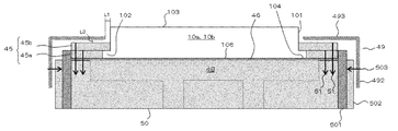
- FIG. 3 is a schematic diagram showing an example of a cross-sectional structure around the gas flow sputtering flat targets 10a and 10b and the fixing member 45 according to the present invention when the backing plate 47 is not used.
- the target has an attachment portion 102 extending from the side surface 101, and the attachment portion 102 is sandwiched between the conductive fixing member 45 and the cooling device 50 via a diaphragm (indirect cooling plate) 46.
- the target is fixed to the cooling device 50.
- a configuration may also be adopted in which the target is fixed to the cooling device 50 in a positional relationship in which the attachment portion 102 is directly sandwiched between the conductive fixing member 45 and the cooling device 50 without the diaphragm 46 interposed.
- the cooling efficiency is higher when the diaphragm 46 is not present. In this case, it is necessary to remove the cooling water 48 in order to prevent the cooling water 48 from leaking out of the cooling device 50 when the inside of the sputtering chamber 11 is evacuated. Therefore, it is preferable to install the diaphragm 46 from the viewpoint of maintainability.
- the attachment portion 102 can be formed by integrally molding with the flat plate target main body portion.
- the region where the attachment part 102 is installed is not particularly limited as long as the flat targets 10a and 10b can be fixed to the cooling device 50, but the attachment part 102 is continuously provided so as to surround the side surface 101 of the flat targets 10a and 10b. It may be provided, or may be provided intermittently at a plurality of locations as many as necessary to fix the flat targets 10 a and 10 b to the cooling device 50. From the viewpoint of the workability of the flat targets 10a and 10b and the strength of the attachment portions, the attachment portions 102 are preferably provided continuously so as to surround the side surface 101 of the flat targets 10a and 10b.
- the conductive fixing member 45 sandwiching the attachment portion 102 does not protrude above the upper surfaces (sputter surfaces) 103 of the flat targets 10a and 10b. For this reason, it is preferable that the upper surface of the attachment part 102 extended from the side surface 101 is in a position lower than the upper surfaces 103 of the flat targets 10a and 10b. In this case, when the cross section of the target is observed, a step is generated between the upper surface 103 of the flat targets 10a and 10b and the upper surface of the attachment portion 102.
- the lower surface 104 of the attachment portion 102 extending from the side surface 101 is at the same height as the lower surface 106 of the flat targets 10a and 10b. It is preferable. That is, the lower surface 106 of the flat targets 10a and 10b and the lower surface 104 of the attachment site 102 are preferably on the same plane.
- the material of the conductive fixing member 45 is not particularly limited, but preferably has heat resistance.
- the heat-resistant conductive material include metals, particularly metals having a melting point higher than the melting point of aluminum (660.3 ° C.), metals having a melting point of 700 ° C. or higher are more preferable, and temperatures of 800 ° C. or higher are preferable.
- a metal having a melting point is even more preferred, and a metal having a melting point of 1000 ° C. or higher is even more preferred.
- Carbon such as graphite can also be used.
- a material selected from the group consisting of iron, copper, titanium, niobium, tantalum, tungsten, molybdenum, cobalt, chromium, nickel, and graphite may be used alone, or an alloy that combines two or more types (stainless steel may also be used). Or metal-graphite composites may be used. Among these, stainless steel is preferable because of its high strength, easy availability, and low cost.
- the shape and dimensions of the conductive fixing member 45 are not particularly limited as long as the flat plate targets 10 a and 10 b can be fixed to the cooling device 50 in a positional relationship where the attachment site 102 is sandwiched between the conductive fixing member 45 and the cooling device 50.
- the upper surface of the conductive fixing member 45 preferably does not protrude above the upper surfaces of the flat targets 10a and 10b, and is lower than the upper surfaces of the flat targets 10a and 10b. It is more preferable.
- the conductive fixing member 45 may be configured as an integrally molded product, or may be configured by combining two or more components. For example, in the embodiment shown in FIG.
- the conductive fixing member 45 is the same as the lower surface 104 of the attachment site 102.
- a frame-shaped first fixing component 45a having a lower surface on a plane, an upper surface on the same plane as the upper surface of the mounting portion 102, and an inner surface closely contacting the side surface of the mounting portion 102, and placed on the first fixing component 45a
- the second fixed component 45b is formed on the lower surface on the same plane as the upper surface of the attachment portion 102, the upper surface at a position lower than the upper surface 103 of the flat targets 10a and 10b, and the side surface 101 of the flat targets 10a and 10b.
- first fixing component 45a and the second fixing component 45b are in contact with each other so that the outer surfaces of the first fixing component 45a and the second fixing component 45b are continuous without a step, thereby simplifying the sputtering apparatus and the shield shape.
- first fixing component 45a and the second fixing component 45b can each be provided as a rectangular frame.
- the conductive fixing member 45 is not sputtered. If the conductive fixing member 45 is sputtered, a desired sputtered film composition cannot be obtained, and the maintenance frequency of the conductive fixing member 45 is increased, which is disadvantageous. Further, although it is ideal that the total amount of sputtered particles is deposited on the member 16, if the sputter rate is increased to increase the production efficiency, a lot of sputtered particles are scattered around the flat plate targets 10a and 10b. As a result, sputtered particles accumulate on the conductive fixing member 45 and are likely to spread further to the periphery.
- the conductive fixing member 45 is covered with the insulating shield member 49.
- the insulating shield member 49 can function as a member for depositing sputtered particles.
- the insulating shield member 49 includes a side plate 492 that covers the outer surface of the conductive fixing member 45 and an upper surface plate 493 that covers the upper surface of the conductive fixing member 45.
- the distance L3 between the lower surface of the upper surface plate 493 of the insulating shield member 49 and the upper surface of the conductive fixing member 45 is 10 mm or less. Is preferably 5 mm or less, and more preferably 2 mm or less. Even if the lower surface of the upper surface plate 493 of the insulating shield member 49 and the upper surface of the conductive fixing member 45 are in contact with each other, it does not cause abnormal discharge, so L3 may be zero.
- the insulating shield member 49 is made of a heat resistant material.
- the insulation resistance of the insulating shield member 49 is preferably 1 kV or more, more preferably 2 kV or more, and even more preferably 10 kV or more, with respect to the thickness of the member to be installed.
- the heat-resistant material constituting the insulating shield member 49 one kind selected from the group consisting of aluminum oxide, silicon oxide, zirconium oxide, magnesium oxide, yttrium oxide, calcium oxide, titanium oxide, and boron nitride is used. Or 2 or more types are mentioned. With these materials, it is easy to collect the adhering sputtered particles.
- the insulating shield member 49 does not contact the targets 10a and 10b.
- the conductive fixing member 45 is The portion that is not covered with the insulating shield member 49 becomes large, and the effect of preventing the conductive fixing member 45 from being sputtered is weakened. Therefore, it is preferable to adjust the closest distance (L1) between each target 10a, 10b and the insulating shield member 49 to 0.1 mm or more when the pair of flat targets 10a, 10b are viewed in plan. It is more preferable to adjust to 3 mm or more, and even more preferable to adjust to 0.5 mm or more.
- the closest distance (L1) is preferably adjusted to 5 mm or less, more preferably adjusted to 3 mm or less, and even more preferably adjusted to 1 mm or less.
- the closest gap (L1) is generated between the targets 10a and 10b and the insulating shield member 49.
- an insulating shield is provided so as to cover the edge of the upper surface (sputtered surface) 103 of each flat target 10a, 10b.
- An aspect in which the member 49 is arranged is also possible. Even in this case, it is preferable to adjust the closest distance (L1) between the targets 10a and 10b and the insulating shield member 49 to the range as described above.
- the insulating shield member 49 may be covered with another shield member so that the deposition of sputtered particles on the insulating shield member 49 is suppressed.
- the shield member in this case desirably has heat resistance, but it does not matter whether it is conductive or insulating.
- the discharge voltage increases as the discharge power is increased, and thus arc discharge occurs between the shield member 49 and the conductive fixing member 45. Since the risk becomes high, it is necessary to make the shield member 49 insulative in order to perform stable sputtering for a long period of time.
- the cooling device 50 Since the cooling device 50 is in contact with each of the flat targets 10a and 10b, it can be a cathode potential. Therefore, in order to prevent the cooling device 50 from being sputtered, it is preferable to arrange the insulating shield member 501 for the cooling device so as to cover the outer surface of the cooling device 50.
- the insulating shield member 501 can obtain a spatter prevention effect by covering at least a part of the outer surface of the cooling device 50, but it is preferable that the entire outer surface is covered.
- the insulating shield member 501 can be directly on the outer surface of the cooling device 50. Suitable materials for the insulating shield member 501 for the cooling device are as described in the insulating shield member 49.
- FIG. 7 is a schematic diagram showing an example of a cross-sectional structure of the flat plate targets 10a and 10b for gas flow sputtering according to the present invention when the backing plate 47 is used.
- the role of each component indicated by the same reference numeral and preferred modes thereof are as described in FIG. 3, and redundant description will be omitted, and the description will focus on a configuration different from the embodiment of FIG. 3.
- a portion of the backing plate 47 extends from the side surface 101 to form an attachment site 102.
- the target is fixed to the cooling device 50 in a positional relationship in which the attachment portion 102 is directly sandwiched between the conductive fixing member 45 and the cooling device 50.
- the backing plate 47 since the backing plate 47 exists, there is no possibility that the cooling water leaks out when the inside of the sputtering chamber 11 is evacuated, and therefore it is not necessary to interpose the diaphragm 46.
- the shape and dimensions of the conductive fixing member 45 are such that the targets 10a and 10b can be fixed to the cooling device 50 in a positional relationship in which the attachment site 102 is sandwiched between the conductive fixing member 45 and the cooling device 50.
- the conductive fixing member 45 is an integrally molded product, a lower surface on the same plane as the upper surface of the attachment site 102, an upper surface located at a position lower than the upper surface 103 of the flat targets 10 a and 10 b, and
- the frame structure has an inner surface that is in close contact with the side surface 101 of the flat targets 10a and 10b.
- the conductive fixing member 45 can be provided as a rectangular frame.
- the insulating shield member 49 has a peripheral wall 491 erected so as to surround the side surface 101 at an interval L1 along the side surface 101 of the flat targets 10a and 10b. . Due to the presence of the peripheral wall 491, the side surfaces of the flat targets 10a and 10b are hidden, so that the discharge is easily stabilized. In addition, it can be expected that the conductive fixing member 45 of plasma is hardly sputtered.
- the peripheral wall 491 is not essential, and a mode in which the peripheral wall 491 is not provided as shown in FIG. 5 is also possible. Further, as shown in FIG. 6, the upper surface plate 493 of the insulating shield member 49 can be thickened to increase the strength of the insulating shield member. Since the target side surface can also be hidden by this mode, the same effect as the peripheral wall 491 can be expected.
- the configuration of the insulating shield member 49 is not limited to the embodiment shown in FIGS. 3 to 7, and other embodiments can be adopted.
- the insulating shield member 49 has no side plate 492.
- the fastener mounting base 502 covers the top plate 493 and the side plate 492 of the insulating shield member 49.
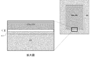
- FIG. 8 is a plan view showing an example of the positional relationship between the flat targets 10a and 10b and the insulating shield member 49 when the rectangular flat targets 10a and 10b are used.
- rectangular flat targets 10 a and 10 b are disposed so as to be surrounded by a peripheral wall 491 of a rectangular frame-shaped insulating shield member 49.
- the distance L1 between the side surface 101 of the flat target 10a, 10b and the peripheral wall 491 of the insulating shield member 49 is preferably 0.1 mm or more, more preferably 0.2 mm or more in order to maintain stable discharge. Still more preferably, it is 0.3 mm or more. Further, the distance L1 is preferably 2 mm or less, more preferably 1.5 mm or less, and even more preferably 1 mm or less for the reason that the fixing member 45 is prevented from being sputtered.
- the conductive fixing member 45 and, when installed, one or more through holes are provided in the diaphragm 46, and further attached to the cooling device 50.
- a hole is provided and a fastener 51 such as a bolt or a screw is inserted into the through hole and the mounting hole in order and fixed (see FIGS. 3 to 6).
- One or two or more through holes may be provided in the attachment site 102 and the fastener 51 may be inserted (see FIG. 7).
- a through hole is provided in the insulating shield member 49, and a mounting hole is also provided in the insulating shield member 501 for the cooling device, and the through hole and the mounting hole are sequentially provided.
- a method of inserting and fixing fasteners 503 such as bolts and screws can be used.
- the fastener 503 is made of metal, it is preferable to ground the fastener 503 to an anode potential in order to prevent the fastener 503 from being sputtered.
- a metal is preferable from an insulating material such as ceramics from the viewpoint of durability.
- a metal fastener mounting base 502 may be installed on the outer surface of the insulating shield member 501 for the cooling device, and a mounting hole may be provided in the fastener mounting base 502.
- the fastener mounting base 502 can be disposed directly on the outer surface of the insulating shield member 501 so as to surround the outer surface of the insulating shield member 501.
- the fastener 503 is made of metal, it is preferable to ground the fastener 503 to an anode potential in order to prevent the fastener 503 from being sputtered.
- the sputtering rate 0.005g / h / cm 2 or more, preferably 0.01g / h / cm 2 or more, more preferably 0.02 g / h / Continuous sputtering can be performed without abnormal discharge for 5 hours or more at cm 2 or more, for example 0.005 to 0.1 g / h / cm 2 .
- the reference area of the sputtering rate refers to the total area of the sputtering surfaces of the opposing targets (here, the total of the projected areas of the opposing sputtering surfaces of the pair of flat plate targets).
- the sputtered film obtained by sputtering using the gas flow sputtering apparatus according to the present invention is peeled off and collected from the member on which the sputtered particles are deposited, and then pulverized to obtain a sputtering target material. be able to.
- a sputtering target can be manufactured by sintering this raw material.
- the present invention is useful as a method for efficiently producing a non-magnetic material particle-dispersed sputtering target with a refined structure.
- the total mass of the sputtered particles deposited on the insulating shield member 49 is deposited on the member 16 for depositing the sputtered particles.
- the mass of sputtered particles can be made larger.
- the ratio of the total mass of sputtered particles deposited on the insulating shield member 49 to the mass of sputtered particles deposited on the member 16 can be 2 or more, can be 3 or more, and can be 4 or more. You can also For this reason, it is also important to improve the production efficiency to collect the sputtered particles deposited on the insulating shield member 49 and use it as a raw material for the sputtering target.
- the sputtering gas discharge units were arranged in a row with a large number of gas discharge ports over the entire length of the slit serving as the inlet of the space portion 12.
- the number of discharge ports of the sputtering gas discharge unit was 20.
- the shape of the first fixed component was a rectangular frame, and the material of the first fixed component was stainless steel.
- the shape of the second fixed part was a rectangular frame, and the material of the second fixed part was stainless steel.
- Test Example 1 the interval adjusting mechanism was not used, and sputtering was continued for the above sputtering time.
- mean spacing S 1 between the pair of flat plates targets exceed 37 mm (about 100 hours total sputtering time)
- abnormal discharge increased from the vicinity, making it difficult to maintain stable sputtering.
- the sputter rate for this test was 0.062 g / h / cm 2 .
- the ratio of the increased weight of the deposition target substrate to the decreased weight of the target after the sputtering test was 22%.
- the ratio of the increased weight of the insulating shield member to the decreased weight of the target after the sputtering test was 51%.
- the mean spacing S 1 between the pair of flat plate target during the test was measured by calipers.
- Test Example 2 Based on the relationship between the discharge time and the integrated power obtained in Test Example 1 and the average reduction amount of the target thickness, the distance adjustment mechanism is used so that the change width of the average distance between the pair of flat plate targets is 5 mm or less during sputtering.
- a sputtered film was formed under the same conditions as in Test Example 1 except that the interval was manually adjusted.
- the sputter rate for this test was 0.069 g / h / cm 2 .
- the ratio of the increased weight of the deposition target substrate to the decreased weight of the target after the sputtering test was 26%.
- the ratio of the increased weight of the insulating shield member to the decreased weight of the target after the sputtering test was 46%.
- Test Example 3 During sputtering, the chamber is opened periodically (every 10 hours) and the weight of a pair of flat plate targets is measured to calculate the change width of the average interval, and the interval adjustment mechanism is used so that the change width is 5 mm or less.
- a sputtered film was formed under the same conditions as in Test Example 1 except that the interval was manually adjusted. As a result, during the test, a total of 250 hours of sputtering time could pass without causing abnormal discharge.
- the sputter rate for this test was 0.067 g / h / cm 2 .
- the ratio of the increased weight of the deposition target substrate to the decreased weight of the target after the sputtering test was 25%.
- the ratio of the increased weight of the insulating shield member to the decreased weight of the target after the sputtering test was 48%.
- Test Example 4 Verification of the effect of insulating shield members> (Test Example 4) A sputtered film was formed under the same sputtering conditions as in Test Example 1 except that the insulating shield member was removed and the sputter test was performed. In this case, abnormal discharge occurred between the target fixing component and the other anode potential member, and stable film formation could not be performed, and film formation was stopped immediately after the start. When the inside of the sputtering chamber was confirmed, abnormal discharge marks remained on the surfaces of the target and the fixing member.
- Test Example 5 A sputtered film was formed under the same sputtering conditions as in Test Example 1, except that the distance L1 between the flat plate target and the insulating shield member was set to 0 and both were brought into contact. In this case, abnormal discharge frequently occurred between the target and the insulating shield, and the film formation was stopped in 30 minutes.
- the sputter rate for this test was 0.064 g / h / cm 2 .
- the ratio of the increased weight of the deposition target substrate to the decreased weight of the target after the sputtering test was 31%.
- the ratio of the increased weight of the insulating shield member to the decreased weight of the target after the sputtering test was 44%.
- Test Example 6 A sputtered film was formed under the same sputtering conditions as in Test Example 1 except that the distance L1 between the flat target and the insulating shield member was set to 2.2 mm. In this case, there was little abnormal discharge at the beginning of film formation and stable film formation was possible, but abnormal discharge occurred frequently after 3 hours and the discharge was stopped. When the inside of the sputtering chamber was confirmed, the fixing member was also sputtered. The sputter rate for this test was 0.062 g / h / cm 2 . The ratio of the increased weight of the deposition target substrate to the decreased weight of the target after the sputtering test was 25%. The ratio of the increased weight of the insulating shield member to the decreased weight of the target after the sputtering test was 44%.
- Test Example 7 A sputtered film was formed under the same sputtering conditions as in Test Example 1 except that the distance L1 between the flat plate target and the insulating shield member was set to 0.1 mm. In this case, there was little abnormal discharge at the beginning of film formation and stable film formation was possible, but abnormal discharge occurred frequently after 2 hours and the discharge was stopped. When the inside of the sputtering chamber was confirmed, abnormal discharge marks remained between the target and the insulating shield. The sputter rate for this test was 0.067 g / h / cm 2 . The ratio of the increased weight of the deposition target substrate to the decreased weight of the target after the sputtering test was 30%. The ratio of the increased weight of the insulating shield member to the decreased weight of the target after the sputtering test was 51%.
- Test Example 8 A sputtered film was formed under the same sputtering conditions as in Test Example 1 except that the distance L1 between the flat target and the insulating shield member was 1.5 mm. In this case, there was little abnormal discharge and stable film formation was achieved, and film formation was completed as scheduled after 5 hours. However, when the inside of the sputtering chamber was confirmed, the fixing member was also sputtered. The sputter rate for this test was 0.069 g / h / cm 2 . The ratio of the increased weight of the deposition target substrate to the decreased weight of the target after the sputtering test was 26%. The ratio of the increased weight of the insulating shield member to the decreased weight of the target after the sputtering test was 46%.
- Test Example 9 A sputtered film was formed under the same sputtering conditions as in Test Example 1 except that the gas flow sputtering conditions were changed as follows. ⁇ Power density: 22 W / cm 2 ⁇ Sputtering gas pressure: 70Pa Sputtering gas flow rate (sum of flow rate from each discharge port): Ar: 32.7 sccm / cm 2 ⁇ Target material: Cu-TiO 2 -SiO 2 ⁇ Target relative density: 95% -Distance L1 between flat plate target and insulating shield member: 0.4mm ⁇ Spacing between a pair of flat plate targets before the start of sputtering S 1 : 20 mm In this case, there was little abnormal discharge and stable film formation was achieved, and film formation was completed as scheduled after 5 hours.
- the sputter rate for this test was 0.013 g / h / cm 2 .
- the ratio of the increased weight of the deposition target substrate to the decreased weight of the target after the sputtering test was 28%.
- the ratio of the increased weight of the insulating shield member to the decreased weight of the target after the sputtering test was 48%.
- the sputtered film of Test Example 9 was separated from the substrate and collected. And this film
- the conditions for hot isostatic pressing were a heating rate of 300 ° C./hour, a holding temperature of 1000 ° C., a holding time of 2 hours, and gradually increasing the Ar gas pressure from the beginning of the heating and holding at 1000 ° C.
- Test Example 10 A sputtered film was formed under the same sputtering conditions as in Test Example 1 except that the gas flow sputtering conditions were changed as follows. ⁇ Gas flow sputtering conditions> ⁇ Power density: 28W / cm 2 ⁇ Sputtering gas pressure: 25Pa Sputtering gas flow rate (sum of the flow rate from each discharge port): Ar: 14.2 sccm / cm 2 ⁇ Target material: Cu-TiO 2 ⁇ Target relative density: 97% Target size: 143 mm (X direction) x 493 mm (Y direction) x 30 mmt Target total projected area: 1410 cm 2 -Distance L1 between flat plate target and insulating shield member: 0.8mm In this case, there was little abnormal discharge and stable film formation was achieved, and film formation was completed as scheduled after 5 hours.
- the sputter rate for this test was 0.011 g / h / cm 2 .
- the ratio of the increased weight of the deposition target substrate to the decreased weight of the target after the sputtering test was 40%.
- the ratio of the increased weight of the insulating shield member to the decreased weight of the target after the sputtering test was 42%.
- Test Example 11 A flat plate target-facing gas flow sputtering apparatus having the configuration shown in FIGS. 1 and 2-1 (however, the sputtering target mounting structure adopts the structure shown in FIG. 4) is used, and the sputtering target is mounted in the configuration shown in FIG. Then, a sputtered film was formed under the following conditions. A sputtered film was formed with the same apparatus configuration and sputtering conditions as in Test Example 1, except that the gas flow sputtering conditions were changed as follows.
- Test Example 12 A flat plate target-facing gas flow sputtering apparatus having the configuration shown in FIGS. 1 and 2-1 (however, the sputtering target mounting structure adopts the structure shown in FIG. 5) is used, and the sputtering target is mounted in the configuration shown in FIG. Then, a sputtered film was formed under the following conditions. A sputtered film was formed with the same apparatus configuration and sputtering conditions as in Test Example 1, except that the gas flow sputtering conditions were changed as follows.
- Test Example 13 A flat plate target-facing gas flow sputtering apparatus having the configuration shown in FIGS. 1 and 2-1 (however, the sputtering target mounting structure adopts the structure shown in FIG. 6) is used, and the sputtering target is mounted in the configuration shown in FIG. Then, a sputtered film was formed under the following conditions. A sputtered film was formed with the same apparatus configuration and sputtering conditions as in Test Example 1, except that the gas flow sputtering conditions were changed as follows.
- the sputter rate for this test was 0.007 g / h / cm 2 .
- Test Example 14 A flat plate target-facing gas flow sputtering apparatus having the configuration shown in FIGS. 1 and 2-1 (however, the sputtering target mounting structure adopts the structure shown in FIG. 7) is used, and the sputtering target is mounted in the configuration shown in FIG. Then, a sputtered film was formed under the following conditions. A sputtered film was formed with the same apparatus configuration and sputtering conditions as in Test Example 1, except that the gas flow sputtering conditions were changed as follows.
- the sputter rate for this test was 0.033 g / h / cm 2 .
- the ratio of the increased weight of the deposition target substrate to the decreased weight of the target after the sputtering test was 24%.
- the ratio of the increased weight of the insulating shield member to the decreased weight of the target after the sputtering test was 48%.
Landscapes
- Chemical & Material Sciences (AREA)
- Chemical Kinetics & Catalysis (AREA)
- Engineering & Computer Science (AREA)
- Materials Engineering (AREA)
- Mechanical Engineering (AREA)
- Metallurgy (AREA)
- Organic Chemistry (AREA)
- Physical Vapour Deposition (AREA)
- Manufacturing Of Magnetic Record Carriers (AREA)
Priority Applications (1)
| Application Number | Priority Date | Filing Date | Title |
|---|---|---|---|
| CN201780078453.8A CN110100042B (zh) | 2016-12-28 | 2017-12-11 | 气流溅射装置以及溅射靶原料的制造方法 |
Applications Claiming Priority (2)
| Application Number | Priority Date | Filing Date | Title |
|---|---|---|---|
| JP2016256657A JP7005896B2 (ja) | 2016-12-28 | 2016-12-28 | ガスフロースパッタリング装置及びスパッタリングターゲット原料の製造方法 |
| JP2016-256657 | 2016-12-28 |
Publications (1)
| Publication Number | Publication Date |
|---|---|
| WO2018123550A1 true WO2018123550A1 (ja) | 2018-07-05 |
Family
ID=62708037
Family Applications (1)
| Application Number | Title | Priority Date | Filing Date |
|---|---|---|---|
| PCT/JP2017/044448 Ceased WO2018123550A1 (ja) | 2016-12-28 | 2017-12-11 | ガスフロースパッタリング装置及びスパッタリングターゲット原料の製造方法 |
Country Status (5)
| Country | Link |
|---|---|
| JP (2) | JP7005896B2 (https=) |
| CN (1) | CN110100042B (https=) |
| SG (1) | SG10202105751VA (https=) |
| TW (1) | TWI660060B (https=) |
| WO (1) | WO2018123550A1 (https=) |
Citations (4)
| Publication number | Priority date | Publication date | Assignee | Title |
|---|---|---|---|---|
| JP2009066497A (ja) * | 2007-09-12 | 2009-04-02 | Bridgestone Corp | 光触媒酸化チタン薄膜及びその製造方法 |
| JP2012144793A (ja) * | 2011-01-13 | 2012-08-02 | Sumitomo Heavy Ind Ltd | ターゲット、およびこれを備えた成膜装置 |
| JP2013147711A (ja) * | 2012-01-20 | 2013-08-01 | Renesas Electronics Corp | 気相成長装置 |
| WO2013136962A1 (ja) * | 2012-03-15 | 2013-09-19 | Jx日鉱日石金属株式会社 | 磁性材スパッタリングターゲット及びその製造方法 |
Family Cites Families (2)
| Publication number | Priority date | Publication date | Assignee | Title |
|---|---|---|---|---|
| EP0824760A1 (en) * | 1995-05-11 | 1998-02-25 | Materials Research Corporation | Sputtering apparatus with isolated coolant and sputtering target therefor |
| JP2004183022A (ja) * | 2002-12-02 | 2004-07-02 | Ulvac Japan Ltd | ターゲット装置及びスパッタリング装置 |
-
2016
- 2016-12-28 JP JP2016256657A patent/JP7005896B2/ja active Active
-
2017
- 2017-12-11 SG SG10202105751VA patent/SG10202105751VA/en unknown
- 2017-12-11 CN CN201780078453.8A patent/CN110100042B/zh active Active
- 2017-12-11 WO PCT/JP2017/044448 patent/WO2018123550A1/ja not_active Ceased
- 2017-12-25 TW TW106145564A patent/TWI660060B/zh not_active IP Right Cessation
-
2021
- 2021-05-24 JP JP2021087172A patent/JP2021127524A/ja active Pending
Patent Citations (4)
| Publication number | Priority date | Publication date | Assignee | Title |
|---|---|---|---|---|
| JP2009066497A (ja) * | 2007-09-12 | 2009-04-02 | Bridgestone Corp | 光触媒酸化チタン薄膜及びその製造方法 |
| JP2012144793A (ja) * | 2011-01-13 | 2012-08-02 | Sumitomo Heavy Ind Ltd | ターゲット、およびこれを備えた成膜装置 |
| JP2013147711A (ja) * | 2012-01-20 | 2013-08-01 | Renesas Electronics Corp | 気相成長装置 |
| WO2013136962A1 (ja) * | 2012-03-15 | 2013-09-19 | Jx日鉱日石金属株式会社 | 磁性材スパッタリングターゲット及びその製造方法 |
Also Published As
| Publication number | Publication date |
|---|---|
| JP7005896B2 (ja) | 2022-01-24 |
| TWI660060B (zh) | 2019-05-21 |
| TW201827632A (zh) | 2018-08-01 |
| SG10202105751VA (en) | 2021-07-29 |
| CN110100042B (zh) | 2021-12-07 |
| JP2021127524A (ja) | 2021-09-02 |
| JP2018109206A (ja) | 2018-07-12 |
| CN110100042A (zh) | 2019-08-06 |
Similar Documents
| Publication | Publication Date | Title |
|---|---|---|
| CN101801565B (zh) | 具有均匀无序晶体学取向的细晶无带的难熔金属溅射靶、薄膜制备方法及基于薄膜的器件和由器件制造的产品 | |
| US6494999B1 (en) | Magnetron sputtering apparatus with an integral cooling and pressure relieving cathode | |
| JP5876138B2 (ja) | 磁性材スパッタリングターゲット及びその製造方法 | |
| US8016982B2 (en) | Sputtering apparatus and sputtering method | |
| JP2008001988A (ja) | 改善されたpvdターゲット | |
| US9476117B2 (en) | Hot tile sputtering system | |
| KR20070085127A (ko) | 냉각 타겟을 사용한 스퍼터링 | |
| US20120118733A1 (en) | Magnetron sputtering apparatus | |
| US20210272785A1 (en) | Physical Vapor Deposition Processing Systems Target Cooling | |
| US10381203B2 (en) | Backing plate obtained by diffusion-bonding anticorrosive metal and Mo or Mo alloy, and sputtering target-backing plate assembly provided with said backing plate | |
| WO2018123549A1 (ja) | ガスフロースパッタリング装置、ガスフロースパッタ用ターゲット及びスパッタリングターゲット原料の製造方法 | |
| WO2018123550A1 (ja) | ガスフロースパッタリング装置及びスパッタリングターゲット原料の製造方法 | |
| KR20120094086A (ko) | Ito 스퍼터링 타깃 | |
| JP4639764B2 (ja) | 円筒状ターゲット及び成膜方法 | |
| CN107995932B (zh) | 磁控溅射阴极系统 | |
| US20070285839A1 (en) | Perpendicular magnetic recording medium and method of manufacturing the same | |
| WO2020158272A1 (ja) | ターゲットおよび成膜装置並びに成膜対象物の製造方法 | |
| TW201610197A (zh) | 濺鍍靶-背板接合體 | |
| JP5246017B2 (ja) | スパッタリング装置 | |
| JPH0967668A (ja) | スパッタターゲット | |
| WO2021157112A1 (ja) | スパッタリングターゲット | |
| KR20170051670A (ko) | 루테늄 스퍼터링 타겟 제조방법 | |
| KR20140108349A (ko) | 스퍼터링 타깃 | |
| JP2006131968A (ja) | 円筒状マグネトロンスパッタ装置 | |
| JPS6119773A (ja) | スパツタ装置 |
Legal Events
| Date | Code | Title | Description |
|---|---|---|---|
| 121 | Ep: the epo has been informed by wipo that ep was designated in this application |
Ref document number: 17888129 Country of ref document: EP Kind code of ref document: A1 |
|
| NENP | Non-entry into the national phase |
Ref country code: DE |
|
| 122 | Ep: pct application non-entry in european phase |
Ref document number: 17888129 Country of ref document: EP Kind code of ref document: A1 |