WO2018117239A1 - 液晶配向膜の製造方法、液晶配向膜、及び液晶表示素子 - Google Patents
液晶配向膜の製造方法、液晶配向膜、及び液晶表示素子 Download PDFInfo
- Publication number
- WO2018117239A1 WO2018117239A1 PCT/JP2017/046015 JP2017046015W WO2018117239A1 WO 2018117239 A1 WO2018117239 A1 WO 2018117239A1 JP 2017046015 W JP2017046015 W JP 2017046015W WO 2018117239 A1 WO2018117239 A1 WO 2018117239A1
- Authority
- WO
- WIPO (PCT)
- Prior art keywords
- liquid crystal
- alignment film
- crystal alignment
- group
- formula
- Prior art date
- Legal status (The legal status is an assumption and is not a legal conclusion. Google has not performed a legal analysis and makes no representation as to the accuracy of the status listed.)
- Ceased
Links
- 0 O=C(*1(CCC(O2)=O)C2=O)OC1=O Chemical compound O=C(*1(CCC(O2)=O)C2=O)OC1=O 0.000 description 7
- URLKBWYHVLBVBO-UHFFFAOYSA-N Cc1ccc(C)cc1 Chemical compound Cc1ccc(C)cc1 URLKBWYHVLBVBO-UHFFFAOYSA-N 0.000 description 2
- DBZVBKLKGDGTQE-UHFFFAOYSA-N CC(C)(c(cc1)ccc1Oc1ccc(C)cc1)c(cc1)ccc1Oc1ccc(C)cc1 Chemical compound CC(C)(c(cc1)ccc1Oc1ccc(C)cc1)c(cc1)ccc1Oc1ccc(C)cc1 DBZVBKLKGDGTQE-UHFFFAOYSA-N 0.000 description 1
- YXBIAYXZUDJVEB-UHFFFAOYSA-N Cc(cc1)c(C)cc1-c1cc(C)c(C)cc1 Chemical compound Cc(cc1)c(C)cc1-c1cc(C)c(C)cc1 YXBIAYXZUDJVEB-UHFFFAOYSA-N 0.000 description 1
- PZCRCGZQRHMEDY-UHFFFAOYSA-N Cc(cc1)cc(C)c1-c1ccc(C)cc1C Chemical compound Cc(cc1)cc(C)c1-c1ccc(C)cc1C PZCRCGZQRHMEDY-UHFFFAOYSA-N 0.000 description 1
- RZTDESRVPFKCBH-UHFFFAOYSA-N Cc(cc1)ccc1-c1ccc(C)cc1 Chemical compound Cc(cc1)ccc1-c1ccc(C)cc1 RZTDESRVPFKCBH-UHFFFAOYSA-N 0.000 description 1
- CHLICZRVGGXEOD-UHFFFAOYSA-N Cc(cc1)ccc1OC Chemical compound Cc(cc1)ccc1OC CHLICZRVGGXEOD-UHFFFAOYSA-N 0.000 description 1
- SCKJMSOLHSTLCC-UHFFFAOYSA-N Cc(cc1)ccc1Oc(cc1)ccc1-c(cc1)ccc1Oc1ccc(C)cc1 Chemical compound Cc(cc1)ccc1Oc(cc1)ccc1-c(cc1)ccc1Oc1ccc(C)cc1 SCKJMSOLHSTLCC-UHFFFAOYSA-N 0.000 description 1
- BZMWYTDVUYRVEI-UHFFFAOYSA-N Cc(cc1)ccc1Oc(cc1)ccc1Oc1ccc(C)cc1 Chemical compound Cc(cc1)ccc1Oc(cc1)ccc1Oc1ccc(C)cc1 BZMWYTDVUYRVEI-UHFFFAOYSA-N 0.000 description 1
- MQXVMEZAAVKSHA-UHFFFAOYSA-N Cc(cc1)ccc1Oc1ccc(C(C(F)(F)F)(C(F)(F)F)c(cc2)ccc2Oc2ccc(C)cc2)cc1 Chemical compound Cc(cc1)ccc1Oc1ccc(C(C(F)(F)F)(C(F)(F)F)c(cc2)ccc2Oc2ccc(C)cc2)cc1 MQXVMEZAAVKSHA-UHFFFAOYSA-N 0.000 description 1
- NRXWFTYEJYEOGW-UHFFFAOYSA-N Cc(cc1)ccc1Sc1ccc(C)cc1 Chemical compound Cc(cc1)ccc1Sc1ccc(C)cc1 NRXWFTYEJYEOGW-UHFFFAOYSA-N 0.000 description 1
- HZAWPPRBCALFRN-UHFFFAOYSA-N Cc1ccc(Cc2ccc(C)cc2)cc1 Chemical compound Cc1ccc(Cc2ccc(C)cc2)cc1 HZAWPPRBCALFRN-UHFFFAOYSA-N 0.000 description 1
- BLFSCTNBQZZCMH-UHFFFAOYSA-N Cc1cccc(Oc2cccc(Oc3cc(C)ccc3)c2)c1 Chemical compound Cc1cccc(Oc2cccc(Oc3cc(C)ccc3)c2)c1 BLFSCTNBQZZCMH-UHFFFAOYSA-N 0.000 description 1
- SDDBCEWUYXVGCQ-UHFFFAOYSA-N Cc1cccc2c(C)cccc12 Chemical compound Cc1cccc2c(C)cccc12 SDDBCEWUYXVGCQ-UHFFFAOYSA-N 0.000 description 1
Classifications
-
- C—CHEMISTRY; METALLURGY
- C08—ORGANIC MACROMOLECULAR COMPOUNDS; THEIR PREPARATION OR CHEMICAL WORKING-UP; COMPOSITIONS BASED THEREON
- C08G—MACROMOLECULAR COMPOUNDS OBTAINED OTHERWISE THAN BY REACTIONS ONLY INVOLVING UNSATURATED CARBON-TO-CARBON BONDS
- C08G73/00—Macromolecular compounds obtained by reactions forming a linkage containing nitrogen with or without oxygen or carbon in the main chain of the macromolecule, not provided for in groups C08G12/00 - C08G71/00
- C08G73/06—Polycondensates having nitrogen-containing heterocyclic rings in the main chain of the macromolecule
- C08G73/10—Polyimides; Polyester-imides; Polyamide-imides; Polyamide acids or similar polyimide precursors
- C08G73/1003—Preparatory processes
- C08G73/1007—Preparatory processes from tetracarboxylic acids or derivatives and diamines
- C08G73/1025—Preparatory processes from tetracarboxylic acids or derivatives and diamines polymerised by radiations
-
- C—CHEMISTRY; METALLURGY
- C08—ORGANIC MACROMOLECULAR COMPOUNDS; THEIR PREPARATION OR CHEMICAL WORKING-UP; COMPOSITIONS BASED THEREON
- C08G—MACROMOLECULAR COMPOUNDS OBTAINED OTHERWISE THAN BY REACTIONS ONLY INVOLVING UNSATURATED CARBON-TO-CARBON BONDS
- C08G73/00—Macromolecular compounds obtained by reactions forming a linkage containing nitrogen with or without oxygen or carbon in the main chain of the macromolecule, not provided for in groups C08G12/00 - C08G71/00
- C08G73/06—Polycondensates having nitrogen-containing heterocyclic rings in the main chain of the macromolecule
- C08G73/10—Polyimides; Polyester-imides; Polyamide-imides; Polyamide acids or similar polyimide precursors
-
- C—CHEMISTRY; METALLURGY
- C08—ORGANIC MACROMOLECULAR COMPOUNDS; THEIR PREPARATION OR CHEMICAL WORKING-UP; COMPOSITIONS BASED THEREON
- C08G—MACROMOLECULAR COMPOUNDS OBTAINED OTHERWISE THAN BY REACTIONS ONLY INVOLVING UNSATURATED CARBON-TO-CARBON BONDS
- C08G73/00—Macromolecular compounds obtained by reactions forming a linkage containing nitrogen with or without oxygen or carbon in the main chain of the macromolecule, not provided for in groups C08G12/00 - C08G71/00
- C08G73/06—Polycondensates having nitrogen-containing heterocyclic rings in the main chain of the macromolecule
- C08G73/10—Polyimides; Polyester-imides; Polyamide-imides; Polyamide acids or similar polyimide precursors
- C08G73/1039—Polyimides; Polyester-imides; Polyamide-imides; Polyamide acids or similar polyimide precursors comprising halogen-containing substituents
-
- C—CHEMISTRY; METALLURGY
- C08—ORGANIC MACROMOLECULAR COMPOUNDS; THEIR PREPARATION OR CHEMICAL WORKING-UP; COMPOSITIONS BASED THEREON
- C08G—MACROMOLECULAR COMPOUNDS OBTAINED OTHERWISE THAN BY REACTIONS ONLY INVOLVING UNSATURATED CARBON-TO-CARBON BONDS
- C08G73/00—Macromolecular compounds obtained by reactions forming a linkage containing nitrogen with or without oxygen or carbon in the main chain of the macromolecule, not provided for in groups C08G12/00 - C08G71/00
- C08G73/06—Polycondensates having nitrogen-containing heterocyclic rings in the main chain of the macromolecule
- C08G73/10—Polyimides; Polyester-imides; Polyamide-imides; Polyamide acids or similar polyimide precursors
- C08G73/1046—Polyimides containing oxygen in the form of ether bonds in the main chain
-
- C—CHEMISTRY; METALLURGY
- C08—ORGANIC MACROMOLECULAR COMPOUNDS; THEIR PREPARATION OR CHEMICAL WORKING-UP; COMPOSITIONS BASED THEREON
- C08L—COMPOSITIONS OF MACROMOLECULAR COMPOUNDS
- C08L79/00—Compositions of macromolecular compounds obtained by reactions forming in the main chain of the macromolecule a linkage containing nitrogen with or without oxygen or carbon only, not provided for in groups C08L61/00 - C08L77/00
- C08L79/04—Polycondensates having nitrogen-containing heterocyclic rings in the main chain; Polyhydrazides; Polyamide acids or similar polyimide precursors
- C08L79/08—Polyimides; Polyester-imides; Polyamide-imides; Polyamide acids or similar polyimide precursors
-
- G—PHYSICS
- G02—OPTICS
- G02F—OPTICAL DEVICES OR ARRANGEMENTS FOR THE CONTROL OF LIGHT BY MODIFICATION OF THE OPTICAL PROPERTIES OF THE MEDIA OF THE ELEMENTS INVOLVED THEREIN; NON-LINEAR OPTICS; FREQUENCY-CHANGING OF LIGHT; OPTICAL LOGIC ELEMENTS; OPTICAL ANALOGUE/DIGITAL CONVERTERS
- G02F1/00—Devices or arrangements for the control of the intensity, colour, phase, polarisation or direction of light arriving from an independent light source, e.g. switching, gating or modulating; Non-linear optics
- G02F1/01—Devices or arrangements for the control of the intensity, colour, phase, polarisation or direction of light arriving from an independent light source, e.g. switching, gating or modulating; Non-linear optics for the control of the intensity, phase, polarisation or colour
- G02F1/13—Devices or arrangements for the control of the intensity, colour, phase, polarisation or direction of light arriving from an independent light source, e.g. switching, gating or modulating; Non-linear optics for the control of the intensity, phase, polarisation or colour based on liquid crystals, e.g. single liquid crystal display cells
- G02F1/133—Constructional arrangements; Operation of liquid crystal cells; Circuit arrangements
- G02F1/1333—Constructional arrangements; Manufacturing methods
- G02F1/1337—Surface-induced orientation of the liquid crystal molecules, e.g. by alignment layers
Definitions
- the present invention relates to a method for producing a liquid crystal alignment film, a liquid crystal alignment film obtained by this production method, and a liquid crystal display device comprising the obtained liquid crystal alignment film.
- Liquid crystal display elements used for liquid crystal televisions, liquid crystal displays, and the like are usually provided with a liquid crystal alignment film for controlling the alignment state of the liquid crystals.
- a liquid crystal alignment film for controlling the alignment state of the liquid crystals.
- the most widely used liquid crystal alignment film in the industry is the surface of a film made of polyamic acid and / or polyimide imidized with a cloth made of cotton, nylon, polyester, etc. formed on an electrode substrate. It is manufactured by performing a so-called rubbing process that rubs in one direction.
- the rubbing process is an industrially useful method that is simple and excellent in productivity.
- scratches on the surface of the alignment film generated by rubbing treatment, dust generation, the influence of mechanical force and static electricity, and even within the alignment processing surface Various problems, such as non-uniformity, have become apparent.
- a liquid crystal alignment treatment method that replaces the rubbing treatment a photo alignment method that imparts liquid crystal alignment ability by irradiating polarized radiation is known.
- As liquid crystal alignment treatment by the photo-alignment method those utilizing a photoisomerization reaction, those utilizing a photocrosslinking reaction, those utilizing a photolysis reaction, etc. have been proposed (see Non-Patent Document 1).
- Patent Document 1 it is proposed to use a polyimide film having an alicyclic structure such as a cyclobutane ring in the main chain for the photo-alignment method.
- the photo-alignment method as described above is a rubbing-less alignment treatment method capable of omitting the rubbing treatment, and can impart liquid crystal alignment ability with an industrially simple manufacturing process.
- a liquid crystal display element of an IPS driving method or a fringe field switching (hereinafter referred to as FFS) driving method a liquid crystal alignment film to which liquid crystal alignment capability is imparted by a photo-alignment method is imparted with liquid crystal alignment capability by rubbing treatment.
- FFS fringe field switching
- the contrast and viewing angle characteristics of the liquid crystal display element can be improved.
- the photo-alignment method as described above has attracted attention as a promising liquid crystal alignment method.
- the liquid crystal alignment film used for the liquid crystal display element of the IPS driving method or the FFS driving method is required to suppress afterimages by long-term alternating current driving in addition to basic properties such as excellent liquid crystal alignment properties and electrical characteristics.
- the liquid crystal alignment film imparted with the liquid crystal aligning ability by the photo-alignment method has a problem that the anisotropy with respect to the alignment direction of the polymer film is smaller than that provided with the liquid crystal aligning ability by rubbing. If the anisotropy is small, sufficient liquid crystal orientation cannot be obtained, and problems such as afterimages occur when a liquid crystal display element is formed.
- the low molecular weight component generated by the main chain of the polyimide being cut by the light irradiation after the light irradiation. Is proposed to be removed (Patent Document 2).
- the remaining low molecular weight compound deteriorates the performance of the liquid crystal display when the removal of the low molecular weight component generated by cutting the main chain of the polyimide is insufficient. Specifically, it has been found that the remaining low molecular compound inhibits the alignment of the liquid crystal to cause alignment unevenness and that the remaining low molecular compound causes a bright spot due to the remaining low molecular compound.
- the low molecular weight component it is necessary to carry out a heat treatment or a contact treatment with an organic solvent. Therefore, the number of steps for producing a liquid crystal alignment film is increased. There was a problem that the yield deteriorated and a higher-quality liquid crystal display element could not be obtained.
- the present invention provides a liquid crystal alignment film capable of suppressing afterimages caused by long-term alternating current driving in liquid crystal display elements of IPS driving method and FFS driving method, and having no defects caused by remaining low molecular weight compounds.
- An object of the present invention is to provide a method for producing a liquid crystal alignment film, the liquid crystal alignment film obtained by the production method, and a liquid crystal display device having the liquid crystal alignment film.
- the present inventors have found that the above object can be achieved by the invention of the following gist.
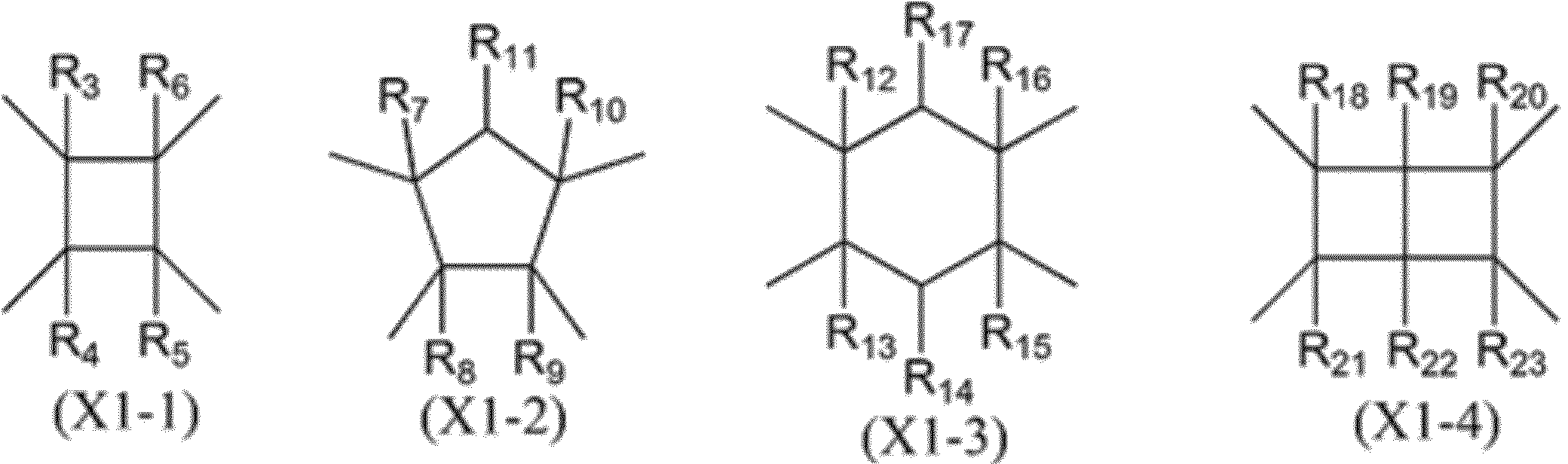
- X 1 is a structure represented by the following formulas (X1-1) to (X1-4).
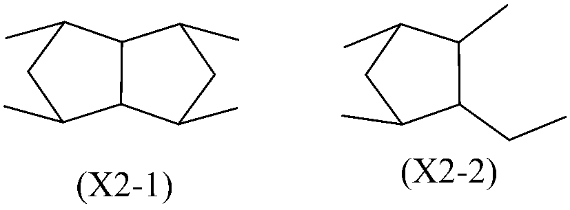
- X 2 is a structure represented by the following formulas (X2-1) to (X2-2).
- R 3 to R 6 are each independently a hydrogen atom, a halogen atom, an alkyl group having 1 to 6 carbon atoms, an alkenyl group having 2 to 6 carbon atoms, an alkynyl group having 2 to 6 carbon atoms, or a carbon containing a fluorine atom. These are monovalent organic groups of 1 to 6 or phenyl groups, which may be the same or different, but at least one is other than a hydrogen atom.
- R 7 to R 23 are each independently a hydrogen atom, a halogen atom, an alkyl group having 1 to 6 carbon atoms, an alkenyl group having 2 to 6 carbon atoms, an alkynyl group having 2 to 6 carbon atoms, or a carbon containing a fluorine atom. These are monovalent organic groups having 1 to 6 or phenyl groups, which may be the same or different.
- the imidization ratio of the polyimide is 10% to 100%.
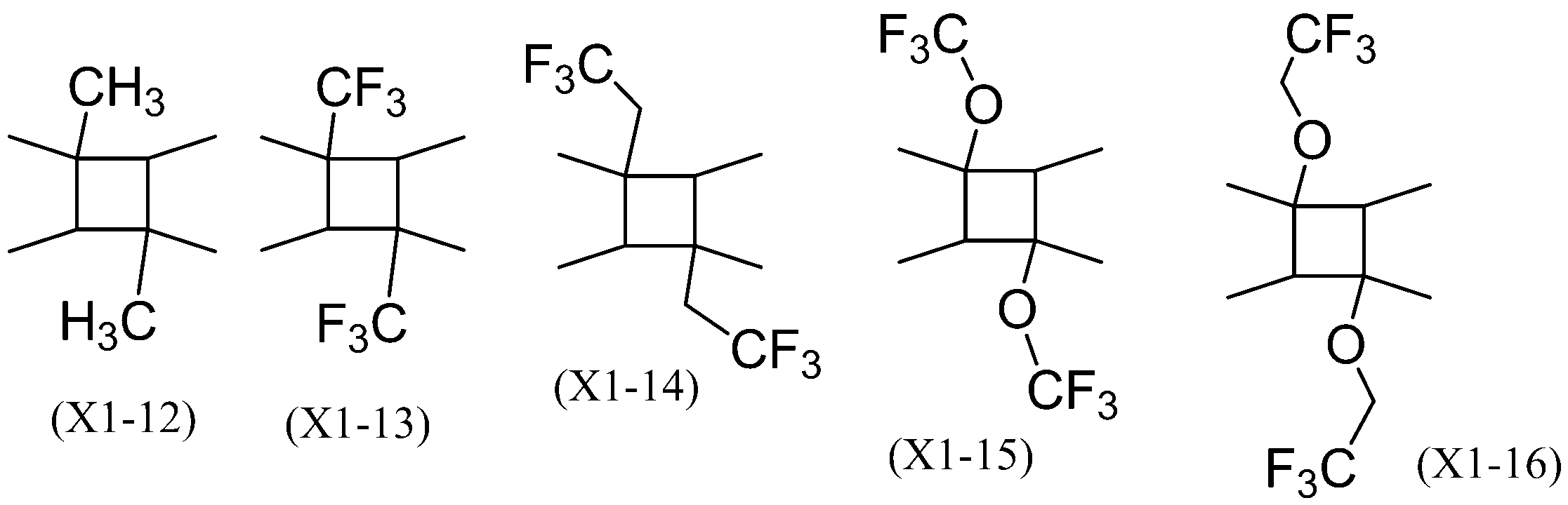
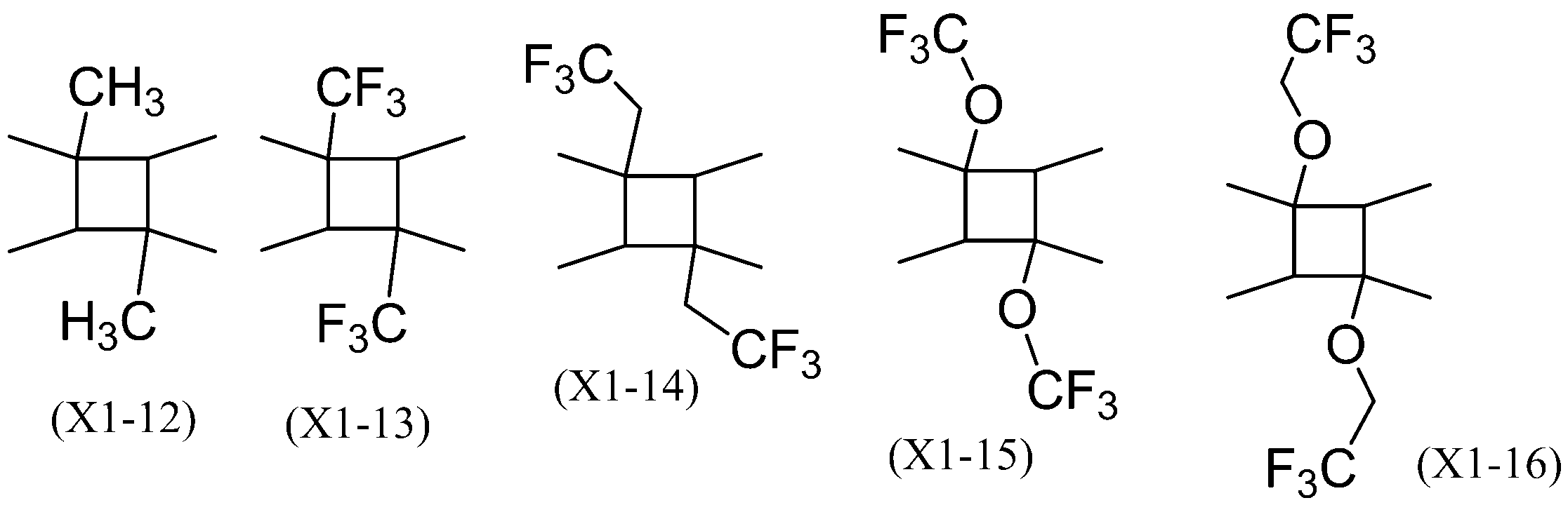
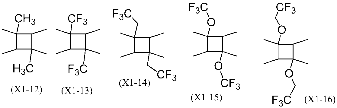
- the structure of X 1 in the formula (1) is at least one selected from structures represented by the following formulas (X1-12) to (X1-16): ⁇ 3.
- the structure of X 1 in the formula (1) is a structure represented by the formula (X1-12). ⁇ 4. The manufacturing method of the liquid crystal aligning film as described in any one of these.
- the structure of X 2 in the formula (2) is a structure represented by the formula (X2-1). ⁇ 5.
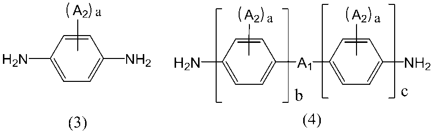
- the diamine component is at least one selected from structures represented by the following formula (3) to the following formula (4). ⁇ 6. The manufacturing method of the liquid crystal aligning film as described in any one of these.
- a 1 is a single bond, an ester bond, an amide bond, a thioester bond, or a divalent organic group having 2 to 20 carbon atoms
- a 2 is a hydrogen atom, a halogen atom, a hydroxyl group, an amino group, a thiol group, a nitro group, Group, a phosphate group, or a monovalent organic group having 1 to 20 carbon atoms
- a is an integer of 1 to 4
- the structures of A 1 may be the same or different.
- b and c are each independently an integer of 1 to 2.
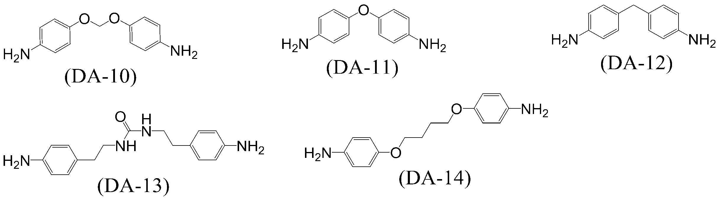
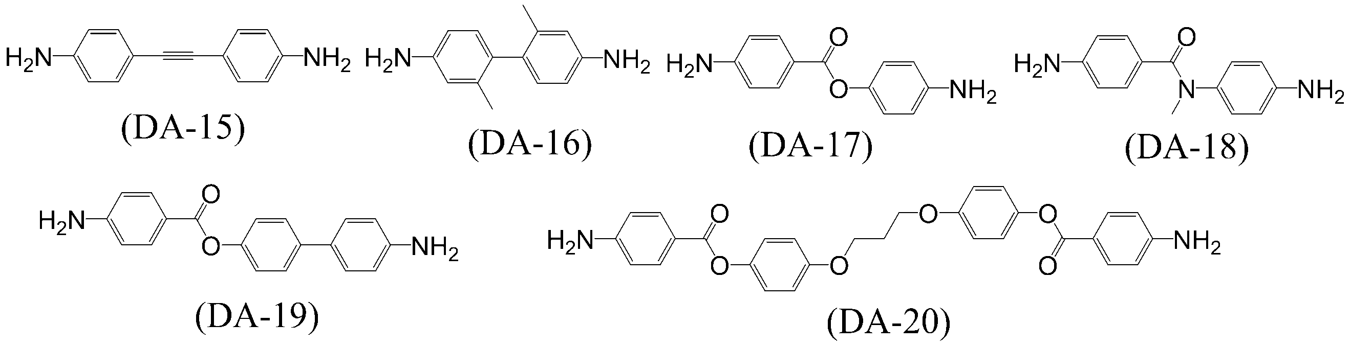
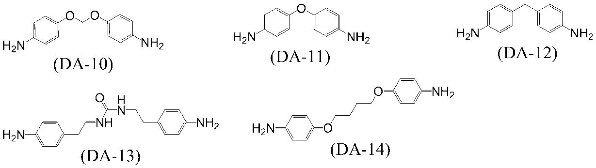
- the diamine component is at least one selected from the following formulas (DA-1) to (DA-20): ⁇ 7.
- step (B) firing is performed at 50 to 150 ° C. ⁇ 8.
- the film is fired at 150 to 300 ° C. ⁇ 9.
- the manufacturing method of the liquid crystal aligning film as described in any one of these.
- the liquid crystal display element which comprises the liquid crystal aligning film of description.
- the liquid crystal display element drives the liquid crystal by a horizontal electric field.
- an afterimage due to long-term alternating current driving that occurs in a liquid crystal display element of an IPS driving method or an FFS driving method can be suppressed, and it occurs when a low molecular weight compound remains.
- a liquid crystal alignment film free from defects can be manufactured with fewer steps than in the past.
- the liquid crystal alignment film obtained by the manufacturing method according to the present invention can be manufactured with a small number of steps, the yield of the liquid crystal display elements can be improved and the liquid crystal display elements can be manufactured more efficiently. It becomes.
- the liquid crystal display element provided with the liquid crystal alignment film obtained by the manufacturing method according to the present invention has excellent afterimage characteristics and reliability, and has a large-screen high-definition liquid crystal television, a small and medium-sized car navigation system, and a smartphone. Etc. can be suitably used.
- a manufacturing method for manufacturing a liquid crystal alignment film according to the present invention is a polyimide (hereinafter referred to as an imidized polyimide precursor) obtained from a tetracarboxylic acid derivative component having a tetracarboxylic acid derivative having a specific structure and a diamine component. , which is also referred to as a specific polymer).
- an imidized polyimide precursor obtained from a tetracarboxylic acid derivative component having a tetracarboxylic acid derivative having a specific structure and a diamine component. , which is also referred to as a specific polymer).
- the specific polymer used in the production method according to the present invention is a polyimide which is an imidized product of a polyimide precursor having a specific structure.
- the polyimide precursor is not particularly limited as long as it is a polyimide precursor that forms an imide ring by heating such as polyamic acid or polyamic acid ester or chemical imidization by a catalyst. From the viewpoint that heating or chemical imidization is likely to proceed, the polyimide precursor is more preferably a polyamic acid or a polyamic acid ester.
- the imidization ratio of polyimide is not particularly limited, but is preferably 10 to 100%, more preferably 50 to 100%, and further preferably 50 to 80%.
- each component used as the raw material which comprises the said specific polymer is explained in full detail.
- the tetracarboxylic acid derivative component used in the polymerization of the specific polymer used in the production method according to the present invention includes not only tetracarboxylic dianhydride but also tetracarboxylic acid and tetracarboxylic acid which are tetracarboxylic acid derivatives thereof.
- a dihalide compound, a tetracarboxylic acid dialkyl ester compound or a tetracarboxylic acid dialkyl ester dihalide compound can also be used.
- the tetracarboxylic dianhydride or its derivative used for the polymerization of the specific polymer is at least one selected from the tetracarboxylic dianhydride and its derivative represented by the following formula (1), and the following formula (2) And at least one selected from tetracarboxylic dianhydrides and derivatives thereof.
- X 1 is a structure represented by the following formulas (X1-1) to (X1-4).
- R 3 to R 6 are each independently a hydrogen atom, a halogen atom, an alkyl group having 1 to 6 carbon atoms, an alkenyl group having 2 to 6 carbon atoms, an alkynyl group having 2 to 6 carbon atoms, or a carbon containing a fluorine atom. These are monovalent organic groups of 1 to 6 or phenyl groups, which may be the same or different, but at least one is other than a hydrogen atom.
- R 7 to R 23 are each independently a hydrogen atom, a halogen atom, an alkyl group having 1 to 6 carbon atoms, an alkenyl group having 2 to 6 carbon atoms, an alkynyl group having 2 to 6 carbon atoms, or a carbon containing a fluorine atom. These are monovalent organic groups having 1 to 6 or phenyl groups, which may be the same or different.
- the structure of X 1 is preferably at least one selected from structures represented by the following formulas (X1-12) to (X1-16). (X1-12) is particularly preferred.
- the proportion of the tetracarboxylic dianhydride represented by the above formula (1) or a derivative thereof is preferably 50 mol% or more, more preferably 70 mol% or more with respect to 1 mol of all tetracarboxylic dianhydrides or derivatives thereof. Preferably, 80 mol% or more is more preferable.
- X 2 is a structure represented by the following formulas (X2-1) to (X2-2).
- the structure of X 2 is preferably a structure represented by the above formula (X2-1).
- the ratio of the tetracarboxylic dianhydride represented by the above formula (2) or a derivative thereof is 1 to 30 mol% with respect to 1 mol of the total tetracarboxylic dianhydride or the derivative thereof (total tetracarboxylic acid derivative component). It is preferably 10 to 30%, more preferably 10 to 20%.
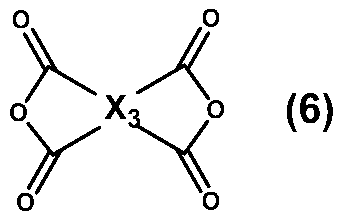
- the tetracarboxylic dianhydride and its derivative used for the polymerization of the specific polymer are the tetracarboxylic dianhydride and its derivative represented by the following formula (6). It may be used.
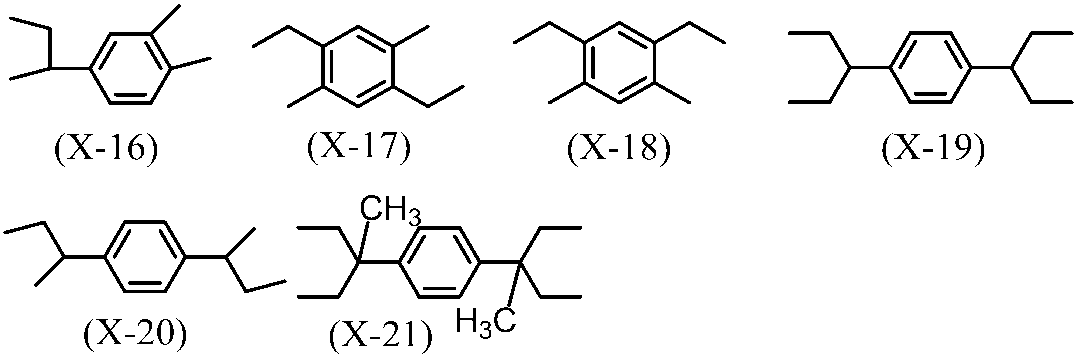
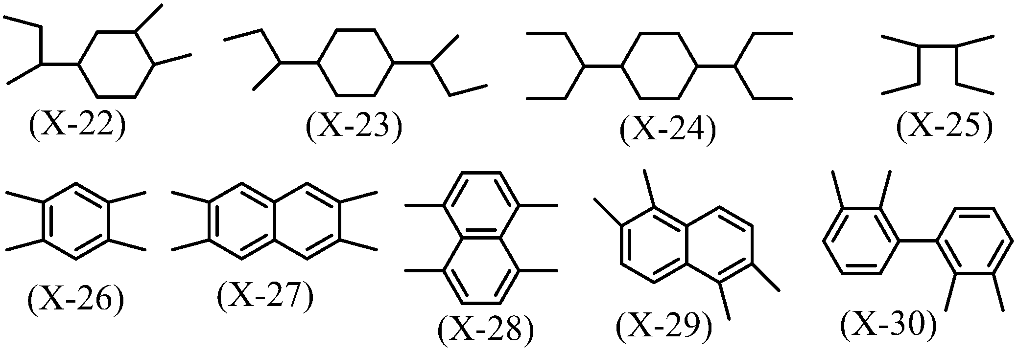
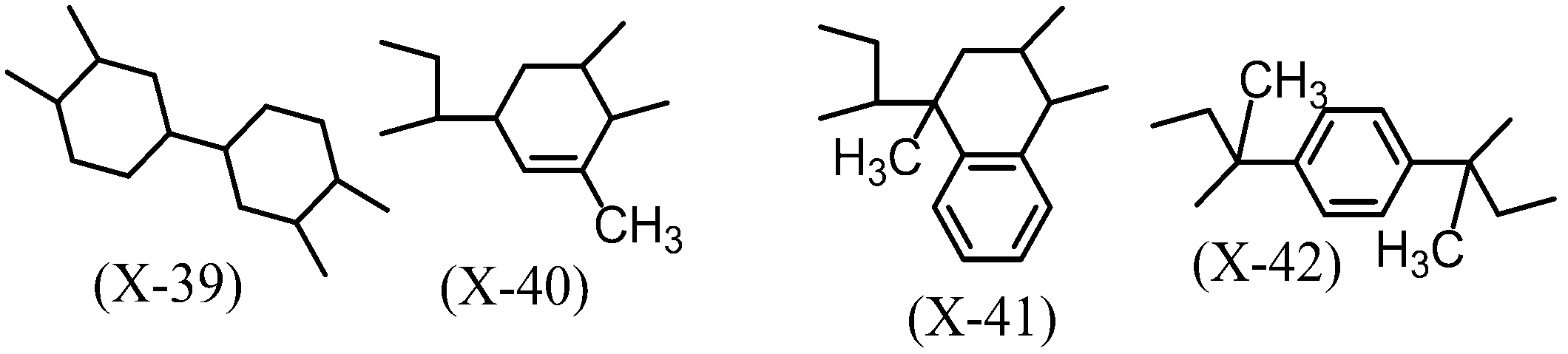
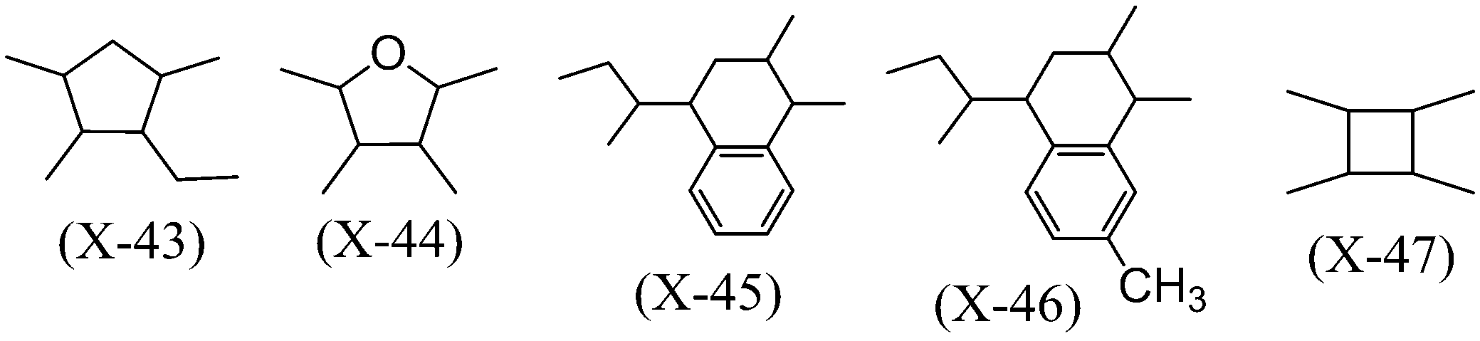
- X 3 is a tetravalent organic group, and its structure is not particularly limited. Specific examples include structures of the following formulas (X-9) to (X-47). From the viewpoint of easy availability of the compound, the structure of X 3 is X-17, X-25, X-26, X-27, X-28, X-32, X-35, X-37, X- 39, X-43, X-44, X-45, X-46, and X-47. Further, from the viewpoint of obtaining a liquid crystal alignment film in which the residual charge accumulated by direct current voltage can be quickly relaxed, it is preferable to use a tetracarboxylic dianhydride having an aromatic ring structure. As the structure of X 3 , X-26 X-27, X-28, X-32, X-35, and X-37 are more preferable.
- the diamine component used for the polymerization of the specific polymer used in the production method according to the present invention is not particularly limited as long as it is a known diamine. From the viewpoint of suppressing afterimages due to long-term alternating current driving, at least one selected from the following formula (3) and the following formula (4) is preferable.
- a 1 is a single bond, an ester bond, an amide bond, a thioester bond, or a divalent organic group having 2 to 20 carbon atoms
- a 2 is a hydrogen atom, a halogen atom, a hydroxyl group, an amino group, a thiol group, a nitro group, A group, a phosphate group, or a monovalent organic group having 1 to 20 carbon atoms
- a is an integer of 1 to 4
- the structures of A 1 may be the same or different.
- b and c are each independently an integer of 1 to 2.
- DA-1, DA-2, DA-4, DA-5, and DA-7 are preferable as the specific structures of the above expressions (3) and (4).
- DA-1, DA-2, DA-4, DA-5, and DA-7 are more preferable.
- the content of the diamine represented by the above formula (3) and the above formula (4) is preferably 50 to 100 mol%, more preferably 70 to 100 mol% with respect to 1 mol of all diamine components.
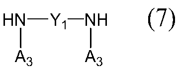
- the diamine used for the polymerization of the specific polymer may include a diamine represented by the following formula (7) in addition to the above formulas (3) and (4).
- a 3 each independently represents a hydrogen atom, an alkyl group having 1 to 5 carbon atoms, an alkenyl group having 2 to 5 carbon atoms, or an alkynyl group having 2 to 5 carbon atoms, which may be the same or different. From the viewpoint of liquid crystal orientation, A 3 is preferably a hydrogen atom or a methyl group.
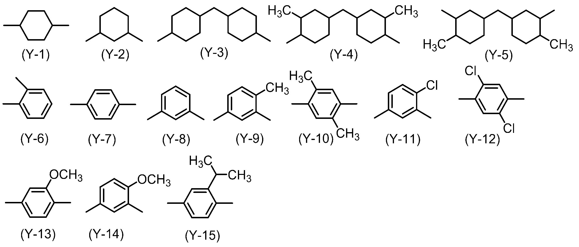
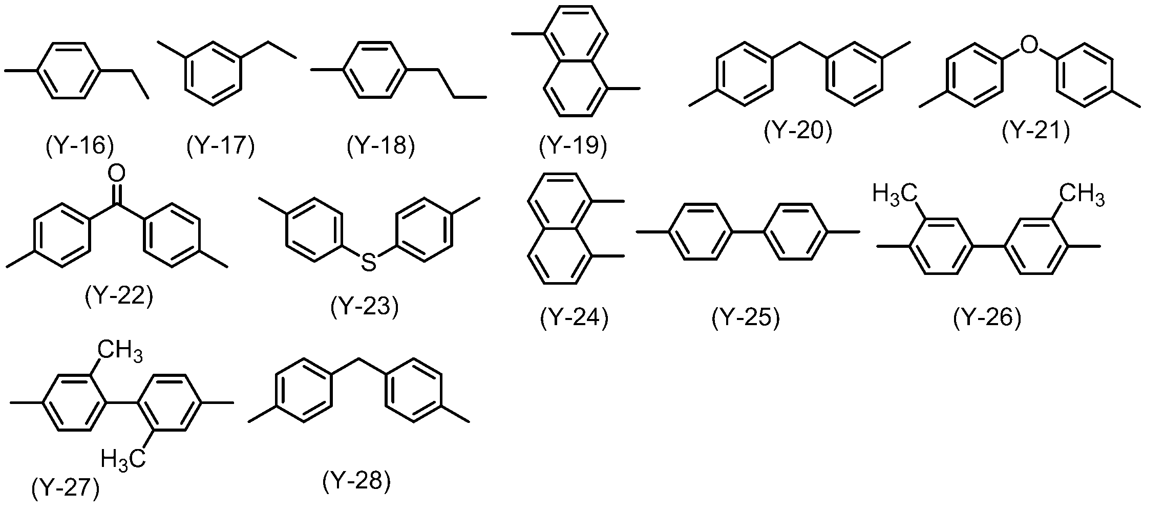
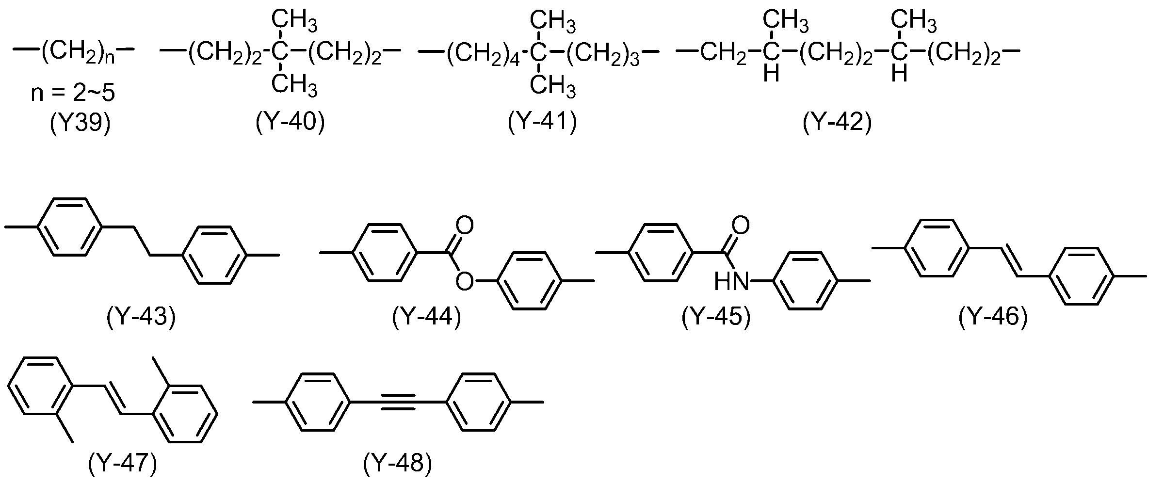
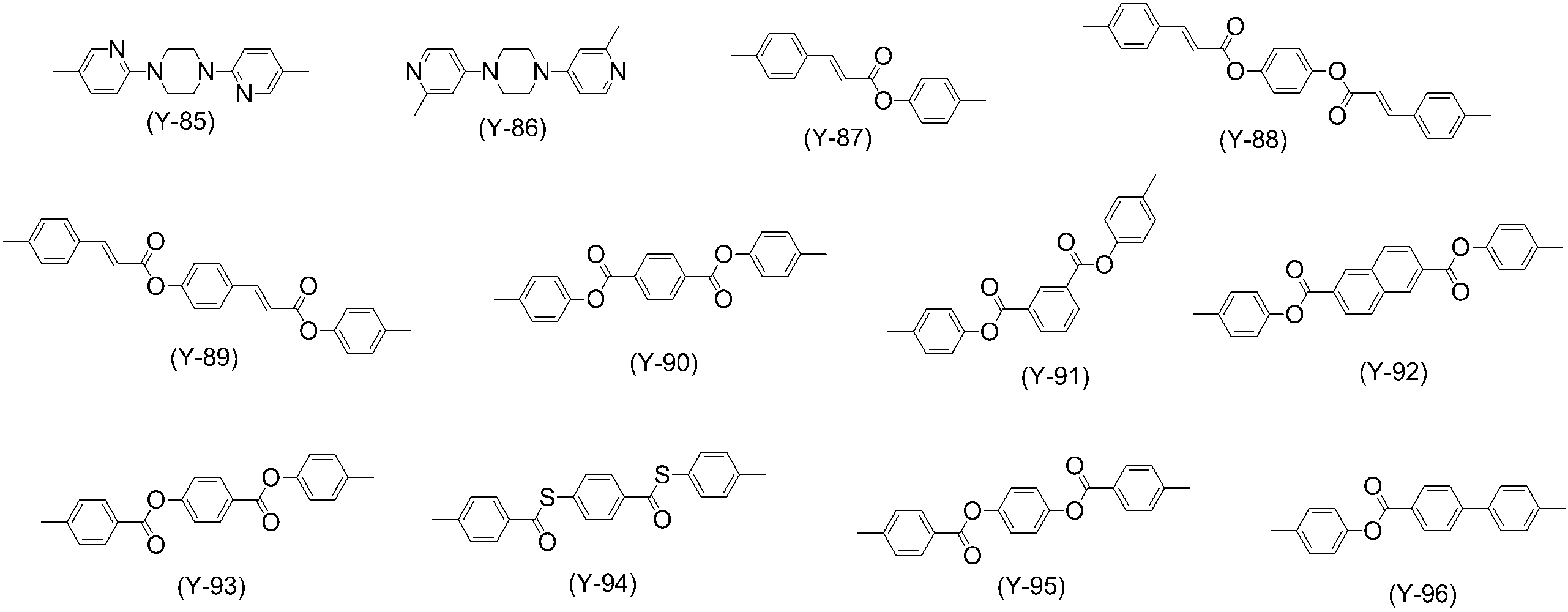
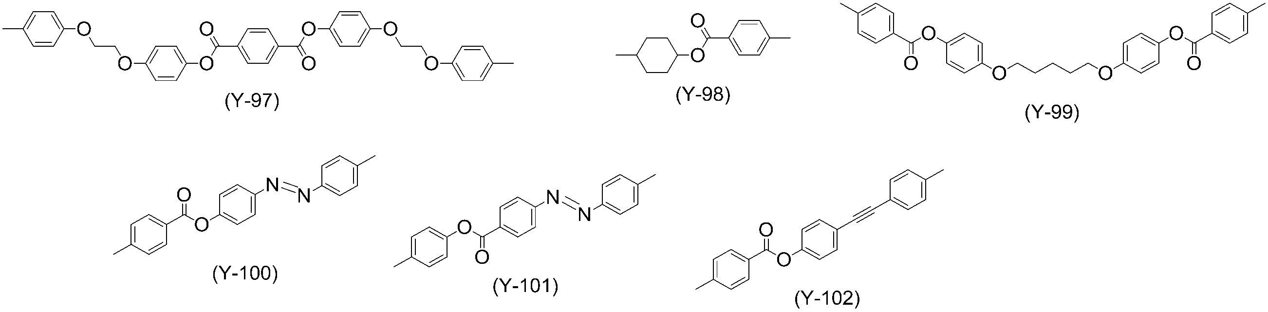
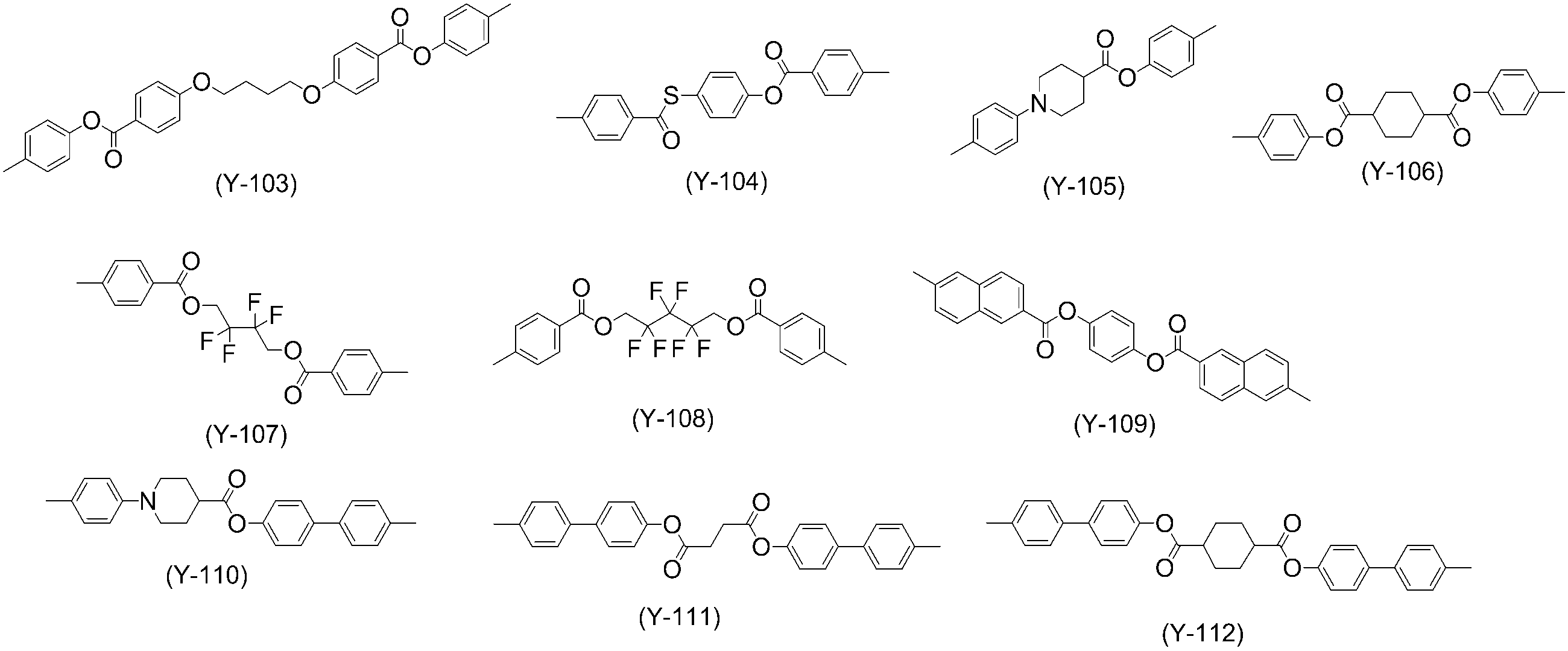
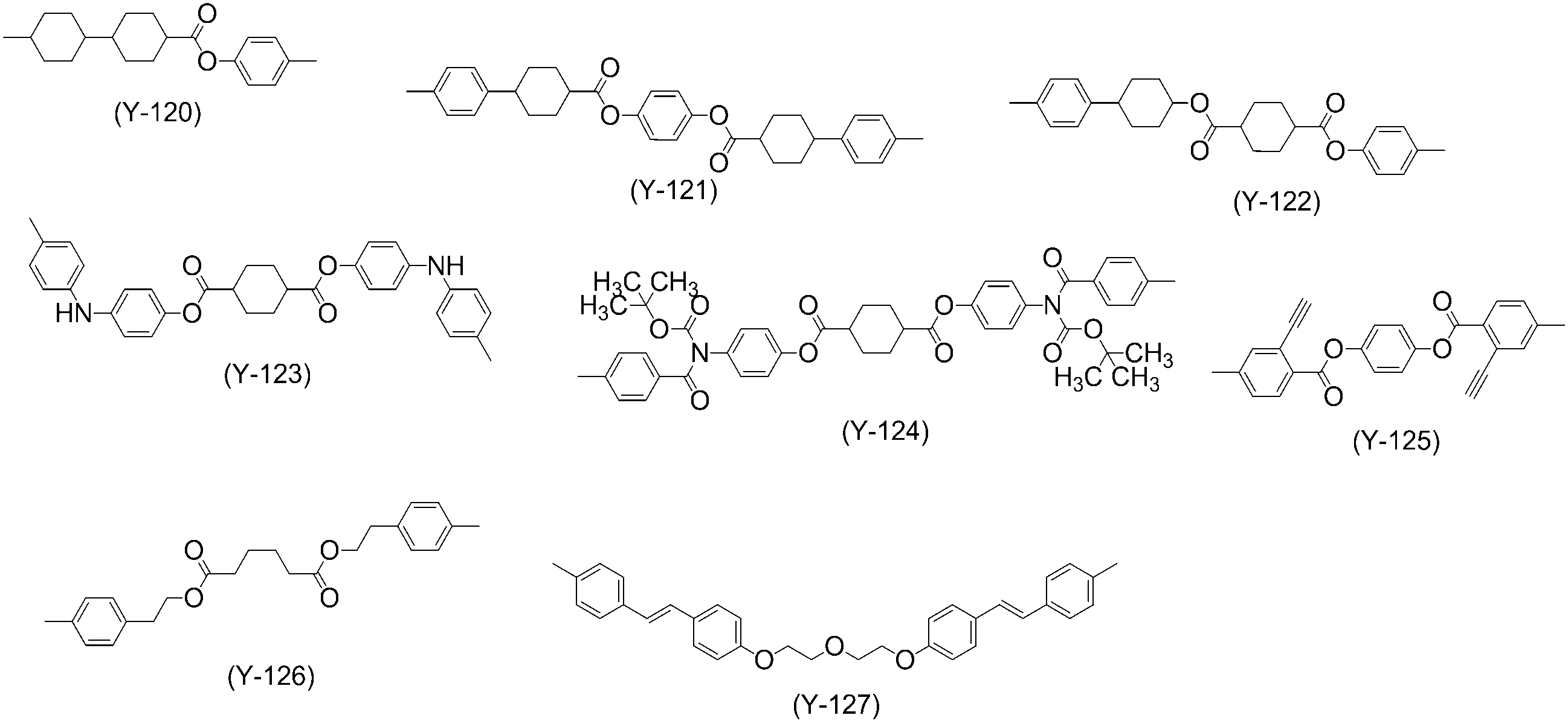
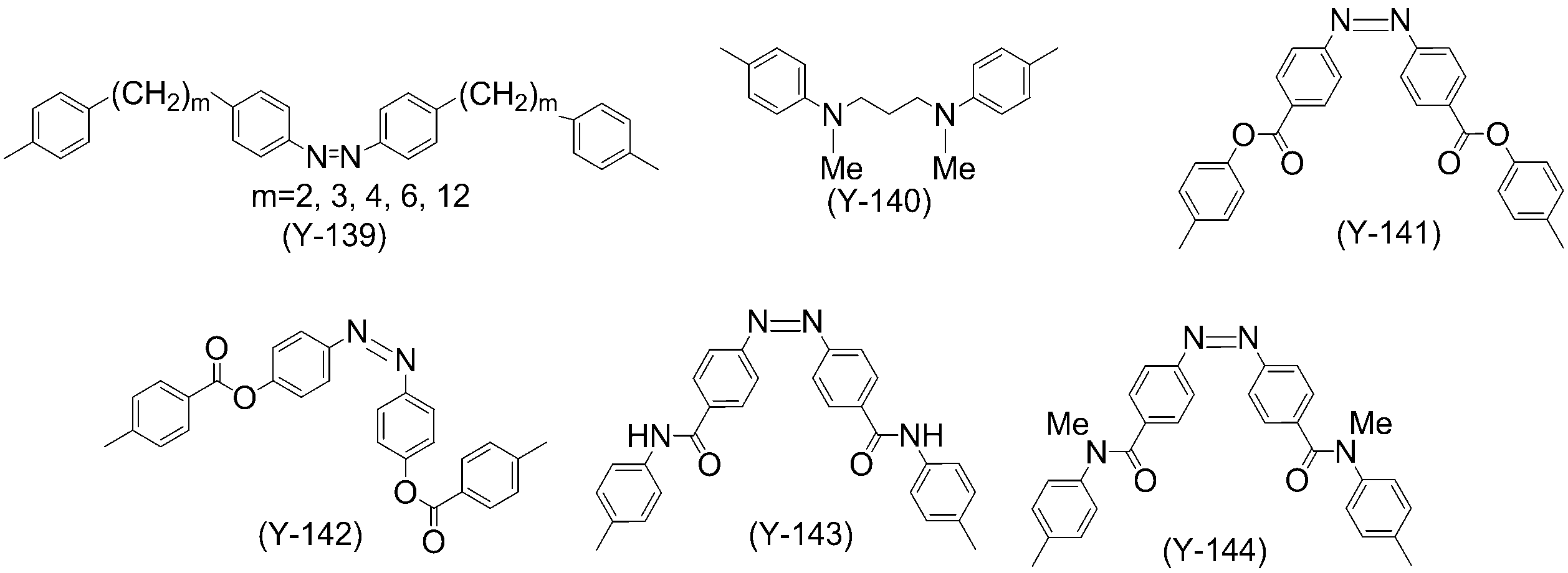
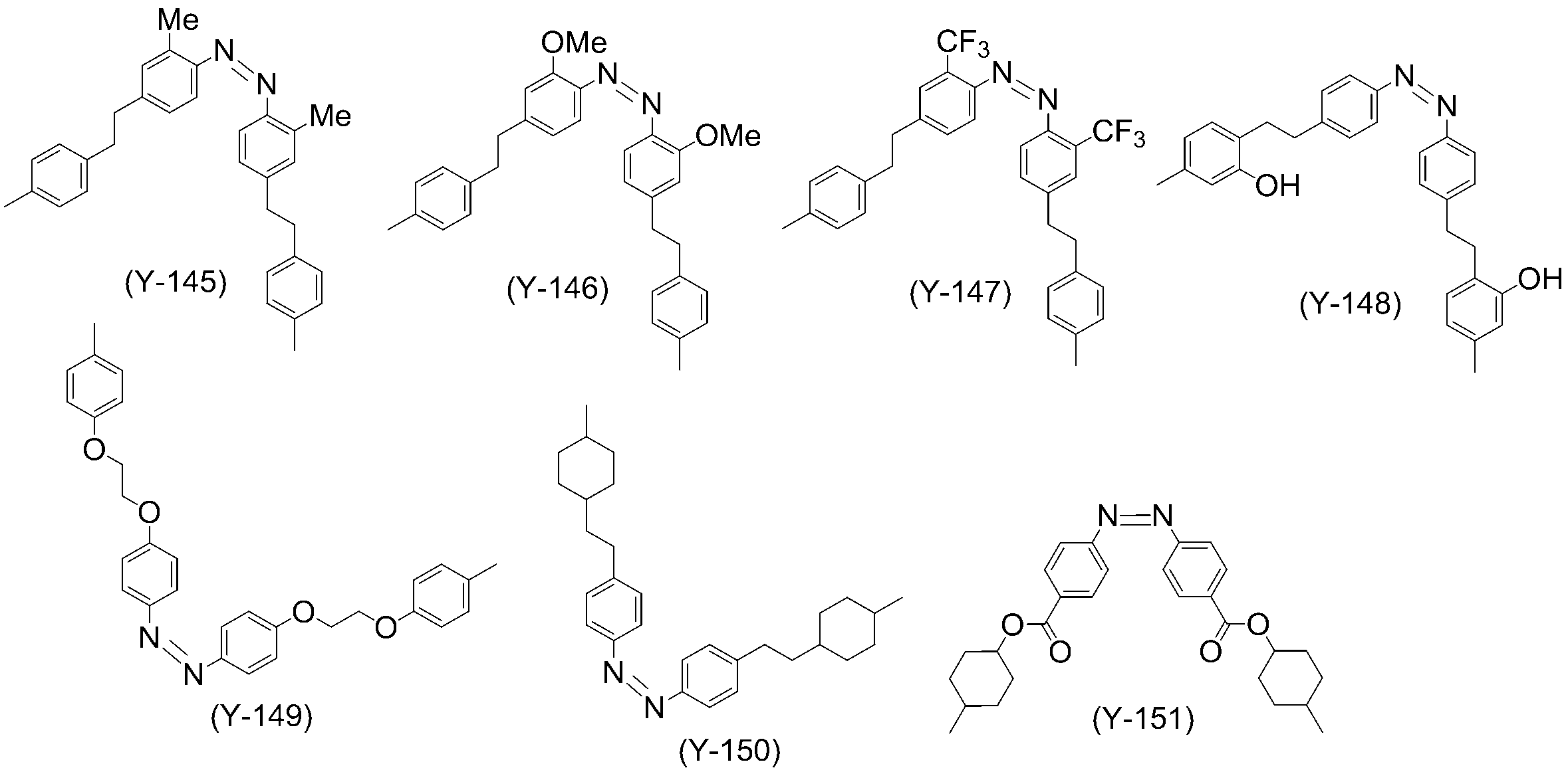
- Y 1 is a divalent organic group, and includes the following formulas (Y-1) to (Y-49) and (Y-57) to (Y-167).
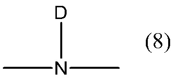
- the structure represented by the following formula (8) is preferably included in the structure of Y 1 .
- D is a t-butoxycarbonyl group.
- Y 1 including the structure represented by the above formula (8) include Y-158, Y-159, Y-160, Y-161, Y-162, and Y-163.
- polyamic acid ester, polyamic acid and polyimide ⁇ Production method of polyamic acid ester, polyamic acid and polyimide>
- the polyamic acid ester, polyamic acid, and polyimide that are polyimide precursors used in the present invention can be synthesized by a known method as described in, for example, International Publication No. WO2013 / 157586.
- the liquid crystal aligning agent used in the present invention has a form of a solution in which a polymer component is dissolved in an organic solvent.
- the molecular weight of the polymer is preferably 2,000 to 500,000 in terms of weight average molecular weight, more preferably 5,000 to 300,000, and still more preferably 10,000 to 100,000.
- the number average molecular weight is preferably 1,000 to 250,000, more preferably 2,500 to 150,000, and still more preferably 5,000 to 50,000.
- the concentration of the polymer of the liquid crystal aligning agent used in the present invention can be appropriately changed by setting the thickness of the coating film to be formed, but it is 1 mass from the point of forming a uniform and defect-free coating film. % From the viewpoint of storage stability of the solution, and preferably 10% by mass or less. A particularly preferred polymer concentration is 2 to 8% by mass.
- the organic solvent contained in the liquid crystal aligning agent used in the present invention is not particularly limited as long as the polymer component is uniformly dissolved.
- Specific examples thereof include N, N-dimethylformamide, N, N-diethylformamide, N, N-dimethylacetamide, N-methyl-2-pyrrolidone, N-ethyl-2-pyrrolidone, N-methylcaprolactam, Examples include 2-pyrrolidone, N-vinyl-2-pyrrolidone, dimethyl sulfoxide, dimethyl sulfone, ⁇ -butyrolactone, 1,3-dimethyl-imidazolidinone, 3-methoxy-N, N-dimethylpropanamide and the like.
- the liquid crystal aligning agent used for this invention may contain the solvent for improving the coating-film uniformity at the time of apply
- a solvent a solvent having a surface tension lower than that of the organic solvent is generally used. Specific examples thereof include ethyl cellosolve, butyl cellosolve, ethyl carbitol, butyl carbitol, ethyl carbitol acetate, ethylene glycol, 1-methoxy-2-propanol, 1-ethoxy-2-propanol, and 1-butoxy-2-propanol.
- liquid crystal aligning agent of the present invention in addition to the above, as long as the effects of the present invention are not impaired, polymers other than the specific polymer, and the electrical properties such as the dielectric constant and conductivity of the liquid crystal aligning film are changed.
- silane coupling agent for the purpose of improving the adhesion between the liquid crystal alignment film and the substrate
- crosslinkable compound for the purpose of increasing the hardness and density of the film when the liquid crystal alignment film is formed
- the production method for producing a liquid crystal alignment film according to the present invention is a method in which the specific polymer is substantially imidated by heat imidization by coating a liquid crystal aligning agent containing the above-mentioned specific polymer on a substrate. Heating under non-advanced conditions, and then proceeding with thermal imidization of the specific polymer, which is carried out in the conventional liquid crystal alignment film manufacturing process, and almost completely evaporating the residual solvent (hereinafter referred to as the baking process) Irradiation with polarized ultraviolet light, and then a firing step is performed.
- the number of manufacturing steps can be reduced, and the liquid crystal display element obtained by including the obtained liquid crystal alignment film can surprisingly suppress afterimages due to long-term AC driving, and low molecular weight compounds remain. There will be no defects such as bright spots.
- a step of applying a liquid crystal aligning agent containing a specific polymer (step (A)), a step of heating the applied liquid crystal aligning agent under conditions in which thermal imidization does not substantially proceed to obtain a film (
- the step (B)) the step of irradiating the film obtained in the step (B) with polarized ultraviolet rays (step (C)), and the step of irradiating the film with ultraviolet rays in the step (C) at 100 ° C. or higher and the step It is characterized by having a step of firing at a temperature higher than (B) (having step (D) and performing step (B) and step (C) successively.
- the substrate on which the liquid crystal aligning agent used in the production method according to the present invention is applied is not particularly limited as long as it is a highly transparent substrate, and a glass substrate, a silicon nitride substrate, and a plastic substrate such as an acrylic substrate or a polycarbonate substrate. Etc. can also be used. At that time, it is preferable to use a substrate on which an ITO electrode or the like for driving the liquid crystal is formed in terms of simplification of the process.
- an opaque material such as a silicon wafer can be used as long as only one substrate is used, and a material that reflects light such as aluminum can be used for the electrode in this case.
- the application method of the liquid crystal aligning agent is not particularly limited, but industrially, a method of screen printing, offset printing, flexographic printing, an ink jet method, or the like is common.
- Other coating methods include a dipping method, a roll coater method, a slit coater method, a spinner method, or a spray method, and these may be used depending on the purpose.
- Step (B) is a step of forming a film by heating the liquid crystal aligning agent applied on the substrate under conditions in which thermal imidization does not substantially proceed.
- the solvent can be evaporated by a heating means such as a hot plate, a thermal circulation oven, or an IR (infrared) oven to form a liquid crystal alignment film.
- a heating means such as a hot plate, a thermal circulation oven, or an IR (infrared) oven to form a liquid crystal alignment film.
- a heating means such as a hot plate, a thermal circulation oven, or an IR (infrared) oven to form a liquid crystal alignment film.
- an arbitrary temperature and time can be selected.
- the temperature is not particularly limited as long as it can remove the organic solvent of the liquid crystal aligning agent, but usually it is preferably heated at 50 to 150 ° C. for 1 to 10 minutes in order to sufficiently remove the contained solvent, and 50 to It is more preferable to heat at 120 ° C. for 1 to 5 minutes.
- Step (C) is a step of irradiating polarized ultraviolet rays to the film obtained in step (B).
- a process (B) and a process (C) are performed continuously.
- the ultraviolet rays it is preferable to use ultraviolet rays having a wavelength of 200 to 400 nm, and more preferable are ultraviolet rays having a wavelength of 200 to 300 nm.
- the substrate coated with the liquid crystal alignment film may be irradiated with ultraviolet rays while being heated at 50 to 250 ° C.
- the radiation dose is preferably 1 to 10,000 mJ / cm 2 . Of these, 100 to 5,000 mJ / cm 2 is preferable.
- the liquid crystal alignment film thus prepared can stably align liquid crystal molecules in a certain direction.
- a higher extinction ratio of polarized ultraviolet rays is preferable because higher anisotropy can be imparted.
- the extinction ratio of linearly polarized ultraviolet light is preferably 10: 1 or more, and more preferably 20: 1 or more.
- Step (D) is a step of baking the film irradiated with ultraviolet rays in step (C). Specifically, it is a step of baking at a temperature of 100 ° C. or higher and higher than the temperature heated in the step (B).
- the firing temperature is not particularly limited as long as it is 100 ° C. or higher and higher than the heating temperature in the step (B), but is preferably 150 to 300 ° C., more preferably 150 to 250 ° C., and further preferably 200 to 250 ° C. .
- the firing time is preferably 5 to 120 minutes, more preferably 5 to 60 minutes, and still more preferably 5 to 30 minutes.
- the thickness of the liquid crystal alignment film after baking is too thin, the reliability of the liquid crystal display element may be lowered, and thus it is preferably 5 to 300 nm, and more preferably 10 to 200 nm. Furthermore, after the step (D), the obtained liquid crystal alignment film can be subjected to a contact treatment using water or a solvent.
- the solvent used for the contact treatment is not particularly limited as long as it is a solvent that dissolves a decomposition product generated from the liquid crystal alignment film by irradiation with ultraviolet rays.
- Specific examples include water, methanol, ethanol, 2-propanol, acetone, methyl ethyl ketone, 1-methoxy-2-propanol, 1-methoxy-2-propanol acetate, butyl cellosolve, ethyl lactate, methyl lactate, diacetone alcohol, 3- Examples thereof include methyl methoxypropionate, ethyl 3-ethoxypropionate, propyl acetate, butyl acetate or cyclohexyl acetate.
- water, 2-propanol, 1-methoxy-2-propanol or ethyl lactate is preferable from the viewpoint of versatility and solvent safety. More preferred is water, 1-methoxy-2-propanol or ethyl lactate.
- the solvent may be used alone or in combination of two or more.
- Examples of the above-described contact treatment that is, treatment for bringing water or a solvent into contact with the liquid crystal alignment film irradiated with polarized ultraviolet rays include immersion treatment and spray treatment (also referred to as spray treatment).
- the treatment time in these treatments is preferably 10 seconds to 1 hour from the viewpoint of efficiently dissolving the decomposition products generated from the liquid crystal alignment film by ultraviolet rays.
- the immersion treatment is preferably performed for 1 minute to 30 minutes.
- the solvent used in the contact treatment may be warmed at normal temperature, but is preferably 10 to 80 ° C. Of these, 20 to 50 ° C. is preferable.
- ultrasonic treatment or the like may be performed as necessary.
- rinsing also referred to as rinsing
- a low boiling point solvent such as water, methanol, ethanol, 2-propanol, acetone, or methyl ethyl ketone
- baking of the liquid crystal alignment film either one of rinsing and firing, or both may be performed.
- the firing temperature is preferably 150 to 300 ° C. Of these, 180 to 250 ° C. is preferable. More preferably, the temperature is 200 to 230 ° C.
- the firing time is preferably 10 seconds to 30 minutes. Among these, 1 to 10 minutes is preferable.
- the liquid crystal alignment film of the present invention is suitable as a liquid crystal alignment film for a horizontal electric field type liquid crystal display element such as an IPS mode or an FFS mode, and is particularly useful as a liquid crystal alignment film for an FFS mode liquid crystal display element.
- the liquid crystal display element is obtained using a liquid crystal cell by preparing a liquid crystal cell by a known method after obtaining a substrate with a liquid crystal alignment film obtained from the liquid crystal aligning agent of the present invention.
- a liquid crystal display element having a passive matrix structure will be described as an example.
- the liquid crystal display element of the active matrix structure in which switching elements, such as TFT (Thin Film Transistor), were provided in each pixel part which comprises image display may be sufficient.
- a transparent glass substrate is prepared, a common electrode is provided on one substrate, and a segment electrode is provided on the other substrate.
- These electrodes can be ITO electrodes, for example, and are patterned so as to display a desired image.
- an insulating film is provided on each substrate so as to cover the common electrode and the segment electrode.
- the insulating film can be, for example, a SiO 2 —TiO 2 film formed by a sol-gel method.
- a liquid crystal alignment film is formed on each substrate, the other substrate is overlapped with one substrate so that the liquid crystal alignment film faces each other, and the periphery is bonded with a sealant.
- a spacer is usually mixed in the sealant, and it is preferable to spray a spacer for controlling the substrate gap on the in-plane portion where no sealant is provided.
- a part of the sealant is provided with an opening that can be filled with liquid crystal from the outside.
- a liquid crystal material is injected into the space surrounded by the two substrates and the sealing agent through the opening provided in the sealing agent, and then the opening is sealed with an adhesive.
- a vacuum injection method may be used, or a method utilizing capillary action in the atmosphere may be used.
- the liquid crystal material either a positive liquid crystal material or a negative liquid crystal material may be used.
- a polarizing plate is installed. Specifically, a pair of polarizing plates is attached to the surfaces of the two substrates opposite to the liquid crystal layer.
- the viscosity of the solution was measured using an E-type viscometer TVE-22H (manufactured by Toki Sangyo Co., Ltd.) at a sample amount of 1.1 ml, cone rotor TE-1 (1 ° 34 ′, R24), and a temperature of 25 ° C.
- the molecular weight was measured by a GPC (room temperature gel permeation chromatography) apparatus, and the number average molecular weight (Mn and weight average molecular weight (Mw)) was calculated as a polyethylene glycol and polyethylene oxide equivalent value.
- GPC apparatus manufactured by Shodex (GPC-101), column: manufactured by Shodex (KD803, series of KD805), column temperature: 50 ° C., eluent: N, N-dimethylformamide (as an additive, lithium bromide-water) Japanese product (LiBr ⁇ H 2 O) 30 mmol / L, phosphoric acid / anhydrous crystal (o-phosphoric acid) 30 mmol / L, tetrahydrofuran (THF) 10 ml / L), flow rate: 1.0 ml / min
- Standard sample for preparing calibration curve TSK standard polyethylene oxide (weight average molecular weight (Mw) about 900,000, 150,000, 100,000, 30,000) manufactured by Tosoh Corporation, and polyethylene glycol (peak top manufactured by Polymer Laboratories) Molecular weight (Mp) about 12,000, 4,000, 1,000).
- Mw weight average molecular weight
- Mp peak top manufactured by Polymer Laboratories
- Mp Molecular weight
- the imidation rate is determined based on protons derived from structures that do not change before and after imidation as reference protons, and the peak integrated value of these protons and proton peaks derived from NH groups of amic acid that appear in the vicinity of 9.5 ppm to 10.0 ppm. It calculated
- equation using the integrated value. Imidization rate (%) (1 ⁇ ⁇ x / y) ⁇ 100
- x is a proton peak integrated value derived from NH group of amic acid
- y is a peak integrated value of reference proton
- ⁇ is one NH group proton of amic acid in the case of polyamic acid (imidation rate is 0%) Is the number ratio of the reference proton to.
- a liquid crystal aligning agent is applied to a 30 mm ⁇ 40 mm ITO substrate by spin coating, dried on a hot plate at 80 ° C. for 2 minutes, and linearly polarized ultraviolet light having a wavelength of 254 nm with an extinction ratio of 10: 1 or more is applied to the coating surface. After the irradiation, the substrate was baked for 30 minutes in a hot air circulation oven at 150 to 230 ° C. to obtain a substrate with a liquid crystal alignment film (polyimide film) having a film thickness of 100 nm.
- a liquid crystal alignment film polyimide film
- Liquid crystal MLC-3019 (manufactured by Merck & Co., Inc.) was injected into this empty cell by a reduced pressure injection method, and the injection port was sealed to obtain a liquid crystal cell.
- the alignment state of the liquid crystal cell produced above was observed with a polarizing microscope (ECLIPSE E600WPOL) (manufactured by Nikon Co., Ltd.).
- a liquid crystal cell having a configuration of a fringe field switching (FFS) mode liquid crystal display element is manufactured.
- a substrate with electrodes was prepared.
- the substrate is a glass substrate having a size of 30 mm ⁇ 50 mm and a thickness of 0.7 mm.
- an ITO electrode having a solid pattern constituting a counter electrode as a first layer is formed.
- a SiN (silicon nitride) film formed by the CVD method is formed as the second layer.
- the second layer SiN film has a thickness of 500 nm and functions as an interlayer insulating film.
- a comb-like pixel electrode formed by patterning an ITO film as the third layer is arranged to form two pixels, a first pixel and a second pixel. ing.
- the size of each pixel is 10 mm long and about 5 mm wide.
- the first-layer counter electrode and the third-layer pixel electrode are electrically insulated by the action of the second-layer SiN film.
- the pixel electrode of the third layer has a comb-like shape configured by arranging a plurality of electrode elements having a dogleg shape whose central portion is bent.
- the width in the short direction of each electrode element is 3 ⁇ m, and the distance between the electrode elements is 6 ⁇ m. Since the pixel electrode forming each pixel is formed by arranging a plurality of bent-shaped electrode elements in the central portion, the shape of each pixel is not rectangular, but in the central portion like the electrode elements. It has a shape that bends and resembles a bold-faced koji.
- Each pixel is divided into upper and lower portions with a central bent portion as a boundary, and has a first region on the upper side of the bent portion and a second region on the lower side.
- the formation directions of the electrode elements of the pixel electrodes constituting them are different. That is, when the rubbing direction of the liquid crystal alignment film described later is used as a reference, the electrode element of the pixel electrode is formed to form an angle of + 10 ° (clockwise) in the first region of the pixel, and the pixel in the second region of the pixel.
- the electrode elements of the electrode are formed so as to form an angle of ⁇ 10 ° (clockwise). That is, in the first region and the second region of each pixel, the directions of the rotation operation (in-plane switching) of the liquid crystal induced by the voltage application between the pixel electrode and the counter electrode are mutually in the substrate plane. It is comprised so that it may become a reverse direction.
- spin coating is applied to the prepared substrate with electrodes and a glass substrate having a columnar spacer having a height of 4 ⁇ m on which an ITO film is formed on the back surface. It was applied by the method. After drying for 2 minutes on a hot plate at 80 ° C. and irradiating the coating surface with UV light having a wavelength of 254 nm, which is linearly polarized with an extinction ratio of 10: 1 or more, through a polarizing plate, then in a hot air circulation oven at 230 ° C. for 30 minutes. Firing was performed to form a coating film having a thickness of 100 nm.
- the two substrates are combined as a set, a sealant is printed on the substrate, and the other substrate is bonded so that the liquid crystal alignment film faces and the alignment direction is 0 °, and then the sealant is added.
- An empty cell was produced by curing.
- Liquid crystal MLC-3019 manufactured by Merck & Co., Inc.
- a liquid crystal cell having the same structure as the liquid crystal cell used for the above-described afterimage evaluation was prepared. Using this liquid crystal cell, an AC voltage of ⁇ 5 V was applied for 120 hours at a frequency of 60 Hz in a constant temperature environment of 60 ° C. Thereafter, the pixel electrode and the counter electrode of the liquid crystal cell were short-circuited and left as it was at room temperature for one day. After leaving, the liquid crystal cell is placed between two polarizing plates arranged so that the polarization axes are orthogonal, and the backlight is turned on with no voltage applied so that the brightness of the transmitted light is minimized. The arrangement angle of the liquid crystal cell was adjusted.
- the rotation angle when the liquid crystal cell was rotated from the angle at which the second region of the first pixel became darkest to the angle at which the first region became darkest was calculated as an angle ⁇ .
- the second region and the first region were compared to calculate a similar angle ⁇ .
- the obtained reaction solution was poured into 427 ml of methanol while stirring, and the deposited precipitate was collected by filtration and subsequently washed with 427 ml of methanol three times.
- the obtained resin powder was dried at 60 ° C. for 12 hours to obtain a polyimide resin powder (A).
- Example 1 Take 1.80 g of the polyimide resin powder (A) obtained in Synthesis Example 21 in a 100 ml Erlenmeyer flask, add 13.2 g of NMP to a solid content concentration of 15%, and stir and dissolve at 70 ° C. for 24 hours. A polyimide solution (A) was obtained. To this polyimide solution, 2.90 g of NMP, 9.00 g of GBL, and 6.00 g of BCS were added and stirred at room temperature for 3 hours to obtain a liquid crystal aligning agent (1). This liquid crystal aligning agent was confirmed to be a uniform solution without any abnormalities such as turbidity and precipitation.
- Examples 2 to 13 and Comparative Examples 1 and 2> A polyimide solution (B) to (O) was obtained in the same manner as in Example 1 except that the polyimide resin powder (B) to (O) was used instead of the polyimide resin powder (A). Were used to obtain liquid crystal aligning agents (2) to (15).
- Example 14 ⁇ Example 14> 4.80 g of the polyimide solution (A) obtained in the same manner as in Example 1 and 7.20 g of the polyamic acid solution (T) obtained in Synthesis Example 20 were placed in a 100 ml Erlenmeyer flask, and 3.00 g of NMP was obtained. And 9.00 g of GBL and 6.00 g of BCS were added and stirred at room temperature for 3 hours to obtain a liquid crystal aligning agent (16). This liquid crystal aligning agent was confirmed to be a uniform solution without any abnormalities such as turbidity and precipitation.
- Example 15 Except for using polyimide resin powder (P) instead of polyimide resin powder (N), a polyimide solution (P) was obtained in the same manner as in Example 14, and a liquid crystal aligning agent (19) was obtained using this. It was. This liquid crystal aligning agent was confirmed to be a uniform solution without any abnormalities such as turbidity and precipitation.
- Example 16 Except for using the polyimide resin powder (Q) instead of the polyimide resin powder (N), a polyimide solution (Q) was obtained in the same manner as in Example 14, and a liquid crystal aligning agent (20) was obtained using this. It was. This liquid crystal aligning agent was confirmed to be a uniform solution without any abnormalities such as turbidity and precipitation.
- Example 17 After the liquid crystal aligning agent (1) obtained in Example 1 was filtered through a 1.0 ⁇ m filter, the liquid crystal aligning agent was applied to a 30 mm ⁇ 40 mm ITO substrate by a spin coating method, and then on an 80 ° C. hot plate. After drying for 2 minutes and irradiating the coated surface with 0.35 J / cm 2 of linearly polarized UV light having an extinction ratio of 26: 1 through a polarizing plate at a wavelength of 254 nm, baking is performed in a hot air circulation oven at 230 ° C. for 30 minutes. And a substrate with a liquid crystal alignment film was obtained.
- Examples 18 to 32, Comparative Examples 5 to 8> instead of the liquid crystal aligning agent (1), the liquid crystal aligning agent shown in Table 3 was used, respectively, and the same as in Example 17 except that the ultraviolet irradiation amount and the baking temperature were those shown in Table 4.
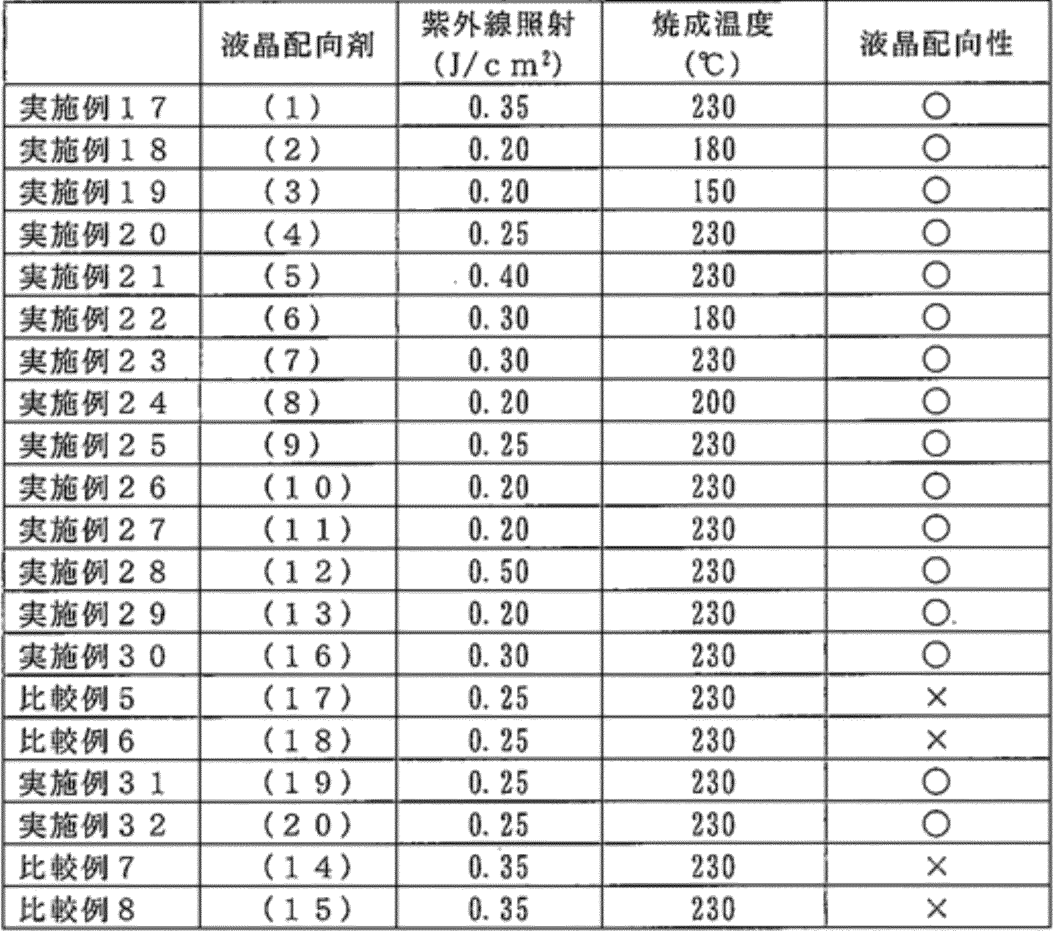
- a liquid crystal cell for liquid crystal alignment evaluation was prepared by the method described above. The evaluation results of the liquid crystal orientation in each are shown in Table 4.
- Example 33 After filtering the liquid crystal aligning agent (1) with a 1.0 ⁇ m filter, the prepared substrate with electrodes and a glass substrate having a columnar spacer with a height of 4 ⁇ m on which an ITO film is formed on the back surface, Application was performed by spin coating. After drying on an 80 ° C. hot plate for 2 minutes, the coating surface was irradiated with 0.35 J / cm 2 of linearly polarized UV light having an extinction ratio of 26: 1 through a polarizing plate at a wavelength of 254 nm, and then circulating hot air at 230 ° C. The substrate was baked in an oven for 30 minutes to obtain a substrate with a liquid crystal alignment film having a thickness of 100 nm.
- the above-mentioned two substrates obtained as a set were printed with a sealant on the substrate, and the other substrate was bonded so that the liquid crystal alignment film faced and the alignment direction was 0 °,
- the agent was cured to produce an empty cell.
- Liquid crystal MLC-3019 manufactured by Merck & Co., Inc.
- the obtained liquid crystal cell was heated at 110 ° C. for 1 hour and left to stand for evaluation of afterimages by long-term AC driving.
- the value of the angle ⁇ of this liquid crystal cell after long-term AC driving was 0.05. Further, as a result of observing the bright spots in the cell, the number of bright spots was less than 10, which was favorable.
- a liquid crystal cell was fabricated and afterimage evaluation was performed by long-term alternating current drive.
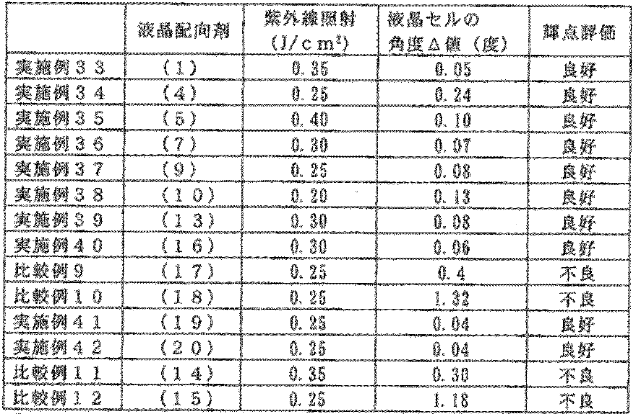
- Table 5 shows the value of the angle ⁇ of the liquid crystal cell and the bright spot evaluation result after long-term AC driving in each case.
- the liquid crystal alignment film obtained by the manufacturing method according to the present invention can be manufactured with a small number of steps, the yield of the liquid crystal display elements can be improved and the liquid crystal display elements can be manufactured more efficiently. Further, by using the liquid crystal alignment film obtained by the manufacturing method according to the present invention, it is possible to suppress the afterimage due to long-term alternating current driving that occurs in the liquid crystal display element of the IPS driving method or the FFS driving method. Furthermore, the liquid crystal alignment film obtained by the production method according to the present invention has a low generation amount of low molecular weight components generated by cutting the main chain of the polyimide, so that it is possible to suppress the occurrence of alignment defects and bright spots, and the higher quality. A liquid crystal display element can be manufactured.
- the liquid crystal display element including the liquid crystal alignment film manufactured by the manufacturing method according to the present invention has excellent afterimage characteristics and reliability, and has a large-screen high-definition liquid crystal television, a small-sized car navigation system, It can be suitably used for a smartphone or the like.
Landscapes
- Chemical & Material Sciences (AREA)
- Physics & Mathematics (AREA)
- Medicinal Chemistry (AREA)
- Health & Medical Sciences (AREA)
- Polymers & Plastics (AREA)
- Organic Chemistry (AREA)
- Chemical Kinetics & Catalysis (AREA)
- Nonlinear Science (AREA)
- Spectroscopy & Molecular Physics (AREA)
- Mathematical Physics (AREA)
- Crystallography & Structural Chemistry (AREA)
- General Physics & Mathematics (AREA)
- Optics & Photonics (AREA)
- Liquid Crystal (AREA)
- Macromolecular Compounds Obtained By Forming Nitrogen-Containing Linkages In General (AREA)
Abstract
Description
工程(A):下記式(1)で表されるテトラカルボン酸二無水物、及びその誘導体から選ばれる少なくとも1種類と、下記式(2)で表されるテトラカルボン酸二無水物、及びその誘導体から選ばれる少なくとも1種類を含有するテトラカルボン酸誘導体成分と、ジアミン成分と、から得られるポリイミド前駆体のイミド化物であるポリイミドを含有する液晶配向剤を塗布する工程。
工程(B):塗布した液晶配向剤を熱イミド化が実質的に進行しない条件で加熱して膜を得る工程。
工程(C):工程(B)で得られた膜に偏光された紫外線を照射する工程。
工程(D):工程(C)で紫外線を照射した膜を、100℃以上、かつ、工程(B)で加熱した温度よりも高い温度で焼成する工程。




本発明に係る製造方法に用いられる特定重合体は、特定構造を有するポリイミド前駆体のイミド化物であるポリイミドである。ポリイミド前駆体としては、ポリアミック酸、ポリアミック酸エステル等の加熱又は触媒による化学イミド化によって、イミド環を形成するポリイミド前駆体であれば、特に限定されない。加熱、又は化学イミド化が進行しやすいという観点から、ポリイミド前駆体としては、ポリアミック酸、又はポリアミック酸エステルがより好ましい。ポリイミドのイミド化率は、特に限定されないが、10~100%が好ましく、50~100%がより好ましく、50~80%がさらに好ましい。以下、上記特定重合体をなす原料となる各成分について詳述する。
本発明に係る製造方法で使用する、特定重合体の重合に用いられるテトラカルボン酸誘導体成分としては、テトラカルボン酸二無水物だけでなく、そのテトラカルボン酸誘導体であるテトラカルボン酸、テトラカルボン酸ジハライド化合物、テトラカルボン酸ジアルキルエステル化合物又はテトラカルボン酸ジアルキルエステルジハライド化合物を用いることもできる。



本発明に係る製造方法で使用する、特定重合体の重合に用いられるジアミン成分は、公知のジアミンであれば特に限定されない。長期交流駆動による残像の抑制の観点から、下記式(3)及び下記式(4)から選ばれる少なくとも1種類であることが好ましい。









本発明に用いられるポリイミド前駆体である、ポリアミック酸エステル、ポリアミック酸及びポリイミドは、例えば、国際公開公報WO2013/157586に記載されるような公知の方法で合成できる。
本発明に用いられる液晶配向剤は、重合体成分が有機溶媒中に溶解された溶液の形態を有する。重合体の分子量は、重量平均分子量で2,000~500,000が好ましく、より好ましくは5,000~300,000であり、さらに好ましくは、10,000~100,000である。また、数平均分子量は、好ましくは、1,000~250,000であり、より好ましくは、2,500~150,000であり、さらに好ましくは、5,000~50,000である。
本発明に係る、液晶配向膜を製造する製造方法は、上述した特定重合体を含有した液晶配向剤を基板に塗布して得られた塗膜を、特定重合体の熱イミド化が実質的に進行しない条件で加熱し、その後、従来の液晶配向膜製造工程において行われている、特定重合体の熱イミド化を進行させ、かつ、残存溶媒をほぼ完全に蒸発させる工程(以後、焼成工程とも称する)を経ずに偏光紫外線照射を行い、その後、焼成工程を行う。
本発明に係る製造方法に用いられる液晶配向剤を、塗布する基板としては、透明性の高い基板であれば特に限定されず、ガラス基板、窒化珪素基板とともに、アクリル基板やポリカーボネート基板等のプラスチック基板等を用いることもできる。その際、液晶を駆動させるためのITO電極等が形成された基板を用いると、プロセスの簡素化の点から好ましい。また、反射型の液晶表示素子では、片側の基板のみにならばシリコンウエハー等の不透明な物でも使用でき、この場合の電極にはアルミニウム等の光を反射する材料も使用できる。
工程(B)は、基板上に塗布した液晶配向剤を、熱イミド化が実質的に進行しない条件で加熱し、膜を形成する工程である。液晶配向剤を基板上に塗布した後は、ホットプレート、熱循環型オーブン又はIR(赤外線)型オーブン等の加熱手段により、溶媒を蒸発させて液晶配向膜とすることができる。この工程では、任意の温度と時間を選択することができる。液晶配向剤の有機溶媒を除去できる温度であれば、特に限定されないが、通常は、含有される溶媒を十分に除去するために50~150℃で1~10分加熱することが好ましく、50~120℃で1~5分加熱することがより好ましい。
工程(C)は、工程(B)で得られた膜に偏光された紫外線を照射する工程である。なお、工程(B)と工程(C)は連続して行われる。紫外線としては、200~400nmの波長を有する紫外線を用いることが好ましく、なかでも、200~300nmの波長を有する紫外線がより好ましい。液晶配向性を改善するために、液晶配向膜が塗膜された基板を50~250℃で加熱しながら、紫外線を照射してもよい。また、前記放射線の照射量は、1~10,000mJ/cm2が好ましい。なかでも、100~5,000mJ/cm2が好ましい。このようにして作製した液晶配向膜は、液晶分子を一定の方向に安定して配向させることができる。偏光された紫外線の消光比が高いほど、より高い異方性が付与できるため、好ましい。具体的には、直線に偏光された紫外線の消光比は、10:1以上が好ましく、20:1以上がより好ましい。
工程(D)は、工程(C)で紫外線を照射した膜を焼成する工程である。具体的には、100℃以上、かつ、工程(B)で加熱した温度よりも高い温度で焼成する工程である。焼成温度は、100℃以上、かつ、工程(B)での加熱温度よりも高ければ、特に限定されないが、150~300℃が好ましく、150~250℃がより好ましく、200~250℃がさらに好ましい。焼成時間は、5~120分が好ましく、より好ましくは5~60分、更に好ましくは、5~30分である。焼成後の液晶配向膜の厚みは、薄すぎると液晶表示素子の信頼性が低下する場合があるので、5~300nmが好ましく、10~200nmがより好ましい。更に、前記工程(D)の後、得られた液晶配向膜を、水や溶媒を用いて、接触処理をすることもできる。
NMP:N-メチル-2-ピロリドン
GBL:γ-ブチロラクトン
BCS:ブチルセロソルブ
DA-1:下記式(DA-1)参照
DA-2:下記式(DA-2)参照
DA-3:下記式(DA-3)参照
DA-4:下記式(DA-4)参照
DA-5:下記式(DA-5)参照
DA-6:下記式(DA-6)参照
DA-7:下記式(DA-7)参照
DA-8:下記式(DA-8)参照
DA-9:下記式(DA-9)参照
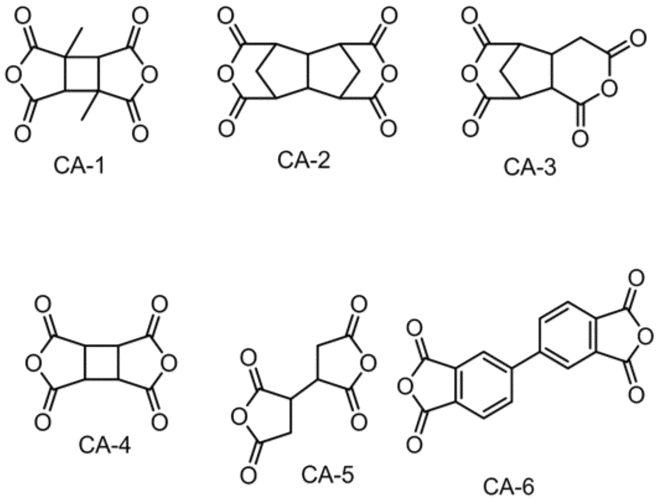
CA-1:下記式(CA-1)参照
CA-2:下記式(CA-2)参照
CA-3:下記式(CA-3)参照
CA-4:下記式(CA-4)参照
CA-5:下記式(CA-5)参照
CA-6:下記式(CA-6)参照


溶液の粘度は、E型粘度計TVE-22H(東機産業社製)を用い、サンプル量1.1ml、コーンロータTE-1(1°34’、R24)、温度25℃で測定した。
分子量は、GPC(常温ゲル浸透クロマトグラフィー)装置によって測定し、ポリエチレングリコール、ポリエチレンオキシド換算値として数平均分子量(Mnと重量平均分子量(Mw)を算出した。
GPC装置:Shodex社製(GPC-101)、カラム:Shodex社製(KD803、KD805の直列)、カラム温度:50℃、溶離液:N,N-ジメチルホルムアミド(添加剤として、臭化リチウム-水和物(LiBr・H2O)が30mmol/L、リン酸・無水結晶(o-リン酸)が30mmol/L、テトラヒドロフラン(THF)が10ml/L)、流速:1.0ml/分
ポリイミド粉末20mgをNMRサンプル管(NMRサンプリングチューブスタンダード,φ5(草野科学社製))に入れ、重水素化ジメチルスルホキシド(DMSO-d6,0.05%TMS(テトラメチルシラン)混合品)(0.53ml)を添加し、超音波をかけて完全に溶解させた。この溶液をNMR測定機(JNW-ECA500)(日本電子データム社製)にて500MHzのプロトンNMRを測定した。イミド化率は、イミド化前後で変化しない構造に由来するプロトンを基準プロトンとして決め、このプロトンのピーク積算値と、9.5ppm~10.0ppm付近に現れるアミド酸のNH基に由来するプロトンピーク積算値とを用い以下の式によって求めた。
イミド化率(%)=(1-α・x/y)×100
30mm×40mmのITO基板に、液晶配向剤をスピンコート法により塗布し、80℃のホットプレート上で2分間乾燥させ、塗膜面に消光比10:1以上の直線偏光した波長254nmの紫外線を照射した後、150~230℃の熱風循環式オーブンで30分間焼成を行い、膜厚100nmの液晶配向膜(ポリイミド膜)付きの基板を得た。上記2枚の基板を一組とし、膜面を内側にして6μmのスペーサーを挟み、基板上にシール剤を印刷し、もう1枚の基板を、液晶配向膜面が向き合い配向方向が0°になるようにして張り合わせた後、シール剤を硬化させて空セルを作製した。この空セルに減圧注入法によって、液晶MLC-3019(メルク株式会社製)を注入し、注入口を封止して、液晶セルを得た。上記で作製した液晶セルの配向状態を偏光顕微鏡(ECLIPSE E600WPOL)(ニコン社製)にて観察し、配向欠陥がないものを「良好」、配向欠陥があるものは「不良」とした。
フリンジフィールドスイッチング(Fringe Field Switching:FFS)モード液晶表示素子の構成を備えた液晶セルを作製する。始めに、電極付きの基板を準備した。基板は、30mm×50mmの大きさで、厚さが0.7mmのガラス基板である。基板上には第1層目として対向電極を構成する、ベタ状のパターンを備えたITO電極が形成されている。第1層目の対向電極の上には第2層目として、CVD法により成膜されたSiN(窒化珪素)膜が形成されている。第2層目のSiN膜の膜厚は500nmであり、層間絶縁膜として機能する。第2層目のSiN膜の上には、第3層目としてITO膜をパターニングして形成された櫛歯状の画素電極が配置され、第1画素及び第2画素の2つの画素を形成している。各画素のサイズは、縦10mmで横約5mmである。このとき、第1層目の対向電極と第3層目の画素電極とは、第2層目のSiN膜の作用により電気的に絶縁されている。
上記した残像評価に使用した液晶セルと同様の構造の液晶セルを準備した。この液晶セルを用い、60℃の恒温環境下、周波数60Hzで±5Vの交流電圧を120時間印加した。その後、液晶セルの画素電極と対向電極との間をショートさせた状態にし、そのまま室温に一日放置した。放置の後、液晶セルを偏光軸が直交するように配置された2枚の偏光板の間に設置し、電圧無印加の状態でバックライトを点灯させておき、透過光の輝度が最も小さくなるように液晶セルの配置角度を調整した。そして、第1画素の第2領域が最も暗くなる角度から第1領域が最も暗くなる角度まで液晶セルを回転させたときの回転角度を角度Δとして算出した。第2画素でも同様に、第2領域と第1領域とを比較し同様の角度Δを算出した。
上記で作製した液晶セルの輝点の評価を行った。液晶セルの輝点の評価は、液晶セルを偏光顕微鏡(ECLIPSE E600WPOL)(ニコン社製)で観察することで行った。具体的には、液晶セルをクロスニコルで設置し、倍率を5倍にした偏光顕微鏡で液晶セルを観察して確認された輝点の数を数え、輝点の数が10個未満を「良好」、輝点の数が10個以上を「不良」とした。
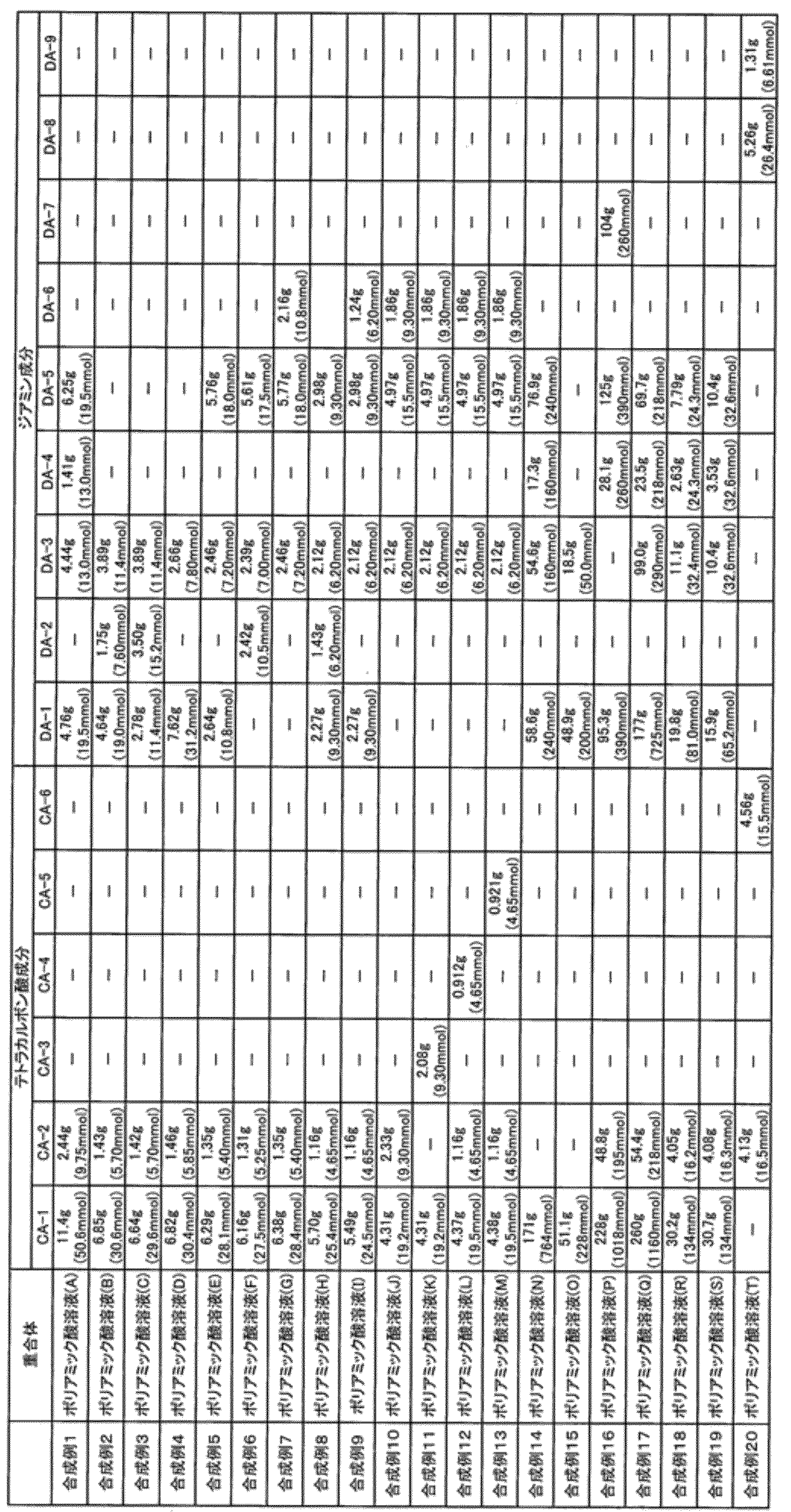
撹拌装置付き及び窒素導入管付きの100ml四つ口フラスコに、DA-1を4.76g(19.5mmol)、DA-3を4.44g(13.0mmol)、DA-4を1.41g(13.0mmol)、DA-5を6.25g(19.5mmol)を取り、NMPを122g加えて、窒素を送りながら撹拌し溶解させた。このジアミン溶液を撹拌しながらCA-1を11.4g(50.6mmol)、CA-2を2.44g(9.75mmol)添加し、更に固形分濃度が15質量%になるようにNMPを52.1g加え、40℃で24時間撹拌してポリアミック酸溶液(A)(粘度:549mPa・s)を得た。ポリアミック酸の分子量は、Mn=11500、Mw=27600であった。
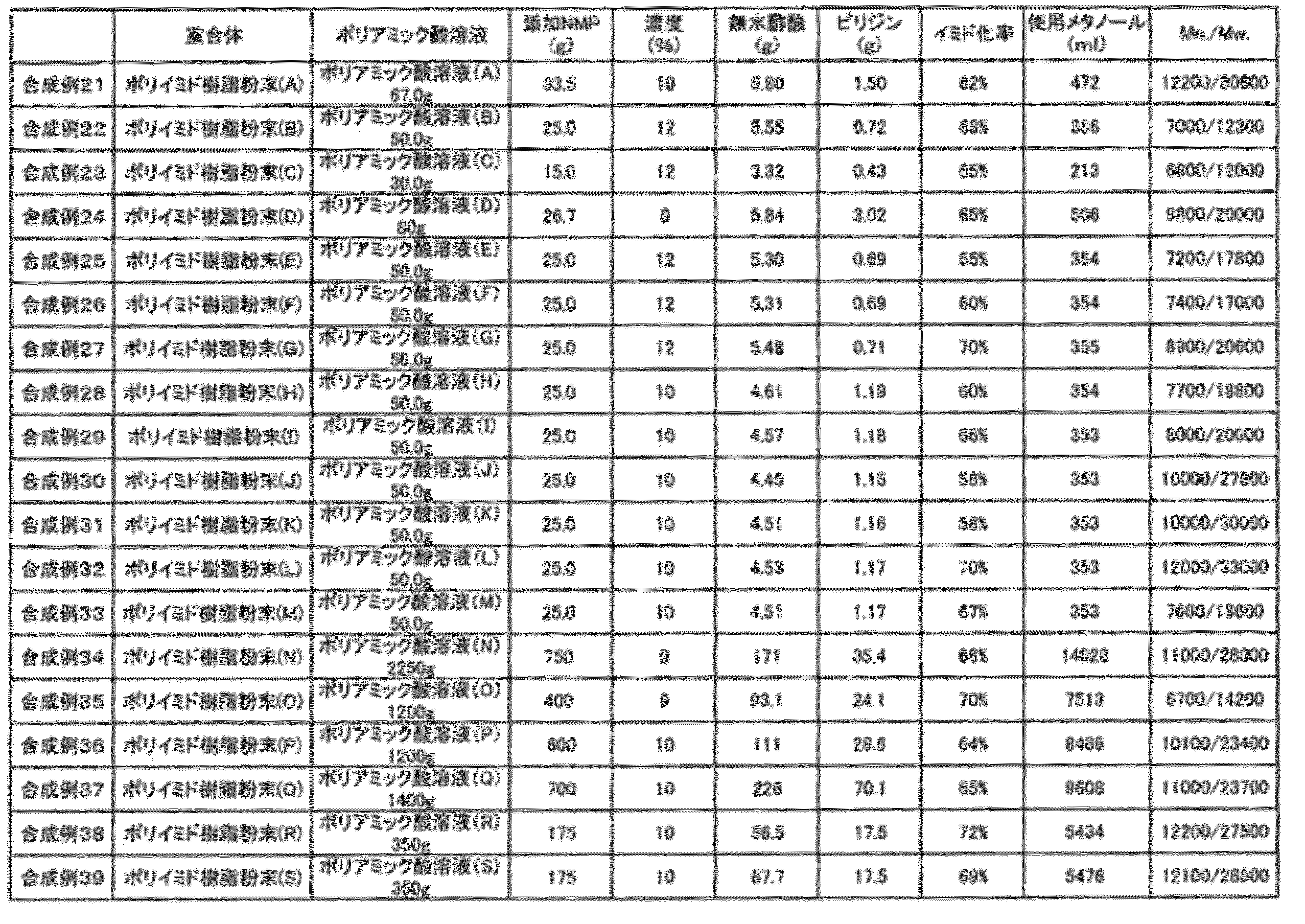
下記表1-1に示す、ジアミン成分、テトラカルボン酸成分を使用し、それぞれ、表1-2に示すNMP量、反応温度、固形分濃度にて、合成例1と同様に実施することにより、ポリアミック酸溶液(B)~(T)を得た。また、得られたポリアミック酸の粘度、及び分子量は、下記表1-2に示す。

撹拌装置付き及び窒素導入管付きの100ml四つ口フラスコに得られたポリアミック酸溶液(A)を67.0g取り、NMPを33.5g加え、30分撹拌した。得られたポリアミック酸溶液に、無水酢酸を5.80g、ピリジンを1.50g加えて、55℃で3時間加熱し、化学イミド化を行った。得られた反応液を427mlのメタノールに撹拌しながら投入し、析出した沈殿物をろ取し、続いて、427mlのメタノールで3回洗浄した。得られた樹脂粉末を60℃で12時間乾燥することで、ポリイミド樹脂粉末(A)を得た。このポリイミド樹脂粉末のイミド化率は62%であり、Mn=12200、Mw=30600であった。
下記表2に示す、ポリアミック酸溶液、NMP、無水酢酸、ピリジン、及びメタノールを使用した以外は、合成例21と同様に実施することにより、下記表2に示すポリイミド樹脂粉末(B)~(S)を得た。
合成例21で得られたポリイミド樹脂粉末(A)1.80gを100ml三角フラスコに取り、固形分濃度が15%になるようにNMPを13.2g加え、70℃で24時間撹拌し溶解させてポリイミド溶液(A)を得た。このポリイミド溶液に、NMPを2.90g、GBLを9.00g、BCSを6.00g添加し、室温で3時間撹拌し、液晶配向剤(1)を得た。この液晶配向剤に、濁りや析出等の異常は見られず、均一な溶液であることが確認された。
ポリイミド樹脂粉末(A)の代わりに、ポリイミド樹脂粉末(B)~(O)を用いた以外は、実施例1と同様に実施することでポリイミド溶液(B)~(O)を得て、これを用いて、液晶配向剤(2)~(15)を得た。
実施例1と同様にして得られたポリイミド溶液(A)4.80gと、合成例20で得られたポリアミック酸溶液(T)7.20gとを、100ml三角フラスコに取り、NMPを3.00g、GBLを9.00g、BCSを6.00g添加し、室温で3時間撹拌し、液晶配向剤(16)を得た。この液晶配向剤に、濁りや析出等の異常は見られず、均一な溶液であることが確認された。
合成例34で得られたポリイミド樹脂粉末(N)1.80gを100ml三角フラスコに取り、固形分濃度が15%になるようにNMPを13.2g加え、70℃で24時間撹拌し溶解させてポリイミド溶液(N)を得た。このポリイミド溶液4.80gと、合成例20で得られたポリアミック酸溶液(T)7.20gとを、100ml三角フラスコに取り、NMPを3.00g、GBLを9.00g、BCSを6.00g添加し、室温で3時間撹拌し、液晶配向剤(17)を得た。この液晶配向剤に、濁りや析出等の異常は見られず、均一な溶液であることが確認された。
ポリイミド樹脂粉末(N)に代えてポリイミド樹脂粉末(O)を用いた以外は、実施例14と同様の操作でポリイミド溶液(O)を得て、これを用いて液晶配向剤(18)を得た。この液晶配向剤に、濁りや析出等の異常は見られず、均一な溶液であることが確認された。
ポリイミド樹脂粉末(N)に代えてポリイミド樹脂粉末(P)を用いた以外は、実施例14と同様の操作でポリイミド溶液(P)を得て、これを用いて液晶配向剤(19)を得た。この液晶配向剤に、濁りや析出等の異常は見られず、均一な溶液であることが確認された。
ポリイミド樹脂粉末(N)に代えてポリイミド樹脂粉末(Q)を用いた以外は、実施例14と同様の操作でポリイミド溶液(Q)を得て、これを用いて液晶配向剤(20)を得た。この液晶配向剤に、濁りや析出等の異常は見られず、均一な溶液であることが確認された。

実施例1で得られた液晶配向剤(1)を1.0μmのフィルターで濾過した後、30mm×40mmのITO基板に、液晶配向剤をスピンコート法により塗布し、80℃のホットプレート上で2分間乾燥させ、塗膜面に偏光板を介して消光比26:1の直線偏光した波長254nmの紫外線を0.35J/cm2照射した後、230℃の熱風循環式オーブンで30分間焼成を行い、液晶配向膜付き基板を得た。得られた上記2枚の基板を一組とし、基板上にシール剤を印刷し、もう1枚の基板を、液晶配向膜面が向き合い配向方向が0°になるようにして張り合わせた後、シール剤を硬化させて空セルを作製した。この空セルに減圧注入法によって、液晶MLC-3019(メルク社製)を注入し、注入口を封止して、液晶配向性液晶セルを得た。液晶の配向状態を確認した結果、配向欠陥がなく、良好であった。
液晶配向剤(1)の代わりに、それぞれ、表3に示した液晶配向剤を用い、また、紫外線の照射量、及び焼成温度を表4に示したものにした以外は、実施例17と同様の方法で液晶配向性評価用液晶セルを作製した。それぞれにおける液晶配向性の評価結果を表4に示す。
上記の液晶配向剤(1)を1.0μmのフィルターで濾過した後、準備された上記電極付き基板と、裏面にITO膜が成膜されている高さ4μmの柱状スペーサーを有するガラス基板に、スピンコート法により塗布にて塗布した。80℃のホットプレート上で2分間乾燥させ、塗膜面に偏光板を介して消光比26:1の直線偏光した波長254nmの紫外線を0.35J/cm2照射した後、230℃の熱風循環式オーブンで30分間焼成を行い、膜厚100nmの液晶配向膜付き基板を得た。得られた上記2枚の基板を一組とし、基板上にシール剤を印刷し、もう1枚の基板を、液晶配向膜面が向き合い配向方向が0°になるようにして張り合わせた後、シール剤を硬化させて空セルを作製した。この空セルに減圧注入法によって、液晶MLC-3019(メルク社製)を注入し、注入口を封止して、FFS駆動液晶セルを得た。その後、得られた液晶セルを110℃で1時間加熱し、一晩放置して、長期交流駆動による残像評価を実施した。長期交流駆動後におけるこの液晶セルの角度Δの値は、0.05であった。また、セル中の輝点観察を行った結果、輝点の数が10個未満であり、良好であった。
液晶配向剤(1)の代わりに、それぞれ、表5に示した液晶配向剤を用い、また、紫外線の照射量を表5に示したものにした以外は、実施例33と同様にしてFFS駆動液晶セルを作製し、長期交流駆動による残像評価を実施した。それぞれにおける長期交流駆動後におけるこの液晶セルの角度Δの値、及び輝点評価結果を表5に示す。
Claims (13)
- 下記(A)、(B)、(C)、及び(D)の工程を有し、かつ工程(B)と工程(C)を連続して行うことを特徴とする液晶配向膜の製造方法。
工程(A):下記式(1)で表されるテトラカルボン酸二無水物、及びその誘導体から選ばれる少なくとも1種類と、下記式(2)で表されるテトラカルボン酸二無水物、及びその誘導体から選ばれる少なくとも1種類と、を含有するテトラカルボン酸誘導体成分と、
ジアミン成分と、から得られるポリイミド前駆体のイミド化物であるポリイミドを含有する液晶配向剤を塗布する工程。
工程(B):塗布した液晶配向剤を熱イミド化が実質的に進行しない条件で加熱して膜を得る工程。
工程(C):工程(B)で得られた膜に偏光された紫外線を照射する工程。
工程(D):工程(C)で紫外線を照射した膜を、100℃以上、かつ、工程(B)で加熱した温度よりも高い温度で焼成する工程。


- 前記工程(A)における、前記ポリイミドのイミド化率が10%~100%であることを特徴とする、請求項1に記載の液晶配向膜の製造方法。
- 前記式(2)で表されるテトラカルボン酸二無水物又はその誘導体を、全テトラカルボン酸誘導体成分1モルに対して、1~30モル%含有することを特徴とする請求項1又は2に記載の液晶配向膜の製造方法。
- 前記式(1)におけるX1の構造が、下記式(X1-12)~(X1-16)で表される構造から選ばれる少なくとも1種であることを特徴とする請求項1~3の何れか一項に記載の液晶配向膜の製造方法。
- 前記式(1)におけるX1の構造が、前記式(X1-12)で表される構造であることを特徴とする請求項1~4の何れか一項に記載の液晶配向膜の製造方法。
- 前記式(2)におけるX2の構造が、前記式(X2-1)で表される構造であることを特徴とする請求項1~5の何れか一項に記載の液晶配向膜の製造方法。
- 前記ジアミン成分が下記式(3)~下記式(4)で表される構造から選ばれる少なくとも1種であることを特徴とする請求項1~6の何れか一項に記載の液晶配向膜の製造方法。
- 前記ジアミン成分が下記式(DA-1)~(DA-20)から選ばれる少なくとも1種であることを特徴とする請求項1~7の何れか一項に記載の液晶配向膜の製造方法。


- 前記工程(B)において、50~150℃で焼成することを特徴とする請求項1~8の何れか一項に記載の液晶配向膜の製造方法。
- 前記工程(D)において、膜を150~300℃で焼成することを特徴とする請求項1~9の何れか一項に記載の液晶配向膜の製造方法。
- 請求項1~10の何れか1項に記載の液晶配向膜の製造方法によって得られることを特徴とする液晶配向膜。
- 請求項11に記載の液晶配向膜を具備することを特徴とする液晶表示素子。
- 前記液晶表示素子が、横電界で液晶を駆動するものであることを特徴とする請求項12に記載の液晶表示素子。
Priority Applications (3)
| Application Number | Priority Date | Filing Date | Title |
|---|---|---|---|
| JP2018558079A JPWO2018117239A1 (ja) | 2016-12-21 | 2017-12-21 | 液晶配向膜の製造方法、液晶配向膜、及び液晶表示素子 |
| KR1020197020591A KR102554524B1 (ko) | 2016-12-21 | 2017-12-21 | 액정 배향막의 제조 방법, 액정 배향막, 및 액정 표시 소자 |
| CN201780087099.5A CN110325903B (zh) | 2016-12-21 | 2017-12-21 | 液晶取向膜的制造方法、液晶取向膜和液晶表示元件 |
Applications Claiming Priority (2)
| Application Number | Priority Date | Filing Date | Title |
|---|---|---|---|
| JP2016-247885 | 2016-12-21 | ||
| JP2016247885 | 2016-12-21 |
Publications (1)
| Publication Number | Publication Date |
|---|---|
| WO2018117239A1 true WO2018117239A1 (ja) | 2018-06-28 |
Family
ID=62626745
Family Applications (1)
| Application Number | Title | Priority Date | Filing Date |
|---|---|---|---|
| PCT/JP2017/046015 Ceased WO2018117239A1 (ja) | 2016-12-21 | 2017-12-21 | 液晶配向膜の製造方法、液晶配向膜、及び液晶表示素子 |
Country Status (5)
| Country | Link |
|---|---|
| JP (1) | JPWO2018117239A1 (ja) |
| KR (1) | KR102554524B1 (ja) |
| CN (1) | CN110325903B (ja) |
| TW (1) | TWI820010B (ja) |
| WO (1) | WO2018117239A1 (ja) |
Cited By (5)
| Publication number | Priority date | Publication date | Assignee | Title |
|---|---|---|---|---|
| WO2020040091A1 (ja) * | 2018-08-20 | 2020-02-27 | 日産化学株式会社 | 液晶配向剤、その製造方法、液晶配向膜、及び液晶表示素子 |
| CN112602013A (zh) * | 2018-08-20 | 2021-04-02 | 日产化学株式会社 | 液晶取向剂、其制造方法、液晶取向膜和液晶表示元件 |
| JP2021140034A (ja) * | 2020-03-05 | 2021-09-16 | 日産化学株式会社 | 液晶配向剤、液晶配向膜及び液晶表示素子 |
| WO2023157876A1 (ja) | 2022-02-17 | 2023-08-24 | 日産化学株式会社 | 液晶配向剤、液晶配向膜、及び液晶表示素子 |
| WO2023224114A1 (ja) | 2022-05-20 | 2023-11-23 | 日産化学株式会社 | 液晶配向剤、液晶配向膜、及び液晶表示素子 |
Citations (3)
| Publication number | Priority date | Publication date | Assignee | Title |
|---|---|---|---|---|
| JP2014219656A (ja) * | 2013-04-09 | 2014-11-20 | Jsr株式会社 | 液晶配向剤 |
| JP2015215462A (ja) * | 2014-05-09 | 2015-12-03 | Jsr株式会社 | 液晶表示素子及びその製造方法 |
| CN106190176A (zh) * | 2015-05-26 | 2016-12-07 | 捷恩智株式会社 | 光取向用液晶取向剂、液晶取向膜及使用其的液晶显示元件及横向电场型液晶显示元件 |
Family Cites Families (14)
| Publication number | Priority date | Publication date | Assignee | Title |
|---|---|---|---|---|
| JP3893659B2 (ja) | 1996-03-05 | 2007-03-14 | 日産化学工業株式会社 | 液晶配向処理方法 |
| CN101007951A (zh) * | 2007-01-18 | 2007-08-01 | 四川大学 | 一种聚酰亚胺液晶垂直取向剂的制备方法 |
| JP5716883B2 (ja) * | 2009-06-09 | 2015-05-13 | Jsr株式会社 | 液晶表示素子の製造方法 |
| JP5654228B2 (ja) | 2009-11-13 | 2015-01-14 | 株式会社ジャパンディスプレイ | 液晶表示装置及び液晶表示装置の製造方法 |
| JP5879693B2 (ja) * | 2011-02-22 | 2016-03-08 | Jsr株式会社 | 液晶配向剤、液晶配向膜及び液晶表示素子 |
| KR102757580B1 (ko) * | 2011-10-27 | 2025-01-21 | 닛산 가가쿠 가부시키가이샤 | 액정 배향제, 액정 배향막 및 액정 표시 소자 |
| KR101986398B1 (ko) * | 2011-12-28 | 2019-06-05 | 닛산 가가쿠 가부시키가이샤 | 액정 배향제, 액정 배향막, 액정 표시 소자 및 액정 표시 소자의 제조 방법 |
| JP5983936B2 (ja) * | 2012-11-19 | 2016-09-06 | Jsr株式会社 | 液晶配向剤 |
| TWI597305B (zh) * | 2012-11-30 | 2017-09-01 | Nissan Chemical Ind Ltd | A method of manufacturing a liquid crystal alignment film, a liquid crystal alignment film, and a liquid crystal display element |
| KR102104154B1 (ko) * | 2012-11-30 | 2020-04-23 | 닛산 가가쿠 가부시키가이샤 | 액정 배향막의 제조 방법, 액정 배향막, 및 액정 표시 소자 |
| KR102168590B1 (ko) * | 2013-03-08 | 2020-10-21 | 닛산 가가쿠 가부시키가이샤 | 액정 배향제, 그들을 사용하여 얻어지는 액정 표시 소자 및 그 제조 방법 |
| KR102103904B1 (ko) * | 2013-04-30 | 2020-04-23 | 엘지디스플레이 주식회사 | 디스플레이 장치 |
| WO2015012316A1 (ja) * | 2013-07-24 | 2015-01-29 | 日産化学工業株式会社 | 液晶配向剤及びそれを用いた液晶配向膜 |
| WO2015060366A1 (ja) * | 2013-10-23 | 2015-04-30 | 日産化学工業株式会社 | 液晶配向剤、液晶配向膜、及び液晶表示素子 |
-
2017
- 2017-12-21 JP JP2018558079A patent/JPWO2018117239A1/ja active Pending
- 2017-12-21 CN CN201780087099.5A patent/CN110325903B/zh active Active
- 2017-12-21 KR KR1020197020591A patent/KR102554524B1/ko active Active
- 2017-12-21 TW TW106145151A patent/TWI820010B/zh active
- 2017-12-21 WO PCT/JP2017/046015 patent/WO2018117239A1/ja not_active Ceased
Patent Citations (3)
| Publication number | Priority date | Publication date | Assignee | Title |
|---|---|---|---|---|
| JP2014219656A (ja) * | 2013-04-09 | 2014-11-20 | Jsr株式会社 | 液晶配向剤 |
| JP2015215462A (ja) * | 2014-05-09 | 2015-12-03 | Jsr株式会社 | 液晶表示素子及びその製造方法 |
| CN106190176A (zh) * | 2015-05-26 | 2016-12-07 | 捷恩智株式会社 | 光取向用液晶取向剂、液晶取向膜及使用其的液晶显示元件及横向电场型液晶显示元件 |
Cited By (13)
| Publication number | Priority date | Publication date | Assignee | Title |
|---|---|---|---|---|
| KR102787959B1 (ko) | 2018-08-20 | 2025-03-27 | 닛산 가가쿠 가부시키가이샤 | 액정 배향제, 그 제조 방법, 액정 배향막, 및 액정 표시 소자 |
| CN112585528A (zh) * | 2018-08-20 | 2021-03-30 | 日产化学株式会社 | 液晶取向剂、其制造方法、液晶取向膜和液晶表示元件 |
| CN112602013A (zh) * | 2018-08-20 | 2021-04-02 | 日产化学株式会社 | 液晶取向剂、其制造方法、液晶取向膜和液晶表示元件 |
| KR20210045393A (ko) | 2018-08-20 | 2021-04-26 | 닛산 가가쿠 가부시키가이샤 | 액정 배향제, 그 제조 방법, 액정 배향막, 및 액정 표시 소자 |
| KR20210045392A (ko) | 2018-08-20 | 2021-04-26 | 닛산 가가쿠 가부시키가이샤 | 액정 배향제, 그 제조 방법, 액정 배향막, 및 액정 표시 소자 |
| JPWO2020040091A1 (ja) * | 2018-08-20 | 2021-08-26 | 日産化学株式会社 | 液晶配向剤、その製造方法、液晶配向膜、及び液晶表示素子 |
| WO2020040091A1 (ja) * | 2018-08-20 | 2020-02-27 | 日産化学株式会社 | 液晶配向剤、その製造方法、液晶配向膜、及び液晶表示素子 |
| CN112585528B (zh) * | 2018-08-20 | 2025-06-20 | 日产化学株式会社 | 液晶取向剂、其制造方法、液晶取向膜和液晶表示元件 |
| JP7375759B2 (ja) | 2018-08-20 | 2023-11-08 | 日産化学株式会社 | 液晶配向剤、その製造方法、液晶配向膜、及び液晶表示素子 |
| JP2021140034A (ja) * | 2020-03-05 | 2021-09-16 | 日産化学株式会社 | 液晶配向剤、液晶配向膜及び液晶表示素子 |
| JP7469736B2 (ja) | 2020-03-05 | 2024-04-17 | 日産化学株式会社 | 液晶配向剤、液晶配向膜及び液晶表示素子 |
| WO2023157876A1 (ja) | 2022-02-17 | 2023-08-24 | 日産化学株式会社 | 液晶配向剤、液晶配向膜、及び液晶表示素子 |
| WO2023224114A1 (ja) | 2022-05-20 | 2023-11-23 | 日産化学株式会社 | 液晶配向剤、液晶配向膜、及び液晶表示素子 |
Also Published As
| Publication number | Publication date |
|---|---|
| TWI820010B (zh) | 2023-11-01 |
| KR102554524B1 (ko) | 2023-07-11 |
| CN110325903A (zh) | 2019-10-11 |
| JPWO2018117239A1 (ja) | 2019-10-31 |
| TW201835657A (zh) | 2018-10-01 |
| KR20190091551A (ko) | 2019-08-06 |
| CN110325903B (zh) | 2023-01-06 |
Similar Documents
| Publication | Publication Date | Title |
|---|---|---|
| JP6627772B2 (ja) | 液晶配向剤、液晶配向膜、及びそれを用いた液晶表示素子 | |
| JP6187457B2 (ja) | 光配向法用の液晶配向剤、液晶配向膜、及び液晶表示素子 | |
| JP7392646B2 (ja) | 液晶配向剤、その製造方法、液晶配向膜、及び液晶表示素子 | |
| JP6202006B2 (ja) | 液晶配向膜の製造方法、液晶配向膜、及び液晶表示素子 | |
| WO2015050135A1 (ja) | 横電界駆動方式用の液晶配向剤、液晶配向膜、及びそれを用いた液晶表示素子 | |
| WO2015050133A1 (ja) | 液晶配向剤、液晶配向膜及びそれを用いた液晶表示素子 | |
| TWI820010B (zh) | 液晶配向膜之製造方法、液晶配向膜及液晶顯示元件 | |
| JP7239872B2 (ja) | 液晶配向剤、液晶配向膜、及び液晶表示素子 | |
| TW202035519A (zh) | 液晶配向劑、液晶配向膜及液晶顯示元件 | |
| WO2019065646A1 (ja) | 液晶配向剤、液晶配向膜及びそれを用いた液晶表示素子 | |
| JP7193783B2 (ja) | 液晶配向剤、液晶配向膜、及びそれを用いた液晶表示素子 | |
| JP2019101196A (ja) | 液晶配向剤、液晶配向膜、及び液晶表示素子 | |
| JP7375759B2 (ja) | 液晶配向剤、その製造方法、液晶配向膜、及び液晶表示素子 | |
| JP2018040979A (ja) | 液晶配向膜の製造方法、液晶配向膜、及び液晶表示素子 | |
| WO2018051923A1 (ja) | 液晶配向剤、液晶配向膜及び液晶表示素子 | |
| JP2019101195A (ja) | 液晶配向膜の製造方法、液晶配向膜、及び液晶表示素子 |
Legal Events
| Date | Code | Title | Description |
|---|---|---|---|
| 121 | Ep: the epo has been informed by wipo that ep was designated in this application |
Ref document number: 17884829 Country of ref document: EP Kind code of ref document: A1 |
|
| ENP | Entry into the national phase |
Ref document number: 2018558079 Country of ref document: JP Kind code of ref document: A |
|
| NENP | Non-entry into the national phase |
Ref country code: DE |
|
| ENP | Entry into the national phase |
Ref document number: 20197020591 Country of ref document: KR Kind code of ref document: A |
|
| 122 | Ep: pct application non-entry in european phase |
Ref document number: 17884829 Country of ref document: EP Kind code of ref document: A1 |