WO2018096830A1 - 電子部品及びその製造方法 - Google Patents
電子部品及びその製造方法 Download PDFInfo
- Publication number
- WO2018096830A1 WO2018096830A1 PCT/JP2017/037019 JP2017037019W WO2018096830A1 WO 2018096830 A1 WO2018096830 A1 WO 2018096830A1 JP 2017037019 W JP2017037019 W JP 2017037019W WO 2018096830 A1 WO2018096830 A1 WO 2018096830A1
- Authority
- WO
- WIPO (PCT)
- Prior art keywords
- electronic component
- resin
- adhesive layer
- sensitive adhesive
- pressure
- Prior art date
- Legal status (The legal status is an assumption and is not a legal conclusion. Google has not performed a legal analysis and makes no representation as to the accuracy of the status listed.)
- Ceased
Links
Images


Classifications
-
- H—ELECTRICITY
- H10—SEMICONDUCTOR DEVICES; ELECTRIC SOLID-STATE DEVICES NOT OTHERWISE PROVIDED FOR
- H10W—GENERIC PACKAGES, INTERCONNECTIONS, CONNECTORS OR OTHER CONSTRUCTIONAL DETAILS OF DEVICES COVERED BY CLASS H10
- H10W70/00—Package substrates; Interposers; Redistribution layers [RDL]
- H10W70/60—Insulating or insulated package substrates; Interposers; Redistribution layers
Definitions
- the present invention relates to an electronic component in which an electronic component element is built in a resin structure and a method for manufacturing the same.
- a component built-in type electronic component in which an electronic component element is built in a resin structure is known.
- a semiconductor chip is mounted on a base material.
- a resin material is applied so as to embed the semiconductor chip.
- This resin material is cured to form a resin structure.
- the base material is isolated.
- an electronic component in which a semiconductor chip is built in the resin structure is obtained.
- the portion of the semiconductor chip that has been in contact with the base material is exposed on the surface.
- the electronic component element and the thermosetting resin are placed in the mold. Fill and press. Then, the thermosetting resin is cured by heating to obtain a resin structure.
- the electronic component element may be misaligned due to the pressure during pressing or the curing shrinkage during heat curing.
- An object of the present invention is to provide a method for manufacturing an electronic component in which the positional deviation of an electronic component element incorporated in a resin structure is unlikely to occur, and an electronic component in which the positional accuracy of the electronic component element is enhanced.
- the method of manufacturing an electronic component according to the present invention includes a step of forming an adhesive layer on a metal sheet, a step of stacking and temporarily fixing electronic component elements on the adhesive layer, and the temporary fixing.
- a resin material is placed in the mold so as to embed the electronic component element and pressed to apply the resin material onto the metal sheet, and the resin material is cured to obtain a resin structure.
- And forming the electronic sheet by removing the metal sheet and the pressure-sensitive adhesive layer.
- the step of removing the pressure-sensitive adhesive layer in at least a part of the region other than the region below the electronic component element before applying the resin material is provided. Furthermore, it is provided. In this case, the resin material contacts the metal sheet in the region where the pressure-sensitive adhesive layer is removed. Therefore, the position shift of the electronic component element during resin curing can be further effectively suppressed.
- the pressure-sensitive adhesive layer in removing at least a part of the pressure-sensitive adhesive layer, is removed in all regions other than the region below the electronic component element. To do. In this case, the displacement of the electronic component element can be more effectively suppressed.
- the method further includes a step of providing a columnar electrode on the metal sheet prior to the formation of the pressure-sensitive adhesive layer, and the columnar electrode is the resin. After sealing the material, it becomes a through electrode penetrating the resin structure.
- the resin structure is connected to the electronic component element, and the resin structure
- the method further includes the step of providing a wiring reaching the outer surface of the body.
- a support plate is provided that is laminated on a surface of the metal sheet opposite to the side on which the pressure-sensitive adhesive layer is provided,
- the pressure-sensitive adhesive layer is formed on the metal sheet supported by a support plate.
- the support plate is made of one material selected from the group consisting of resin, metal, and silicon.
- An electronic component according to the present invention is embedded in a resin structure having a first surface and a second surface facing each other, and is exposed to the first surface of the resin structure.
- An electronic component element, and a wiring provided on the first surface of the resin structure and connected to the electronic component element, the first surface side of the electronic component element There is a step between the first surface of the resin structure and the first surface of the resin structure, and the surface on the first surface side of the electronic component element is more inside the resin structure than the first surface. It is in.
- a through electrode penetrating the first surface and the second surface of the resin structure is further provided.
- the position of the electronic component element embedded in the resin structure is unlikely to occur.
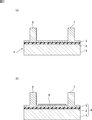
- FIG. 1A and FIG. 1B are front cross-sectional views for explaining a method for manufacturing an electronic component according to the first embodiment of the present invention.
- FIG. 2A and FIG. 2B are front sectional views for explaining a method for manufacturing an electronic component according to the first embodiment of the present invention.
- FIG. 3A and FIG. 3B are front sectional views for explaining a method for manufacturing an electronic component according to the first embodiment of the present invention.
- FIG. 4A and FIG. 4B are front sectional views for explaining a method for manufacturing an electronic component according to the first embodiment of the present invention.
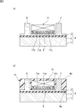
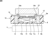
- FIG. 5 is a front sectional view showing the electronic component obtained by the electronic component manufacturing method according to the first embodiment.
- FIG. 6B are front sectional views for explaining a method for manufacturing an electronic component according to the second embodiment of the present invention.
- FIG. 7A and FIG. 7B are front sectional views for explaining a method for manufacturing an electronic component according to the second embodiment of the present invention.
- FIG. 8A and FIG. 8B are front sectional views for explaining a method for manufacturing an electronic component according to the second embodiment of the present invention.
- FIG. 9 is a front sectional view showing an electronic component obtained by the electronic component manufacturing method according to the second embodiment of the present invention.
- FIG. 10 is a front sectional view of an electronic component according to the third embodiment of the present invention.
- a metal sheet 3 is laminated via an adhesive 2 on a support plate 1 made of one material selected from the group consisting of resin, metal, ceramics, and silicon.
- the metal sheet 3 is made of a metal foil in the present embodiment, but may be a metal plate. It does not specifically limit as a metal of the metal sheet 3, Cu, Al, etc. can be used.
- the adhesive 2 may be an adhesive such as glass epoxy resin, or a double-sided adhesive tape.
- a resist pattern 5 shown in FIG. 1B is formed.
- the resist pattern 5 has through holes 5a and 5b.
- the through electrodes 6 and 7 are formed by electroplating. That is, a plating film is grown on the metal sheet 3 by electroplating. Thereby, a columnar electrode is formed.
- the columnar electrodes correspond to through electrodes 6 and 7 that finally penetrate the resin structure, as will be described later.
- the columnar electrodes are also expressed as through electrodes 6 and 7 in the stage of FIG.
- an appropriate metal such as Cu or an alloy can be used.
- the resist pattern 5 is peeled off.
- the through electrodes 6 and 7 are obtained in a state of protruding upward.
- an adhesive layer 8 is provided in a region where the electronic component element is disposed.
- the pressure-sensitive adhesive layer 8 is formed on the entire surface of the metal sheet 3 and then patterned.
- an adhesive may be applied after a mask having an opening in a region where an electronic component element is to be arranged is arranged.
- the material of the pressure-sensitive adhesive layer 8 is not particularly limited, but in this embodiment, a pressure-sensitive adhesive that can be removed by exposure to light and development is used.
- the electronic component element 11 is attached on the pressure-sensitive adhesive layer 8. Although details of the electronic component element 11 are omitted, in the present embodiment, the electronic component element 11 has a resin layer 11a on the surface in contact with the pressure-sensitive adhesive layer 8. Terminals 11b and 11c are provided so as to penetrate the resin layer 11a. The terminals 11b and 11c are electrically connected to functional electrodes and the like in the electronic component element 11.
- the structure shown in FIG. 3A is placed in the mold, and a resin material is applied so that the electronic component element 11 is embedded.
- a resin material such as an epoxy resin is used.
- the resin material is cured by heating while pressing.
- the resin structure 9 shown in FIG. 3B is formed.
- the resin structure 9 has a first surface 9a and a second surface 9b that face each other.
- the electronic component element 11 is sealed with a resin structure 9.
- the first surface 9 a of the resin structure 9 is in close contact with the upper surface of the metal sheet 3.
- the stress due to pressing is transmitted to the electronic component element 11 through the resin material. Further, stress due to curing shrinkage during heat curing is also applied to the electronic component element 11.
- the electronic component element 11 is bonded to the metal sheet 3 by the adhesive layer 8.
- the metal sheet 3 has a relatively high rigidity and is supported by the support plate 1. Therefore, even if the stress as described above is applied, it is difficult for the electronic component element 11 to be displaced.
- the metal sheet 3 is dissolved by etching, and the laminate 4 is removed. Further, the pressure-sensitive adhesive layer 8 made of a photoresist is removed by light exposure and development. In this way, the structure shown in FIG. 4A is obtained.
- a step 12 is provided between the lower surface of the electronic component element 11, that is, the outer surface of the resin layer 11a, and the first surface 9a of the resin structure 9.
- the outer surface of the resin layer 11a is located on the inner side of the resin structure 9 with respect to the first surface 9a. Therefore, a recess 13 is provided.
- wirings 14 and 15 are provided on the first surface 9 a of the resin structure 9.
- the wiring 14 is connected to the through electrode 6 on the first surface 9 a of the resin structure 9.
- the wiring 14 reaches the outer surface of the resin layer 11a, that is, the outer surface, and is electrically connected to the terminal 11b.
- the wiring 15 also extends from the first surface 9a of the resin structure 9 to the outer surface of the resin layer 11a.
- the wiring 15 electrically connects the through electrode 7 and the terminal 11c.
- the wirings 14 and 15 may be stacked not only in one layer but also in a plurality of layers. In the case where a plurality of layers are stacked, an insulating layer is formed between the layers.
- the positional accuracy of the electronic component element 11 in the resin structure 9 is sufficiently high.
- the electronic component 18 has metal bumps 19a and 19b.
- the metal bumps 19 a and 19 b are connected to the wirings 14 and 15.
- another electronic component may be arranged on the lower surface side of the electronic component 16 and electrically connected to the through electrodes 6 and 7. That is, the electronic component 16 can be suitably used as an interposer that electrically connects a plurality of electronic components.
- the electronic component element 11 is not particularly limited, and may be any passive component such as an acoustic wave element or a capacitor, or an active component such as a semiconductor element.
- Other electronic components 18 are not particularly limited.
- another electronic component may be laminated on the lower end side of the through electrodes 6 and 7. That is, the electronic component 16 may be used as an interposer that electrically connects the electronic component indicated by the broken line X and the electronic component 18.
- a laminated body 4 having a support plate 1, an adhesive material 2, and a metal sheet 3 is prepared as in the case of the first embodiment.
- an adhesive layer 21 is provided on the entire surface of the metal sheet 3.
- a pressure-sensitive adhesive photoresist can be used in the same manner as the pressure-sensitive adhesive layer 8.
- the pressure-sensitive adhesive layer 21 can be formed of an appropriate material that can be patterned and removed in a later step.
- the electronic component element 11 is bonded onto the adhesive layer 21.
- the electronic component element 11 As a mask, light is irradiated from above, and a part of the pressure-sensitive adhesive layer 21 is removed by exposure and development.
- the pressure-sensitive adhesive layer 21 in the remaining region excluding the region below the electronic component element 11 is removed. Therefore, as shown in FIG. 7A, the pressure-sensitive adhesive layer 21 remains only below the electronic component element 11.
- the electronic component element 11 is joined to the metal sheet 3 by the adhesive layer 21.
- the structure obtained in the mold is disposed, and the electronic component element 11 is sealed using a resin material made of a thermosetting resin. To be buried. Then, the resin material is cured by heating while pressing. In this way, the resin structure 9 shown in FIG. 7B is formed.
- the first surface 9a of the resin structure 9 and the lower surface of the pressure-sensitive adhesive layer 21, that is, the outer surface are flush with each other.
- the lower surface of the resin layer 11a, that is, the outer surface recedes to the inner side of the resin structure 9 from the first surface 9a. That is, as in the case of the first embodiment, the step 12 is provided between the outer surface of the resin layer 11a and the first surface 9a.
- the resin structure 9 is formed on the pressure-sensitive adhesive layer 21 in a state where the electronic component element 11 is bonded to the metal sheet 3. Accordingly, even if pressure due to pressing or stress due to curing shrinkage during thermal curing is applied to the electronic component element 11, it is difficult for the electronic component element 11 to be displaced.
- the support plate is made of resin, the support plate has elasticity. Therefore, when peeling at the interface between the adhesive 2 and the metal sheet 3, the support plate is elastically deformed to facilitate peeling.
- FIG. 8A the structure shown in FIG. 8A is obtained. Thereafter, the metal sheet 3 is removed by etching, and the pressure-sensitive adhesive layer 21 is dissolved and removed with a solvent. In this way, the structure shown in FIG. 8B is obtained.
- wirings 22 and 23 are provided.
- the wirings 22 and 23 extend from the first surface 9 a of the resin structure 9 to the outer surface of the resin layer 11 a via the step 12.
- the wiring 22 is connected to the terminal 11b.
- the wiring 23 is connected to the terminal 11c.
- insulating layers 26 and 27 made of an insulating material are formed around the wirings 22 and 23.
- a synthetic resin or an inorganic insulating material can be used.
- metal bumps 24 and 25 are provided on the outer surfaces of the wirings 22 and 23 on the first surface 9a.
- an electronic component 28 having metal bumps 24 and 25 can be obtained. Also in this electronic component 28, the positional accuracy of the electronic component element 11 is enhanced in the resin structure 9.
- the electronic component 28 can be mounted on a mounting board or the like using the metal bumps 24 and 25.
- the electronic component element 11 that does not have the resin layer 11 a may be embedded in the resin structure 9.
- the portion where the resin layer 11a is provided may be a space without providing the resin layer 11a.
- an acoustic wave device having a resin layer 11a as a cover layer such as a WLP type acoustic wave device, may be used as the electronic component element 11.
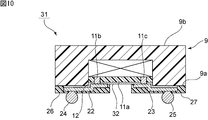
- FIG. 10 is a front cross-sectional view of an electronic component obtained in the third embodiment of the present invention.
- a resin layer 32 is provided on the base of the wirings 22 and 23.
- the resin layer 32 is not only laminated on the wirings 22 and 23 as a base of the wirings 22 and 23 but also reaches the resin layer 11 a of the electronic component element 11.
- the resin layer 32 is preferably made of a resin having excellent heat resistance such as polyimide or epoxy resin. But the resin material which comprises the resin layer 32 is not necessarily limited. When the resin layer 32 is provided, the adhesion between the wirings 22 and 23 and the resin layer 11a of the electronic component element 11 is enhanced.
- the other components of the electronic component 31 are the same as those of the electronic component 28. Therefore, the same parts are denoted by the same reference numerals, and the description thereof is omitted.
- a resin layer similar to the resin layer 32 may be provided so as to serve as a base for the wirings 14 and 15 and to be in contact with the resin layer 11a. Good.
- the newly provided resin layer is provided so as not to cover the terminals 11b and 11c as in the case of FIG.
Landscapes
- Production Of Multi-Layered Print Wiring Board (AREA)
- Encapsulation Of And Coatings For Semiconductor Or Solid State Devices (AREA)
Abstract
樹脂構造体に内蔵された電子部品素子の位置ずれが生じ難い電子部品の製造方法を提供する。 金属シート3上に粘着剤層8を形成する工程と、粘着剤層8上に電子部品素子11を積層し、仮固定する工程と、仮固定されている電子部品素子11を埋め込むように、金型内において、樹脂材料を投入し、プレスすることにより、樹脂材料を金属シート3上に付与する工程と、樹脂材料を硬化させて、樹脂構造体9を形成する工程と、金属シート3及び粘着剤層8を除去して電子部品を製造する工程と、を備える、電子部品の製造方法。
Description
本発明は、樹脂構造体に電子部品素子が内蔵されている電子部品及びその製造方法に関する。
従来、樹脂構造体に電子部品素子が内蔵されている、部品内蔵型の電子部品が知られている。下記の特許文献1に記載の製造方法では、ベース材上に半導体チップを搭載する。しかる後、半導体チップを埋め込むように樹脂材料を付与する。この樹脂材料を硬化させ、樹脂構造体を形成する。そして、ベース材を隔離する。それによって、樹脂構造体に半導体チップが内蔵されている電子部品が得られる。この電子部品では、半導体チップのベース材と接触していた部分が、表面に露出される。
特許文献1に記載のような部品内蔵型の電子部品を得るにあたっては、部品内蔵型の電子部品の構成要素である樹脂構造体の形成に際し、電子部品素子と熱硬化性樹脂を金型内において充填し、プレスする。そして、加熱により熱硬化性樹脂を硬化させ、樹脂構造体を得る。ところが、このプレス時の圧力や加熱硬化に際しての硬化収縮により、電子部品素子の位置ずれが生じることがあった。
本発明の目的は、樹脂構造体に内蔵された電子部品素子の位置ずれが生じ難い電子部品の製造方法、及び電子部品素子の位置精度が高められた電子部品を提供することにある。
本発明に係る電子部品の製造方法は、金属シート上に粘着剤層を形成する工程と、前記粘着剤層上に、電子部品素子を積層し、仮固定する工程と、前記仮固定されている前記電子部品素子を埋め込むように、金型内において樹脂材料を投入し、プレスすることにより、前記樹脂材料を前記金属シート上に付与する工程と、前記樹脂材料を硬化させて、樹脂構造体を形成する工程と、前記金属シート及び前記粘着剤層を除去して電子部品を製造する工程と、を備える。
本発明に係る電子部品の製造方法のある特定の局面では、前記樹脂材料を付与する前に、前記電子部品素子の下方の領域以外の少なくとも一部の領域において前記粘着剤層を除去する工程がさらに備えられている。この場合には、粘着剤層が除去されている領域において、樹脂材料が金属シートに接触する。従って、樹脂硬化時の電子部品素子の位置ずれをより一層効果的に抑制することができる。
本発明に係る電子部品の製造方法の他の特定の局面では、前記粘着剤層の少なくとも一部を除去するにあたり、前記電子部品素子の下方の領域以外の全領域において、前記粘着剤層を除去する。この場合には、電子部品素子の位置ずれをさらに効果的に抑制することができる。
本発明に係る電子部品の製造方法の別の特定の局面では、前記粘着剤層の形成に先立ち、前記金属シート上に、柱状の電極を設ける工程をさらに備え、前記柱状の電極が、前記樹脂材料を封止した後に、前記樹脂構造体を貫通している貫通電極となる。
本発明に係る電子部品の製造方法のさらに他の特定の局面では、前記金属シート及び前記粘着剤層を除去した後に、前記樹脂構造体に、前記電子部品素子に接続されており、前記樹脂構造体の外表面に至っている配線を設ける工程がさらに備えられている。
本発明に係る電子部品の製造方法のさらに他の特定の局面では、前記金属シートの前記粘着剤層が設けられる側とは反対側の面に積層されている支持板が設けられており、前記支持板に支持された前記金属シート上に前記粘着剤層が形成される。この場合には、支持板によって金属シートが補強されているため、電子部品素子の位置ずれをより効果的に抑制することができる。
本発明に係る電子部品の製造方法のさらに他の特定の局面では、前記支持板は、樹脂、金属及びシリコンからなる群から選択された1種の材料からなる。
本発明に係る電子部品は、対向し合う第1の面と第2の面とを有する樹脂構造体と、前記樹脂構造体に内蔵されており、前記樹脂構造体における前記第1の面に露出している電子部品素子と、前記樹脂構造体における前記第1の面に設けられており、前記電子部品素子に接続されている配線と、を備え、前記電子部品素子における前記第1の面側の面と、前記樹脂構造体における前記第1の面との間に段差があり、前記電子部品素子における前記第1の面側の面が、前記第1の面よりも前記樹脂構造体の内側にある。
本発明に係る電子部品のある特定の局面では、前記樹脂構造体における前記第1の面と前記第2の面とを貫通している貫通電極がさらに備えられている。
本発明に係る部品内蔵型の電子部品の製造方法によれば、電子部品の構成要素である樹脂構造体を形成するに際し、樹脂構造体に内蔵された電子部品素子の位置ずれが生じ難い。また、樹脂構造体に内蔵された電子部品素子の位置精度が高められた、部品内蔵型の電子部品を提供することができる。
以下、図面を参照しつつ、本発明の具体的な実施形態を説明することにより、本発明を明らかにする。
なお、本明細書に記載の各実施形態は、例示的なものであり、異なる実施形態間において、構成の部分的な置換または組み合わせが可能であることを指摘しておく。
(第1の実施形態の電子部品の製造方法)
図1(a)及び図1(b)~図5を参照して、第1の実施形態の電子部品の製造方法を説明する。
図1(a)及び図1(b)~図5を参照して、第1の実施形態の電子部品の製造方法を説明する。
まず、図1(a)に示す積層体4を用意する。積層体4では、樹脂、金属、セラミックス及びシリコンからなる群から選択された1種の材料からなる支持板1上に、接着材2を介して、金属シート3が積層されている。金属シート3は、本実施形態では金属箔からなるが、金属板であってもよい。金属シート3の金属としては、特に限定されず、Cu、Alなどを用いることができる。
なお、接着材2は、ガラスエポキシ樹脂のような接着剤であってもよく、両面接着型の粘着テープであってもよい。
次に、図1(b)に示すレジストパターン5を形成する。レジストパターン5は、貫通孔5a,5bを有する。レジストパターン5を形成した後に、電界めっき法により、貫通電極6,7を形成する。すなわち、電界めっき法により、金属シート3上にめっき膜を成長させる。それによって、柱状の電極を形成する。
この柱状の電極は、後述するように、最終的に樹脂構造体を貫いている貫通電極6,7に相当する。
従って、図1(b)の段階においても柱状の電極を貫通電極6,7と表現する。貫通電極6,7の材料としては、Cuなどの適宜の金属もしくは合金を用いることができる。
次に、レジストパターン5を剥離する。このようにして、図2(a)に示すように、貫通電極6,7が、上方に突出した状態で得られる。次に、電子部品素子が配置される領域に、図2(b)に示すように粘着剤層8を設ける。この粘着剤層8を設けるに際しては、金属シート3上の全面に粘着剤層を形成した後、パターニングする。別の方法として、電子部品素子が配置される領域を開口部とするマスクを配置した後に、粘着剤を塗布してもよい。粘着剤層8の材料としては、特に限定されないが、本実施形態では、光の照射により露光し、現像することにより除去し得る粘着性フォトレジストが用いられる。
次に図3(a)に示すように、上記粘着剤層8上に、電子部品素子11を貼り付ける。電子部品素子11は、その詳細は省略するが、本実施形態では、粘着剤層8と接触する側の面に樹脂層11aを有する。樹脂層11aを貫通するように、端子11b,11cが設けられている。端子11b,11cは、電子部品素子11内の機能電極などに電気的に接続されている。
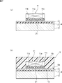
次に、金型内に、図3(a)に示した構造を配置し、電子部品素子11が埋め込まれるように、樹脂材料を付与する。樹脂材料としては、エポキシ樹脂などの適宜の熱硬化性樹脂が用いられる。そして、プレスしつつ、加熱により樹脂材料を硬化させる。このようにして、図3(b)に示す樹脂構造体9を形成する。樹脂構造体9は、対向し合う第1の面9aと第2の面9bとを有する。電子部品素子11は、樹脂構造体9により封止されている。そして、この場合、樹脂構造体9の第1の面9aが、金属シート3の上面に密着している。
上記のように、樹脂構造体9の形成に際しては、プレスによる応力が樹脂材料を通じて電子部品素子11に伝わる。また、加熱硬化時の硬化収縮による応力も電子部品素子11に加わる。しかしながら、電子部品素子11が、粘着剤層8により金属シート3に接合されている。また金属シート3の剛性は比較的高く、しかも支持板1によって支持されている。よって、上記のような応力が加わったとしても、電子部品素子11の位置ずれが生じ難い。
次に、エッチングにより、金属シート3を溶解し、積層体4を除去する。また、光の照射による露光及び現像により、フォトレジストからなる粘着剤層8を除去する。このようにして、図4(a)に示す構造が得られる。
図4(a)では、電子部品素子11の下面すなわち樹脂層11aの外側の面と、樹脂構造体9の第1の面9aとの間に段差12が設けられている。すなわち、樹脂層11aの外側の面は、第1の面9aよりも、樹脂構造体9の内側の位置にある。そのため、凹部13が設けられている。
次に、図4(b)に示すように、樹脂構造体9の第1の面9a上に、配線14,15を設ける。配線14は、樹脂構造体9の第1の面9a上において、貫通電極6に接続されている。また、配線14は、樹脂層11aの外側の面、すなわち外表面に至っており、端子11bに電気的に接続されている。配線15も、樹脂構造体9の第1の面9aから、樹脂層11aの外側面に至っている。そして、配線15は、貫通電極7と、端子11cとを電気的に接続している。
なお、配線14,15は、一層だけでなく、複数層が積層されていてもよい。複数層が積層されている場合には、各層の間に絶縁層が形成されている。
図4(b)に示す電子部品16では、樹脂構造体9内における電子部品素子11の位置精度は充分に高い。
次に、必要に応じて、図5に示すように、他の電子部品18を積層する。電子部品18は、金属バンプ19a,19bを有する。この金属バンプ19a,19bが、配線14,15に接続される。また、上記電子部品16の下面側にも、さらに他の電子部品を配置し、貫通電極6,7と電気的に接続してもよい。すなわち、電子部品16は、複数の電子部品間を電気的に接続するインターポーザとして好適に用いることができる。
なお、上記電子部品素子11は特に限定されず、弾性波素子やコンデンサなどの受動部品や、半導体素子のような能動部品のいずれであってもよい。他の電子部品18についても特に限定されない。
また、図5に破線Xで示すように、貫通電極6,7の下端側に、さらに別の電子部品が積層されていてもよい。すなわち、破線Xで示す電子部品と、電子部品18とを電気的に接続するインターポーザとして電子部品16を用いてもよい。
(第2の実施形態の電子部品の製造方法)
図6(a)及び図6(b)~図9を参照して、第2の実施形態の電子部品の製造方法を説明する。
図6(a)及び図6(b)~図9を参照して、第2の実施形態の電子部品の製造方法を説明する。
まず、図6(a)に示すように、第1の実施形態の場合と同様に、支持板1、接着材2及び金属シート3を有する積層体4を用意する。次に、図6(b)に示すように、金属シート3上の全面に粘着剤層21を設ける。この粘着剤層21については、粘着剤層8と同様に粘着性フォトレジストが用いられ得る。もっとも、粘着剤層21は、後工程においてパターニングし、かつ除去し得る適宜の材料により形成することができる。
次に、粘着剤層21上に、電子部品素子11を貼り合せる。電子部品素子11をマスクとして、上方から光を照射し、露光・現像により、粘着剤層21の一部を除去する。この場合、電子部品素子11がマスクとして用いられているため、電子部品素子11の下方の領域を除く残りの領域の粘着剤層21が除去される。従って、図7(a)に示すように、電子部品素子11の下方にのみ粘着剤層21が残る。この状態において、電子部品素子11は、粘着剤層21により、金属シート3に接合されている。第1の実施形態の場合と同様に、金型内に得られた構造を配置し、熱硬化性樹脂からなる樹脂材料を用いて、電子部品素子11を封止するとともに、電子部品素子11を埋設させる。そして、プレスしつつ加熱することにより、樹脂材料を硬化させる。このようにして、図7(b)に示す樹脂構造体9を形成する。
樹脂構造体9の第1の面9aと、粘着剤層21の下面すなわち外側の面とが面一とされている。樹脂層11aの下面すなわち外側の面は、第1の面9aよりも、樹脂構造体9の内側に後退している。すなわち、第1の実施形態の場合と同様に、樹脂層11aの外側の面と、第1の面9aとの間に、段差12が設けられている。本実施形態においても、上記粘着剤層21に、電子部品素子11が金属シート3に接合されている状態で樹脂構造体9が形成される。従って、プレス時の圧力や熱硬化時の硬化収縮による応力が電子部品素子11に加わったとしても、電子部品素子11の位置ずれが生じ難い。
次に、接着材2と金属シート3との界面で剥離する。なお、支持板が樹脂の場合には、支持板が弾性を持つため、接着材2と金属シート3との界面での剥離の際に、支持板を弾性変形させることで剥離が容易となる。
このようにして、図8(a)に示す構造が得られる。しかる後、金属シート3をエッチングにより除去し、粘着剤層21を溶剤により溶解し除去する。このようにして、図8(b)に示す構造が得られる。
さらに、図9に示すように、配線22,23を設ける。配線22,23は、樹脂構造体9の第1の面9aから、段差12を介して樹脂層11aの外側の面に至っている。配線22は、端子11bに接続されている。配線23は、端子11cに接続されている。
また、配線22,23の周囲に、絶縁性材料からなる絶縁層26,27を形成する。絶縁性材料としては、合成樹脂や無機絶縁材料を用いることができる。そして、第1の面9a上において、配線22,23の外側面に金属バンプ24,25を設ける。
第2の実施形態では、図9に示すように、金属バンプ24,25を有する電子部品28を得ることができる。この電子部品28においても、樹脂構造体9内において、電子部品素子11の位置精度が高められている。電子部品28は、金属バンプ24,25を用いて、実装基板などに実装され得る。
なお、第1,第2の実施形態において、樹脂層11aを有しない電子部品素子11を樹脂構造体9内に埋設してもよい。例えば、弾性表面波素子などの一方面が振動する部品の場合、上記樹脂層11aを設けずに、樹脂層11aが設けられている部分を空間としてもよい。あるいは、WLP型の弾性波装置のように、カバー層としての樹脂層11aを有する弾性波装置を電子部品素子11として用いてもよい。
図10は、本発明の第3の実施形態で得られる電子部品の正面断面図である。電子部品31では、配線22,23の下地に、樹脂層32が設けられている。この樹脂層32は、配線22,23の下地として、配線22,23に積層されているだけでなく、電子部品素子11の樹脂層11a上にも至っている。樹脂層32は、ポリイミドやエポキシ樹脂などの耐熱性に優れた樹脂からなることが望ましい。もっとも、樹脂層32を構成する樹脂材料は特に限定されるわけではない。樹脂層32が設けられていると、配線22,23と電子部品素子11の樹脂層11aとの密着性が高められる。
電子部品31は、その他の構造は、電子部品28と同様である。従って、同一部分については同一の参照番号を付することにより、その説明を省略する。
また、図5に示した電子部品16においても、同様に、配線14,15の下地となるように、また樹脂層11aと接触するように、上記樹脂層32と同様の樹脂層を設けてもよい。この場合、新たに設けられた樹脂層は、図10の場合と同様に、端子11b,11cを覆わないように設けられる。
1…支持板
2…接着材
3…金属シート
4…積層体
5…レジストパターン
5a,5b…貫通孔
6,7…貫通電極
8…粘着剤層
9…樹脂構造体
9a…第1の面
9b…第2の面
11…電子部品素子
11a…樹脂層
11b,11c…端子
12…段差
13…凹部
14,15…配線
16,18…電子部品
19a,19b…金属バンプ
21…粘着剤層
22,23…配線
24,25…金属バンプ
26,27…絶縁層
28…電子部品
31…電子部品
32…樹脂層
2…接着材
3…金属シート
4…積層体
5…レジストパターン
5a,5b…貫通孔
6,7…貫通電極
8…粘着剤層
9…樹脂構造体
9a…第1の面
9b…第2の面
11…電子部品素子
11a…樹脂層
11b,11c…端子
12…段差
13…凹部
14,15…配線
16,18…電子部品
19a,19b…金属バンプ
21…粘着剤層
22,23…配線
24,25…金属バンプ
26,27…絶縁層
28…電子部品
31…電子部品
32…樹脂層
Claims (9)
- 金属シート上に粘着剤層を形成する工程と、
前記粘着剤層上に電子部品素子を積層し、仮固定する工程と、
前記仮固定されている前記電子部品素子を埋め込むように、金型内において樹脂材料を投入し、プレスすることにより、前記樹脂材料を前記金属シート上に付与する工程と、
前記樹脂材料を硬化させて、樹脂構造体を形成する工程と、
前記金属シート及び前記粘着剤層を除去して電子部品を製造する工程と、
を備える、電子部品の製造方法。 - 前記樹脂材料を付与する前に、前記電子部品素子の下方の領域以外の少なくとも一部の領域において前記粘着剤層を除去する工程をさらに備える、請求項1に電子部品の製造方法。
- 前記粘着剤層の少なくとも一部を除去するにあたり、前記電子部品素子の下方の領域以外の全領域において、前記粘着剤層を除去する、請求項2に記載の電子部品の製造方法。
- 前記粘着剤層の形成に先立ち、前記金属シート上に、柱状の電極を設ける工程をさらに備え、前記柱状の電極が、前記樹脂材料を封止した後に、前記樹脂構造体を貫通している貫通電極となる、請求項1~3のいずれか1項に記載の電子部品の製造方法。
- 前記金属シート及び前記粘着剤層を除去した後に、前記樹脂構造体に、前記電子部品素子に接続されており、前記樹脂構造体の外表面に至っている配線を設ける工程をさらに備える、請求項1~4のいずれか1項に記載の電子部品の製造方法。
- 前記金属シートの前記粘着剤層が設けられる側とは反対側の面に積層されている支持板が設けられており、前記支持板に支持された前記金属シート上に前記粘着剤層が形成される、請求項1~5のいずれか1項に記載の電子部品の製造方法。
- 前記支持板は、樹脂、金属及びシリコンからなる群から選択された1種の材料からなる、請求項6に記載の電子部品の製造方法。
- 対向し合う第1の面と第2の面とを有する樹脂構造体と、
前記樹脂構造体に内蔵されており、前記樹脂構造体における前記第1の面に露出している電子部品素子と、
前記樹脂構造体における前記第1の面に設けられており、前記電子部品素子に接続されている配線と、
を備え、
前記電子部品素子における前記第1の面側の面と、前記樹脂構造体における前記第1の面との間に段差があり、
前記電子部品素子における前記第1の面側の面が、前記第1の面よりも前記樹脂構造体の内側にある、電子部品。 - 前記樹脂構造体における前記第1の面と前記第2の面とを貫通している貫通電極をさらに備える、請求項8に記載の電子部品。
Priority Applications (1)
| Application Number | Priority Date | Filing Date | Title |
|---|---|---|---|
| CN201780065992.8A CN109906506A (zh) | 2016-11-28 | 2017-10-12 | 电子部件及其制造方法 |
Applications Claiming Priority (2)
| Application Number | Priority Date | Filing Date | Title |
|---|---|---|---|
| JP2016229849 | 2016-11-28 | ||
| JP2016-229849 | 2016-11-28 |
Publications (1)
| Publication Number | Publication Date |
|---|---|
| WO2018096830A1 true WO2018096830A1 (ja) | 2018-05-31 |
Family
ID=62195549
Family Applications (1)
| Application Number | Title | Priority Date | Filing Date |
|---|---|---|---|
| PCT/JP2017/037019 Ceased WO2018096830A1 (ja) | 2016-11-28 | 2017-10-12 | 電子部品及びその製造方法 |
Country Status (2)
| Country | Link |
|---|---|
| CN (1) | CN109906506A (ja) |
| WO (1) | WO2018096830A1 (ja) |
Cited By (1)
| Publication number | Priority date | Publication date | Assignee | Title |
|---|---|---|---|---|
| WO2020066490A1 (ja) * | 2018-09-28 | 2020-04-02 | 株式会社村田製作所 | 積層体および積層体の製造方法 |
Citations (6)
| Publication number | Priority date | Publication date | Assignee | Title |
|---|---|---|---|---|
| JP2009054666A (ja) * | 2007-08-24 | 2009-03-12 | Casio Comput Co Ltd | 半導体装置およびその製造方法 |
| JP2009530801A (ja) * | 2006-03-17 | 2009-08-27 | インベラ エレクトロニクス オサケユキチュア | 回路基板の製造方法とコンポーネントを有する回路基板 |
| JP2010199129A (ja) * | 2009-02-23 | 2010-09-09 | Shinko Electric Ind Co Ltd | 半導体装置及びその製造方法、並びに電子装置 |
| US20110147911A1 (en) * | 2009-12-22 | 2011-06-23 | Epic Technologies, Inc. | Stackable circuit structures and methods of fabrication thereof |
| JP2013258238A (ja) * | 2012-06-12 | 2013-12-26 | Fujitsu Ltd | 電子装置及びその製造方法 |
| JP2016178108A (ja) * | 2015-03-18 | 2016-10-06 | 日立化成株式会社 | 半導体装置の製造方法 |
Family Cites Families (2)
| Publication number | Priority date | Publication date | Assignee | Title |
|---|---|---|---|---|
| JP2007305714A (ja) * | 2006-05-10 | 2007-11-22 | Sharp Corp | 半導体装置及びその製造方法 |
| JP5496692B2 (ja) * | 2010-01-22 | 2014-05-21 | 三洋電機株式会社 | 半導体モジュールの製造方法 |
-
2017
- 2017-10-12 WO PCT/JP2017/037019 patent/WO2018096830A1/ja not_active Ceased
- 2017-10-12 CN CN201780065992.8A patent/CN109906506A/zh active Pending
Patent Citations (6)
| Publication number | Priority date | Publication date | Assignee | Title |
|---|---|---|---|---|
| JP2009530801A (ja) * | 2006-03-17 | 2009-08-27 | インベラ エレクトロニクス オサケユキチュア | 回路基板の製造方法とコンポーネントを有する回路基板 |
| JP2009054666A (ja) * | 2007-08-24 | 2009-03-12 | Casio Comput Co Ltd | 半導体装置およびその製造方法 |
| JP2010199129A (ja) * | 2009-02-23 | 2010-09-09 | Shinko Electric Ind Co Ltd | 半導体装置及びその製造方法、並びに電子装置 |
| US20110147911A1 (en) * | 2009-12-22 | 2011-06-23 | Epic Technologies, Inc. | Stackable circuit structures and methods of fabrication thereof |
| JP2013258238A (ja) * | 2012-06-12 | 2013-12-26 | Fujitsu Ltd | 電子装置及びその製造方法 |
| JP2016178108A (ja) * | 2015-03-18 | 2016-10-06 | 日立化成株式会社 | 半導体装置の製造方法 |
Cited By (3)
| Publication number | Priority date | Publication date | Assignee | Title |
|---|---|---|---|---|
| WO2020066490A1 (ja) * | 2018-09-28 | 2020-04-02 | 株式会社村田製作所 | 積層体および積層体の製造方法 |
| CN112740382A (zh) * | 2018-09-28 | 2021-04-30 | 株式会社村田制作所 | 层叠体及层叠体的制造方法 |
| US12002779B2 (en) | 2018-09-28 | 2024-06-04 | Murata Manufacturing Co., Ltd. | Multilayer body and method of manufacturing the same |
Also Published As
| Publication number | Publication date |
|---|---|
| CN109906506A (zh) | 2019-06-18 |
Similar Documents
| Publication | Publication Date | Title |
|---|---|---|
| JP5395360B2 (ja) | 電子部品内蔵基板の製造方法 | |
| JP4361826B2 (ja) | 半導体装置 | |
| JP5175719B2 (ja) | 回路基板構造の製造方法及び回路基板構造 | |
| JP6342120B2 (ja) | 超薄埋設ダイモジュール及びその製造方法 | |
| CN101010994B (zh) | 制造电子模块的方法 | |
| CN103650650B (zh) | 印刷电路板及其制造方法 | |
| JP5289832B2 (ja) | 半導体装置および半導体装置の製造方法 | |
| CN104756615B (zh) | 印刷电路板 | |
| WO2015083345A1 (ja) | 部品内蔵配線基板及びその製造方法 | |
| KR20090033004A (ko) | 배선 기판 및 그 제조 방법 | |
| KR101701380B1 (ko) | 소자 내장형 연성회로기판 및 이의 제조방법 | |
| KR101522780B1 (ko) | 전자부품 내장 인쇄회로기판 및 그 제조방법 | |
| KR20080031107A (ko) | 반도체 장치 | |
| CN102881605B (zh) | 用于制造半导体封装的方法 | |
| JP5200870B2 (ja) | 部品内蔵モジュールの製造方法 | |
| WO2018096830A1 (ja) | 電子部品及びその製造方法 | |
| JP6266908B2 (ja) | 電子部品内蔵基板の製造方法 | |
| US11004759B2 (en) | Electronic component and method for manufacturing the same | |
| JP2015109346A (ja) | 部品内蔵配線基板及びその製造方法 | |
| JP2014116640A (ja) | 半導体装置及びその製造方法 | |
| JP5772134B2 (ja) | 回路基板、その製造方法および半導体装置 | |
| JP5671857B2 (ja) | 埋め込み部品具有配線板の製造方法 | |
| JP2017069446A (ja) | プリント配線板およびその製造方法 | |
| KR20150136653A (ko) | 회로기판 및 제조방법 | |
| JP2009043858A (ja) | 半導体装置およびその製造方法 |
Legal Events
| Date | Code | Title | Description |
|---|---|---|---|
| 121 | Ep: the epo has been informed by wipo that ep was designated in this application |
Ref document number: 17874679 Country of ref document: EP Kind code of ref document: A1 |
|
| NENP | Non-entry into the national phase |
Ref country code: DE |
|
| 122 | Ep: pct application non-entry in european phase |
Ref document number: 17874679 Country of ref document: EP Kind code of ref document: A1 |
|
| NENP | Non-entry into the national phase |
Ref country code: JP |