WO2018084129A1 - 表面導電性積層シート及び電子部品包装容器 - Google Patents
表面導電性積層シート及び電子部品包装容器 Download PDFInfo
- Publication number
- WO2018084129A1 WO2018084129A1 PCT/JP2017/039258 JP2017039258W WO2018084129A1 WO 2018084129 A1 WO2018084129 A1 WO 2018084129A1 JP 2017039258 W JP2017039258 W JP 2017039258W WO 2018084129 A1 WO2018084129 A1 WO 2018084129A1
- Authority
- WO
- WIPO (PCT)
- Prior art keywords
- resin
- laminated sheet
- electronic component
- conjugated diene
- mass
- Prior art date
- Legal status (The legal status is an assumption and is not a legal conclusion. Google has not performed a legal analysis and makes no representation as to the accuracy of the status listed.)
- Ceased
Links
Classifications
-
- B—PERFORMING OPERATIONS; TRANSPORTING
- B32—LAYERED PRODUCTS
- B32B—LAYERED PRODUCTS, i.e. PRODUCTS BUILT-UP OF STRATA OF FLAT OR NON-FLAT, e.g. CELLULAR OR HONEYCOMB, FORM
- B32B7/00—Layered products characterised by the relation between layers; Layered products characterised by the relative orientation of features between layers, or by the relative values of a measurable parameter between layers, i.e. products comprising layers having different physical, chemical or physicochemical properties; Layered products characterised by the interconnection of layers
- B32B7/02—Physical, chemical or physicochemical properties
- B32B7/025—Electric or magnetic properties
-
- B—PERFORMING OPERATIONS; TRANSPORTING
- B32—LAYERED PRODUCTS
- B32B—LAYERED PRODUCTS, i.e. PRODUCTS BUILT-UP OF STRATA OF FLAT OR NON-FLAT, e.g. CELLULAR OR HONEYCOMB, FORM
- B32B27/00—Layered products comprising a layer of synthetic resin
- B32B27/06—Layered products comprising a layer of synthetic resin as the main or only constituent of a layer, which is next to another layer of the same or of a different material
- B32B27/08—Layered products comprising a layer of synthetic resin as the main or only constituent of a layer, which is next to another layer of the same or of a different material of synthetic resin
-
- B—PERFORMING OPERATIONS; TRANSPORTING
- B32—LAYERED PRODUCTS
- B32B—LAYERED PRODUCTS, i.e. PRODUCTS BUILT-UP OF STRATA OF FLAT OR NON-FLAT, e.g. CELLULAR OR HONEYCOMB, FORM
- B32B27/00—Layered products comprising a layer of synthetic resin
- B32B27/18—Layered products comprising a layer of synthetic resin characterised by the use of special additives
-
- B—PERFORMING OPERATIONS; TRANSPORTING
- B32—LAYERED PRODUCTS
- B32B—LAYERED PRODUCTS, i.e. PRODUCTS BUILT-UP OF STRATA OF FLAT OR NON-FLAT, e.g. CELLULAR OR HONEYCOMB, FORM
- B32B27/00—Layered products comprising a layer of synthetic resin
- B32B27/18—Layered products comprising a layer of synthetic resin characterised by the use of special additives
- B32B27/20—Layered products comprising a layer of synthetic resin characterised by the use of special additives using fillers, pigments, thixotroping agents
-
- B—PERFORMING OPERATIONS; TRANSPORTING
- B32—LAYERED PRODUCTS
- B32B—LAYERED PRODUCTS, i.e. PRODUCTS BUILT-UP OF STRATA OF FLAT OR NON-FLAT, e.g. CELLULAR OR HONEYCOMB, FORM
- B32B27/00—Layered products comprising a layer of synthetic resin
- B32B27/30—Layered products comprising a layer of synthetic resin comprising vinyl (co)polymers; comprising acrylic (co)polymers
-
- B—PERFORMING OPERATIONS; TRANSPORTING
- B32—LAYERED PRODUCTS
- B32B—LAYERED PRODUCTS, i.e. PRODUCTS BUILT-UP OF STRATA OF FLAT OR NON-FLAT, e.g. CELLULAR OR HONEYCOMB, FORM
- B32B27/00—Layered products comprising a layer of synthetic resin
- B32B27/30—Layered products comprising a layer of synthetic resin comprising vinyl (co)polymers; comprising acrylic (co)polymers
- B32B27/302—Layered products comprising a layer of synthetic resin comprising vinyl (co)polymers; comprising acrylic (co)polymers comprising aromatic vinyl (co)polymers, e.g. styrenic (co)polymers
-
- B—PERFORMING OPERATIONS; TRANSPORTING
- B65—CONVEYING; PACKING; STORING; HANDLING THIN OR FILAMENTARY MATERIAL
- B65D—CONTAINERS FOR STORAGE OR TRANSPORT OF ARTICLES OR MATERIALS, e.g. BAGS, BARRELS, BOTTLES, BOXES, CANS, CARTONS, CRATES, DRUMS, JARS, TANKS, HOPPERS, FORWARDING CONTAINERS; ACCESSORIES, CLOSURES, OR FITTINGS THEREFOR; PACKAGING ELEMENTS; PACKAGES
- B65D65/00—Wrappers or flexible covers; Packaging materials of special type or form
- B65D65/38—Packaging materials of special type or form
- B65D65/40—Applications of laminates for particular packaging purposes
-
- B—PERFORMING OPERATIONS; TRANSPORTING
- B32—LAYERED PRODUCTS
- B32B—LAYERED PRODUCTS, i.e. PRODUCTS BUILT-UP OF STRATA OF FLAT OR NON-FLAT, e.g. CELLULAR OR HONEYCOMB, FORM
- B32B2264/00—Composition or properties of particles which form a particulate layer or are present as additives
- B32B2264/10—Inorganic particles
- B32B2264/107—Ceramic
- B32B2264/108—Carbon, e.g. graphite particles
-
- B—PERFORMING OPERATIONS; TRANSPORTING
- B32—LAYERED PRODUCTS
- B32B—LAYERED PRODUCTS, i.e. PRODUCTS BUILT-UP OF STRATA OF FLAT OR NON-FLAT, e.g. CELLULAR OR HONEYCOMB, FORM
- B32B2307/00—Properties of the layers or laminate
- B32B2307/20—Properties of the layers or laminate having particular electrical or magnetic properties, e.g. piezoelectric
- B32B2307/202—Conductive
-
- B—PERFORMING OPERATIONS; TRANSPORTING
- B32—LAYERED PRODUCTS
- B32B—LAYERED PRODUCTS, i.e. PRODUCTS BUILT-UP OF STRATA OF FLAT OR NON-FLAT, e.g. CELLULAR OR HONEYCOMB, FORM
- B32B2553/00—Packaging equipment or accessories not otherwise provided for
Definitions
- the present invention relates to a surface conductive laminated sheet made of a thermoplastic resin, and an electronic component packaging container such as a carrier tape and an electronic component carrying tray using the laminated sheet.
- ⁇ Vacuum forming trays, embossed carrier tapes, etc. obtained by heat forming sheets are used for packaging containers for intermediate products of all industrial products such as electronic devices and automobiles. And as a sheet for packaging containers of various electronic parts having ICs that dislike static electricity, a sheet in which a polystyrene resin in which a conductive filler such as carbon black is contained is laminated on a base material layer made of polystyrene resin. (See, for example, Patent Documents 1 to 3).
- the pickup nozzle does not contact the carrier tape and is accurate It has become very difficult to pick up electronic components.
- the pickup nozzle comes into contact with the carrier tape, the carrier tape is crushed or deformed, which causes a so-called pickup failure that occurs when the pickup path is obstructed.
- the present invention for example, in a conductive carrier tape, a surface conductive laminate sheet that can suppress the crushing and deformation of the carrier tape even when the pickup nozzle contacts the carrier tape during electronic component mounting, and has excellent strength, and It is an object of the present invention to provide an electronic component packaging container formed by molding it, more specifically, a carrier tape or an electronic component transport tray.
- the present inventors have found that the surface conductive laminate has solved all of the above problems by including a polystyrene resin having a conjugated diene content in a specific range in the base material layer and the surface layer.
- the inventors have found that a sheet can be obtained and have reached the present invention.
- the conjugated diene content is 2.0 to 7.4% by mass on both sides of a sheet base material layer made of polystyrene resin having a conjugated diene content of 3.0 to 8.2% by mass.
- a surface conductive laminated sheet having a Martens hardness of 50 to 130 N / mm 2 in which a surface layer made of a conductive resin composition containing a polystyrene resin and a conductive filler is laminated.
- the conductive filler is preferably carbon black.
- the conductive resin composition of the surface layer preferably further contains a hydrogenated resin of an olefin resin and an aromatic vinyl-conjugated diene block copolymer.
- the surface layer is hydrogenated of 46 to 85% by weight of polystyrene resin, 13 to 23% by weight of carbon black, 1.5 to 20% by weight of olefin resin, and aromatic vinyl-conjugated diene block copolymer.
- the resin preferably contains 0.5 to 11% by mass.
- the volume average particle diameter of the conjugated diene contained in the polystyrene resin used for the base material layer and the surface layer is preferably 0.5 to 4.0 ⁇ m.
- the present invention includes an electronic component packaging container formed from the surface conductive laminated sheet, specifically, a carrier tape or an electronic component transport tray.
- the pickup nozzle is used as the carrier tape when electronic components are mounted. Even if it contacts, the crushing and deformation
- the surface conductive laminate sheet according to one embodiment of the present invention is composed of a base material layer mainly composed of polystyrene (PS) resin and a conductive surface layer laminated on both surfaces of the base material layer.
- PS polystyrene
- Polystyrene (PS) resin means a resin mainly composed of polystyrene resin (GPPS), impact-resistant polystyrene resin (rubber-modified styrene resin, HIPS) or a mixture thereof.
- the aromatic vinyl monomer constituting the polystyrene resin include styrene, o-methyl styrene, p-methyl styrene, p-tert-butyl styrene, 1,3-dimethyl styrene, ⁇ -methyl styrene, vinyl naphthalene. Vinyl anthracene, 1,1-diphenylethylene and the like.
- the impact-resistant polystyrene resin is a polystyrene resin in which a styrene monomer is graft-polymerized on a rubber-like elastic body mainly composed of a conjugated diene.
- the conjugated dienes used are 1,3-butadiene, 2-methyl-1,3-butadiene (isoprene), 2,3-dimethyl-1,3-butadiene, 1,3-pentadiene, 1,3-hexadiene
- a particularly common one is 1,3-butadiene.
- the polystyrene resin used for the base layer contains 3.0 to 8.2% by mass, preferably 3.0 to 5.0% by mass of the conjugated diene, and 2 conjugated dienes are contained in the polystyrene resin used for the surface layer. It is contained in an amount of 0.0 to 7.4% by mass, preferably 2.0 to 4.0% by mass.
- the content of the conjugated diene in the polystyrene-based resin is a simple method to adjust by blending GPPS and HIPS, but it may be adjusted at the manufacturing stage of HIPS.
- the melt flow index (measured according to JIS-K-7210) of GPPS and HIPS used for the base material layer and the surface layer is not particularly limited, but is 1 to 15 g under the conditions of 200 ° C. and a load of 5 kg. A product of / 10 minutes is suitably used on the molding surface.
- the content of the polystyrene resin in the surface layer is preferably 46 to 85% by mass, more preferably 54 to 81% by mass, and still more preferably 58 to 80% by mass.
- the electroconductive fall accompanying the fall of the addition amount ratio of an electroconductive filler is suppressed, and it is suppressed that a tensile elasticity modulus becomes small by setting it as 46 mass% or more.
- the volume average particle diameter of the conjugated diene contained in the polystyrene resin used for the base material layer and the surface layer is preferably 0.5 to 4.0 ⁇ m, more preferably 2.0 to 3.5 ⁇ m. More preferably, the thickness is 2.4 to 3.0 ⁇ m. Good mechanical performance can be obtained when the volume average particle diameter is in the above range. When the volume average particle size is 4.0 ⁇ m or less, the decrease in tensile elastic modulus is suppressed, and when the volume average particle size is 0.5 ⁇ m or more, the bending strength is suppressed from decreasing.
- the conductive filler contained in the surface layer is not particularly limited, but carbon black is particularly preferable from the viewpoint of moldability and the like. Carbon black is furnace black, channel black, acetylene black or the like, and acetylene black is particularly preferable from the viewpoint of having a large specific surface area and obtaining high conductivity with a small amount added to the resin.
- the amount added to the surface layer is preferably 13 to 23% by mass, more preferably 16 to 21% by mass.
- Olefin-based resins can be added to prevent the elimination of carbon black in a resin composition consisting only of a polystyrene-based resin and carbon black.
- the amount of addition to the surface layer is preferably 1.5 to 20% by mass, more preferably 2.5 to 18% by mass. The effect is obtained when the addition amount is 1.5% by mass or more, and it becomes easy to uniformly disperse in the polystyrene resin composition obtained when the addition amount is 20% by mass or less.
- the resin composition in which the olefin resin is uniformly dispersed it is difficult for carbon to be detached from the produced sheet. Moreover, the fall of the tensile elasticity modulus of the produced sheet
- olefin resins examples include polyethylene resins such as high density polyethylene, ultra-low density polyethylene, and linear low density polyethylene, polypropylene, and C3 or more ⁇ -olefin hydrocarbons such as propylene, 1-butene, and 1-hexene. Examples thereof include a copolymerized ethylene- ⁇ -olefin copolymer. Further, not only olefins but also copolymers with monomers having polar groups copolymerizable with olefins are included.
- Such resins include ethylene-vinyl acetate copolymer, ethylene-acrylic acid copolymer, ethylene-ethyl acrylate copolymer, ethylene-methacrylic acid ester copolymer, ethylene-vinyl acetate-vinyl chloride copolymer. And terpolymers with acid anhydrides. These olefin resins can be used in combination with other olefin resins in addition to being used alone.
- a hydrogenated resin of an aromatic vinyl-conjugated diene block copolymer can be added as a compatibilizer for uniformly mixing a polystyrene resin and a polyolefin resin.
- the addition amount of the hydrogenated resin of the aromatic vinyl-conjugated diene block copolymer in the surface layer conductive resin composition is Preferably, the content is 0.5 to 11% by mass, and more preferably 0.5 to 7% by mass. The effect is acquired by making the addition amount 0.5 mass% or more, and it becomes easy to disperse uniformly in the polystyrene resin composition obtained by making it 11 mass% or less.
- hydrogenated resin of the aromatic vinyl-conjugated diene block copolymer include a hydrogenated resin of a styrene-butadiene block copolymer, a hydrogenated resin of a styrene-isoprene block copolymer, and the like.
- hydrogenated resins of styrene-butadiene block copolymer that is, SEBS (styrene-ethylene-butylene-styrene block copolymer) and SBBS (styrene-butadiene-butylene-styrene block copolymer) are particularly preferably used. .
- SEBS is, for example, a styrene-butadiene block copolymer having a structure of styrene block-butadiene block-styrene block, styrene block- (butadiene-styrene random block) -styrene block, butadiene block-styrene block-butadiene block-styrene block, and the like.
- SBBS is obtained by selectively hydrogenating a specific portion of butadiene.
- the production method is not particularly limited, but it is disclosed in JP-A 64-38402, JP-A 60-220147, JP-A 61-33132, JP-A 61-28507, JP-A 61-57524, etc. It is reported and a commercially available one can be used as it is.
- lubricants plasticizers, heat stabilizers, processing aids, inorganic fillers, matting agents, and the like are used as long as they do not impair the properties required by the subject of the present invention. It is possible to add additives.
- the surface resistivity of the surface layer of the surface conductive laminate sheet is preferably 10 2 to 10 10 ⁇ / ⁇ , 10 3 to 10 9 ⁇ / ⁇ , or 10 4 to 10 7 ⁇ / ⁇ .
- the surface conductive laminated sheet may have a Martens hardness of 50 to 130 N / mm 2 , 65 to 120 N / mm 2 , or 70 to 120 N / mm 2 .
- a decrease in the bending strength is suppressed, and by setting the Martens hardness to 50 N / mm 2 or more, it becomes easy to suppress crushing and deformation of the sheet.
- the tensile elastic modulus of the surface conductive laminated sheet may be 1600 to 2200 MPa, 1650 to 2100 MPa, or 1650 to 2000 MPa.
- the folding strength of the surface conductive laminated sheet may be at least 50 times, at least 400 times, at least 600 times, at least 800 times, or at least 1000 times.
- the total thickness of the surface conductive laminated sheet is generally 0.1 to 3.0 mm depending on the use, and the thickness of the surface layer in the total thickness is preferably 2 to 80%, preferably 5 to 60%. Is particularly preferred.
- the total thickness is 0.1 mm or more, a certain strength can be obtained even when molded into a packaging container, and when it is 3.0 mm or less, molding such as compressed air molding, vacuum molding, hot plate molding, etc. is easy. It becomes.
- the thickness of the surface layer is 2% or more, when molded into a packaging container, the surface resistivity is suppressed from becoming extremely high, and a sufficient static electricity suppressing effect is obtained. , Deterioration of formability such as vacuum forming and hot plate forming is suppressed.
- the method for producing the surface conductive laminated sheet is not particularly limited.
- the raw materials of the base layer and the surface layer are uniformly mixed by a high speed mixer, or further kneaded and pelletized by a known method using an extruder or the like, and then the main layer is obtained by a known method using an extruder or the like. It can be set as the surface electroconductive laminated sheet in one Embodiment of invention.
- the resin composition As a method of laminating the surface layer on the base material layer, it is possible to form each in a sheet or film form with separate extruders, and then laminate in stages by the thermal laminating method, dry laminating method, extrusion laminating method, etc. Alternatively, it is possible to laminate the resin composition to be a surface layer on both surfaces of a preformed base material layer sheet by a method such as extrusion coating. It is preferable to obtain a laminated sheet all at once by a multilayer coextrusion method using a feed block.
- the scrap resin generated in the manufacturing process of the sheet or molded container and recycle it to the base material layer, and the surface conductivity in one embodiment of the present invention
- the scrap resin can be mixed with the base material layer in such a range that does not significantly affect the strength reduction or the generation of burrs when slitting.
- the surface conductive laminated sheet can be formed into a shape according to the application by a known thermoforming method such as a vacuum forming method, a pressure forming method, or a press forming method.
- the surface conductive laminate sheet is a material for packaging containers for semiconductors such as ICs and electronic components using ICs.
- Electronic components are stored in vacuum forming trays, magazines, embossed carrier tapes, and embossed carrier tapes, and the top surface is covered.
- the tape can be used for a heat-sealed electronic component package or the like, and particularly suitable for an embossed carrier tape.
- conjugated diene content of the conjugated diene content impact in polystyrene is an infrared absorption spectrum method which is generally used in rubber-modified polystyrene, 960 cm -1, was determined by measuring the absorbance at 910 cm -1 .
- Volume average particle diameter The volume average particle diameter of the dispersed particles was measured by dissolving 0.5 g of impact-resistant polystyrene in 100 g of dimethylformamide and using a Coulter Counter (LS-230) manufactured by Nikka Kikai Co., Ltd.
- Table 1 shows polystyrene resins used in Examples and Comparative Examples.
- Example 1 As the carbon black, acetylene black particles made by Denka Co. were used.
- SEBS styrene-ethylene-butylene-styrene block copolymer
- a surface conductive laminated sheet having a ratio of 1: 18: 1 and an overall thickness of 0.2 mm was obtained.
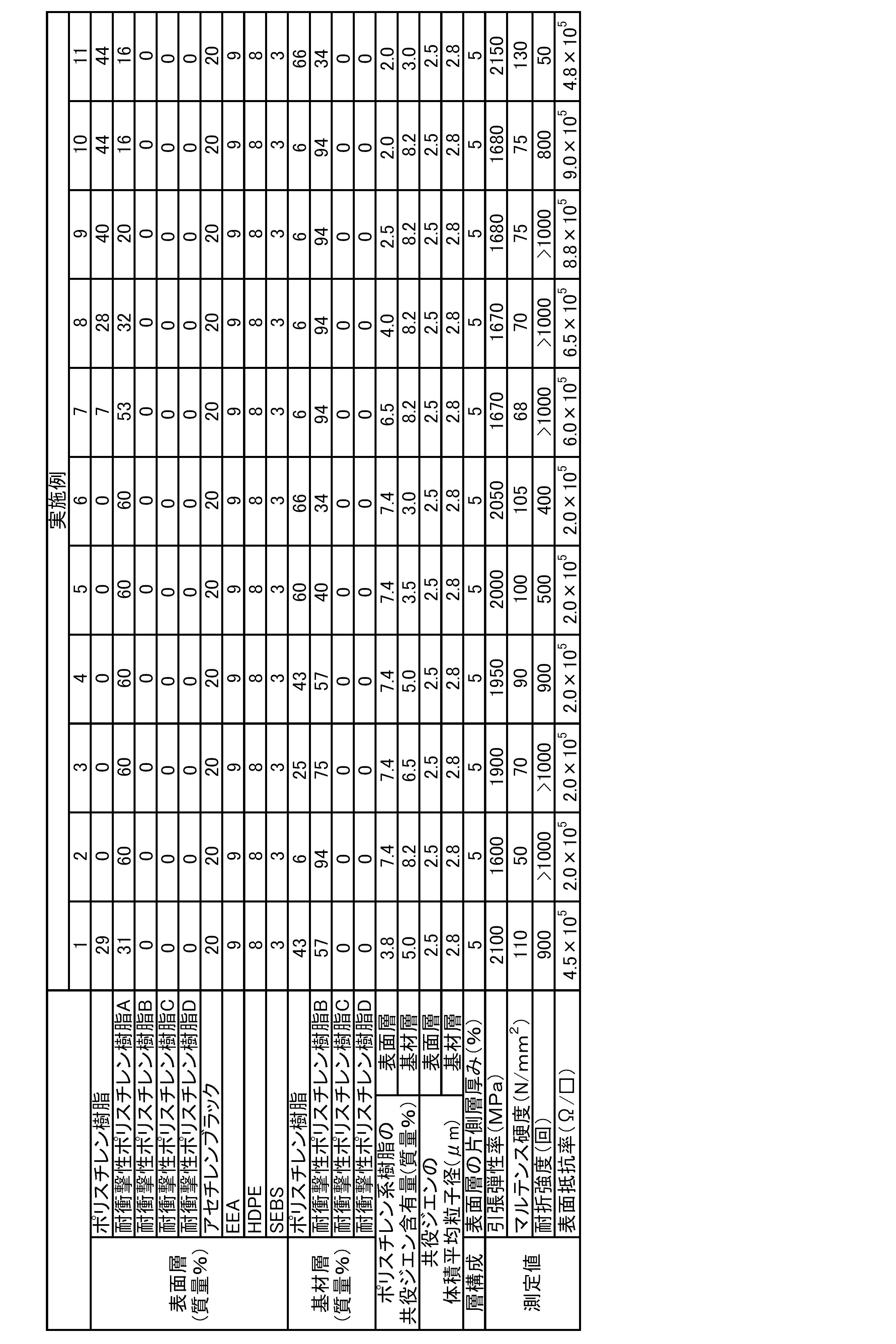
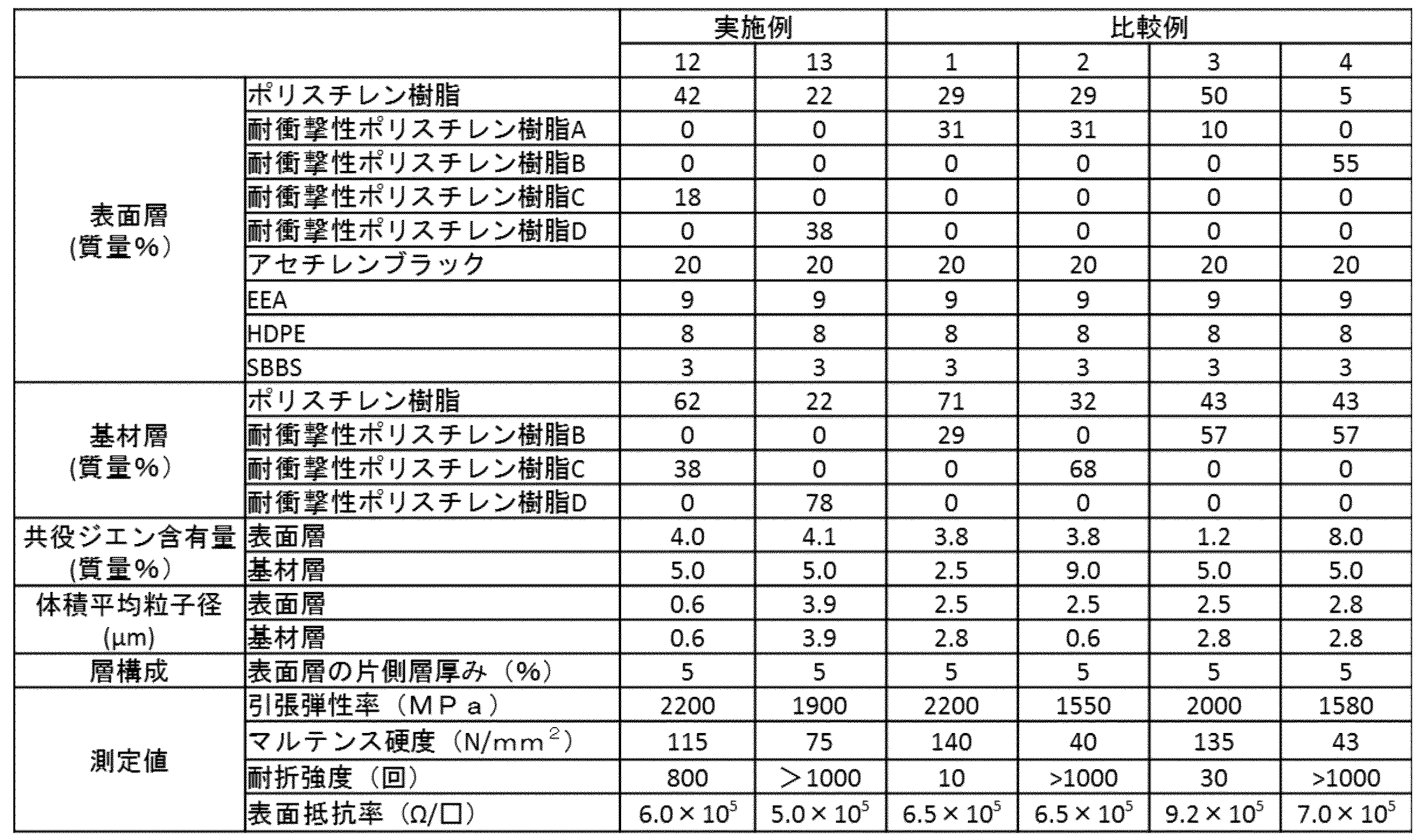
- Examples 2 to 13, Comparative Examples 1 to 4 According to the method of Example 1, a surface conductive laminated sheet was obtained. Tables 2 and 3 show the respective raw materials and the mixing ratio thereof.
- Table 2 and Table 3 collectively show the evaluation results of the sheets prepared in each Example and Comparative Example.
- the surface conductive laminated sheet of each example is a sheet for packaging various electronic components, while ensuring a practically sufficient tensile elastic modulus, folding strength, and surface resistivity, and has a high Martens hardness. It was confirmed that the carrier tape obtained by molding does not crush or deform even when the pickup nozzle contacts. On the other hand, the surface conductive laminated sheets of Comparative Examples 1 and 3 have too high Martens hardness and low bending strength, and the surface conductive laminated sheets of Comparative Examples 2 and 4 have too low Martens hardness. It was confirmed that the carrier tape obtained by molding the sheet was crushed or deformed by contact with the pickup nozzle.
Landscapes
- Engineering & Computer Science (AREA)
- Mechanical Engineering (AREA)
- Packaging Frangible Articles (AREA)
- Laminated Bodies (AREA)
- Wrappers (AREA)
- Packages (AREA)
Abstract
Description
また、表面導電性積層シートの引張弾性率は1600~2200MPa、1650~2100MPa、又は1650~2000MPaであってもよい。
また、表面導電性積層シートの耐折強度は少なくとも50回、少なくとも400回、少なくとも600回、少なくとも800回、又は少なくとも1000回であってもよい。
各評価はシートの押出方向にサンプリングし、次に示す方法によって行った。
(1)マルテンス硬度
シートサンプルについてISO14577に準拠し、東陽テクニカ社製Nano Indenter G200を用いて表面中任意の5点を測定し、その平均値をマルテンス硬度とした。この時、圧子の接近速度500nm/s、最大試験荷重5mNで測定を行った。
(2)引張弾性率
シートサンプルについてJIS-K-7127に準拠し、東洋精機製作所製ストログラフVE―1Dを用いて試験片タイプ5で測定した。
(3)耐折強度
シートサンプルについてJIS-P-8115(2001年)に準拠し、長さ150mm、幅15mm、厚さ0.2mmの試験片を作製し、東洋精機製作所製MIT耐折疲労試験機を用いてMIT耐折強度の測定を行った。この時、折り曲げ角度135度、折り曲げ速度175回毎分、測定荷重250gにて試験を行った。
(4)表面抵抗値
三菱化学アナリテック社製ハイレスタ-UX(MCP-HT800)を用いて測定した。
(5)共役ジエン含有量
耐衝撃ポリスチレン中の共役ジエン含有量はゴム変性ポリスチレンで一般的に用いられている赤外吸収スペクトル法で、960cm-1、910cm-1における吸光度を測定して求めた。
(6)体積平均粒子径
分散粒子の体積平均粒子径は、耐衝撃性ポリスチレン0.5gをジメチルホルムアミド100gに溶解し、日科機社製コールターカウンター(LS-230)を用いて測定した。

カーボンブラックとして、デンカ社製のアセチレンブラック粒状を用いた。
オレフィン系樹脂として、エチレン-アクリル酸エチル共重合体樹脂(以下、EEAという)は、アクリル酸エチル含有量(JIS-K-7192に準じ測定)=18%、メルトフローインデックス(JIS-K-7192に準じ測定)=5.0g/10分のものを用いた。また、高密度ポリエチレン樹脂(以下、HDPEという)は、メルトフローインデックス(JIS-K-6922-2に準じ測定)=0.20g/10分のものを用いた。
芳香族ビニル-共役ジエン系ブロック共重合体の水素添加樹脂として、スチレン-エチレン-ブチレン-スチレンブロック共重合体(以下、SEBSという)は、メルトフローインデックス(JIS-K-7192に準じ測定)=4.0g/10分、スチレンとブタジエンの質量%比率は60:40のものを用いた。
表面層用として、表2に示すようにポリスチレン樹脂と耐衝撃性ポリスチレン樹脂A、カーボンブラック、EEA、HDPE、SEBSを各々29:31:20:9:8:3の割合となるように計量し、高速混合機により均一混合した後、φ45mmベント式二軸押出機を用いて混練し、ストランドカット法によりペレット化し導電性樹脂組成物を得た。
一方、基材層用として、表2に示すようにポリスチレン樹脂及び耐衝撃性ポリスチレン樹脂Bを各々43:57の割合となるように計量し、高速混合機により均一にした混合物を得た。
前記のペレット状の導電性樹脂組成物、及びポリスチレン樹脂と耐衝撃性ポリスチレン樹脂Bとの均一混合物を用い、基材層の両面に表面層がほぼ同じ肉厚となる様に、基材層用としてφ65mm押出機(L/D=28)、表面層用としてφ40mm押出機(L/D=26)及び500mm幅のTダイを用いたフィードブロック法により積層し、表面層と基材層の厚み比率が1:18:1で全体の肉厚が0.2mmとなる表面導電性積層シートを得た。
前記実施例1の方法に従い、表面導電性積層シートを得た。各原料及びそれらの混合割合を表2及び表3に示す。
Claims (7)
- 共役ジエン含有量が3.0~8.2質量%であるポリスチレン系樹脂からなるシート基材層の両面に、共役ジエン含有量が2.0~7.4質量%であるポリスチレン系樹脂、及び導電性フィラーを含む導電性樹脂組成物からなる表面層が積層され、マルテンス硬度が50~130N/mm2である表面導電性積層シート。
- 前記導電性フィラーがカーボンブラックである請求項1に記載の表面導電性積層シート。
- 表面層の導電性樹脂組成物が、オレフィン系樹脂及び芳香族ビニル-共役ジエン系ブロック共重合体の水素添加樹脂をさらに含む、請求項2に記載の表面導電性積層シート。
- 前記表面層が、ポリスチレン系樹脂46~85質量%、カーボンブラック13~23質量%、オレフィン系樹脂1.5~20質量%、及び芳香族ビニル-共役ジエン系ブロック共重合体の水素添加樹脂0.5~11質量%を含有する請求項3に記載の表面導電性積層シート。
- 前記基材層および表面層に用いるポリスチレン系樹脂に含有する共役ジエンの体積平均粒子径が0.5~4.0μmである請求項1から4の何れか一項に記載の表面導電性積層シート。
- 請求項1から5の何れか一項に記載の表面導電性積層シートから成形されてなる電子部品包装容器。
- キャリアテープ又は電子部品搬送用トレイである請求項6に記載の電子部品包装容器。
Priority Applications (6)
| Application Number | Priority Date | Filing Date | Title |
|---|---|---|---|
| KR1020197015027A KR102564612B1 (ko) | 2016-11-01 | 2017-10-31 | 표면 도전성 적층 시트 및 전자 부품 포장 용기 |
| PH1/2019/500955A PH12019500955B1 (en) | 2016-11-01 | 2017-10-31 | Surface-conductive laminated sheet and electronic component packaging container |
| CN201780081734.9A CN110139755B (zh) | 2016-11-01 | 2017-10-31 | 表面导电性叠层片和电子部件包装容器 |
| JP2018549004A JP6686167B2 (ja) | 2016-11-01 | 2017-10-31 | 表面導電性積層シート及び電子部品包装容器 |
| SG11201903634WA SG11201903634WA (en) | 2016-11-01 | 2017-10-31 | Surface-conductive laminated sheet and electronic component packaging container |
| MYPI2019002255A MY193213A (en) | 2016-11-01 | 2017-10-31 | Surface-conductive laminated sheet and electronic component packaging container |
Applications Claiming Priority (2)
| Application Number | Priority Date | Filing Date | Title |
|---|---|---|---|
| JP2016-214012 | 2016-11-01 | ||
| JP2016214012 | 2016-11-01 |
Publications (1)
| Publication Number | Publication Date |
|---|---|
| WO2018084129A1 true WO2018084129A1 (ja) | 2018-05-11 |
Family
ID=62075830
Family Applications (1)
| Application Number | Title | Priority Date | Filing Date |
|---|---|---|---|
| PCT/JP2017/039258 Ceased WO2018084129A1 (ja) | 2016-11-01 | 2017-10-31 | 表面導電性積層シート及び電子部品包装容器 |
Country Status (8)
| Country | Link |
|---|---|
| JP (2) | JP6686167B2 (ja) |
| KR (1) | KR102564612B1 (ja) |
| CN (1) | CN110139755B (ja) |
| MY (1) | MY193213A (ja) |
| PH (1) | PH12019500955B1 (ja) |
| SG (1) | SG11201903634WA (ja) |
| TW (1) | TWI738905B (ja) |
| WO (1) | WO2018084129A1 (ja) |
Cited By (6)
| Publication number | Priority date | Publication date | Assignee | Title |
|---|---|---|---|---|
| WO2020218133A1 (ja) * | 2019-04-26 | 2020-10-29 | デンカ株式会社 | 積層シート及び電子部品包装容器並びに電子部品包装体 |
| CN114667218A (zh) * | 2020-03-19 | 2022-06-24 | 电化株式会社 | 层叠片材、容器、载带及电子部件包装体 |
| JP2023515346A (ja) * | 2020-05-19 | 2023-04-13 | ハンファ ソリューションズ コーポレーション | 粘着性及び電気伝導性に優れた多層成形品及びそれにより移送される電子製品 |
| JP2023086539A (ja) * | 2021-12-10 | 2023-06-22 | デンカ株式会社 | 樹脂シート及び成形容器 |
| JPWO2023189186A1 (ja) * | 2022-03-28 | 2023-10-05 | ||
| WO2023189190A1 (ja) * | 2022-03-28 | 2023-10-05 | デンカ株式会社 | 樹脂シート、容器、キャリアテープ、及び電子部品包装体 |
Families Citing this family (3)
| Publication number | Priority date | Publication date | Assignee | Title |
|---|---|---|---|---|
| EP4112293A4 (en) * | 2020-02-27 | 2024-03-20 | Junkosha Inc. | MULTI-LAYER HOSE |
| WO2022201873A1 (ja) * | 2021-03-22 | 2022-09-29 | デンカ株式会社 | 電子部品包装用樹脂シート及びそれを用いた電子部品包装容器 |
| EP4678396A1 (en) * | 2023-03-06 | 2026-01-14 | Denka Company Limited | Sheet having base material layer containing abs-based resin |
Citations (9)
| Publication number | Priority date | Publication date | Assignee | Title |
|---|---|---|---|---|
| JP2003073541A (ja) * | 2001-06-22 | 2003-03-12 | Denki Kagaku Kogyo Kk | 導電性樹脂組成物 |
| JP2004276479A (ja) * | 2003-03-18 | 2004-10-07 | Sumitomo Bakelite Co Ltd | 表面導電性複合プラスチックシート及び電子部品搬送用容器 |
| US20050250897A1 (en) * | 2004-03-03 | 2005-11-10 | Chi Lin Technology Co., Ltd. | Conductive plastic composition |
| WO2006030871A1 (ja) * | 2004-09-16 | 2006-03-23 | Denki Kagaku Kogyo Kabushiki Kaisha | 複合シート |
| JP2006150729A (ja) * | 2004-11-29 | 2006-06-15 | Dainippon Ink & Chem Inc | 導電性シート及び成形品 |
| JP2006212851A (ja) * | 2005-02-02 | 2006-08-17 | Denki Kagaku Kogyo Kk | 熱可塑性樹脂積層シート及びその成形体 |
| JP2006231542A (ja) * | 2005-02-22 | 2006-09-07 | Dainippon Ink & Chem Inc | 帯電防止性積層シート及びその成形品 |
| WO2012046815A1 (ja) * | 2010-10-07 | 2012-04-12 | 電気化学工業株式会社 | 電子部品包装用シート及びその成形体 |
| WO2012102287A1 (ja) * | 2011-01-28 | 2012-08-02 | 電気化学工業株式会社 | 電子部品包装用積層シート及びその成形体 |
Family Cites Families (9)
| Publication number | Priority date | Publication date | Assignee | Title |
|---|---|---|---|---|
| JP3209394B2 (ja) | 1995-09-19 | 2001-09-17 | 電気化学工業株式会社 | 導電性複合プラスチックシート及び容器 |
| JP3276818B2 (ja) | 1995-09-19 | 2002-04-22 | 電気化学工業株式会社 | 導電性複合プラスチックシート及び容器 |
| JP3381488B2 (ja) * | 1995-11-06 | 2003-02-24 | 三菱化学株式会社 | 熱可塑性エラストマー組成物及び複合成形体 |
| JP3190241B2 (ja) | 1995-12-21 | 2001-07-23 | 電気化学工業株式会社 | 電子部品包装用導電性複合プラスチックシート及び容器 |
| US20040115381A1 (en) * | 2002-12-12 | 2004-06-17 | Chevron Phillips Chemical Company, Lp | Method for manufacturing articles with materials containing tapered polymers |
| EP1787804B1 (en) * | 2004-09-07 | 2011-04-20 | Denki Kagaku Kogyo Kabushiki Kaisha | Conductive composite sheeting |
| US20110008561A1 (en) * | 2007-12-26 | 2011-01-13 | Denki Kagaku Kogyo Kabushiki Kaisha | Sheet for packaging electronic part |
| WO2009126366A2 (en) * | 2008-04-10 | 2009-10-15 | World Properties, Inc. | Circuit materials with improved bond, method of manufacture thereof, and articles formed therefrom |
| CN104960292B (zh) * | 2015-06-17 | 2017-01-25 | 浙江洁美电子科技股份有限公司 | 电子元器件收纳载带的封装带及其制备方法 |
-
2017
- 2017-10-31 JP JP2018549004A patent/JP6686167B2/ja active Active
- 2017-10-31 WO PCT/JP2017/039258 patent/WO2018084129A1/ja not_active Ceased
- 2017-10-31 PH PH1/2019/500955A patent/PH12019500955B1/en unknown
- 2017-10-31 CN CN201780081734.9A patent/CN110139755B/zh active Active
- 2017-10-31 KR KR1020197015027A patent/KR102564612B1/ko active Active
- 2017-10-31 MY MYPI2019002255A patent/MY193213A/en unknown
- 2017-10-31 SG SG11201903634WA patent/SG11201903634WA/en unknown
- 2017-11-01 TW TW106137687A patent/TWI738905B/zh active
-
2020
- 2020-04-01 JP JP2020065632A patent/JP2020114675A/ja active Pending
Patent Citations (9)
| Publication number | Priority date | Publication date | Assignee | Title |
|---|---|---|---|---|
| JP2003073541A (ja) * | 2001-06-22 | 2003-03-12 | Denki Kagaku Kogyo Kk | 導電性樹脂組成物 |
| JP2004276479A (ja) * | 2003-03-18 | 2004-10-07 | Sumitomo Bakelite Co Ltd | 表面導電性複合プラスチックシート及び電子部品搬送用容器 |
| US20050250897A1 (en) * | 2004-03-03 | 2005-11-10 | Chi Lin Technology Co., Ltd. | Conductive plastic composition |
| WO2006030871A1 (ja) * | 2004-09-16 | 2006-03-23 | Denki Kagaku Kogyo Kabushiki Kaisha | 複合シート |
| JP2006150729A (ja) * | 2004-11-29 | 2006-06-15 | Dainippon Ink & Chem Inc | 導電性シート及び成形品 |
| JP2006212851A (ja) * | 2005-02-02 | 2006-08-17 | Denki Kagaku Kogyo Kk | 熱可塑性樹脂積層シート及びその成形体 |
| JP2006231542A (ja) * | 2005-02-22 | 2006-09-07 | Dainippon Ink & Chem Inc | 帯電防止性積層シート及びその成形品 |
| WO2012046815A1 (ja) * | 2010-10-07 | 2012-04-12 | 電気化学工業株式会社 | 電子部品包装用シート及びその成形体 |
| WO2012102287A1 (ja) * | 2011-01-28 | 2012-08-02 | 電気化学工業株式会社 | 電子部品包装用積層シート及びその成形体 |
Cited By (12)
| Publication number | Priority date | Publication date | Assignee | Title |
|---|---|---|---|---|
| WO2020218133A1 (ja) * | 2019-04-26 | 2020-10-29 | デンカ株式会社 | 積層シート及び電子部品包装容器並びに電子部品包装体 |
| JPWO2020218133A1 (ja) * | 2019-04-26 | 2020-10-29 | ||
| US11701874B2 (en) | 2019-04-26 | 2023-07-18 | Denka Company Limited | Layered sheet, electronic component packaging container, and electronic component packaging |
| JP7442509B2 (ja) | 2019-04-26 | 2024-03-04 | デンカ株式会社 | 積層シート及び電子部品包装容器並びに電子部品包装体 |
| CN114667218A (zh) * | 2020-03-19 | 2022-06-24 | 电化株式会社 | 层叠片材、容器、载带及电子部件包装体 |
| US12154818B2 (en) | 2020-03-19 | 2024-11-26 | Denka Company Limited | Layered sheet, container, carrier tape, and electronic component packaging body |
| JP2023515346A (ja) * | 2020-05-19 | 2023-04-13 | ハンファ ソリューションズ コーポレーション | 粘着性及び電気伝導性に優れた多層成形品及びそれにより移送される電子製品 |
| JP2023086539A (ja) * | 2021-12-10 | 2023-06-22 | デンカ株式会社 | 樹脂シート及び成形容器 |
| JPWO2023189186A1 (ja) * | 2022-03-28 | 2023-10-05 | ||
| WO2023189190A1 (ja) * | 2022-03-28 | 2023-10-05 | デンカ株式会社 | 樹脂シート、容器、キャリアテープ、及び電子部品包装体 |
| JPWO2023189190A1 (ja) * | 2022-03-28 | 2023-10-05 | ||
| JP7805442B2 (ja) | 2022-03-28 | 2026-01-23 | デンカ株式会社 | 樹脂シート、容器、キャリアテープ、及び電子部品包装体 |
Also Published As
| Publication number | Publication date |
|---|---|
| JP6686167B2 (ja) | 2020-04-22 |
| TWI738905B (zh) | 2021-09-11 |
| KR102564612B1 (ko) | 2023-08-07 |
| MY193213A (en) | 2022-09-26 |
| KR20190078599A (ko) | 2019-07-04 |
| CN110139755B (zh) | 2021-04-09 |
| CN110139755A (zh) | 2019-08-16 |
| SG11201903634WA (en) | 2019-05-30 |
| PH12019500955B1 (en) | 2023-11-22 |
| JP2020114675A (ja) | 2020-07-30 |
| PH12019500955A1 (en) | 2019-12-02 |
| TW201829197A (zh) | 2018-08-16 |
| JPWO2018084129A1 (ja) | 2019-09-19 |
Similar Documents
| Publication | Publication Date | Title |
|---|---|---|
| JP6686167B2 (ja) | 表面導電性積層シート及び電子部品包装容器 | |
| KR101868178B1 (ko) | 전자 부품 포장용 시트 및 이의 성형체 | |
| JPWO2008020579A1 (ja) | 導電性樹脂組成物、及びそれを用いた導電性シート | |
| JP2024161037A (ja) | 積層シート、容器、キャリアテープ、及び電子部品包装体 | |
| JP3209394B2 (ja) | 導電性複合プラスチックシート及び容器 | |
| TWI402166B (zh) | 複合薄片 | |
| HK1049348A1 (zh) | 導電樹脂組合物 | |
| JP5259131B2 (ja) | 樹脂組成物、及びシート | |
| CN101014463B (zh) | 导电性复合片材 | |
| JP3209393B2 (ja) | 導電性複合プラスチックシート及び容器 | |
| JP4163620B2 (ja) | 電子部品包装用多層シート | |
| JP7158388B2 (ja) | 導電性樹脂組成物 | |
| TW202103961A (zh) | 積層薄片及電子零件包裝容器以及電子零件包裝體 | |
| JP3202553B2 (ja) | 導電性複合プラスチックシート及び容器 | |
| JPH1120069A (ja) | 導電性複合プラスチックシート | |
| JP2001334611A (ja) | 導電性複合プラスチックシート及び容器 | |
| JP4360111B2 (ja) | 表面導電性複合プラスチックシート及び電子部品搬送用容器 | |
| KR20240164924A (ko) | 수지 시트, 용기, 캐리어 테이프 및 전자 부품 포장체 | |
| KR20240163128A (ko) | 수지 시트, 용기, 캐리어 테이프 및 전자 부품 포장체 | |
| JP2006212851A (ja) | 熱可塑性樹脂積層シート及びその成形体 | |
| JP2004276479A (ja) | 表面導電性複合プラスチックシート及び電子部品搬送用容器 | |
| JP3324682B2 (ja) | 導電性複合プラスチックシートの製造法 | |
| JP2020176205A (ja) | 帯電防止成形材料、帯電防止シート、及び、帯電防止エンボスキャリアテープ | |
| JP2001315265A (ja) | 導電性複合プラスチックシート及び容器 |
Legal Events
| Date | Code | Title | Description |
|---|---|---|---|
| 121 | Ep: the epo has been informed by wipo that ep was designated in this application |
Ref document number: 17867304 Country of ref document: EP Kind code of ref document: A1 |
|
| ENP | Entry into the national phase |
Ref document number: 2018549004 Country of ref document: JP Kind code of ref document: A |
|
| NENP | Non-entry into the national phase |
Ref country code: DE |
|
| ENP | Entry into the national phase |
Ref document number: 20197015027 Country of ref document: KR Kind code of ref document: A |
|
| 122 | Ep: pct application non-entry in european phase |
Ref document number: 17867304 Country of ref document: EP Kind code of ref document: A1 |