WO2018056357A1 - 半導体装置およびその製造方法 - Google Patents
半導体装置およびその製造方法 Download PDFInfo
- Publication number
- WO2018056357A1 WO2018056357A1 PCT/JP2017/034101 JP2017034101W WO2018056357A1 WO 2018056357 A1 WO2018056357 A1 WO 2018056357A1 JP 2017034101 W JP2017034101 W JP 2017034101W WO 2018056357 A1 WO2018056357 A1 WO 2018056357A1
- Authority
- WO
- WIPO (PCT)
- Prior art keywords
- layer
- type
- forming
- conductivity type
- jfet portion
- Prior art date
- Legal status (The legal status is an assumption and is not a legal conclusion. Google has not performed a legal analysis and makes no representation as to the accuracy of the status listed.)
- Ceased
Links
Images


Classifications
-
- H—ELECTRICITY
- H10—SEMICONDUCTOR DEVICES; ELECTRIC SOLID-STATE DEVICES NOT OTHERWISE PROVIDED FOR
- H10D—INORGANIC ELECTRIC SEMICONDUCTOR DEVICES
- H10D30/00—Field-effect transistors [FET]
- H10D30/60—Insulated-gate field-effect transistors [IGFET]
- H10D30/64—Double-diffused metal-oxide semiconductor [DMOS] FETs
- H10D30/66—Vertical DMOS [VDMOS] FETs
- H10D30/668—Vertical DMOS [VDMOS] FETs having trench gate electrodes, e.g. UMOS transistors
-
- H—ELECTRICITY
- H10—SEMICONDUCTOR DEVICES; ELECTRIC SOLID-STATE DEVICES NOT OTHERWISE PROVIDED FOR
- H10D—INORGANIC ELECTRIC SEMICONDUCTOR DEVICES
- H10D12/00—Bipolar devices controlled by the field effect, e.g. insulated-gate bipolar transistors [IGBT]
- H10D12/01—Manufacture or treatment
- H10D12/031—Manufacture or treatment of IGBTs
-
- H—ELECTRICITY
- H10—SEMICONDUCTOR DEVICES; ELECTRIC SOLID-STATE DEVICES NOT OTHERWISE PROVIDED FOR
- H10D—INORGANIC ELECTRIC SEMICONDUCTOR DEVICES
- H10D62/00—Semiconductor bodies, or regions thereof, of devices having potential barriers
- H10D62/10—Shapes, relative sizes or dispositions of the regions of the semiconductor bodies; Shapes of the semiconductor bodies
- H10D62/102—Constructional design considerations for preventing surface leakage or controlling electric field concentration
- H10D62/103—Constructional design considerations for preventing surface leakage or controlling electric field concentration for increasing or controlling the breakdown voltage of reverse-biased devices
- H10D62/105—Constructional design considerations for preventing surface leakage or controlling electric field concentration for increasing or controlling the breakdown voltage of reverse-biased devices by having particular doping profiles, shapes or arrangements of PN junctions; by having supplementary regions, e.g. junction termination extension [JTE]
- H10D62/109—Reduced surface field [RESURF] PN junction structures
- H10D62/111—Multiple RESURF structures, e.g. double RESURF or 3D-RESURF structures
-
- H—ELECTRICITY
- H10—SEMICONDUCTOR DEVICES; ELECTRIC SOLID-STATE DEVICES NOT OTHERWISE PROVIDED FOR
- H10D—INORGANIC ELECTRIC SEMICONDUCTOR DEVICES
- H10D62/00—Semiconductor bodies, or regions thereof, of devices having potential barriers
- H10D62/10—Shapes, relative sizes or dispositions of the regions of the semiconductor bodies; Shapes of the semiconductor bodies
- H10D62/13—Semiconductor regions connected to electrodes carrying current to be rectified, amplified or switched, e.g. source or drain regions
- H10D62/149—Source or drain regions of field-effect devices
- H10D62/151—Source or drain regions of field-effect devices of IGFETs
- H10D62/156—Drain regions of DMOS transistors
- H10D62/157—Impurity concentrations or distributions
-
- H—ELECTRICITY
- H10—SEMICONDUCTOR DEVICES; ELECTRIC SOLID-STATE DEVICES NOT OTHERWISE PROVIDED FOR
- H10D—INORGANIC ELECTRIC SEMICONDUCTOR DEVICES
- H10D62/00—Semiconductor bodies, or regions thereof, of devices having potential barriers
- H10D62/10—Shapes, relative sizes or dispositions of the regions of the semiconductor bodies; Shapes of the semiconductor bodies
- H10D62/13—Semiconductor regions connected to electrodes carrying current to be rectified, amplified or switched, e.g. source or drain regions
- H10D62/149—Source or drain regions of field-effect devices
- H10D62/151—Source or drain regions of field-effect devices of IGFETs
- H10D62/156—Drain regions of DMOS transistors
- H10D62/159—Shapes
-
- H—ELECTRICITY
- H10—SEMICONDUCTOR DEVICES; ELECTRIC SOLID-STATE DEVICES NOT OTHERWISE PROVIDED FOR
- H10D—INORGANIC ELECTRIC SEMICONDUCTOR DEVICES
- H10D62/00—Semiconductor bodies, or regions thereof, of devices having potential barriers
- H10D62/10—Shapes, relative sizes or dispositions of the regions of the semiconductor bodies; Shapes of the semiconductor bodies
- H10D62/17—Semiconductor regions connected to electrodes not carrying current to be rectified, amplified or switched, e.g. channel regions
- H10D62/393—Body regions of DMOS transistors or IGBTs
-
- H—ELECTRICITY
- H10—SEMICONDUCTOR DEVICES; ELECTRIC SOLID-STATE DEVICES NOT OTHERWISE PROVIDED FOR
- H10D—INORGANIC ELECTRIC SEMICONDUCTOR DEVICES
- H10D62/00—Semiconductor bodies, or regions thereof, of devices having potential barriers
- H10D62/80—Semiconductor bodies, or regions thereof, of devices having potential barriers characterised by the materials
- H10D62/83—Semiconductor bodies, or regions thereof, of devices having potential barriers characterised by the materials being Group IV materials, e.g. B-doped Si or undoped Ge
- H10D62/832—Semiconductor bodies, or regions thereof, of devices having potential barriers characterised by the materials being Group IV materials, e.g. B-doped Si or undoped Ge being Group IV materials comprising two or more elements, e.g. SiGe
- H10D62/8325—Silicon carbide
-
- H—ELECTRICITY
- H10—SEMICONDUCTOR DEVICES; ELECTRIC SOLID-STATE DEVICES NOT OTHERWISE PROVIDED FOR
- H10D—INORGANIC ELECTRIC SEMICONDUCTOR DEVICES
- H10D64/00—Electrodes of devices having potential barriers
- H10D64/20—Electrodes characterised by their shapes, relative sizes or dispositions
- H10D64/23—Electrodes carrying the current to be rectified, amplified, oscillated or switched, e.g. sources, drains, anodes or cathodes
- H10D64/251—Source or drain electrodes for field-effect devices
- H10D64/256—Source or drain electrodes for field-effect devices for lateral devices wherein the source or drain electrodes are recessed in semiconductor bodies
-
- H—ELECTRICITY
- H10—SEMICONDUCTOR DEVICES; ELECTRIC SOLID-STATE DEVICES NOT OTHERWISE PROVIDED FOR
- H10P—GENERIC PROCESSES OR APPARATUS FOR THE MANUFACTURE OR TREATMENT OF DEVICES COVERED BY CLASS H10
- H10P95/00—Generic processes or apparatus for manufacture or treatments not covered by the other groups of this subclass
- H10P95/90—Thermal treatments, e.g. annealing or sintering
Definitions
- the present disclosure relates to a semiconductor device and a manufacturing method thereof, and is particularly suitable when applied to a semiconductor element using a wide band gap semiconductor such as silicon carbide (hereinafter referred to as SiC) and a manufacturing method thereof.
- SiC silicon carbide
- a reduction in on-resistance value is necessary to reduce switching loss, but the value of a current flowing through a semiconductor element when a load is short-circuited increases in inverse proportion to the on-resistance value of the semiconductor element. That is, the smaller the on-resistance value, the larger the saturation current when the load is short-circuited. As a result, the semiconductor element is easily damaged by self-heating, so that the tolerance of the SiC semiconductor device when the load is short-circuited is lowered. For this reason, there is a trade-off relationship between reducing the on-resistance value and improving the withstand capability of the SiC semiconductor device when the load is short-circuited. However, this trade-off relationship is improved, that is, both the low on-resistance value and the low saturation current are compatible. Is desired.
- Patent Document 1 in order to achieve both a low on-resistance value and a low saturation current, the impurity concentration in the vicinity of the channel in the p-type base region is different from the impurity concentration in the JFET portion.
- the impurity concentration of the p-type base region is graded in the depth direction so that the impurity concentration is low in the vicinity of the channel and increases as it goes downward. According to such a configuration, since the impurity concentration of the p-type base region is lowered in the vicinity of the channel, a low on-resistance can be realized.
- the JFET portion in the p-type base region can be pinched off, and a low saturation current can be realized. Therefore, it is possible to achieve both a low on-resistance value and a low saturation current.
- the impurity concentration of the JFET portion in the p-type base region is increased or the adjacent p-type base region in the JFET portion so as to obtain a high withstand amount as a lower saturation current. Narrowing the interval increases the JFET resistance. For this reason, it becomes impossible to achieve both a low on-resistance value and a low saturation current.
- An SiC semiconductor device includes a first or second conductivity type substrate made of a semiconductor, and a first conductivity type semiconductor formed on the substrate and having a lower impurity concentration than the substrate.
- a drift layer comprising: a second conductivity type region comprising a second conductivity type semiconductor formed on the drift layer; and a JFET portion formed on the drift layer and disposed between the second conductivity type regions.
- the formed gate insulating film, the gate electrode formed on the gate insulating film, the interlayer insulating film covering the gate electrode and the gate insulating film and having the contact hole formed therein, and the source region through the contact hole A source electrode electrically connected, and is configured having a drain electrode formed on the back surface side of the substrate. Specifically, a channel region is formed by applying a gate voltage to the gate electrode and a normal operation voltage as a drain voltage to be applied to the drain electrode, and via the source region and the JFET part. , An inversion type semiconductor element in which a current flows between the source electrode and the drain electrode.
- the amount of extension of the depletion layer extending from the second conductivity type region to the JFET portion when the normal operation voltage is applied as the drain voltage between the JFET portion and the second conductivity type region is formed that pinches off the JFET portion by the depletion layer when a current is passed through the JFET portion while being suppressed and a voltage higher than the normal operation voltage is applied as the drain voltage.
- a depletion layer adjusting layer is formed at least on the side surface of the deep layer, that is, between the deep layer and the JFET portion. For this reason, during normal operation, the depletion layer adjustment layer functions as a layer that adjusts the extension of the depletion layer, it is possible to suppress the extension of the depletion layer into the JFET portion, and the current path is narrowed. Since it can suppress, it becomes possible to aim at a low on-resistance.
- the depletion layer extending from the deep layer side to the depletion layer adjustment layer extends beyond the thickness of the depletion layer adjustment layer, and the JFET portion is immediately pinched off. .
- a low saturation current can be maintained, and the tolerance of the SiC semiconductor device due to a load short circuit or the like can be improved. Therefore, it is possible to provide a SiC semiconductor device that can achieve both a low on-resistance value and a low saturation current.
- FIG. 3 is a cross-sectional view showing a manufacturing process of the SiC semiconductor device shown in FIG. 1.
- FIG. 5B is a cross-sectional view showing a manufacturing step of the SiC semiconductor device following FIG. 5A.
- FIG. 5B is a cross-sectional view showing a manufacturing step of the SiC semiconductor device following FIG. 5B.
- FIG. 5D is a cross-sectional view showing a manufacturing step of the SiC semiconductor device following FIG.
- FIG. 5D is a cross-sectional view showing a manufacturing step of the SiC semiconductor device following FIG. 5D.
- FIG. 5E is a cross-sectional view showing a manufacturing step of the SiC semiconductor device following FIG. 5E.
- FIG. 5F is a cross-sectional view showing a manufacturing step of the SiC semiconductor device following FIG. 5F.
- FIG. 5G is a cross-sectional view showing a manufacturing step of the SiC semiconductor device following FIG. 5G.
- FIG. 5H is a cross-sectional view showing a manufacturing step of the SiC semiconductor device following FIG. 5H.
- FIG. 5F is a cross sectional view showing a manufacturing step of the SiC semiconductor device following FIG.
- FIG. 15B is a cross-sectional view showing a manufacturing step of the SiC semiconductor device following FIG. 15A.
- FIG. 15B is a cross-sectional view showing a manufacturing step of the SiC semiconductor device following FIG. 15B.
- FIG. 15D is a cross-sectional view showing a manufacturing step of the SiC semiconductor device following FIG. 15C.
- FIG. 16B is a cross-sectional view showing a manufacturing step of the SiC semiconductor device following FIG. 16A.
- FIG. 16B is a cross-sectional view showing a manufacturing step of the SiC semiconductor device following FIG. 16B.
- FIG. 16D is a cross-sectional view showing a manufacturing step of the SiC semiconductor device following FIG. 16C.
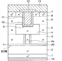
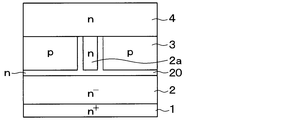
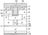
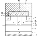
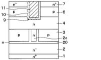
- the SiC semiconductor device according to the present embodiment has a vertical MOSFET formed as a semiconductor element.
- the vertical MOSFET is formed in the cell region of the SiC semiconductor device, and the SiC semiconductor device is configured by forming the outer peripheral breakdown voltage structure so as to surround the cell region. Only shown.
- the horizontal direction in FIG. 1 is the width direction
- the vertical direction is the thickness direction or depth direction.
- an n + type substrate 1 made of SiC is used as a semiconductor substrate.
- An n ⁇ type drift layer 2 made of SiC is formed on the main surface of n + type substrate 1.
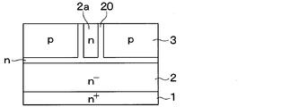
- the n ⁇ type drift layer 2 is connected to a narrow JFET portion 2a at a position away from the n + type substrate 1, and a p-type deep layer 3 made of SiC is formed on both sides of the JFET portion 2a.
- the JFET portion 2a has a strip shape extending along the longitudinal direction of a trench gate structure described later, and the periphery of the JFET portion 2a is a p-type deep layer 3.
- a high concentration n-type layer 20 is formed between the n ⁇ -type drift layer 2 and the JFET portion 2 a and the p-type deep layer 3.
- the high concentration n-type layer 20 functions as a depletion layer adjustment layer. More specifically, the high concentration n-type layer 20 is formed at least on the side surface of the p-type deep layer 3, that is, between the p-type deep layer 3 and the JFET portion 2a.
- n - top type drift layer 2 i.e. n - or between n the bottom of the type drift layer 2 and the p-type deep layer 3 - boundary between JFET portion 2a of the type drift layer 2
- a high-concentration n-type layer 20 is also formed at the position.
- the n + type substrate 1 has a (0001) Si surface on the surface, for example, an n type impurity concentration of 5.9 ⁇ 10 18 / cm 3, and a thickness of 100 ⁇ m.
- the n ⁇ -type drift layer 2 has an n-type impurity concentration of 1.0 ⁇ 10 16 / cm 3 and a thickness of 8.0 ⁇ m.
- the n-type impurity concentration is 1.0 ⁇ 10 16 / cm 3 and the width is 0.1 ⁇ m.
- the p-type deep layer 3 has a p-type impurity concentration of 1.0 ⁇ 10 18 / cm 3 and a thickness of 1.0 ⁇ m.
- the high-concentration n-type layer 20 has a higher concentration than the n ⁇ -type drift layer 2 and has an n-type impurity concentration of 1.0 ⁇ 10 18 / cm 3 , for example.
- the thickness of the high-concentration n-type layer 20 is 0.05 ⁇ m on the side surface of the p-type deep layer 3 and 0.07 ⁇ m on the upper surface of the n ⁇ -type drift layer 2.
- an n-type current distribution layer 4 made of SiC connected to the JFET portion 2a and wider than the JFET portion 2a is formed on the JFET portion 2a and the p-type deep layer 3. Further, on the p-type deep layer 3, a p-type coupling layer 5 made of SiC having a width narrower than that of the p-type deep layer 3 is formed.
- the n-type current distribution layer 4 is a layer that allows a current flowing through the channel to diffuse in the width direction, and has a higher concentration than the JFET portion 2a.
- the n-type impurity concentration is 3 ⁇ 10. 17 / cm 3 and a thickness of 0.6 ⁇ m.
- the p-type coupling layer 5 may have the same concentration as the p-type deep layer 3, but in this embodiment, the p-type coupling layer 5 has a higher concentration than the p-type deep layer 3.
- the p-type impurity concentration is 3 ⁇ 10 6. 17 / cm 3 and a thickness of 0.6 ⁇ m.
- a p-type base region 6 made of SiC is formed on the n-type current spreading layer 4 and the p-type coupling layer 5, and the p-type base region 6, the p-type deep layer 3, and the like are interposed via the p-type coupling layer 5.
- An n + type source region 7 and a p + type contact region 8 made of SiC are formed on the p type base region 6.
- the n + type source region 7 is formed on a portion of the p type base region 6 corresponding to the n type current spreading layer 4, and the p + type contact region 8 is a p type of the p type base region 6. It is formed on a portion corresponding to the coupling layer 5.
- the p-type base region 6 is thinner than the p-type deep layer 3 and has a lower p-type impurity concentration.
- the p-type impurity concentration is 3 ⁇ 10 17 / cm 3 and the thickness is 0. .3 ⁇ m.
- the n + -type source region 7 has an n-type impurity concentration higher than that of the n-type current distribution layer 4, and the p + -type contact region 8 has a p-type impurity concentration higher than that of the p-type base region 6. High concentration.
- the width is 0.8 ⁇ m and the depth is p-type base region 6 and the n + -type source region so as to pass through p-type base region 6 and n + -type source region 7 and reach n-type current spreading layer 4.
- the gate trench 9 is formed 0.2 to 0.4 ⁇ m deeper than the total film thickness 7.
- the p-type base region 6 and the n + -type source region 7 are arranged so as to be in contact with the side surface of the gate trench 9.
- the gate trench 9 is formed in a line layout in which the horizontal direction in FIG. 1 is the width direction, the normal direction is the longitudinal direction, and the vertical direction is the depth direction. Although only one gate trench 9 is shown in FIG.
- a plurality of gate trenches 9 are arranged at equal intervals in the left-right direction on the page, and are arranged so as to be sandwiched between the p-type deep layers 3, respectively. It is made into a shape.
- the cell pitch that is the pitch of the gate trench 9, that is, the half cell pitch that is half of the arrangement interval of the adjacent gate trenches 9 is, for example, 1.55 ⁇ m.
- the width of the gate trench 9 is arbitrary, but is smaller than the half cell pitch.
- a portion of the p-type base region 6 located on the side surface of the gate trench 9 is used as a channel region that connects the n + -type source region 7 and the n-type current spreading layer 4 when the vertical MOSFET is operated.
- a gate insulating film 10 is formed on the inner wall surface of the gate trench 9 including the channel region.
- a gate electrode 11 made of doped Poly-Si is formed on the surface of the gate insulating film 10, and the gate trench 9 is completely filled with the gate insulating film 10 and the gate electrode 11.
- a source electrode 13 and the like are formed on the surface of the n + type source region 7 and the p + type contact region 8 and the surface of the gate electrode 11 with an interlayer insulating film 12 interposed therebetween.
- the source electrode 13 is composed of a plurality of metals, such as Ni / Al. Of the plurality of metals, at least the n-type SiC, specifically, the n + -type source region 7 or the portion in contact with the gate electrode 11 in the case of n-type doping is made of a metal capable of ohmic contact with the n-type SiC. Yes.
- the p + -type contact region 8 is made of a metal that can make ohmic contact with the p-type SiC.
- the source electrode 13 is electrically insulated by being formed on the interlayer insulating film 12. The source electrode 13 is in electrical contact with the n + type source region 7 and the p + type contact region 8 through a contact hole formed in the interlayer insulating film 12.
- n + -type substrate 1 On the back side of the n + -type substrate 1 n + -type substrate 1 and electrically connected to the drain electrode 14 are formed.
- an n-channel type inverted MOSFET having a trench gate structure is formed.
- a cell region is configured by arranging a plurality of such vertical MOSFETs.
- An SiC semiconductor device is configured by forming an outer peripheral breakdown voltage structure such as a guard ring (not shown) so as to surround a cell region where such a vertical MOSFET is formed.
- the SiC semiconductor device having the vertical MOSFET configured as described above has a gate voltage Vg of 20 V, for example, with respect to the gate electrode 11 in a state where the source voltage Vs is 0 V and the drain voltage Vd is 1 to 1.5 V, for example. It is operated by applying it. That is, when the gate voltage is applied, the vertical MOSFET performs an operation in which a channel region is formed in the p-type base region 6 in contact with the gate trench 9 and a current flows between the drain and the source.
- the high-concentration n-type layer 20 is disposed at least between the JFET portion 2a and the p-type deep layer 3, the high-concentration n-type layer 20 functions as a depletion layer adjustment layer, so that Will be performed.
- the drain voltage Vd is a voltage applied during normal operation such as 1 to 1.5 V
- a high concentration is applied from the p-type deep layer 3 side.
- the depletion layer extending to the n-type layer 20 extends only with a width smaller than the thickness of the high-concentration n-type layer 20. That is, the high-concentration n-type layer 20 functions as a layer that stops the extension of the depletion layer. For this reason, it is possible to suppress the depletion layer from extending into the JFET portion 2a, and it is possible to suppress the current path from being narrowed, thereby achieving a low on-resistance.
- the portion of the high concentration n-type layer 20 where the depletion layer is not extended functions as a current path. Since the high-concentration n-type layer 20 has an n-type impurity concentration higher than that of the JFET portion 2a and has a low resistance, the high-concentration n-type layer 20 functions as a current path. Further, it is possible to reduce the on-resistance.
- the depletion layer extending from the p-type deep layer 3 side to the high-concentration n-type layer 20 extends beyond the thickness of the high-concentration n-type layer 20. Then, the JFET portion 2a is immediately pinched off prior to the n-type current spreading layer 4. At this time, the relationship between the drain voltage Vd and the width of the depletion layer is determined based on the thickness of the high-concentration n-type layer 20 and the n-type impurity concentration.
- the JFET portion 2a is pinched off when the voltage becomes slightly higher than the drain voltage Vd during normal operation, it is low Even with the drain voltage Vd, the JFET portion 2a can be pinched off. In this way, when the drain voltage Vd becomes higher than the voltage during normal operation, the JFET portion 2a is immediately pinched off, so that a low saturation current can be maintained, and a SiC due to a load short circuit or the like can be maintained. It becomes possible to improve the tolerance of the semiconductor device.
- the p-type deep layer 3 is projected from the p-type base region 6 to the center line side of the gate electrode 11 so that the width of the JFET portion 2a is narrowed. Therefore, even if the drain voltage Vd becomes a high voltage, the extension of the depletion layer extending from below to the n ⁇ -type drift layer 2 is suppressed by the p-type deep layer 3 and prevented from extending to the trench gate structure. be able to. Therefore, the electric field applied to the gate insulating film 10 can be reduced, and a highly reliable element can be obtained.
- the depletion layer can be prevented from extending to the trench gate structure in this way, the n type impurity concentration of the n ⁇ type drift layer 2 and the JFET portion 2a can be made relatively high, and the on-resistance can be reduced. It becomes possible.
- the SiC semiconductor device of the present embodiment is a normally-off type semiconductor element in which no current flows between the drain and the source because the channel region is not formed when the gate voltage Vg is not applied.
- the JFET portion 2a is normally on since it does not pinch off unless the drain voltage Vd is higher than the voltage during normal operation even when the gate voltage Vg is not applied.
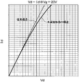
- FIG. 3 shows Vd ⁇ Id which is a characteristic of the drain current Id with respect to the drain voltage Vd for the structure of the present embodiment provided with the high concentration n-type layer 20 and the conventional structure not provided with the high concentration n-type layer 20.
- the result of comparing the characteristics is shown. The characteristics are shown when the gate voltage is 20 V and the drain voltage is changed.
- the drain current Id when the drain voltage Vd is high that is, the saturation current value is large.
- the saturation current value is not so large, and has been reduced to, for example, about 1/5 of the conventional structure.
- the drain current Id can be reduced even when the drain voltage Vd becomes high. For this reason, a low saturation current can be realized.
- FIG. 4 shows a result of comparing the Vd-Id characteristics in the range of the drain voltage Vd assumed to be the normal operation range of the SiC semiconductor device, that is, the normal operation in FIG. The figure which expanded the range is shown.
- the structure of the present embodiment also has substantially the same characteristics as the conventional structure. Specifically, at the same drain voltage Vd, the drain current Id was slightly larger in the conventional structure than in the structure of the present embodiment, but almost the same value. From this, it can be seen that the on-resistance equivalent to that of the conventional structure can be achieved in the structure of the present embodiment.
- the high-concentration n-type layer 20 is also formed on the upper surface of the n ⁇ -type drift layer 2 below the p-type deep layer 3. For this reason, the extension amount of the depletion layer extending from the p-type deep layer 3 to the n ⁇ -type drift layer 2 side is also suppressed, and the on-resistance can be further reduced.
- n-type impurity concentrations and thicknesses such as the JFET portion 2a and the high-concentration n-type layer 20 are shown, these are only examples.
- the n-type impurity concentration and thickness are set so as to satisfy a desired pinch-off condition.
- the JFET portion 2a is designed as a condition for pinching off at 10% of the breakdown voltage of the semiconductor element, for example. That is, the n-type impurity concentration Nd1 and the thickness W1 are designed so that the following formula 1 is satisfied, where the n-type impurity concentration of the JFET portion 2a is Nd1, the thickness is W1, the pinch-off voltage is Vp1, the elementary charge is q1, and the dielectric constant is ⁇ 1. is doing.
- the high concentration n-type layer 20 is designed, for example, as a condition that does not pinch off at 0.1% of the breakdown voltage of the semiconductor element. That is, assuming that the n-type impurity concentration of the high-concentration n-type layer 20 is Nd2, the thickness on the side surface of the p-type deep layer 3 is W2, the pinch-off voltage is Vp2, the elementary charge is q2, the dielectric constant is ⁇ 2, and The n-type impurity concentration Nd2 and the thickness W2 are designed so as to satisfy.
- Vp2 (q2 ⁇ Nd2 ⁇ W2 2 ) / 2 ⁇ 2> 0.1% of the breakdown voltage of the semiconductor element
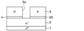
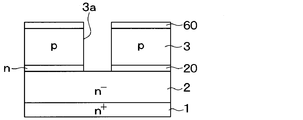
- n + type substrate 1 is prepared as a semiconductor substrate. After forming n ⁇ type drift layer 2 made of SiC on the main surface of n + type substrate 1 by epitaxial growth, a part of high-concentration n type layer 20 made of SiC is formed on n ⁇ type drift layer 2. And a p-type deep layer 3 made of SiC is formed.
- a mask (not shown) having an opening corresponding to the JFET portion 2a is formed on the p-type deep layer 3, and the p-type deep layer 3 is removed using the mask to form a trench 3a.
- the bottom of the trench 3a N ⁇ type drift layer 2 is exposed.
- High-concentration n-type layer 20 and JFET portion 2a are formed by performing buried epitaxial growth while the surface of p-type deep layer 3 other than trench 3a is covered with a mask.
- the n-type layer is formed with a concentration difference, and is formed at a high concentration at the initial stage of growth and at a low concentration thereafter.
- the high-concentration n-type layer 20 is first formed on the side surface of the trench 3a, and the JFET portion 2a is formed so as to fill the trench 3a. Thereafter, a mask (not shown) is removed. Further, as necessary, the surfaces of the p-type deep layer 3, the high-concentration n-type layer 20, and the JFET portion 2a are planarized.
- n-type current distribution layer 4 is epitaxially grown on the surfaces of the p-type deep layer 3, the high-concentration n-type layer 20, and the JFET portion 2a.
- a p-type coupling layer 5 is formed by ion-implanting and activating p-type impurities at a position away from the JFET portion 2a and the high-concentration n-type layer 20 in the n-type current spreading layer 4.
- a p-type base region 6 and an n + -type source region 7 are epitaxially grown on the n-type current spreading layer 4 and the p-type coupling layer 5.
- a p + type contact region 8 is formed by ion implantation of a p type impurity into a part of the n + type source region 7.
- Step shown in FIG. 5H After forming a mask (not shown) on the n + -type source region 7 and the like, a region where the gate trench 9 is to be formed in the mask is opened. Then, by performing anisotropic etching such as RIE (Reactive Ion Etching) using a mask, the gate trench 9 is formed.
- anisotropic etching such as RIE (Reactive Ion Etching)
- the gate insulating film 10 covers the inner wall surface of the gate trench 9 and the surface of the n + -type source region 7. Then, after depositing Poly-Si doped with p-type impurities or n-type impurities, this is etched back to leave the Poly-Si at least in the gate trench 9 to form the gate electrode 11.
- An interlayer insulating film 12 made of, for example, an oxide film is formed so as to cover the surfaces of the gate electrode 11 and the gate insulating film 10. Further, after forming a mask (not shown) on the surface of the interlayer insulating film 12, a portion of the mask located between the gate electrodes 11, that is, a portion corresponding to the p + type contact region 8 and its vicinity are opened. Thereafter, the interlayer insulating film 12 is patterned using a mask to form a contact hole exposing the p-type deep layer 3 and the n + -type source region 7. And after forming the electrode material comprised by the laminated structure of a some metal, for example on the surface of the interlayer insulation film 12, the source electrode 13 is formed by patterning an electrode material.
- a drain electrode 14 is formed on the back side of the n + type substrate 1. Thereby, the SiC semiconductor device according to the present embodiment is completed.
- the high-concentration n-type layer 20 is formed at least on the side surface of the p-type deep layer 3, that is, between the p-type deep layer 3 and the JFET portion 2a. Yes.
- the high-concentration n-type layer 20 functions as a layer that stops the extension of the depletion layer, and it is possible to suppress the extension of the depletion layer into the JFET portion 2a. Since the narrowing can be suppressed, a low on-resistance can be achieved. Further, when the drain voltage Vd becomes higher than the voltage during normal operation due to a load short circuit or the like, the depletion layer extending from the p-type deep layer 3 side to the high-concentration n-type layer 20 extends beyond the thickness of the high-concentration n-type layer 20. The JFET portion 2a is immediately pinched off.
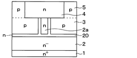
- the vertical MOSFET has a structure in which the JFET portion 2a is located immediately below the trench gate structure because the current path can be minimized.
- the JFET portion 2a is located at a position shifted from directly below the trench gate structure as shown in FIG. 6 due to misalignment of the mask, the above effect can be obtained.
- a low concentration p-type layer 30 is provided instead of the high concentration n-type layer 20 provided in the SiC semiconductor device of the first embodiment.
- the low concentration p-type layer 30 functions as a depletion layer adjustment layer.
- the low concentration p-type layer 30 is formed at least on the side surface of the p-type deep layer 3, that is, between the p-type deep layer 3 and the JFET portion 2a.
- a low-concentration p-type layer 30 is also formed at the position.
- the low-concentration p-type layer 30 has an impurity concentration lower than that of the JFET portion 2a and the p-type deep layer 3, for example, the p-type impurity concentration is 1.0 ⁇ 10 17 / cm 3 .
- the thickness of the low-concentration p-type layer 30 is 0.05 ⁇ m on the side surface of the p-type deep layer 3 and 0.07 ⁇ m on the upper surface of the n ⁇ -type drift layer 2.
- the p-type impurity concentration of the low-concentration p-type layer 30 and the thickness on the side surface of the p-type deep layer 3 are designed to satisfy a desired pinch-off condition.
- the low-concentration p-type layer 30 is designed, for example, as a condition that does not pinch off at 0.1% of the breakdown voltage of the semiconductor element. That is, assuming that the p-type impurity concentration of the low-concentration p-type layer 30 is Na, the thickness on the side surface of the p-type deep layer 3 is W3, the pinch-off voltage is Vp3, the elementary charge is q3, and the dielectric constant is ⁇ 3, The n-type impurity concentration Nd3 and the thickness W3 are designed so as to satisfy.
- Vp3 (q3 ⁇ Na ⁇ W3 2 ) / 2 ⁇ 3> 0.1% of the breakdown voltage of the semiconductor element
- the impurity concentration of the JFET portion 2a is changed, and the n-type impurity concentration is 1.0 ⁇ 10 17 / cm 3 .
- the n-type impurity concentration of the JFET portion 2a described here is designed to satisfy Equation 2 described in the first embodiment together with the thickness of the JFET portion 2a.
- the impurity concentration difference between the JFET portion 2a and the low-concentration p-type layer 30 is different from that of the JFET portion 2a and the p-type layer 30.
- This is smaller than the impurity concentration difference with the deep layer 3.
- the extension amount of the depletion layer extending from the low concentration p-type layer 30 to the JFET portion 2a side is suppressed. Therefore, it is possible to suppress the current path in the JFET portion 2a from being narrowed by the depletion layer, and to achieve a low on-resistance. Therefore, even with the configuration of the present embodiment, it is possible to obtain the same effect as that of the first embodiment.
- the manufacturing method of the SiC semiconductor device of the present embodiment is almost the same as that of the first embodiment. That is, when the high concentration n-type layer 20 described in the first embodiment is formed, the same steps as in the first embodiment are performed except that the low concentration p-type layer 30 is formed instead. SiC semiconductor devices can be manufactured.
- the high-concentration n-type layer 20 described in the first embodiment and the low-concentration p-type layer 30 described in the second embodiment can be combined.
- a high-concentration n-type layer 20 is provided on the upper surface of the n ⁇ -type drift layer 2
- a low-concentration p-type layer 30 is provided on the side surface of the p-type deep layer 3.
- a low concentration p-type layer 30 is provided on the upper surface of the n ⁇ -type drift layer 2
- a high concentration n-type layer 20 is provided on the side surface of the p-type deep layer 3.
- a third embodiment will be described.
- a super junction structure is applied to the first and second embodiments, and the other aspects are the same as those in the first and second embodiments. Therefore, the present embodiment is different from the first and second embodiments. Only the part will be described.
- the case where the super junction structure is applied to the vertical MOSFET having the high-concentration n-type layer 20 as in the first embodiment will be described, but the low-concentration p-type layer 30 as in the second embodiment is described.
- the present invention is also applicable to a vertical MOSFET having the high-concentration n-type layer 20 as in the first embodiment.
- a p-type column layer 40 extending toward the n ⁇ -type drift layer 2 is provided below the p-type deep layer 3.
- the p-type column layer 40 has a structure in contact with the n + -type substrate 1, may have a structure in which apart from the n + -type substrate 1.
- a PN junction super junction structure having the n ⁇ -type drift layer 2 as the n-type column layer is formed.
- the high-concentration n-type layer 20 is also formed for the vertical MOSFET having such a super junction structure. For this reason, the effect similar to 1st Embodiment can be acquired.
- the SiC semiconductor device having the structure of this embodiment can also be basically manufactured by the same manufacturing method as that of the first embodiment.
- the p-type column layer 40 can be formed by forming a trench in the n ⁇ -type drift layer 2, performing buried epitaxial growth, and further etching back to planarize the surface of the p-type column layer 40. Except for this, the SiC semiconductor device of this embodiment can be manufactured by the same method as in the first embodiment.
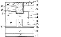
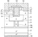
- FIG. 13 A fourth embodiment will be described.
- the contact structure of the source electrode 13 is changed with respect to the first to third embodiments, and the rest is the same as the first to third embodiments. Only the parts different from the form will be described.
- a case will be described in which the contact structure of the source electrode 13 is changed with respect to the vertical MOSFET having the high-concentration n-type layer 20 as in the first embodiment, but the low-concentration p as in the second embodiment is described.
- the present invention can also be applied to a vertical MOSFET having a mold layer 30.
- a contact trench 50 is formed on the opposite side of the trench gate structure with the n + type source region 7 interposed therebetween.
- a p + type contact region 8 is formed in the surface layer portion of the p type base region 6 on the bottom surface of the contact trench 50.
- Such a structure can be realized by forming the contact trench 50 by etching after forming the n + -type source region 7 and then performing ion implantation for forming the p + -type contact region 8.
- contact between the source electrode 13 and the p-type base region 6 may be achieved by removing a part of the n + -type source region 7 by the contact trench 50.
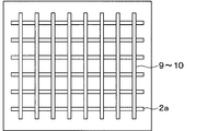
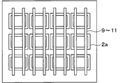
- FIG. 1 A fifth embodiment will be described.
- the top surface layout of the JFET portion 2a is changed with respect to the first to fourth embodiments, and the other aspects are the same as those of the first to fourth embodiments. Only the parts different from the form will be described.
- the case where the layout configuration is changed for the vertical MOSFET having the high-concentration n-type layer 20 as in the first embodiment will be described, but the low-concentration p-type layer 30 as in the second embodiment is used.
- the present invention can also be applied to a vertical MOSFET having the same.
- the JFET portion 2a is formed in a strip shape along the longitudinal direction of the trench gate structure.
- the JFET portion 2a is laid out so as to intersect, in this case, perpendicular to the longitudinal direction of the trench gate structure, so that the trench gate structure and the JFET portion 2a are laid out. Are arranged in a grid pattern.
- the trench gate structure and the JFET portion 2a are not limited to the lattice layout, but may be other layouts.
- the JFET portion 2a may be formed in a frame shape such as a quadrangle, and the JFET portions 2a may be arranged in a lattice shape.
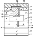
- FIG. 10 A sixth embodiment will be described.
- the present embodiment is different from the first to fifth embodiments in that a planar type vertical MOSFET is used instead of the trench gate type vertical MOSFET, and the rest is the same as in the first to fifth embodiments. Therefore, only the parts different from the first to fifth embodiments will be described.
- a case where a planar structure is used for the vertical MOSFET having the high-concentration n-type layer 20 as in the first embodiment will be described, but the low-concentration p-type layer 30 as in the second embodiment is provided.
- the present invention can also be applied to a vertical MOSFET.
- a structure including the high-concentration n-type layer 20 can also be applied to an SiC semiconductor device having a planar type vertical MOSFET as shown in FIG.
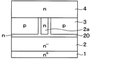
- a planar structure a p-type base region 6 is formed on the n ⁇ -type drift layer 2, and an n + -type source region 7 is formed on the surface layer portion of the p-type base region 6.
- a JFET portion 2 a is formed so as to be sandwiched between the p-type base regions 6.
- the surface side of the portion of the p-type base region 6 located between the n + -type source region 7 and the JFET portion 2a is defined as a channel region, and the gate electrode 11 is formed on the channel region via the gate insulating film 10. The structure is formed.
- the same effect as that of the first embodiment can be obtained by providing the high-concentration n-type layer 20 at least on the side surface of the p-type base region 6.
- the high-concentration n-type layer 20 is also formed on the upper surface of the n ⁇ -type drift layer 2. For this reason, the amount of extension of the depletion layer extending from the p-type base region 6 to the n ⁇ -type drift layer 2 side is also suppressed, and the on-resistance can be further reduced.
- a seventh embodiment will be described.
- the method for forming the high-concentration n-type layer 20 and the low-concentration p-type layer 30 is changed with respect to the first to sixth embodiments. Therefore, only the differences from the first to sixth embodiments will be described.
- the case where the manufacturing method of this embodiment is applied to the vertical MOSFET having the high-concentration n-type layer 20 as in the first embodiment will be described, but the low-concentration p as in the second embodiment is described.
- the present invention can also be applied to a vertical MOSFET having a mold layer 30.
- the high concentration n-type layer 20 is formed by another method.
- the p-type deep layer 3 is epitaxially grown.
- an n-type layer 60 is formed on the p-type deep layer 3.
- the n-type layer 60 may be formed by epitaxial growth, but here it is formed by ion implantation of n-type impurities. Further, the impurity concentration of the n-type layer 60 is set to be approximately the same as that of the high-concentration n-type layer 20. Thereafter, as shown in FIG.
- a trench 3 a is formed so as to penetrate the n-type layer 60 in addition to the p-type deep layer 3.
- the trench 3a corresponds to a first trench.
- annealing is performed, for example, heating is performed in a mixed gas atmosphere of hydrogen (H 2) and argon (Ar) serving as an etching gas.
- H 2 hydrogen
- Ar argon
- the SiC semiconductor device including the vertical MOSFET having the same structure as that shown in FIG. 1 can be manufactured by performing the steps described in the first embodiment.
- the n-type layer 60 is formed on the p-type deep layer 3, and the n-type layer 60 is melted and fluidized by an annealing process, so that a high concentration n is formed on the side surface of the p-type deep layer 3 or the like.
- the mold layer 20 may be formed.
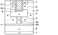
- FIG. 16A the steps shown in FIGS. 5A to 5D described in the first embodiment are performed.
- FIG. 16B the p-type base region 6 and the n + -type source region 7 are formed on the n-type current spreading layer 4 without forming the p-type coupling layer 5, and the trench gate structure is further formed.
- FIG. 16C the trench that reaches the p-type deep layer 3 through the n + -type source region 7, the p-type base region 6, and the n-type current distribution layer 4 at a position away from the trench gate structure. 70 is formed.
- This trench 70 corresponds to a second trench.
- a p-type layer 71 that functions as the p-type coupling layer 5 and the p + -type contact region 8 is formed by buried epitaxial growth.
- the p-type layer 71 that functions as the p-type coupling layer 5 and the p + -type contact region 8 may be formed by epitaxial growth.
- the p-type deep layer 3 is connected to the source electrode 13 to obtain the source potential.
- the p-type deep layer 3 is separated from the p-type base region 6, and the second gate for adjusting the extension amount of the depletion layer of the JFET portion 2 a in accordance with the voltage application to the p-type deep layer 3. You may make it function.
- the p-type deep layer 3 can be configured to be electrically connected to the gate electrode 11 and applied with a gate voltage, or connected to the drain electrode 14 and applied to the drain voltage.
- the width of the JFET portion 2a does not need to be constant, and for example, the JFET portion 2a may have a tapered cross section so that the width gradually decreases toward the drain electrode 14 side.
- the impurity concentration in each part may not be constant.
- a structure having an impurity concentration gradient in which the p-type impurity concentration decreases as the p-type deep layer 3 approaches the drain electrode 14 and increases as the p-type deep layer 3 approaches the source electrode 13 may be employed.
- the dimensions and impurity concentrations of the respective parts constituting the SiC semiconductor device described in the above embodiments are merely examples.
- the dimensions and impurity concentration of each part may be appropriately set based on the pinch-off conditions of the high-concentration n-type layer 20, the low-concentration p-type layer 30, and the JFET portion 2a.
- the width of the high concentration n-type layer 20 can be increased.
- the n-type impurity concentration is 3.0 ⁇ 10 17 / cm 3
- the width of the JFET portion 2 a is 0.4 ⁇ m and 1.0 ⁇ 10 6. 18 / cm 3 .
- the half cell pitch can be increased, for example, 3 ⁇ m.
- the n-type current distribution layer 4 and the p-type coupling layer 5 can be made thin to increase the impurity concentration.
- the thickness is set to 0.4 ⁇ m, and the n-type impurity concentration and the p-type impurity concentration are set to 6 ⁇ m, respectively. It can also be set to 0.0 ⁇ 10 17 / cm 3 . Further, the thickness of the p-type deep layer 3 can be reduced to increase the impurity concentration. For example, the thickness can be 0.6 ⁇ m, and the p-type impurity concentration can be 2.0 ⁇ 10 18 / cm 3 . In addition, the same dimensions and the same impurity concentration as the example shown here can be applied to the structure including the low-concentration p-type layer 30. However, those listed here are only examples, and other dimensions and impurity concentrations may be used.
- an n-channel type vertical MOSFET in which the first conductivity type is n-type and the second conductivity type is p-type has been described as an example.
- An inverted p-channel type vertical MOSFET may be used.
- the vertical MOSFET has been described as an example of the semiconductor element.
- the present disclosure can be applied to an IGBT having a similar structure. The IGBT only changes the conductivity type of the n + type substrate 1 from the n-type to the p-type with respect to the above-described embodiments, and the other structures and manufacturing methods are the same as those in the above-described embodiments.
- the SiC semiconductor device is described as an example of the semiconductor device.
- the present disclosure can be applied to a semiconductor device using Si, and other wide band gap semiconductor devices such as GaN and diamond.
- the above embodiments can also be applied to semiconductor devices using AlN or the like.
Landscapes
- Junction Field-Effect Transistors (AREA)
Applications Claiming Priority (2)
| Application Number | Priority Date | Filing Date | Title |
|---|---|---|---|
| JP2016184257A JP6683083B2 (ja) | 2016-09-21 | 2016-09-21 | 半導体装置およびその製造方法 |
| JP2016-184257 | 2016-09-21 |
Publications (1)
| Publication Number | Publication Date |
|---|---|
| WO2018056357A1 true WO2018056357A1 (ja) | 2018-03-29 |
Family
ID=61689519
Family Applications (1)
| Application Number | Title | Priority Date | Filing Date |
|---|---|---|---|
| PCT/JP2017/034101 Ceased WO2018056357A1 (ja) | 2016-09-21 | 2017-09-21 | 半導体装置およびその製造方法 |
Country Status (2)
| Country | Link |
|---|---|
| JP (1) | JP6683083B2 (enExample) |
| WO (1) | WO2018056357A1 (enExample) |
Cited By (5)
| Publication number | Priority date | Publication date | Assignee | Title |
|---|---|---|---|---|
| CN110190128A (zh) * | 2019-05-29 | 2019-08-30 | 西安电子科技大学芜湖研究院 | 一种碳化硅双侧深l形基区结构的mosfet器件及其制备方法 |
| CN111463277A (zh) * | 2019-01-21 | 2020-07-28 | 株式会社电装 | 半导体器件 |
| CN113767478A (zh) * | 2019-04-23 | 2021-12-07 | 株式会社电装 | 半导体装置及其制造方法 |
| US11201239B2 (en) | 2017-09-18 | 2021-12-14 | Denso Corporation | Semiconductor device including saturation current suppression layer |
| CN116504808A (zh) * | 2023-04-18 | 2023-07-28 | 湖北九峰山实验室 | 宽禁带半导体包角沟槽mosfet器件结构及其制作方法 |
Families Citing this family (3)
| Publication number | Priority date | Publication date | Assignee | Title |
|---|---|---|---|---|
| JP7327905B2 (ja) | 2017-07-07 | 2023-08-16 | 株式会社デンソー | 半導体装置およびその製造方法 |
| JP7167717B2 (ja) * | 2019-01-07 | 2022-11-09 | 株式会社デンソー | 半導体装置 |
| JP7319501B2 (ja) | 2019-10-09 | 2023-08-02 | 株式会社東芝 | 基板の製造方法、半導体装置の製造方法、基板及び半導体装置 |
Citations (7)
| Publication number | Priority date | Publication date | Assignee | Title |
|---|---|---|---|---|
| JP2007096139A (ja) * | 2005-09-29 | 2007-04-12 | Denso Corp | 半導体基板の製造方法 |
| JP2012033731A (ja) * | 2010-07-30 | 2012-02-16 | Mitsubishi Electric Corp | 電力用半導体素子 |
| JP2013179221A (ja) * | 2012-02-29 | 2013-09-09 | Toshiba Corp | 半導体装置及びその製造方法 |
| WO2013187017A1 (ja) * | 2012-06-13 | 2013-12-19 | 株式会社デンソー | 炭化珪素半導体装置およびその製造方法 |
| WO2015104949A1 (ja) * | 2014-01-10 | 2015-07-16 | 三菱電機株式会社 | 炭化珪素半導体装置および炭化珪素半導体装置の製造方法 |
| JP2015141921A (ja) * | 2014-01-27 | 2015-08-03 | トヨタ自動車株式会社 | 半導体装置 |
| JP2016058660A (ja) * | 2014-09-11 | 2016-04-21 | 富士電機株式会社 | 半導体装置 |
-
2016
- 2016-09-21 JP JP2016184257A patent/JP6683083B2/ja active Active
-
2017
- 2017-09-21 WO PCT/JP2017/034101 patent/WO2018056357A1/ja not_active Ceased
Patent Citations (7)
| Publication number | Priority date | Publication date | Assignee | Title |
|---|---|---|---|---|
| JP2007096139A (ja) * | 2005-09-29 | 2007-04-12 | Denso Corp | 半導体基板の製造方法 |
| JP2012033731A (ja) * | 2010-07-30 | 2012-02-16 | Mitsubishi Electric Corp | 電力用半導体素子 |
| JP2013179221A (ja) * | 2012-02-29 | 2013-09-09 | Toshiba Corp | 半導体装置及びその製造方法 |
| WO2013187017A1 (ja) * | 2012-06-13 | 2013-12-19 | 株式会社デンソー | 炭化珪素半導体装置およびその製造方法 |
| WO2015104949A1 (ja) * | 2014-01-10 | 2015-07-16 | 三菱電機株式会社 | 炭化珪素半導体装置および炭化珪素半導体装置の製造方法 |
| JP2015141921A (ja) * | 2014-01-27 | 2015-08-03 | トヨタ自動車株式会社 | 半導体装置 |
| JP2016058660A (ja) * | 2014-09-11 | 2016-04-21 | 富士電機株式会社 | 半導体装置 |
Cited By (10)
| Publication number | Priority date | Publication date | Assignee | Title |
|---|---|---|---|---|
| US11201239B2 (en) | 2017-09-18 | 2021-12-14 | Denso Corporation | Semiconductor device including saturation current suppression layer |
| US11637198B2 (en) | 2017-09-18 | 2023-04-25 | Denso Corporation | Manufacturing method of semiconductor device including semiconductor element of inversion type |
| CN111463277A (zh) * | 2019-01-21 | 2020-07-28 | 株式会社电装 | 半导体器件 |
| CN111463277B (zh) * | 2019-01-21 | 2023-12-19 | 株式会社电装 | 半导体器件 |
| CN113767478A (zh) * | 2019-04-23 | 2021-12-07 | 株式会社电装 | 半导体装置及其制造方法 |
| CN113767478B (zh) * | 2019-04-23 | 2023-12-05 | 株式会社电装 | 半导体装置及其制造方法 |
| CN110190128A (zh) * | 2019-05-29 | 2019-08-30 | 西安电子科技大学芜湖研究院 | 一种碳化硅双侧深l形基区结构的mosfet器件及其制备方法 |
| CN110190128B (zh) * | 2019-05-29 | 2024-03-19 | 西安电子科技大学芜湖研究院 | 一种碳化硅双侧深l形基区结构的mosfet器件及其制备方法 |
| CN116504808A (zh) * | 2023-04-18 | 2023-07-28 | 湖北九峰山实验室 | 宽禁带半导体包角沟槽mosfet器件结构及其制作方法 |
| CN116504808B (zh) * | 2023-04-18 | 2025-09-26 | 湖北九峰山实验室 | 宽禁带半导体包角沟槽mosfet器件结构及其制作方法 |
Also Published As
| Publication number | Publication date |
|---|---|
| JP6683083B2 (ja) | 2020-04-15 |
| JP2018049928A (ja) | 2018-03-29 |
Similar Documents
| Publication | Publication Date | Title |
|---|---|---|
| US11476360B2 (en) | Semiconductor device and method for manufacturing the same | |
| US11107911B2 (en) | Semiconductor device and method for manufacturing same | |
| JP5728992B2 (ja) | 炭化珪素半導体装置およびその製造方法 | |
| JP6683083B2 (ja) | 半導体装置およびその製造方法 | |
| CN110050349B (zh) | 碳化硅半导体装置及其制造方法 | |
| JP2012169385A (ja) | 炭化珪素半導体装置 | |
| US11637198B2 (en) | Manufacturing method of semiconductor device including semiconductor element of inversion type | |
| JP2012169384A (ja) | 炭化珪素半導体装置およびその製造方法 | |
| CN105593996A (zh) | 碳化硅半导体装置 | |
| WO2019009091A1 (ja) | 半導体装置およびその製造方法 | |
| JP2018056463A (ja) | 半導体装置及びその製造方法 | |
| JP5556863B2 (ja) | ワイドバンドギャップ半導体縦型mosfet | |
| JP7095342B2 (ja) | 炭化珪素半導体装置およびその製造方法 | |
| JP2023070568A (ja) | 半導体装置およびその製造方法 | |
| JP7206919B2 (ja) | 半導体装置 | |
| JP2019165164A (ja) | 炭化珪素半導体装置およびその製造方法 | |
| CN101233618B (zh) | 半导体装置及其制造方法 | |
| JP7127315B2 (ja) | 炭化珪素半導体装置およびその製造方法 | |
| WO2019181962A1 (ja) | 半導体装置およびその製造方法 | |
| JP7167717B2 (ja) | 半導体装置 | |
| JP7619168B2 (ja) | 半導体装置 | |
| KR102251761B1 (ko) | 전력 반도체 소자 | |
| JP2006080185A (ja) | 半導体装置の製造方法 | |
| JP5389339B2 (ja) | 半導体装置 |
Legal Events
| Date | Code | Title | Description |
|---|---|---|---|
| 121 | Ep: the epo has been informed by wipo that ep was designated in this application |
Ref document number: 17853126 Country of ref document: EP Kind code of ref document: A1 |
|
| NENP | Non-entry into the national phase |
Ref country code: DE |
|
| 122 | Ep: pct application non-entry in european phase |
Ref document number: 17853126 Country of ref document: EP Kind code of ref document: A1 |