WO2018043377A1 - 磁気トンネル接合素子を備える磁気メモリの製造方法 - Google Patents
磁気トンネル接合素子を備える磁気メモリの製造方法 Download PDFInfo
- Publication number
- WO2018043377A1 WO2018043377A1 PCT/JP2017/030682 JP2017030682W WO2018043377A1 WO 2018043377 A1 WO2018043377 A1 WO 2018043377A1 JP 2017030682 W JP2017030682 W JP 2017030682W WO 2018043377 A1 WO2018043377 A1 WO 2018043377A1
- Authority
- WO
- WIPO (PCT)
- Prior art keywords
- magnetic
- substrate
- tunnel junction
- annealing
- magnetic field
- Prior art date
- Legal status (The legal status is an assumption and is not a legal conclusion. Google has not performed a legal analysis and makes no representation as to the accuracy of the status listed.)
- Ceased
Links
Images






Classifications
-
- H—ELECTRICITY
- H10—SEMICONDUCTOR DEVICES; ELECTRIC SOLID-STATE DEVICES NOT OTHERWISE PROVIDED FOR
- H10N—ELECTRIC SOLID-STATE DEVICES NOT OTHERWISE PROVIDED FOR
- H10N50/00—Galvanomagnetic devices
- H10N50/01—Manufacture or treatment
-
- H—ELECTRICITY
- H10—SEMICONDUCTOR DEVICES; ELECTRIC SOLID-STATE DEVICES NOT OTHERWISE PROVIDED FOR
- H10B—ELECTRONIC MEMORY DEVICES
- H10B61/00—Magnetic memory devices, e.g. magnetoresistive RAM [MRAM] devices
- H10B61/20—Magnetic memory devices, e.g. magnetoresistive RAM [MRAM] devices comprising components having three or more electrodes, e.g. transistors
- H10B61/22—Magnetic memory devices, e.g. magnetoresistive RAM [MRAM] devices comprising components having three or more electrodes, e.g. transistors of the field-effect transistor [FET] type
Definitions
- the present invention relates to a method for manufacturing a magnetic memory including a magnetic tunnel junction element.
- a nonvolatile memory such as an MRAM using a magnetoresistive effect element is known (see, for example, Patent Document 1).
- a magnetoresistive effect element for example, as shown in FIG. 16, a magnetic tunnel junction element (MTJ element) in which a barrier layer 112 (nonmagnetic barrier layer) is disposed between a reference layer 111 as a magnetic layer and a recording layer 113 is used.
- the reference layer 111 whose magnetization direction is difficult to change is magnetized in a direction perpendicular to the layer surface (film surface).
- the recording layer 113 has a variable magnetization direction.
- the saturation magnetization M s of the recording layer 113 is defined by the material, structure, temperature, etc. of the recording layer 113.
- the magnetoresistive effect element shown in FIG. 16 is referred to as a so-called perpendicular magnetization MTJ element.
- the MTJ element has a structure in which information can be recorded by making two resistance states correspond to bit information “0” and “1”, respectively.
- the energy E b of the recording layer 113 is the angle ⁇ between the magnetization direction of the recording layer 113 and the magnetization direction of the reference layer 111, and the magnetic difference of the reference layer 111.
- Equation (1) the isotropic energy density K eff and the volume V of the recording layer 113, it is expressed by Equation (1).
- Equation (1) an energy barrier (E b ) required for magnetization reversal is obtained.
- a non-volatile memory such as an MRAM having a magnetoresistive effect element (MTJ element) has a thermal stability index as an indicator of the stability of bit information.
- This thermal stability index ⁇ 0 is expressed by Equation (2) using the Boltzmann constant k B and the absolute temperature T.
- the probability P that the recording layer having the thermal stability index ⁇ 0 undergoes magnetization reversal after time t is expressed by Equation (3) according to the Neel-Arrhenius law (for example, see Non-Patent Document 1). As shown in FIG. 17B, the time t when the probability P is 50% corresponds to the information holding time by the recording layer 113.
- a magnetic field pulse method As a general method for measuring the thermal stability index ⁇ 0 , a magnetic field pulse method, a current pulse method, and the like are known.
- the magnetization reversal probability when a magnetic field pulse having a specific pulse width is applied is measured while changing the magnetic field magnitude of the magnetic field pulse, and the thermal reversal probability is determined based on the relationship between the magnetic field magnitude and the magnetization reversal probability.
- the stability index ⁇ 0 is obtained.
- the magnetization reversal probability when a current pulse with a specific pulse width is applied is measured while changing the current magnitude of the current pulse, and based on the relationship between the current magnitude and the magnetization reversal probability,
- the sex index ⁇ 0 is obtained.
- an MRAM chip composed of an MTJ of 10 Mb or more is prepared, and information of 1 or 0 is recorded on the recording layer of each MTJ by a checkerboard pattern or the like. After standing at high temperature for several minutes to 100 hours, measure the error rate indicating how much initial information was lost, and based on the relationship between the inversion probability calculated from the error rate and the standing time A method for obtaining the thermal stability index ⁇ 0 is known. According to this method, since the value of the energy barrier does not change during the measurement, an accurate thermal stability index ⁇ 0 can be obtained regardless of the magnetization reversal mode.
- a manufacturing method of a magnetic memory using a magnetoresistive effect element for example, a CMOS is manufactured on a wafer serving as a substrate, an intermediate wiring for connecting to an MTJ is formed on the CMOS, and a magnetic material is formed above the intermediate wiring.
- MTJ patterns are produced, MTJ is formed by etching, a protective film is formed, upper wiring is formed on the MTJ, and this is formed into a chip shape
- a method is known in which resin sealing is performed after cutting into a predetermined circuit board using a wire bonding metal wire.
- Patent Document 2 a magnetic detection element assembled in a bridge shape is formed on a substrate, and a protective film for protecting the magnetic detection element is formed on the substrate, whereby the substrate is a multilayer substrate, and the protective film
- a stress relieving groove is formed by etching the protective film in the vicinity of the magnetic sensing element in the step, and the multilayer substrate is packaged after the stress relieving groove is formed.
- a method of manufacturing a magnetic sensor is described in which the multilayer substrate is annealed prior to packaging the substrate.
- the magnetic sensor manufacturing method described in Patent Document 2 requires a complicated process of forming stress relaxation grooves. As described in Patent Document 2, when annealing is performed before the package, the stress remaining after the package cannot be removed.
- a method of manufacturing a magnetic memory including a magnetic tunnel junction element (magnetoresistance effect element) includes at least the following configuration.
- a method of manufacturing a magnetic memory comprising a magnetic tunnel junction element (magnetoresistance effect element), Forming a magnetic film having a nonmagnetic layer between the first magnetic layer and the second magnetic layer on a substrate provided with an electrode layer;
- a protective film forming step of forming a protective film for protecting the magnetic tunnel junction element formed on the substrate After the protective film forming step, forming a component of a magnetic memory on the substrate on which the protective film is formed, a forming step with a thermal history, A magnetic field non-
- the method for manufacturing a magnetic memory using the magnetic tunnel junction element according to the present invention can easily manufacture a magnetic memory including a magnetic tunnel junction element having high element performance (such as a thermal stability index).
- FIG. 1A and 1B are views for explaining a magnetic memory (semiconductor integrated circuit) using a magnetic tunnel junction device according to an embodiment of the present invention
- FIG. 1A is a perspective view showing an example of a magnetic memory (semiconductor integrated circuit)
- the conceptual diagram which shows an example of the manufacturing apparatus of the magnetic memory (semiconductor integrated circuit) which concerns on embodiment of this invention.
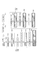
- 6 is a flowchart showing an example of a method for manufacturing a magnetic memory using the magnetic tunnel junction element according to the embodiment of the present invention.
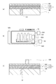
- the figure which shows an example of the manufacturing method of a magnetic memory (a) is a figure for demonstrating a magnetic film formation process, (b) is a figure for demonstrating annealing treatment in a magnetic field (heat processing in a magnetic field), (c) is The figure for demonstrating the process of forming the resist pattern for MTJ patterning.
- the conceptual diagram for demonstrating an example of the manufacturing method of a magnetic memory (a) is a figure for demonstrating the patterning of MTJ, (b) is a figure for demonstrating the formation process of a capture film
- C) is a figure for demonstrating lower electrode formation (patterning).
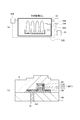
- a conceptual diagram for explaining an example of a manufacturing method of a magnetic memory (a) is a diagram for explaining a heat treatment (annealing process) using a heat treatment apparatus (annealing apparatus), and (b) is a second interlayer film formed. The figure for demonstrating the process to do.
- the conceptual diagram for demonstrating an example of the manufacturing method of a magnetic memory (a) is a figure for demonstrating the process of planarizing a 2nd interlayer film, (b) is heat processing using a heat processing apparatus (annealing apparatus) ( The figure for demonstrating annealing treatment.
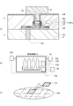
- the conceptual diagram for demonstrating an example of the manufacturing method of a magnetic memory (a) is sectional drawing which shows an example of the state which formed the via in the 2nd interlayer film, (b) is an example of the state in which the diffusion prevention film was formed The figure for demonstrating, (c) is a figure for demonstrating an example of the state which formed the upper wiring.
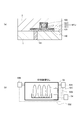
- a conceptual diagram for explaining an example of a manufacturing method of a magnetic memory (a) is a diagram for explaining patterning of an upper wiring, and (b) is a heat treatment (annealing process) using a heat treatment apparatus (annealing apparatus).
- C The figure for demonstrating the process of cutting out a chip
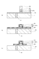
- the figure which shows an example of the manufacturing method of a magnetic memory (a) is sectional drawing which shows an example of the state which carried out die bonding of the chip
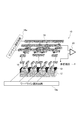
- the perspective view which shows an example of the MTJ array structure of the magnetic memory (semiconductor integrated circuit) using the magnetic tunnel junction element concerning embodiment of this invention.
- FIG. 14 is a diagram showing an example of a thermal stability index of an MTJ element manufactured by the magnetic memory manufacturing method shown in FIG. 13 and an MTJ element of a comparative example.
- the conceptual diagram which shows an example of the measurement system which measures the thermal stability index
- the schematic diagram for demonstrating the MTJ element provided with a reference layer, a barrier layer, and a recording layer.
- FIG. 4A is a diagram for explaining a recording layer of an MTJ element
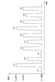
- FIG. 3A is a diagram showing a relationship between a magnetization angle ⁇ of the recording layer and an energy barrier
- FIG. 4B is a diagram for explaining a retention time of information in the recording layer.
- a magnetic film of an MTJ element is formed on a substrate, and a first process is performed on the substrate.
- a protective film (capture film) forming process such as SiN for protecting the MTJ element, a second interlayer film forming process, an upper wiring forming process
- a protective film (capture film) forming process such as SiN for protecting the MTJ element, a second interlayer film forming process, an upper wiring forming process
- a magnetic memory 10 semiconductor integrated circuit using a magnetic tunnel junction element according to an embodiment of the present invention includes an MRAM (magnetic memory) having a large number of MTJ elements 11 (magnetic tunnel junction elements).
- MRAM magnetic memory
- MTJ elements 11 magnetic tunnel junction elements
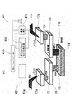
- 3 is performed by the magnetic memory manufacturing apparatus having a plurality of various forming apparatuses 51, the magnetic field heat treatment chamber 52, the heat treatment chamber 53, the control unit 54, and the like shown in FIG.
- Produced. 4 to 10 are diagrams for explaining an example of a detailed manufacturing method of the magnetic memory 10.
- the magnetic memory 10 is provided with a CMOS 13 on a wafer 12 as a substrate, and a multilayer intermediate wiring 14 (for example, M1-M4) on the CMOS 13. ) Is provided.
- a multilayer intermediate wiring 14 for example, M1-M4 on the CMOS 13.
- M1-M4 multilayer intermediate wiring 14
- an example of an intermediate wiring having four layers is shown.
- the total number of wirings can be changed according to the application of the MRAM, and the formation place of the MTJ element 11 is not necessarily limited to the M4 wiring. Is not to be done.
- An MTJ element 11 is provided on the intermediate wiring 14.
- the MTJ element 11 and the intermediate wiring 14 are electrically connected.
- An upper wiring 15 is provided above the MTJ element 11, and the MTJ element 11 and the upper wiring 15 are electrically connected.
- the lower electrode 140 is provided on the first interlayer film 1.
- the first interlayer film 1 is made of an insulating material and is disposed above a CMOS 13 provided on a wafer 12 as a substrate.
- the first interlayer film 1 is provided with a conductive via 141 (VIA), and the via 141 has a structure in which the lower electrode 140 and the CMOS 13 or the like are electrically connected.
- An MTJ element 11 having a first magnetic layer (conductive layer) as a reference layer 111 adjacent to the lower electrode 140, a barrier layer 112 as a nonmagnetic layer, and a second magnetic layer (conductive layer) as a recording layer 113 is provided. It has been.
- a conductive hard mask 103 is provided adjacent to the recording layer 113.
- a conductive via 151 and an upper wiring 15 are provided adjacent to the hard mask 103.
- a protective film 105 (capture film) is provided on the side surface side of the MTJ element 11 to protect the MTJ element 11.
- a second interlayer film 2 is provided around the protective film 105, and a diffusion prevention film 106 is provided between the second interlayer film 2 and the upper wiring 15.
- the first magnetic layer as the reference layer 111 and the second magnetic layer as the recording layer 113 are made of a material containing a ferromagnetic material such as an alloy containing Co, Fe, or Ni, for example, CoFeB.
- the barrier layer 112, which is a nonmagnetic layer, is made of a material having a compound such as MgO, Al 2 O 3 , SiO 2 , TiO, or HfO.
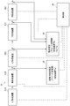
- the magnetic memory manufacturing apparatus includes a plurality of various forming apparatuses 51, a heat treatment chamber 52 in a magnetic field, a heat treatment chamber 53 as a magnetic field non-application annealing treatment chamber, and a control unit. 54 etc.
- the manufacturing apparatus may include an inspection apparatus that inspects a substrate or the like processed by each forming apparatus.
- the forming device 51 includes an A forming device 51A, a B forming device 51B, a C forming device 51C,..., A Y forming device 51Y, a Z forming device 51Z, and the like.
- each forming apparatus 51 includes a film forming apparatus such as a sputtering apparatus, a resist coating apparatus, an exposure apparatus, an etching apparatus, a chemical vapor deposition apparatus, a chemical mechanical polishing apparatus, a plating apparatus, a dicing apparatus, a die bonding apparatus, For example, a wire bonding apparatus or a resin sealing apparatus.
- the substrate is naturally or forcibly cooled to room temperature, and then annealed in a magnetic field.
- the processing chamber heat treatment chamber 52 in a magnetic field
- the magnetization of 111 is magnetized so as to be aligned in the perpendicular direction.
- the substrate provided with the MTJ element is processed according to the next process by the next forming apparatus.
- the room temperature is about 1 ° C. to 30 ° C.
- the heat treatment chamber 53 (magnetic field non-applied annealing treatment chamber) is an MTJ element formed on the substrate, a protective film (capturing film), etc., if necessary, after a forming process that generates a thermal history by various forming apparatuses 51.
- an annealing process is performed at the second processing temperature Tb to relieve stress or strain of the MTJ element and the protective film.
- the second processing temperature Tb is set to a temperature lower than the first processing temperature Ta.
- the control unit 54 comprehensively controls each forming device 51, a magnetic field heat treatment chamber 52 (magnetic field annealing treatment chamber), a heat treatment chamber 53 (annealing treatment chamber) as a magnetic field non-application annealing treatment chamber, and the like.
- a magnetic memory is manufactured.
- the control unit 54 is configured by a computer, and implements a magnetic memory manufacturing method and the like according to the present invention by executing a control program.
- a method for manufacturing a magnetic memory will be described.
- a wafer 12 such as silicon serving as a substrate is put into a predetermined forming apparatus 51 (step S11), a CMOS 13 is produced on the surface of the wafer 12 (step S12), and an MTJ is formed on the CMOS 13.
- a multilayer intermediate wiring 14 (for example, M1-M4) for connecting to the element 11 is formed.
- the first interlayer film 1 is formed on the intermediate wiring 14, and a via hole is formed in the first interlayer film 1 (see FIG. 4A).
- step S14 a conductive layer that becomes the lower electrode 140 adjacent to the first interlayer film 1 by a film forming apparatus, for example, a physical vapor deposition (PVD: Physical Vapor Deposition) apparatus, particularly in this embodiment, by a sputtering apparatus.
- a film forming apparatus for example, a physical vapor deposition (PVD: Physical Vapor Deposition) apparatus, particularly in this embodiment, by a sputtering apparatus.
- PVD Physical Vapor Deposition
- the first magnetic film to be the reference layer 111, the barrier layer 112 to be the nonmagnetic layer, the second magnetic film to be the recording layer 113, and the hard mask 103 are sequentially formed.
- heating from room temperature may be performed as necessary.
- a conductive material is formed in the via hole provided in the first interlayer film 1 and is electrically connected, so that the electrical connection with the via 141 (VIA) is achieved. Contact is formed.
- step S15 the wafer 12A (substrate) on which the magnetic film or the like is formed in the magnetic field heat treatment chamber 52 (magnetic field annealing treatment chamber) dedicated to the annealing treatment.
- the heat treatment chamber 52 in the magnetic field is provided with a heating unit 522 such as a heater, a temperature sensor 523, a vacuum pump 524, a magnetic field generator 525, and the like.
- the control unit 54 comprehensively controls each component of the heat treatment chamber 52 in the magnetic field.
- a wafer 12A (substrate) on which a magnetic film or the like is formed is disposed in the heat treatment chamber 52 in a room temperature state, and the heat treatment chamber 52 is evacuated by a vacuum pump 524. While the inside of the heat treatment chamber 52 is heated to the first processing temperature Ta (about 380 ° C. to 420 ° C., in this embodiment, 400 ° C.) by the heating unit 522, the first magnetic film serving as the reference layer 111 is heated by the magnetic field generator 525.
- Ta about 380 ° C. to 420 ° C., in this embodiment, 400 ° C.
- a magnetic field is applied in a direction perpendicular to the surface (orthogonal direction), and after a predetermined time has elapsed, the heating unit 522 is turned off, and after the temperature reaches about room temperature, the annealed substrate is removed from the heat treatment chamber 52. And the film
- the room temperature is about 1 ° C. to 30 ° C.
- step S16 the MTJ pattern 104 is produced by lithography.
- a photoresist is applied onto the hard mask 103 by a resist coating apparatus (the processing temperature is room temperature), and a baking process is performed on the photoresist (about 100 ° C.).
- the pattern of the photomask is transferred to the photoresist by the exposure apparatus (processing temperature is room temperature).
- a post-baking process is performed with respect to it, and an unexposed part is removed (about 150 degreeC).
- An inspection apparatus inspects the shape of the lithography.
- step S17 the hard mask and the MTJ are etched. Specifically, the substrate on which the MTJ pattern 104 or the like is formed is subjected to an etching process using a reactive ion etching apparatus (the processing temperature is room temperature), as shown in FIG. A hard mask 103 and an MTJ element 11 having a shape corresponding to 104 are formed. After removing the photoresist (MTJ pattern 104), the inspection apparatus inspects the shape of the MTJ element 11.
- a reactive ion etching apparatus the processing temperature is room temperature
- step S18 the substrate subjected to the process of step S17 is placed in the apparatus of the chemical vapor deposition apparatus, a reactive gas is introduced into the apparatus, and the substrate is heated to about 200 ° C. to 300 ° C.
- a protective film 105 (capture film) is formed on the conductive layer to be the lower electrode 140.
- the protective film 105 is formed on the side surface of the MTJ element 11 and adjacent to the hard mask 103.
- Examples of the material for forming the protective film 105 (capture film) include SiN.
- step S19 after the lower electrode resist pattern is formed on the substrate that has been subjected to the above processing, an etching process is performed using a reactive ion etching apparatus, as shown in FIG. 5C.
- the lower electrode 140 having the shape is formed.
- the processing temperature in step S19 is about room temperature.
- step S20 an annealing process (heat treatment) is performed on the substrate on which the above process has been performed.
- the heat treatment chamber 53 annealing chamber
- a heating unit 532 such as a heater, a temperature sensor 533, a vacuum pump 534, an inert gas supply unit 536, and the like. It has been.
- the control unit 54 comprehensively controls each component of the heat treatment chamber 53.
- the wafer 12B (substrate) subjected to the above treatment is disposed in the heat treatment chamber 53 in a state where no magnetic field is applied and in a room temperature state, and the inside of the heat treatment chamber 53 is processed by a vacuum pump 534.
- the inside of the heat treatment chamber 53 is heated to the second processing temperature Tb (for example, 200 ° C. to less than 400 ° C., in this embodiment, 300 ° C.) by the heating unit 532, and the heating unit 532 is turned off after a predetermined time.
- the annealed substrate is taken out from the heat treatment chamber 53.
- the performance of the MTJ element or the like is inspected by the inspection device.
- an inert gas such as nitrogen gas or argon gas may be supplied into the heat treatment chamber 53 by the inert gas supply unit 536, and the annealing treatment may be performed in a state where the heat treatment chamber 53 is filled with the inert gas. .
- step S21 a process for forming the second interlayer film 2 is performed. Specifically, the substrate subjected to the process of step S20 is placed in the apparatus of the chemical vapor deposition apparatus, a reactive gas is introduced into the apparatus, and the substrate is heated to about 200 ° C. to 300 ° C. As shown in FIG. 6B, the second interlayer film 2 is formed adjacent to the first interlayer film 1 and the protective film 105 (capture film).
- a process for flattening the second interlayer film 2 is performed. Specifically, the surface of the second interlayer film 2 is polished while applying an abrasive to the surface of the second interlayer film 2 by a chemical mechanical polishing (CMP) apparatus. As shown in FIG. 7A, the surface of the second interlayer film 2 becomes flat.
- the processing temperature of the planarization process is about room temperature.
- step S22 as shown in FIG. 7B, an annealing process is performed on the substrate on which the planarization process has been performed.
- a description of the configuration of the heat treatment chamber 53 (annealing chamber) is omitted.
- the annealing process is the same as in step S20.
- the wafer 12C (substrate) on which the above process has been performed is arranged in the heat treatment chamber 53 in a state where no magnetic field is applied and in a room temperature state, and the heat treatment chamber is placed.
- the inside of the heat treatment chamber 53 is heated to the second treatment temperature Tb (for example, 200 ° C. or more to less than 400 ° C., in this embodiment, 300 ° C.) by the heating unit 532 for a predetermined time.
- Tb for example, 200 ° C. or more to less than 400 ° C., in this embodiment, 300 ° C.
- the heating unit 532 is turned off, and after reaching room temperature, the substrate subjected to the annealing process is taken out from the heat treatment chamber 53. Then, the state of CMP flattening is inspected by an inspection apparatus.
- step S23 an upper wiring formation process is performed on the substrate processed in step S22.
- an upper wiring film forming process and an upper wiring patterning process are performed after a via (via hole) forming process and a diffusion prevention film forming process.
- a process of forming a via (via hole) in the second interlayer film 2 is performed. Specifically, after forming a lithography pattern corresponding to a via hole, an etching process is performed by a reactive ion etching apparatus to form a via hole 151H.
- the processing temperature of step S23 is about room temperature.
- a process for forming the diffusion prevention film 106 is performed. Specifically, a substrate on which the via hole 151H is formed is placed in the chemical vapor deposition apparatus, and a reactive gas is introduced into the apparatus while heating the substrate to about 200 ° C. to 300 ° C. As shown in FIG. 8B, a diffusion prevention film 106 is formed on the surface of the second interlayer film 2 and the inner surface of the via hole 151H. Examples of the material for forming the diffusion prevention film 106 include TiN. The processing temperature of this diffusion prevention film forming process is about 200 ° C. to 300 ° C.
- an upper wiring film to be the upper wiring 15 is formed adjacent to the diffusion prevention film 106 by an electroless plating apparatus.
- the processing temperature is about room temperature.
- Cu or the like can be used as a material for forming the upper wiring. Further, Cu or the like is deposited in the via hole 151H, whereby the via 151 is formed.
- the upper wiring patterning process is performed. Specifically, after forming a lithography pattern corresponding to the shape of the upper wiring, an etching process is performed on the upper wiring film by a reactive ion etching apparatus, so that a predetermined shape is obtained as shown in FIG. Upper wiring 15 is formed.
- the processing temperature of this upper wiring patterning process is about room temperature.
- step S24 as shown in FIG. 9B, an annealing process is performed on the substrate that has been subjected to the above process.
- a description of the configuration of the heat treatment chamber 53 (annealing chamber) is omitted.
- the annealing process is the same as steps S20 and S22.
- the wafer 12D (substrate) on which the above process has been performed is placed in the heat treatment chamber 53 in a magnetic field non-applied state and a room temperature state.
- the inside of the heat treatment chamber 53 is set to a vacuum state or an inert gas atmosphere, and the inside of the heat treatment chamber 53 is heated to a second treatment temperature Tb (for example, 200 ° C.
- Tb for example, 200 ° C.
- Steps S21 and S23 are referred to as a wiring formation process (BEOL: Back end of line).
- step S25 a packaging process is performed.
- chip cutting processing, chip die bonding processing, wire bonding processing, resin sealing processing, and the like are performed as the packaging processing.
- the wafer 12E (substrate) that has been subjected to the process up to step S24 is cut into a chip shape by a dicing apparatus, and a predetermined size is obtained.
- the chip 121 is manufactured.
- the processing temperature is room temperature.
- the diameter of the wafer is 300 mm.
- the chip 121 is bonded onto the circuit board via the bonding layer 201 made of a conductive adhesive material.
- the circuit board includes an insulating material 203, a metal pattern 202 as a circuit pattern, and a conductor 204 such as solder.
- the processing temperature of the chip die bonding process is about 150 ° C. to 200 ° C.
- a predetermined portion of the chip 121 and a predetermined portion of the metal pattern 202 of the circuit board are electrically connected by a wire bonding metal line 206.
- the chip 121 and the metal wire 206 on the circuit board are sealed with a resin material 207.
- the magnetic memory 10 is manufactured by the series of processes described above.
- the processing temperature of the bonding part is about 150 ° C. to 300 ° C.
- the chip is not heated.
- step S26 the magnetic memory 10 manufactured as described above is annealed as shown in FIG. A description of the configuration of the heat treatment chamber 53 (annealing chamber) is omitted.
- the annealing process is the same as steps S20, S22, and S24.
- the magnetic memory 10 is disposed in the heat treatment chamber 53 in a magnetic field non-applied state and a room temperature state, and the heat treatment chamber 53 is filled with the annealing process.
- a vacuum state or an inert gas atmosphere the inside of the heat treatment chamber 53 is heated to a second treatment temperature Tb (for example, 200 ° C.
- the heating unit 532 After the heating unit 532 is turned off and the temperature reaches about room temperature, the magnetic memory 10 subjected to the annealing process is taken out from the heat treatment chamber 53. Then, the various performances of the elements and the like are finally inspected by the inspection apparatus.
- a plurality of bit lines 18 are wired as the upper wiring 15 of the MTJ element 11, and a plurality of word lines 19 are formed above the CMOS 13. It consists of wired MRAM.
- the bit lines 18 are arranged in parallel to each other and are connected to the bit line selection circuit 18a.
- the word lines 19 are arranged in parallel to each other and connected to the word line selection circuit 19a.
- the bit line selection circuit 18a and the word line selection circuit 19a are used to generate predetermined bit lines 18 and This is performed by applying a voltage to the word line 19.
- the bit line selection circuit 18a and the word line selection circuit 19a select predetermined bit lines 18 and word lines 19 based on the read bit numbers, respectively, and sense amplifiers Connect to 20 and do.
- a reference resistor 8 is electrically connected to the sense amplifier.
- the annealing process in the heat treatment chamber 53 is performed by performing any one or more of steps S20, S22, S24, and S26 of the above-described magnetic memory manufacturing process, thereby allowing the MTJ element and the protective film (capture film). It is possible to relieve stress or strain.
- FIG. 12 is a diagram illustrating an example of a temporal change in temperature at the time of manufacturing a magnetic memory (semiconductor integrated circuit).
- the second treatment temperature Tb of the annealing treatment by the heat treatment chamber 53 is set lower than the first treatment temperature Ta in the magnetic field heat treatment step.
- the MTJ element and the protective layer (capture layer) Stress or strain can be reliably relieved. That is, stress or strain of a protective film (capture film), MTJ element, etc. can be relaxed without degrading the element performance of the MTJ element.
- the magnetic memory provided can be provided.
- the inventor of the present application actually manufactured a magnetic memory having a magnetic tunnel junction element (magnetoresistance effect element), and the thermal stability of the magnetoresistance effect element.
- the index ⁇ 0 was measured. If it is difficult to perform heat treatment (annealing without applying a magnetic field) in all the steps described so far (specifically, S20, S22, S24, and S26 shown in FIG. 3) due to restrictions on manufacturing costs, etc. It is effective to perform a heat treatment step (magnetic field non-applied annealing treatment step S24) after the step (S23) of forming the upper electrode (upper wiring 15) in which all the MRAM manufacturing steps are completed.
- a heat treatment step magnetic field non-applied annealing treatment step S24
- FIG. 13 is a flowchart showing an example of a method for manufacturing a magnetic memory according to an embodiment of the present invention.
- steps S11 to S19, S21, S23, and S24 are executed, and the effect of this step S24 (magnetic field non-application annealing treatment) is confirmed.
- Steps S20, S22, S25, and S26 shown in FIG. 3 are not executed.
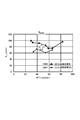
- FIG. 14 is a diagram showing an example of the thermal stability index of the MTJ element manufactured by the magnetic memory manufacturing method shown in FIG. 13 and the thermal stability index of the MTJ element of the comparative example.
- the thermal stability index was measured by the measurement system shown in FIG.
- the vertical axis indicates the thermal stability index ⁇ 0
- the horizontal axis indicates the size of the MTJ element.
- the size of the MTJ element is the diameter of the cylindrical recording layer.
- the triangular mark indicates the magnetic memory manufacturing method according to the embodiment of the present invention shown in FIG. 13, and more specifically, the magnetic field produced by executing steps S11 to S19, S21, S23, and S24 (annealing).
- the value of the thermal stability index of the MTJ element of the memory is shown. That is, after the BEOL process in steps S21 and S23, an annealing process in the heat treatment chamber 53 is performed.
- the circle mark indicates the method of manufacturing the magnetic memory of the comparative example, specifically, the value of the thermal stability index of the MTJ element of the magnetic memory manufactured by executing steps S11 to S19, S21, and S23. That is, in the comparative example, the annealing process by the heat treatment chamber 53 is not performed.
- the thermal stability index ⁇ 0 of the MTJ element manufactured by the magnetic memory manufacturing method according to the present invention showed a large value compared to the comparative example. That is, by performing the annealing process in the heat treatment chamber 53, the stress or strain of the protective film (capture film), the MTJ element or the like is relaxed, and the MTJ element having a high thermal stability index ⁇ 0 is manufactured. I understood that.
- the failure rate F of a magnetic memory with a capacity of m bits is expressed by Equation (4).
- Equation (5) the time t during which a failure rate 10 ⁇ 7 or less that can be remedied by a general error compensation circuit can be ensured is expressed by Equation (5).
- ⁇ 0 70 or so when the MTJ size is 40 nm, so the time t is about 0.1 year.
- the time t is about 6 ⁇ 10 7 years, and can be expanded dramatically.
- FIG. 15 is a conceptual diagram showing an example of a measurement system for measuring the thermal stability index of an MTJ element according to an embodiment of the present invention.
- an inspection terminal block 17 including an intermediate wiring 14, a via 16 (VIA), and an upper wiring 15 electrically connected only to the evaluation MTJ element 11 a is formed.
- the inspection terminal block 17 is composed of a pair of terminals.
- One terminal is an intermediate wiring 14 (BASE) connected to the lower part of a single evaluation MTJ element 11a and a via 16 formed thereon.
- the inspection terminal block 17 is configured to allow a current to flow only through a single evaluation MTJ element 11a that is electrically connected.
- the measurement system 40 includes a heat retaining unit (not shown), a measurement unit 41, and an analysis unit 42.
- the heat retaining means is composed of a temperature-adjustable prober, and is configured to be able to hold a wafer 12 including the evaluation MTJ element 11a so as to be maintained at a predetermined temperature.
- the measuring means 41 has a pair of probes 41a of a prober as a heat retaining means, for example, a voltage pulse generator 41b, a standard resistor 41c, and a voltage measuring instrument 41d.
- the voltage pulse generator 41b is connected to the probe 41a, and a voltage pulse can be applied between the probes 41a.
- the standard resistor 41c is connected in series between one probe 41a and the voltage pulse generator 41b.
- the voltage measuring device 41d is composed of a measuring device such as an oscilloscope capable of measuring a voltage, and is connected in parallel to the standard resistor 41c so that the voltage generated in the standard resistor 41c can be measured.
- a DC current source and a trigger mechanism that specifies timing for generating a current from the DC current source may be used.
- the measuring means 41 brings each probe 41a into contact with a pad 17a connected via a via (VIA) to the upper wiring 15 of each inspection terminal block 17 of the MTJ element 11a for evaluation, and a voltage pulse generator 41b is used to determine a predetermined value.
- the voltage pulse is generated and applied to both ends of the evaluation MTJ element 11a, so that a predetermined current flows through the evaluation MTJ element 11a.
- the voltage generated at both ends of the standard resistor 41c generated by the current is monitored and measured by the voltage measuring device 41d for a predetermined time, so that the change in the resistance value of the evaluation MTJ element 11a can be measured. ing.
- the analyzing means 42 is configured by a computer and is connected to the voltage measuring device 41d so that the measurement value of the voltage measuring device 41d can be input.
- the analyzing means 42 is configured to be able to calculate the time constant ⁇ p for holding the low resistance state and the time constant ⁇ AP for holding the high resistance state from the change in the resistance value measured by the voltage measuring device 41d.
- a resistance value change is measured for each current while a plurality of currents of different magnitudes are sequentially flowed, and the frequency distribution Np (t) of the time during which the low resistance state is maintained from the resistance value change, and obtains a high resistance state of the time for maintaining the frequency distribution N AP (t), respectively N p (t) ⁇ exp (-t / ⁇ p), and N AP (t) ⁇ exp (-t / ⁇ AP) Is used to calculate the time constant ⁇ p for maintaining the low resistance state and the time constant ⁇ AP for maintaining the high resistance state.
- the thermal stability index ⁇ 0 and I c0 are expressed by Equation (6). calculate.
- the measurement method of the thermal stability index ⁇ 0 by the measurement system shown in FIG. 15 has been described.
- the measurement method is not limited to this, and if the thermal stability index of the MTJ element can be measured, for example, Measurement methods such as a magnetic field pulse method and a current pulse method may be employed.
- the manufacturing method of the magnetic memory including the magnetic tunnel junction element (magnetoresistance effect element) includes the steps after the heat treatment process in the magnetic field at the first processing temperature Ta.
- a heat treatment chamber In 53 annealing chamber
- annealing is performed on the substrate on which the MTJ element, the protective film, etc. are formed at the second processing temperature Tb in a magnetic field non-applied state, in a vacuum or in an inert gas atmosphere.
- the second processing temperature Tb ⁇ the first processing temperature Ta.
- the first magnetic layer (reference layer 111) is provided on the substrate provided with the electrode layer (140).
- Forming a magnetic film having a nonmagnetic layer (barrier layer 112) between the first magnetic layer (recording layer 113) and the first magnetic layer see A magnetic field annealing process (S15) in which a magnetic field is applied in a direction perpendicular to the film surface of the layer 111) or the second magnetic layer (recording layer 113) and annealing is performed at the first processing temperature Ta, and is formed on the substrate.
- Etching the magnetic film to form a magnetic tunnel junction element (MTJ element 11) having a predetermined pattern (S17), and a protective film for protecting the magnetic tunnel junction element (MTJ element 11) formed on the substrate 105 (Cap A protective film forming step (S18) for forming a thermal insulation film), and forming a component of the magnetic memory on the substrate on which the protective film is formed after the protective film forming step (S18).
- the first processing temperature Ta is applied to the substrate in a vacuum or in an inert gas and without applying a magnetic field.
- a magnetic field non-application annealing process (at least one of S20, S22, S24, and S26) in which annealing is performed at a lower second processing temperature Tb.
- the constituent element of the magnetic memory is formed on the substrate on which the protective film 105 is formed after the protective film forming step (S18).
- the sealing portion resin material 207 for sealing the substrate on which the magnetoresistive effect element (magnetic tunnel junction element) is formed, and the like.
- the substrate (wafer) on which the magnetic tunnel junction element (MTJ element 11) and the protective film 105 are formed is annealed at the second processing temperature Tb, so that at least The stress or strain of the protective film 105 and the magnetic tunnel junction element (MTJ element 11) is relaxed, and a magnetic memory including a magnetic tunnel junction element with high element performance such as a thermal stability index can be easily manufactured.
- the basic element performance of the magnetic tunnel junction element (MTJ element 11) is substantially determined in the magnetic field annealing process (S15), but the subsequent lower electrode formation process (S19), the second interlayer film 2 The stress or strain of the protective film 105, the MTJ element 11, etc.
- the accumulated in the formation step (S21), the upper electrode (upper wiring) formation step (S23), the packaging step (S25), etc. is applied by the magnetic field non-application annealing treatment step.
- the device performance of the MTJ device 11 can be recovered.
- the annealing process at the relatively low second processing temperature Tb in the magnetic field non-application annealing process the performance of the magnetic tunnel junction element (MTJ element 11) itself is not deteriorated.
- the lower electrode in the formation process with thermal history, is formed by etching the electrode layer provided on the substrate to form a lower electrode having a predetermined pattern.
- Step (S19) is included.
- the substrate on which the lower electrode formation process (S19) has been performed is processed. That is, even if stress is generated in the protective film 105 and the MTJ element 11 after the lower electrode forming process (S19), the protective film 105 and the MTJ element 11 are subjected to the magnetic field non-application annealing process (S20). Such stress or strain can be easily relieved.
- the formation process with thermal history includes an interlayer film formation process (S21) for forming the second interlayer film 2.
- the substrate on which the interlayer film forming process (S21) for forming the second interlayer film 2 has been performed is processed. That is, after the interlayer film forming step (S21) for forming the second interlayer film 2, even if stress is generated in the protective film 105, the MTJ element 11, etc., the magnetic field non-application annealing treatment step (S22) The stress or strain of the protective film 105, the MTJ element 11, etc. can be easily relaxed.
- the formation step with thermal history includes an upper electrode formation step (S23) for forming the upper wiring 15 which is the upper electrode adjacent to the magnetic tunnel junction element.
- the substrate on which the upper electrode forming process (S23) has been performed is processed. That is, after the step of forming the upper electrode (upper wiring 15) (S23), even if stress is generated in the protective film 105, the MTJ element 11, etc., the magnetic field non-application annealing treatment step (S24) The stress or strain of the protective film 105, the MTJ element 11, etc. can be easily relaxed.
- the upper electrode (upper wiring 15) is formed by performing a heat treatment process (magnetic field non-application annealing process S24) after the process (S23) of forming the upper electrode (upper wiring 15) in which all the MRAM manufacturing processes are completed. Since all the processes with thermal history in the MRAM manufacturing process on the wafer have been completed by the process (S23), the stress of the protective film 105, the MTJ element 11, etc. accumulated before the magnetic field non-application annealing process S24 is completed. Or distortion can be alleviated at once.
- the forming process with thermal history includes a packaging process (S25) for performing a packaging process on the chip-shaped substrate including the magnetic tunnel junction element.
- the packaging step (S25) includes a step (S25) of resin-sealing in a state where a chip-like substrate including the magnetic tunnel junction element is bonded to the circuit substrate.
- the resin-sealed chip-like substrate is processed. That is, even if stress is generated in the protective film 105, the MTJ element 11, etc. after the packaging process (S25), the protective film 105, the MTJ element 11, etc. are obtained by the magnetic field non-application annealing process (S24). The stress or strain can be easily relieved.
- the annealing target object is naturally brought to room temperature immediately before the magnetic field non-application annealing process (at least one of S20, S22, S24, and S26). It has the process of cooling or forced cooling (refer FIG. 12). That is, even if stress is generated in the protective film 105 and the MTJ element 11 by being cooled to room temperature after each forming process, the protective film 105 and the MTJ element are subjected to the magnetic field non-application annealing process. The stress or strain can be relaxed to 11 grade.
- cooling to room temperature means cooling to about 1 ° C. to 30 ° C.
- the first treatment temperature Ta is 380 ° C. to 420 ° C., preferably 390 ° C. to 410 ° C., and optimally 400 ° C.
- the second processing temperature Tb lower than the first processing temperature Ta is 200 ° C. or higher and lower than 400 ° C., preferably 290 ° C. to 310 ° C., and optimally 300 ° C.
- the first processing temperature and the second processing temperature can be appropriately set according to the material and structure of the magnetic film and the nonmagnetic film.
- a magnetic field heat treatment chamber 52 in which the magnetic field generator is turned off may be used. Further, the reference layer 111 and the recording layer 113 of the MTJ element 11 may be arranged in reverse.
- the annealing process (heat treatment) of steps S20, S22, S24, and S26 is performed. It is not limited to form. For example, any one or more annealing processes (heat treatments) among steps S20, S22, S24, and S26 may be performed. Moreover, it is not necessary to perform all of steps S19, S21, S23, and S25, and any one or more steps may be performed as appropriate.
- Magnetic memory semiconductor integrated circuit
- MTJ element magnetoresistance effect element, magnetic tunnel junction element
- Wafer substrate
- CMOS complementary metal-oxide-semiconductor
- Intermediate wiring 15
- Sense amplifier 40
- Measurement system 41
- Measurement means 42 ... Analysis means 50
- Formation apparatus 52 Heat treatment chamber in magnetic field (anneal in magnetic field) Processing room) 53. Heat treatment chamber (magnetic field non-applied annealing chamber) 54.
- Control unit control device
- Protective film (capturing film) 106 Diffusion prevention film 111 ... Reference layer (first magnetic layer) 112 ... Barrier layer (nonmagnetic layer) 113 ... Recording layer (second magnetic layer) 140 ... lower electrode 141 ... via (VIA) 207 ... Resin material
Landscapes
- Engineering & Computer Science (AREA)
- Manufacturing & Machinery (AREA)
- Mram Or Spin Memory Techniques (AREA)
- Hall/Mr Elements (AREA)
Abstract
高い素子性能を有する磁気トンネル接合素子を備える磁気メモリを簡単に製造可能な磁気メモリの製造方法を提供する。磁気トンネル接合素子を備える磁気メモリの製造方法は、電極層が設けられた基板に、第1磁性層と第2磁性層との間に非磁性層を備えた磁性膜を形成する工程と、真空中で第1磁性層又は第2磁性層の膜面垂直方向に磁界を印加した状態で、第1処理温度でアニール処理を行う磁場中アニール処理工程と、磁気トンネル接合素子を形成する工程と、磁気トンネル接合素子を保護する保護膜を形成する保護膜形成工程と、保護膜形成工程の後に、保護膜が形成された基板に対して、磁気メモリの構成要素を形成する、熱履歴を伴う形成工程と、アニール処理室にて、真空中又は不活性ガス中、磁場非印加状態で、基板に対して、第1処理温度よりも低い第2処理温度でアニール処理を施す磁場非印加アニール処理工程と、を有する。
Description
本発明は、磁気トンネル接合素子を備える磁気メモリの製造方法に関する。
磁気抵抗効果素子を用いたMRAM等の不揮発メモリが知られている(例えば、特許文献1参照)。磁気抵抗効果素子としては、例えば、図16に示したように、磁性層である参照層111と記録層113の間に障壁層112(非磁性障壁層)を配置した磁気トンネル接合素子(MTJ素子)を挙げることができる。図16に示した例では、磁化の向きが変化しにくい参照層111は、層面(膜面)に対して垂直方向に磁化されている。記録層113は磁化方向が可変である。記録層113の飽和磁化Msは記録層113の材料、構造、温度等により規定されている。図16に示した磁気抵抗効果素子を、いわゆる垂直磁化MTJ素子という。記録層113の磁化方向が、参照層111の磁化に対して平行である場合にMTJ素子の電気抵抗が低くなり、反平行である場合にMTJ素子の電気抵抗が高くなる。MTJ素子は2つの抵抗の状態を、ビット情報の“0”及び“1”にそれぞれ対応させることで情報を記録可能な構造となっている。
図16、図17(a)に示したように、記録層113のエネルギーEbは、記録層113の磁化の方向と参照層111の磁化の方向とのなす角度θ、参照層111の磁気異方性エネルギー密度Keff、記録層113の体積Vを用いて、数式(1)で示される。sin2θ=1のとき(θ=90°、270°のとき)、磁化反転に要するエネルギー障壁(Eb)となる。
Eb=KeffVsin2θ ・・・(1)
磁気抵抗効果素子(MTJ素子)を有するMRAM等の不揮発性メモリについて、ビット情報の安定性を示すものとして、熱安定性指数がある。この熱安定性指数Δ0は、ボルツマン定数kB、絶対温度Tを用いて、数式(2)で表される。
Δ0=Eb/(kBT) ・・・(2)
熱安定性指数Δ0を有する記録層が、時間tののち磁化反転する確率Pは、Neel-Arrheniusの法則により、数式(3)で表される(例えば、非特許文献1参照)。図17(b)に示すように、確率Pが50%のときの時間tは、記録層113による情報の保持時間に対応する。
P=1-exp{(-t/10-9)×exp(-Δ0)} ・・・(3)
熱安定性指数Δ0を測定する一般的な方法として、磁場パルス法、電流パルス法などが知られている。磁場パルス法は、特定のパルス幅の磁場パルスを与えたときの磁化反転確率を、磁場パルスの磁場の大きさを変えながら測定し、磁場の大きさと磁化反転確率との関係に基づいて、熱安定性指数Δ0を求めるものである。
電流パルス法は、特定のパルス幅の電流パルスを与えたときの磁化反転確率を、電流パルスの電流の大きさを変えながら測定し、電流の大きさと磁化反転確率の関係に基づいて、熱安定性指数Δ0を求めるものである。
電流パルス法は、特定のパルス幅の電流パルスを与えたときの磁化反転確率を、電流パルスの電流の大きさを変えながら測定し、電流の大きさと磁化反転確率の関係に基づいて、熱安定性指数Δ0を求めるものである。
磁場パルス法や電流パルス法とは異なる熱安定性指数Δ0の測定方法として、10Mb以上のMTJからなるMRAMチップを準備し、各MTJの記録層にチェッカーボードパターン等で、1または0の情報を書き込み、高温で数分から100時間程度放置した後、初期情報がどのくらい失われたかを表すエラー率(error rate)を測定し、そのエラー率から算出した反転確率と放置時間との関係に基づいて、熱安定性指数Δ0を求める方法が知られている。この方法によれば、測定中にエネルギー障壁の値が変化しないため、磁化反転のモードによらず、正確な熱安定性指数Δ0を求めることができる。
ところで、磁気抵抗効果素子を用いた磁気メモリの製造方法としては、例えば、基板となるウェハにCMOSを作製し、CMOS上にMTJと接続するための中間配線を形成し、中間配線の上部に磁性膜を配線し、それらに対して磁場中熱処理を施した後、MTJパターンを作製し、エッチング加工によりMTJを形成し、保護膜を形成し、MTJ上に上部配線を形成し、それをチップ状に切り出し、ワイヤボンディング金属線で所定の回路基板に接続した後、樹脂封止を行う方法が知られている。
W.F. Brown, Jr.,"Thermal Fluctuations of a Single-Domain Particle",Phys. Rev., 1963, Vol.130, Num.5, p.1677-1686
しかしながら、上述した磁気メモリの製造方法では、磁性膜を形成した後、保護膜や配線等を形成する工程、樹脂封止工程等で、MTJ素子等に対して様々な熱履歴がかかり、MTJ素子やその周辺の構成要素に応力ないし歪が生じ、その応力ないし歪によりMTJ素子の熱安定性指数等の性能が劣化する場合がある。
また、特許文献2には、ブリッジ状に組んだ磁気検出素子を基板に形成するとともに、前記磁気検出素子を保護する保護膜を前記基板に形成することで該基板を多層基板とし、当該保護膜において前記磁気検出素子の近傍に、該保護膜をエッチングすることで応力緩和溝を形成し、該応力緩和溝形成後の前記多層基板をパッケージする工程手順を経る磁気センサの製造方法において、前記多層基板をパッケージする前に、該多層基板をアニールする、磁気センサの製造方法が記載されている。
しかしながら、特許文献2に記載の磁気センサの製造方法では、応力緩和溝を形成する煩雑な工程を行うことを要する。上記特許文献2に記載のように、パッケージ前にアニールした場合では、パッケージ後に残っている応力を除去することができない。
しかしながら、特許文献2に記載の磁気センサの製造方法では、応力緩和溝を形成する煩雑な工程を行うことを要する。上記特許文献2に記載のように、パッケージ前にアニールした場合では、パッケージ後に残っている応力を除去することができない。
本発明の磁気トンネル接合素子(磁気抵抗効果素子)を備える磁気メモリの製造方法は、少なくとも以下の構成を具備するものである。
磁気トンネル接合素子(磁気抵抗効果素子)を備える磁気メモリの製造方法であって、
電極層が設けられた基板に、第1磁性層と第2磁性層との間に非磁性層を備えた磁性膜を形成する工程と、
前記基板に対して、真空中で前記第1磁性層又は第2磁性層の膜面垂直方向に磁界を印加した状態で、第1処理温度でアニール処理を行う磁場中アニール処理工程と、
前記基板に形成された前記磁性膜にエッチング処理を施して所定のパターンの磁気トンネル接合素子を形成する工程と、
前記基板に形成された前記磁気トンネル接合素子を保護する保護膜を形成する保護膜形成工程と、
前記保護膜形成工程の後に、前記保護膜が形成された基板に対して、磁気メモリの構成要素を形成する、熱履歴を伴う形成工程と、
アニール処理室にて、真空中又は不活性ガス中、磁場非印加状態で、前記基板に対して、前記第1処理温度よりも低い第2処理温度でアニール処理を施す磁場非印加アニール処理工程と、を有することを特徴とする。
本発明に係る磁気トンネル接合素子を用いた磁気メモリの製造方法は、高い素子性能(熱安定性指数等)を有する磁気トンネル接合素子を備える磁気メモリを、簡単に製造することができる。
本発明の実施形態に係る磁気抵抗効果素子(磁気トンネル接合素子(MTJ素子))を用いた磁気メモリの製造方法は、基板にMTJ素子の磁性膜を形成し、その基板に対して第1処理温度Taで磁場中熱処理を施した後、それよりも後の工程のうち、MTJ素子を保護するSiN等の保護膜(キャプチュレーション膜)形成工程、第2層間膜形成工程、上部配線形成工程、パッケージング工程の少なくともいずれか一つ以上の工程の後、アニール処理室(熱処理室)内で、磁場非印加状態、真空中又は不活性ガス雰囲気中、第2処理温度Tbで、基板に対してアニール処理を施すことにより、保護膜(キャプチュレーション膜)やMTJ素子の応力ないし歪を緩和する。第2処理温度Tbは第1処理温度Taよりも低い温度に設定されている。
以下、図面を参照しながら本発明の実施形態を説明する。本発明の実施形態は図示の内容を含むが、これのみに限定されるものではない。なお、以後の各図の説明で、既に説明した部位と共通する部分は同一符号を付して重複説明を一部省略する。
図1に示したように、本発明の実施形態に係る磁気トンネル接合素子を用いた磁気メモリ10(半導体集積回路)は、多数のMTJ素子11(磁気トンネル接合素子)を有するMRAM(磁気メモリ)から成り、図2に示した複数の各種の形成装置51、磁場中熱処理室52、熱処理室53、制御部54等を有する磁気メモリの製造装置により、図3に示した製造工程を行うことにより作製される。図4~図10は、磁気メモリ10の詳細な製造方法の一例を説明するための図である。
本実施形態では、図1(a)に示したように、磁気メモリ10は、基板としてのウェハ12上にCMOS13が設けられており、そのCMOS13上に多層の中間配線14(例えば、M1-M4)が設けられている。本実施例では、4層からなる中間配線の例を示したが、配線の総数は、MRAMの応用に応じて変えることが可能で、またMTJ素子11の形成場所も、必ずしもM4配線上に限定されるものではない。中間配線14上にはMTJ素子11が設けられている。MTJ素子11と中間配線14は電気的に接続されている。MTJ素子11の上部には上部配線15が設けられており、MTJ素子11と上部配線15が電気的に接続されている。
詳細には、図1(b)に示したように、第1層間膜1上に下部電極140が設けられている。第1層間膜1は、絶縁性材料により形成されており、基板としてのウェハ12に設けられたCMOS13の上方に配置されている。第1層間膜1には導電性のビア141(VIA)が設けられており、ビア141は下部電極140とCMOS13等とを電気的に接続した構造を有する。下部電極140に隣接した参照層111としての第1磁性層(導電性層)、非磁性層の障壁層112、記録層113としての第2磁性層(導電性層)を有するMTJ素子11が設けられている。その記録層113に隣接して導電性のハードマスク103が設けられている。ハードマスク103に隣接して導電性のビア151、上部配線15が設けられている。
また、MTJ素子11の側面側には、保護膜105(キャプチュレーション膜)が設けられており、MTJ素子11を保護する構造となっている。また、保護膜105の周囲には第2層間膜2が設けられており、第2層間膜2と上部配線15との間には、拡散防止膜106が設けられている。
参照層111としての第1磁性層や記録層113としての第2磁性層は、例えば、Co、Fe、Niを含む合金、例えばCoFeB、などの強磁性体を含む材料で構成されている。
非磁性層である障壁層112は、例えば、MgO、Al2O3、SiO2、TiO、HfOなどの化合物を有する材料で構成されている。
また、MTJ素子11の側面側には、保護膜105(キャプチュレーション膜)が設けられており、MTJ素子11を保護する構造となっている。また、保護膜105の周囲には第2層間膜2が設けられており、第2層間膜2と上部配線15との間には、拡散防止膜106が設けられている。
参照層111としての第1磁性層や記録層113としての第2磁性層は、例えば、Co、Fe、Niを含む合金、例えばCoFeB、などの強磁性体を含む材料で構成されている。
非磁性層である障壁層112は、例えば、MgO、Al2O3、SiO2、TiO、HfOなどの化合物を有する材料で構成されている。
図2に示したように、本発明の実施形態に係る磁気メモリの製造装置は、複数の各種の形成装置51、磁場中熱処理室52、磁場非印加アニール処理室としての熱処理室53、制御部54等を有する。また、製造装置は、各形成装置により処理された基板等を検査する検査装置を備えていてもよい。
本実施形態では、形成装置51は、A形成装置51A、B形成装置51B、C形成装置51C、・・・、Y形成装置51Y、Z形成装置51Z等を有する。具体的には、各形成装置51は、スパッタリング装置等の製膜装置、レジスト塗布装置、露光装置、エッチング装置、化学気相成長装置、ケミカルメカニカルポリッシング装置、メッキ装置、ダイシング装置、ダイボンディング装置、ワイヤボンディング装置、樹脂封止装置などである。
基板に参照層111である第1磁性層、非磁性の障壁層112、記録層113である第2磁性層が形成された後、その基板を室温まで自然冷却または強制冷却した後、磁場中アニール処理室(磁場中熱処理室52)は、真空状態で、その基板に対して、第1処理温度Taにてアニール処理を行いつつ、参照層111の面直方向に磁界を印加して、参照層111の磁化を面直方向に揃えるように着磁させる。そのMTJ素子を備える基板は、次の形成装置により、次の工程に応じた処理が行われる。なお、本実施形態では、室温は1℃~30℃程度であるとする。
熱処理室53(磁場非印加アニール処理室)は、各種形成装置51による、熱履歴を生じる形成処理後、必要に応じて、基板上に形成されたMTJ素子や保護膜(キャプチュレーション膜)等に対して、第2処理温度Tbでアニール処理が施され、MTJ素子や保護膜の応力ないし歪を緩和する。なお、第2処理温度Tbは、第1処理温度Taよりも低い温度に設定されている。
制御部54(制御装置)は、各形成装置51、磁場中熱処理室52(磁場中アニール処理室)、磁場非印加アニール処理室としての熱処理室53(アニール処理室)等を統括的に制御することで、磁気メモリを製造する。詳細には、制御部54は、コンピュータにより構成され、制御プログラムを実行することにより、本発明に係る磁気メモリの製造方法等を実現する。
次に、本発明の実施形態に係る磁気メモリの製造方法を説明する。
図3に示すように、基板となるシリコン等のウェハ12を所定の形成装置51内に投入し(ステップS11)、そのウェハ12の表面にCMOS13を作製し(ステップS12)、CMOS13の上にMTJ素子11と接続するための多層の中間配線14(例えば、M1-M4)を形成する。
そして、中間配線14上に第1層間膜1が形成され、第1層間膜1にビアホールが形成される(図4(a)を参照)。
図3に示すように、基板となるシリコン等のウェハ12を所定の形成装置51内に投入し(ステップS11)、そのウェハ12の表面にCMOS13を作製し(ステップS12)、CMOS13の上にMTJ素子11と接続するための多層の中間配線14(例えば、M1-M4)を形成する。
そして、中間配線14上に第1層間膜1が形成され、第1層間膜1にビアホールが形成される(図4(a)を参照)。
次に、ステップS14において、製膜装置、例えば物理蒸着(PVD:Physical Vapor Deposition)装置、特に本実施形態では、スパッタリング装置により、第1層間膜1に隣接して、下部電極140となる導電層、参照層111となる第1磁性膜、非磁性層である障壁層112、記録層113となる第2磁性膜、ハードマスク103を順に成膜する。上記の製膜工程では、必要に応じて室温からの加熱を行う場合もある。尚、下部電極140となる導電層の形成時に、第1層間膜1に設けられたビアホールに、導電材料が成膜され、電気的に接続されることにより、ビア141(VIA)との電気的なコンタクトが形成される。
次に、ステップS15において、図4(b)に示したように、アニール処理専用の磁場中熱処理室52(磁場中アニール処理室)にて、上記磁性膜等が形成されたウェハ12A(基板)に対して、磁場中アニール処理が施される。詳細には、磁場中熱処理室52には、ヒーター等の加熱部522、温度センサ523、真空ポンプ524、磁場発生装置525などが設けられている。制御部54は、磁場中熱処理室52の各構成要素を統括的に制御する。
磁場中アニール処理としては、具体的には、室温状態の熱処理室52内に、磁性膜等が形成されたウェハ12A(基板)が配置され、真空ポンプ524により熱処理室52内を真空状態とし、加熱部522により熱処理室52内を第1処理温度Ta(380℃~420℃程度、本実施形態では400℃)に加熱しつつ、磁場発生装置525により、参照層111となる第1磁性膜の面に対して垂直方向(直交方向)に磁界を印加し、所定時間経過後、加熱部522をオフ状態とし、室温程度となった後、熱処理室52からアニール処理された基板を取り出す。そして、検査装置により磁性膜の膜性能を検査する。なお、本実施形態では、室温は1℃~30℃程度であるとする。
ステップS16において、図4(c)に示したように、MTJパターン104がリソグラフィで作製される。詳細には、レジスト塗布装置によりフォトレジストをハードマスク103上に塗布し(処理温度は室温)、それに対してベーキング処理を行う(約100℃)。次に、露光装置により、フォトマスクのパターンをフォトレジストに転写する(処理温度は室温)。次に、それに対してポストベーキング処理を施して、未露光部分を除去する(約150℃)。検査装置がリソグラフィの形状を検査する。
ステップS17において、ハードマスクとMTJに対して、エッチング処理を行う。詳細には、上記MTJパターン104等が形成された基板に対して、反応性イオンエッチング装置によりエッチング処理を施すことにより(処理温度は室温)、図5(a)に示したように、MTJパターン104に対応した形状のハードマスク103とMTJ素子11が形成される。フォトレジスト(MTJパターン104)を除去した後、検査装置がMTJ素子11の形状を検査する。
ステップS18において、化学気相成長装置の装置内に、ステップS17の処理が施された基板を配置し、装置内に反応性ガスを導入して、基板を200℃~300℃程度に加熱し、図5(b)に示すように、下部電極140となる導電層上に、保護膜105(キャプチュレーション膜)を成膜する。詳細には、MTJ素子11の側面側、及びハードマスク103に隣接して保護膜105が形成される。保護膜105(キャプチュレーション膜)の形成材料としては、例えばSiN等を挙げることができる。
ステップS19において、上記処理が行われた基板に対して、下部電極レジストパターンを形成後、反応性イオンエッチング装置を用いてエッチング処理を施すことにより、図5(c)に示したように、所定の形状の下部電極140が形成される。ステップS19における処理温度は、室温程度である。
ステップS20において、上記処理が行われた基板に対して、アニール処理(熱処理)を施す。詳細には、図6(a)に示したように、熱処理室53(アニール処理室)には、ヒーター等の加熱部532、温度センサ533、真空ポンプ534、不活性ガス供給部536などが設けられている。制御部54は、熱処理室53の各構成要素を統括的に制御する。
アニール処理としては、具体的には、磁場非印加状態、且つ、室温状態の熱処理室53内に、上記処理が行われたウェハ12B(基板)が配置され、真空ポンプ534により熱処理室53内を真空状態とし、加熱部532により熱処理室53内を第2処理温度Tb(例えば200℃以上~400℃未満、本実施形態では300℃)に加熱し、所定時間経過後、加熱部532をオフ状態とし、室温程度となった後、熱処理室53からアニール処理が行われた基板を取り出す。そして、検査装置によりMTJ素子等の性能を検査する。
MTJ素子や保護膜105等が形成されたウェハ12B(基板)に対して、上記アニール処理を施すことにより、MTJ素子や保護膜105等の応力ないし歪が緩和される。
MTJ素子や保護膜105等が形成されたウェハ12B(基板)に対して、上記アニール処理を施すことにより、MTJ素子や保護膜105等の応力ないし歪が緩和される。
尚、不活性ガス供給部536により窒素ガスやアルゴンガス等の不活性ガスを、熱処理室53内に供給し、熱処理室53内を不活性ガスで満たした状態で、アニール処理を施してもよい。
ステップS21において、第2層間膜2を形成する処理を行う。詳細には、化学気相成長装置の装置内に、ステップS20の処理が施された基板を配置し、装置内に反応性ガスを導入して、基板を200℃~300℃程度に加熱しながら成膜し、図6(b)に示したように、第1層間膜1や保護膜105(キャプチュレーション膜)に隣接して第2層間膜2が形成される。
次に、第2層間膜2を平坦化する処理を行う。詳細には、ケミカルメカニカルポリッシング(CMP)装置により、研磨剤を第2層間膜2の表面に塗布しながら、第2層間膜2の表面を研磨する処理を行う。図7(a)に示したように、第2層間膜2の表面が平坦となる。平坦化処理の処理温度は室温程度である。
ステップS22において、上記平坦化処理が行われた基板に対して、図7(b)に示したように、アニール処理を行う。熱処理室53(アニール処理室)の構成に関する説明は省略する。アニール処理としては、ステップS20と同様であり、具体的には、磁場非印加状態、且つ、室温状態の熱処理室53内に、上記処理が行われたウェハ12C(基板)が配置され、熱処理室53内を真空状態、又は不活性ガス雰囲気とし、加熱部532により熱処理室53内を第2処理温度Tb(例えば200℃以上~400℃未満、本実施形態では300℃)に加熱し、所定時間経過後、加熱部532をオフ状態とし、室温程度となった後、熱処理室53からアニール処理が行われた基板を取り出す。そして、検査装置によりCMPの平坦化の状況を検査する。
ステップS23において、上記ステップS22により処理された基板に対して、上部配線形成処理を行う。本実施形態では、ビア(ビアホール)形成処理、拡散防止膜形成処理の後、上部配線膜形成処理、上部配線パターンニング処理を行う。
詳細には、先ず、図8(a)に示したように、第2層間膜2にビア(ビアホール)を形成する処理を行う。具体的には、ビアホールに対応するリソグラフィパターンを形成後、反応性イオンエッチング装置によりエッチング処理が行われ、ビアホール151Hが形成される。ステップS23の処理温度は室温程度である。
次に、拡散防止膜106を形成する処理を行う。詳細には、化学気相成長装置の装置内に、上記ビアホール151H等が形成された基板を配置し、装置内に反応性ガスを導入して、基板を200℃~300℃程度に加熱しながら成膜し、図8(b)に示すように、第2層間膜2の表面、及びビアホール151Hの内側面に拡散防止膜106が形成される。拡散防止膜106の形成材料としては、例えばTiN等を挙げることができる。この拡散防止膜形成処理の処理温度は、200℃~300℃程度である。
次に、図8(c)に示したように、無電解めっき装置により、拡散防止膜106に隣接して、上部配線15となる上部配線膜を形成する。処理温度は、室温程度である。上部配線の形成材料としては、例えば、Cu等を採用することができる。また、ビアホール151HにCu等が成膜されることで、ビア151が形成される。
次に、上部配線パターンニング処理を行う。詳細には、上部配線の形状に対応したリソグラフィパターンを形成後、反応性イオンエッチング装置により上部配線膜に対してエッチング処理を行うことで、図9(a)に示したように、所定形状の上部配線15が形成される。この上部配線パターンニング処理の処理温度は、室温程度である。
ステップS24において、上記処理が施された基板に対して、図9(b)に示したように、アニール処理を行う。熱処理室53(アニール処理室)の構成に関する説明は省略する。アニール処理としては、ステップS20、S22と同様であり、具体的には、磁場非印加状態、且つ、室温状態の熱処理室53内に、上記処理が行われたウェハ12D(基板)が配置され、熱処理室53内を真空状態、又は不活性ガス雰囲気とし、加熱部532により熱処理室53内を第2処理温度Tb(例えば200℃以上~400℃未満、本実施形態では300℃)に加熱し、所定時間経過後、加熱部532をオフ状態とし、室温程度となった後、熱処理室53からアニール処理が行われた基板を取り出す。そして、検査装置によりMTJ素子等の性能を検査する。
尚、ステップS21、S23を配線形成工程(BEOL:Back end of line)という。
尚、ステップS21、S23を配線形成工程(BEOL:Back end of line)という。
ステップS25において、パッケージング処理を行う。本実施形態では、パッケージング処理としては、チップ切り出し処理、チップダイボンディング処理、ワイヤボンディング処理、樹脂封止処理等を行う。
詳細には、チップ切り出し処理としては、図9(c)に示したように、ステップS24までの処理が施されたウェハ12E(基板)を、ダイシング装置によりチップ状に切り出して、所定の大きさのチップ121を作製する。処理温度は室温である。本実施形態ではウェハの直径は300mmである。
チップダイボンディング処理としては、図10(a)に示したように、回路基板上に導電性接着材料からなるボンディング層201を介してチップ121を接着する。回路基板は、絶縁材203、回路パターンとしての金属パターン202、はんだ等の導電体204により構成されている。導電性接材料を用いた場合、チップダイボンディング処理の処理温度としては、150℃~200℃程度である。
ワイヤボンディング処理としては、図10(b)に示したように、チップ121の所定箇所と、回路基板の金属パターン202の所定箇所とをワイヤボンディング金属線206で電気的に接続する。
樹脂封止処理としては、図10(b)に示したように、回路基板上のチップ121及び金属線206を樹脂材料207により封止する。上記一連の処理により、磁気メモリ10が作製される。ボンディング部分の処理温度は150℃~300℃程度である。チップへの加熱は行わない。
ステップS26において、上記作製された磁気メモリ10に対して、図10(c)に示したように、アニール処理を行う。熱処理室53(アニール処理室)の構成に関する説明は省略する。アニール処理としては、ステップS20、S22、S24と同様であり、具体的には、磁場非印加状態、且つ、室温状態の熱処理室53内に、上記磁気メモリ10が配置され、熱処理室53内を真空状態、又は不活性ガス雰囲気とし、加熱部532により熱処理室53内を第2処理温度Tb(例えば200℃以上~400℃未満、本実施形態では300℃)に加熱し、所定時間経過後、加熱部532をオフ状態とし、室温程度となった後、熱処理室53からアニール処理が行われた磁気メモリ10を取り出す。そして、検査装置により最終的に素子等の各種の性能を検査する。
また、製造された磁気メモリ10(半導体集積回路)は、図11に示したように、MTJ素子11の上部配線15として複数のビット線18が配線され、CMOS13の上部に複数のワード線19が配線されたMRAMからなっている。各ビット線18は、互いに平行に配置され、ビットライン選択回路18aに接続されている。各ワード線19は互い平行に配置され、ワードライン選択回路19aに接続されている。
この磁気メモリ10(半導体集積回路)において、任意のMTJ素子11へ書き込みを行う場合、書き込みビットナンバーをもとに、ビットライン選択回路18aおよびワードライン選択回路19aでそれぞれ、所定のビット線18およびワード線19に電圧を印加して行う。
また、任意のMTJ素子11から読み出しを行う場合、読み出しビットナンバーをもとに、ビットライン選択回路18aおよびワードライン選択回路19aで、それぞれ所定のビット線18およびワード線19を選択し、センスアンプ20へ接続して行う。センスアンプには参照抵抗8が電気的に接続されている。
また、任意のMTJ素子11から読み出しを行う場合、読み出しビットナンバーをもとに、ビットライン選択回路18aおよびワードライン選択回路19aで、それぞれ所定のビット線18およびワード線19を選択し、センスアンプ20へ接続して行う。センスアンプには参照抵抗8が電気的に接続されている。
尚、熱処理室53によるアニール処理は、上述した磁気メモリの製造工程のステップS20、S22、S24、S26のうち、いずれか一つ以上を行うことで、MTJ素子や保護膜(キャプチュレーション膜)等の応力ないし歪を緩和することができる。
図12は磁気メモリ(半導体集積回路)製造時の温度の時間変化の一例を示す図である。
本実施形態では、熱処理室53(アニール処理室)による、アニール処理の第2処理温度Tbは、磁場中熱処理工程での第1処理温度Taよりも低く設定されている。
また、図12に示したように、アニール処理対象物を室温状態に自然冷却する、又は強制冷却した後、熱処理室53による磁場非印加のアニール処理を行うので、MTJ素子や保護層(キャプチュレーション膜)等の応力ないし歪を確実に緩和することができる。
すなわち、MTJ素子の素子性能を劣化させることなく、保護膜(キャプチュレーション膜)やMTJ素子等の応力ないし歪を緩和することができ、その応力ないし歪の緩和により、高い性能のMTJ素子を備えた磁気メモリを提供することができる。
本願発明者は、本発明に係る磁気メモリの製造方法の効果を確認するために、磁気トンネル接合素子(磁気抵抗効果素子)を有する磁気メモリを実際に作製し、磁気抵抗効果素子の熱安定性指数Δ0の測定を行った。尚、製造コスト等の制約で、これまで述べたすべての工程(詳細には図3に示すS20、S22、S24、S26)での熱処理(磁場非印加アニール処理)が難しい場合、ウェハ上でのMRAM製造工程がすべて終了する上部電極(上部配線15)を形成する工程(S23)の後に熱処理工程(磁場非印加アニール処理工程S24)を行うことが効果的である。この理由は、上部電極(上部配線15)を形成する工程(S23)までに、ウェハ上でのMRAM製造工程におけるすべての熱履歴を伴う工程が終了しているので、上部電極(上部配線15)を形成する工程(S23)の後に熱処理(磁場非印加アニール処理工程S24)を行うと、この工程以前に蓄積された保護膜105やMTJ素子11等の応力ないし歪を、一度に緩和することができるためである。
図13は本発明の一実施形態に係る磁気メモリの製造方法の一例を示すフローチャートである。図13に示した磁気メモリの製造方法では、ステップS11~S19、S21、S23、S24(磁場非印加アニール処理)を実行し、このステップS24(磁場非印加アニール処理)による効果を確認するために、図3に示したステップS20、S22、S25、S26に関しては実行していない。
図14は、図13に示した磁気メモリの製造方法により作製されたMTJ素子の熱安定性指数と、比較例のMTJ素子の熱安定性指数の一例を示す図である。熱安定性指数の測定は、図15に示した測定システムにより測定を行った。
図14において、縦軸に熱安定性指数Δ0を示し、横軸にMTJ素子のサイズを示す。MTJ素子のサイズは、本実施例では、円柱形状の記録層の直径としている。
図14は、図13に示した磁気メモリの製造方法により作製されたMTJ素子の熱安定性指数と、比較例のMTJ素子の熱安定性指数の一例を示す図である。熱安定性指数の測定は、図15に示した測定システムにより測定を行った。
図14において、縦軸に熱安定性指数Δ0を示し、横軸にMTJ素子のサイズを示す。MTJ素子のサイズは、本実施例では、円柱形状の記録層の直径としている。
三角マークは、図13に示した本発明の一実施形態に係る磁性メモリの製造方法、詳細には、ステップS11~S19、S21、S23、S24(アニール処理)を実行することにより作製された磁気メモリのMTJ素子の熱安定指数の値を示す。つまり、ステップS21、S23のBEOL工程後に、熱処理室53によるアニール処理を行っている。
丸マークは、比較例の磁性メモリの製造方法、詳細には、ステップS11~S19、S21、S23を実行することにより作製された磁気メモリのMTJ素子の熱安定指数の値を示す。つまり、比較例では、熱処理室53によるアニール処理を行っていない。
測定の結果、図14に示したように、本発明に係る磁気メモリの製造方法で製造されたMTJ素子の熱安定性指数Δ0は、比較例と比べて、大きな値を示した。つまり、熱処理室53によるアニール処理を施すことにより、保護膜(キャプチュレーション膜)やMTJ素子等の応力ないし歪が緩和されて、高い熱安定性指数Δ0を有するMTJ素子が作製されていることが分かった。
非特許文献2によると、数式(3)から、容量mビットの磁気メモリの故障率Fは、数式(4)で表される。
非特許文献2によると、数式(3)から、容量mビットの磁気メモリの故障率Fは、数式(4)で表される。
F=1-exp{-m×(t/10-9)×exp(-Δ0)} ・・・(4)
したがって、一般的なエラー補償回路で救済可能な故障率10-7以下を確保可能な時間tは、数式(5)で表される。
t={(-10-9)/m}×ln(1-10-7)×exp(Δ0) ・・・(5)
例えば、メモリの容量として、本発明の主要な応用であるm=64Mbのエンベデッドメモリを想定すると、比較例では、MTJサイズ40nmの場合Δ0=70程度なので、上記時間tは約0.1年であるが、本発明に係る磁気メモリでは、MTJサイズ40nmの場合Δ0=90程度なので、上記時間tは約6×10⁷年であり、飛躍的に拡大可能となる。
R. Takemura et al,"A 32-Mb SPRAM With 2T1R Memory Cell, Localized Bi-Directional Write Driver and '1’/'0' Dual-Array Equalized Reference Scheme,",IEEE JOURNAL OF SOLID-STATE CIRCUITS, VOL. 45, NO. 4, APRIL 2010
図15は本発明の一実施形態に係るMTJ素子の熱安定性指数を測定する測定システムの一例を示す概念図である。
図15に示した例では、評価用MTJ素子11aのみに電気的に接続された中間配線14とビア16(VIA)と上部配線15とからなる検査用端子ブロック17が形成されている。
検査用端子ブロック17は、一対の端子から構成されており、一方の端子は、単体の評価用MTJ素子11aの下部に接続された中間配線14(BASE)と、その上に形成されたビア16と、上部配線15とで構成されている。検査用端子ブロック17は、電気的に接続された単体の評価用MTJ素子11aのみに電流を流すように構成されている。
図15に示した例では、評価用MTJ素子11aのみに電気的に接続された中間配線14とビア16(VIA)と上部配線15とからなる検査用端子ブロック17が形成されている。
検査用端子ブロック17は、一対の端子から構成されており、一方の端子は、単体の評価用MTJ素子11aの下部に接続された中間配線14(BASE)と、その上に形成されたビア16と、上部配線15とで構成されている。検査用端子ブロック17は、電気的に接続された単体の評価用MTJ素子11aのみに電流を流すように構成されている。
<熱安定性指数の測定>
次に、単体の評価用MTJ素子11aに対する熱安定性指数の測定方法を説明する。
図15に示したように、測定システム40は、保温手段(不図示)と、測定手段41と、解析手段42とを有する。
保温手段は、温度調整可能なプローバからなり、評価用MTJ素子11aを含むウェハ12を搭載して、所定の温度に保持可能に構成されている。
測定手段41は、保温手段のプローバの一対の探針41aと、例えば、電圧パルス発生器41bと、標準抵抗41cと、電圧測定器41dとを有する。
電圧パルス発生器41bは、探針41aに接続され、各探針41aの間に電圧パルスを印加可能になっている。標準抵抗41cは、一方の探針41aと電圧パルス発生器41bとの間に直列に接続されている。
電圧測定器41dは、電圧を測定可能なオシロスコープなどの測定器からなり、標準抵抗41cに並列に接続されて、標準抵抗41cに発生する電圧を測定可能に構成されている。なお電圧パルス発生器41bの代わりに、例えば、DC電流源と、DC電流源から電流を発生させるタイミングを指定するトリガー機構とを用いてもよい。
測定手段41は、各探針41aを評価用MTJ素子11aの各検査用端子ブロック17の上部配線15にビア(VIA)を介して接続されたパッド17aに接触させ、電圧パルス発生器41bで所定の電圧パルスを発生して、評価用MTJ素子11aの両端に印加することにより、評価用MTJ素子11aに所定の電流を流すように構成されている。また、その電流によって発生する標準抵抗41cの両端に発生する電圧を、所定時間、電圧測定器41dでモニターして測定することにより、評価用MTJ素子11aの抵抗値の変化を測定可能に構成されている。
解析手段42は、コンピュータで構成され、電圧測定器41dに接続されて、電圧測定器41dの測定値を入力可能に構成されている。解析手段42は、電圧測定器41dで測定された抵抗値の変化から、低抵抗状態を保持する時定数τp、及び高抵抗状態を保持する時定数τAPを算出可能に構成されている。
詳細には、異なる大きさの複数の電流を順番に流しながら、各電流についてそれぞれ抵抗値の変化を測定し、抵抗値の変化から、低抵抗状態を保持する時間の頻度分布Np(t)、及び高抵抗状態を保持する時間の頻度分布NAP(t)を求め、それぞれNp(t)∝exp(-t/τp)、およびNAP(t)∝exp(-t/τAP)の関係を用いて、低抵抗状態を保持する時定数τp、及び高抵抗状態を保持する時定数τAPを算出する。
また、所定の電流Iと、低抵抗状態を保持する時定数τp、高抵抗状態を保持する時定数τAPに基づいて、数式(6)により、熱安定性指数Δ0、及びIc0を算出する。
τP/(τP+τAP)=1/[1+exp{-Δ0(2I/Ic0)}]・・・(6)
以上、図15に示した測定システムによる、熱安定性指数Δ0の測定方法を説明したが、この測定方法に限られるものではなく、MTJ素子の熱安定性指数を測定することができれば、例えば、磁場パルス法、電流パルス法などの測定方法を採用してもよい。
以上、説明したように、本発明の実施形態に係る磁気トンネル接合素子(磁気抵抗効果素子)を備える磁気メモリの製造方法は、第1処理温度Taの磁場中熱処理工程の後の工程のうち、MTJ素子を保護するSiN等の保護膜105(キャプチュレーション膜)形成工程、第2層間膜2形成工程、上部配線形成工程、パッケージング工程の少なくともいずれか一つ以上の工程の後、熱処理室53(アニール処理室)内で、磁場非印加状態、真空中又は不活性ガス雰囲気中、第2処理温度Tbで、MTJ素子や保護膜等が形成された基板に対してアニール処理を施すことにより、保護膜(キャプチュレーション膜)やMTJ素子の応力ないし歪を緩和する。第2処理温度Tb<第1処理温度Taである。
詳細には、本発明の実施形態に係る磁気トンネル接合素子(MTJ素子11)を備える磁気メモリの製造方法は、電極層(140)が設けられた基板に、第1磁性層(参照層111)と第2磁性層(記録層113)との間に非磁性層(障壁層112)を備えた磁性膜を形成する工程(S14)と、基板に対して、真空中で第1磁性層(参照層111)又は第2磁性層(記録層113)の膜面垂直方向に磁界を印加した状態で、第1処理温度Taでアニール処理を行う磁場中アニール処理工程(S15)と、基板に形成された磁性膜にエッチング処理を施して所定のパターンの磁気トンネル接合素子(MTJ素子11)を形成する工程(S17)と、基板に形成された磁気トンネル接合素子(MTJ素子11)を保護する保護膜105(キャプチュレーション膜)を形成する保護膜形成工程(S18)と、保護膜形成工程(S18)の後に、保護膜が形成された基板に対して、磁気メモリの構成要素を形成する、熱履歴を伴う形成工程(S19、S21、S23、S25)と、熱処理室53(磁場非印加アニール処理室)にて、真空中又は不活性ガス中、磁場非印加状態で、基板に対して、第1処理温度Taよりも低い第2処理温度Tbでアニール処理を施す磁場非印加アニール処理工程(S20、S22、S24、S26のうち少なくとも1つ以上)と、を有する。
尚、上記保護膜形成工程(S18)の後に、保護膜105が形成された基板に対して、磁気メモリの構成要素を形成する、熱履歴を伴う形成工程における、磁気メモリの構成要素としては、例えば、下部電極140、第2層間膜2、上部配線15、磁気抵抗効果素子(磁気トンネル接合素子)が形成されている基板を樹脂封止する封止部分(樹脂材料207)等のいずれか1つ又は複数である。
尚、上記保護膜形成工程(S18)の後に、保護膜105が形成された基板に対して、磁気メモリの構成要素を形成する、熱履歴を伴う形成工程における、磁気メモリの構成要素としては、例えば、下部電極140、第2層間膜2、上部配線15、磁気抵抗効果素子(磁気トンネル接合素子)が形成されている基板を樹脂封止する封止部分(樹脂材料207)等のいずれか1つ又は複数である。
すなわち、磁場非印加アニール処理工程で、少なくとも磁気トンネル接合素子(MTJ素子11)や保護膜105が形成された基板(ウェハ)に対して、第2処理温度Tbでアニール処理を施すことにより、少なくとも保護膜105や磁気トンネル接合素子(MTJ素子11)の応力ないし歪が緩和され、熱安定性指数等の素子性能の高い、磁気トンネル接合素子を備える磁気メモリを簡単に製造することができる。
尚、上記磁場中アニール処理工程(S15)で、磁気トンネル接合素子(MTJ素子11)の基本的な素子性能が略決定されるが、その後の下部電極形成工程(S19)、第2層間膜2形成工程(S21)、上部電極(上部配線)形成工程(S23)、パッケージング工程(S25)等により蓄積される保護膜105やMTJ素子11等の応力ないし歪を、磁場非印加アニール処理工程により緩和させることで、MTJ素子11の素子性能の回復を図ることができる。
また、磁場非印加アニール処理工程で、比較的低い第2処理温度Tbでアニール処理を施すことにより、磁気トンネル接合素子(MTJ素子11)自体の性能劣化を生じさせない。
尚、上記磁場中アニール処理工程(S15)で、磁気トンネル接合素子(MTJ素子11)の基本的な素子性能が略決定されるが、その後の下部電極形成工程(S19)、第2層間膜2形成工程(S21)、上部電極(上部配線)形成工程(S23)、パッケージング工程(S25)等により蓄積される保護膜105やMTJ素子11等の応力ないし歪を、磁場非印加アニール処理工程により緩和させることで、MTJ素子11の素子性能の回復を図ることができる。
また、磁場非印加アニール処理工程で、比較的低い第2処理温度Tbでアニール処理を施すことにより、磁気トンネル接合素子(MTJ素子11)自体の性能劣化を生じさせない。
また、本発明の実施形態に係る磁気メモリの製造方法において、熱履歴を伴う形成工程は、基板に設けられた電極層にエッチング処理を施して、所定のパターンの下部電極を形成する下部電極形成工程(S19)を有する。磁場非印加アニール処理工程(S20)は、下部電極形成工程(S19)が施された基板に対して処理される。
すなわち、下部電極形成工程(S19)の後、保護膜105やMTJ素子11等に応力が生じている場合であっても、磁場非印加アニール処理工程(S20)により、保護膜105やMTJ素子11等の応力ないし歪を、簡単に緩和することができる。
すなわち、下部電極形成工程(S19)の後、保護膜105やMTJ素子11等に応力が生じている場合であっても、磁場非印加アニール処理工程(S20)により、保護膜105やMTJ素子11等の応力ないし歪を、簡単に緩和することができる。
また、本発明の実施形態に係る磁気メモリの製造方法において、熱履歴を伴う形成工程は、第2層間膜2を形成する層間膜形成工程(S21)を有する。磁場非印加アニール処理工程(S22)は、第2層間膜2を形成する層間膜形成工程(S21)が施された基板に対して処理される。
すなわち、第2層間膜2を形成する層間膜形成工程(S21)の後、保護膜105やMTJ素子11等に応力が生じている場合であっても、磁場非印加アニール処理工程(S22)により、保護膜105やMTJ素子11等の応力ないし歪を簡単に緩和することができる。
すなわち、第2層間膜2を形成する層間膜形成工程(S21)の後、保護膜105やMTJ素子11等に応力が生じている場合であっても、磁場非印加アニール処理工程(S22)により、保護膜105やMTJ素子11等の応力ないし歪を簡単に緩和することができる。
また、本発明の実施形態に係る磁気メモリの製造方法において、熱履歴を伴う形成工程は、磁気トンネル接合素子に隣接した上部電極である上部配線15を形成する上部電極形成工程(S23)を有する。磁場非印加アニール処理工程(S24)は、上部電極形成工程(S23)が施された基板に対して処理される。
すなわち、上部電極(上部配線15)を形成する工程(S23)の後、保護膜105やMTJ素子11等に応力が生じている場合であっても、磁場非印加アニール処理工程(S24)により、保護膜105やMTJ素子11等の応力ないし歪を簡単に緩和することができる。
また、上述したように、製造コスト等の制約で、上記ステップS20、S22、S24、S26のすべてで熱処理(磁場非印加アニール処理)が難しい場合、ステップS20、S22を行わずとも、ウェハ上でのMRAM製造工程がすべて終了する上部電極(上部配線15)を形成する工程(S23)の後に熱処理工程(磁場非印加アニール処理工程S24)を行うことで、上部電極(上部配線15)を形成する工程(S23)までにウェハ上でのMRAM製造工程におけるすべての熱履歴を伴う工程が終了しているので、磁場非印加アニール処理工程S24以前に蓄積された保護膜105やMTJ素子11等の応力ないし歪を、一度に緩和することができる。
また、本発明の実施形態に係る磁気メモリの製造方法において、熱履歴を伴う形成工程は、磁気トンネル接合素子を含むチップ状の基板に対してパッケージング処理を施すパッケージング工程(S25)を有する。磁場非印加アニール処理工程(S26)は、このパッケージング処理が施されたチップ状の基板に対して処理される。詳細には、パッケージング工程(S25)としては、磁気トンネル接合素子を含むチップ状の基板を回路基板にボンディングした状態で樹脂封止する工程(S25)を有する。磁場非印加アニール処理工程(S26)は、樹脂封止されたチップ状の基板に対して処理される。
すなわち、パッケージング工程(S25)の後、保護膜105やMTJ素子11等に応力が生じている場合であっても、磁場非印加アニール処理工程(S24)により、保護膜105やMTJ素子11等の応力ないし歪を簡単に緩和することができる。
すなわち、パッケージング工程(S25)の後、保護膜105やMTJ素子11等に応力が生じている場合であっても、磁場非印加アニール処理工程(S24)により、保護膜105やMTJ素子11等の応力ないし歪を簡単に緩和することができる。
また、本発明の実施形態に係る磁気メモリの製造方法において、磁場非印加アニール処理工程(S20、S22、S24、S26の少なくともいずれか1つ)の直前に、アニール処理対象物を室温状態に自然冷却する、又は強制冷却する工程を有する(図12参照)。
すなわち、各形成工程後に、室温状態に冷却されることで、保護膜105やMTJ素子11等に応力が生じている場合であっても、磁場非印加アニール処理工程により、保護膜105やMTJ素子11等に応力ないし歪を緩和することができる。なお、本実施形態では、室温状態に冷却するとは、1℃~30℃程度に冷却することである。
すなわち、各形成工程後に、室温状態に冷却されることで、保護膜105やMTJ素子11等に応力が生じている場合であっても、磁場非印加アニール処理工程により、保護膜105やMTJ素子11等に応力ないし歪を緩和することができる。なお、本実施形態では、室温状態に冷却するとは、1℃~30℃程度に冷却することである。
また、本実施形態では、第1処理温度Taは、380℃~420℃であり、好ましくは390℃~410℃であり、最適には400℃である。
第1処理温度Taよりも低い第2処理温度Tbは、200℃以上400℃未満であり、好ましくは290℃~310℃であり、最適には300℃である。
また、第1処理温度、第2処理温度は、磁性体膜や非磁性膜等の材質や構造等に応じて適宜設定することができる。
第1処理温度Taよりも低い第2処理温度Tbは、200℃以上400℃未満であり、好ましくは290℃~310℃であり、最適には300℃である。
また、第1処理温度、第2処理温度は、磁性体膜や非磁性膜等の材質や構造等に応じて適宜設定することができる。
以上、本発明の実施形態について図面を参照して詳述してきたが、具体的な構成はこれらの実施形態に限られるものではなく、本発明の要旨を逸脱しない範囲の設計の変更等があっても本発明に含まれる。
また、上述の各図で示した実施形態は、その目的及び構成等に特に矛盾や問題がない限り、互いの記載内容を組み合わせることが可能である。
また、各図の記載内容はそれぞれ独立した実施形態になり得るものであり、本発明の実施形態は各図を組み合わせた一つの実施形態に限定されるものではない。
また、上述の各図で示した実施形態は、その目的及び構成等に特に矛盾や問題がない限り、互いの記載内容を組み合わせることが可能である。
また、各図の記載内容はそれぞれ独立した実施形態になり得るものであり、本発明の実施形態は各図を組み合わせた一つの実施形態に限定されるものではない。
尚、磁場非印加の熱処理室53(アニール処理室)としては、磁場発生装置をオフ状態とした磁場中熱処理室52を用いてもよい。
また、MTJ素子11の参照層111と記録層113は逆の配置であってもよい。
また、MTJ素子11の参照層111と記録層113は逆の配置であってもよい。
また、上記実施形態では、ステップS11~S18の後、ステップS19、S21、S23、S25の各工程の直後に、ステップS20、S22、S24、S26のアニール処理(熱処理)を行ったが、この実施形態に限られるものではない。
例えば、ステップS20、S22、S24、S26のうち、いずれか一つ以上のアニール処理(熱処理)を行ってもよい。
また、ステップS19、S21、S23、S25の全てを行う必要はなく、適宜、いずれか一つ以上の工程を行ってもよい。
例えば、ステップS20、S22、S24、S26のうち、いずれか一つ以上のアニール処理(熱処理)を行ってもよい。
また、ステップS19、S21、S23、S25の全てを行う必要はなく、適宜、いずれか一つ以上の工程を行ってもよい。
10…磁気メモリ(半導体集積回路)
11…MTJ素子(磁気抵抗効果素子、磁気トンネル接合素子)
12…ウェハ(基板)
13…CMOS
14…中間配線
15…上部配線(上部電極)
18…ビット線
18a…ビットライン選択回路
19…ワード線
19a…ワードライン選択回路
20…センスアンプ
40…測定システム
41…測定手段
42…解析手段
50…形成装置
52…磁場中熱処理室(磁場中アニール処理室)
53…熱処理室(磁場非印加アニール処理室)
54…制御部(制御装置)
105…保護膜(キャプチュレーション膜)
106…拡散防止膜
111…参照層(第1磁性層)
112…障壁層(非磁性層)
113…記録層(第2磁性層)
140…下部電極
141…ビア(VIA)
207…樹脂材料
Claims (7)
- 磁気トンネル接合素子を備える磁気メモリの製造方法であって、
電極層が設けられた基板に、第1磁性層と第2磁性層との間に非磁性層が配置された磁性膜を形成する工程と、
前記基板に対して、真空中で前記第1磁性層又は第2磁性層の膜面垂直方向に磁界を印加した状態で、第1処理温度でアニール処理を行う磁場中アニール処理工程と、
前記基板に形成された前記磁性膜にエッチング処理を施して所定のパターンの磁気トンネル接合素子を形成する工程と、
前記基板に形成された前記磁気トンネル接合素子を保護する保護膜を形成する保護膜形成工程と、
前記保護膜形成工程の後に、前記保護膜が形成された基板に対して、磁気メモリの構成要素を形成する、熱履歴を伴う形成工程と、
アニール処理室にて、真空中又は不活性ガス中、磁場非印加状態で、前記基板に対して、前記第1処理温度よりも低い第2処理温度でアニール処理を施す磁場非印加アニール処理工程と、を有することを特徴とする
磁気トンネル接合素子を備える磁気メモリの製造方法。 - 前記熱履歴を伴う形成工程は、基板に設けられた電極層にエッチング処理を施して、所定のパターンの下部電極を形成する下部電極形成工程を有し、
前記磁場非印加アニール処理工程は、前記下部電極形成工程が施された基板に対して処理されることを特徴とする請求項1に記載の磁気トンネル接合素子を備える磁気メモリの製造方法。 - 前記熱履歴を伴う形成工程は、層間膜形成工程を有し、
前記磁場非印加アニール処理工程は、前記層間膜形成工程が施された基板に対して処理されることを特徴とする請求項1または請求項2に記載の磁気トンネル接合素子を備える磁気メモリの製造方法。 - 前記熱履歴を伴う形成工程は、磁気トンネル接合素子に隣接した上部電極を形成する上部電極形成工程を有し、
前記磁場非印加アニール処理工程は、前記上部電極形成工程が施された基板に対して処理されることを特徴とする請求項1から請求項3のいずれか1項に記載の磁気トンネル接合素子を備える磁気メモリの製造方法。 - 前記熱履歴を伴う形成工程は、前記磁気トンネル接合素子を含むチップ状の基板に対してパッケージング処理を施すパッケージング工程を有し、
前記磁場非印加アニール処理工程は、前記パッケージング処理が施されたチップ状の基板に対して処理されることを特徴とする請求項1から請求項4のいずれか1項に記載の磁気トンネル接合素子を備える磁気メモリの製造方法。 - 前記磁場非印加アニール処理工程の直前に、アニール処理対象物を室温状態に自然冷却する、又は強制冷却する工程を有することを特徴とする請求項1から請求項5のいずれか1項に記載の磁気トンネル接合素子を備える磁気メモリの製造方法。
- 前記第2処理温度は、200℃以上400℃未満であることを特徴とする請求項1から請求項6のいずれか1項に記載の磁気トンネル接合素子を備える磁気メモリの製造方法。
Priority Applications (2)
| Application Number | Priority Date | Filing Date | Title |
|---|---|---|---|
| US16/329,717 US10644234B2 (en) | 2016-08-31 | 2017-08-28 | Method for producing magnetic memory comprising magnetic tunnel junction element |
| JP2018537243A JP6887686B2 (ja) | 2016-08-31 | 2017-08-28 | 磁気トンネル接合素子を備える磁気メモリの製造方法 |
Applications Claiming Priority (2)
| Application Number | Priority Date | Filing Date | Title |
|---|---|---|---|
| JP2016170032 | 2016-08-31 | ||
| JP2016-170032 | 2016-08-31 |
Publications (1)
| Publication Number | Publication Date |
|---|---|
| WO2018043377A1 true WO2018043377A1 (ja) | 2018-03-08 |
Family
ID=61309441
Family Applications (1)
| Application Number | Title | Priority Date | Filing Date |
|---|---|---|---|
| PCT/JP2017/030682 Ceased WO2018043377A1 (ja) | 2016-08-31 | 2017-08-28 | 磁気トンネル接合素子を備える磁気メモリの製造方法 |
Country Status (3)
| Country | Link |
|---|---|
| US (1) | US10644234B2 (ja) |
| JP (1) | JP6887686B2 (ja) |
| WO (1) | WO2018043377A1 (ja) |
Cited By (1)
| Publication number | Priority date | Publication date | Assignee | Title |
|---|---|---|---|---|
| US12402326B2 (en) | 2020-08-12 | 2025-08-26 | Tohoku University | Magnetic film, magnetoresistance effect element and magnetic memory |
Families Citing this family (5)
| Publication number | Priority date | Publication date | Assignee | Title |
|---|---|---|---|---|
| JP7255898B2 (ja) * | 2018-08-02 | 2023-04-11 | 国立大学法人東北大学 | 磁気抵抗効果素子及び磁気メモリ |
| US10593728B1 (en) * | 2018-12-10 | 2020-03-17 | Globalfoundries Singapore Pte. Ltd. | Integrated circuits and methods for fabricating integrated circuits with magnetic tunnel junction (MTJ) structures |
| US11367830B2 (en) * | 2020-09-08 | 2022-06-21 | Allegro Microsystems, Llc | Multi-layer integrated circuit with enhanced thermal dissipation using back-end metal layers |
| CN113363302B (zh) * | 2021-06-02 | 2023-09-08 | 南京昀光科技有限公司 | 一种显示面板及其制作方法 |
| US11598830B1 (en) | 2022-03-04 | 2023-03-07 | Allegro Microsystems, Llc | TMR assembly having a heat sink |
Citations (5)
| Publication number | Priority date | Publication date | Assignee | Title |
|---|---|---|---|---|
| JP2009253303A (ja) * | 2008-04-09 | 2009-10-29 | Magic Technologies Inc | Mtj素子およびその形成方法、stt−ramの製造方法 |
| JP2009295737A (ja) * | 2008-06-04 | 2009-12-17 | Renesas Technology Corp | 半導体装置及び半導体装置の製造方法 |
| WO2010067520A1 (ja) * | 2008-12-10 | 2010-06-17 | 株式会社日立製作所 | 磁気抵抗効果素子、それを用いた磁気メモリセル及び磁気ランダムアクセスメモリ |
| WO2010103649A1 (ja) * | 2009-03-12 | 2010-09-16 | 富士通株式会社 | 複合抵抗変化素子及びその製造方法 |
| WO2010125941A1 (ja) * | 2009-04-28 | 2010-11-04 | 日本電気株式会社 | 磁気抵抗記憶装置のスクリーニング方法 |
Family Cites Families (5)
| Publication number | Priority date | Publication date | Assignee | Title |
|---|---|---|---|---|
| US6322640B1 (en) * | 2000-01-24 | 2001-11-27 | Headway Technologies, Inc. | Multiple thermal annealing method for forming antiferromagnetic exchange biased magnetoresistive (MR) sensor element |
| US7820455B2 (en) * | 2008-03-31 | 2010-10-26 | Hitachi Global Storage Technologies Netherlands B.V. | Method for manufacturing a tunnel junction magnetoresistive sensor with improved performance and having a CoFeB free layer |
| JP5249150B2 (ja) | 2009-07-23 | 2013-07-31 | 株式会社東海理化電機製作所 | 磁気センサの製造方法及び磁気センサ |
| US9093639B2 (en) * | 2012-02-21 | 2015-07-28 | Western Digital (Fremont), Llc | Methods for manufacturing a magnetoresistive structure utilizing heating and cooling |
| JP2014112691A (ja) | 2013-12-26 | 2014-06-19 | Renesas Electronics Corp | 半導体装置の製造方法 |
-
2017
- 2017-08-28 US US16/329,717 patent/US10644234B2/en active Active
- 2017-08-28 JP JP2018537243A patent/JP6887686B2/ja active Active
- 2017-08-28 WO PCT/JP2017/030682 patent/WO2018043377A1/ja not_active Ceased
Patent Citations (5)
| Publication number | Priority date | Publication date | Assignee | Title |
|---|---|---|---|---|
| JP2009253303A (ja) * | 2008-04-09 | 2009-10-29 | Magic Technologies Inc | Mtj素子およびその形成方法、stt−ramの製造方法 |
| JP2009295737A (ja) * | 2008-06-04 | 2009-12-17 | Renesas Technology Corp | 半導体装置及び半導体装置の製造方法 |
| WO2010067520A1 (ja) * | 2008-12-10 | 2010-06-17 | 株式会社日立製作所 | 磁気抵抗効果素子、それを用いた磁気メモリセル及び磁気ランダムアクセスメモリ |
| WO2010103649A1 (ja) * | 2009-03-12 | 2010-09-16 | 富士通株式会社 | 複合抵抗変化素子及びその製造方法 |
| WO2010125941A1 (ja) * | 2009-04-28 | 2010-11-04 | 日本電気株式会社 | 磁気抵抗記憶装置のスクリーニング方法 |
Cited By (1)
| Publication number | Priority date | Publication date | Assignee | Title |
|---|---|---|---|---|
| US12402326B2 (en) | 2020-08-12 | 2025-08-26 | Tohoku University | Magnetic film, magnetoresistance effect element and magnetic memory |
Also Published As
| Publication number | Publication date |
|---|---|
| US20190198755A1 (en) | 2019-06-27 |
| US10644234B2 (en) | 2020-05-05 |
| JP6887686B2 (ja) | 2021-06-16 |
| JPWO2018043377A1 (ja) | 2019-06-24 |
Similar Documents
| Publication | Publication Date | Title |
|---|---|---|
| JP6887686B2 (ja) | 磁気トンネル接合素子を備える磁気メモリの製造方法 | |
| US9070870B2 (en) | Method of fabricating a magnetic tunnel junction (MTJ) device with reduced switching current | |
| US7026671B2 (en) | Magnetoresistive effect element, magnetic memory device and manufacturing method of magnetoresistive effect element and magnetic memory device | |
| JP6841517B2 (ja) | 磁気トンネル接合素子の熱安定性指数の測定方法および測定システム、ならびに半導体集積回路の生産管理方法 | |
| CN108886559A (zh) | 减小通过施加磁场由磁性材料导致的磁性传感器部件的改变 | |
| US9444035B2 (en) | Magnesium oxide capping with a shorted path for perpendicular magnetic tunnel junction devices and method for fabrication | |
| JP2006527497A (ja) | 磁気層構造体を備えるデバイスを製造する方法 | |
| JP2012185044A (ja) | 磁気センサ及びその製造方法 | |
| JP6199730B2 (ja) | 電流センサ及び電流センサモジュール | |
| KR20030018065A (ko) | 제 2 자기 소자에 대해 제 1 자기 소자의 자화축을배향하는 방법, 센서를 획득하기 위한 반제품, 자기장측정용 센서 | |
| TWI680596B (zh) | 磁阻元件以及磁性記憶體 | |
| JPWO2012090631A1 (ja) | 磁気比例式電流センサ | |
| JPWO2018139276A1 (ja) | トンネル磁気抵抗素子の製造方法 | |
| JP6864623B2 (ja) | 改良されたプログラム可能性及び感度を有するmluベースの磁気センサ | |
| JP5316114B2 (ja) | 半導体記憶装置及びその製造方法 | |
| JP6943098B2 (ja) | 半導体メモリ装置及びメモリセルの抵抗値の調整方法 | |
| CN116018046B (zh) | 一种磁存储阵列的测试结构及测试方法 | |
| JP5343936B2 (ja) | 磁気センサ装置 | |
| JP5284288B2 (ja) | 磁気センサ及びその製造方法 | |
| CN111373475B (zh) | 制造磁性随机存取存储器(mram)的初始化工艺 | |
| CN107887503B (zh) | 磁阻效应器件 | |
| JP4013853B2 (ja) | 磁気センサ | |
| JP4572524B2 (ja) | 磁気抵抗効果膜の製造方法 | |
| JP4640370B2 (ja) | 磁気センサ | |
| KR20040083935A (ko) | 마그네틱 램의 형성방법 |
Legal Events
| Date | Code | Title | Description |
|---|---|---|---|
| 121 | Ep: the epo has been informed by wipo that ep was designated in this application |
Ref document number: 17846382 Country of ref document: EP Kind code of ref document: A1 |
|
| ENP | Entry into the national phase |
Ref document number: 2018537243 Country of ref document: JP Kind code of ref document: A |
|
| NENP | Non-entry into the national phase |
Ref country code: DE |
|
| 122 | Ep: pct application non-entry in european phase |
Ref document number: 17846382 Country of ref document: EP Kind code of ref document: A1 |