WO2018012192A1 - Procédé d'inspection, procédé d'inspection/notification, procédé de fabrication comprenant le procédé d'inspection, appareil d'inspection et appareil de fabrication - Google Patents
Procédé d'inspection, procédé d'inspection/notification, procédé de fabrication comprenant le procédé d'inspection, appareil d'inspection et appareil de fabrication Download PDFInfo
- Publication number
- WO2018012192A1 WO2018012192A1 PCT/JP2017/022279 JP2017022279W WO2018012192A1 WO 2018012192 A1 WO2018012192 A1 WO 2018012192A1 JP 2017022279 W JP2017022279 W JP 2017022279W WO 2018012192 A1 WO2018012192 A1 WO 2018012192A1
- Authority
- WO
- WIPO (PCT)
- Prior art keywords
- inspection
- pattern
- image
- board
- inspected
- Prior art date
Links
Images


Classifications
-
- G—PHYSICS
- G01—MEASURING; TESTING
- G01N—INVESTIGATING OR ANALYSING MATERIALS BY DETERMINING THEIR CHEMICAL OR PHYSICAL PROPERTIES
- G01N21/00—Investigating or analysing materials by the use of optical means, i.e. using sub-millimetre waves, infrared, visible or ultraviolet light
- G01N21/84—Systems specially adapted for particular applications
- G01N21/88—Investigating the presence of flaws or contamination
- G01N21/89—Investigating the presence of flaws or contamination in moving material, e.g. running paper or textiles
- G01N21/892—Investigating the presence of flaws or contamination in moving material, e.g. running paper or textiles characterised by the flaw, defect or object feature examined
- G01N21/898—Irregularities in textured or patterned surfaces, e.g. textiles, wood
-
- G—PHYSICS
- G06—COMPUTING; CALCULATING OR COUNTING
- G06T—IMAGE DATA PROCESSING OR GENERATION, IN GENERAL
- G06T7/00—Image analysis
- G06T7/0002—Inspection of images, e.g. flaw detection
- G06T7/0004—Industrial image inspection
- G06T7/001—Industrial image inspection using an image reference approach
Definitions
- the present invention relates to an inspection method for inspecting a plate-shaped object to be inspected, an inspection / notification method, a manufacturing method for a plate having a pattern including the inspection method, an inspection apparatus, and a manufacturing apparatus for a plate having a hole-like recess pattern. .
- the surface of the product after processing has various forms and patterns, and it was a heavy burden on the workers when visually inspecting the surface of the processed plate for defects.
- the processed product surface has a complicated pattern, etc., it may not be possible to discriminate between pattern variations or patterns and scratches by visual confirmation, so defective products are completely removed. In some cases, defective products may be mixed after manufacturing. Therefore, even a complicated pattern is desired to be inspected by a machine.
- Patent Document 1 an inspection apparatus that inspects an inspection object having a vertical pattern which is a grayscale image by image processing has been proposed.
- the pattern detected by the inspection apparatus described above is foreign object detection for a regular vertical pattern, and the pattern of the inspection object to be detected is limited. In addition, this inspection apparatus does not detect variations in the pattern itself.
- an object of the present invention is to provide an inspection method capable of improving the inspection efficiency regardless of the pattern of the inspection object.
- an inspection method for inspecting a plate-shaped inspection object having a pattern an imaging step of capturing an image of an inspection surface of the inspection object, and imaging
- the original image obtained in the step is used to create an image in which a gradation is digitized into binary or ternary values by setting a threshold value, and using the image created in the digitization step.
- a determination step of determining an inspection object is provided.
- the inspection efficiency can be improved regardless of the pattern of the inspection object.
- 1 is a schematic perspective view of a processing / inspection system according to a first embodiment of the present invention.
- 1 is a schematic front view of an inspection system.
- Defect detection example 1 Defect detection example 2
- the processing and inspection system concerning a 2nd embodiment of the present invention.
- FIG. 1 shows a schematic perspective view of a processing / inspection system (manufacturing apparatus) 1 according to a first embodiment of the present invention.
- FIG. 2 is a diagram for explaining the outline of the inspection apparatus 10 of FIG. 1 and the flow of inspection steps around the inspection apparatus 10.
- the plate member conveyed and inspected in the present invention is, for example, a gypsum board.
- the gypsum board is formed into a long plate by baking, molding, and drying gypsum, which is a raw material, and then the pattern is processed. Moreover, you may affix a resin sheet etc. on the surface of a gypsum board.
- the gypsum board manufactured in this way is used as an interior material such as a ceiling or a wall.
- the thickness of the gypsum board to be processed is, for example, 9.5 mm, 12.5 mm, 15 mm, or 21 mm.
- the size of the plasterboard to be processed is, for example, 910 mm ⁇ 1820 mm (3 ⁇ 6), 910 mm ⁇ 2420 mm (3 ⁇ 8), 910 mm ⁇ 2730 mm (2 ⁇ 9), 910 mm ⁇ 910 mm (3 It is assumed that it is 455 mm x 910 mm (1.5 x 3).
- the thickness and size of the gypsum board to which the present invention is applied may be any, but in the following embodiment, a case of 455 mm ⁇ 910 mm (1.5 ⁇ 3) will be described.
- the processing / inspection system 1 includes a press device 30, a paint coating device 40, an inspection device 10, a notification device 60, and a sorting table (sorting) as a processing step after plate formation in manufacturing a long gypsum board. Stand) 70.
- the gypsum board formed by firing, molding, and drying is cut (cut) to a predetermined length by a cutting device (not shown).
- the size of the board B1 after cutting (hereinafter referred to as a predetermined size board) is, for example, 1.5 ⁇ 3.
- the pattern of the gypsum board (patterned board) B3 which is an object to be inspected, used in the present embodiment has a number of fine pores on the surface of white or a light color (cream, gray, etc.). Suppose that it is a travertine pattern with a hollow.
- the cut predetermined dimension board B1 is carried as a processing object to the press device 30 which is a processing device (pressing device, patterning device).
- the pressing device 30 includes a planar pressing press 31, a pressing unit 32, and a support base 33. Details of the press device 30 will be described later with reference to FIG.
- the pressing device 30 forms a large number of fine hole-like depressions with a travertine pattern on the surface of the predetermined dimension board B1 by pressing the surface on which the specific irregularities are formed on the predetermined dimension board B1 that is the object to be processed. .
- the board (irregular board) B2 in which the hole-like depression is formed is conveyed to the coating material application device 40.
- the paint applied by the paint application device (paint application device) 40 is, for example, paint.
- the color of the paint is preferably white or a color having a high lightness close to white.
- the coating material application device 40 includes, for example, an application roller 42, a doctor roller 41, a supply unit 43, a supply tube 44, and the like.
- the supply tube 44 supplies paint to the supply unit 43, and the supply unit 43 supplies the paint upward between the doctor roller 41 and the application roller 42.
- the doctor roller 41 adjusts the amount of paint on the surface of the application roller 42, and the application roller 42 applies paint to the surface of the uneven board B2.
- the supply unit 43 extends in the same direction as the axial direction of the application roller 42. Since the uneven board B2 is applied with the contact with the outer peripheral surface of the application roller 42, it can be applied so that the paint does not enter the hole provided in the uneven board B2.
- the board B3 with a pattern to which the paint has been applied is conveyed to the inspection apparatus 10 and becomes an inspection object of the inspection apparatus 10. Details of the inspection apparatus 10 will be described later with reference to FIGS.
- the patterned board B3 is processed (chamfered) by the chamfering device 50 at the end of the patterned board B3.
- the chamfering device 50 includes left and right chamfering members 51 and 52, which are installed on the outer side (end portion) in the width direction with respect to the transport direction, and are parallel to the transport direction of the patterned board B ⁇ b> 3.
- Chamfer edges take corners at edges).
- the corner portion is cut and processed into a shape such as a square surface or a round surface to obtain a finished board (processed board) B4.
- the chamfering device 50 is illustrated as being disposed at the subsequent stage of the inspection apparatus 10, but the chamfering apparatus 50 may be disposed at the subsequent stage of the coating material application apparatus 40, and thus the inspection apparatus 10. It may be provided in the previous stage. Alternatively, a plurality of chamfering devices 50 may be provided at the front stage and the rear stage of the inspection apparatus 10 so as to perform chamfering step by step.
- the chamfered board B4 is conveyed to the sorting table 70.
- a non-defective product transfer device 85 is provided for transporting to a shipping process for performing packing and packing work to a delivery destination.
- the non-defective product transfer device 85 is a transfer device that transfers a board (good product board) B5c determined to be non-defective among the processed boards (finished boards) B4 to the next process.
- FIG. 2 it may be sorted by an automatic sorting unit 86 and may be moved outside the production line (for example, a stack cart 91) by a defective product discharge transfer device 87.
- the defective product discharge transfer device 87 is inclined downward toward the downstream side, and the defective product board B5d is transferred to the box-shaped stack cart 91 by transferring the defective product board B5d determined to be defective. Drop it.
- the conveyance device 80 includes, for example, a conveyance belt, a conveyance roller, a conveyance support unit, a position regulating member, a direction changing member, and the like.
- each conveyor belt carries a board by being rotated around a conveyor roller to which a driving force is applied.
- the direction change member changes the direction in a direction different from the direction of the board to be moved by the conveyance belt (for example, 90 °), and conveys the board.
- the transport belt, the transport roller, and the direction changing member are appropriately supported by a support member.
- the transport device 80 may further be provided with a position restricting member such as a restricting roller for guiding the transport of the board.
- the transport device 80 includes a pre-press transport device 81, as shown in FIG.
- a post-press transfer device 82, a pre-inspection transfer device 83, and a post-inspection transfer device 84 are included. Further, each device is provided with a transport device for executing the operation of each process.
- FIG. 3 is a perspective view of the inspection apparatus
- FIG. 4 is a side view of the inspection apparatus and the chamfering apparatus.
- the inspection apparatus 10 includes an imaging unit 11, an illumination unit 16, and an inspection control unit 19 (see FIGS. 2 and 5).
- the imaging unit 11 and the illumination unit 16 are supported from above by a support member 18 and the like.
- the image pickup means 11 takes a picture of the board B3 with a pattern, which is a plate-like inspection object, from above (creates an image).
- the image pickup means 11 is a camera module including a semiconductor image pickup device such as a CMOS sensor or a CCD sensor, for example.
- the imaging operation means an operation until reading of electric charges generated according to imaging light received by each pixel (in this example, reflected light from the patterned board B3).
- CMOS is an abbreviation for “Complementary Metal Oxide Semiconductor Image Sensor”.
- CCD is an abbreviation for “Charge Coupled Device”.
- the illumination unit 16 irradiates the surface of the patterned board B3 when the imaging unit 11 captures an image of the surface of the patterned board B3.
- the lighting is arranged as follows.
- lighting means 16 are provided with paired lighting lamps 161 and 162 above two opposite sides of the patterned board B3.
- Illuminating lamps 161 and 162 are, for example, fluorescent lamps, LED (Light Emitting Diode) lamps, tungsten lamps, halogen lamps, and xenon lamps, as shown in FIG. It extends substantially parallel along the direction.
- reflectors that reflect light emitted from the illumination lamps 161 and 162 are provided, respectively.
- the respective reflectors 163a and 164a provided on the inner side of the paired illumination lamps 161 and 162 extend substantially vertically downward, and the patterned board Provided substantially vertically above two opposite sides of B3.
- the reflecting plates 163a and 164a By providing the reflecting plates 163a and 164a, the light emitted from the illumination lamps 161 and 162 is prevented from directly hitting the inspection surface (front surface) of the patterned board B3 which is a plate-like inspection object.
- the brightness of the image obtained by imaging the board B3 with the pattern can be made uniform regardless of the characteristics of the CCD camera as the imaging means 11. it can.
- the fine roughness on the surface of the board B3 with a pattern in the image of the imaging region (photographed image) can be evenly blown by light. Therefore, fine roughness is excluded from detection, and only defects having a predetermined threshold value or more can be detected, so that the inspection accuracy can be improved. It should be noted that by adjusting the amount of light applied to the board, it is possible to adjust the depth and size of the fine roughness that is skipped by light and excluded from the detection target.
- the light amount adjusting means (light amount adjusting unit) 17 of the illumination lamps 161 and 162 is provided so that the surface can be appropriately irradiated. It is preferable.
- an inspection control unit 19 that performs image processing on the original image obtained by the imaging unit 11 and makes a determination is connected to the imaging unit 11.
- the light amount adjusting means 17 may be provided in the inspection control unit 19 or may be adjusted manually.
- FIG. 5 shows a control block diagram of the entire processing / inspection system 1 including the inspection apparatus 10. As shown in FIG. 5, the inspection control unit 19 of the inspection apparatus 10 is a part of the entire control system 100 (see FIG. 2).
- a control system 100 that controls the entire processing / inspection system 1 according to the present invention includes a system controller 101 and a press device control unit 300, an inspection device control unit 110, and a notification control unit that control each device in addition to the inspection control unit 19. 600, a conveyance control unit 800, and the like.
- the control system 100 is a kind of computer, and includes a processor (system controller 101) such as a CPU or ASIC, a storage device such as RAM, ROM, NVRAM, or HDD, and a communication unit such as a network interface.
- a processor such as a CPU or ASIC
- a storage device such as RAM, ROM, NVRAM, or HDD
- a communication unit such as a network interface.
- CPU is an abbreviation for “Central Processing Unit”.
- ROM is an abbreviation for “Read Only Memory”.
- RAM is an abbreviation for “Random Access Memory”.
- NVRAM is an abbreviation for “Non-Volatile RAM”.
- the inspection control unit 19 in the inspection apparatus 10 will be described with reference to FIG.
- the inspection control unit (inspection control means) 19 of the inspection apparatus 10 is provided with an image processing unit 12, a determination unit 13, a determination result storage unit 14, an output unit 15, and the like.
- the image processing unit 12 is, for example, an ASIC (Application Specific Integrated Circuit), and is responsible for generating, regenerating, and updating the inspection image.
- the image processing unit 12 includes an original image generation unit 121, a pattern clarification unit 122, a position correction unit 123, a digitization unit 124, and the like.
- each of the units 121 to 124 of the image processing unit 12 is realized as software in one ASIC.
- some or all of the original image generation unit 121, the pattern clarification unit 122, the position correction unit 123, and the digitization unit 124 may be realized by hardware (for example, each is provided with an AISC).
- the pattern clarification unit 122 clarifies the pattern part by detecting a boundary (edge) between the pattern part and the non-part of the captured image based on a change in shading of the captured image, which is generally called edge detection. For example, there is a method in which a portion where a change in shading is large is regarded as a boundary, and a method in which a dark portion having a certain value or more is regarded as a pattern by setting a threshold value for shading.
- the position correction unit 123 corrects the positional deviation based on the pattern portion clarified by the pattern clarification unit 122. Specifically, the position correction unit 123 finds various patterns such as correction by pattern search, specifically, a characteristic part of the pattern in the reference image from the captured image and correcting the X axis, the Y axis, and the angle ⁇ . Means can be used.
- the digitizing unit 124 digitizes the pattern according to the degree of the color. For example, if a pattern is composed of a single color (a two-color configuration of a pattern portion and a portion that is not in the patterned board B3 that is the object to be inspected), the pattern can be easily quantified according to the degree of shading and complicated. It does not require a complicated calculation process. Binarization (binarization) can also be performed by setting a threshold value to the derived numerical value. Alternatively, when a logo or the like is printed in addition to the pattern, it can be ternized (trinized) by setting a threshold value.
- each of the determination units 131 and 132 of the determination unit 13 is realized by software in one ASIC, one or both of the pattern determination unit 131 and the defect determination unit 132 are implemented by hardware (for example, Each may be realized by providing an AISC).
- the pattern determination unit (pattern determination unit) 131 compares the ratio of each numerical value and a reference image (non-defective image) corresponding to a good non-defective board based on the numerical value derived by the digitizing unit 124 (difference extraction). The pass / fail is determined by the above.
- the defect determination unit (defect determination means) 132 detects scratches / dirt etc. as defects by comparison (difference extraction) with a reference image serving as a comparison reference for inspection, and determines pass / fail.
- an inspection program that performs operations corresponding to image processing, determination, and the like using the acquired image of the board B3 with a pattern is stored in the storage device of the control system 100. These inspections are realized by the system controller (CPU) 101 operating in accordance with this inspection program.
- this inspection program may be provided by being recorded in a computer-readable recording medium such as a CD-ROM or a flexible disk (FD) as an installable or executable file. Further, the program may be provided by being recorded on a computer-readable recording medium such as a CD-R, a DVD, a Blu-ray disc (registered trademark), or a semiconductor memory. DVD is an abbreviation for “Digital Versatile Disk”.
- the inspection program may be provided by being installed via a network such as the Internet. Further, the inspection program may be provided in whole or in part by being incorporated in advance in a ROM or the like in the device (for example, the imaging unit 11).
- a reference non-defective board used for comparison by the defect determination unit 132 is captured in advance, and a reference image subjected to image processing is stored in advance.
- data such as the master image storage unit 133 and the determination result storage unit 14 may be stored together in a storage device such as a RAM, ROM, NVRAM, or HDD.
- the result determined by the determination unit 13 is stored in the determination result storage unit 14 so that it can be confirmed later, and also via the output unit 15, the notification control unit 600 and the press apparatus control unit 300. Etc.
- control system 100 that controls the entire processing / inspection system 1 according to the embodiment of the present invention includes the system controller 101 and each device in addition to the inspection control unit 19 as shown by a dotted line in FIG. Control units 300, 400, 110, 600, 800, etc. are provided. Although omitted in FIG. 5, the control system 100 may further include a chamfering device control unit and the like.
- the press device control unit 300 controls the press device 30.
- the paint application device control unit 400 controls the paint application device 40.
- the inspection device control unit 110 adjusts various settings and the like in the inspection device 10.
- a chamfering device control unit (not shown) adjusts the width of the end portion of the board to be chamfered and the type of chamfering (corner shape, etc.) in the chamfering device 50.
- the conveyance control unit 800 controls conveyance by the conveyance device 80.
- the press amount control unit 310 included in the press device control unit 300 adjusts the control parameter (press amount) of the press device 30.
- the inspection device 10 may be fed back to the press device 30 to adjust the press device 30.
- the adjustment of the press amount will be described in detail in the second embodiment.
- the notification control unit 600 adjusts control parameters related to notification.
- the notification control unit 600 includes a defective part storage unit 610, a defective product line position specifying unit 620, and a notification timing adjustment unit 630.
- the conveyance control unit 800 includes a pre-press conveyance control unit 810 that controls the pre-press conveyance device 81, a post-press conveyance control unit 820 that controls the post-press conveyance device 82, and a pre-inspection conveyance control unit 830 that controls the pre-inspection conveyance device 83.
- the post-inspection transport control unit 840 that controls the post-inspection transport device 84 and the non-defective product transport control unit 850 that controls the non-defective product transport device 85 are included.
- the conveyance control unit 800 when the automatic distribution unit 86 is provided in the conveyance device 80, the conveyance control unit 800 includes an automatic distribution control unit 860 that controls distribution in the automatic distribution unit 86, and defective products after automatic distribution. You may provide the inferior goods conveyance control part 870 which controls conveyance.
- the defective product line position specifying unit 620 determines that the defective product is a defective product (failed product) by the determination unit 13
- the defective product line position specifying unit 620 can always know where the defective product is on the production line.
- a method for identifying the position is a method for identifying from the conveyance speed or elapsed time of the production line based on conveyance information from the post-inspection conveyance control unit 840 connected to the post-inspection conveyance device 84, or a sorting table 70.
- the defective part line position specifying unit 620 specifies which part of the patterned board B3 (processed board B4) the defective part is located in. It is stored (recorded) in association with the position on the production line.
- the notification timing adjustment unit 630 controls the timing of notification by the manual distribution notification unit 61 provided in the notification device 60.
- the result determined by the determination unit 13 is adjusted by the notification timing adjustment unit 630 and notified using the defective product notice unit 62 and the defective position notification unit 63.
- the notification unit (manual distribution notification unit) 61 includes a defective product notice unit 62 and a defective position notification unit 63 as shown in FIG.
- Defective product notifying means 62 is a means for alerting the worker M before sorting by alarm or light, and sounds a warning when a defective product approaches the sorting table 70. By generating an alarm, in the sorting table 70, it is possible to reduce oversight in the final manual judgment of quality.
- Defective position notifying means 63 makes the defective part inspected by the determination unit 13 stand out by irradiating it with visible light. By irradiating in this way, it is easy to identify a defective position by visual observation, and to easily determine whether the product is non-defective or defective.
- the defect location notifying means 63 is preferably projection mapping.
- it can also irradiate from an angle. In the case of oblique viewing, the relative distance needs to be corrected, and complicated calculation is required. Therefore, irradiation from directly above is preferable.
- the non-defective board B5c that has not been discharged out of the system in the sorting table 70 is sent by the non-defective product transfer device 85 to the downstream where the shipping operation is performed.
- the defective product reaches the automatic distribution unit 86 that is a part of the conveyance device 80.
- An automatic sorting defective product notice means 65 may be provided as a notification unit for the automatic sorting unit 86 for notifying (notifying) this.
- the automatic sorting defective product notifying unit 65 has the same configuration as the defective product notifying unit 62.
- sorting may be performed automatically as shown in FIG.
- the position of the defective product is specified by the notification control unit 600 based on the result determined by the determination unit 13, and the automatic sorting unit 86 controlled by the automatic distribution control unit 860 performs sorting and sorting. And distribute.
- the automatic sorting unit 86 sorts the defective product, the defective product board B5d is automatically discharged by the defective product discharge transfer device 87. In the case of a non-defective product, the non-defective product is sent downstream by a non-defective product transport device 85 where shipping work is performed.
- the automatic sorting unit 86 determines whether or not the automatic sorting unit 86 has properly discharged the defective product by notifying the defective product for automatic sorting using the notice unit 65 in the same manner. On the confirmation stand 74 (see FIG. 2) in the vicinity of the operator M, the worker M may be able to visually confirm.
- FIG. 5 an example of a system that is centrally managed by the system controller has been described.
- the present system has various control units (press device control unit, inspection device control unit, notification control unit, conveyance control unit, etc.) for each device. ) May be configured by a distributed control system that performs distributed control independently of each other.
- S105 Defective product line position specifying step + notification control step
- the position on the production line of the patterned board B3 determined to be defective by the inspection apparatus 10 is grasped ( Identify) and control the timing of notification by the notification device 60.
- S106 Notification process (notice of defective products) When a board determined to be defective approaches the sorting table 70, an alarm sounds as a notice.
- S107 Notification step (defect position notification) About the board determined to be a defective product, the position of a defective portion, for example, a defective portion, or a portion whose density (ratio of pattern density) is equal to or higher than a threshold value is notified by visible light.
- Such inspection process enables automatic detection of defects such as scratches and dirt within a predetermined range, thereby reducing the burden of selecting workers.
- the worker M may discharge the board as a defective product board B5d according to the judgment of the worker M. Or even if it determines with a defect in an inspection process, if it determines with it being in an allowable range by judgment of the worker M, it does not need to discharge
- FIG. 7 shows a detailed flow of the inspection process.
- FIG. 7 corresponds to the detailed flow in S104 of FIG.
- the inspection process includes an image processing process (S1 to S4), a determination process (S5, S7), and a determination result storage process (S6, S8).
- the vertex detection method is preferably (ii) to (iv). From the viewpoint of reducing the number of elements to be detected, the method (iii) Is preferred.
- the pattern of the patterned board B3, which is the object to be inspected is a travertine pattern in which a number of fine hole-like depressions are formed on the surface of white or a color with high brightness.
- the digitization step in S4 the gradation is binarized with respect to the original image obtained in the imaging step, with the portion of the surface to be inspected white and the hole-like depression (pattern p) black.
- An image can be created by the digitizing unit 124, for example.
- FIG. 1 A specific example of binarization is shown in FIG.
- S4 When binarization is performed in S4, the image is simplified. Therefore, it is possible to easily perform pass / fail determination without requiring complicated arithmetic processing or the like when determining pass / fail by ratio of each numerical value or difference extraction from the reference image.
- the pattern determination unit 131 uses the image (FIG. 8) created in the digitization process (pattern binarization) and the area ratio occupied by the pattern p is within a predetermined range. Whether or not the board B3 with a pattern is good (non-defective or defective) is determined based on the pattern. Specifically, the density of the pattern is determined. That is, by binarization, the area of the black portion corresponding to the recessed portion is achieved.
- the density of the pattern may vary among the boards due to the degree of pressurization. Therefore, the board B3 with a pattern, which is a plate-like object to be inspected, is divided into a plurality of sections, and the density of the pattern is calculated for each of the divided sections, and the degree of pattern density for each section Is more preferable if it is determined whether or not is within a predetermined range.
- FIG. 9 An example of determining the pattern for each section is shown in FIG.
- the pattern divided into four sections is determined.
- a reference predetermined range is set for the area ratio of black (pattern portion) with respect to the whole (section divided into four).
- an upper limit of 60000 pixels and a lower limit of 20000 pixels are set as reference predetermined ranges.
- the defect determination unit 132 is an object to be inspected by comparing and comparing a reference image serving as a comparison reference for inspection with the image created in the digitizing process (S4).
- the presence / absence of defects such as scratches and dirt other than the pattern on the surface of the patterned board B3 is determined. Thereby, it is determined whether the board B3 with a pattern is a good product or a defective product.
- FIG. 10 shows a detection example in which a defect is detected by comparison and collation.
- a method for identifying a defective part a method of dividing a captured image into several areas and roughly grasping in which area, and a method of grasping a specific position.
- a method for grasping a specific position in addition to a method of specifying from the entire captured image, an element of the pattern portion of the patterned board B3 is removed from the captured image, and a vertex of the patterned board B3 is detected to detect a defective portion.
- the captured image may be subdivided (eg, divided into four) and inspected.
- the defect when judging the defect, it does not react to the place where the black part is white, and reacts to the part where the white part is black. That is, the defect around the pattern is not severely determined.
- the defect determination step when the reference image corresponding to the non-defective product and the image created in the digitization step (S4) are compared and collated, in the binarized image, the hole spread around the hole-like depression.
- the size of the shape similar to the shape of the dent is not determined as a defect. This is because the size of the pattern slightly varies with respect to the reference image, depending on how the press amount of the press device 30 is adjusted.
- detection examples detected by the defect determination are shown in FIGS.
- the detection of the defect shown in FIGS. 11 and 12 is calculated by comparing the inspection image with the reference image, as shown in FIG.
- the pattern in this example is formed by pressing (pressing) with a plurality of protrusions provided on the pressing die of the press device 30. Therefore, by comparing the pattern with a reference, Determine whether the pattern is due to pressing.
- the pattern determination step S5 and the defect determination step In S7 the setting of the threshold value when changing to binary may be changed. In other words, patterns and defects may be inspected using images digitized with different threshold values for one captured image.
- the determination result storage unit 14 stores the pass / fail determination result of the patterned board B3 in the defect determination step and the position information of the defective portion. Further, after the storage, it is preferable to perform marking that can be traced so that a defective portion can be determined in a final determination step that is a subsequent step.
- Non-contact type marking means includes means for identifying a defective portion and recording it on a computer.
- the numerical data of the inspection result is stored in a storage device such as the determination result storage unit 14 and the captured image (original image) is also stored in its entirety. This is because it is possible to grasp the tendency of the device over a long span and to refer to it in the event of a trouble.
- the notification unit 61 Based on the inspection result thus inspected, when the notification unit 61 reaches a predetermined production line, that is, immediately before sorting or at a position corresponding to during sorting, a predetermined range of defect positions and patterns of defective products. Notify locations that exceed.
- the detection result of such an inspection device is used as an auxiliary by sorting. Since the detection of defects such as scratches and dirt and the detection of whether the pattern density is within a predetermined range can be automatically performed, the burden of selecting the worker M is reduced.
- FIG. 13 shows an explanatory view of the vicinity of the sorting table 70.
- a defective product notice unit 62 In the vicinity of the sorting table 70, a defective product notice unit 62, a defective position notification unit 63, and an inspection result display unit 64 are provided as a notification device 60.
- FIG. 13 shows an example in which the board flows from the right to the left on the platform on which the worker M is working. However, as shown in FIG. It may be arranged to flow from right to left.
- the worker M uses the inspection result notified by the notification device 60 described above as a determination material, and determines whether the processed board B4 that has been conveyed is a good product or a defective product.
- a mirror 71 is provided in the vicinity of the sorting table 70.
- the worker M may confirm a distant portion of the processed board B4 using the mirror 71.
- the inferior product notice means 62 indicates that the processed board B4 determined to be defective by the inspection apparatus 10 by sound or light before the worker M determines a good product and a defective product reaches the sorting table 70. To be notified.
- the defective product notice means 62 is, for example, a siren or a patrol (registered trademark).
- Defective position notifying means 63 notifies when the worker M determines a good product and a defective product by human operation.
- the defect position notifying unit 63 is, for example, a projector.
- the section including the portion where the defect (scratch) is detected on the patterned board B3, or the position of the defect itself is irradiated so as to indicate the position of the inspection surface of the processed board B4. .
- an input device for example, a touch panel 72 is provided for inputting judgment information when information is inputted when the judgment is visually different from the inspection result.
- a processing control step of adjusting the processing step using the inspection result of the inspection step may be included.
- the processing control step can include, for example, adjusting the press amount of the press device 30 by the press amount control unit 310 included in the press device control unit 300 shown in FIG. 5 (step S110 in FIG. 6).
- machining control when continuous defects occur during surface inspection, the details of the defects can be fed back to various devices and adjusted.
- Various adjustment means can be provided to detect such continuous defects and return the machine to a good state.
- the processing process is a press
- a defect is detected continuously due to a shift in the press position, a change in the press amount, or the like due to a failure of the press device 30 or the like.
- the malfunction of the press apparatus 30 is adjusted by adjusting the pressure of the press in a processing process.
- FIG. 14 shows a processing / inspection system (manufacturing apparatus) 2 according to the second embodiment. As shown in FIG. 14, after forming and cutting the gypsum board, the conveyance of the cut board B1 having a predetermined size is branched, and patterning is performed using a plurality of pressing devices, and then the merging is performed. Good.
- a hole-like depression is formed by the first pressing device 30 ⁇ in the first processing step, and the patterned board B3 ⁇ is formed by applying a paint, and the second press in the second processing step.
- a hole 30 is formed by the apparatus 30 ⁇ , and the patterned board B3 ⁇ is formed by applying a paint, and then the patterned boards B3 ⁇ and B3 ⁇ are joined every specific number before the inspection process.
- the board B3 with a pattern that is an object to be inspected is a board B3 ⁇ patterned by a No. 1 press (first press device 30 ⁇ and a first paint coating device 40 ⁇ ) and a No. 2 press (second press device).
- 30 [beta] and the board B3 [beta] patterned by the second coating material application device 40 [beta] are alternately conveyed, for example, one by one. Then, the board B3 ⁇ and the board B3 ⁇ merge in front of the inspection apparatus 10.
- FIG. 15 is an explanatory diagram showing the formation (patterning) of hole-like depressions by the press device 30 applied to the first embodiment and the second embodiment.
- a pressing device 30 that is a pressing device is provided with a planar pressing press 31 that is a pressing means, a pressing portion 32, and a support base (a receiving base) 33.
- the planar pressing press 31 as pressing means has a pressing surface (lower surface) having a size substantially equal to the predetermined dimension board B1 to be pressed, and is provided with a plurality of protrusions 31p protruding from the reference surface 31r. ing.
- the pressurizing unit 32 pushes the planar pressing press 31 downward by hydraulic pressure or the like.
- the pressing means may be a cylindrical roller shape.
- the support base 33 supports the board B1 having a predetermined dimension at least during a period when the planar pressing press 31 is pressed from above. By pressing the predetermined dimension board B1 by the planar pressing press 31 and the support base 33, an uneven pattern is formed on the upper surface (front surface) of the predetermined dimension board B1.
- the pattern of the patterned board B3 is a pattern in which a number of fine hole depressions are formed on the surface of white or a light color, for example, a travertine pattern. To do.
- the board B1 having a predetermined size is pressed by a pressing means having unevenness to form a hole-like depression. Then, after patterning the hole-like depression, white or a light color paint is applied to the surface of the board (convex board) B2 on which the hole-like depression is formed. Moreover, since the board
- a protrusion 31 p is provided on the lower surface of a planar pressing press 31 that is a plate-shaped pressing member.
- the protrusion 31p on the lower surface of the planar pressing press 31 forms a pattern and protrudes from the reference surface 31r in a travertine shape. In this manner, by inserting the protrusion 31p into the predetermined dimension board B1 that is the object to be processed, a hole-like depression is formed in the pressed uneven board B2.
- the protrusion 31p provided on the lower surface gradually has a tapered shape, the stronger the pressing force (press amount) of the planar pressing press 31, the larger the predetermined dimension board that is the workpiece. It penetrates deeply into B1, and the hole of the uneven board B2 becomes larger.
- the pressing force 31 is weak, the pressing time is short, etc., and the planar pressing press 31 is pressed shallowly into the predetermined dimension board B1, the size of the hole (respective patterns (indentations p) in FIG. 8) is formed. The total area of the holes in the whole is reduced.
- a press amount A factor for adjusting the size (shading) of the pattern, such as pressing force and pressing time, is called a press amount.
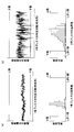
- the graphs in the lower diagram represent histograms that summarize the distribution of the number of pixels (area) in the black portion in the upper diagram.
- the horizontal axis indicates the number of black pixels (area)
- the vertical axis indicates the frequency of occurrence.
- the pressurizing unit 32 is set with the same pressurizing force due to changes in weather between morning and night, the actual pressurizing force deviates from the set value. For example, when pressed shallowly, the pattern is thin and the area occupied by the pattern is small. On the other hand, when pressed deeply, the pattern is dark and the area occupied by the pattern becomes large. In this way, adjustment is made by looking at the result of the area of the pattern that changes with time and weather.
- the depth of the pattern recess depends on the hardness of the gypsum board to be processed, but the hardness of the gypsum board itself depends on several factors such as the gypsum raw material, how to mix water and calcined gypsum, and drying conditions. There are factors, and complex calculations are required to make adjustments. Therefore, the variation in the pattern is more directly solved by adjusting the press device 30 that performs patterning.
- the area occupied by the pattern calculated in the inspection process is fed back, and the pressing amount or the pressing time of the press devices 30 ⁇ and 30 ⁇ is adjusted in the processing process, whereby the uneven board Variation in the depth of the hole-like depression for each B2 can be reduced.
- the uneven board B2 formed with unevenness has, for example, a large area of a 1.5 ⁇ 3.0 pressurizing portion, so that the pressure may vary even within a single board.
- the pattern is determined by dividing the inside of one board, the variation in one board can be adjusted.
- the variation in one board can be adjusted. it can.
- FIG. 17 shows the inspection results before and after adjusting the pattern variation by the two press devices 30.
- FIG. 17A is a graph obtained by superimposing histogram outlines of the No. 1 press and the No. 2 press shown in FIG. 16B.
- FIG. 17B is a graph obtained by superimposing histogram outlines for the No. 1 press and the No. 2 press after adjusting the pattern variation between the No. 1 press and the No. 2 press.
- the patterns formed by the two press devices 30 ⁇ and 30 ⁇ are inspected by calculating the pattern ratios in the inspection process. Then, according to the result, the press amount is adjusted so that the pattern formed by the first press apparatus 30 ⁇ ) and the pattern formed by the second press apparatus 30 ⁇ ) are made uniform. Thereby, even if products using two types of press devices are mixed in the manufacturing process, variation in the darkness of the pattern can be suppressed.
- a travertine pattern in which a number of fine hole-like depressions are formed on the surface of a white or high-lightness color is described as a pattern of a board with a pattern that is an inspection object.
- the pattern of the inspection object used in the inspection method of the present invention is not limited to the travertine pattern.
- the pattern may be a grain pattern formed by laminating a decorative layer, such as a sheet on which a grain pattern is formed.
- a defective product may occur due to misalignment of the base material and the sheet due to a defect in the lamination means or the like.
- comparing and comparing a reference image serving as a comparison reference for inspection and an image created in the numerical process it is possible to distinguish a pattern from a defect on a surface to be inspected of a patterned board that is an inspection object. It can be determined whether or not there is.
- the size of the pattern does not change so much, but the position of the pattern may be shifted depending on how the sheet is attached to the plate-like member. Therefore, it is possible to determine whether there is a pattern shift by comparing with a reference image as a pattern inspection.
- the board pattern used in the present embodiment is a wood grain
- the wood grain pattern is stored, a threshold value is provided for the wood part in the orange constituting the wood, and the color is separated and extracted (2 An image to be compared with a reference image may be created.
- the inspection result by the inspection apparatus may be notified in a subsequent process as shown in FIG.
- various apparatuses may be adjusted so that the inspection result based on the inspection result is fed back and the content of the defect is corrected ( An adjustment device may be provided).
- the position where the resin sheet is attached to the plate-like member is adjusted according to the inspection result of the pattern in the inspection process. Therefore, a machine can be returned to a favorable state and manufacturing variation can be reduced.
- the pattern of the board with a pattern that is an inspection object is an example of a travertine pattern
- the pattern of the inspection object is an example of a wood grain pattern.
- the patterns that can be inspected by the inspection apparatus of the present invention may be further printed on these patterns.
- a logo or the like may be printed on the gypsum board in order to indicate the manufacturer or the store name.
- the pattern of the pattern is stored, the pattern of the print is further stored, and the entire image is binarized, or the pattern portion is binarized with respect to the background without the pattern, the binarization of the print portion,
- the inspection image for comparison with the reference image may be created by separately performing the above.
- the gypsum board which is the inspection object of the first, second, and fourth embodiments of the present invention, is, for example, bonded to calcined gypsum (CaSO 4 ⁇ 1 / 2H 2 O) with a setting adjuster or a base paper for board. It is molded by blending with a property improver and kneading with water. Various additives such as reinforcing fibers and lightweight aggregates, refractory materials, setting modifiers, water reducing agents, foams, foam diameter adjusting agents and the like may be blended as necessary.
- the gypsum board which is an inspection object used in the third and fourth embodiments of the present invention, is formed into a plate shape by covering gypsum as a core material on one or both sides with a base paper for gypsum board.
- the present invention has been described based on each embodiment, but the present invention is not limited to the requirements shown in the above embodiment. With respect to these points, the gist of the present invention can be changed without departing from the scope of the present invention, and can be appropriately determined according to the application form.
Landscapes
- Engineering & Computer Science (AREA)
- Textile Engineering (AREA)
- Life Sciences & Earth Sciences (AREA)
- Physics & Mathematics (AREA)
- General Physics & Mathematics (AREA)
- General Health & Medical Sciences (AREA)
- Pathology (AREA)
- Immunology (AREA)
- Health & Medical Sciences (AREA)
- Chemical & Material Sciences (AREA)
- Analytical Chemistry (AREA)
- Biochemistry (AREA)
- Wood Science & Technology (AREA)
- Theoretical Computer Science (AREA)
- Computer Vision & Pattern Recognition (AREA)
- Quality & Reliability (AREA)
- Investigating Materials By The Use Of Optical Means Adapted For Particular Applications (AREA)
- Image Processing (AREA)
- Testing Or Measuring Of Semiconductors Or The Like (AREA)
- Image Analysis (AREA)
- Length Measuring Devices By Optical Means (AREA)
Abstract
Priority Applications (12)
| Application Number | Priority Date | Filing Date | Title |
|---|---|---|---|
| AU2017296488A AU2017296488B2 (en) | 2016-07-12 | 2017-06-16 | Inspection method, inspection/notification method, manufacturing method including inspection method, inspection apparatus, and manufacturing apparatus |
| MYPI2018003022A MY193069A (en) | 2016-07-12 | 2017-06-16 | Inspection method, inspection and reporting method, manufacturing method including the inspection method, inspection apparatus, and manufacturing apparatus |
| PL17827323.1T PL3486638T3 (pl) | 2016-07-12 | 2017-06-16 | Sposób kontroli, sposób kontroli i raportowania, sposób wytwarzania, w tym sposób kontroli, urządzenie kontrolujące i urządzenie wytwarzające |
| US16/316,168 US10830707B2 (en) | 2016-07-12 | 2017-06-16 | Inspection method, inspection and reporting method, manufacturing method including the inspection method, inspection apparatus, and manufacturing apparatus |
| ES17827323T ES2965966T3 (es) | 2016-07-12 | 2017-06-16 | Método de inspección, método de inspección y notificación, método de fabricación que incluye el método de inspección, aparato de inspección y aparato de fabricación |
| JP2018527461A JP6997457B2 (ja) | 2016-07-12 | 2017-06-16 | 検査方法、検査・通知方法、該検査方法を含む製造方法、検査装置及び製造装置 |
| EP17827323.1A EP3486638B1 (fr) | 2016-07-12 | 2017-06-16 | Procédé d'inspection, procédé d'inspection et de notification, procédé de fabrication comprenant le procédé d'inspection, appareil d'inspection et appareil de fabrication |
| KR1020187038091A KR102270741B1 (ko) | 2016-07-12 | 2017-06-16 | 검사 방법, 검사·통지 방법, 당해 검사 방법을 포함하는 제조 방법, 검사 장치 및 제조 장치 |
| MX2018015199A MX2018015199A (es) | 2016-07-12 | 2017-06-16 | Metodo de inspeccion, metodo de inspeccion y notificacion, metodo de fabricacion que incluye el metodo de inspeccion, aparato de inspeccion y aparato de fabricacion. |
| RU2018147223A RU2727913C1 (ru) | 2016-07-12 | 2017-06-16 | Способ контроля, способ контроля и передачи информации, способ изготовления, включающий способ контроля, устройство контроля и производственная установка |
| CN201780041407.0A CN109477803B (zh) | 2016-07-12 | 2017-06-16 | 检查方法、检查·通知方法、包括该检查方法的制造方法、检查装置及制造装置 |
| CA3029218A CA3029218C (fr) | 2016-07-12 | 2017-06-16 | Procede d'inspection, procede d'inspection/notification, procede de fabrication comprenant le procede d'inspection, appareil d'inspection et appareil de fabrication |
Applications Claiming Priority (2)
| Application Number | Priority Date | Filing Date | Title |
|---|---|---|---|
| JP2016137994 | 2016-07-12 | ||
| JP2016-137994 | 2016-07-12 |
Publications (1)
| Publication Number | Publication Date |
|---|---|
| WO2018012192A1 true WO2018012192A1 (fr) | 2018-01-18 |
Family
ID=60952555
Family Applications (1)
| Application Number | Title | Priority Date | Filing Date |
|---|---|---|---|
| PCT/JP2017/022279 WO2018012192A1 (fr) | 2016-07-12 | 2017-06-16 | Procédé d'inspection, procédé d'inspection/notification, procédé de fabrication comprenant le procédé d'inspection, appareil d'inspection et appareil de fabrication |
Country Status (13)
| Country | Link |
|---|---|
| US (1) | US10830707B2 (fr) |
| EP (1) | EP3486638B1 (fr) |
| JP (1) | JP6997457B2 (fr) |
| KR (1) | KR102270741B1 (fr) |
| CN (1) | CN109477803B (fr) |
| AU (1) | AU2017296488B2 (fr) |
| CA (1) | CA3029218C (fr) |
| ES (1) | ES2965966T3 (fr) |
| MX (1) | MX2018015199A (fr) |
| MY (1) | MY193069A (fr) |
| PL (1) | PL3486638T3 (fr) |
| RU (1) | RU2727913C1 (fr) |
| WO (1) | WO2018012192A1 (fr) |
Cited By (4)
| Publication number | Priority date | Publication date | Assignee | Title |
|---|---|---|---|---|
| JP2020092855A (ja) * | 2018-12-13 | 2020-06-18 | 三菱電機株式会社 | 縫製制御装置、縫製制御システム、縫製制御方法およびプログラム |
| US20220099589A1 (en) * | 2019-02-28 | 2022-03-31 | Yoshino Gypsum Co., Ltd. | Apparatus for inspecting plate-like bodies |
| JP7274026B1 (ja) | 2022-07-05 | 2023-05-15 | 株式会社ジーテクト | プレス機 |
| CN116213271A (zh) * | 2023-04-28 | 2023-06-06 | 山东瑞邦智能装备股份有限公司 | 装饰石膏板自动缺陷检测与智能剔除装置及其工作方法 |
Families Citing this family (6)
| Publication number | Priority date | Publication date | Assignee | Title |
|---|---|---|---|---|
| CN107067421B (zh) * | 2017-05-12 | 2020-02-28 | 京东方科技集团股份有限公司 | 一种基板残材检测方法、装置及系统 |
| US11878873B2 (en) * | 2021-01-19 | 2024-01-23 | Symbotic Canada, Ulc | Cased goods inspection and method therefor |
| WO2022157763A1 (fr) * | 2021-01-25 | 2022-07-28 | Inspect Technologies Ltd | Inspection de grains automatisée |
| CN114913108A (zh) * | 2021-01-29 | 2022-08-16 | 京东方科技集团股份有限公司 | 显示基板的图像分类方法和装置 |
| RU2768691C1 (ru) * | 2021-08-16 | 2022-03-24 | федеральное государственное бюджетное образовательное учреждение высшего образования "Марийский государственный университет" | Способ получения профиля вдоль линии сканирования и профиля поверхности по изображению, полученному с цифрового устройства |
| WO2024084305A1 (fr) * | 2022-10-17 | 2024-04-25 | Georgia-Pacific Gypsum Llc | Système, appareil et procédés d'inspection de déchirure |
Citations (12)
| Publication number | Priority date | Publication date | Assignee | Title |
|---|---|---|---|---|
| JPS5870150A (ja) * | 1981-10-22 | 1983-04-26 | Fuji Electric Co Ltd | 光学検査装置用照明器 |
| JPS60227107A (ja) * | 1984-04-25 | 1985-11-12 | Matsushita Electric Works Ltd | 欠点検出装置 |
| JPS6375507A (ja) * | 1986-09-19 | 1988-04-05 | Toshiba Corp | くぼみ穴測定方法及び装置 |
| JPH06147855A (ja) * | 1992-11-10 | 1994-05-27 | Hiyuu Burein:Kk | 画像検査方法 |
| JP2002181718A (ja) * | 2000-12-14 | 2002-06-26 | Dainippon Printing Co Ltd | ホログラムシートの検査方法及び検査装置 |
| JP2004334491A (ja) * | 2003-05-07 | 2004-11-25 | Seiko Epson Corp | 貼付位置画像検査装置、貼付位置画像検査方法、電気光学装置モジュールの製造装置、電気光学装置モジュールの製造方法、電子部品付き回路基板の製造装置及び電子部品付き回路基板の製造方法 |
| JP2005164309A (ja) * | 2003-12-01 | 2005-06-23 | Hitachi Kokusai Electric Inc | 目視検査装置 |
| JP2007248376A (ja) * | 2006-03-17 | 2007-09-27 | National Printing Bureau | Ovd箔上の印刷模様の検査方法及び検査装置 |
| US20080030745A1 (en) * | 2006-08-05 | 2008-02-07 | Uhlmann Pac-Systeme Gmbh & Co. Kg | Quality-control method for laminated-foil packaging system |
| JP2008155345A (ja) * | 2006-12-26 | 2008-07-10 | Hitachi-Ge Nuclear Energy Ltd | ウォータージェットピーニング施工面の残留応力評価方法 |
| JP2010139461A (ja) * | 2008-12-15 | 2010-06-24 | Toppan Printing Co Ltd | 目視検査システム |
| JP2014219256A (ja) * | 2013-05-08 | 2014-11-20 | ケイミュー株式会社 | 柄計測方法 |
Family Cites Families (22)
| Publication number | Priority date | Publication date | Assignee | Title |
|---|---|---|---|---|
| JPH01297542A (ja) * | 1988-05-25 | 1989-11-30 | Csk Corp | 欠陥検査装置 |
| WO1998059213A1 (fr) * | 1997-06-25 | 1998-12-30 | Matsushita Electric Works, Ltd. | Procede et dispositif de controle de motifs |
| JP4293653B2 (ja) | 1998-10-23 | 2009-07-08 | パナソニック電工株式会社 | 外観検査方法 |
| JP4548912B2 (ja) * | 2000-08-11 | 2010-09-22 | パナソニック株式会社 | 透明液体検査装置、および透明液体塗布装置、および透明液体検査方法、および透明液体塗布方法 |
| JP4038356B2 (ja) * | 2001-04-10 | 2008-01-23 | 株式会社日立製作所 | 欠陥データ解析方法及びその装置並びにレビューシステム |
| JP3698075B2 (ja) * | 2001-06-20 | 2005-09-21 | 株式会社日立製作所 | 半導体基板の検査方法およびその装置 |
| JP3914530B2 (ja) * | 2003-10-16 | 2007-05-16 | 株式会社日立製作所 | 欠陥検査装置 |
| JP4776197B2 (ja) * | 2004-09-21 | 2011-09-21 | 日本特殊陶業株式会社 | 配線基板の検査装置 |
| JP2007240432A (ja) * | 2006-03-10 | 2007-09-20 | Omron Corp | 欠陥検査装置および欠陥検査方法 |
| KR20090024943A (ko) * | 2007-09-05 | 2009-03-10 | 아주하이텍(주) | 자동 광학 검사 장치 및 방법 |
| JPWO2011004534A1 (ja) | 2009-07-09 | 2012-12-13 | 株式会社日立ハイテクノロジーズ | 半導体欠陥分類方法,半導体欠陥分類装置,半導体欠陥分類プログラム |
| KR101214806B1 (ko) * | 2010-05-11 | 2012-12-24 | 가부시키가이샤 사무코 | 웨이퍼 결함 검사 장치 및 웨이퍼 결함 검사 방법 |
| JP4700141B1 (ja) * | 2010-09-17 | 2011-06-15 | 東洋ガラス株式会社 | ガラス製品のゴブ検査装置 |
| JP2012088199A (ja) * | 2010-10-20 | 2012-05-10 | Yamaha Motor Co Ltd | 異物検査装置および異物検査方法 |
| JP2012242268A (ja) * | 2011-05-20 | 2012-12-10 | Toppan Printing Co Ltd | 検査装置及び検査方法 |
| CN102507597B (zh) * | 2011-10-08 | 2014-04-23 | 苏州赛琅泰克高技术陶瓷有限公司 | 陶瓷基板镭射孔洞检测系统及其检测方法 |
| JP2013157369A (ja) * | 2012-01-27 | 2013-08-15 | Dainippon Screen Mfg Co Ltd | ステージ移動装置 |
| CN102879402B (zh) * | 2012-10-10 | 2015-01-14 | 北新集团建材股份有限公司 | 板材缺陷的影像检测控制方法 |
| CA2887555C (fr) * | 2012-10-18 | 2019-12-31 | Yoshino Gypsum Co., Ltd. | Procede de detection de vides dans un panneau de construction a base de gypse et procede de production de panneau de construction a base de gypse |
| JP2015197396A (ja) * | 2014-04-02 | 2015-11-09 | 三菱電機株式会社 | 画像検査方法および画像検査装置 |
| JP6499898B2 (ja) * | 2014-05-14 | 2019-04-10 | 株式会社ニューフレアテクノロジー | 検査方法、テンプレート基板およびフォーカスオフセット方法 |
| KR101730787B1 (ko) * | 2014-07-08 | 2017-04-27 | 닛산 지도우샤 가부시키가이샤 | 결함 검사 장치 및 생산 시스템 |
-
2017
- 2017-06-16 KR KR1020187038091A patent/KR102270741B1/ko active IP Right Grant
- 2017-06-16 CN CN201780041407.0A patent/CN109477803B/zh active Active
- 2017-06-16 PL PL17827323.1T patent/PL3486638T3/pl unknown
- 2017-06-16 RU RU2018147223A patent/RU2727913C1/ru active
- 2017-06-16 JP JP2018527461A patent/JP6997457B2/ja active Active
- 2017-06-16 MY MYPI2018003022A patent/MY193069A/en unknown
- 2017-06-16 ES ES17827323T patent/ES2965966T3/es active Active
- 2017-06-16 AU AU2017296488A patent/AU2017296488B2/en active Active
- 2017-06-16 WO PCT/JP2017/022279 patent/WO2018012192A1/fr active Search and Examination
- 2017-06-16 CA CA3029218A patent/CA3029218C/fr active Active
- 2017-06-16 MX MX2018015199A patent/MX2018015199A/es unknown
- 2017-06-16 US US16/316,168 patent/US10830707B2/en active Active
- 2017-06-16 EP EP17827323.1A patent/EP3486638B1/fr active Active
Patent Citations (12)
| Publication number | Priority date | Publication date | Assignee | Title |
|---|---|---|---|---|
| JPS5870150A (ja) * | 1981-10-22 | 1983-04-26 | Fuji Electric Co Ltd | 光学検査装置用照明器 |
| JPS60227107A (ja) * | 1984-04-25 | 1985-11-12 | Matsushita Electric Works Ltd | 欠点検出装置 |
| JPS6375507A (ja) * | 1986-09-19 | 1988-04-05 | Toshiba Corp | くぼみ穴測定方法及び装置 |
| JPH06147855A (ja) * | 1992-11-10 | 1994-05-27 | Hiyuu Burein:Kk | 画像検査方法 |
| JP2002181718A (ja) * | 2000-12-14 | 2002-06-26 | Dainippon Printing Co Ltd | ホログラムシートの検査方法及び検査装置 |
| JP2004334491A (ja) * | 2003-05-07 | 2004-11-25 | Seiko Epson Corp | 貼付位置画像検査装置、貼付位置画像検査方法、電気光学装置モジュールの製造装置、電気光学装置モジュールの製造方法、電子部品付き回路基板の製造装置及び電子部品付き回路基板の製造方法 |
| JP2005164309A (ja) * | 2003-12-01 | 2005-06-23 | Hitachi Kokusai Electric Inc | 目視検査装置 |
| JP2007248376A (ja) * | 2006-03-17 | 2007-09-27 | National Printing Bureau | Ovd箔上の印刷模様の検査方法及び検査装置 |
| US20080030745A1 (en) * | 2006-08-05 | 2008-02-07 | Uhlmann Pac-Systeme Gmbh & Co. Kg | Quality-control method for laminated-foil packaging system |
| JP2008155345A (ja) * | 2006-12-26 | 2008-07-10 | Hitachi-Ge Nuclear Energy Ltd | ウォータージェットピーニング施工面の残留応力評価方法 |
| JP2010139461A (ja) * | 2008-12-15 | 2010-06-24 | Toppan Printing Co Ltd | 目視検査システム |
| JP2014219256A (ja) * | 2013-05-08 | 2014-11-20 | ケイミュー株式会社 | 柄計測方法 |
Cited By (7)
| Publication number | Priority date | Publication date | Assignee | Title |
|---|---|---|---|---|
| JP2020092855A (ja) * | 2018-12-13 | 2020-06-18 | 三菱電機株式会社 | 縫製制御装置、縫製制御システム、縫製制御方法およびプログラム |
| US20220099589A1 (en) * | 2019-02-28 | 2022-03-31 | Yoshino Gypsum Co., Ltd. | Apparatus for inspecting plate-like bodies |
| US11692944B2 (en) * | 2019-02-28 | 2023-07-04 | Yoshino Gypsum Co., Ltd. | Apparatus for inspecting plate-like bodies |
| JP7274026B1 (ja) | 2022-07-05 | 2023-05-15 | 株式会社ジーテクト | プレス機 |
| JP2024007188A (ja) * | 2022-07-05 | 2024-01-18 | 株式会社ジーテクト | プレス機 |
| CN116213271A (zh) * | 2023-04-28 | 2023-06-06 | 山东瑞邦智能装备股份有限公司 | 装饰石膏板自动缺陷检测与智能剔除装置及其工作方法 |
| CN116213271B (zh) * | 2023-04-28 | 2023-08-11 | 山东瑞邦智能装备股份有限公司 | 装饰石膏板自动缺陷检测与智能剔除装置及其工作方法 |
Also Published As
| Publication number | Publication date |
|---|---|
| RU2727913C1 (ru) | 2020-07-24 |
| PL3486638T3 (pl) | 2024-03-04 |
| EP3486638B1 (fr) | 2023-09-20 |
| EP3486638A1 (fr) | 2019-05-22 |
| AU2017296488A1 (en) | 2019-01-24 |
| MX2018015199A (es) | 2019-04-22 |
| KR102270741B1 (ko) | 2021-06-28 |
| CA3029218A1 (fr) | 2018-01-18 |
| EP3486638A4 (fr) | 2019-09-11 |
| ES2965966T3 (es) | 2024-04-17 |
| US10830707B2 (en) | 2020-11-10 |
| MY193069A (en) | 2022-09-26 |
| JPWO2018012192A1 (ja) | 2019-04-25 |
| CA3029218C (fr) | 2024-02-20 |
| CN109477803A (zh) | 2019-03-15 |
| KR20190028391A (ko) | 2019-03-18 |
| AU2017296488B2 (en) | 2021-10-28 |
| JP6997457B2 (ja) | 2022-01-20 |
| US20200124541A1 (en) | 2020-04-23 |
| CN109477803B (zh) | 2022-04-26 |
Similar Documents
| Publication | Publication Date | Title |
|---|---|---|
| WO2018012192A1 (fr) | Procédé d'inspection, procédé d'inspection/notification, procédé de fabrication comprenant le procédé d'inspection, appareil d'inspection et appareil de fabrication | |
| US9839946B2 (en) | System and method for high speed FOD detection | |
| JP2006300663A (ja) | 欠点検出システム | |
| JP4589101B2 (ja) | 表面検査方法および同装置 | |
| US20190039314A1 (en) | Three-Dimensional Shaping Method | |
| JP2007298472A (ja) | ケースの検査装置および検査方法 | |
| JP2005257681A (ja) | 表面検査方法および同装置 | |
| JP2007033295A (ja) | 検査装置 | |
| JP5902067B2 (ja) | 紙粉の付着量検査方法および紙粉付着量検査装置 | |
| JP2020034345A (ja) | 検査システム、検査方法 | |
| JP4563184B2 (ja) | ムラ欠陥の検査方法および装置 | |
| JP6428554B2 (ja) | 検査システム、検査方法 | |
| JP2014038013A (ja) | 平判紙の積層状態不良検知方法および平判紙積層状態不良検知装置 | |
| JP2002365227A (ja) | プレス品の検査装置 | |
| JP4444048B2 (ja) | 熱可塑性接着剤検査装置及び検査方法 | |
| TW202033930A (zh) | 吸煙物品用包裝容器的檢查裝置、製造裝置及檢查方法 | |
| JP2006189293A (ja) | スジ状ムラ欠陥の検査方法および装置 | |
| JP4779790B2 (ja) | ガラス板面の識別方法およびその装置 | |
| JP2005153928A (ja) | 検査機能付きトレー供給装置及びトレー供給移載装置 | |
| JP2019155625A (ja) | 成形品の撮影方法および成形品の撮影装置 | |
| JP2013134136A (ja) | 表面欠陥検査システム | |
| JP2011102765A (ja) | 撮像方法、画像処理方法および撮像・画像処理装置 | |
| JP2000283740A (ja) | 押出成形品の外観検査装置 | |
| JP2021135062A (ja) | 複合シートの製造方法及び製造装置 | |
| JP2814183B2 (ja) | 画像処理装置における撮像装置選定方法 |
Legal Events
| Date | Code | Title | Description |
|---|---|---|---|
| DPE1 | Request for preliminary examination filed after expiration of 19th month from priority date (pct application filed from 20040101) | ||
| 121 | Ep: the epo has been informed by wipo that ep was designated in this application |
Ref document number: 17827323 Country of ref document: EP Kind code of ref document: A1 |
|
| ENP | Entry into the national phase |
Ref document number: 3029218 Country of ref document: CA |
|
| ENP | Entry into the national phase |
Ref document number: 20187038091 Country of ref document: KR Kind code of ref document: A |
|
| ENP | Entry into the national phase |
Ref document number: 2018527461 Country of ref document: JP Kind code of ref document: A |
|
| NENP | Non-entry into the national phase |
Ref country code: DE |
|
| ENP | Entry into the national phase |
Ref document number: 2017296488 Country of ref document: AU Date of ref document: 20170616 Kind code of ref document: A |
|
| ENP | Entry into the national phase |
Ref document number: 2017827323 Country of ref document: EP Effective date: 20190212 |