WO2018003229A1 - 電子写真用感光体およびそれを搭載した電子写真装置 - Google Patents
電子写真用感光体およびそれを搭載した電子写真装置 Download PDFInfo
- Publication number
- WO2018003229A1 WO2018003229A1 PCT/JP2017/014684 JP2017014684W WO2018003229A1 WO 2018003229 A1 WO2018003229 A1 WO 2018003229A1 JP 2017014684 W JP2017014684 W JP 2017014684W WO 2018003229 A1 WO2018003229 A1 WO 2018003229A1
- Authority
- WO
- WIPO (PCT)
- Prior art keywords
- charge transport
- silane coupling
- coupling agent
- photoreceptor
- layer
- Prior art date
- Legal status (The legal status is an assumption and is not a legal conclusion. Google has not performed a legal analysis and makes no representation as to the accuracy of the status listed.)
- Ceased
Links
Images

Classifications
-
- G—PHYSICS
- G03—PHOTOGRAPHY; CINEMATOGRAPHY; ANALOGOUS TECHNIQUES USING WAVES OTHER THAN OPTICAL WAVES; ELECTROGRAPHY; HOLOGRAPHY
- G03G—ELECTROGRAPHY; ELECTROPHOTOGRAPHY; MAGNETOGRAPHY
- G03G5/00—Recording-members for original recording by exposure, e.g. to light, to heat or to electrons; Manufacture thereof; Selection of materials therefor
- G03G5/02—Charge-receiving layers
- G03G5/04—Photoconductive layers; Charge-generation layers or charge-transporting layers; Additives therefor; Binders therefor
- G03G5/05—Organic bonding materials; Methods for coating a substrate with a photoconductive layer; Inert supplements for use in photoconductive layers
- G03G5/0503—Inert supplements
- G03G5/0507—Inorganic compounds
-
- G—PHYSICS
- G03—PHOTOGRAPHY; CINEMATOGRAPHY; ANALOGOUS TECHNIQUES USING WAVES OTHER THAN OPTICAL WAVES; ELECTROGRAPHY; HOLOGRAPHY
- G03G—ELECTROGRAPHY; ELECTROPHOTOGRAPHY; MAGNETOGRAPHY
- G03G5/00—Recording-members for original recording by exposure, e.g. to light, to heat or to electrons; Manufacture thereof; Selection of materials therefor
- G03G5/02—Charge-receiving layers
- G03G5/04—Photoconductive layers; Charge-generation layers or charge-transporting layers; Additives therefor; Binders therefor
- G03G5/05—Organic bonding materials; Methods for coating a substrate with a photoconductive layer; Inert supplements for use in photoconductive layers
-
- G—PHYSICS
- G03—PHOTOGRAPHY; CINEMATOGRAPHY; ANALOGOUS TECHNIQUES USING WAVES OTHER THAN OPTICAL WAVES; ELECTROGRAPHY; HOLOGRAPHY
- G03G—ELECTROGRAPHY; ELECTROPHOTOGRAPHY; MAGNETOGRAPHY
- G03G5/00—Recording-members for original recording by exposure, e.g. to light, to heat or to electrons; Manufacture thereof; Selection of materials therefor
- G03G5/02—Charge-receiving layers
- G03G5/04—Photoconductive layers; Charge-generation layers or charge-transporting layers; Additives therefor; Binders therefor
- G03G5/043—Photoconductive layers characterised by having two or more layers or characterised by their composite structure
- G03G5/047—Photoconductive layers characterised by having two or more layers or characterised by their composite structure characterised by the charge-generation layers or charge transport layers
-
- G—PHYSICS
- G03—PHOTOGRAPHY; CINEMATOGRAPHY; ANALOGOUS TECHNIQUES USING WAVES OTHER THAN OPTICAL WAVES; ELECTROGRAPHY; HOLOGRAPHY
- G03G—ELECTROGRAPHY; ELECTROPHOTOGRAPHY; MAGNETOGRAPHY
- G03G5/00—Recording-members for original recording by exposure, e.g. to light, to heat or to electrons; Manufacture thereof; Selection of materials therefor
- G03G5/02—Charge-receiving layers
- G03G5/04—Photoconductive layers; Charge-generation layers or charge-transporting layers; Additives therefor; Binders therefor
- G03G5/05—Organic bonding materials; Methods for coating a substrate with a photoconductive layer; Inert supplements for use in photoconductive layers
- G03G5/0525—Coating methods
-
- G—PHYSICS
- G03—PHOTOGRAPHY; CINEMATOGRAPHY; ANALOGOUS TECHNIQUES USING WAVES OTHER THAN OPTICAL WAVES; ELECTROGRAPHY; HOLOGRAPHY
- G03G—ELECTROGRAPHY; ELECTROPHOTOGRAPHY; MAGNETOGRAPHY
- G03G5/00—Recording-members for original recording by exposure, e.g. to light, to heat or to electrons; Manufacture thereof; Selection of materials therefor
- G03G5/02—Charge-receiving layers
- G03G5/04—Photoconductive layers; Charge-generation layers or charge-transporting layers; Additives therefor; Binders therefor
- G03G5/05—Organic bonding materials; Methods for coating a substrate with a photoconductive layer; Inert supplements for use in photoconductive layers
- G03G5/0528—Macromolecular bonding materials
- G03G5/0532—Macromolecular bonding materials obtained by reactions only involving carbon-to-carbon unsatured bonds
- G03G5/0546—Polymers comprising at least one carboxyl radical, e.g. polyacrylic acid, polycrotonic acid, polymaleic acid; Derivatives thereof, e.g. their esters, salts, anhydrides, nitriles, amides
-
- G—PHYSICS
- G03—PHOTOGRAPHY; CINEMATOGRAPHY; ANALOGOUS TECHNIQUES USING WAVES OTHER THAN OPTICAL WAVES; ELECTROGRAPHY; HOLOGRAPHY
- G03G—ELECTROGRAPHY; ELECTROPHOTOGRAPHY; MAGNETOGRAPHY
- G03G5/00—Recording-members for original recording by exposure, e.g. to light, to heat or to electrons; Manufacture thereof; Selection of materials therefor
- G03G5/02—Charge-receiving layers
- G03G5/04—Photoconductive layers; Charge-generation layers or charge-transporting layers; Additives therefor; Binders therefor
- G03G5/05—Organic bonding materials; Methods for coating a substrate with a photoconductive layer; Inert supplements for use in photoconductive layers
- G03G5/0528—Macromolecular bonding materials
- G03G5/0557—Macromolecular bonding materials obtained otherwise than by reactions only involving carbon-to-carbon unsatured bonds
- G03G5/0564—Polycarbonates
-
- G—PHYSICS
- G03—PHOTOGRAPHY; CINEMATOGRAPHY; ANALOGOUS TECHNIQUES USING WAVES OTHER THAN OPTICAL WAVES; ELECTROGRAPHY; HOLOGRAPHY
- G03G—ELECTROGRAPHY; ELECTROPHOTOGRAPHY; MAGNETOGRAPHY
- G03G5/00—Recording-members for original recording by exposure, e.g. to light, to heat or to electrons; Manufacture thereof; Selection of materials therefor
- G03G5/02—Charge-receiving layers
- G03G5/04—Photoconductive layers; Charge-generation layers or charge-transporting layers; Additives therefor; Binders therefor
- G03G5/06—Photoconductive layers; Charge-generation layers or charge-transporting layers; Additives therefor; Binders therefor characterised by the photoconductive material being organic
-
- G—PHYSICS
- G03—PHOTOGRAPHY; CINEMATOGRAPHY; ANALOGOUS TECHNIQUES USING WAVES OTHER THAN OPTICAL WAVES; ELECTROGRAPHY; HOLOGRAPHY
- G03G—ELECTROGRAPHY; ELECTROPHOTOGRAPHY; MAGNETOGRAPHY
- G03G5/00—Recording-members for original recording by exposure, e.g. to light, to heat or to electrons; Manufacture thereof; Selection of materials therefor
- G03G5/02—Charge-receiving layers
- G03G5/04—Photoconductive layers; Charge-generation layers or charge-transporting layers; Additives therefor; Binders therefor
- G03G5/06—Photoconductive layers; Charge-generation layers or charge-transporting layers; Additives therefor; Binders therefor characterised by the photoconductive material being organic
- G03G5/0601—Acyclic or carbocyclic compounds
- G03G5/0612—Acyclic or carbocyclic compounds containing nitrogen
- G03G5/0614—Amines
- G03G5/06142—Amines arylamine
- G03G5/06144—Amines arylamine diamine
- G03G5/061443—Amines arylamine diamine benzidine
-
- G—PHYSICS
- G03—PHOTOGRAPHY; CINEMATOGRAPHY; ANALOGOUS TECHNIQUES USING WAVES OTHER THAN OPTICAL WAVES; ELECTROGRAPHY; HOLOGRAPHY
- G03G—ELECTROGRAPHY; ELECTROPHOTOGRAPHY; MAGNETOGRAPHY
- G03G5/00—Recording-members for original recording by exposure, e.g. to light, to heat or to electrons; Manufacture thereof; Selection of materials therefor
- G03G5/02—Charge-receiving layers
- G03G5/04—Photoconductive layers; Charge-generation layers or charge-transporting layers; Additives therefor; Binders therefor
- G03G5/06—Photoconductive layers; Charge-generation layers or charge-transporting layers; Additives therefor; Binders therefor characterised by the photoconductive material being organic
- G03G5/0601—Acyclic or carbocyclic compounds
- G03G5/0612—Acyclic or carbocyclic compounds containing nitrogen
- G03G5/0614—Amines
- G03G5/06142—Amines arylamine
- G03G5/06147—Amines arylamine alkenylarylamine
- G03G5/061473—Amines arylamine alkenylarylamine plural alkenyl groups linked directly to the same aryl group
-
- G—PHYSICS
- G03—PHOTOGRAPHY; CINEMATOGRAPHY; ANALOGOUS TECHNIQUES USING WAVES OTHER THAN OPTICAL WAVES; ELECTROGRAPHY; HOLOGRAPHY
- G03G—ELECTROGRAPHY; ELECTROPHOTOGRAPHY; MAGNETOGRAPHY
- G03G5/00—Recording-members for original recording by exposure, e.g. to light, to heat or to electrons; Manufacture thereof; Selection of materials therefor
- G03G5/02—Charge-receiving layers
- G03G5/04—Photoconductive layers; Charge-generation layers or charge-transporting layers; Additives therefor; Binders therefor
- G03G5/06—Photoconductive layers; Charge-generation layers or charge-transporting layers; Additives therefor; Binders therefor characterised by the photoconductive material being organic
- G03G5/0622—Heterocyclic compounds
- G03G5/0624—Heterocyclic compounds containing one hetero ring
- G03G5/0627—Heterocyclic compounds containing one hetero ring being five-membered
- G03G5/0629—Heterocyclic compounds containing one hetero ring being five-membered containing one hetero atom
-
- G—PHYSICS
- G03—PHOTOGRAPHY; CINEMATOGRAPHY; ANALOGOUS TECHNIQUES USING WAVES OTHER THAN OPTICAL WAVES; ELECTROGRAPHY; HOLOGRAPHY
- G03G—ELECTROGRAPHY; ELECTROPHOTOGRAPHY; MAGNETOGRAPHY
- G03G5/00—Recording-members for original recording by exposure, e.g. to light, to heat or to electrons; Manufacture thereof; Selection of materials therefor
- G03G5/02—Charge-receiving layers
- G03G5/04—Photoconductive layers; Charge-generation layers or charge-transporting layers; Additives therefor; Binders therefor
- G03G5/06—Photoconductive layers; Charge-generation layers or charge-transporting layers; Additives therefor; Binders therefor characterised by the photoconductive material being organic
- G03G5/0664—Dyes
- G03G5/0696—Phthalocyanines
-
- G—PHYSICS
- G03—PHOTOGRAPHY; CINEMATOGRAPHY; ANALOGOUS TECHNIQUES USING WAVES OTHER THAN OPTICAL WAVES; ELECTROGRAPHY; HOLOGRAPHY
- G03G—ELECTROGRAPHY; ELECTROPHOTOGRAPHY; MAGNETOGRAPHY
- G03G5/00—Recording-members for original recording by exposure, e.g. to light, to heat or to electrons; Manufacture thereof; Selection of materials therefor
- G03G5/10—Bases for charge-receiving or other layers
- G03G5/102—Bases for charge-receiving or other layers consisting of or comprising metals
-
- G—PHYSICS
- G03—PHOTOGRAPHY; CINEMATOGRAPHY; ANALOGOUS TECHNIQUES USING WAVES OTHER THAN OPTICAL WAVES; ELECTROGRAPHY; HOLOGRAPHY
- G03G—ELECTROGRAPHY; ELECTROPHOTOGRAPHY; MAGNETOGRAPHY
- G03G5/00—Recording-members for original recording by exposure, e.g. to light, to heat or to electrons; Manufacture thereof; Selection of materials therefor
- G03G5/14—Inert intermediate or cover layers for charge-receiving layers
-
- G—PHYSICS
- G03—PHOTOGRAPHY; CINEMATOGRAPHY; ANALOGOUS TECHNIQUES USING WAVES OTHER THAN OPTICAL WAVES; ELECTROGRAPHY; HOLOGRAPHY
- G03G—ELECTROGRAPHY; ELECTROPHOTOGRAPHY; MAGNETOGRAPHY
- G03G5/00—Recording-members for original recording by exposure, e.g. to light, to heat or to electrons; Manufacture thereof; Selection of materials therefor
- G03G5/14—Inert intermediate or cover layers for charge-receiving layers
- G03G5/142—Inert intermediate layers
-
- G—PHYSICS
- G03—PHOTOGRAPHY; CINEMATOGRAPHY; ANALOGOUS TECHNIQUES USING WAVES OTHER THAN OPTICAL WAVES; ELECTROGRAPHY; HOLOGRAPHY
- G03G—ELECTROGRAPHY; ELECTROPHOTOGRAPHY; MAGNETOGRAPHY
- G03G2215/00—Apparatus for electrophotographic processes
- G03G2215/00953—Electrographic recording members
- G03G2215/00957—Compositions
Definitions
- the present invention relates to an electrophotographic photosensitive member (hereinafter also simply referred to as “photosensitive member”) used for an electrophotographic printer, copying machine, fax machine, and the like and an electrophotographic apparatus equipped with the photosensitive member.
- photosensitive member used for an electrophotographic printer, copying machine, fax machine, and the like
- electrophotographic apparatus equipped with the photosensitive member.
- the electrophotographic photoreceptor has a basic structure in which a photosensitive layer having a photoconductive function is provided on a conductive substrate.
- organic electrophotographic photoreceptors using organic compounds as functional components responsible for charge generation and transport have been actively researched and developed due to advantages such as material diversity, high productivity, and safety. Application to printers and printers is ongoing.
- a photoreceptor needs to have a function of holding a surface charge in a dark place, a function of receiving light to generate a charge, and a function of transporting the generated charge.
- So-called laminated type (functional separation type) photoreceptor comprising a photosensitive layer in which a functionally separated layer is laminated on a charge transporting layer, which has a function of retaining light and a function of transporting charges generated in the charge generation layer upon light reception There is.
- the photosensitive layer is generally formed by applying a coating solution in which a charge generating material, a charge transporting material and a resin binder are dissolved or dispersed in an organic solvent on a conductive substrate.
- a polycarbonate resin resin binder that is resistant to friction generated between paper and a blade for removing toner, has excellent flexibility, and has good exposure transparency. It is often used as.
- bisphenol Z-type polycarbonate is widely used as the resin binder.
- a technique using this polycarbonate as a resin binder is described in Patent Document 1 and the like.
- Methods for charging the photoconductor include a non-contact charging method in which the charging member such as scorotron is not in contact with the photoconductor, and contact in which the charging member made of a semiconductive rubber roller or brush contacts the photoconductor.
- a charging method There is a charging method.
- the contact charging method has the features that less corona discharge occurs in the vicinity of the photoreceptor than in the non-contact charging method, and therefore less ozone is generated and the applied voltage may be low. Therefore, since a more compact, low-cost, and low environmental pollution electrophotographic apparatus can be realized, it is mainly used for medium-sized to small-sized apparatuses.
- Patent Documents 2 and 3 propose a method of adding a filler to the surface layer of the photoreceptor in order to improve the durability of the photoreceptor surface.
- a filler to the surface layer of the photoreceptor in order to improve the durability of the photoreceptor surface.
- the aggregate of the filler exists, the transparency of the layer is reduced, or the exposure light is scattered by the filler, so that charge transport and charge generation become non-uniform and image characteristics are deteriorated.
- a dispersing agent in order to improve the dispersibility of the filler. In this case, since the dispersing agent itself affects the photoreceptor characteristics, it is possible to achieve both the dispersibility of the filler and the photoreceptor characteristics. It was difficult.
- Patent Documents 4 and 5 propose techniques for improving the filler content and dispersion state.
- the effects of these techniques are not sufficient, and development of an electrophotographic photoreceptor capable of achieving printing durability, repetitive stability, and high resolution is desired.
- Patent Document 6 contains inorganic particles having a number average primary particle size (Dp) of 5 to 100 nm, which has been subjected to surface treatment a plurality of times and surface treatment with silazane compounds as the last surface treatment, in the surface layer.
- An organic photoconductor is disclosed
- Patent Document 7 discloses an electrophotographic photoconductor in which a photosensitive layer on the outermost surface contains silica particles in a predetermined amount together with a predetermined functional material. .
- JP-A-61-62040 JP-A-1-205171 Japanese Patent Laid-Open No. 7-333881 JP-A-8-305051 JP 2006-201744 A JP 2006-301247 A JP2015-175948A
- an object of the present invention is to solve the above-mentioned problems, reduce the amount of wear on the surface of the photoconductor, and obtain a good image stably over a long period of time, and an electrophotographic apparatus equipped with the photoconductor. Is to provide.
- the present inventors have formulated a combination of a charge transporting material, a resin binder, and a silane coupling surface treatment filler with good compatibility in the layer that becomes the surface of the photoreceptor. As a result, it was found that the filler can be uniformly dispersed in the layer and a highly durable electrophotographic photoreceptor can be realized, and the present invention has been completed.
- a conductive substrate In an electrophotographic photoreceptor comprising a charge transport layer provided on the conductive substrate,
- the charge transport layer contains a charge transport material, a resin binder, and an inorganic oxide filler surface-treated with a silane coupling agent,
- the difference ⁇ SPa in the dipole force term of the Hansen solubility parameter between the charge transport material and the silane coupling agent satisfies the relationship ⁇ SPa ⁇ 1.0
- the difference ⁇ SPb in the London dispersion force term of the Hansen solubility parameter between the resin binder and the silane coupling agent satisfies the relationship ⁇ SPb ⁇ 2.5.
- Hansen solubility parameter is calculated using Hansen's equation that can divide the interaction of intermolecular forces into London dispersion force terms, dipole force terms, and hydrogen bond force terms. Is done.
- the London dispersion force term ⁇ d of the Hansen solubility parameter is calculated by the following equation.
- ⁇ d ⁇ Fd / V (J 1/2 / cm 3/2 ) (Where Fd is the Kreveren and Hoftizer parameter cohesive energy related to the London dispersion of each component, and V is the molar volume of each component)
- SPa the dipole force term of the Hansen solubility parameter
- SPb the London dispersion force term
- the inventors have determined the correlation between the terms of the Hansen solubility parameter and the compatibility between the charge transport material and the silane coupling agent, and the compatibility between the resin binder and the silane coupling agent.
- the former showed a high correlation with the difference between the dipole force terms and the latter with the difference in the London dispersion force term.
- the charge transport material and the resin binder are confirmed to have good compatibility in the range of materials usually used in the field of photoreceptors. Therefore, in the present invention, the charge transport material and the silane coupling are used. And the compatibility between the resin agent and between the resin binder and the silane coupling agent.
- the difference ⁇ SPa between the dipole force terms of the Hansen solubility parameter between the charge transport material and the silane coupling agent satisfies the relationship of ⁇ SPa ⁇ 1.0
- the resin By using a composition in which the difference ⁇ SPb in the London dispersion force term of the Hansen solubility parameter between the binder and the silane coupling agent satisfies the relationship of ⁇ SPb ⁇ 2.5 for the charge transport layer of the photoreceptor, good printing durability Can be obtained.
- the resin binder is preferably a polycarbonate resin or a polyarylate resin.
- the inorganic oxide filler preferably has a primary particle size of 1 to 200 nm.
- the charge transport material is preferably a hole transport material.
- the photoreceptor may include at least an undercoat layer, a charge generation layer, and the charge transport layer in this order on the conductive substrate.
- the electrophotographic apparatus may be equipped with the electrophotographic photoreceptor.
- the photosensitive layer having the specific charge transport layer composition can reduce the amount of wear on the surface of the photoconductor while maintaining the electrophotographic characteristics of the photoconductor. As a result, it has become clear that a good image can be obtained stably and the mechanical strength can be improved.
- the filler contained in the layer is uniformly dispersed by blending the charge transport layer with a combination of a charge transport material having uniform compatibility, a resin binder, and a silane coupling surface treatment filler. , Durability against wear caused by external force applied to the photosensitive layer is improved, light transmission of the layer is improved, and exposure light is prevented from scattering, resulting in high wear resistance and excellent image quality characteristics. It is considered that a high-quality photoconductor can be provided.
- FIG. 1 is a schematic cross-sectional view showing an example of a negatively charged function-separated laminated electrophotographic photoreceptor of the present invention. It is a schematic block diagram which shows an example of the electrophotographic apparatus of this invention.
- FIG. 1 is a schematic cross-sectional view showing an example of the electrophotographic photoreceptor of the present invention, and shows a negatively charged laminated electrophotographic photoreceptor.
- an undercoat layer 2 As shown in the figure, in the negatively charged laminated type photoreceptor, an undercoat layer 2, a charge generation layer 3 having a charge generation function, and a charge transport layer 4 having a charge transport function are formed on a conductive substrate 1. Are sequentially stacked.
- the undercoat layer 2 may be provided as necessary.
- the conductive substrate 1 serves as a support for each layer constituting the photoconductor as well as serving as an electrode of the photoconductor, and may have any shape such as a cylindrical shape, a plate shape, or a film shape.
- a metal such as aluminum, stainless steel, nickel, or the like such as glass, resin, etc., subjected to a conductive treatment can be used.
- the undercoat layer 2 is composed of a resin-based layer or a metal oxide film such as alumite.
- the undercoat layer 2 is used to control the charge injection from the conductive substrate 1 to the photosensitive layer, cover defects on the surface of the conductive substrate 1, and improve the adhesion between the photosensitive layer and the conductive substrate 1.
- the resin material used for the undercoat layer 2 include insulating polymers such as casein, polyvinyl alcohol, polyamide, melamine, and cellulose, and conductive polymers such as polythiophene, polypyrrole, and polyaniline. Alternatively, they can be used in combination as appropriate. These resins may be used by containing a metal oxide such as titanium dioxide or zinc oxide.
- the charge generation layer 3 is formed by a method such as applying a coating liquid in which particles of a charge generation material are dispersed in a resin binder, and receives light to generate charges.
- the charge generation layer 3 has a high charge generation efficiency, and at the same time, it is important to inject the generated charges into the charge transport layer 4.
- the charge generation layer 3 has a low electric field dependency and is preferably injected even at a low electric field.
- charge generation materials include phthalocyanines such as X-type metal-free phthalocyanine, ⁇ -type metal-free phthalocyanine, ⁇ -type titanyl phthalocyanine, ⁇ -type titanyl phthalocyanine, Y-type titanyl phthalocyanine, ⁇ -type titanyl phthalocyanine, amorphous-type titanyl phthalocyanine, and ⁇ -type copper phthalocyanine.
- phthalocyanines such as X-type metal-free phthalocyanine, ⁇ -type metal-free phthalocyanine, ⁇ -type titanyl phthalocyanine, ⁇ -type titanyl phthalocyanine, Y-type titanyl phthalocyanine, ⁇ -type titanyl phthalocyanine, amorphous-type titanyl phthalocyanine, and ⁇ -type copper phthalocyanine.
- polycarbonate resin polycarbonate resin, polyester resin, polyamide resin, polyurethane resin, vinyl chloride resin, vinyl acetate resin, phenoxy resin, polyvinyl acetal resin, polyvinyl butyral resin, polystyrene resin, polysulfone resin, diallyl phthalate resin
- a combination of a polymer and a copolymer of a methacrylic ester resin it is possible to use a combination of a polymer and a copolymer of a methacrylic ester resin as appropriate.
- the content of the charge generation material in the charge generation layer 3 is preferably 20 to 80% by mass, more preferably 30 to 70% by mass with respect to the solid content in the charge generation layer 3. Further, the content of the resin binder in the charge generation layer 3 is preferably 20 to 80% by mass, more preferably 30 to 70% by mass with respect to the solid content in the charge generation layer 3.
- the charge generation layer 3 since the charge generation layer 3 only needs to have a charge generation function, its film thickness is generally 1 ⁇ m or less, and preferably 0.5 ⁇ m or less.
- the charge generation layer 3 can be used by mainly using a charge generation material and adding a charge transport material or the like thereto.
- the charge transport layer 4 is mainly composed of a charge transport material, a resin binder, and an inorganic oxide filler surface-treated with a silane coupling agent.
- the dipole force of Hansen solubility parameter between the charge transport material and the silane coupling agent as the charge transport material of the charge transport layer 4, the resin binder and the silane coupling agent surface treatment filler satisfies the relationship ⁇ SPa ⁇ 1.0
- the difference ⁇ SPb in the London dispersion force term of the Hansen solubility parameter between the resin binder and the silane coupling agent satisfies the relationship ⁇ SPb ⁇ 2.5.
- ⁇ SPa is preferably ⁇ SPa ⁇ 0.95, and is preferably as small as possible.
- ⁇ SPb is preferably ⁇ SPb ⁇ 2.35, and is preferably as small as possible.
- the charge transport material used for the charge transport layer 4 is preferably a hole transport material.
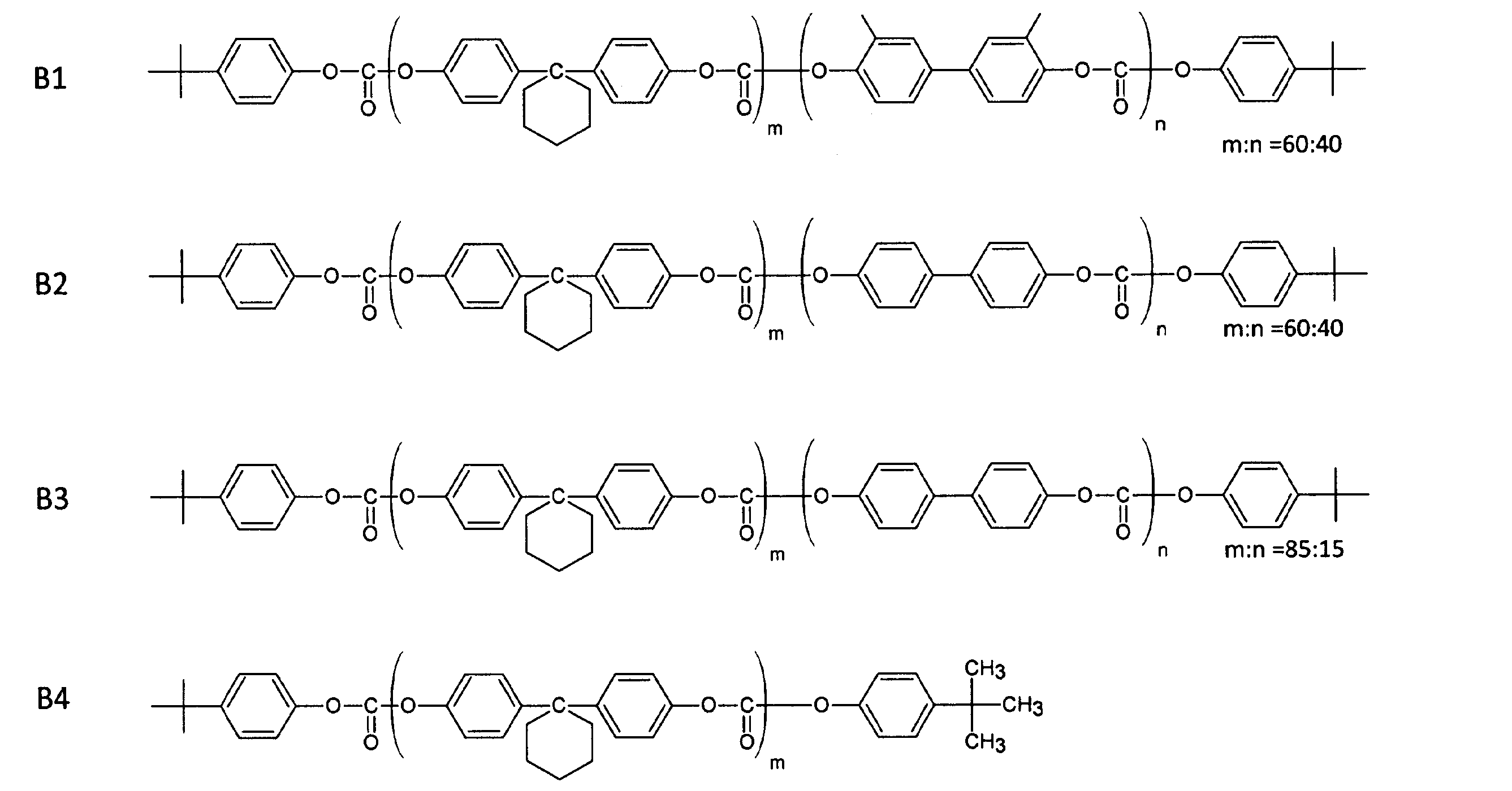
- the charge transport material, resin binder, and silane coupling agent that can be used in the embodiment of the present invention include the following charge transport materials A1 to A9, resin binders B1 to B4, and silane coupling agent C1. To C5, but is not limited thereto.
- the resin binder polycarbonate resins such as bisphenol Z type and bisphenol Z type-biphenyl copolymer as described below, and polyarylate resin can be preferably used.
- Tables 1 and 2 below show specific examples of combinations of charge transport materials A1 to A9, resin binders B1 to B4, and silane coupling agents C1 to C5 that satisfy the relationship of the solubility parameter differences ⁇ SPa and ⁇ SPb.
- the weight average molecular weight of the resin binder is preferably 5000 to 250,000, more preferably 10,000 to 200,000 in GPC (gel permeation chromatography) analysis in terms of polystyrene.
- the charge transport layer 4 contains an inorganic oxide filler surface-treated with a silane coupling agent.
- Inorganic oxide fillers include alumina, zirconia, titanium oxide, tin oxide, zinc oxide and the like, in addition to those containing silica as a main component, and these usually have a hydroxyl group on the surface during use. Therefore, when inorganic oxide fillers are mixed in the coating solution as they are, they tend to aggregate with each other, but by treating the surface of the inorganic oxide with a silane coupling agent, silane coupling to the hydroxyl group on the surface of the inorganic oxide is possible.
- the agent can be combined to reduce the cohesiveness of the inorganic oxide itself and to increase the compatibility with the resin binder and the charge transport material in the coating solution.
- a hydroxyl group may remain on the surface depending on the degree of surface treatment, which causes aggregation.
- an inorganic oxide mainly composed of silica is preferable.
- a method of producing silica particles having a particle diameter of several nanometers to several tens of nanometers as silica a method of producing water glass as a raw material called a wet method or a reaction of chlorosilane or the like called a dry method in a gas phase
- a method using an alkoxide as a silica precursor as a raw material are known.
- the purity of the silica is high because the cohesiveness of the silica is improved, and as a result, an increase in aggregates in the coating solution and the photosensitive layer is caused. Therefore, the content of metals other than the metal elements constituting the inorganic oxide is preferably controlled to 1000 ppm or less for each metal element.
- the surface treatment agent reacts with the hydroxyl group present on the surface of the silica, but if the silica contains a trace amount of other metal elements, it is adjacent to the other metal elements present on the silica surface due to the influence of the electronegativity difference between the metals. Reactivity of silanol group (hydroxyl group) is improved. Since this hydroxyl group is highly reactive with the surface treatment agent, it reacts more strongly with the surface treatment agent than other hydroxyl groups, and if remaining, causes aggregation.
- the surface treatment agent After the reaction of these surface treatment agents, the surface treatment agent reacts with other hydroxyl groups, so that the cohesiveness between silicas is reduced due to the effect of the surface treatment agent and the effect of reducing the surface charge bias due to the different metal on the surface. It is thought that it will be greatly improved.
- the inorganic oxide contains a trace amount of other metals because the reactivity of the surface treatment agent becomes better and as a result, the dispersibility by the surface treatment is improved. It can be said that the improvement in agglomeration in the case where a large amount of the foreign metal is present as an impurity and the improvement in dispersibility due to the inclusion of a very small amount of another metal are due to different mechanisms.
- silica it is suitable for surface treatment if an aluminum element is added in the range of 1000 ppm or less. Adjustment of the amount of aluminum element in silica can be carried out using the methods described in JP-A-2004-143028, JP-A-2013-224225, etc., as long as it can be controlled within a desired range.
- the adjustment method is not particularly limited.
- examples of a method for more suitably controlling the amount of aluminum element on the silica surface include the following methods. First, when producing silica fine particles, there is a method for controlling the amount of aluminum on the silica surface by, for example, adding aluminum alkoxide as an aluminum source after growing the silica particles in a shape smaller than the target silica particle diameter.
- silica fine particles are placed in a solution containing aluminum chloride, the surface of the silica fine particles is coated with an aluminum chloride solution, and this is dried and fired, or a mixed gas of an aluminum halide compound and a silicon halide compound is used. There is a method of reacting.
- the structure of silica is known to have a network-like bonded structure in which a plurality of silicon atoms and oxygen atoms are connected in a ring, and when an aluminum element is included, the number of atoms constituting the silica ring structure is Due to the effect of mixing aluminum, it becomes larger than ordinary silica. Due to this effect, the steric hindrance when the surface treatment agent reacts with the hydroxyl group on the silica surface containing aluminum element is relaxed compared to the normal silica surface, and the reactivity of the surface treatment agent is improved.
- the surface-treated silica has improved dispersibility as compared with the case where the same surface treating agent is reacted with the silica.
- silica by a wet method is more suitable for controlling the amount of aluminum element.
- the content of the aluminum element with respect to silica is preferably 1 ppm or more in consideration of the reactivity of the surface treatment agent.
- the form of the inorganic oxide is not particularly limited, but in order to reduce the cohesiveness and obtain a uniform dispersion state, the sphericity of the inorganic oxide is preferably 0.8 or more, 0.9 More preferably.
- the memory element retains the type of data to be stored depending on whether charge is accumulated or not, but the size of the accumulated charge is reduced by miniaturization and is irradiated from the outside.
- the type of data changes due to the amount of charge that changes depending on the ⁇ -ray, and as a result, unexpected data changes occur.
- the current (noise) generated by the ⁇ rays is relatively larger than the magnitude of the signal, and there is a risk of malfunction.
- a production method for reducing the amount of uranium and thorium in the inorganic oxide is described in, for example, Japanese Patent Application Laid-Open No. 2013-224225, but is not limited to this method as long as the concentration of these elements can be reduced.
- the primary particle size of the inorganic oxide filler is not particularly limited, but is preferably 1 to 200 nm, more preferably 5 to 100 nm, and still more preferably 10 to 50 nm. . If the primary particle diameter of the inorganic oxide filler is less than 1 nm, the dispersion state may become non-uniform due to aggregation. On the other hand, when the primary particle diameter of the inorganic oxide filler exceeds 200 nm, light scattering increases and image loss may occur.
- the primary particle diameter is a number average diameter measured using a scanning microscope that can directly observe the surface shape of the particles.
- the content of the surface-treated inorganic oxide filler in the charge transport layer 4 is 1 to 40% by mass, and more preferably 2 to 30% by mass with respect to the solid content of the charge transport layer 4.
- the content of the resin binder in the charge transport layer 4 is preferably 20 to 90% by mass, more preferably 30 to 80% by mass, based on the solid content of the charge transport layer 4 excluding the inorganic oxide filler.
- the content of the charge transport material in the charge transport layer 4 is preferably 10 to 80% by weight, more preferably 20 to 70% by weight, based on the solid content of the charge transport layer 4 excluding the inorganic oxide filler. is there.
- the thickness of the charge transport layer 4 is preferably in the range of 3 to 50 ⁇ m, more preferably in the range of 15 to 40 ⁇ m, in order to maintain a practically effective surface potential.
- deterioration of an antioxidant, a light stabilizer, or the like is carried out for the purpose of improving the environmental resistance and the stability against harmful light as desired.
- An inhibitor can be included.
- Compounds used for this purpose include chromanol derivatives such as tocopherol and esterified compounds, polyarylalkane compounds, hydroquinone derivatives, etherified compounds, dietherified compounds, benzophenone derivatives, benzotriazole derivatives, thioether compounds, phenylenediamine derivatives. Phosphonic acid ester, phosphorous acid ester, phenol compound, hindered phenol compound, linear amine compound, cyclic amine compound, hindered amine compound and the like.
- the charge generation layer 3 and the charge transport layer 4 may contain a leveling agent such as silicone oil or fluorine-based oil for the purpose of improving the leveling property of the formed film and imparting lubricity.
- a leveling agent such as silicone oil or fluorine-based oil for the purpose of improving the leveling property of the formed film and imparting lubricity.
- metal oxides such as silicon oxide (silica), titanium oxide, zinc oxide, calcium oxide, aluminum oxide (alumina), zirconium oxide, etc.
- metal sulfates such as barium sulfate and calcium sulfate
- metal nitride fine particles such as silicon nitride and aluminum nitride
- fluorine resin particles such as tetrafluoroethylene resin, fluorine comb-type graft polymerization resin, etc.
- other known additives can be contained as long as the electrophotographic characteristics are not significantly impaired.
- the electrophotographic photosensitive member according to the embodiment of the present invention can obtain the desired effect when applied to various machine processes.
- a charging process such as a contact charging method using a charging member such as a roller or a brush, a non-contact charging method using a corotron or a scorotron, etc., and a nonmagnetic one component, a magnetic one component, a two component, etc.
- a development system developer
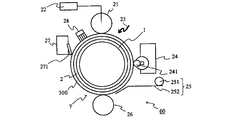
- FIG. 2 shows a schematic configuration diagram of a configuration example of the electrophotographic apparatus according to the present invention.
- the electrophotographic apparatus 60 of the embodiment of the present invention shown in the drawing includes the conductive substrate 1, the undercoat layer 2 and the photosensitive layer 300 coated on the outer peripheral surface of the photoreceptor 7 of the embodiment of the present invention. Mount.
- the electrophotographic apparatus 60 includes a roller-shaped charging member 21 disposed in the outer peripheral edge of the photoreceptor 7, a high-voltage power supply 22 that supplies an applied voltage to the charging member 21, and an image exposure member 23.
- the electrophotographic apparatus 60 may further include a cleaning device 27 including a cleaning blade 271 and a charge removal member 28.
- the electrophotographic apparatus 60 according to the embodiment of the present invention can be a color printer.
- a coating solution 1 is prepared by dissolving and dispersing 5 parts by mass of alcohol-soluble nylon (trade name “CM8000”, manufactured by Toray Industries, Inc.) and 5 parts by mass of aminosilane-treated titanium oxide fine particles in 90 parts by mass of methanol. did.
- the coating solution 1 was dip-coated on the outer periphery of an aluminum cylinder having an outer diameter of 30 mm as the conductive substrate 1 and dried at a temperature of 100 ° C. for 30 minutes to form an undercoat layer 2 having a thickness of 3 ⁇ m.
- a coating solution 2 was prepared by dissolving and dispersing in 60 parts by mass.
- the coating solution 2 was dip-coated on the undercoat layer 2 and dried at a temperature of 80 ° C. for 30 minutes to form a charge generation layer 3 having a thickness of 0.3 ⁇ m.
- the coating solution 3 was dip-coated on the charge generation layer 3 and dried at a temperature of 120 ° C. for 60 minutes to form a charge transport layer 4 having a thickness of 20 ⁇ m. Thus, a negatively charged laminated type photoreceptor was produced.
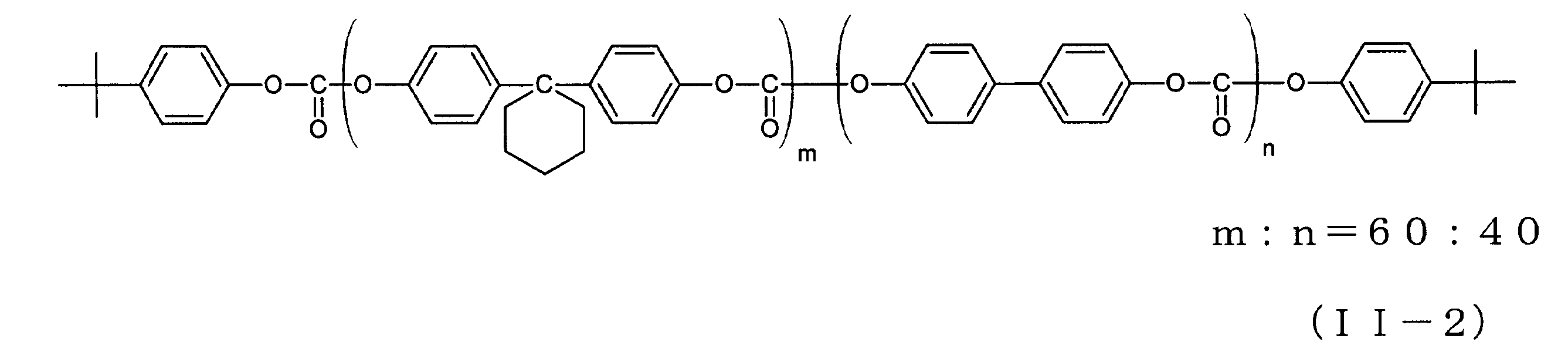
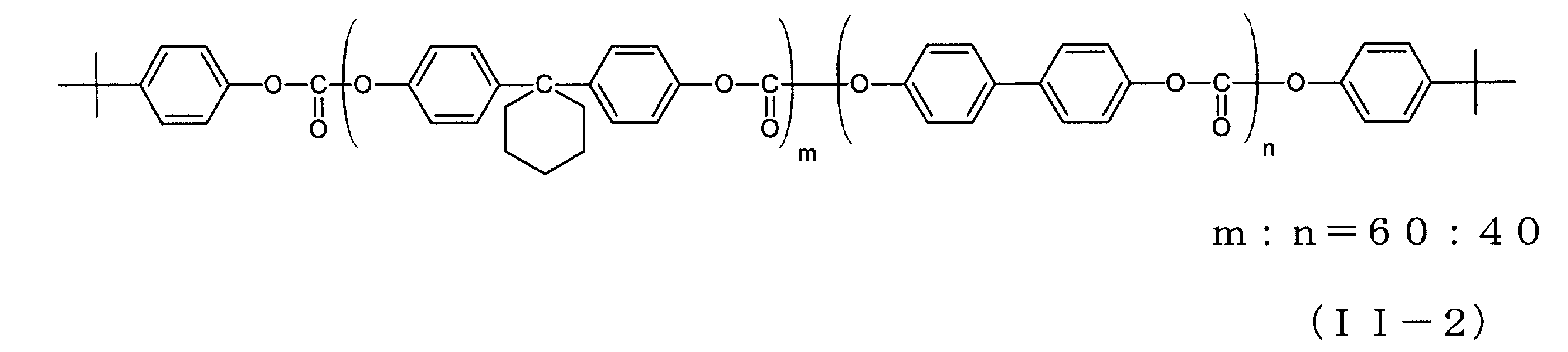
- Example 2 The resin binder (B1) represented by the structural formula (II-1) used in Example 1 is converted into the following structural formula (II-2), A photoconductor was prepared in the same manner as in Example 1 except that the resin binder (B2) shown in FIG.
- Example 3 The resin binder (B1) represented by the structural formula (II-1) used in Example 1 was replaced by the following structural formula (II-3), A photoconductor was prepared in the same manner as in Example 1 except that the resin binder (B3) shown in FIG.
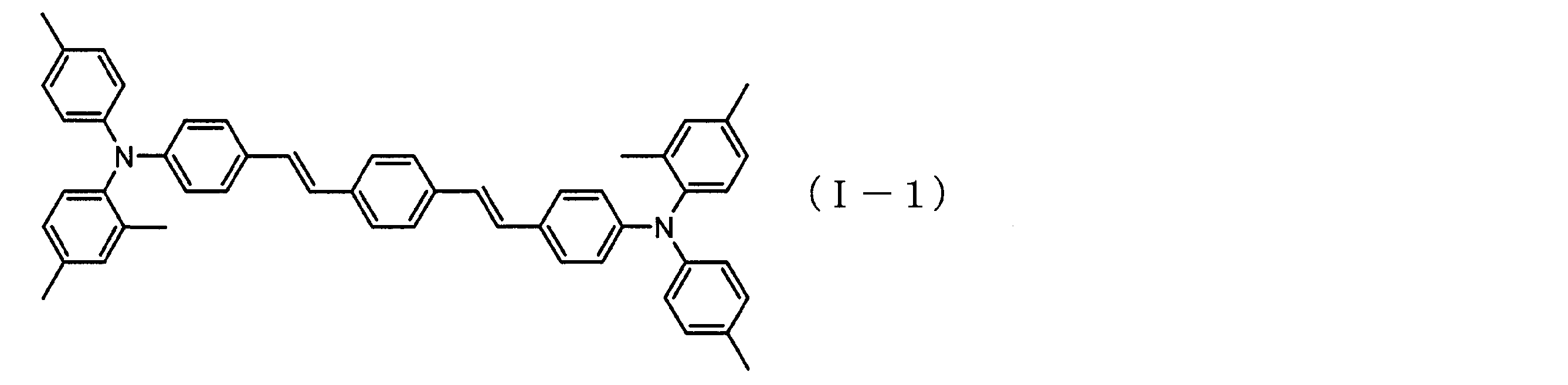
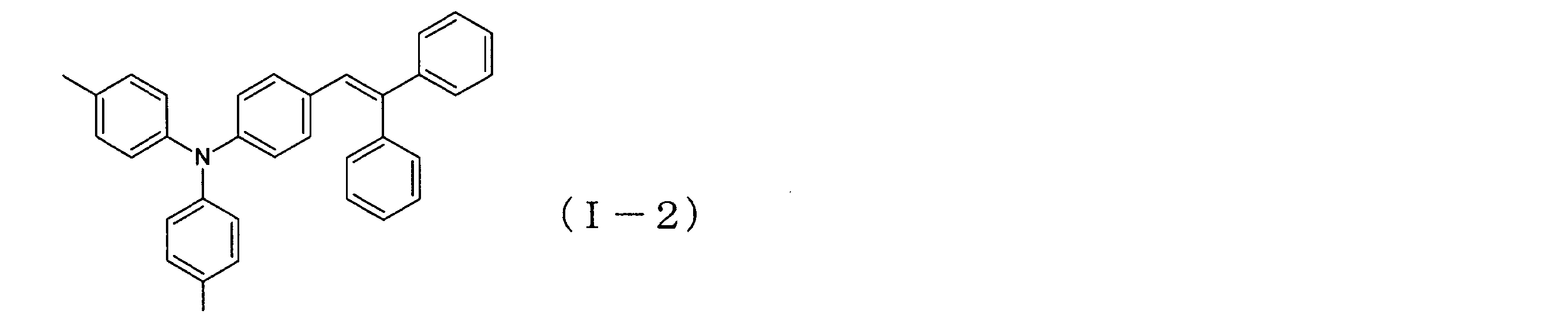
- Example 4 The charge transport material (A1) represented by the structural formula (I-1) used in Example 1 is converted into the following structural formula (I-2), A photoconductor was prepared in the same manner as in Example 1 except that the charge transport material (A2) shown in FIG.
- Example 5 The charge transport material (A1) represented by the structural formula (I-1) used in Example 1 is converted into the following structural formula (I-3), A photoconductor was prepared in the same manner as in Example 1 except that the charge transport material (A3) shown in FIG.
- Example 6 The charge transport material (A1) represented by the structural formula (I-1) used in Example 1 is converted into the following structural formula (I-4), A photoconductor was prepared in the same manner as in Example 1 except that the charge transport material (A7) shown in FIG.
- Example 7 The charge transport material (A1) represented by the structural formula (I-1) used in Example 1 is converted into the following structural formula (I-5), A photoconductor was prepared in the same manner as in Example 1 except that the charge transport material (A8) shown in FIG.
- Example 8 The charge transport material (A1) represented by the structural formula (I-1) used in Example 1 is converted into the following structural formula (I-6), A photoconductor was prepared in the same manner as in Example 1 except that the charge transport material (A9) shown in FIG.
- Example 9 The silane coupling agent (C2) represented by the structural formula (III-1) used in Example 1 was converted into the following structural formula (III-2), A photoconductor was prepared in the same manner as in Example 1 except that the silane coupling agent (C3) shown in FIG.
- Example 10 The charge transport material (A1) represented by the structural formula (I-1) used in Example 1 is converted into the following structural formula (I-2), And the resin binder (B1) represented by the structural formula (II-1) is replaced by the following structural formula (II-2), In addition, the silane coupling agent (C2) represented by the structural formula (III-1) is replaced by the following structural formula (III-3), A photoconductor was prepared in the same manner as in Example 1 except that the silane coupling agent (C4) shown in FIG.
- Example 11 The resin binder (B1) represented by the structural formula (II-1) used in Example 1 is converted into the following structural formula (II-2), And the silane coupling agent (C2) represented by the structural formula (III-1) is replaced by the following structural formula (III-4), A photoconductor was prepared in the same manner as in Example 1 except that the silane coupling agent (C5) shown in FIG.
- Example 12 The resin binder (B1) represented by the structural formula (II-1) used in Example 1 is converted into the following structural formula (II-4), And the silane coupling agent (C2) represented by the structural formula (III-1) is replaced by the following structural formula (III-4), A photoconductor was prepared in the same manner as in Example 1 except that the silane coupling agent (C5) shown in FIG.
- Example 2 The silane coupling agent (C2) represented by the structural formula (III-1) used in Example 1 was converted into the following structural formula (III-6), A photoconductor was prepared in the same manner as in Example 1 except that the silane coupling agent shown in FIG.
- Example 6 A photoconductor was prepared in the same manner as in Example 1 except that the surface-treated silica subjected to the surface treatment with the silane coupling agent used in Example 1 was not added.
- the difference ⁇ SPa in the dipole force term of the Hansen solubility parameter between the charge transport material and the silane coupling agent, and the resin binder was determined. The results are shown in Table 3 below together with the composition of each photoconductor.
- exposure light of 1.0 ⁇ W / cm 2 spectrally split at 780 nm using a filter is irradiated to the photoconductor for 5 seconds from the time when the surface potential becomes ⁇ 600 V, and the surface potential is reduced.
- the exposure amount required for light attenuation until ⁇ 300 V was evaluated as E1 / 2 ( ⁇ J / cm 2 ), and the residual potential on the surface of the photoreceptor 5 seconds after the exposure was evaluated as Vr5 (V).
- the photoconductors produced in Examples 1 to 12 and Comparative Examples 1 to 6 are mounted on an HP printer LJ4050 that has been modified so that the surface potential of the photoconductor can be measured, and 10000 sheets of A4 paper are printed.
- the film thicknesses of the front and rear photoreceptors were measured, and the average amount of wear ( ⁇ m) after printing was evaluated.
- the average amount of wear is a value obtained by measuring the film thickness at four points obtained by rotating the position of the center (130 mm from the end portion) in the longitudinal direction of the photosensitive member by 90 ° in the circumferential direction and averaging the values.
- fog and black paper density on white paper after initial printing and after printing 10,000 sheets were observed. The case where there was no fogging and no decrease in concentration was considered good.
- the charge transport layer containing the charge transport material, the resin binder, and the surface-treated inorganic oxide filler satisfying the conditions of the Hansen solubility parameter according to the present invention provides image defects while suppressing wear. It was confirmed that an electrophotographic photoreceptor capable of providing a good image without any problem can be provided.
Landscapes
- Physics & Mathematics (AREA)
- General Physics & Mathematics (AREA)
- Chemical & Material Sciences (AREA)
- Chemical Kinetics & Catalysis (AREA)
- Spectroscopy & Molecular Physics (AREA)
- Inorganic Chemistry (AREA)
- Photoreceptors In Electrophotography (AREA)
Abstract
Description
前記導電性基体上に設けられた電荷輸送層と、を備える電子写真用感光体において、
前記電荷輸送層が電荷輸送材料、樹脂バインダー、および、シランカップリング剤で表面処理された無機酸化物フィラーを含有し、
前記電荷輸送材料と前記シランカップリング剤との間の、ハンセン溶解度パラメータの双極子間力項の差ΔSPaが、ΔSPa<1.0の関係を満足し、かつ、
前記樹脂バインダーと前記シランカップリング剤との間の、ハンセン溶解度パラメータのロンドン分散力項の差ΔSPbが、ΔSPb<2.5の関係を満足する。
δp = √ΣFp2/V (J1/2/cm3/2)
(式中、Fpは各成分の双極子に関係するKreveren and Hoftyzer parameterの凝集エネルギーであり、Vは各成分のモル体積である)
また、ハンセン溶解度パラメータのロンドン分散力項δdは、次式で計算される。
δd =ΣFd/V (J1/2/cm3/2)
(式中、Fdは各成分のロンドン分散力に関係するKreveren and Hoftyzer parameterの凝集エネルギーであり、Vは各成分のモル体積である)
なお、本発明においては、上記溶解度パラメータの各項について2種の材料間の差を取るため、ハンセン溶解度パラメータの双極子間力項をSPa、ロンドン分散力項をSPbと表記する。



本発明の実施形態の電子写真装置は、上記本発明の実施形態の電子写真用感光体を搭載してなる点に特徴を有する。図2に、本発明に係る電子写真装置の一構成例の概略構成図を示す。図示する本発明の実施形態の電子写真装置60は、導電性基体1と、その外周面上に被覆された下引き層2および感光層300とを含む、本発明の実施形態の感光体7を搭載する。この電子写真装置60は、感光体7の外周縁部に配置された、図示する例ではローラ状の帯電部材21と、この帯電部材21に印加電圧を供給する高圧電源22と、像露光部材23と、現像ローラ241を備えた現像器24と、給紙ローラ251および給紙ガイド252を備えた給紙部材25と、転写帯電器(直接帯電型)26と、から構成される。電子写真装置60は、さらに、クリーニングブレード271を備えたクリーニング装置27と、除電部材28とを含んでもよい。また、本発明の実施形態の電子写真装置60は、カラープリンタとすることができる。
(実施例1)
アルコール可溶性ナイロン(東レ(株)製、商品名「CM8000」)5質量部と、アミノシラン処理された酸化チタン微粒子5質量部とを、メタノール90質量部に溶解、分散させて、塗布液1を調製した。導電性基体1としての外径30mmのアルミニウム製円筒の外周に、この塗布液1を浸漬塗工し、温度100℃で30分間乾燥して、膜厚3μmの下引き層2を形成した。


実施例1で使用した構造式(II-1)で示される樹脂バインダー(B1)を下記構造式(II-2)、
実施例1で使用した構造式(II-1)で示される樹脂バインダー(B1)を下記構造式(II-3)、

実施例1で使用した構造式(I-1)で示される電荷輸送材料(A1)を下記構造式(I-2)、
実施例1で使用した構造式(I-1)で示される電荷輸送材料(A1)を下記構造式(I-3)、

実施例1で使用した構造式(I-1)で示される電荷輸送材料(A1)を下記構造式(I-4)、

実施例1で使用した構造式(I-1)で示される電荷輸送材料(A1)を下記構造式(I-5)、

実施例1で使用した構造式(I-1)で示される電荷輸送材料(A1)を下記構造式(I-6)、

実施例1で使用した構造式(III-1)で示されるシランカップリング剤(C2)を下記構造式(III-2)、

実施例1で使用した構造式(I-1)で示される電荷輸送材料(A1)を下記構造式(I-2)、



実施例1で使用した構造式(II-1)で示される樹脂バインダー(B1)を下記構造式(II-2)、

実施例1で使用した構造式(II-1)で示される樹脂バインダー(B1)を下記構造式(II-4)、


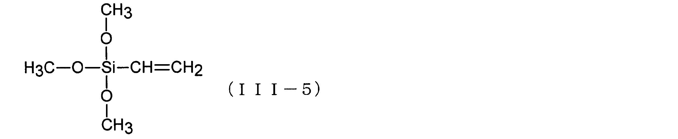
実施例1で使用した構造式(III-1)で示されるシランカップリング剤(C2)を下記構造式(III-5)、
実施例1で使用した構造式(III-1)で示されるシランカップリング剤(C2)を下記構造式(III-6)、

実施例1で使用した構造式(III-1)で示されるシランカップリング剤(C2)を下記構造式(III-7)、

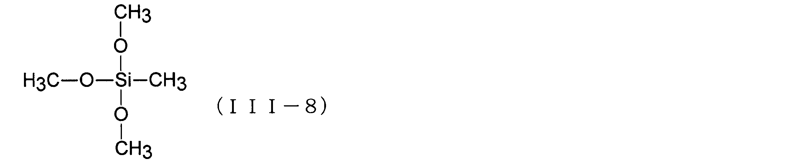
実施例1で使用した構造式(III-1)で示されるシランカップリング剤(C2)を下記構造式(III-8)、
実施例3で使用した構造式(III-1)で示されるシランカップリング剤(C2)を下記構造式(III-2)、

実施例1で使用した、シランカップリング剤による表面処理を施した表面処理シリカを添加しない以外は、実施例1と同様の方法で感光体を作製した。
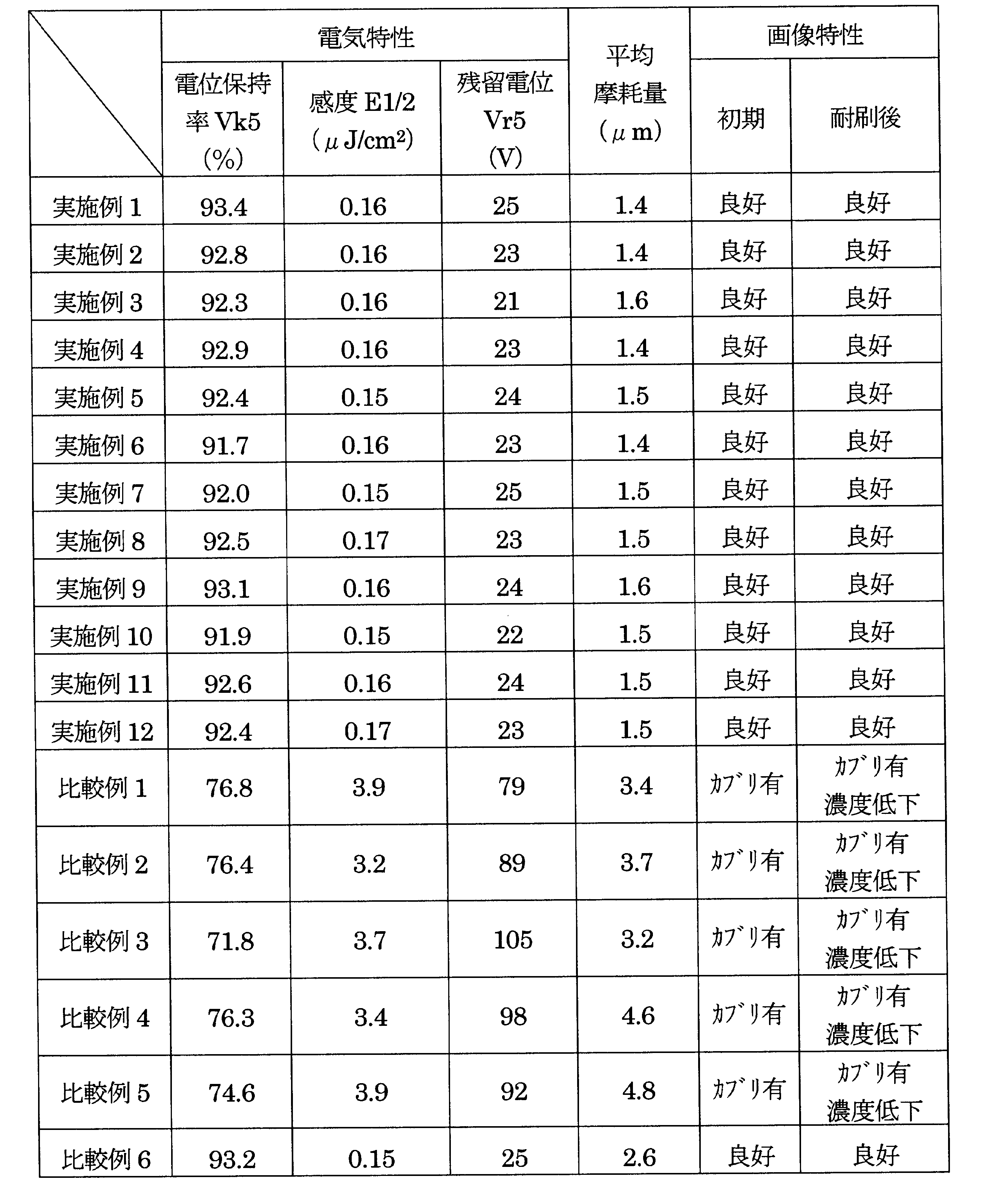
上述した実施例1~12および比較例1~6で作製した感光体の電気特性を、下記の方法で評価した。評価結果を下記の表4中に示す。
各実施例および比較例にて得られた感光体の電気特性を、ジェンテック社製のプロセスシミュレーター(CYNTHIA91)を使用して、以下の方法で評価した。実施例1~12および比較例1~6の感光体について、温度22℃、湿度50%の環境下で、感光体の表面を暗所にてコロナ放電により-650Vに帯電せしめた後、帯電直後の表面電位V0を測定した。続いて、暗所で5秒間放置後、表面電位V5を測定し、下記計算式(1)、
Vk5=V5/V0×100 (1)
に従って、帯電後5秒後における電位保持率Vk5(%)を求めた。次に、ハロゲンランプを光源とし、フィルターを用いて780nmに分光した1.0μW/cm2の露光光を、表面電位が-600Vになった時点から感光体に5秒間照射して、表面電位が-300Vとなるまで光減衰するのに要する露光量をE1/2(μJ/cm2)、露光後5秒後の感光体表面の残留電位をVr5(V)として評価した。
実施例1~12および比較例1~6において作製した感光体を、感光体の表面電位も測定できるように改造を施したHP製プリンターLJ4050に搭載して、A4用紙10000枚を印字し、印字前後の感光体の膜厚を測定し、印字後の平均摩耗量(μm)について評価を実施した。平均摩耗量は、感光体の長手方向の真ん中(端部から130mm)の位置を周方向に90°ずつ回転した4点について膜厚を測定し、平均した値である。また、初期および10000枚印字後における白紙上のカブリおよび黒紙濃度を観察した。カブリおよび濃度低下のない場合を良好とした。

2 下引き層
3 電荷発生層
4 電荷輸送層
7 感光体
21 帯電部材
22 高圧電源
23 像露光部材
24 現像器
241 現像ローラ
25 給紙部材
251 給紙ローラ
252 給紙ガイド
26 転写帯電器(直接帯電型)
27 クリーニング装置
271 クリーニングブレード
28 除電部材
60 電子写真装置
300 感光層
Claims (6)
- 導電性基体と、
前記導電性基体上に設けられた電荷輸送層と、を備える電子写真用感光体において、
前記電荷輸送層が電荷輸送材料、樹脂バインダー、および、シランカップリング剤で表面処理された無機酸化物フィラーを含有し、
前記電荷輸送材料と前記シランカップリング剤との間の、ハンセン溶解度パラメータの双極子間力項の差ΔSPaが、ΔSPa<1.0の関係を満足し、かつ、
前記樹脂バインダーと前記シランカップリング剤との間の、ハンセン溶解度パラメータのロンドン分散力項の差ΔSPbが、ΔSPb<2.5の関係を満足することを特徴とする電子写真用感光体。 - 前記樹脂バインダーが、ポリカーボネート樹脂またはポリアリレート樹脂である請求項1記載の電子写真用感光体。
- 前記無機酸化物フィラーが、1~200nmの一次粒子径を有する請求項1記載の電子写真用感光体。
- 前記電荷輸送材料が、正孔輸送材料である請求項1記載の電子写真用感光体。
- 前記導電性基体上に、少なくとも下引き層、電荷発生層および前記電荷輸送層をこの順に備える請求項1記載の電子写真用感光体。
- 請求項1記載の電子写真用感光体を搭載してなることを特徴とする電子写真装置。
Priority Applications (4)
| Application Number | Priority Date | Filing Date | Title |
|---|---|---|---|
| JP2018524902A JP6540898B2 (ja) | 2016-06-30 | 2017-04-10 | 電子写真用感光体およびそれを搭載した電子写真装置 |
| CN201780004167.7A CN108475028B (zh) | 2016-06-30 | 2017-04-10 | 电子照相用感光体及搭载有该电子照相用感光体的电子照相装置 |
| KR1020187014547A KR102058500B1 (ko) | 2016-06-30 | 2017-04-10 | 전자 사진용 감광체 및 그것을 탑재한 전자 사진 장치 |
| US15/994,597 US20180275537A1 (en) | 2016-06-30 | 2018-05-31 | Photoreceptor for electrophotography and electrophotography device having the same |
Applications Claiming Priority (2)
| Application Number | Priority Date | Filing Date | Title |
|---|---|---|---|
| JP2016-130870 | 2016-06-30 | ||
| JP2016130870 | 2016-06-30 |
Related Child Applications (1)
| Application Number | Title | Priority Date | Filing Date |
|---|---|---|---|
| US15/994,597 Continuation US20180275537A1 (en) | 2016-06-30 | 2018-05-31 | Photoreceptor for electrophotography and electrophotography device having the same |
Publications (1)
| Publication Number | Publication Date |
|---|---|
| WO2018003229A1 true WO2018003229A1 (ja) | 2018-01-04 |
Family
ID=60786267
Family Applications (1)
| Application Number | Title | Priority Date | Filing Date |
|---|---|---|---|
| PCT/JP2017/014684 Ceased WO2018003229A1 (ja) | 2016-06-30 | 2017-04-10 | 電子写真用感光体およびそれを搭載した電子写真装置 |
Country Status (6)
| Country | Link |
|---|---|
| US (1) | US20180275537A1 (ja) |
| JP (1) | JP6540898B2 (ja) |
| KR (1) | KR102058500B1 (ja) |
| CN (1) | CN108475028B (ja) |
| TW (1) | TW201802624A (ja) |
| WO (1) | WO2018003229A1 (ja) |
Cited By (3)
| Publication number | Priority date | Publication date | Assignee | Title |
|---|---|---|---|---|
| JP2020197445A (ja) * | 2019-06-03 | 2020-12-10 | 大日本印刷株式会社 | 固体物質の凝集エネルギー密度の測定方法 |
| JP2021021756A (ja) * | 2019-07-24 | 2021-02-18 | 富士電機株式会社 | 電子写真用感光体、その製造方法およびそれを搭載した電子写真装置 |
| US11586119B2 (en) | 2020-03-02 | 2023-02-21 | Fuji Electric Co., Ltd. | Electrophotographic photoconductor, method of manufacturing the same, and electrophotographic device |
Families Citing this family (1)
| Publication number | Priority date | Publication date | Assignee | Title |
|---|---|---|---|---|
| JP7004011B2 (ja) * | 2018-01-19 | 2022-01-21 | 富士電機株式会社 | 電子写真用感光体、その製造方法および電子写真装置 |
Citations (7)
| Publication number | Priority date | Publication date | Assignee | Title |
|---|---|---|---|---|
| JPH08166679A (ja) * | 1994-12-13 | 1996-06-25 | Fuji Xerox Co Ltd | 電子写真感光体およびのその製造方法 |
| JPH08202062A (ja) * | 1995-01-25 | 1996-08-09 | Konica Corp | 電子写真感光体、電子写真装置及び装置ユニット |
| JP2001117252A (ja) * | 1999-10-20 | 2001-04-27 | Fuji Xerox Co Ltd | 有機半導体膜および電子写真感光体、並びにそれを用いた画像形成装置 |
| JP2007153765A (ja) * | 2005-12-01 | 2007-06-21 | Ricoh Co Ltd | テトラヒドロキシ化合物 |
| JP2010250174A (ja) * | 2009-04-17 | 2010-11-04 | Sharp Corp | 電子写真感光体およびそれを用いた画像形成装置 |
| JP2013109298A (ja) * | 2011-11-24 | 2013-06-06 | Sharp Corp | 電子写真感光体およびそれを備えた画像形成装置 |
| JP2014191079A (ja) * | 2013-03-26 | 2014-10-06 | Mitsubishi Chemicals Corp | 電子写真感光体、電子写真プロセスカートリッジ及び画像形成装置 |
Family Cites Families (3)
| Publication number | Priority date | Publication date | Assignee | Title |
|---|---|---|---|---|
| US5679488A (en) * | 1994-11-15 | 1997-10-21 | Konica Corporation | Electrophotography photoreceptor |
| CN104169803B (zh) * | 2012-04-20 | 2018-09-04 | 富士电机株式会社 | 电子照相用感光体、其制造方法和电子照相装置 |
| JP6238718B2 (ja) * | 2013-01-25 | 2017-11-29 | キヤノン株式会社 | 電子写真感光体の製造方法 |
-
2017
- 2017-04-10 WO PCT/JP2017/014684 patent/WO2018003229A1/ja not_active Ceased
- 2017-04-10 CN CN201780004167.7A patent/CN108475028B/zh active Active
- 2017-04-10 JP JP2018524902A patent/JP6540898B2/ja active Active
- 2017-04-10 KR KR1020187014547A patent/KR102058500B1/ko active Active
- 2017-05-02 TW TW106114519A patent/TW201802624A/zh unknown
-
2018
- 2018-05-31 US US15/994,597 patent/US20180275537A1/en not_active Abandoned
Patent Citations (7)
| Publication number | Priority date | Publication date | Assignee | Title |
|---|---|---|---|---|
| JPH08166679A (ja) * | 1994-12-13 | 1996-06-25 | Fuji Xerox Co Ltd | 電子写真感光体およびのその製造方法 |
| JPH08202062A (ja) * | 1995-01-25 | 1996-08-09 | Konica Corp | 電子写真感光体、電子写真装置及び装置ユニット |
| JP2001117252A (ja) * | 1999-10-20 | 2001-04-27 | Fuji Xerox Co Ltd | 有機半導体膜および電子写真感光体、並びにそれを用いた画像形成装置 |
| JP2007153765A (ja) * | 2005-12-01 | 2007-06-21 | Ricoh Co Ltd | テトラヒドロキシ化合物 |
| JP2010250174A (ja) * | 2009-04-17 | 2010-11-04 | Sharp Corp | 電子写真感光体およびそれを用いた画像形成装置 |
| JP2013109298A (ja) * | 2011-11-24 | 2013-06-06 | Sharp Corp | 電子写真感光体およびそれを備えた画像形成装置 |
| JP2014191079A (ja) * | 2013-03-26 | 2014-10-06 | Mitsubishi Chemicals Corp | 電子写真感光体、電子写真プロセスカートリッジ及び画像形成装置 |
Cited By (6)
| Publication number | Priority date | Publication date | Assignee | Title |
|---|---|---|---|---|
| JP2020197445A (ja) * | 2019-06-03 | 2020-12-10 | 大日本印刷株式会社 | 固体物質の凝集エネルギー密度の測定方法 |
| JP7371355B2 (ja) | 2019-06-03 | 2023-10-31 | 大日本印刷株式会社 | 固体物質の凝集エネルギー密度の測定方法 |
| JP2021021756A (ja) * | 2019-07-24 | 2021-02-18 | 富士電機株式会社 | 電子写真用感光体、その製造方法およびそれを搭載した電子写真装置 |
| US11073771B2 (en) | 2019-07-24 | 2021-07-27 | Fuji Electric Co., Ltd. | Electrophotographic photoconductor, method of manufacturing the same, and electrophotographic device including the same |
| JP7346974B2 (ja) | 2019-07-24 | 2023-09-20 | 富士電機株式会社 | 電子写真用感光体、その製造方法およびそれを搭載した電子写真装置 |
| US11586119B2 (en) | 2020-03-02 | 2023-02-21 | Fuji Electric Co., Ltd. | Electrophotographic photoconductor, method of manufacturing the same, and electrophotographic device |
Also Published As
| Publication number | Publication date |
|---|---|
| CN108475028A (zh) | 2018-08-31 |
| CN108475028B (zh) | 2021-10-22 |
| JP6540898B2 (ja) | 2019-07-10 |
| TW201802624A (zh) | 2018-01-16 |
| KR102058500B1 (ko) | 2019-12-23 |
| KR20180074749A (ko) | 2018-07-03 |
| JPWO2018003229A1 (ja) | 2018-09-27 |
| US20180275537A1 (en) | 2018-09-27 |
Similar Documents
| Publication | Publication Date | Title |
|---|---|---|
| JPWO2017110300A1 (ja) | 電子写真用感光体、その製造方法および電子写真装置 | |
| JP2008299020A (ja) | 電子写真感光体、およびこれを備えた画像形成装置 | |
| JP2013257416A (ja) | 電子写真感光体、それを備えた画像形成装置およびプロセスカートリッジ | |
| JP6540898B2 (ja) | 電子写真用感光体およびそれを搭載した電子写真装置 | |
| JP4288949B2 (ja) | 電子写真感光体、画像形成装置、画像形成方法及びプロセスカートリッジ | |
| JP2015225231A (ja) | 電子写真感光体およびそれを備えた画像形成装置 | |
| JP6583579B1 (ja) | 電子写真用感光体の製造方法 | |
| JP5636728B2 (ja) | 電子写真感光体、電子写真感光体カートリッジ、及び画像形成装置 | |
| JP4411232B2 (ja) | 電子写真感光体の製造方法 | |
| JP2008146076A (ja) | 電子写真感光体及びこれを含む電子写真画像の形成装置 | |
| JP7346974B2 (ja) | 電子写真用感光体、その製造方法およびそれを搭載した電子写真装置 | |
| JP2003177561A (ja) | 電子写真感光体、画像形成方法、画像形成装置及びプロセスカートリッジ | |
| JP3994638B2 (ja) | 電子写真感光体、画像形成方法、画像形成装置、及びプロセスカートリッジ | |
| JP2003345045A (ja) | 電子写真感光体、画像形成装置、画像形成方法及びプロセスカートリッジ | |
| JP2003316047A (ja) | 有機感光体、画像形成装置、画像形成方法及びプロセスカートリッジ | |
| JP2017182063A (ja) | 電子写真感光体、電子写真感光体カートリッジ、及び画像形成装置 | |
| JP2022124375A (ja) | 電子写真感光体、その製造方法および電子写真装置 | |
| JP5585668B2 (ja) | 電子写真用感光体、その製造方法および電子写真装置 | |
| JP5196996B2 (ja) | 単層型電子写真感光体及び画像形成装置 | |
| JP2005140947A (ja) | 電子写真感光体およびそれを用いた電子写真装置 | |
| JP2015138159A (ja) | 電子写真感光体および画像形成装置 | |
| JP2009122321A (ja) | 電子写真感光体、画像形成方法、画像形成装置及びプロセスカートリッジ | |
| WO2012111672A1 (ja) | 電子写真用感光体、その製造方法および電子写真装置 | |
| JP2014222279A (ja) | 電子写真感光体の製造方法 | |
| JP2015114351A (ja) | 電子写真感光体およびそれを用いた画像形成装置 |
Legal Events
| Date | Code | Title | Description |
|---|---|---|---|
| ENP | Entry into the national phase |
Ref document number: 20187014547 Country of ref document: KR Kind code of ref document: A |
|
| ENP | Entry into the national phase |
Ref document number: 2018524902 Country of ref document: JP Kind code of ref document: A |
|
| 121 | Ep: the epo has been informed by wipo that ep was designated in this application |
Ref document number: 17819597 Country of ref document: EP Kind code of ref document: A1 |
|
| NENP | Non-entry into the national phase |
Ref country code: DE |
|
| 122 | Ep: pct application non-entry in european phase |
Ref document number: 17819597 Country of ref document: EP Kind code of ref document: A1 |