WO2017221896A1 - トンネル磁気抵抗素子及びその製造方法 - Google Patents
トンネル磁気抵抗素子及びその製造方法 Download PDFInfo
- Publication number
- WO2017221896A1 WO2017221896A1 PCT/JP2017/022551 JP2017022551W WO2017221896A1 WO 2017221896 A1 WO2017221896 A1 WO 2017221896A1 JP 2017022551 W JP2017022551 W JP 2017022551W WO 2017221896 A1 WO2017221896 A1 WO 2017221896A1
- Authority
- WO
- WIPO (PCT)
- Prior art keywords
- magnetic layer
- layer
- magnetic field
- magnetoresistive element
- heat treatment
- Prior art date
- Legal status (The legal status is an assumption and is not a legal conclusion. Google has not performed a legal analysis and makes no representation as to the accuracy of the status listed.)
- Ceased
Links
Images














Classifications
-
- H—ELECTRICITY
- H10—SEMICONDUCTOR DEVICES; ELECTRIC SOLID-STATE DEVICES NOT OTHERWISE PROVIDED FOR
- H10N—ELECTRIC SOLID-STATE DEVICES NOT OTHERWISE PROVIDED FOR
- H10N50/00—Galvanomagnetic devices
- H10N50/80—Constructional details
- H10N50/85—Materials of the active region
-
- H—ELECTRICITY
- H01—ELECTRIC ELEMENTS
- H01F—MAGNETS; INDUCTANCES; TRANSFORMERS; SELECTION OF MATERIALS FOR THEIR MAGNETIC PROPERTIES
- H01F10/00—Thin magnetic films, e.g. of one-domain structure
- H01F10/08—Thin magnetic films, e.g. of one-domain structure characterised by magnetic layers
- H01F10/10—Thin magnetic films, e.g. of one-domain structure characterised by magnetic layers characterised by the composition
- H01F10/12—Thin magnetic films, e.g. of one-domain structure characterised by magnetic layers characterised by the composition being metals or alloys
-
- H—ELECTRICITY
- H01—ELECTRIC ELEMENTS
- H01F—MAGNETS; INDUCTANCES; TRANSFORMERS; SELECTION OF MATERIALS FOR THEIR MAGNETIC PROPERTIES
- H01F10/00—Thin magnetic films, e.g. of one-domain structure
- H01F10/08—Thin magnetic films, e.g. of one-domain structure characterised by magnetic layers
- H01F10/10—Thin magnetic films, e.g. of one-domain structure characterised by magnetic layers characterised by the composition
- H01F10/12—Thin magnetic films, e.g. of one-domain structure characterised by magnetic layers characterised by the composition being metals or alloys
- H01F10/13—Amorphous metallic alloys, e.g. glassy metals
-
- H—ELECTRICITY
- H01—ELECTRIC ELEMENTS
- H01F—MAGNETS; INDUCTANCES; TRANSFORMERS; SELECTION OF MATERIALS FOR THEIR MAGNETIC PROPERTIES
- H01F41/00—Apparatus or processes specially adapted for manufacturing or assembling magnets, inductances or transformers; Apparatus or processes specially adapted for manufacturing materials characterised by their magnetic properties
- H01F41/14—Apparatus or processes specially adapted for manufacturing or assembling magnets, inductances or transformers; Apparatus or processes specially adapted for manufacturing materials characterised by their magnetic properties for applying magnetic films to substrates
- H01F41/18—Apparatus or processes specially adapted for manufacturing or assembling magnets, inductances or transformers; Apparatus or processes specially adapted for manufacturing materials characterised by their magnetic properties for applying magnetic films to substrates by cathode sputtering
-
- H—ELECTRICITY
- H01—ELECTRIC ELEMENTS
- H01F—MAGNETS; INDUCTANCES; TRANSFORMERS; SELECTION OF MATERIALS FOR THEIR MAGNETIC PROPERTIES
- H01F41/00—Apparatus or processes specially adapted for manufacturing or assembling magnets, inductances or transformers; Apparatus or processes specially adapted for manufacturing materials characterised by their magnetic properties
- H01F41/14—Apparatus or processes specially adapted for manufacturing or assembling magnets, inductances or transformers; Apparatus or processes specially adapted for manufacturing materials characterised by their magnetic properties for applying magnetic films to substrates
- H01F41/22—Heat treatment; Thermal decomposition; Chemical vapour deposition
-
- H—ELECTRICITY
- H10—SEMICONDUCTOR DEVICES; ELECTRIC SOLID-STATE DEVICES NOT OTHERWISE PROVIDED FOR
- H10N—ELECTRIC SOLID-STATE DEVICES NOT OTHERWISE PROVIDED FOR
- H10N50/00—Galvanomagnetic devices
- H10N50/01—Manufacture or treatment
-
- H—ELECTRICITY
- H10—SEMICONDUCTOR DEVICES; ELECTRIC SOLID-STATE DEVICES NOT OTHERWISE PROVIDED FOR
- H10N—ELECTRIC SOLID-STATE DEVICES NOT OTHERWISE PROVIDED FOR
- H10N50/00—Galvanomagnetic devices
- H10N50/10—Magnetoresistive devices
Definitions
- the present invention relates to a tunnel magnetoresistive element and a manufacturing method thereof.
- a tunnel magnetoresistive element (TMR (Tunnel Magneto Resistive) element) includes a pinned magnetic layer whose magnetization direction is fixed, a free magnetic layer whose magnetization direction changes under the influence of an external magnetic field, and a pinned magnetic layer And an insulating layer disposed between the magnetic layer and the free magnetic layer to form a magnetic tunnel junction (MTJ (Magnetic Tunnel Junction)).
- MTJ Magnetic Tunnel Junction
- the resistance of the insulating layer is changed by the tunnel effect according to the angular difference between the magnetization direction of the pinned magnetic layer and the magnetization direction of the free magnetic layer.
- Examples of using the tunnel magnetoresistive element include a magnetic memory, a magnetic head, and a magnetic sensor. (Patent Documents 1-5).
- a soft magnetic layer NiFe, CoFeSiB, etc.
- a soft magnetic layer NiFe, CoFeSiB, etc.
- a magnetic coupling layer Ti
- Ru a synthetic bond that generates only a magnetic bond is used while eliminating a solid physical bond between the magnetic tunnel junction and the soft magnetic material
- the present invention has been made in view of the above problems in the prior art, and an object of the present invention is to improve the structure of the free magnetic layer of the tunnel magnetoresistive element and realize a magnetoresistive characteristic with high linearity.
- the invention according to claim 1 for solving the above-described problems is a pinned magnetic layer in which the magnetization direction is fixed, a free magnetic layer whose magnetization direction changes under the influence of an external magnetic field, and the pinned layer
- a magnetic tunnel junction is formed by an insulating layer disposed between the magnetic layer and the free magnetic layer, and a tunnel effect is applied according to an angular difference between the magnetization direction of the pinned magnetic layer and the magnetization direction of the free magnetic layer.
- a tunnel magnetoresistive element that changes the resistance of an insulating layer From the side close to the substrate supporting the magnetic layer and the insulating layer, the pinned magnetic layer, the insulating layer, and the free magnetic layer are laminated in this order.
- the free magnetic layer is a tunnel magnetoresistive element having a ferromagnetic layer whose lower surface is joined to the insulating layer, and a soft magnetic layer laminated in contact with the upper surface of the ferromagnetic layer.
- the easy magnetization axes of the ferromagnetic layer and the soft magnetic layer constituting the free magnetic layer are in the same direction and are different from the easy magnetization axis of the pinned magnetic layer.
- the invention according to claim 3 is the tunnel magnetoresistive element according to claim 1 or 2, wherein the soft magnetic layer constituting the free magnetic layer is made of a ferromagnetic alloy. .
- the invention according to claim 4 is characterized in that the soft magnetic layer constituting the free magnetic layer is made of an alloy of permalloy (NiFe, NiFeCuMO, NiFeC ⁇ MO) or amorphous (CoFeSiB, CoFeCrSiB, CoFeNiSiB, NiFeSiB).
- the invention according to claim 5 is the tunnel magnetoresistive element according to claim 1 or 2, wherein the soft magnetic layer constituting the free magnetic layer is made of a ferrimagnetic alloy. .
- the invention according to claim 6 is the tunnel magnetoresistive element according to claim 1 or 2, wherein the soft magnetic layer constituting the free magnetic layer is made of a ferrite alloy.
- the invention according to claim 7 is characterized in that the soft magnetic layer constituting the free magnetic layer is made of an alloy of microcrystals (NiCuNbSiB, NiCuZrB, NiAlSiNiSrB). This is a tunnel magnetoresistive element.
- the invention according to claim 8 is the tunnel magnetoresistive element according to any one of claims 1 to 7, wherein the insulating layer is made of a material having a coherent tunnel effect. .
- the invention according to claim 9 is characterized in that the insulating layer is formed of any one of magnesium oxide, spinel, and aluminum oxide. This is a tunnel magnetoresistive element.
- the invention according to claim 10 is a method of manufacturing the tunnel magnetoresistive element according to any one of claims 1 to 9,
- the laminated magnetic layer and the insulating layer are laminated on the substrate, and the ferromagnetic layer constituting the free magnetic layer is laminated, and heat treatment is performed while applying an external magnetic field to the free layer.
- a tunnel magnetoresistive element manufacturing method comprising: a film forming step in a magnetic field in which an easy axis of magnetization of the free magnetic layer is formed in a different direction with respect to the easy axis of magnetization of the pinned magnetic layer.
- the invention according to claim 11 is a second heat treatment step in a magnetic field in which, after the film formation step in the magnetic field, heat treatment is performed while applying an external magnetic field in the same direction as in the film formation step in the magnetic field, 11.
- the horizontal axis represents the external magnetic field (H (Oe)), and the vertical axis represents the rate of change in resistance of the tunnel magnetoresistive element (TMR ratio (%)).
- H (Oe) the external magnetic field
- TMR ratio (%) the rate of change in resistance of the tunnel magnetoresistive element
- FIG. 6B is a cross-sectional view of the multilayer structure showing the manufacturing process of the tunnel magnetoresistive element according to the embodiment of the present invention following FIG. 6B. It is a graph which shows the magnetoresistive characteristic of the tunnel magnetoresistive element which concerns on one Embodiment of this invention. The horizontal axis represents the external magnetic field (H (Oe)), and the vertical axis represents the rate of change in resistance of the tunnel magnetoresistive element (TMR ratio (%)). It is a graph which shows the magnetoresistive characteristic of the tunnel magnetoresistive element which concerns on one Embodiment of this invention, and shows the thing after implementing the 2nd, 3rd heat processing process in a magnetic field.
- H external magnetic field
- TMR ratio rate of change in resistance of the tunnel magnetoresistive element
- the case where the heat treatment temperature of the second heat treatment step in the magnetic field is 200 ° C. and the heat treatment temperature of the third heat treatment step in the magnetic field is 180 ° C. is shown.
- the horizontal axis represents the external magnetic field (H (Oe)), and the vertical axis represents the rate of change in resistance of the tunnel magnetoresistive element (TMR ratio (%)).
- H (Oe) the external magnetic field
- TMR ratio (%) the rate of change in resistance of the tunnel magnetoresistive element
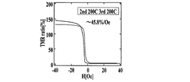
- the case where the heat treatment temperature in the second magnetic field heat treatment step is 200 ° C. and the heat treatment temperature in the third magnetic field heat treatment step is 200 ° C. is shown.
- FIG. 9B is a surface view of the multilayer structure showing the manufacturing process of the tunneling magneto-resistance element according to one example of the present invention following FIG. 9A.
- FIG. 9B is a cross-sectional view of the multilayer structure showing the manufacturing process of the tunnel magnetoresistive element according to one example of the present invention, following FIG. 9A.
- FIG. 9B is a cross-sectional view of the multilayer structure showing the manufacturing process of the tunnel magnetoresistive element according to one example of the present invention, following FIG. 9A.
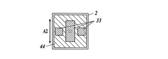
- FIG. 9B is a surface view of the multilayer structure showing the manufacturing process of the tunneling magneto-resistance element according to one example of the present invention following FIG. 9B.
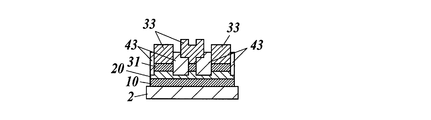
- FIG. 9B is a cross-sectional view of the stacked structure showing the manufacturing process of the tunnel magnetoresistive element according to one example of the present invention following FIG. 9B.
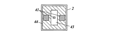
- FIG. 9D is a surface view of the multilayer structure showing the manufacturing process of the tunnel magnetoresistive element according to the example of the present invention following FIG. 9C.
- FIG. 9C is a cross-sectional view of the multilayer structure showing the manufacturing process of the tunnel magnetoresistive element according to the example of the present invention following FIG. 9C.
- FIG. 9C is a cross-sectional view of the multilayer structure showing the manufacturing process of the tunnel magnetoresistive element according to the example of the present invention following FIG. 9C.
- FIG. 9D is a surface view of the multilayer structure showing the manufacturing process of the tunneling magneto-resistance element according to one example of the present invention following FIG. 9D.
- FIG. 9D is a cross-sectional view of the multilayer structure illustrating the manufacturing process of the tunnel magnetoresistive element according to the example of the present invention following FIG. 9D.
- FIG. 9E is a surface view of the multilayer structure showing the manufacturing process of the tunnel magnetoresistive element according to the example of the present invention following FIG. 9E.
- FIG. 9E is a cross-sectional view of the multilayer structure showing the manufacturing process of the tunnel magnetoresistive element according to the example of the present invention following FIG. 9E.
- FIG. 9F is a surface view of the laminated structure, following FIG.
- FIG. 9F showing the manufacturing process of the tunnel magnetoresistive element according to one example of the present invention.
- FIG. 9F is a cross-sectional view of the multilayer structure illustrating the manufacturing process of the tunnel magnetoresistive element according to the example of the present invention following FIG. 9F.
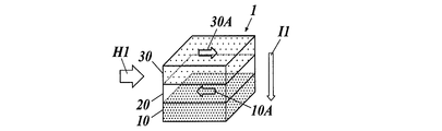
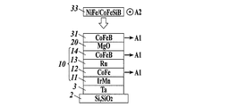
- the tunnel magnetoresistive element 1 includes a fixed magnetic layer 10 whose magnetization direction is fixed, a free magnetic layer 30 whose magnetization direction changes under the influence of an external magnetic field, and a fixed magnetic layer A magnetic tunnel junction is formed by the insulating layer 20 disposed between the magnetic layer 10 and the free magnetic layer 30, and tunneling is performed according to an angular difference between the magnetization direction of the pinned magnetic layer 10 and the magnetization direction of the free magnetic layer 30.
- the resistance of the insulating layer 20 is changed by the effect.
- FIG. 1A to 1C show the magnetization direction 10A of the pinned magnetic layer 10 and the magnetization direction 30A of the free magnetic layer 30 in each magnetic field state shown in FIG. 1D.
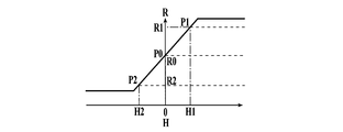
- 1A shows a state in which the detected magnetic field is zero (neutral position, position P0 on the graph of FIG. 1D)
- FIG. 1B shows a state in which a predetermined plus magnetic field is loaded (position P1 on the graph of FIG. 1D)
- FIG. 1C shows a state in which a predetermined negative magnetic field is loaded (position P2 on the graph of FIG. 1D).
- the magnetization direction 10A of the pinned magnetic layer 10 and the magnetization direction 30A of the free magnetic layer 30 are stable at a twist position of approximately 90 degrees. This is because each magnetized in the direction of the easy axis. That is, the tunnel magnetoresistive element 1 shown in FIGS. 1A to 1C is formed at a position where the easy magnetization axis of the free magnetic layer 30 is twisted by approximately 90 degrees with respect to the easy magnetization axis of the pinned magnetic layer 10.
- An arrow 10A shown in 1A indicates the direction of the easy axis of magnetization of the pinned magnetic layer 10
- an arrow 30A indicates the direction of the easy axis of magnetization of the free magnetic layer 30.
- the magnetization direction 10A of the pinned magnetic layer 10 is constant without being affected by the change of the external magnetic field, and the magnetization direction 30A of the free magnetic layer 30 is the external magnetic field (H1, H2). Changes under the influence.
- FIG. 1B when an external magnetic field H1 in the opposite direction to the magnetization direction 10A of the pinned magnetic layer 10 is applied to the tunnel magnetoresistive element 1, the magnetization direction 30A of the free magnetic layer 30 changes to the pinned magnetic layer. 10 spins in the direction opposite to the magnetization direction 10A, and the resistance of the insulating layer 20 increases due to the tunnel effect (the resistance increases from R0 to R1 in FIG. 1D).
- the change in resistance is schematically shown by the thickness of the arrows of the currents I0, I1, and I2 in FIGS. 1A-1C.
- FIG. 1C when an external magnetic field H2 having the same direction as the magnetization direction 10A of the pinned magnetic layer 10 is applied to the tunnel magnetoresistive element 1, the magnetization direction 30A of the free magnetic layer 30 changes to the pinned magnetic layer. 10 spins in the same direction as the magnetization direction 10A, and the resistance of the insulating layer 20 decreases due to the tunnel effect (the resistance decreases from R0 to R2 in FIG. 1D).
- FIG. 1C when an external magnetic field H2 having the same direction as the magnetization direction 10A of the pinned magnetic layer 10 is applied to the tunnel magnetoresistive element 1, the magnetization direction 30A of the free magnetic layer 30 changes to the pinned magnetic layer. 10 spins in the same direction as the magnetization direction 10A, and the resistance of the insulating layer 20 decreases due to the tunnel effect (the resistance decreases from R0 to R2 in
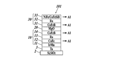
- a conventional tunnel magnetoresistive element 101 shown in FIG. 2 is of the kind described in Patent Documents 1-5, in which a pinned magnetic layer 10 is formed below the insulating layer 20 and a free magnetic layer 30 is formed on the top.
- the layer 30 has a laminated structure in which a magnetic coupling layer (Ru) 32 is interposed between a ferromagnetic layer (CoFeB) 31 and a soft magnetic layer (NiFe or CoFeSi) 33.
- a base layer (Ta) 3 is formed on a substrate (Si, SiO 2 ) 2 and an antiferromagnetic layer (from the bottom) is formed as a pinned magnetic layer 10 thereon.
- the laminated structure includes a ferromagnetic layer (CoFeB) 31, a magnetic coupling layer (Ru) 32, and a soft magnetic layer (NiFe or CoFeSi) 33 laminated from below.
- a conventional tunnel magnetoresistive element 101 the direction of the easy axis of magnetization of all the magnetic layers can be obtained even if the heat treatment in the magnetic field is performed a plurality of times while applying the external magnetic field while changing the direction each time.
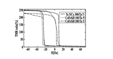
- the magnetoresistive characteristics have a high hysteresis as shown in FIG. 3, and the above-described linearity cannot be realized.
- the arrow A1 shown in FIG. 2 is the direction of the easy axis of magnetization of the magnetic layer.
- the conventional tunnel magnetoresistive element 102 shown in FIG. 4 is of the kind described in Patent Document 6, and has a laminated structure in which the fixed magnetic layer 10 and the free magnetic layer 30 are turned upside down with respect to FIG. .
- the direction of the easy magnetization axis (arrow A1) of the free magnetic layer 30 is formed in a direction different from the direction of the easy magnetization axis of the pinned magnetic layer 10 (arrow A2).
- the shape of the free magnetic layer 30 can be increased (Hk is improved and noise is expected to be reduced), but the upper insulating layer 20 and the fixed magnetic layer 10 are adversely affected (because of deterioration of uniformity and crystallinity). It was difficult to improve the performance as a magnetic sensor.
- the tunnel magnetoresistive element 1A of the present invention is fixed from the side close to the substrate 2 that supports the magnetic layers 10 and 30 and the insulating layer 20, similarly to the conventional tunnel magnetoresistive element 101.
- the magnetic layer 10, the insulating layer 20, and the free magnetic layer 30 are stacked in this order, and the magnetic coupling layer (Ru) 32 is removed from the conventional stacked structure of the tunnel magnetoresistive element 101.
- a laminated structure having a ferromagnetic layer 31 bonded to the insulating layer 20 and a soft magnetic layer 33 laminated in contact with the upper surface of the ferromagnetic layer 31 is employed.
- the easy magnetization axes of the ferromagnetic layer 31 and the soft magnetic layer 33 constituting the free magnetic layer 30 are in the same direction, and are different from the easy magnetization axis of the pinned magnetic layer 10 ( It can be formed to have a magnetization characteristic at a twisted position (for example, a direction twisted approximately 90 degrees), and the linearity described above can be realized.
- the laminated body is subjected to a heat treatment while applying an external magnetic field in a predetermined direction (arrow A1), and free magnetic
- a first heat treatment process in a magnetic field is performed in which the easy axis of the ferromagnetic layer 31 constituting the layer 30 and the easy axis of the pinned magnetic layer 10 are formed in the same direction.
- the easy magnetization axis of the free magnetic layer 30 is different from the easy magnetization axis of the pinned magnetic layer 10 (for example, a direction twisted approximately 90 degrees).
- a film formation step in the magnetic field to be formed is performed to obtain a stacked structure shown in FIG. 6C.
- the easy axis of magnetization of the ferromagnetic layer 31 and the soft magnetic layer 33 constituting the free magnetic layer 30 are the same through the first heat treatment process in the magnetic field and the film formation process in the magnetic field.
- the easy magnetization axis of the pinned magnetic layer 10 is formed in the magnetic field direction (arrow A1) applied during the first heat treatment process in the magnetic field, and the easy magnetization axis of the free magnetic layer 30 is formed in the film formation process in the magnetic field. It is formed in the magnetic field direction (arrow A2) applied at the time. At this point, a linear magnetoresistive characteristic as shown in FIG. 7 is obtained.
- a second heat treatment process in a magnetic field is performed in which heat treatment is performed while applying an external magnetic field in the same direction (arrow A2) as in the film formation process in a magnetic field.
- a third heat treatment process in the magnetic field is performed in which the heat treatment is performed while applying the external magnetic field in the same direction as the first heat treatment process in the magnetic field (arrow A1).
- FIGS. 9A-9G2 An embodiment of a manufacturing process according to the main points of the manufacturing process will now be described with reference to FIGS. 9A-9G2.
- 9A-9G2 the illustration of the underlayer 3 is omitted.
- a first magnetic field heat treatment step is performed on the ferromagnetic tunnel junction (MTJ) multilayer film (layers 10, 20, 31) formed on the substrate 2 (FIG. 9A).
- the direction of the magnetic field to be applied is the direction of arrow A1
- the strength of the magnetic field is 1T
- the heat treatment temperature is 375 ° C.
- This heat treatment greatly improves the tunnel magnetoresistance (TMR) ratio, which is the rate of change in resistance.
- TMR tunnel magnetoresistance
- a resist pattern is formed on the surface of the MTJ multilayer film subjected to the first heat treatment process in a magnetic field by photolithography or electron beam lithography (photolithography in this embodiment) (FIGS. 9B1 and 9B2).
- the layer 41 is a Ta layer formed on the ferromagnetic layer 31 and is formed before the first magnetic field heat treatment step.
- a resist pattern 42 is formed on the Ta layer 41.
- Ar ion milling is performed on the MTJ multilayer film on which the resist pattern 42 is formed, and etching is performed up to the MgO insulating layer 20 (FIGS. 9B1 and 9B2). Since the MTJ multilayer film directly under the resist pattern 42 is not exposed to Ar ions, the multilayer film structure remains up to the uppermost layer, and the formed resist-shaped MTJ pillars are formed (FIGS. 9B1 and 9B2).
- An interlayer insulating layer 43 is formed to electrically insulate the MTJ pillar from the soft magnetic layer 33 and the upper electrode layer formed in a later process, and to allow current to flow only in the MTJ pillar portion (FIGS. 9C1 and 9C2).
- a material of the interlayer insulating layer 43 SiO 2 or Al—Ox can be used (in this embodiment, SiO 2 is used).
- a lift-off method or a contact hole forming method can be used (in this embodiment, a lift-off method). In the lift-off method, an insulating film such as SiO 2 is formed on the entire substrate while leaving the resist pattern 42 for MTJ pillar formation.
- a sputtering method or low-temperature CVD can be used for forming the insulating film (low-temperature CVD is used in this embodiment).
- the resist 42 is removed by ultrasonically cleaning the substrate with an organic solvent such as acetone or dimethylpyrrolidone.
- an organic solvent such as acetone or dimethylpyrrolidone.
- the MTJ pillar forming resist pattern 42 is removed with an organic solvent or the like, and an insulating film is formed on the entire substrate.
- a resist pattern having openings where only electrical contacts on the MTJ pillar are required is formed, and reactive etching is performed using CHF3, CH4, or the like as a process gas, thereby forming openings in the insulating film.
- reactive etching is performed using CHF3, CH4, or the like as a process gas, thereby forming openings in the insulating film.
- a resist pattern 44 is formed on the substrate on which the interlayer insulating layer 43 is formed by photolithography using the soft magnetic layer 33 and the mask for forming the upper electrode (FIGS. 9D1 and 9D2). Pattern formation is performed using the region where the soft magnetic layer 33 and the upper electrode layer are formed as an opening. Etching by Ar ion milling is performed on the substrate on which the soft magnetic layer 33 and the upper electrode layer forming resist pattern 44 are formed to expose the upper CoFeB ferromagnetic layer 31 in the MTJ multilayer film (FIGS. 9E1 and 9E2). . By forming the soft magnetic layer 33 on the exposed CoFeB layer 31, soft magnetic characteristics are exhibited in the magnetoresistance curve.
- the soft magnetic layer 33 can be made of an amorphous material such as CoFeSiB or a soft magnetic material such as a NiFe alloy (CoFeSiB is used in this embodiment).
- the magnetic multilayer film below the MTJ and the upper part are formed.
- the easy axis of magnetization of the CoFeB layer 31 and the soft magnetic layer 33 can be twisted to 90 degrees, whereby the resistance linearly changes with respect to the magnetic field component in the hard axis direction of the free magnetic layer 30.
- a magnetoresistive curve with linearity as shown is obtained.
- the substrate 2 is made of Si, SiO 2 , Ta is 5 nm, Ru is 10 nm, IrMn is 10 nm, CoFe is 2 nm, Ru is 0.85 nm, CoFeB is 3 nm, MgO is 2.7 nm, CoFeB.
- a soft magnetic layer (CoFeSiB) 33 was formed by sputtering in a magnetic field to a film thickness of 100 nm.
- the upper electrode layer is formed (FIGS. 9G1 and 9G2).
- As the upper electrode layer material Ta, Al, Cu, Au and the like and multilayer films thereof can be used (Ta / Al multilayer film in this embodiment).
- the upper electrode layer prevents oxidation of the soft magnetic layer 33 and is responsible for electrical connection with a power supply circuit, an amplifier circuit, and the like during sensor operation.
- the substrate on which the soft magnetic layer 33 and the upper electrode are formed is ultrasonically cleaned using an organic solvent or the like, and the resist 44 is removed, thereby removing the soft magnetic layer 33 and the upper electrode layer other than the resist opening (FIG. 9G1, 9G2). Therefore, the soft magnetic layer 33 and the upper electrode layer can be formed into arbitrary shapes by photolithography.
- the tunnel magnetoresistive element is manufactured by the above microfabrication, the soft magnetic layer 33 is in an as-deposited state in which heat treatment is not performed after the element is manufactured. Therefore, it is possible to develop a magnetoresistive curve having softer magnetic characteristics by performing heat treatment in the magnetic field again on the manufactured element and manipulating the magnetic anisotropy of the soft magnetic layer 33.
- a heat treatment in a rotating magnetic field or a heat treatment in which the magnetic field direction is changed from the hard axis of the soft magnetic layer 33 to the easy axis the Hk of the soft magnetic layer 33 is reduced, and higher magnetic field sensitivity is obtained.
- the second magnetic field heat treatment step is performed with the magnetic field direction set to a direction of 90 degrees (arrow A2 direction) with respect to the direction during the first magnetic field heat treatment step (arrow A1 direction).
- a third heat treatment process in a magnetic field was performed in the 0 degree direction (arrow A1 direction).
- the heat treatment temperature was 200 ° C.
- the heat treatment temperature in the third heat treatment step in a magnetic field was 200 ° C.
- the magnetoresistance curve shown in FIG. 8B was obtained.
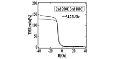
- FIG. 8A shows a case where the heat treatment temperature in the second magnetic field heat treatment step is 200 ° C. and the heat treatment temperature in the third magnetic field heat treatment step is 180 ° C.
- the tunnel magnetoresistive element of the present invention is different from the conventional element structure in that the soft magnetic layer is sputtered after the MTJ multilayer film is subjected to the first heat treatment process in the magnetic field.
- the soft magnetic layer does not adversely affect the process of developing a high TMR ratio by intermediate heat treatment. Therefore, a wide range of material choices for the soft magnetic layer can be provided, and the most suitable material for the application and ease of use, such as ferrimagnetic (eg, permalloy or amorphous), ferromagnetic (eg, ferrite), and microcrystalline alloys. Should be selected.
- the free magnetic layer of the conventional tunnel magnetoresistive element has a limit of a film thickness of several nm to several hundred nm, but the soft magnetic layer of several ⁇ m is bonded to the free magnetic layer of the tunnel magnetoresistive element of the present invention.
- the volume of the soft magnetic layer can be very large. Therefore, it can be expected to produce a magnetic sensor having a high SN ratio by greatly reducing white noise and 1 / f noise due to thermal fluctuation of the free magnetic layer.
- the free magnetic layer is located on the outermost surface of the element, the shape can be freely provided. Therefore, it is expected to produce a tunnel magnetoresistive element with a built-in flux concentrator (FC) that concentrates the magnetic flux on the free magnetic layer.
- FC built-in flux concentrator
- the tunnel magnetoresistive element and the FC are manufactured with a physically separated structure.
- the free magnetic layer and the FC are joined as a thin film or an integrated structure, so that the magnetic flux concentration effect is obtained. It is available to the maximum.
- the present invention can be used for a tunnel magnetoresistive element and a manufacturing method thereof.
Landscapes
- Engineering & Computer Science (AREA)
- Power Engineering (AREA)
- Manufacturing & Machinery (AREA)
- Physics & Mathematics (AREA)
- Thermal Sciences (AREA)
- Hall/Mr Elements (AREA)
- Thin Magnetic Films (AREA)
Abstract
トンネル磁気抵抗素子の自由磁性層の構造を改善し、リニアリティの高い磁気抵抗特性を実現する。基板2に近い側から、固定磁性層10、絶縁層20、自由磁性層30の順で積層され、自由磁性層は、下面を絶縁層に接合する強磁性層31、及び当該強磁性層の上面に接触して積層された軟磁性層33を有する。自由磁性層を構成する強磁性層及び軟磁性層の磁化容易軸(A2)は互いに同方向にあり、かつ、固定磁性層の磁化容易軸(A1)に対して異なる方向にある
Description
本発明は、トンネル磁気抵抗素子及びその製造方法に関する。
トンネル磁気抵抗素子(TMR(Tunnel Magneto Resistive)素子)は、磁化の向きが固定された固定磁性層、外部からの磁場の影響を受けて磁化の向きが変化する自由磁性層、及び、固定磁性層と自由磁性層との間に配置された絶縁層を有し、磁気トンネル接合(MTJ(Magnetic Tunnel Junction))を形成する。固定磁性層の磁化の向きと自由磁性層の磁化の向きとの角度差に従ってトンネル効果により絶縁層の抵抗を変化させる。このトンネル磁気抵抗素子を利用したものとして、磁気メモリ・磁気ヘッド・磁気センサーなどが挙げられる。(特許文献1-5)。
また、自由磁性層に、外部からの磁場に反応しやすい軟磁性層(NiFeやCoFeSiBなど)を配置し、基板に近い側から、自由磁性層、絶縁層、固定磁性層の順に積層した構造を磁場中熱処理することで、外部からの磁場によって引き起こされる固定磁性層の磁化の向きと自由磁性層の磁化の向きとの角度差に従ってトンネル効果により絶縁層の抵抗変化を利用した、リニアリティの高い高感度な磁気センサーを作製する技術がある(特許文献6)
自由磁性層には、外部からの磁場に反応しやすい軟磁性層(NiFeやCoFeSiBなど)を配置し、さらに、絶縁層に接合する強磁性層と軟磁性層との間に磁気結合層(TaやRu)を介在させることで、磁気トンネル接合と軟磁性材料との固体物性上の結合は排除しつつ、磁気的な結合のみ発生させるシンセティック結合が利用されている(特許文献1-6)。
また、自由磁性層に、外部からの磁場に反応しやすい軟磁性層(NiFeやCoFeSiBなど)を配置し、基板に近い側から、自由磁性層、絶縁層、固定磁性層の順に積層した構造を磁場中熱処理することで、外部からの磁場によって引き起こされる固定磁性層の磁化の向きと自由磁性層の磁化の向きとの角度差に従ってトンネル効果により絶縁層の抵抗変化を利用した、リニアリティの高い高感度な磁気センサーを作製する技術がある(特許文献6)
自由磁性層には、外部からの磁場に反応しやすい軟磁性層(NiFeやCoFeSiBなど)を配置し、さらに、絶縁層に接合する強磁性層と軟磁性層との間に磁気結合層(TaやRu)を介在させることで、磁気トンネル接合と軟磁性材料との固体物性上の結合は排除しつつ、磁気的な結合のみ発生させるシンセティック結合が利用されている(特許文献1-6)。
しかしながら、本発明者らの研究によると、特許文献6に記載の構成では、さらに感度を高める為、自由磁性層の形状を大きく(Hkが改善、ノイズが低減すると期待)すると、上層の絶縁層や固定磁性層に悪影響(均一性や結晶性の悪化が原因と予想される)が生じ、磁気センサーとしての性能を高めることが困難になっている。
一方で、絶縁層や固定磁性層に悪影響を与えず、自由磁性層の形状を大きくする為には、特許文献1,2,4,5の構成の様に、基板に近い側から、固定磁性層、絶縁層、自由磁性層の順に積層すれば良い。しかし、この構造の場合、熱処理処理によってリニアリティの高い高精度な磁気センサーを実現するに至っていない。磁気抵抗素子を、磁場の強弱を精度よく計測する磁気センサーとして使用していくためには検出磁場ゼロの状態(中立位置)からプラス磁場、マイナス磁場の変化に応じて上下に比例的に抵抗変化を起こす性質(リニアリティ)が求められる。
一方で、絶縁層や固定磁性層に悪影響を与えず、自由磁性層の形状を大きくする為には、特許文献1,2,4,5の構成の様に、基板に近い側から、固定磁性層、絶縁層、自由磁性層の順に積層すれば良い。しかし、この構造の場合、熱処理処理によってリニアリティの高い高精度な磁気センサーを実現するに至っていない。磁気抵抗素子を、磁場の強弱を精度よく計測する磁気センサーとして使用していくためには検出磁場ゼロの状態(中立位置)からプラス磁場、マイナス磁場の変化に応じて上下に比例的に抵抗変化を起こす性質(リニアリティ)が求められる。
本発明は以上の従来技術における問題に鑑みてなされたものであって、トンネル磁気抵抗素子の自由磁性層の構造を改善し、リニアリティの高い磁気抵抗特性を実現することを課題とする。
以上の課題を解決するための請求項1記載の発明は、磁化の向きが固定された固定磁性層、外部からの磁場の影響を受けて磁化の向きが変化する自由磁性層、及び、前記固定磁性層と前記自由磁性層との間に配置された絶縁層により、磁気トンネル接合を形成し、前記固定磁性層の磁化の向きと前記自由磁性層の磁化の向きとの角度差に従ってトンネル効果により絶縁層の抵抗を変化させるトンネル磁気抵抗素子であって、
前記磁性層及び絶縁層を支持する基板に近い側から、前記固定磁性層、前記絶縁層、前記自由磁性層の順で積層され、
前記自由磁性層は、下面を前記絶縁層に接合する強磁性層、及び当該強磁性層の上面に接触して積層された軟磁性層を有することを特徴とするトンネル磁気抵抗素子である。
前記磁性層及び絶縁層を支持する基板に近い側から、前記固定磁性層、前記絶縁層、前記自由磁性層の順で積層され、
前記自由磁性層は、下面を前記絶縁層に接合する強磁性層、及び当該強磁性層の上面に接触して積層された軟磁性層を有することを特徴とするトンネル磁気抵抗素子である。
請求項2記載の発明は、前記自由磁性層を構成する前記強磁性層及び前記軟磁性層の磁化容易軸は互いに同方向にあり、かつ、前記固定磁性層の磁化容易軸に対して異なる方向にあることを特徴とする請求項1に記載のトンネル磁気抵抗素子である。
請求項3記載の発明は、前記自由磁性層を構成する前記軟磁性層がフェロ磁性の合金で構成されていることを特徴とする請求項1又は請求項2に記載のトンネル磁気抵抗素子である。
請求項4記載の発明は、前記自由磁性層を構成する前記軟磁性層がパーマロイ(NiFe, NiFeCuMο, NiFeCοMο)又はアモルファス(CoFeSiB, CoFeCrSiB, CoFeNiSiB, NiFeSiB)の合金で構成されていることを特徴とする請求項1又は請求項2に記載のトンネル磁気抵抗素子である。
請求項5記載の発明は、前記自由磁性層を構成する前記軟磁性層がフェリ磁性の合金で構成されていることを特徴とする請求項1又は請求項2に記載のトンネル磁気抵抗素子である。
請求項6記載の発明は、前記自由磁性層を構成する前記軟磁性層がフェライト合金で構成されていることを特徴とする請求項1又は請求項2に記載のトンネル磁気抵抗素子である。
請求項7記載の発明は、前記自由磁性層を構成する前記軟磁性層が微結晶(NiCuNbSiB, NiCuZrB, NiAlSiNiSrB)の合金で構成されていることを特徴とする請求項1又は請求項2に記載のトンネル磁気抵抗素子である。
請求項8記載の発明は、前記絶縁層は、コヒーレントトンネル効果をもつ材料で形成されていることを特徴とする請求項1から請求項7のうちいずれか一に記載のトンネル磁気抵抗素子である。
請求項9記載の発明は、前記絶縁層は、酸化マグネシウム、スピネル、及び酸化アルミニウムのいずれか1つで形成されていることを特徴とする請求項1から請求項7のうちいずれか一に記載のトンネル磁気抵抗素子である。
請求項10記載の発明は、請求項1から請求項9のうちいずれか一に記載のトンネル磁気抵抗素子を製造する方法であって、
前記基板上に前記固定磁性層及び前記絶縁層を積層し、さらに前記自由磁性層を構成する前記強磁性層を積層した後の積層体に対し、外部磁場を印加しながら熱処理を行い、前記自由磁性層を構成する前記強磁性層の磁化容易軸と前記固定磁性層の磁化容易軸とを同方向に形成する第1の磁場中熱処理工程と、
前記第1の磁場中熱処理工程の後、前記第1の磁場中熱処理工程のときとは向きを異ならせて外部磁場を印加しながら前記自由磁性層を構成する前記軟磁性層を成膜することで、前記自由磁性層の磁化容易軸を、前記固定磁性層の磁化容易軸に対して異なる方向に形成する磁場中成膜工程とを備えるトンネル磁気抵抗素子の製造方法である。
前記基板上に前記固定磁性層及び前記絶縁層を積層し、さらに前記自由磁性層を構成する前記強磁性層を積層した後の積層体に対し、外部磁場を印加しながら熱処理を行い、前記自由磁性層を構成する前記強磁性層の磁化容易軸と前記固定磁性層の磁化容易軸とを同方向に形成する第1の磁場中熱処理工程と、
前記第1の磁場中熱処理工程の後、前記第1の磁場中熱処理工程のときとは向きを異ならせて外部磁場を印加しながら前記自由磁性層を構成する前記軟磁性層を成膜することで、前記自由磁性層の磁化容易軸を、前記固定磁性層の磁化容易軸に対して異なる方向に形成する磁場中成膜工程とを備えるトンネル磁気抵抗素子の製造方法である。
請求項11記載の発明は、前記磁場中成膜工程の後、前記磁場中成膜工程のときと同じ方向に外部磁場を印加しながら熱処理を行う第2の磁場中熱処理工程と、
前記第2の磁場中熱処理工程の後、前記第1の磁場中熱処理工程のときと同じ方向に外部磁場を印加しながら熱処理を行う第3の磁場中熱処理工程とを備える請求項10に記載のトンネル磁気抵抗素子の製造方法である。
前記第2の磁場中熱処理工程の後、前記第1の磁場中熱処理工程のときと同じ方向に外部磁場を印加しながら熱処理を行う第3の磁場中熱処理工程とを備える請求項10に記載のトンネル磁気抵抗素子の製造方法である。
本発明によれば、リニアリティの高い磁気抵抗特性を実現することができる。
以下に本発明の一実施形態につき図面を参照して説明する。以下は本発明の一実施形態であって本発明を限定するものではない。
まず、図1A-1Dを参照してトンネル磁気抵抗素子の基本構造及び本発明が実現しようとする理想的な磁気抵抗特性につき説明する。
図1A-1Cに示すようにトンネル磁気抵抗素子1は、磁化の向きが固定された固定磁性層10、外部からの磁場の影響を受けて磁化の向きが変化する自由磁性層30、及び、固定磁性層10と自由磁性層30との間に配置された絶縁層20により、磁気トンネル接合を形成し、固定磁性層10の磁化の向きと自由磁性層30の磁化の向きとの角度差に従ってトンネル効果により絶縁層20の抵抗を変化させるものである。
図1A-1Cは、図1Dに示す各磁場状態における固定磁性層10の磁化の向き10Aと自由磁性層30の磁化の向き30Aを示す。図1Aは検出磁場ゼロの状態(中立位置、図1Dのグラフ上の位置P0)におけるものを、図1Bは所定のプラス磁場が負荷された状態(図1Dのグラフ上の位置P1)におけるものを、図1Cは所定のマイナス磁場が負荷された状態(図1Dのグラフ上の位置P2)におけるものを示す。
図1Aは検出磁場ゼロの状態(中立位置P0)においては、固定磁性層10の磁化の向き10Aと自由磁性層30の磁化の向き30Aとが略90度のねじれの位置で安定している。これは、それぞれ磁化容易軸の方向に磁化しているからである。すなわち、図1A-Cに示すトンネル磁気抵抗素子1は、自由磁性層30の磁化容易軸が固定磁性層10の磁化容易軸に対して略90度ねじれた位置に形成されたものであり、図1Aに示す矢印10Aが固定磁性層10の磁化容易軸の方向を、矢印30Aが自由磁性層30磁化容易軸の方向を示している。
図1A-1Cに示すように固定磁性層10の磁化の向き10Aは、外部磁場の変化に影響されず一定であり、自由磁性層30の磁化の向き30Aは、外部磁場(H1,H2)の影響を受けて変化する。
図1Bに示すように、固定磁性層10の磁化の向き10Aに対して反対方向の外部磁場H1がトンネル磁気抵抗素子1に印加されると、自由磁性層30の磁化の向き30Aが固定磁性層10の磁化の向き10Aの逆方向側へスピンし、トンネル効果により絶縁層20の抵抗が増大する(図1Dで抵抗がR0からR1に増加)。抵抗の変化を図1A-1Cにおいて電流I0、I1,I2の矢印の太さで模式的に示す。
図1Cに示すように、固定磁性層10の磁化の向き10Aに対して同方向の外部磁場H2がトンネル磁気抵抗素子1に印加されると、自由磁性層30の磁化の向き30Aが固定磁性層10の磁化の向き10Aと同方向側へスピンし、トンネル効果により絶縁層20の抵抗が減少する(図1Dで抵抗がR0からR2に減少)。
図1Dに示すように抵抗(縦軸)を増大させる方向にも、減少させる方向にも、外部磁場の強さに対して比例的に(グラフが直線的に)抵抗変化を起こす性質(リニアリティ)を有するトンネル磁気抵抗素子1を実現したい。
図1A-1Cに示すようにトンネル磁気抵抗素子1は、磁化の向きが固定された固定磁性層10、外部からの磁場の影響を受けて磁化の向きが変化する自由磁性層30、及び、固定磁性層10と自由磁性層30との間に配置された絶縁層20により、磁気トンネル接合を形成し、固定磁性層10の磁化の向きと自由磁性層30の磁化の向きとの角度差に従ってトンネル効果により絶縁層20の抵抗を変化させるものである。
図1A-1Cは、図1Dに示す各磁場状態における固定磁性層10の磁化の向き10Aと自由磁性層30の磁化の向き30Aを示す。図1Aは検出磁場ゼロの状態(中立位置、図1Dのグラフ上の位置P0)におけるものを、図1Bは所定のプラス磁場が負荷された状態(図1Dのグラフ上の位置P1)におけるものを、図1Cは所定のマイナス磁場が負荷された状態(図1Dのグラフ上の位置P2)におけるものを示す。
図1Aは検出磁場ゼロの状態(中立位置P0)においては、固定磁性層10の磁化の向き10Aと自由磁性層30の磁化の向き30Aとが略90度のねじれの位置で安定している。これは、それぞれ磁化容易軸の方向に磁化しているからである。すなわち、図1A-Cに示すトンネル磁気抵抗素子1は、自由磁性層30の磁化容易軸が固定磁性層10の磁化容易軸に対して略90度ねじれた位置に形成されたものであり、図1Aに示す矢印10Aが固定磁性層10の磁化容易軸の方向を、矢印30Aが自由磁性層30磁化容易軸の方向を示している。
図1A-1Cに示すように固定磁性層10の磁化の向き10Aは、外部磁場の変化に影響されず一定であり、自由磁性層30の磁化の向き30Aは、外部磁場(H1,H2)の影響を受けて変化する。
図1Bに示すように、固定磁性層10の磁化の向き10Aに対して反対方向の外部磁場H1がトンネル磁気抵抗素子1に印加されると、自由磁性層30の磁化の向き30Aが固定磁性層10の磁化の向き10Aの逆方向側へスピンし、トンネル効果により絶縁層20の抵抗が増大する(図1Dで抵抗がR0からR1に増加)。抵抗の変化を図1A-1Cにおいて電流I0、I1,I2の矢印の太さで模式的に示す。
図1Cに示すように、固定磁性層10の磁化の向き10Aに対して同方向の外部磁場H2がトンネル磁気抵抗素子1に印加されると、自由磁性層30の磁化の向き30Aが固定磁性層10の磁化の向き10Aと同方向側へスピンし、トンネル効果により絶縁層20の抵抗が減少する(図1Dで抵抗がR0からR2に減少)。
図1Dに示すように抵抗(縦軸)を増大させる方向にも、減少させる方向にも、外部磁場の強さに対して比例的に(グラフが直線的に)抵抗変化を起こす性質(リニアリティ)を有するトンネル磁気抵抗素子1を実現したい。
図2に示す従来例のトンネル磁気抵抗素子101は、特許文献1-5に記載の類のもので、絶縁層20の下部に固定磁性層10、上部に自由磁性層30が形成され、自由磁性層30は、強磁性層(CoFeB)31と軟磁性層(NiFe又はCoFeSi)33との間に磁気結合層(Ru)32が介在する積層構造である。
詳しくは、従来例のトンネル磁気抵抗素子101は、基板(Si,SiO2)2上に、下地層(Ta)3が形成され、その上に固定磁性層10として、下から反強磁性層(IrMn)11、強磁性層(CoFe)12、磁気結合層(Ru)13、強磁性層(CoFeB)14が積層され、絶縁層(MgO)20を介して、その上に、自由磁性層30として、下から強磁性層(CoFeB)31、磁気結合層(Ru)32、軟磁性層(NiFe又はCoFeSi)33が積層された積層構造を有する。
このような従来例のトンネル磁気抵抗素子101にあっては、都度向きを異ならせて外部磁場を印加しながら熱処理する磁場中熱処理を複数回行っても、すべての磁性層の磁化容易軸の方向が揃って磁気抵抗特性が図3に示すようなヒステリシスの高い形態となってしまい、上述したリニアリティを実現できない。図2に示す矢印A1が磁性層の磁化容易軸の方向である。
詳しくは、従来例のトンネル磁気抵抗素子101は、基板(Si,SiO2)2上に、下地層(Ta)3が形成され、その上に固定磁性層10として、下から反強磁性層(IrMn)11、強磁性層(CoFe)12、磁気結合層(Ru)13、強磁性層(CoFeB)14が積層され、絶縁層(MgO)20を介して、その上に、自由磁性層30として、下から強磁性層(CoFeB)31、磁気結合層(Ru)32、軟磁性層(NiFe又はCoFeSi)33が積層された積層構造を有する。
このような従来例のトンネル磁気抵抗素子101にあっては、都度向きを異ならせて外部磁場を印加しながら熱処理する磁場中熱処理を複数回行っても、すべての磁性層の磁化容易軸の方向が揃って磁気抵抗特性が図3に示すようなヒステリシスの高い形態となってしまい、上述したリニアリティを実現できない。図2に示す矢印A1が磁性層の磁化容易軸の方向である。
一方、図4に示す従来例のトンネル磁気抵抗素子102は、特許文献6に記載の類のもので、図2に対し固定磁性層10と自由磁性層30とを上下逆にした積層構造を有する。 このような従来例のトンネル磁気抵抗素子102にあっては、自由磁性層30の磁化容易軸の方向(矢印A1)を固定磁性層10の容易磁化軸の方向(矢印A2)と異なる方向に形成できるとともに、自由磁性層30の形状を大きく(Hkが改善、ノイズが低減すると期待)することができるが、上層の絶縁層20や固定磁性層10に悪影響(均一性や結晶性の悪化が原因と予想される)が生じ、磁気センサーとしての性能を高めることが困難になった。
そこで、図5に示すように本発明のトンネル磁気抵抗素子1Aは、従来例のトンネル磁気抵抗素子101と同様に、磁性層10,30及び絶縁層20を支持する基板2に近い側から、固定磁性層10、絶縁層20、自由磁性層30の順で積層され、従来例のトンネル磁気抵抗素子101の積層構造に対し磁気結合層(Ru)32を排し、自由磁性層30は、下面を絶縁層20に接合する強磁性層31、及び当該強磁性層31の上面に接触して積層された軟磁性層33を有する積層構造とする。
かかる積層構造によれば、自由磁性層30を構成する強磁性層31及び軟磁性層33の磁化容易軸は互いに同方向にあり、かつ、固定磁性層10の磁化容易軸に対して異なる方向(ねじれの位置、例えば略90度ねじれた方向)にある磁化特性に形成することができ、上述したリニアリティを実現できる。
かかる積層構造によれば、自由磁性層30を構成する強磁性層31及び軟磁性層33の磁化容易軸は互いに同方向にあり、かつ、固定磁性層10の磁化容易軸に対して異なる方向(ねじれの位置、例えば略90度ねじれた方向)にある磁化特性に形成することができ、上述したリニアリティを実現できる。
(製造プロセス要点)
そのための、製造方法の要点を説明する。
まず、図6Aに示すように、基板2から少なくとも強磁性層31までの層を積層した後、この積層体に対し、所定方向(矢印A1)の外部磁場を印加しながら熱処理を行い、自由磁性層30を構成する強磁性層31の磁化容易軸と固定磁性層10の磁化容易軸とを同方向に形成する第1の磁場中熱処理工程を実施する。
かかる第1の磁場中熱処理工程の後、図6Bに示すように第1の磁場中熱処理工程のときとは向きをねじるように異ならせて(矢印A2方向にした)外部磁場を印加しながら自由磁性層30を構成する軟磁性層33を成膜することで、自由磁性層30の磁化容易軸を、固定磁性層10の磁化容易軸に対して異なる方向(例えば略90度ねじれた方向)に形成する磁場中成膜工程を実施し、図6Cに示す積層構造を得る。
図6Cに示すように、以上の第1の磁場中熱処理工程、磁場中成膜工程を経ることで、自由磁性層30を構成する強磁性層31及び軟磁性層33の磁化容易軸は互いに同方向にあり、かつ、固定磁性層10の磁化容易軸に対して異なる方向(好ましくは略90度ねじれた方向)にある磁化特性に形成することができる。すなわち、固定磁性層10の磁化容易軸は、第1の磁場中熱処理工程のときに印加された磁場方向(矢印A1)に形成され、自由磁性層30の磁化容易軸は、磁場中成膜工程のときに印加された磁場方向(矢印A2)に形成される。
この時点で、図7に示すようなリニアリティのある磁気抵抗特性が得られる。
そのための、製造方法の要点を説明する。
まず、図6Aに示すように、基板2から少なくとも強磁性層31までの層を積層した後、この積層体に対し、所定方向(矢印A1)の外部磁場を印加しながら熱処理を行い、自由磁性層30を構成する強磁性層31の磁化容易軸と固定磁性層10の磁化容易軸とを同方向に形成する第1の磁場中熱処理工程を実施する。
かかる第1の磁場中熱処理工程の後、図6Bに示すように第1の磁場中熱処理工程のときとは向きをねじるように異ならせて(矢印A2方向にした)外部磁場を印加しながら自由磁性層30を構成する軟磁性層33を成膜することで、自由磁性層30の磁化容易軸を、固定磁性層10の磁化容易軸に対して異なる方向(例えば略90度ねじれた方向)に形成する磁場中成膜工程を実施し、図6Cに示す積層構造を得る。
図6Cに示すように、以上の第1の磁場中熱処理工程、磁場中成膜工程を経ることで、自由磁性層30を構成する強磁性層31及び軟磁性層33の磁化容易軸は互いに同方向にあり、かつ、固定磁性層10の磁化容易軸に対して異なる方向(好ましくは略90度ねじれた方向)にある磁化特性に形成することができる。すなわち、固定磁性層10の磁化容易軸は、第1の磁場中熱処理工程のときに印加された磁場方向(矢印A1)に形成され、自由磁性層30の磁化容易軸は、磁場中成膜工程のときに印加された磁場方向(矢印A2)に形成される。
この時点で、図7に示すようなリニアリティのある磁気抵抗特性が得られる。
さらに上記磁場中成膜工程の後、次の工程を実施することが好ましい。すなわち、磁場中成膜工程のときと同じ方向(矢印A2)に外部磁場を印加しながら熱処理を行う第2の磁場中熱処理工程を実施する。さらに、第2の磁場中熱処理工程の後、第1の磁場中熱処理工程のときと同じ方向(矢印A1)に外部磁場を印加しながら熱処理を行う第3の磁場中熱処理工程を実施する。これにより、図8に示すようにHk,Hcを小さくして高感度化を図ることができる。
(製造プロセスの実施例)
ここで、上記製造プロセスの要点に従った製造プロセスの一実施例を、図9A-9G2を参照しつつ説明する。図9A-9G2において下地層3の図示を省略する。
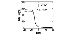
基板2上に成膜された強磁性トンネル接合(Magnetic Tunnel Junction : MTJ)多層膜(層10,20,31)に対して第1の磁場中熱処理工程を行う(図9A)。印加する磁場方向を矢印A1方向とし、磁場の強さを1Tとし、熱処理温度を375℃とする。この熱処理によって抵抗変化率であるトンネル磁気抵抗(Tunnel Magneto-Resistance : TMR)比が大きく向上する。
ここで、上記製造プロセスの要点に従った製造プロセスの一実施例を、図9A-9G2を参照しつつ説明する。図9A-9G2において下地層3の図示を省略する。
基板2上に成膜された強磁性トンネル接合(Magnetic Tunnel Junction : MTJ)多層膜(層10,20,31)に対して第1の磁場中熱処理工程を行う(図9A)。印加する磁場方向を矢印A1方向とし、磁場の強さを1Tとし、熱処理温度を375℃とする。この熱処理によって抵抗変化率であるトンネル磁気抵抗(Tunnel Magneto-Resistance : TMR)比が大きく向上する。
第1の磁場中熱処理工程を行ったMTJ多層膜表面にフォトリソグラフィもしくは電子線リソグラフィ(本実施例ではフォトリソグラフィ)によってレジストパターン形成を行う(図9B1,9B2)。層41は強磁性層31上に形成されたTa層で、第1の磁場中熱処理工程前に形成したものである。Ta層41上にレジストパターン42を形成する。
レジストパターン42を形成したMTJ多層膜に対して、Arイオンミリングを行い、MgO絶縁層20までエッチングを行う(図9B1,9B2)。レジストパターン42直下のMTJ多層膜はArイオンに晒されないため最上部層まで多層膜構造が残り、形成されたレジスト形状のMTJピラーが形成される(図9B1,9B2)。
レジストパターン42を形成したMTJ多層膜に対して、Arイオンミリングを行い、MgO絶縁層20までエッチングを行う(図9B1,9B2)。レジストパターン42直下のMTJ多層膜はArイオンに晒されないため最上部層まで多層膜構造が残り、形成されたレジスト形状のMTJピラーが形成される(図9B1,9B2)。
MTJピラーと後のプロセスで成膜する軟磁性層33及び上部電極層を電気的に絶縁し、MTJピラー部分にのみ電流を流すため、層間絶縁層43の形成する(図9C1,9C2)。層間絶縁層43の材料は、SiO2やAl-Oxを用いることができる(本実施例はSiO2を使用)。層間絶縁層43の形成プロセスとして、リフトオフ法やコンタクトホール形成法を用いることができる(本実施例ではリフトオフ法)。リフトオフ法では、MTJピラー形成用のレジストパターン42を残したまま、基板全体にSiO2等の絶縁膜を成膜する。絶縁膜の成膜にはスパッタリング法や低温CVDを用いることができる(本実施例では低温CVDを使用)。絶縁膜の成膜後、基板をアセトンやジメチルピロリドン等の有機溶媒で超音波洗浄することで、レジスト42を除去する。この際、レジスト42上に成膜された絶縁膜も除去されるため、MTJピラー上面のみ多層膜が露出した構造を作製することができる。コンタクトホール形成法では、MTJピラー形成用レジストパターン42を有機溶媒等で除去し、基板全体に絶縁膜を成膜する。その後、MTJピラー上の電気的コンタクトが必要な部分のみ開口されたレジストパターンを形成し、CHF3、CH4等をプロセスガスに用いて反応性エッチングを行うことで、絶縁膜に開口を形成する。コンタクト開口用のレジストパターンを有機溶媒等で除去することで、MTJピラー上面のみ多層膜が露出した構造を作製することができる。
層間絶縁層43を形成した基板に対して、軟磁性層33及び上部電極形成用のマスクを用いてフォトリソグラフィによりレジストパターン44を形成する(図9D1,9D2)。軟磁性層33及び上部電極層が形成される領域を開口としてパターン形成を行う。
軟磁性層33及び上部電極層形成用レジストパターン44が形成された基板に対して、Arイオンミリングによるエッチングを行い、MTJ多層膜中の上部CoFeB強磁性層31を露出させる(図9E1,9E2)。この露出したCoFeB層31の上に軟磁性層33を成膜することで、磁気抵抗曲線に軟磁気特性が発現する。CoFeB層31表面の酸化等によってCoFeB層31と軟磁性層33の磁気的結合が阻害されるのを防ぐため、Arイオンミリングと軟磁性層33の成膜の間に基板を大気に晒さず、連続的に真空下でエッチングと成膜を行うことが望ましい。軟磁性層33の材料にはCoFeSiB等のアモルファス材料やNiFe系合金等のソフト磁性材料を使用することができる(本実施例ではCoFeSiBを使用)。軟磁性層33の成膜の際にMTJ多層膜の磁化困難軸方向(矢印A2方向)に磁場を印加しながら成膜を行うことによって(図9F1,9F2)、MTJ下部の磁性多層膜と上部CoFeB層31及び軟磁性層33の磁化容易軸を90度にねじれた関係にすることができ、これによって自由磁性層30の困難軸方向の磁場成分に対して抵抗が線形に変化する図7に示すようなリニアリティのある磁気抵抗曲線が得られる。
本実施例では、基板2をSi,SiO2とし、その上にTaを5nm、 Ruを10nm、IrMnを10nm、CoFeを2nm、Ruを0.85nm、 CoFeBを3nm、MgOを2.7nm、CoFeBを3nm、Taを5nm積層し、磁場強度1T、温度は375℃で第1の磁場中熱処理を行なった。その後、CoFeB層31を露出させた後に軟磁性層(CoFeSiB)33を膜厚100nmまで磁場中スパッタで成膜した。
軟磁性層33及び上部電極層形成用レジストパターン44が形成された基板に対して、Arイオンミリングによるエッチングを行い、MTJ多層膜中の上部CoFeB強磁性層31を露出させる(図9E1,9E2)。この露出したCoFeB層31の上に軟磁性層33を成膜することで、磁気抵抗曲線に軟磁気特性が発現する。CoFeB層31表面の酸化等によってCoFeB層31と軟磁性層33の磁気的結合が阻害されるのを防ぐため、Arイオンミリングと軟磁性層33の成膜の間に基板を大気に晒さず、連続的に真空下でエッチングと成膜を行うことが望ましい。軟磁性層33の材料にはCoFeSiB等のアモルファス材料やNiFe系合金等のソフト磁性材料を使用することができる(本実施例ではCoFeSiBを使用)。軟磁性層33の成膜の際にMTJ多層膜の磁化困難軸方向(矢印A2方向)に磁場を印加しながら成膜を行うことによって(図9F1,9F2)、MTJ下部の磁性多層膜と上部CoFeB層31及び軟磁性層33の磁化容易軸を90度にねじれた関係にすることができ、これによって自由磁性層30の困難軸方向の磁場成分に対して抵抗が線形に変化する図7に示すようなリニアリティのある磁気抵抗曲線が得られる。
本実施例では、基板2をSi,SiO2とし、その上にTaを5nm、 Ruを10nm、IrMnを10nm、CoFeを2nm、Ruを0.85nm、 CoFeBを3nm、MgOを2.7nm、CoFeBを3nm、Taを5nm積層し、磁場強度1T、温度は375℃で第1の磁場中熱処理を行なった。その後、CoFeB層31を露出させた後に軟磁性層(CoFeSiB)33を膜厚100nmまで磁場中スパッタで成膜した。
軟磁性層33の成膜後、上部電極層の成膜を行う(図9G1,9G2)。上部電極層材料としてTa、Al、Cu、Au等及びそれらの多層膜を用いることができる(本実施例ではTa/Al多層膜)。上部電極層は軟磁性層33の酸化を防止し、センサ動作時の電源回路やアンプ回路等との電気的接続を担う。
軟磁性層33及び上部電極を成膜した基板を有機溶媒等を用いて超音波洗浄し、レジスト44を除去することで、レジスト開口部以外の軟磁性層33及び上部電極層を除去する(図9G1,9G2)。したがって、軟磁性層33及び上部電極層はフォトリソグラフィによって任意の形状に形成することができる。また、複数回のフォトリソグラフィを行うことで、軟磁性層33と上部電極とで異なった形状を持つ素子を作製することも可能である。
以上の微細加工によってトンネル磁気抵抗素子は作製されるが、軟磁性層33は素子作製後、熱処理を行われていないas-depositedの状態である。したがって作製した素子に対して再び磁場中熱処理を行い、軟磁性層33の磁気異方性を操作することで、よりソフトな磁気特性を持った磁気抵抗曲線を発現することが可能である。回転磁場中熱処理や、磁場方向を軟磁性層33の困難軸から容易軸へと変化させた熱処理等を行うことで、軟磁性層33のHkが低下し、より高い磁場感度が得られる。
本実施例では、磁場方向を第1の磁場中熱処理工程のときの方向(矢印A1方向)に対して90度の方向(矢印A2方向)にして第2の磁場中熱処理工程を実施し,さらに0度方向(矢印A1方向)にして第3の磁場中熱処理工程を行った。第2の磁場中熱処理工程は熱処理温度を200℃とし、第3の磁場中熱処理工程は熱処理温度を200℃として、図8Bに示す磁気抵抗曲線が得られた。図8Aは第2の磁場中熱処理工程の熱処理温度を200℃とし、第3の磁場中熱処理工程の熱処理温度を180℃とした場合である。このように第3の磁場中熱処理工程の熱処理温度を上げていくことによって、Hk,Hcとも小さくして高感度化できることが分かる。
軟磁性層33及び上部電極を成膜した基板を有機溶媒等を用いて超音波洗浄し、レジスト44を除去することで、レジスト開口部以外の軟磁性層33及び上部電極層を除去する(図9G1,9G2)。したがって、軟磁性層33及び上部電極層はフォトリソグラフィによって任意の形状に形成することができる。また、複数回のフォトリソグラフィを行うことで、軟磁性層33と上部電極とで異なった形状を持つ素子を作製することも可能である。
以上の微細加工によってトンネル磁気抵抗素子は作製されるが、軟磁性層33は素子作製後、熱処理を行われていないas-depositedの状態である。したがって作製した素子に対して再び磁場中熱処理を行い、軟磁性層33の磁気異方性を操作することで、よりソフトな磁気特性を持った磁気抵抗曲線を発現することが可能である。回転磁場中熱処理や、磁場方向を軟磁性層33の困難軸から容易軸へと変化させた熱処理等を行うことで、軟磁性層33のHkが低下し、より高い磁場感度が得られる。
本実施例では、磁場方向を第1の磁場中熱処理工程のときの方向(矢印A1方向)に対して90度の方向(矢印A2方向)にして第2の磁場中熱処理工程を実施し,さらに0度方向(矢印A1方向)にして第3の磁場中熱処理工程を行った。第2の磁場中熱処理工程は熱処理温度を200℃とし、第3の磁場中熱処理工程は熱処理温度を200℃として、図8Bに示す磁気抵抗曲線が得られた。図8Aは第2の磁場中熱処理工程の熱処理温度を200℃とし、第3の磁場中熱処理工程の熱処理温度を180℃とした場合である。このように第3の磁場中熱処理工程の熱処理温度を上げていくことによって、Hk,Hcとも小さくして高感度化できることが分かる。
図5に示すように本発明のトンネル磁気抵抗素子は、従来の素子構成と異なり、MTJ多層膜に対して第1の磁場中熱処理工程を行なった後に軟磁性層をスパッタする構成の為、磁場中熱処理で高いTMR比を発現させるプロセスに軟磁性層が悪影響を与えない。その為、軟磁性層に使用する材料の選択肢を広く設けることができ、フェリ磁性(例えばパーマロイやアモルファス)・フェロ磁性(例えばフェライト)・微結晶の合金等から用途や使い勝手に合わせて最適な材料を選択すれば良い。
また、従来のトンネル磁気抵抗素子の自由磁性層は数 nm ~ 数百 nmの膜厚が限界であったが、本発明のトンネル磁気抵抗素子の自由磁性層では数μmの軟磁性層を接合させることも可能であり、軟磁性層の体積を非常に大きく取ることができる。その為、自由磁性層の熱揺らぎに起因したホワイトノイズや1/fノイズを大きく低減させ、高いSN比を備えた磁気センサーの作製が期待できる。
さらには、自由磁性層は素子の最表面に位置することから、形状を自由に設けられる。その為、自由磁性層に磁束を集中させるフラックスコンセントレータ(Flux Concentrator : FC)を内蔵したトンネル磁気抵抗素子の作製が期待できる。従来、トンネル磁気抵抗素子とFCとは物理的に分離した構造で作製されるが、本発明では自由磁性層とFCとは薄膜として接合した構造若しくは一体の構造となる為、磁束の集中効果を最大限に利用できる。
また、従来のトンネル磁気抵抗素子の自由磁性層は数 nm ~ 数百 nmの膜厚が限界であったが、本発明のトンネル磁気抵抗素子の自由磁性層では数μmの軟磁性層を接合させることも可能であり、軟磁性層の体積を非常に大きく取ることができる。その為、自由磁性層の熱揺らぎに起因したホワイトノイズや1/fノイズを大きく低減させ、高いSN比を備えた磁気センサーの作製が期待できる。
さらには、自由磁性層は素子の最表面に位置することから、形状を自由に設けられる。その為、自由磁性層に磁束を集中させるフラックスコンセントレータ(Flux Concentrator : FC)を内蔵したトンネル磁気抵抗素子の作製が期待できる。従来、トンネル磁気抵抗素子とFCとは物理的に分離した構造で作製されるが、本発明では自由磁性層とFCとは薄膜として接合した構造若しくは一体の構造となる為、磁束の集中効果を最大限に利用できる。
本発明は、トンネル磁気抵抗素子及びその製造方法に利用することができる。
1 トンネル磁気抵抗素子
1A トンネル磁気抵抗素子
2 基板
3 下地層
10 固定磁性層
20 絶縁層
30 自由磁性層
31 強磁性層
33 軟磁性層
1A トンネル磁気抵抗素子
2 基板
3 下地層
10 固定磁性層
20 絶縁層
30 自由磁性層
31 強磁性層
33 軟磁性層
Claims (11)
- 磁化の向きが固定された固定磁性層、外部からの磁場の影響を受けて磁化の向きが変化する自由磁性層、及び、前記固定磁性層と前記自由磁性層との間に配置された絶縁層により、磁気トンネル接合を形成し、前記固定磁性層の磁化の向きと前記自由磁性層の磁化の向きとの角度差に従ってトンネル効果により絶縁層の抵抗を変化させるトンネル磁気抵抗素子であって、
前記磁性層及び絶縁層を支持する基板に近い側から、前記固定磁性層、前記絶縁層、前記自由磁性層の順で積層され、
前記自由磁性層は、下面を前記絶縁層に接合する強磁性層、及び当該強磁性層の上面に接触して積層された軟磁性層を有することを特徴とするトンネル磁気抵抗素子。 - 前記自由磁性層を構成する前記強磁性層及び前記軟磁性層の磁化容易軸は互いに同方向にあり、かつ、前記固定磁性層の磁化容易軸に対して異なる方向にあることを特徴とする請求項1に記載のトンネル磁気抵抗素子。
- 前記自由磁性層を構成する前記軟磁性層がフェロ磁性の合金で構成されていることを特徴とする請求項1又は請求項2に記載のトンネル磁気抵抗素子。
- 前記自由磁性層を構成する前記軟磁性層がパーマロイ(NiFe, NiFeCuMο, NiFeCοMο)又はアモルファス(CoFeSiB, CoFeCrSiB, CoFeNiSiB, NiFeSiB)の合金で構成されていることを特徴とする請求項1又は請求項2に記載のトンネル磁気抵抗素子。
- 前記自由磁性層を構成する前記軟磁性層がフェリ磁性の合金で構成されていることを特徴とする請求項1又は請求項2に記載のトンネル磁気抵抗素子。
- 前記自由磁性層を構成する前記軟磁性層がフェライト合金で構成されていることを特徴とする請求項1又は請求項2に記載のトンネル磁気抵抗素子。
- 前記自由磁性層を構成する前記軟磁性層が微結晶(NiCuNbSiB, NiCuZrB, NiAlSiNiSrB)の合金で構成されていることを特徴とする請求項1又は請求項2に記載のトンネル磁気抵抗素子。
- 前記絶縁層は、コヒーレントトンネル効果をもつ材料で形成されていることを特徴とする請求項1から請求項7のうちいずれか一に記載のトンネル磁気抵抗素子。
- 前記絶縁層は、酸化マグネシウム、スピネル、及び酸化アルミニウムのいずれか1つで形成されていることを特徴とする請求項1から請求項7のうちいずれか一に記載のトンネル磁気抵抗素子。
- 請求項1から請求項9のうちいずれか一に記載のトンネル磁気抵抗素子を製造する方法であって、
前記基板上に前記固定磁性層及び前記絶縁層を積層し、さらに前記自由磁性層を構成する前記強磁性層を積層した後の積層体に対し、外部磁場を印加しながら熱処理を行い、前記自由磁性層を構成する前記強磁性層の磁化容易軸と前記固定磁性層の磁化容易軸とを同方向に形成する第1の磁場中熱処理工程と、
前記第1の磁場中熱処理工程の後、前記第1の磁場中熱処理工程のときとは向きを異ならせて外部磁場を印加しながら前記自由磁性層を構成する前記軟磁性層を成膜することで、前記自由磁性層の磁化容易軸を、前記固定磁性層の磁化容易軸に対して異なる方向に形成する磁場中成膜工程とを備えるトンネル磁気抵抗素子の製造方法。 - 前記磁場中成膜工程の後、前記磁場中成膜工程のときと同じ方向に外部磁場を印加しながら熱処理を行う第2の磁場中熱処理工程と、
前記第2の磁場中熱処理工程の後、前記第1の磁場中熱処理工程のときと同じ方向に外部磁場を印加しながら熱処理を行う第3の磁場中熱処理工程とを備える請求項10に記載のトンネル磁気抵抗素子の製造方法。
Priority Applications (2)
| Application Number | Priority Date | Filing Date | Title |
|---|---|---|---|
| JP2018524088A JP6923881B2 (ja) | 2016-06-20 | 2017-06-19 | トンネル磁気抵抗素子及びその製造方法 |
| CN201780037564.4A CN109314181B (zh) | 2016-06-20 | 2017-06-19 | 隧道磁阻元件及其制备方法 |
Applications Claiming Priority (2)
| Application Number | Priority Date | Filing Date | Title |
|---|---|---|---|
| JP2016121555 | 2016-06-20 | ||
| JP2016-121555 | 2016-06-20 |
Publications (1)
| Publication Number | Publication Date |
|---|---|
| WO2017221896A1 true WO2017221896A1 (ja) | 2017-12-28 |
Family
ID=60784568
Family Applications (1)
| Application Number | Title | Priority Date | Filing Date |
|---|---|---|---|
| PCT/JP2017/022551 Ceased WO2017221896A1 (ja) | 2016-06-20 | 2017-06-19 | トンネル磁気抵抗素子及びその製造方法 |
Country Status (3)
| Country | Link |
|---|---|
| JP (1) | JP6923881B2 (ja) |
| CN (1) | CN109314181B (ja) |
| WO (1) | WO2017221896A1 (ja) |
Cited By (2)
| Publication number | Priority date | Publication date | Assignee | Title |
|---|---|---|---|---|
| WO2018139276A1 (ja) * | 2017-01-24 | 2018-08-02 | 国立大学法人東北大学 | トンネル磁気抵抗素子の製造方法 |
| WO2018139252A1 (ja) * | 2017-01-24 | 2018-08-02 | 国立大学法人東北大学 | トンネル磁気抵抗素子及び磁化方向補正回路 |
Families Citing this family (1)
| Publication number | Priority date | Publication date | Assignee | Title |
|---|---|---|---|---|
| JP7807253B2 (ja) * | 2022-02-14 | 2026-01-27 | Tdk株式会社 | 光デバイス及び光システム |
Citations (3)
| Publication number | Priority date | Publication date | Assignee | Title |
|---|---|---|---|---|
| JP2003099906A (ja) * | 2001-06-26 | 2003-04-04 | Internatl Business Mach Corp <Ibm> | 磁気読取りヘッド、その制作方法、磁気ヘッド・アセンブリ及び磁気ディスク・ドライブ |
| JP2005203774A (ja) * | 2001-04-24 | 2005-07-28 | Matsushita Electric Ind Co Ltd | 磁気抵抗効果素子とこれを用いた磁気抵抗効果型磁気ヘッド、磁気記録装置および磁気抵抗効果型メモリー装置 |
| WO2015105836A1 (en) * | 2014-01-09 | 2015-07-16 | Allegro Microsystems, Llc | Magnetoresistance element with an improved seed layer to promote an improved response to magnetic fields |
Family Cites Families (14)
| Publication number | Priority date | Publication date | Assignee | Title |
|---|---|---|---|---|
| JP4818519B2 (ja) * | 2001-02-06 | 2011-11-16 | ルネサスエレクトロニクス株式会社 | 磁気記憶装置 |
| TWI222630B (en) * | 2001-04-24 | 2004-10-21 | Matsushita Electric Industrial Co Ltd | Magnetoresistive element and magnetoresistive memory device using the same |
| JP2004200245A (ja) * | 2002-12-16 | 2004-07-15 | Nec Corp | 磁気抵抗素子及び磁気抵抗素子の製造方法 |
| US8497538B2 (en) * | 2006-05-31 | 2013-07-30 | Everspin Technologies, Inc. | MRAM synthetic antiferromagnet structure |
| CN100557840C (zh) * | 2006-09-21 | 2009-11-04 | 阿尔卑斯电气株式会社 | CoFeB层构成固定层至少一部分的隧道型磁检测元件及其制法 |
| JP5003109B2 (ja) * | 2006-11-14 | 2012-08-15 | 富士通株式会社 | 強磁性トンネル接合素子、その製造方法、及びそれを用いた磁気ヘッド、磁気メモリ |
| JP2008227208A (ja) * | 2007-03-14 | 2008-09-25 | Fujitsu Ltd | 磁気抵抗効果素子、それを用いた磁気ヘッド及び磁気抵抗効果型ランダムアクセスメモリ |
| KR20100005058A (ko) * | 2007-03-30 | 2010-01-13 | 캐논 아네르바 가부시키가이샤 | 자성소자 제조방법 |
| JP2009099741A (ja) * | 2007-10-16 | 2009-05-07 | Fujitsu Ltd | 強磁性トンネル接合素子、強磁性トンネル接合素子の製造方法、磁気ヘッド、磁気記憶装置、及び磁気メモリ装置 |
| US8164862B2 (en) * | 2008-04-02 | 2012-04-24 | Headway Technologies, Inc. | Seed layer for TMR or CPP-GMR sensor |
| US8045366B2 (en) * | 2008-11-05 | 2011-10-25 | Seagate Technology Llc | STRAM with composite free magnetic element |
| JP2012064623A (ja) * | 2010-09-14 | 2012-03-29 | Sony Corp | 記憶素子、メモリ装置 |
| US20130108889A1 (en) * | 2011-10-27 | 2013-05-02 | Agency For Science, Technology And Research | Magnetoresistance Device and Memory Device Including the Magnetoresistance Device |
| US20150028440A1 (en) * | 2013-07-26 | 2015-01-29 | Agency For Science, Technology And Research | Magnetoresistive device and method of forming the same |
-
2017
- 2017-06-19 CN CN201780037564.4A patent/CN109314181B/zh active Active
- 2017-06-19 JP JP2018524088A patent/JP6923881B2/ja not_active Expired - Fee Related
- 2017-06-19 WO PCT/JP2017/022551 patent/WO2017221896A1/ja not_active Ceased
Patent Citations (3)
| Publication number | Priority date | Publication date | Assignee | Title |
|---|---|---|---|---|
| JP2005203774A (ja) * | 2001-04-24 | 2005-07-28 | Matsushita Electric Ind Co Ltd | 磁気抵抗効果素子とこれを用いた磁気抵抗効果型磁気ヘッド、磁気記録装置および磁気抵抗効果型メモリー装置 |
| JP2003099906A (ja) * | 2001-06-26 | 2003-04-04 | Internatl Business Mach Corp <Ibm> | 磁気読取りヘッド、その制作方法、磁気ヘッド・アセンブリ及び磁気ディスク・ドライブ |
| WO2015105836A1 (en) * | 2014-01-09 | 2015-07-16 | Allegro Microsystems, Llc | Magnetoresistance element with an improved seed layer to promote an improved response to magnetic fields |
Cited By (2)
| Publication number | Priority date | Publication date | Assignee | Title |
|---|---|---|---|---|
| WO2018139276A1 (ja) * | 2017-01-24 | 2018-08-02 | 国立大学法人東北大学 | トンネル磁気抵抗素子の製造方法 |
| WO2018139252A1 (ja) * | 2017-01-24 | 2018-08-02 | 国立大学法人東北大学 | トンネル磁気抵抗素子及び磁化方向補正回路 |
Also Published As
| Publication number | Publication date |
|---|---|
| CN109314181B (zh) | 2022-09-30 |
| CN109314181A (zh) | 2019-02-05 |
| JPWO2017221896A1 (ja) | 2019-04-11 |
| JP6923881B2 (ja) | 2021-08-25 |
Similar Documents
| Publication | Publication Date | Title |
|---|---|---|
| US20240381780A1 (en) | Method for forming a perpendicular spin torque oscillator (psto) including forming a magneto resistive sensor (mr) over a spin torque oscillator (sto) | |
| CN108352447B (zh) | 于高温退火后保持高矫顽力的具有垂直磁各向异性的磁性组件 | |
| TWI616007B (zh) | 對磁場具有改良響應的自旋閥磁阻元件 | |
| KR101981449B1 (ko) | 스핀-토크 자기 저항 메모리 소자 및 그 제조 방법 | |
| JP6969752B2 (ja) | トンネル磁気抵抗素子の製造方法 | |
| JP6022936B2 (ja) | 複合磁気シールドを有する磁気センサ | |
| JP5759973B2 (ja) | 感知向上層(senseenhancinglayer)を含む磁気感知デバイス | |
| JP5686635B2 (ja) | 磁気センサ及びその製造方法 | |
| JP2008507854A (ja) | 磁気トンネル接合素子構造と磁気トンネル接合素子構造の製造方法 | |
| JPWO2020208907A1 (ja) | 磁気抵抗素子および磁気センサ | |
| JP2018073913A (ja) | 磁気センサおよびその製造方法 | |
| JP2019057527A (ja) | 記憶装置 | |
| JP6484940B2 (ja) | 磁気抵抗素子、磁気センサ及び電流センサ | |
| JP5514209B2 (ja) | 磁気抵抗効果素子 | |
| JP6923881B2 (ja) | トンネル磁気抵抗素子及びその製造方法 | |
| JP6708232B2 (ja) | 磁気抵抗効果素子とその製造方法、及び磁気センサ | |
| JP5062832B2 (ja) | 磁気抵抗効果素子の製造方法 | |
| JPWO2011111649A1 (ja) | 磁気センサ及びその製造方法 | |
| JP7672346B2 (ja) | 異方性磁場の低い2次元外部磁場を検知する磁場センサ | |
| JP4843194B2 (ja) | マグネチックラムのmtjセル形成方法 | |
| US20210405131A1 (en) | Magnetic Sensor Bridge Using Dual Free Layer | |
| JPWO2011033981A1 (ja) | 磁気センサの製造方法 | |
| TW201243874A (en) | A stacked spin-valve magnetic sensor and fabrication method thereof |
Legal Events
| Date | Code | Title | Description |
|---|---|---|---|
| ENP | Entry into the national phase |
Ref document number: 2018524088 Country of ref document: JP Kind code of ref document: A |
|
| 121 | Ep: the epo has been informed by wipo that ep was designated in this application |
Ref document number: 17815364 Country of ref document: EP Kind code of ref document: A1 |
|
| NENP | Non-entry into the national phase |
Ref country code: DE |
|
| 122 | Ep: pct application non-entry in european phase |
Ref document number: 17815364 Country of ref document: EP Kind code of ref document: A1 |