WO2017203671A1 - 半導体装置 - Google Patents
半導体装置 Download PDFInfo
- Publication number
- WO2017203671A1 WO2017203671A1 PCT/JP2016/065645 JP2016065645W WO2017203671A1 WO 2017203671 A1 WO2017203671 A1 WO 2017203671A1 JP 2016065645 W JP2016065645 W JP 2016065645W WO 2017203671 A1 WO2017203671 A1 WO 2017203671A1
- Authority
- WO
- WIPO (PCT)
- Prior art keywords
- conductor
- region
- overvoltage protection
- protection diode
- semiconductor device
- Prior art date
- Legal status (The legal status is an assumption and is not a legal conclusion. Google has not performed a legal analysis and makes no representation as to the accuracy of the status listed.)
- Ceased
Links
Images





Classifications
-
- H—ELECTRICITY
- H10—SEMICONDUCTOR DEVICES; ELECTRIC SOLID-STATE DEVICES NOT OTHERWISE PROVIDED FOR
- H10D—INORGANIC ELECTRIC SEMICONDUCTOR DEVICES
- H10D12/00—Bipolar devices controlled by the field effect, e.g. insulated-gate bipolar transistors [IGBT]
- H10D12/411—Insulated-gate bipolar transistors [IGBT]
- H10D12/441—Vertical IGBTs
-
- H—ELECTRICITY
- H10—SEMICONDUCTOR DEVICES; ELECTRIC SOLID-STATE DEVICES NOT OTHERWISE PROVIDED FOR
- H10D—INORGANIC ELECTRIC SEMICONDUCTOR DEVICES
- H10D30/00—Field-effect transistors [FET]
- H10D30/60—Insulated-gate field-effect transistors [IGFET]
- H10D30/64—Double-diffused metal-oxide semiconductor [DMOS] FETs
- H10D30/66—Vertical DMOS [VDMOS] FETs
-
- H—ELECTRICITY
- H10—SEMICONDUCTOR DEVICES; ELECTRIC SOLID-STATE DEVICES NOT OTHERWISE PROVIDED FOR
- H10D—INORGANIC ELECTRIC SEMICONDUCTOR DEVICES
- H10D30/00—Field-effect transistors [FET]
- H10D30/60—Insulated-gate field-effect transistors [IGFET]
- H10D30/64—Double-diffused metal-oxide semiconductor [DMOS] FETs
- H10D30/66—Vertical DMOS [VDMOS] FETs
- H10D30/665—Vertical DMOS [VDMOS] FETs having edge termination structures
-
- H—ELECTRICITY
- H10—SEMICONDUCTOR DEVICES; ELECTRIC SOLID-STATE DEVICES NOT OTHERWISE PROVIDED FOR
- H10D—INORGANIC ELECTRIC SEMICONDUCTOR DEVICES
- H10D62/00—Semiconductor bodies, or regions thereof, of devices having potential barriers
- H10D62/10—Shapes, relative sizes or dispositions of the regions of the semiconductor bodies; Shapes of the semiconductor bodies
- H10D62/102—Constructional design considerations for preventing surface leakage or controlling electric field concentration
- H10D62/103—Constructional design considerations for preventing surface leakage or controlling electric field concentration for increasing or controlling the breakdown voltage of reverse-biased devices
- H10D62/105—Constructional design considerations for preventing surface leakage or controlling electric field concentration for increasing or controlling the breakdown voltage of reverse-biased devices by having particular doping profiles, shapes or arrangements of PN junctions; by having supplementary regions, e.g. junction termination extension [JTE]
- H10D62/106—Constructional design considerations for preventing surface leakage or controlling electric field concentration for increasing or controlling the breakdown voltage of reverse-biased devices by having particular doping profiles, shapes or arrangements of PN junctions; by having supplementary regions, e.g. junction termination extension [JTE] having supplementary regions doped oppositely to or in rectifying contact with regions of the semiconductor bodies, e.g. guard rings with PN or Schottky junctions
-
- H—ELECTRICITY
- H10—SEMICONDUCTOR DEVICES; ELECTRIC SOLID-STATE DEVICES NOT OTHERWISE PROVIDED FOR
- H10D—INORGANIC ELECTRIC SEMICONDUCTOR DEVICES
- H10D62/00—Semiconductor bodies, or regions thereof, of devices having potential barriers
- H10D62/10—Shapes, relative sizes or dispositions of the regions of the semiconductor bodies; Shapes of the semiconductor bodies
- H10D62/102—Constructional design considerations for preventing surface leakage or controlling electric field concentration
- H10D62/112—Constructional design considerations for preventing surface leakage or controlling electric field concentration for preventing surface leakage due to surface inversion layers, e.g. by using channel stoppers
-
- H—ELECTRICITY
- H10—SEMICONDUCTOR DEVICES; ELECTRIC SOLID-STATE DEVICES NOT OTHERWISE PROVIDED FOR
- H10D—INORGANIC ELECTRIC SEMICONDUCTOR DEVICES
- H10D62/00—Semiconductor bodies, or regions thereof, of devices having potential barriers
- H10D62/10—Shapes, relative sizes or dispositions of the regions of the semiconductor bodies; Shapes of the semiconductor bodies
- H10D62/13—Semiconductor regions connected to electrodes carrying current to be rectified, amplified or switched, e.g. source or drain regions
- H10D62/141—Anode or cathode regions of thyristors; Collector or emitter regions of gated bipolar-mode devices, e.g. of IGBTs
- H10D62/142—Anode regions of thyristors or collector regions of gated bipolar-mode devices
-
- H—ELECTRICITY
- H10—SEMICONDUCTOR DEVICES; ELECTRIC SOLID-STATE DEVICES NOT OTHERWISE PROVIDED FOR
- H10D—INORGANIC ELECTRIC SEMICONDUCTOR DEVICES
- H10D62/00—Semiconductor bodies, or regions thereof, of devices having potential barriers
- H10D62/80—Semiconductor bodies, or regions thereof, of devices having potential barriers characterised by the materials
- H10D62/83—Semiconductor bodies, or regions thereof, of devices having potential barriers characterised by the materials being Group IV materials, e.g. B-doped Si or undoped Ge
-
- H—ELECTRICITY
- H10—SEMICONDUCTOR DEVICES; ELECTRIC SOLID-STATE DEVICES NOT OTHERWISE PROVIDED FOR
- H10D—INORGANIC ELECTRIC SEMICONDUCTOR DEVICES
- H10D64/00—Electrodes of devices having potential barriers
- H10D64/111—Field plates
- H10D64/112—Field plates comprising multiple field plate segments
-
- H—ELECTRICITY
- H10—SEMICONDUCTOR DEVICES; ELECTRIC SOLID-STATE DEVICES NOT OTHERWISE PROVIDED FOR
- H10D—INORGANIC ELECTRIC SEMICONDUCTOR DEVICES
- H10D64/00—Electrodes of devices having potential barriers
- H10D64/111—Field plates
- H10D64/115—Resistive field plates, e.g. semi-insulating field plates
-
- H—ELECTRICITY
- H10—SEMICONDUCTOR DEVICES; ELECTRIC SOLID-STATE DEVICES NOT OTHERWISE PROVIDED FOR
- H10D—INORGANIC ELECTRIC SEMICONDUCTOR DEVICES
- H10D8/00—Diodes
- H10D8/20—Breakdown diodes, e.g. avalanche diodes
- H10D8/25—Zener diodes
-
- H—ELECTRICITY
- H10—SEMICONDUCTOR DEVICES; ELECTRIC SOLID-STATE DEVICES NOT OTHERWISE PROVIDED FOR
- H10D—INORGANIC ELECTRIC SEMICONDUCTOR DEVICES
- H10D84/00—Integrated devices formed in or on semiconductor substrates that comprise only semiconducting layers, e.g. on Si wafers or on GaAs-on-Si wafers
- H10D84/101—Integrated devices comprising main components and built-in components, e.g. IGBT having built-in freewheel diode
- H10D84/141—VDMOS having built-in components
- H10D84/143—VDMOS having built-in components the built-in components being PN junction diodes
-
- H—ELECTRICITY
- H10—SEMICONDUCTOR DEVICES; ELECTRIC SOLID-STATE DEVICES NOT OTHERWISE PROVIDED FOR
- H10D—INORGANIC ELECTRIC SEMICONDUCTOR DEVICES
- H10D84/00—Integrated devices formed in or on semiconductor substrates that comprise only semiconducting layers, e.g. on Si wafers or on GaAs-on-Si wafers
- H10D84/101—Integrated devices comprising main components and built-in components, e.g. IGBT having built-in freewheel diode
- H10D84/141—VDMOS having built-in components
- H10D84/148—VDMOS having built-in components the built-in components being breakdown diodes, e.g. Zener diodes
-
- H—ELECTRICITY
- H10—SEMICONDUCTOR DEVICES; ELECTRIC SOLID-STATE DEVICES NOT OTHERWISE PROVIDED FOR
- H10D—INORGANIC ELECTRIC SEMICONDUCTOR DEVICES
- H10D89/00—Aspects of integrated devices not covered by groups H10D84/00 - H10D88/00
- H10D89/60—Integrated devices comprising arrangements for electrical or thermal protection, e.g. protection circuits against electrostatic discharge [ESD]
- H10D89/601—Integrated devices comprising arrangements for electrical or thermal protection, e.g. protection circuits against electrostatic discharge [ESD] for devices having insulated gate electrodes, e.g. for IGFETs or IGBTs
- H10D89/611—Integrated devices comprising arrangements for electrical or thermal protection, e.g. protection circuits against electrostatic discharge [ESD] for devices having insulated gate electrodes, e.g. for IGFETs or IGBTs using diodes as protective elements
-
- H—ELECTRICITY
- H10—SEMICONDUCTOR DEVICES; ELECTRIC SOLID-STATE DEVICES NOT OTHERWISE PROVIDED FOR
- H10D—INORGANIC ELECTRIC SEMICONDUCTOR DEVICES
- H10D64/00—Electrodes of devices having potential barriers
- H10D64/60—Electrodes characterised by their materials
- H10D64/64—Electrodes comprising a Schottky barrier to a semiconductor
Definitions
- the present invention relates to a semiconductor device.
- MOS type semiconductor device examples include an IGBT (Insulated Gate Bipolar Transistor) and a MOSFET (MOS Field Effect Transistor).
- a Zener diode connected in series is provided as a countermeasure against overvoltage in MOS type semiconductor devices.
- a Zener diode designed to break down at a voltage lower than the breakdown voltage of the MOS type semiconductor device is provided between the collector and the gate (see, for example, Patent Document 1).
- a withstand voltage region is provided in a peripheral portion of a semiconductor substrate in order to ensure a withstand voltage, and a conductor portion (also referred to as a field plate) is formed along the withstand voltage region.
- This conductor portion is provided on an insulating film formed on the semiconductor substrate. This stabilizes the surface potential of the withstand voltage region and improves the reliability of the semiconductor device.
- an insulating film such as a silicon oxide film interposed between the conductor portion and the semiconductor substrate contains movable ions such as Na ions.
- an object of the present invention is to provide a semiconductor device capable of suppressing a decrease in breakdown voltage and improving reliability.
- a semiconductor device includes: A semiconductor device in which a main current flows between one main surface and the other main surface of a semiconductor substrate, The one main surface of the semiconductor substrate is provided with an active region and a breakdown voltage region surrounding the active region and including a peripheral edge of the semiconductor substrate,
- the semiconductor device includes: A second conductivity type diffusion layer selectively formed on the one main surface of the breakdown voltage region and surrounding the active region; An insulating film formed on the diffusion layer and on the peripheral semiconductor region of the first conductivity type located outside the diffusion layer; An overvoltage protection diode having a first conductive type semiconductor layer and a second conductive type semiconductor layer alternately disposed adjacent to each other on the insulating film from the active region side toward a peripheral edge of the semiconductor substrate; A first conductor portion and a second conductor portion formed on the insulating film along the withstand voltage region; The first conductor portion is disposed above the diffusion layer via the insulating film, and the second conductor portion is disposed above the peripheral semiconductor region via the insulating film, The end portion of the end portion
- the first conductivity type is N-type
- the second conductivity type is P-type
- the end portion of the first conductor portion is a first side surface of the overvoltage protection diode so that the potential of the first conductor portion is higher than the potential of the diffusion layer immediately below the first conductor portion when the reverse bias is applied.
- the end portion of the second conductor portion is formed on the side surface of the overvoltage protection diode so that the potential of the second conductor portion is lower than the potential of the peripheral semiconductor region immediately below the second conductor portion when the reverse bias is applied. It may be electrically connected to the second part.
- the first conductor portion is A first conductor component extending along a peripheral edge of the semiconductor substrate; A second conductor component having one end connected to the first conductor component and extending to the vicinity of the overvoltage protection diode; A second conductor component that electrically connects the second conductor component and the overvoltage protection diode; The second conductor component is formed wider than the first conductor component, The third conductor constituent part may be formed narrower than the width of the other end of the second conductor constituent part and provided so as to approach the side end side of the semiconductor substrate. .
- the second conductor portion is A first conductor component extending along a peripheral edge of the semiconductor substrate; A second conductor component having one end connected to the first conductor component and extending to the vicinity of the overvoltage protection diode; A second conductor component that electrically connects the second conductor component and the overvoltage protection diode; The second conductor component is formed wider than the first conductor component, The third conductor constituent portion may be formed narrower than the other end of the second conductor constituent portion and provided so as to be closer to the active region side.
- the second conductor component may become thicker as it approaches the overvoltage protection diode.
- the first conductivity type is P-type
- the second conductivity type is N-type
- the end portion of the first conductor portion is a first side surface of the overvoltage protection diode so that the potential of the first conductor portion is lower than the potential of the diffusion layer immediately below the first conductor portion when the reverse bias is applied.
- the end portion of the second conductor portion is formed on the side surface of the overvoltage protection diode so that the potential of the second conductor portion is higher than the potential of the peripheral semiconductor region immediately below the second conductor portion when the reverse bias is applied. It may be electrically connected to the second part.
- the first conductor portion is A first conductor component extending along a peripheral edge of the semiconductor substrate; A second conductor component having one end connected to the first conductor component and extending to the vicinity of the overvoltage protection diode; A second conductor component that electrically connects the second conductor component and the overvoltage protection diode; The second conductor component is formed wider than the first conductor component, The third conductor constituent portion may be formed narrower than the other end of the second conductor constituent portion and provided so as to be closer to the active region side.
- the second conductor portion is A first conductor component extending along a peripheral edge of the semiconductor substrate; A second conductor component having one end connected to the first conductor component and extending to the vicinity of the overvoltage protection diode; A second conductor component that electrically connects the second conductor component and the overvoltage protection diode; The second conductor component is formed wider than the first conductor component, The third conductor constituent part may be formed narrower than the width of the other end of the second conductor constituent part and provided so as to approach the side end side of the semiconductor substrate. .
- the second conductor component may become thicker as it approaches the overvoltage protection diode.
- the semiconductor substrate may be a silicon substrate, and the insulating film may be a silicon oxide film.
- the first conductor portion and / or the second conductor portion is connected to the overvoltage protection diode so as to straddle a junction boundary between the adjacent first conductive type semiconductor layer and the second conductive type semiconductor layer. May be.
- a diffusion region of a first conductivity type formed in the diffusion layer An emitter electrode formed on the diffusion region; A gate electrode formed on the overvoltage protection diode; A second conductivity type collector region formed on the other main surface of the semiconductor substrate; A collector electrode formed on the collector region; May be further provided.
- One or a plurality of second-conductivity type guard rings that are selectively formed on the one main surface of the breakdown voltage region and surround the diffusion layer may be further provided.
- the end portion of the first conductor portion is electrically connected to the side surface of the overvoltage protection diode so that the diffusion layer near the insulating film is depleted in the reverse bias application state, and / or the reverse bias application state.
- the end portion of the second conductor portion is electrically connected to the side surface of the overvoltage protection diode so that the peripheral semiconductor region in the vicinity of the insulating film is depleted.
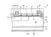
- FIG. 1 is a plan view of a semiconductor device 1 (IGBT) according to a first embodiment. It is sectional drawing which follows the II line
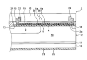
- FIG. 2 is a cross-sectional view taken along the line II-II in FIG. 3 is a schematic plan view in which a connection region between conductor portions 6, 7, 8, 9 and an overvoltage protection diode 5 is enlarged.
- FIG. It is a figure which shows an example of the electric potential of each area
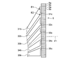
- 4 is a plan view showing a part of conductor portions 31 to 35 and an overvoltage protection diode 5 according to the embodiment. It is the top view to which the area
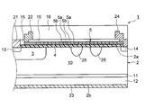
- FIG. 1 is a cross-sectional view of a semiconductor device 1 provided with two guard rings 25.
- FIG. It is a figure which shows an example of the electric potential of each area
- FIG. 6 is a cross-sectional view of a semiconductor device 1A (vertical MOSFET) according to a second embodiment. It is sectional drawing of the semiconductor device 1B (IGBT) which concerns on the modification of 1st Embodiment.
- the semiconductor device 1 according to the first embodiment is an IGBT.
- a main current flows between the upper surface 2a (one main surface) and the lower surface 2b (the other main surface) of the semiconductor substrate 2.
- the semiconductor substrate 2 is a silicon substrate in this embodiment.
- the present invention is not limited to this, and other semiconductor substrates (for example, SiC substrates, GaN substrates, etc.) may be used.
- the conductivity type of the semiconductor substrate 2 is N type in this embodiment, it is not limited to this.
- the upper surface 2a of the semiconductor substrate 2 is provided with an active region A through which a main current flows and a breakdown voltage region B surrounding the active region A.
- the breakdown voltage region B includes the peripheral edge of the semiconductor substrate 2.
- the “peripheral portion” is a peripheral portion of the semiconductor substrate 2 including the side surface of the semiconductor substrate 2.
- the insulating film 15, the surface protective film 16, the emitter electrode 21, the gate electrode 22, and the stopper electrode 24 are not shown.
- the semiconductor device 1 includes a P-type diffusion layer 3, an insulating film 4, an overvoltage protection diode 5, conductor portions 6, 7, 8, 9 and a P-type collector region. 12, an N type diffusion region 13, an N type stopper region 14, an emitter electrode 21, a gate electrode 22, a collector electrode 23, and a stopper electrode 24.
- a gate pad (not shown) is provided on the upper surface 2 a of the semiconductor substrate 2.
- the diffusion layer 3 is selectively formed on the upper surface 2 a of the breakdown voltage region B and surrounds the active region A.
- This diffusion layer 3 is also called a p-type base region. Note that a region surrounded by the boundaries P1 and P2 in FIG. 1 is a p-type base region.
- the boundary P2 is the boundary between the active region A and the withstand voltage region B.
- the depth of the diffusion layer 3 is, for example, 2 ⁇ m to 10 ⁇ m.
- the impurity concentration of the diffusion layer 3 is, for example, 1 ⁇ 10 14 cm ⁇ 3 to 1 ⁇ 10 16 cm ⁇ 3 .
- the insulating film 4 is formed on the diffusion layer 3 and the peripheral semiconductor region 10.
- the peripheral semiconductor region 10 is an N-type semiconductor region located outside the diffusion layer 3.
- the impurity concentration of the peripheral semiconductor region 10 is, for example, 1 ⁇ 10 13 cm ⁇ 3 to 1 ⁇ 10 15 cm ⁇ 3 .
- the insulating film 4 is a field oxide film, for example.
- the insulating film 4 is a silicon oxide film (SiO 2 film).
- the thickness of the insulating film 4 is, for example, 200 nm to 2000 nm.
- the overvoltage protection diode 5 has N-type semiconductor layers 5a and P-type semiconductor layers 5b that are alternately arranged adjacently on the insulating film 4 from the active region A side toward the peripheral edge of the semiconductor substrate 2.
- the overvoltage protection diode 5 is formed by connecting a plurality of Zener diodes in series.
- the diffusion region 13 is an N-type semiconductor region formed in the diffusion layer 3. As shown in FIG. 2, an emitter electrode 21 is formed on the diffusion region 13.
- the impurity concentration of the diffusion region 13 is, for example, 1 ⁇ 10 19 cm ⁇ 3 to 1 ⁇ 10 21 cm ⁇ 3 .
- the N-type stopper region 14 is formed on the upper surface 2 a at the side end of the semiconductor substrate 2.
- the impurity concentration of the stopper region 14 is higher than that of the peripheral semiconductor region 10.
- a stopper electrode 24 is formed on the stopper region 14.
- the stopper electrode 24 is electrically connected to the other end of the overvoltage protection diode 5.
- the gate electrode 22 is provided above the diffusion layer 3 with the insulating film 4 interposed therebetween.
- the gate electrode 22 is formed on the overvoltage protection diode 5 in this embodiment. More specifically, as shown in FIG. 2, the gate electrode 22 is electrically connected to one end of the overvoltage protection diode 5 on the active region A side.
- the P-type collector region 12 is formed on the lower surface 2 b of the semiconductor substrate 2.
- the impurity concentration of the collector region 12 is, for example, 1 ⁇ 10 17 cm ⁇ 3 to 1 ⁇ 10 19 cm ⁇ 3 .
- a collector electrode 23 is formed on the collector region 12.
- an N-type buffer region 11 may be provided on the collector region 12.
- the impurity concentration of the buffer region 11 is, for example, 1 ⁇ 10 16 cm ⁇ 3 to 1 ⁇ 10 18 cm ⁇ 3 .
- the semiconductor device 1 further includes an insulating film 15 that covers the overvoltage protection diode 5 and a surface protective film 16 that covers the entire upper surface 2 a side of the semiconductor device 1.
- the insulating film 15 is, for example, a BPSG (Boron Phosphorous Silicate Glass) film.
- the surface protective film 16 covers the entire upper surface 2 a side of the semiconductor substrate 2.
- the surface protective film 16 is a polyimide film, for example.
- the conductor parts 6 and 7 (first conductor part) and the conductor parts 8 and 9 (second conductor part) are formed on the insulating film 4 along the withstand voltage region B.
- the conductor portions 6, 7, 8, 9 (more precisely, the conductor constituent portions 6a, 7a, 8a, 9a) are formed in parallel to each other.
- the conductor parts 6, 7, 8, 9 are made of, for example, polysilicon or aluminum. Note that the number of conductor portions is not limited to four.
- the conductor portions 6 and 7 are disposed above the diffusion layer 3 via the insulating film 4, and the conductor portions 8 and 9 are located above the peripheral semiconductor region 10 via the insulating film 4. Is arranged.
- the conductor parts 6, 7, 8, and 9 are composed of conductor constituent parts 6a, 7a, 8a, and 9a (first conductor constituent parts) and conductor constituent parts 6b, 7b, 8b, and 9b (first conductor constituent parts). 2 conductor constituent parts) and conductor constituent parts 6c, 7c, 8c, 9c (third conductor constituent parts).
- 4 is a schematic diagram for explaining a schematic configuration of the conductor portions 6, 7, 8, and 9, and does not correspond to the plan view of FIG.
- the conductor constituent parts 6 a, 7 a, 8 a, 9 a are parts extending along the peripheral edge (side edge) of the semiconductor substrate 2 among the conductor parts 6, 7, 8, 9.
- the conductor constituent parts 6b, 7b, 8b, 9b are connected at one end to the conductor constituent parts 6a, 7a, 8a, 9a and extend to the vicinity of the overvoltage protection diode 5.
- the conductor constituent parts 6c, 7c, 8c, 9c electrically connect the conductor constituent parts 6b, 7b, 8b, 9b and the overvoltage protection diode 5.
- the conductor constituent parts 6b, 7b, 8b, 9b are formed wider than the conductor constituent parts 6a, 7a, 8a, 9a.
- the conductor constituent parts 6c, 7c, 8c, 9c are formed to be narrower than the width of the other end (end part on the overvoltage protection diode 5 side) of the conductor constituent parts 6b, 7b, 8b, 9b.
- the conductor constituent portions 6 c, 7 c, 8 c, and 9 c are provided so as to approach the pn junction boundary P 1 side between the diffusion layer 3 and the peripheral semiconductor region 10. That is, in FIG.
- the conductor constituent parts 6c and 7c are provided so as to approach the right side, and the conductor constituent parts 8c and 9c are provided so as to approach the left side. More generally, the conductor constituent portions 6c and 7c are provided so as to approach the side end side (high potential side) of the semiconductor substrate 2, and the conductor constituent portions 8c and 9c are provided on the active region A side (low side) of the semiconductor substrate 2. (Potential side).
- the collector electrode 23 is connected to a high potential (for example, the positive electrode of the DC power supply), the emitter electrode 21 is grounded, and the IGBT is not turned on to the gate electrode 22.
- a high potential for example, the positive electrode of the DC power supply
- the emitter electrode 21 is grounded
- the IGBT is not turned on to the gate electrode 22.
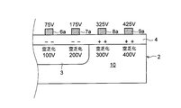
- the numerical values in FIG. 5 show an example in which a high potential of 400 V is connected to the collector electrode 23, the emitter electrode 21 is grounded, and an OFF voltage of 10 to 20 V is applied to the gate electrode 22.
- the end portions of the conductor portions 6 and 7 are electrically connected to the side surface of the overvoltage protection diode 5 so that the diffusion layer 3 in the vicinity of the insulating film 4 is depleted. Yes. More specifically, the end portions of the conductor portions 6 and 7 are side surfaces of the overvoltage protection diode 5 so that the potentials of the conductor portions 6 and 7 are higher than the potential of the diffusion layer 3 immediately below the reverse bias application state. Is electrically connected to the first portion of the. This corresponds to the conductor constituent portions 6c and 7c being provided so as to approach the pn junction boundary P1 side (that is, the high potential side).
- the end portions of the conductor portions 8 and 9 are electrically connected to the side surface of the overvoltage protection diode 5 so that the peripheral semiconductor region 10 near the insulating film 4 is depleted in the reverse bias applied state. More specifically, the end portions of the conductor portions 8 and 9 are connected to the overvoltage protection diode 5 so that the potentials of the conductor portions 8 and 9 are lower than the potential of the peripheral semiconductor region 10 immediately under the reverse bias applied state. It is electrically connected to the second part of the side surface. This corresponds to the conductor components 8c and 9c being provided so as to be closer to the pn junction boundary P1 side (that is, the low potential side).
- the P-type diffusion layer 3 in the vicinity of the insulating film 4 is depleted.
- the potential (225V) of the conductor component 7a is higher than the potential (200V) of the diffusion layer 3 immediately below the conductor component 7a, the diffusion layer 3 near the insulating film 4 is depleted. Then, a positive polarization charge is generated in the insulating film 4 by the charge of the impurity in the semiconductor region thus depleted (that is, the negative charge of the acceptor).
- the N-type peripheral semiconductor region 10 in the vicinity of the insulating film 4 is depleted.
- the potential (375 V) of the conductor component 9a is lower than the potential (400 V) of the peripheral semiconductor region 10 immediately below the conductor component 9a, the peripheral semiconductor region 10 near the insulating film 4 is depleted. Then, a negative polarization charge is generated in the insulating film 4 due to the charge of the impurity (that is, the positive charge of the donor) in the semiconductor region thus depleted.
- the semiconductor device 1 which can suppress the fall of a pressure
- the conductor parts 6 and 7 are displaced and connected to the high potential side (side end side of the semiconductor substrate 2) of the overvoltage protection diode 5 by the conductor constituent parts 6b and 7b, and the conductor parts 8 and 9 are The conductor components 8b and 9b are displaced and connected to the low potential side (active region A side) of the overvoltage protection diode 5.
- FIG. 6A five conductor portions, that is, conductor portions 31, 32, 33 (first conductor portion) and conductor portions 34, 35 (second conductor portion) are illustrated.
- the conductor portions 31, 32, 33, 34, and 35 are composed of the conductor constituent portions 31a, 32a, 33a, 34a, and 35a (first conductor constituent portions) and the conductor constituent portions 31b, 32b, 33b, 34b, and 35b (first portion). 2 conductor constituent parts) and conductor constituent parts 31c, 32c, 33c, 34c, 35c (third conductor constituent parts).
- the conductor constituent portions 31b, 32b, 33b, 34b, and 35b extend to the vicinity of the overvoltage protection diode 5 while approaching the active region A.
- the conductor constituent portions 31 b, 32 b, 33 b, 34 b, and 35 b are provided so as to approach the side end of the semiconductor substrate 2 as the distance from the overvoltage protection diode 5 increases.
- the distance between the conductor constituent portions 31a, 32a, 33a, 34a, and 35a is shortened to secure a large area of the active region A, and the depletion in the reverse bias applied state is performed as described with reference to FIG. Regions can be formed.
- the conductor constituent portions 31b, 32b, 33b, 34b, and 35b are formed so as to become thicker as they approach the overvoltage protection diode 5, as shown in FIG. 6A.
- the potential difference in the reverse bias applied state increases as the distance from the connection point with the conductor components 31c, 32c, 33c, 34c, and 35c increases in the extending direction of the overvoltage protection diode 5 (vertical direction in FIG. 6A).
- the potential difference is the difference between the potential of the conductor portions 6 and 7 and the potential of the diffusion layer 3 immediately below, or the difference between the potential of the conductor portions 8 and 9 and the potential of the peripheral semiconductor region 10 immediately below in the reverse bias applied state. That is.
- the conductor constituting portions 31c to 35c are connected to the semiconductor layer 5a or the semiconductor layer 5b of the overvoltage protection diode 5.
- the conductor constituent portions 31c to 35c are made of a semiconductor such as polysilicon
- the conductor constituent portions 31c to 35c are connected to a semiconductor layer having the same conductivity type as the semiconductor layer 5a and the semiconductor layer 5b.
- the conductor constituting portions 31c to 35c may have different conductivity types.
- the conductor portions 31, 32, 33 and / or the conductor portions 34, 35 may be connected to the overvoltage protection diode 5 so as to straddle the junction boundary between the adjacent semiconductor layers 5a and 5b. That is, the conductor portions 31 to 35 may be connected to both the adjacent semiconductor layer 5a and the semiconductor layer 5b.
- straddling the junction boundary between the adjacent semiconductor layers 5a and 5b is not limited to straddling two adjacent semiconductor layers, but three or more adjacent semiconductor layers (for example, adjacent semiconductor layers 5a, 5a, The case of straddling the semiconductor layer 5b and the semiconductor layer 5a) is also included.
- the conductor portions 31 to 35 are at least partially connected to the semiconductor layer of the same conductivity type, so that the surface layer portion of the semiconductor region located below the conductor portions 31 to 35 can be depleted. .
- a P-type guard ring 25 may be provided in the semiconductor device 1 so as to surround the diffusion layer 3 in order to increase the breakdown voltage.
- the guard ring 25 is selectively formed on the upper surface 2a of the breakdown voltage region B.
- the number of guard rings is not limited to two, and may be one or three or more.
- each semiconductor region of the semiconductor device 1 may be opposite to that described above. That is, the diffusion layer 3 may be N-type and the peripheral semiconductor region 10 may be P-type.
- the end portions of the conductor portions 6 and 7 are overvoltage protected so that the potential of the conductor portions 6 and 7 is lower than the potential of the diffusion layer 3 immediately below the reverse bias applied state. It is electrically connected to the first part on the side surface of the diode 5.
- the end portions of the conductor portions 8 and 9 are formed on the side surfaces of the overvoltage protection diode 5 so that the potentials of the conductor portions 8 and 9 are higher than the potential of the peripheral semiconductor region 10 immediately under the reverse bias applied state. It is electrically connected to the second part. This means that the conductor constituent parts 6c, 7c, 8c, 9c are provided so as to be away from the pn junction boundary P1.
- the conductor portion located above the P-type semiconductor region is electrically connected to a portion of the overvoltage protection diode 5 displaced to the high potential side, and located above the N-type semiconductor region.
- the conductor portion is electrically connected to a portion of the overvoltage protection diode 5 that is displaced to the low potential side.
- connection destination of the conductor portions 6, 7, 8, 9 to the overvoltage protection diode 5 is changed according to the conductivity type of the semiconductor layer immediately below, thereby allowing the peripheral semiconductor in the vicinity of the insulating film 4.
- the potentials of the conductor portions 6, 7, 8, and 9 are positively controlled so that the region 10 is depleted. Thereby, the movement of the movable ions of the insulating film 4 can be sufficiently suppressed.
- the configuration of the IGBT is not limited to the semiconductor device 1 described above.
- the semiconductor device 1B according to the modification has an N-type drain region 12B instead of the P-type collector region 12, and forms a Schottky barrier with the drain region 12B. It may have a collector electrode 23.
- the collector electrode 23 has a barrier metal made of platinum, molybdenum or the like.
- the semiconductor device 1A according to the second embodiment is a vertical MOSFET.
- a plan view of the semiconductor device 1A is the same as FIG.
- FIG. 9 is a cross-sectional view of the semiconductor device 1A and corresponds to FIG. 2 described in the first embodiment.
- the same components as those in the first embodiment are denoted by the same reference numerals.
- a description will be given focusing on differences from the first embodiment.
- the semiconductor device 1A includes a P-type diffusion layer 3, an insulating film 4, an overvoltage protection diode 5, conductor portions 6, 7, 8, and 9, an N-type drain region 12A, and an N-type diffusion region 13. , An N-type stopper region 14, a source electrode 21A, a gate electrode 22, a drain electrode 23A, and a stopper electrode 24.
- the drain region 12A is formed on the lower surface 2b of the semiconductor substrate 2, and the drain electrode 23A is formed on the drain region 12A. Further, the source electrode 21 ⁇ / b> A is formed on the diffusion region 13.
- the end portions of the conductor portions 6 and 7 are electrically connected to the side surface of the overvoltage protection diode 5 so that the diffusion layer 3 in the vicinity of the insulating film 4 is depleted in the reverse bias applied state.
- the end portions of the conductor portions 8 and 9 are electrically connected to the side surface of the overvoltage protection diode 5 so that the peripheral semiconductor region 10 near the insulating film 4 is depleted.
- the drain electrode 23A in the “reverse bias applied state”, the drain electrode 23A is connected to a high potential (for example, the positive electrode of a DC power supply), the source electrode 21A is grounded, and the vertical MOSFET is turned on to the gate electrode 22. This is a state in which a low voltage is applied to such an extent that it does not occur.
- the semiconductor device 1A since the same action as in the case of the first embodiment can be obtained, it is possible to provide the semiconductor device 1A that can suppress a decrease in breakdown voltage and improve reliability.
Landscapes
- Semiconductor Integrated Circuits (AREA)
- Metal-Oxide And Bipolar Metal-Oxide Semiconductor Integrated Circuits (AREA)
Abstract
Description
半導体基板の一方の主面と他方の主面との間に主電流が流れる半導体装置であって、
前記半導体基板の前記一方の主面には、活性領域と、前記活性領域を取り囲み、前記半導体基板の周縁部を含む耐圧領域とが設けられ、
前記半導体装置は、
前記耐圧領域の前記一方の主面に選択的に形成され、前記活性領域を取り囲む第2導電型の拡散層と、
前記拡散層上、および当該拡散層の外側に位置する第1導電型の周辺半導体領域上に形成された絶縁膜と、
前記活性領域側から前記半導体基板の周縁部へ向かって前記絶縁膜上に交互に隣接配置された第1導電型の半導体層と第2導電型の半導体層とを有する過電圧保護ダイオードと、
前記絶縁膜上に前記耐圧領域に沿って形成された第1の導体部および第2の導体部と、を備え、
前記第1の導体部は、前記絶縁膜を介して前記拡散層の上方に配置され、前記第2の導体部は、前記絶縁膜を介して前記周辺半導体領域の上方に配置されており、
逆バイアス印加状態において前記絶縁膜近傍の前記拡散層が空乏化するように前記第1の導体部の端部が前記過電圧保護ダイオードに電気的に接続され、および/または、前記逆バイアス印加状態において前記絶縁膜近傍の前記周辺半導体領域が空乏化するように前記第2の導体部の端部が前記過電圧保護ダイオードに電気的に接続されていることを特徴とする。
前記第1導電型がN型であり、前記第2導電型がP型であり、
前記第1の導体部の端部は、前記逆バイアス印加状態において前記第1の導体部の電位が自身の直下における前記拡散層の電位よりも高くなるように前記過電圧保護ダイオードの側面の第1の部位に電気的に接続され、
前記第2の導体部の端部は、前記逆バイアス印加状態において前記第2の導体部の電位が自身の直下における前記周辺半導体領域の電位よりも低くなるように前記過電圧保護ダイオードの前記側面の第2の部位に電気的に接続されているようにしてもよい。
前記第1の導体部は、
前記半導体基板の周縁部に沿って延在する第1の導体構成部と、
前記第1の導体構成部に一端が接続され、前記過電圧保護ダイオードの近傍まで延在する第2の導体構成部と、
前記第2の導体構成部と前記過電圧保護ダイオードを電気的に接続する第3の導体構成部と、を有し、
前記第2の導体構成部は、前記第1の導体構成部よりも幅広に形成され、
前記第3の導体構成部は、前記第2の導体構成部の他端の幅よりも幅狭に形成され、かつ前記半導体基板の側端側に寄るように設けられているようにしてもよい。
前記第2の導体部は、
前記半導体基板の周縁部に沿って延在する第1の導体構成部と、
前記第1の導体構成部に一端が接続され、前記過電圧保護ダイオードの近傍まで延在する第2の導体構成部と、
前記第2の導体構成部と前記過電圧保護ダイオードを電気的に接続する第3の導体構成部と、を有し、
前記第2の導体構成部は、前記第1の導体構成部よりも幅広に形成され、
前記第3の導体構成部は、前記第2の導体構成部の他端の幅よりも幅狭に形成され、かつ前記活性領域側に寄るように設けられているようにしてもよい。
前記第2の導体構成部は、前記過電圧保護ダイオードに近づくにつれて太くなるようにしてもよい。
前記第1導電型がP型であり、前記第2導電型がN型であり、
前記第1の導体部の端部は、前記逆バイアス印加状態において前記第1の導体部の電位が自身の直下における前記拡散層の電位よりも低くなるように前記過電圧保護ダイオードの側面の第1の部位に電気的に接続され、
前記第2の導体部の端部は、前記逆バイアス印加状態において前記第2の導体部の電位が自身の直下における前記周辺半導体領域の電位よりも高くなるように前記過電圧保護ダイオードの前記側面の第2の部位に電気的に接続されているようにしてもよい。
前記第1の導体部は、
前記半導体基板の周縁部に沿って延在する第1の導体構成部と、
前記第1の導体構成部に一端が接続され、前記過電圧保護ダイオードの近傍まで延在する第2の導体構成部と、
前記第2の導体構成部と前記過電圧保護ダイオードを電気的に接続する第3の導体構成部と、を有し、
前記第2の導体構成部は、前記第1の導体構成部よりも幅広に形成され、
前記第3の導体構成部は、前記第2の導体構成部の他端の幅よりも幅狭に形成され、かつ前記活性領域側に寄るように設けられているようにしてもよい。
前記第2の導体部は、
前記半導体基板の周縁部に沿って延在する第1の導体構成部と、
前記第1の導体構成部に一端が接続され、前記過電圧保護ダイオードの近傍まで延在する第2の導体構成部と、
前記第2の導体構成部と前記過電圧保護ダイオードを電気的に接続する第3の導体構成部と、を有し、
前記第2の導体構成部は、前記第1の導体構成部よりも幅広に形成され、
前記第3の導体構成部は、前記第2の導体構成部の他端の幅よりも幅狭に形成され、かつ前記半導体基板の側端側に寄るように設けられているようにしてもよい。
前記第2の導体構成部は、前記過電圧保護ダイオードに近づくにつれて太くなるようにしてもよい。
前記半導体基板はシリコン基板であり、前記絶縁膜はシリコン酸化膜であるようにしてもよい。
前記第1の導体部および/または前記第2の導体部は、隣接する前記第1導電型の半導体層と前記第2導電型の半導体層の接合境界を跨ぐようにして前記過電圧保護ダイオードに接続されていてもよい。
前記拡散層中に形成された第1導電型の拡散領域と、
前記拡散領域上に形成されたエミッタ電極と、
前記過電圧保護ダイオード上に形成されたゲート電極と、
前記半導体基板の前記他方の主面に形成された第2導電型のコレクタ領域と、
前記コレクタ領域上に形成されたコレクタ電極と、
をさらに備えてもよい。
前記拡散層中に形成された第1導電型の拡散領域と、
前記拡散領域上に形成されたエミッタ電極と、
前記過電圧保護ダイオード上に形成されたゲート電極と、
前記半導体基板の前記他方の主面に形成された第1導電型のドレイン領域と、
前記ドレイン領域上に形成され、前記ドレイン領域とショットキー障壁を形成するコレクタ電極と、
をさらに備えることを特徴とする請求項1~10のいずれかに記載の半導体装置。
前記拡散層中に形成された第1導電型の拡散領域と、
前記拡散領域上に形成されたソース電極と、
前記過電圧保護ダイオード上に形成されたゲート電極と、
前記半導体基板の前記他方の主面に形成された第1導電型のドレイン領域と、
前記ドレイン領域上に形成されたドレイン電極と、
をさらに備えてもよい。
前記耐圧領域の前記一方の主面に選択的に形成され、前記拡散層を取り囲む1本または複数本の第2導電型のガードリングをさらに備えてもよい。
本発明の第1の実施形態について説明する。第1の実施形態に係る半導体装置1は、IGBTである。
次に、本発明の第2の実施形態について説明する。第2の実施形態に係る半導体装置1Aは、縦型MOSFETである。半導体装置1Aの平面図は、図1と同様である。図9は、半導体装置1Aの断面図であり、第1の実施形態で説明した図2に対応する。なお、図9において、第1の実施形態と同じ構成要素には同じ符号を付している。以下、第1の実施形態との相違点を中心に説明する。
2 半導体基板
2a 上面
2b 下面
3 拡散層
4 絶縁膜
5 過電圧保護ダイオード
5a,5b 半導体層
6,7,8,9,31,32,33,34,35 導体部
6a,7a,8a,9a,6b,7b,8b,9b,6c,7c,8c,9c 導体構成部
10 周辺半導体領域
11 バッファ領域
12 コレクタ領域
12A,12B ドレイン領域
13 拡散領域
14 ストッパ領域
15 絶縁膜
16 表面保護膜
21 エミッタ電極
21A ソース電極
22 ゲート電極
23 コレクタ電極
23A ドレイン電極
24 ストッパ電極
25 ガードリング
A 活性領域
B 耐圧領域
E1,E2 端点
P1,P2 (拡散層3の)境界
R 領域
Claims (15)
- 半導体基板の一方の主面と他方の主面との間に主電流が流れる半導体装置であって、
前記半導体基板の前記一方の主面には、活性領域と、前記活性領域を取り囲み、前記半導体基板の周縁部を含む耐圧領域とが設けられ、
前記半導体装置は、
前記耐圧領域の前記一方の主面に選択的に形成され、前記活性領域を取り囲む第2導電型の拡散層と、
前記拡散層上、および当該拡散層の外側に位置する第1導電型の周辺半導体領域上に形成された絶縁膜と、
前記活性領域側から前記半導体基板の周縁部へ向かって前記絶縁膜上に交互に隣接配置された第1導電型の半導体層と第2導電型の半導体層とを有する過電圧保護ダイオードと、
前記絶縁膜上に前記耐圧領域に沿って形成された第1の導体部および第2の導体部と、を備え、
前記第1の導体部は、前記絶縁膜を介して前記拡散層の上方に配置され、前記第2の導体部は、前記絶縁膜を介して前記周辺半導体領域の上方に配置されており、
逆バイアス印加状態において前記絶縁膜近傍の前記拡散層が空乏化するように前記第1の導体部の端部が前記過電圧保護ダイオードに電気的に接続され、および/または、前記逆バイアス印加状態において前記絶縁膜近傍の前記周辺半導体領域が空乏化するように前記第2の導体部の端部が前記過電圧保護ダイオードに電気的に接続されていることを特徴とする半導体装置。 - 前記第1導電型がN型であり、前記第2導電型がP型であり、
前記第1の導体部の端部は、前記逆バイアス印加状態において前記第1の導体部の電位が自身の直下における前記拡散層の電位よりも高くなるように前記過電圧保護ダイオードの側面の第1の部位に電気的に接続され、
前記第2の導体部の端部は、前記逆バイアス印加状態において前記第2の導体部の電位が自身の直下における前記周辺半導体領域の電位よりも低くなるように前記過電圧保護ダイオードの前記側面の第2の部位に電気的に接続されていることを特徴とする請求項1に記載の半導体装置。 - 前記第1の導体部は、
前記半導体基板の周縁部に沿って延在する第1の導体構成部と、
前記第1の導体構成部に一端が接続され、前記過電圧保護ダイオードの近傍まで延在する第2の導体構成部と、
前記第2の導体構成部と前記過電圧保護ダイオードを電気的に接続する第3の導体構成部と、を有し、
前記第2の導体構成部は、前記第1の導体構成部よりも幅広に形成され、
前記第3の導体構成部は、前記第2の導体構成部の他端の幅よりも幅狭に形成され、かつ前記半導体基板の側端側に寄るように設けられていることを特徴とする請求項2に記載の半導体装置。 - 前記第2の導体部は、
前記半導体基板の周縁部に沿って延在する第1の導体構成部と、
前記第1の導体構成部に一端が接続され、前記過電圧保護ダイオードの近傍まで延在する第2の導体構成部と、
前記第2の導体構成部と前記過電圧保護ダイオードを電気的に接続する第3の導体構成部と、を有し、
前記第2の導体構成部は、前記第1の導体構成部よりも幅広に形成され、
前記第3の導体構成部は、前記第2の導体構成部の他端の幅よりも幅狭に形成され、かつ前記活性領域側に寄るように設けられていることを特徴とする請求項2に記載の半導体装置。 - 前記第2の導体構成部は、前記過電圧保護ダイオードに近づくにつれて太くなることを特徴とする請求項3または4に記載の半導体装置。
- 前記第1導電型がP型であり、前記第2導電型がN型であり、
前記第1の導体部の端部は、前記逆バイアス印加状態において前記第1の導体部の電位が自身の直下における前記拡散層の電位よりも低くなるように前記過電圧保護ダイオードの側面の第1の部位に電気的に接続され、
前記第2の導体部の端部は、前記逆バイアス印加状態において前記第2の導体部の電位が自身の直下における前記周辺半導体領域の電位よりも高くなるように前記過電圧保護ダイオードの前記側面の第2の部位に電気的に接続されていることを特徴とする請求項1に記載の半導体装置。 - 前記第1の導体部は、
前記半導体基板の周縁部に沿って延在する第1の導体構成部と、
前記第1の導体構成部に一端が接続され、前記過電圧保護ダイオードの近傍まで延在する第2の導体構成部と、
前記第2の導体構成部と前記過電圧保護ダイオードを電気的に接続する第3の導体構成部と、を有し、
前記第2の導体構成部は、前記第1の導体構成部よりも幅広に形成され、
前記第3の導体構成部は、前記第2の導体構成部の他端の幅よりも幅狭に形成され、かつ前記活性領域側に寄るように設けられていることを特徴とする請求項6に記載の半導体装置。 - 前記第2の導体部は、
前記半導体基板の周縁部に沿って延在する第1の導体構成部と、
前記第1の導体構成部に一端が接続され、前記過電圧保護ダイオードの近傍まで延在する第2の導体構成部と、
前記第2の導体構成部と前記過電圧保護ダイオードを電気的に接続する第3の導体構成部と、を有し、
前記第2の導体構成部は、前記第1の導体構成部よりも幅広に形成され、
前記第3の導体構成部は、前記第2の導体構成部の他端の幅よりも幅狭に形成され、かつ前記半導体基板の側端側に寄るように設けられていることを特徴とする請求項6に記載の半導体装置。 - 前記第2の導体構成部は、前記過電圧保護ダイオードに近づくにつれて太くなることを特徴とする請求項7または8に記載の半導体装置。
- 前記半導体基板はシリコン基板であり、前記絶縁膜はシリコン酸化膜であることを特徴とする請求項1~9のいずれかに記載の半導体装置。
- 前記第1の導体部および/または前記第2の導体部は、隣接する前記第1導電型の半導体層と前記第2導電型の半導体層の接合境界を跨ぐようにして前記過電圧保護ダイオードに接続されていることを特徴とする請求項1~10のいずれかに記載の半導体装置。
- 前記拡散層中に形成された第1導電型の拡散領域と、
前記拡散領域上に形成されたエミッタ電極と、
前記過電圧保護ダイオード上に形成されたゲート電極と、
前記半導体基板の前記他方の主面に形成された第2導電型のコレクタ領域と、
前記コレクタ領域上に形成されたコレクタ電極と、
をさらに備えることを特徴とする請求項1~11のいずれかに記載の半導体装置。 - 前記拡散層中に形成された第1導電型の拡散領域と、
前記拡散領域上に形成されたエミッタ電極と、
前記過電圧保護ダイオード上に形成されたゲート電極と、
前記半導体基板の前記他方の主面に形成された第1導電型のドレイン領域と、
前記ドレイン領域上に形成され、前記ドレイン領域とショットキー障壁を形成するコレクタ電極と、
をさらに備えることを特徴とする請求項1~11のいずれかに記載の半導体装置。 - 前記拡散層中に形成された第1導電型の拡散領域と、
前記拡散領域上に形成されたソース電極と、
前記過電圧保護ダイオード上に形成されたゲート電極と、
前記半導体基板の前記他方の主面に形成された第1導電型のドレイン領域と、
前記ドレイン領域上に形成されたドレイン電極と、
をさらに備えることを特徴とする請求項1~11のいずれかに記載の半導体装置。 - 前記耐圧領域の前記一方の主面に選択的に形成され、前記拡散層を取り囲む1本または複数本の第2導電型のガードリングをさらに備えることを特徴とする請求項1~14のいずれかに記載の半導体装置。
Priority Applications (5)
| Application Number | Priority Date | Filing Date | Title |
|---|---|---|---|
| US15/540,823 US10199483B2 (en) | 2016-05-26 | 2016-05-26 | Semiconductor device |
| PCT/JP2016/065645 WO2017203671A1 (ja) | 2016-05-26 | 2016-05-26 | 半導体装置 |
| JP2017521166A JP6258561B1 (ja) | 2016-05-26 | 2016-05-26 | 半導体装置 |
| CN201680004704.3A CN107710408B (zh) | 2016-05-26 | 2016-05-26 | 半导体装置 |
| NL2018982A NL2018982B1 (en) | 2016-05-26 | 2017-05-26 | Semiconductor device |
Applications Claiming Priority (1)
| Application Number | Priority Date | Filing Date | Title |
|---|---|---|---|
| PCT/JP2016/065645 WO2017203671A1 (ja) | 2016-05-26 | 2016-05-26 | 半導体装置 |
Publications (1)
| Publication Number | Publication Date |
|---|---|
| WO2017203671A1 true WO2017203671A1 (ja) | 2017-11-30 |
Family
ID=59683994
Family Applications (1)
| Application Number | Title | Priority Date | Filing Date |
|---|---|---|---|
| PCT/JP2016/065645 Ceased WO2017203671A1 (ja) | 2016-05-26 | 2016-05-26 | 半導体装置 |
Country Status (5)
| Country | Link |
|---|---|
| US (1) | US10199483B2 (ja) |
| JP (1) | JP6258561B1 (ja) |
| CN (1) | CN107710408B (ja) |
| NL (1) | NL2018982B1 (ja) |
| WO (1) | WO2017203671A1 (ja) |
Families Citing this family (1)
| Publication number | Priority date | Publication date | Assignee | Title |
|---|---|---|---|---|
| US10580906B1 (en) * | 2018-10-01 | 2020-03-03 | Nxp B.V. | Semiconductor device comprising a PN junction diode |
Citations (4)
| Publication number | Priority date | Publication date | Assignee | Title |
|---|---|---|---|---|
| JP2003188381A (ja) * | 2001-12-21 | 2003-07-04 | Denso Corp | 半導体装置 |
| US6762440B1 (en) * | 2000-01-18 | 2004-07-13 | Infineon Technologies Ag | Semiconductor component and corresponding test method |
| JP2005217152A (ja) * | 2004-01-29 | 2005-08-11 | Mitsubishi Electric Corp | 半導体装置 |
| JP2014187071A (ja) * | 2013-03-21 | 2014-10-02 | Shindengen Electric Mfg Co Ltd | Igbt及びigbtの製造方法 |
Family Cites Families (15)
| Publication number | Priority date | Publication date | Assignee | Title |
|---|---|---|---|---|
| DE3046749C2 (de) | 1979-12-10 | 1986-01-16 | Sharp K.K., Osaka | MOS-Transistor für hohe Betriebsspannungen |
| JPS5683076A (en) | 1979-12-10 | 1981-07-07 | Sharp Corp | High tension mos field-effect transistor |
| GB9207860D0 (en) | 1992-04-09 | 1992-05-27 | Philips Electronics Uk Ltd | A semiconductor component |
| US5589408A (en) * | 1995-07-05 | 1996-12-31 | Motorola, Inc. | Method of forming an alloyed drain field effect transistor and device formed |
| JP4140232B2 (ja) * | 2001-12-07 | 2008-08-27 | 株式会社デンソー | 半導体装置 |
| JP2004296819A (ja) | 2003-03-27 | 2004-10-21 | Shindengen Electric Mfg Co Ltd | 半導体装置 |
| JP4731816B2 (ja) * | 2004-01-26 | 2011-07-27 | 三菱電機株式会社 | 半導体装置 |
| JP4935192B2 (ja) * | 2006-05-31 | 2012-05-23 | 三菱電機株式会社 | 半導体装置 |
| JP2008177328A (ja) | 2007-01-18 | 2008-07-31 | Denso Corp | 半導体装置およびその製造方法 |
| JP5271515B2 (ja) * | 2007-07-13 | 2013-08-21 | ルネサスエレクトロニクス株式会社 | 半導体装置 |
| JP2009111304A (ja) | 2007-11-01 | 2009-05-21 | Fuji Electric Device Technology Co Ltd | 過電圧保護機能内蔵型mos型半導体装置とその製造方法。 |
| JP5182766B2 (ja) * | 2009-12-16 | 2013-04-17 | 三菱電機株式会社 | 高耐圧半導体装置 |
| US9245984B2 (en) * | 2013-01-31 | 2016-01-26 | Infineon Technologies Ag | Reverse blocking semiconductor device, semiconductor device with local emitter efficiency modification and method of manufacturing a reverse blocking semiconductor device |
| CN104981903B (zh) * | 2013-03-14 | 2017-12-01 | 富士电机株式会社 | 半导体装置 |
| JP6649102B2 (ja) * | 2016-02-05 | 2020-02-19 | ルネサスエレクトロニクス株式会社 | 半導体装置 |
-
2016
- 2016-05-26 CN CN201680004704.3A patent/CN107710408B/zh active Active
- 2016-05-26 US US15/540,823 patent/US10199483B2/en active Active
- 2016-05-26 WO PCT/JP2016/065645 patent/WO2017203671A1/ja not_active Ceased
- 2016-05-26 JP JP2017521166A patent/JP6258561B1/ja active Active
-
2017
- 2017-05-26 NL NL2018982A patent/NL2018982B1/nl active
Patent Citations (4)
| Publication number | Priority date | Publication date | Assignee | Title |
|---|---|---|---|---|
| US6762440B1 (en) * | 2000-01-18 | 2004-07-13 | Infineon Technologies Ag | Semiconductor component and corresponding test method |
| JP2003188381A (ja) * | 2001-12-21 | 2003-07-04 | Denso Corp | 半導体装置 |
| JP2005217152A (ja) * | 2004-01-29 | 2005-08-11 | Mitsubishi Electric Corp | 半導体装置 |
| JP2014187071A (ja) * | 2013-03-21 | 2014-10-02 | Shindengen Electric Mfg Co Ltd | Igbt及びigbtの製造方法 |
Also Published As
| Publication number | Publication date |
|---|---|
| NL2018982A (en) | 2017-11-27 |
| NL2018982B1 (en) | 2018-02-16 |
| JPWO2017203671A1 (ja) | 2018-06-07 |
| CN107710408B (zh) | 2021-06-18 |
| US20180204935A1 (en) | 2018-07-19 |
| JP6258561B1 (ja) | 2018-01-10 |
| CN107710408A (zh) | 2018-02-16 |
| US10199483B2 (en) | 2019-02-05 |
Similar Documents
| Publication | Publication Date | Title |
|---|---|---|
| JP5477681B2 (ja) | 半導体装置 | |
| JP6392133B2 (ja) | 半導体装置 | |
| JP5517688B2 (ja) | 半導体装置 | |
| JP5863574B2 (ja) | 半導体装置 | |
| CN101350365B (zh) | 半导体器件 | |
| JP5048273B2 (ja) | 絶縁ゲート型半導体装置 | |
| JP6739372B2 (ja) | 半導体装置 | |
| JP5701913B2 (ja) | 半導体装置 | |
| US10276654B2 (en) | Semiconductor device with parallel PN structures | |
| JP2013149761A (ja) | 半導体装置 | |
| TWI416732B (zh) | Semiconductor device | |
| JP5694285B2 (ja) | 半導体装置 | |
| JP6258561B1 (ja) | 半導体装置 | |
| JP6408405B2 (ja) | 半導体装置 | |
| JP6224291B1 (ja) | 半導体装置 | |
| JP6301551B1 (ja) | 半導体装置 | |
| JP5774744B2 (ja) | 半導体装置 | |
| JP6058712B2 (ja) | 半導体装置 | |
| JP7404601B2 (ja) | 半導体集積回路 | |
| JP2023136028A (ja) | 半導体装置 | |
| JP2016187006A (ja) | 半導体装置 |
Legal Events
| Date | Code | Title | Description |
|---|---|---|---|
| ENP | Entry into the national phase |
Ref document number: 2017521166 Country of ref document: JP Kind code of ref document: A |
|
| WWE | Wipo information: entry into national phase |
Ref document number: 15540823 Country of ref document: US |
|
| NENP | Non-entry into the national phase |
Ref country code: DE |
|
| 121 | Ep: the epo has been informed by wipo that ep was designated in this application |
Ref document number: 16903152 Country of ref document: EP Kind code of ref document: A1 |
|
| 122 | Ep: pct application non-entry in european phase |
Ref document number: 16903152 Country of ref document: EP Kind code of ref document: A1 |