WO2017199937A1 - 電気部品用ソケット - Google Patents
電気部品用ソケット Download PDFInfo
- Publication number
- WO2017199937A1 WO2017199937A1 PCT/JP2017/018318 JP2017018318W WO2017199937A1 WO 2017199937 A1 WO2017199937 A1 WO 2017199937A1 JP 2017018318 W JP2017018318 W JP 2017018318W WO 2017199937 A1 WO2017199937 A1 WO 2017199937A1
- Authority
- WO
- WIPO (PCT)
- Prior art keywords
- pressing member
- pressing
- socket
- cam
- electrical component
- Prior art date
- Legal status (The legal status is an assumption and is not a legal conclusion. Google has not performed a legal analysis and makes no representation as to the accuracy of the status listed.)
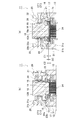
- Ceased
Links
Images







Classifications
-
- H—ELECTRICITY
- H01—ELECTRIC ELEMENTS
- H01R—ELECTRICALLY-CONDUCTIVE CONNECTIONS; STRUCTURAL ASSOCIATIONS OF A PLURALITY OF MUTUALLY-INSULATED ELECTRICAL CONNECTING ELEMENTS; COUPLING DEVICES; CURRENT COLLECTORS
- H01R33/00—Coupling devices specially adapted for supporting apparatus and having one part acting as a holder providing support and electrical connection via a counterpart which is structurally associated with the apparatus, e.g. lamp holders; Separate parts thereof
- H01R33/74—Devices having four or more poles, e.g. holders for compact fluorescent lamps
- H01R33/76—Holders with sockets, clips, or analogous contacts adapted for axially-sliding engagement with parallely-arranged pins, blades, or analogous contacts on counterpart, e.g. electronic tube socket
Definitions
- the present invention relates to an electrical component socket for evaluating, for example, an electrical component such as an IC package detachably accommodated in a socket body and electrically connected to a wiring board.
- a socket body having a housing portion in which an IC package is detachably accommodated, a socket cover that is pivotally attached to the socket body and opens and closes the housing portion, and can be moved up and down on the socket cover And a lever member that pushes down the heat dissipation member and presses the IC package with a predetermined contact pressure has been proposed (for example, see Patent Document 1).
- this IC socket cannot support other IC packages with different thicknesses. Furthermore, in this IC socket, even if the thickness of one of the pressed locations is changed in an IC package with specifications having two pressed locations with different thicknesses (for example, a stepped IC package). There was a problem that it was not possible to cope with it.
- the present invention can appropriately evaluate two types of electrical components such as IC packages having different thicknesses, and can cope with a change in the thickness of an electrical component such as an IC package having two pressed locations.
- An object of the present invention is to provide a socket for electric parts that can be used.
- the present invention provides a socket body having a housing portion in which an electrical component is detachably accommodated, and a socket that is rotatably provided in the socket body so as to open and close the housing portion.
- an outer pressing member that is provided on the outer side so as to be movable up and down independently of the inner pressing member, and that presses the electrical component or the socket main body accommodated in the accommodating portion of the socket main body, and pivots on the socket cover When a first pressing portion that is freely provided and is rotated in one direction to press down the inner pressing member and the outer pressing member is formed.
- the electrical component socket includes a cam formed with a second pressing portion that presses down the inner pressing member and the outer pressing member by rotating in the other direction, and a bale that rotates the cam.
- the cam includes a first inner cam portion that contacts the inner pressing member and presses the inner pressing member, and a first inner pressing member that presses the outer pressing member and presses the outer pressing member.
- One outer cam portion is an electrical component socket formed so as to form a first step.
- the second pressing portion of the cam contacts the inner pressing member to push down the inner pressing member, and the second inner cam portion presses the outer pressing member to press down the outer pressing member. It is desirable that the two outer cam portions be formed so as not to cause a step.
- the second pressing portion of the cam is in contact with the inner pressing member and presses the inner pressing member, and the outer pressing member is in contact with the outer pressing member. It is desirable that the second outer cam portion that pushes down is formed so as to produce a second step that is smaller than the first step.
- the cam when the first electrical component as the electrical component is accommodated in the accommodating portion of the socket body, the cam is rotated in the one direction, and the first pressing portion is the first inner side.
- the first electric component is pressed from above by pressing down the inner pressing member with a cam portion, and the socket body is pressed from above by pressing down the outer pressing member with the first outer cam portion.
- the cam is rotated in the other direction, and the second pressing portion Presses the second electrical component from above by pressing down the inner pressing member with the second inner cam portion, and pressing down the outer pressing member with the second outer cam portion. Pressing the socket body from above, so it is desirable configuration.
- the cam when the stepped third electrical component as the electrical component is accommodated in the accommodating portion of the socket body, the cam is rotated in the one direction, and the first pressing The upper portion of the third electric component is pressed from above by pressing down the inner pressing member with the first inner cam portion, and the third pressing portion is pressed down with the first outer cam portion.
- the bale has a substantially U-shape, and a pair of cams are attached to both ends of the bail, and the pair of cams is operated by operating the bail. It is desirable that is configured to be rotatable.
- the cam is detachably attached to the bale.
- the cam is formed in the first pressing portion or the second pressing portion so that a step is formed between the inner cam portion for pressing the inner pressing member and the outer cam portion for pressing the outer pressing member. Therefore, the inner pressing member is pushed down by the inner cam portion, and the outer pressing member is pushed down by the outer cam portion, whereby the inner pressing member and the outer pressing member can be moved up and down independently. As a result, it is possible to appropriately evaluate two types of electrical components having different thicknesses, or to provide an electrical component socket that can cope with a step difference between electrical components having two pressed locations. it can.
- the pair of cams can be rotated by operating the substantially U-shaped bale, it is possible to easily perform the pressing operation of the inner pressing member and the outer pressing member, and thus the evaluation of the electrical component. It becomes.
- the cam detachably with respect to the bale by providing the cam detachably with respect to the bale, it is possible to cope with a change in the thickness of the electrical component by simply replacing the cam, and the convenience of the socket for the electrical component can be improved. It becomes.
- the present invention by providing a heat sink on the inner pressing member, it is possible to dissipate heat generated in the electrical component along with the evaluation of the electrical component. Accordingly, it is possible to prevent malfunction due to heat generation of the electrical component, and to continue the evaluation of the electrical component smoothly.
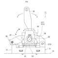
- FIG. 6 is a plan view showing a state where the inner pressing member is not pressing the IC package in the IC socket according to the first embodiment of the present invention.
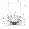
- the IC socket which concerns on Embodiment 1 of this invention it is a front view which shows the state which the inner side press member is not pressing the IC package.
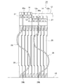
- FIG. 2 is a cross-sectional view taken along line AA in FIG. It is sectional drawing which shows the contact module of the IC socket which concerns on the same Embodiment 1, Comprising: The left half is the state figure which the floating plate raised, The right half is the state figure which the floating plate fell. It is the perspective view which looked at the cam of the IC socket which concerns on the same Embodiment 1 from inner side diagonally downward.
- FIG. 6 is a plan view showing a state where the inner pressing member is pressing a thick IC package in the IC socket according to the first embodiment.
- FIG. 8 is a cross-sectional view taken along line BB in FIG.
- FIG. 8 is a cross-sectional view taken along the line CC of FIG.
- FIG. 8 is a cross-sectional view taken along line DD in FIG. 7.
- FIG. 12 is a cross-sectional view taken along line EE in FIG. 11. It is sectional drawing which follows the FF line
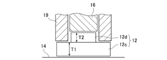
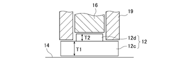
- IC socket concerning Embodiment 2 of this invention it is sectional drawing which shows a mode that a stepped IC package is evaluated, Comprising: It is a figure of the state which presses the thick IC package.
- IC socket concerning Embodiment 2 of this invention it is sectional drawing which shows a mode that an IC package with a step is evaluated, Comprising: It is a figure of the state which is pressing the IC package with a thin upper part.
- Embodiment 1 of the Invention 1 to 15 show a first embodiment of the present invention.
- the clamshell type IC socket 11 as the “electrical component socket” according to the first embodiment is arranged on the wiring board 13 as shown in FIG. 1 to FIG.
- an electrical connection between the spherical terminal 12a of the IC package 12 and the wiring board 13 is intended.
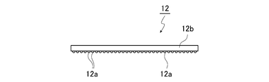
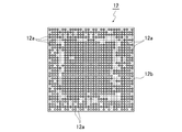
- the IC package 12 is called a ball grid array (BGA). As shown in FIGS. 6A and 6B, the IC package 12 has a rectangular package body 12b in plan view, and on the lower surface of the package body 12b, A plurality of spherical terminals 12a are arranged in a lattice shape and formed so as to protrude downward.
- BGA ball grid array
- the IC socket 11 generally includes a socket body 31, an inner pressing member 16, an outer pressing member 19, a pair of cams 20, And a veil (lever) 25 having a letter shape.
- the socket body 31 includes a substantially square frame 15 and a contact module 24 incorporated in the central cavity of the frame 15. Yes.
- the contact module 24 is for housing the IC package 12.
- the contact module 24 includes a module main body 28, a plurality of substantially S-shaped contact pins 26, and a substantially flat floating plate 27. It is configured.
- a plurality of substantially S-shaped contact pins 26 are arranged on the module main body 28 so as to be extendable in the vertical direction.
- a substantially flat floating plate 27 is always elastically urged upward by a biasing means (not shown) such as a coil spring above the module main body 28, with respect to the module main body 28. It is arranged to be movable up and down by a predetermined stroke L1.
- a biasing means such as a coil spring
- a substantially square frame-shaped guide member (hard stop) 17 is attached to the socket body 31 so as to surround the accommodating portion 14.
- a socket cover 29 is attached to the upper side of the socket body 31 so as to open and close the accommodating portion 14 so as to rotate in the directions of arrows M and N about the rotation axis CT2.
- biasing means such as a torsion coil spring is disposed so as to elastically bias the socket cover 29 in the direction of arrow M at all times.
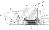
- a latch member 30 is attached to the distal end portion of the socket cover 29, and the latch member 30 hooks its locking claw 30 a on the locked step portion 15 a of the frame body 15. By being locked, the closed state of the socket cover 29 can be maintained.
- a substantially rectangular parallelepiped inner pressing member 16 that presses 12 (12A, 12B) is always movable upward and downward by a biasing means (not shown) such as a coil spring.
- the outer pressing member 19 having a substantially square frame plate shape that presses the guide member 17 of the socket body 31 is provided on the outer periphery of the inner pressing member 16 and biasing means (not shown) such as a coil spring. Therefore, it is supported so as to be movable up and down independently of the inner pressing member 16 in such a manner that it is always urged upward.
- a heat sink 18 is integrally provided on the upper side of the inner pressing member 16.
- a substantially U-shaped bail 25 is rotatable in the forward and reverse directions (in the directions of arrows I and J) about the rotation axis CT3 as shown in FIGS.
- One cam 20 is detachably attached to both tip portions of the bail 25. Then, by rotating the bail 25, the pair of cams 20 is configured to be rotatable in forward and reverse directions (arrows K and L directions) about the rotation axis CT1.
- the rotation axis CT1 of the pair of cams 20 coincides with the rotation axis CT3 of the bail 25, and the directions of arrows K and L coincide with the directions of arrows I and J, respectively.
- the pair of cams 20 are arranged symmetrically so as to face each other with the inner pressing member 16 interposed therebetween.
- the first pressing portion 21 of the cam 20 contacts the inner pressing member 16 when the bail 25 is positioned at the first pressing position P1 (see FIG. 8).
- An inner cam portion 21a that presses down the inner pressing member 16 (corresponding to the “first inner cam portion” of the present invention) and an outer cam portion 21b that contacts the outer pressing member 19 and presses down the outer pressing member 19 (“ Corresponding to the “second inner cam portion”) are formed so as to form a step (corresponding to the “first step” of the present invention).
- the second pressing portion 22 of the cam 20 contacts the inner pressing member 16 when the bail 25 is positioned at the second pressing position P2 (see FIG. 12).
- the inner cam portion 22a (corresponding to the “second inner cam portion” of the present invention) that pushes down the inner pressing member 16 and the outer cam portion 22b that touches the outer pressing member 19 and pushes down the outer pressing member 19 (“ Corresponding to the “second outer cam portion”) are formed so as not to produce a step difference (that is, in the same cam shape).
- the cam 20 has a distance D11 from the center of the rotating shaft CT1 to the contact surface of the inner cam portion 21a of the first pressing portion 21 so that the outer cam of the first pressing portion 21 from the center of the rotating shaft CT1. Since this distance is shorter than the distance D12 to the contact surface of the part 21b (that is, D11 ⁇ D12, see FIGS. 5A and 5B), the gap C1 corresponds to a thick IC package 12A described later.
- the bail 25 is on standby.
- the inner pressing member 16 and the outer pressing member 19 can be evenly pressed down without being inclined when positioned at any of the position P3, the first pressing position P1, and the second pressing position P2.
- the bail 25 is appropriately operated according to the thickness of the IC package 12 as described below. By doing so, two types of IC packages 12 (thick IC package 12A and thin IC package 12B) having different thicknesses can be properly evaluated.
- the socket cover 29 When evaluating the thick IC package 12A (corresponding to the “first electrical component” of the present invention), the socket cover 29 is opened after the IC socket 11 is disposed on the wiring board 13 as shown in FIG. In this state, the thick IC package 12A is accommodated in the accommodating portion 14 of the socket body 31 and is seated. Next, the socket cover 29 is closed by rotating in the direction of arrow N about the rotation axis CT2, and the closed state is held by the latch member 30, and then the bail 25 is rotated in the direction of arrow I about the rotation axis CT3. Then, positioning is performed from the standby position P3 to the first pressing position P1 (see FIG. 9). Then, the inner pressing member 16 is pushed by the inner cam portion 21a of the first pressing portion 21 of the cam 20 and descends by a predetermined distance.
- the thick IC package 12A can be properly evaluated by passing a current through the IC package 12A and performing a burn-in test or the like.
- the outer pressing member 19 is pushed down by the outer cam portion 21b of the first pressing portion 21 of the cam 20, and comes into contact with the frame body 15 of the socket body 31 and the upper surface of the guide member 17, as shown in FIG. And is in a positioned state.
- the socket cover 29 is provided. Is opened, the thin IC package 12B is accommodated in the accommodating portion 14 of the socket body 31 and seated. Next, the socket cover 29 is closed by rotating in the direction of arrow N about the rotation axis CT2, and the closed state is held by the latch member 30, and then the bail 25 is rotated in the direction of arrow J about the rotation axis CT3. Then, positioning is performed from the standby position P3 to the second pressing position P2 (see FIG. 13). Then, the inner pressing member 16 is pushed by the inner cam portion 22a of the second pressing portion 22 of the cam 20 and is lowered by a predetermined distance.
- the floating plate 27 is pushed down by the inner pressing member 16, and all the contact pins 26 bend. Therefore, the upper contact portions 26a of the contact pins 26 are respectively connected to the IC package 12B. While contacting the spherical terminal 12a, the lower contact portion 26b of each contact pin 26 contacts the wiring board 13 with a predetermined contact pressure.
- the gap C2 corresponding to the thin IC package 12B is formed between the pressing surface 16a of the inner pressing member 16 and the accommodating portion 14 before the IC package 12B is accommodated in the accommodating portion 14, as described above. Since this occurs, the amount of lowering of the floating plate 27, and hence the amount of deflection of the contact pin 26, matches the specified value. As a result, in this state, the thin IC package 12B can be properly evaluated by passing a current through the IC package 12B and performing a burn-in test or the like.
- the outer pressing member 19 is pushed down by the outer cam portion 22b of the second pressing portion 22 of the cam 20, and comes into contact with the frame body 15 of the socket body 31 and the upper surface of the guide member 17, as shown in FIG. And is in a positioned state.
- the inner pressing member 16 and the outer pressing member 19 are in a predetermined positional relationship (vertical direction). Regardless of the thickness, the pressing amount of the IC package 12 can be set to a predetermined pressing amount.
- the pair of cams 20 can be rotated by operating the substantially U-shaped bail 25. Therefore, the pressing operation of the inner pressing member 16 and the outer pressing member 19, As a result, the evaluation of the IC package 12 can be easily performed.
- the pair of cams 20 are provided detachably with respect to the bail 25, so that by simply replacing these cams 20, three or more types of IC packages 12 can be obtained.
- the thickness can also be accommodated. As a result, the convenience of the IC socket 11 can be improved.
- FIG. 16A and 16B show Embodiment 2 of the present invention.
- the basic configuration of the IC socket 11 is the same as in the first embodiment described above, and the objects to be pressed by the inner pressing member 16 and the outer pressing member 19 are different.
- the upper portion 12d of the IC package 12 is pressed by the inner pressing member 16, and the base portion 12c of the IC package 12 is also measured.
- the evaluation of the IC package 12 can be properly executed while suppressing the warpage of the IC package 12.
- the IC packages 12 having different thicknesses T1 of the base portion 12c or thicknesses T2 of the upper portion 12d can be accommodated.
- the thickness T1 of the base portion 12c of the IC package 12 (corresponding to “third electrical component” of the present invention) is the same
- the thickness T2 of the upper portion 12d of the IC package 12 is thick as shown in FIG. 16A.
- the first pressing portion 21 of the cam 20 is made to have the thickness T1 and the upper portion 12d of the base portion 12c so that the outer pressing member 19 and the inner pressing member 16 can appropriately press the base portion 12c and the upper portion 12d of the IC package 12, respectively.
- the thickness T2 Corresponding to the thickness T2.
- the base part 12c and the upper part 12d of the IC package 12 are The second pressing portion 22 of the cam 20 is made to correspond to the thickness T1 of the base portion 12c and the thickness T2 of the upper portion 12d so that the outer pressing member 19 and the inner pressing member 16 can be pressed appropriately. Thereby, it becomes possible to cope with the difference in thickness of the stepped IC package 12 having two pressed locations (the base portion 12c and the upper portion 12d).
- the step between the inner cam portion 21a and the outer cam portion 21b (corresponding to the “first step” in the present invention) is increased, and in the second pressing portion 22, the inner cam portion 22a and the outer cam portion.
- step difference it respond
- the dimensional relationship of each part of the cam 20 can be changed as appropriate according to the situation such as the difference in thickness between the two types of IC packages 12 and the positional relationship between the inner pressing member 16 and the outer pressing member 19.
- the IC socket 11 having the substantially S-shaped contact pin 26 has been described.
- the type of the contact pin 26 is not limited to this, and other shapes / structures (for example, an arcuate contact pin, a double-end sliding type or a single-end sliding type contact pin, etc.) can be substituted.
- the clamshell type IC socket 11 has been described.
- the present invention is similarly applied to an IC socket of a type other than the clamshell type (for example, a so-called open top type). can do.
- an IC socket in which a pair of cams 20 are attached to both tips of the substantially U-shaped bail 25 so that the inner pressing member 16 and the outer pressing member 19 can be pressed down evenly. 11 has been described.
- the number of the cams 20 is not limited to two (a pair) as long as the inner pressing member 16 and the outer pressing member 19 can be uniformly pushed down by the cam 20.
- the IC socket 11 in which the heat sink 18 is integrally provided on the inner pressing member 16 has been described.
- the heat sink 18 is not necessarily provided integrally with the inner pressing member 16, and the heat sink 18 can be omitted when the IC package 12 generates a small amount of heat.
- the stepped IC package 12 has been described as an example of the IC package 12 having the specification having two pressed locations.
- the embodiment is not limited to the stepped IC package 12, and the pressed location is not limited. It goes without saying that the present invention can be widely applied to IC packages having two specifications.
- the present invention is applied to the IC socket 11 as the “socket for electrical parts”, it is needless to say that the present invention is not limited to this and can be applied to other devices.
Landscapes
- Testing Of Individual Semiconductor Devices (AREA)
- Connecting Device With Holders (AREA)
Abstract
【課題】電気部品用ソケットにおいて、厚さが異なる2種類の電気部品を適正に評価できるようにする。 【解決手段】この電気部品用ソケットは、ソケット本体の収容部に収容された電気部品を押圧する上下動自在な内側押圧部材を有している。また、内側押圧部材と独立して上下動自在に設けられて、ソケット本体の収容部に収容された電気部品またはソケット本体を押圧する外側押圧部材を有している。さらに、一方向に回動させることにより、内側押圧部材および外側押圧部材を押し下げる第1押圧部が形成されているとともに、他方向に回動させることにより、内側押圧部材および外側押圧部材を押し下げる第2押圧部が形成されている回動自在のカムを有している。カムの第1押圧部には、内側押圧部材を押し下げる内側カム部と外側押圧部材を押し下げる外側カム部とが互いに段差を生じるように形成されている。
Description
本発明は、例えば、ICパッケージ等の電気部品を、ソケット本体に着脱自在に収容して、配線基板に電気的に接続された状態で評価するための、電気部品用ソケットに関するものである。
従来から、この種の「電気部品用ソケット」の一例として、「電気部品」であるICパッケージを着脱自在に収容するICソケットがある。
このICソケットとしては、ICパッケージが着脱自在に収容される収容部を有するソケット本体と、このソケット本体に回動自在に取り付けられて収容部を開閉するソケットカバーと、このソケットカバーに上下動自在に設けられた放熱部材と、この放熱部材を押し下げてICパッケージを所定の接圧で押圧するレバー部材を備えたものが提案されている(例えば、特許文献1参照)。
このような従来のICソケットにあっては、ソケットカバーが回動されてソケット本体の収容部が閉じられた後、レバー部材によって放熱部材が押し下げられた状態では、この放熱部材と収容部との隙間の幅(上下方向の距離)が常に一定である。そのため、ソケット本体の収容部に収容するICパッケージの厚さが一定でない場合、厚さ調整用の部材を別途使用するか、或いはICソケットを交換するか等の対策を講じない限り、そのICパッケージを所定の接圧で押圧して適正に評価することができない。
したがって、このICソケットでは、厚さが異なる別のICパッケージに対応できない。さらに、このICソケットでは、厚さの異なる2個所の押圧箇所がある仕様のICパッケージ(例えば、段付きのICパッケージなど)において、いずれか1箇所の押圧箇所の厚さが変更された場合でも、それに対応できないという課題があった。
そこで、本発明は、厚さが異なる2種類のICパッケージ等の電気部品を適正に評価することができるとともに、押圧箇所が2箇所あるICパッケージ等の電気部品の厚さ変更にも対応することが可能な電気部品用ソケットを提供することを課題としている。
かかる課題を達成するために、本発明は、電気部品が着脱自在に収容される収容部を有するソケット本体と、このソケット本体に前記収容部を開閉するように回動自在に設けられているソケットカバーと、このソケットカバーに上下動自在に設けられて、前記ソケット本体の前記収容部に収容された前記電気部品を押圧する上下動自在な内側押圧部材と、前記ソケットカバーに前記内側押圧部材より外側で当該内側押圧部材と独立して上下動自在に設けられて、前記ソケット本体の前記収容部に収容された前記電気部品または前記ソケット本体を押圧する外側押圧部材と、前記ソケットカバーに回動自在に設けられて、一方向に回動させることにより、前記内側押圧部材および前記外側押圧部材を押し下げる第1押圧部が形成されているとともに、他方向に回動させることにより、前記内側押圧部材および前記外側押圧部材を押し下げる第2押圧部が形成されているカムと、このカムを回転させるベールとを有する電気部品用ソケットであって、前記カムには、前記第1押圧部に、前記内側押圧部材に接触して当該内側押圧部材を押し下げる第1内側カム部と、前記外側押圧部材に接触して当該外側押圧部材を押し下げる第1外側カム部とが、第1段差を生じるように形成されている電気部品用ソケットとしたことを特徴とする。
本発明において、前記カムの前記第2押圧部に、前記内側押圧部材に接触して当該内側押圧部材を押し下げる第2内側カム部と、前記外側押圧部材に接触して当該外側押圧部材を押し下げる第2外側カム部とが、段差を生じないように形成されていることが望ましい。
或いは、本発明においては、前記カムの前記第2押圧部に、前記内側押圧部材に接触して当該内側押圧部材を押し下げる第2内側カム部と、前記外側押圧部材に接触して当該外側押圧部材を押し下げる第2外側カム部とが、前記第1の段差よりも小さい第2段差を生じるように形成されていることが望ましい。
本発明は、前記電気部品としての第1電気部品が前記ソケット本体の前記収容部に収容された場合に、前記カムが前記一方向に回動されて、前記第1押圧部が前記第1内側カム部で前記内側押圧部材を押し下げることにより前記第1電気部品を上方から押圧すると共に、前記第1外側カム部で前記外側押圧部材を押し下げることにより前記ソケット本体を上方から押圧し、前記電気部品としての、前記第1電気部品よりも厚さが小さい第2電気部品が前記ソケット本体の前記収容部に収容された場合に、前記カムが前記他方向に回動されて、前記第2押圧部が前記第2内側カム部で前記内側押圧部材を押し下げることにより前記第2電気部品を上方から押圧すると共に、前記第2外側カム部で前記外側押圧部材を押し下げることにより前記ソケット本体を上方から押圧する、ように構成されることが望ましい。
また、本発明は、前記電気部品としての、段付の第3電気部品が前記ソケット本体の前記収容部に収容された場合に、前記カムが前記一方向に回動されて、前記第1押圧部が前記第1内側カム部で前記内側押圧部材を押し下げることにより前記第3電気部品の上段部を上方から押圧すると共に、前記第1外側カム部で前記外側押圧部材を押し下げることにより前記第3電気部品の下段部を上方から押圧し、前記電気部品としての、前記第3電気部品よりも段差が小さい段付の第4電気部品が前記ソケット本体の前記収容部に収容された場合に、前記カムが前記他方向に回動されて、前記第2押圧部が前記第2内側カム部で前記内側押圧部材を押し下げることにより前記第4電気部品の上段部を上方から押圧すると共に、前記第2外側カム部で前記外側押圧部材を押し下げることにより前記第4電気部品の下段部上方から押圧する、ように構成されることが望ましい。
本発明においては、前記ベールは略コ字形を呈しているとともに、このベールの両方の先端部に前記カムが1個ずつ計一対取り付けられており、前記ベールを操作することにより、前記一対のカムが回転可能に構成されていることが望ましい。
本発明において、前記カムは、前記ベールに対して着脱自在に設けられていることが望ましい。
本発明においては、前記内側押圧部材にヒートシンクが設けられていることが望ましい。
本発明によれば、カムは、その第1押圧部または第2押圧部に、内側押圧部材を押し下げる内側カム部と外側押圧部材を押し下げる外側カム部とが互いに段差を生じるように形成されているので、内側カム部で内側押圧部材を押し下げるとともに、外側カム部で外側押圧部材を押し下げることにより、内側押圧部材と外側押圧部材とを独立して上下動させることが可能となる。その結果、厚さが異なる2種類の電気部品を適正に評価することができ、或いは、押圧箇所が2箇所ある電気部品の段差にも対応することが可能な電気部品用ソケットを提供することができる。
本発明において、略コ字形のベールを操作することにより、一対のカムを回転させることができるので、内側押圧部材および外側押圧部材の押下動作、ひいては電気部品の評価を容易に実行することが可能となる。
本発明において、カムをベールに対して着脱自在に設けることにより、カムを適宜交換するだけで、電気部品の厚さ変更に対応することができ、電気部品用ソケットの利便性を高めることが可能となる。
本発明において、内側押圧部材にヒートシンクが設けられることにより、電気部品の評価に伴って電気部品で発生する熱を放散することができる。したがって、電気部品の発熱による誤動作を未然に防止して、電気部品の評価を円滑に継続することが可能となる。
以下、本発明の実施形態について説明する。
[発明の実施の形態1]
図1乃至図15には、本発明の実施形態1を示す。
図1乃至図15には、本発明の実施形態1を示す。
実施形態1に係る「電気部品用ソケット」としてのクラムシェルタイプのICソケット11は、図1乃至図4に示すように、配線基板13上に配設されるようになっており、「電気部品」であるICパッケージ12等のバーンイン試験等を行うために、このICパッケージ12の球状端子12aとその配線基板13との電気的接続を図るものである。
このICパッケージ12は、ボールグリッドアレイ(BGA)と称されるもので、図6Aおよび図6Bに示すように、平面視で方形状のパッケージ本体12bを有し、このパッケージ本体12bの下面に、複数の球状端子12aが格子状に配列されて下向きに突出する形で形成されている。
また、ICソケット11は、大略、図1乃至図3、図10、図14に示すように、ソケット本体31と、内側押圧部材16と、外側押圧部材19と、一対のカム20と、略コ字形のベール(レバー)25とを有している。
さらに詳しく述べると、ソケット本体31は、図1乃至図3に示すように、略正方形枠状の枠体15と、この枠体15の中央空洞部に組み込まれたコンタクトモジュール24とから構成されている。このコンタクトモジュール24は、ICパッケージ12を収容するためのものであり、図4に示すように、モジュール本体28と、複数の略S字形のコンタクトピン26と、略平板状のフローティングプレート27とから構成されている。ここで、モジュール本体28には、複数の略S字形のコンタクトピン26が上下方向に伸縮自在に配設されている。また、モジュール本体28の上方には略平板状のフローティングプレート27が、コイルスプリング等の付勢手段(図示せず)によって常に上方に弾性的に付勢された形で、モジュール本体28に対して所定のストロークL1だけ上下動自在に配置されている。このフローティングプレート27の上部には、ICパッケージ12が着脱自在に収容される収容部14が形成されている。
さらに、ソケット本体31には、図8および図10に示すように、略正方形枠状のガイド部材(ハードストップ)17が収容部14を包囲するように取り付けられている。
また、ソケット本体31の上側には、図2に示すように、ソケットカバー29が回転軸CT2を中心として矢印M、N方向に回動する形で収容部14を開閉するように取り付けられており、ソケットカバー29とソケット本体31との間には、ねじりコイルばね等の付勢手段(図示せず)がソケットカバー29を常に矢印M方向に弾性的に付勢するように配設されている。ソケットカバー29の先端部には、図8に示すように、ラッチ部材30が取り付けられており、このラッチ部材30は、その係止爪30aを枠体15の被係止段部15aに引っ掛けて係止することにより、ソケットカバー29の閉状態を保持することができるように構成されている。
また、ソケットカバー29の略中央部には、図10、14および15に示すように、このソケットカバー29が閉状態に保持された状態で、ソケット本体31の収容部14に収容されたICパッケージ12(12A、12B)を押圧する略直方体状の内側押圧部材16が、コイルスプリング等の付勢手段(図示せず)によって常に上方(図15左方)に付勢された形で上下動自在に支持されているとともに、この内側押圧部材16の外周に、ソケット本体31のガイド部材17を押圧する略正方形枠板状の外側押圧部材19が、コイルスプリング等の付勢手段(図示せず)によって常に上方に付勢された形で内側押圧部材16と独立して上下動自在に支持されている。なお、内側押圧部材16の上側には、ヒートシンク18が一体に設けられている。
さらに、ソケットカバー29の略中央部には、図1および図2に示すように、略コ字形のベール25が回転軸CT3を中心として正逆方向(矢印I、J方向)に回動自在に設けられており、ベール25の両方の先端部にはカム20が1個ずつ、着脱自在に取り付けられている。そして、ベール25を回動させることにより、かかる一対のカム20が回転軸CT1を中心として正逆方向(矢印K、L方向)に回転可能に構成されている。ここで、これら一対のカム20の回転軸CT1はベール25の回転軸CT3に一致しており、矢印K、L方向はそれぞれ矢印I、J方向に一致している。なお、一対のカム20は、図10および図14に示すように、内側押圧部材16を挟んで対向する形で対称に配置されている。
そして、カム20の第1押圧部21には、図5Aおよび図10に示すように、ベール25が第1押圧位置P1(図8参照)に位置決めされたときに、内側押圧部材16に接触して内側押圧部材16を押し下げる内側カム部21a(本発明の「第1内側カム部」に対応)と、外側押圧部材19に接触して外側押圧部材19を押し下げる外側カム部21b(本発明の「第2内側カム部」に対応)とが、互いに段差(本発明の「第1段差」に対応)を生じるように形成されている。
一方、カム20の第2押圧部22には、図5Bおよび図14に示すように、ベール25が第2押圧位置P2(図12参照)に位置決めされたときに、内側押圧部材16に接触して内側押圧部材16を押し下げる内側カム部22a(本発明の「第2内側カム部」に対応)と、外側押圧部材19に接触して外側押圧部材19を押し下げる外側カム部22b(本発明の「第2外側カム部」に対応)とが、互いに段差を生じないように(つまり、同じカム形状で)形成されている。
ここで、カム20の各部の寸法については、図5Aおよび図5Bに示すように、回転軸CT1の中心から第1押圧部21の内側カム部21aの接触面までの距離D11と、回転軸CT1の中心から第1押圧部21の外側カム部21bの接触面までの距離D12と、回転軸CT1の中心から第2押圧部22の内側カム部22aの接触面までの距離D21と、回転軸CT1の中心から第2押圧部22の外側カム部22bの接触面までの距離D22と、回転軸CT1の中心から第3押圧部23の接触面までの距離D3との間に、D3<D11<D12=D21=D22という大小関係が成り立っている。
そのため、図2に示すように、ベール25が待機位置P3に位置決めされたときには、カム20の第3押圧部23が内側押圧部材16および外側押圧部材19に接触し、図3に示すように、内側押圧部材16がソケット本体31の枠体15の上面から上方に離れるとともに、外側押圧部材19がソケット本体31の枠体15およびガイド部材17の上面から上方に離れた状態になる。
また、図7、図8および図9に示すように、ベール25が第1押圧位置P1に位置決めされたときには、カム20の第1押圧部21の内側カム部21aが内側押圧部材16を押し下げると同時に、この第1押圧部21の外側カム部21bが外側押圧部材19を押し下げるため、図10および図15(a)に示すように、内側押圧部材16は、その押圧面16aと収容部14との間に所定の隙間C1が発生するとともに、外側押圧部材19はソケット本体31の枠体15およびガイド部材17の上面に接触した状態になる。ここで、カム20は、上述したとおり、回転軸CT1の中心から第1押圧部21の内側カム部21aの接触面までの距離D11が、回転軸CT1の中心から第1押圧部21の外側カム部21bの接触面までの距離D12より短いので(すなわちD11<D12、図5Aおよび図5B参照)、この隙間C1は、後述する厚いICパッケージ12Aに対応したものになる。
さらに、図11、図12、図13および図14に示すように、ベール25が第2押圧位置P2に位置決めされたときには、カム20の第2押圧部22の内側カム部22aが内側押圧部材16を押し下げると同時に、この第2押圧部22の外側カム部22bが外側押圧部材19を押し下げるため、図14および図15(b)に示すように、内側押圧部材16は、その押圧面16aと収容部14との間に所定の隙間C2が発生するとともに、外側押圧部材19はソケット本体31の枠体15およびガイド部材17の上面に接触した状態になる。ここで、カム20は、上述したとおり、回転軸CT1の中心から第2押圧部22の内側カム部22aの接触面までの距離D21が、回転軸CT1の中心から第2押圧部22の外側カム部22bの接触面までの距離D22に等しいので(D21=D22)、この隙間C2は、後述する薄いICパッケージ12Bに対応したものになる。
したがって、これらの隙間C1、C2の差ΔC(=C1-C2)は、図15に示すように、厚いICパッケージ12Aと薄いICパッケージ12Bとの厚さの差(例えば、0.5mm)に等しくなる。
なお、略コ字形のベール25の両方の先端部に取り付けられた一対のカム20は、内側押圧部材16および外側押圧部材19の端部近傍に対応して配置されているので、ベール25が待機位置P3、第1押圧位置P1、第2押圧位置P2のいずれに位置決めされたときも、内側押圧部材16および外側押圧部材19を傾斜させることなく均等に押し下げることができる。
ICソケット11は以上のような構成を有するので、かかるICソケット11を用いてICパッケージ12を評価する際には、以下に説明するとおり、ICパッケージ12の厚さに応じてベール25を適宜操作することにより、厚さが異なる2種類のICパッケージ12(厚いICパッケージ12A、薄いICパッケージ12B)を適正に評価することができる。
厚いICパッケージ12A(本発明の「第1電気部品」に対応)を評価する際には、図2に示すように、ICソケット11を配線基板13上に配設した後、ソケットカバー29が開いている状態で、この厚いICパッケージ12Aをソケット本体31の収容部14に収容して着座させる。次いで、ソケットカバー29を回転軸CT2を中心として矢印N方向に回動させて閉じ、その閉状態をラッチ部材30で保持した後、ベール25を回転軸CT3を中心として矢印I方向に回動させて待機位置P3から第1押圧位置P1に位置決めする(図9参照)。すると、内側押圧部材16は、カム20の第1押圧部21の内側カム部21aに押されて所定の距離だけ下降する。
その結果、図4に示すように、内側押圧部材16によってフローティングプレート27が押し下げられ、すべてのコンタクトピン26がたわむため、各コンタクトピン26の上側接触部26aがそれぞれICパッケージ12Aの球状端子12aに接触するとともに、各コンタクトピン26の下側接触部26bがそれぞれ配線基板13に所定の接圧で接触する。
このとき、内側押圧部材16の押圧面16aと収容部14との間には、上述したとおり、ICパッケージ12Aが収容部14に収容される前は、この厚いICパッケージ12Aに対応した隙間C1が発生していたので、フローティングプレート27の下降量、ひいてはコンタクトピン26のたわみ量が規定値に一致する。その結果、この状態でICパッケージ12Aに電流を流してバーンイン試験等を行うことにより、この厚いICパッケージ12Aを適正に評価することができる。なお、外側押圧部材19は、カム20の第1押圧部21の外側カム部21bに押されて下降し、図10に示すように、ソケット本体31の枠体15およびガイド部材17の上面に接触して位置決めされた状態となっている。
一方、薄いICパッケージ12B(本発明の「第2電気部品」に対応)を評価する際には、図2に示すように、ICソケット11を配線基板13上に配設した後、ソケットカバー29が開いている状態で、この薄いICパッケージ12Bをソケット本体31の収容部14に収容して着座させる。次いで、ソケットカバー29を回転軸CT2を中心として矢印N方向に回動させて閉じ、その閉状態をラッチ部材30で保持した後、ベール25を回転軸CT3を中心として矢印J方向に回動させて待機位置P3から第2押圧位置P2に位置決めする(図13参照)。すると、内側押圧部材16は、カム20の第2押圧部22の内側カム部22aに押されて所定の距離だけ下降する。
その結果、上述した厚いICパッケージ12Aの場合と同様、内側押圧部材16によってフローティングプレート27が押し下げられ、すべてのコンタクトピン26がたわむため、各コンタクトピン26の上側接触部26aがそれぞれICパッケージ12Bの球状端子12aに接触するとともに、各コンタクトピン26の下側接触部26bがそれぞれ配線基板13に所定の接圧で接触する。
このとき、内側押圧部材16の押圧面16aと収容部14との間には、上述したとおり、ICパッケージ12Bが収容部14に収容される前は、この薄いICパッケージ12Bに対応した隙間C2が発生していたので、フローティングプレート27の下降量、ひいてはコンタクトピン26のたわみ量が規定値に一致する。その結果、この状態でICパッケージ12Bに電流を流してバーンイン試験等を行うことにより、この薄いICパッケージ12Bを適正に評価することができる。なお、外側押圧部材19は、カム20の第2押圧部22の外側カム部22bに押されて下降し、図14に示すように、ソケット本体31の枠体15およびガイド部材17の上面に接触して位置決めされた状態となっている。
このように、厚いICパッケージ12Aを評価するときも、薄いICパッケージ12Bを評価するときも、内側押圧部材16と外側押圧部材19とが所定の位置関係(上下方向)にあるため、ICパッケージ12の厚薄を問わず、このICパッケージ12の押圧量を所定の押圧量とすることができる。
また、このようなICパッケージ12の評価に際しては、略コ字形のベール25を操作することにより、一対のカム20を回転させることができるので、内側押圧部材16および外側押圧部材19の押下動作、ひいてはICパッケージ12の評価を容易に実行することが可能となる。
また、このICソケット11では、上述したとおり、一対のカム20がベール25に対して着脱自在に設けられているので、これらのカム20を適宜交換するだけで、三種類以上のICパッケージ12の厚さにも対応することができる。その結果、ICソケット11の利便性を高めることが可能となる。
さらに、このICソケット11では、内側押圧部材16にヒートシンク18が設けられているので、ICパッケージ12の評価に伴ってICパッケージ12で発生する熱をヒートシンク18で放散することができる。したがって、ICパッケージ12の発熱による誤動作を未然に防止して、ICパッケージ12の評価を円滑に継続することが可能となる。
[発明の実施の形態2]
図16Aおよび図16Bには、本発明の実施形態2を示す。
図16Aおよび図16Bには、本発明の実施形態2を示す。
実施形態2では、上述した実施形態1と比べて、ICソケット11の基本的な構成は同じであり、内側押圧部材16および外側押圧部材19で押圧する対象が異なる。
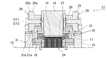
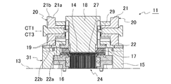
すなわち、上述した実施形態1では、ICパッケージ12を評価する際に、内側押圧部材16の押圧面16aでICパッケージ12を押圧するとともに、外側押圧部材19でソケット本体31の枠体15およびガイド部材17を押圧する場合について説明した。これに対して、実施形態2では、図16Aおよび図16Bに示すように、基部12c(本発明の「下段部」に対応)の上側に上部12d(本発明の「上段部」に対応)が形成された段付きのICパッケージ12をソケット本体31の収容部14に収容して評価する場合に、このICパッケージ12の上部12dを内側押圧部材16で押圧するとともに、このICパッケージ12の基部12cの周縁部を外側押圧部材19で押圧することにより、ICパッケージ12の反り上がりを抑えつつ、このICパッケージ12の評価を適正に実行することができる。
また、実施形態2では、基部12cの厚さT1または上部12dの厚さT2が異なるICパッケージ12を、それぞれ収容することができる。例えば、ICパッケージ12(本発明の「第3電気部品に対応」)の基部12cの厚さT1が同じであるとして、図16Aに示すように、ICパッケージ12の上部12dの厚さT2が厚い場合に、このICパッケージ12の基部12cおよび上部12dをそれぞれ外側押圧部材19および内側押圧部材16で適正に押圧できるように、カム20の第1押圧部21を基部12cの厚さT1および上部12dの厚さT2に対応させる。また、図16Bに示すように、ICパッケージ12(本発明の「第4電気部品に対応」)の上部12dの厚さT2がこれより薄い場合に、このICパッケージ12の基部12cおよび上部12dをそれぞれ外側押圧部材19および内側押圧部材16で適正に押圧できるように、カム20の第2押圧部22を基部12cの厚さT1および上部12dの厚さT2に対応させる。これにより、押圧箇所が2箇所(基部12cおよび上部12d)ある段付きのICパッケージ12の厚さの違いにも対応することが可能となる。
[発明のその他の実施の形態]
なお、上述した実施形態1、2では、第1押圧部21において、内側カム部21aと外側カム部21bとが互いに段差を生じているとともに、第2押圧部22において、内側カム部22aと外側カム部22bとが互いに段差を生じていないカム20について説明した。しかし、第1押圧部21および第2押圧部22の双方において、内側カム部21a、22aと外側カム部21b、22bとが互いに段差を生じるようにしても構わない。例えば、第1押圧部21では内側カム部21aと外側カム部21bとの段差(本発明の「第1段差」に対応)を大きくし、第2押圧部22では内側カム部22aと外側カム部22bとの段差(本発明の「第2段差」に対応)を小さくすることとすれば良い。
なお、上述した実施形態1、2では、第1押圧部21において、内側カム部21aと外側カム部21bとが互いに段差を生じているとともに、第2押圧部22において、内側カム部22aと外側カム部22bとが互いに段差を生じていないカム20について説明した。しかし、第1押圧部21および第2押圧部22の双方において、内側カム部21a、22aと外側カム部21b、22bとが互いに段差を生じるようにしても構わない。例えば、第1押圧部21では内側カム部21aと外側カム部21bとの段差(本発明の「第1段差」に対応)を大きくし、第2押圧部22では内側カム部22aと外側カム部22bとの段差(本発明の「第2段差」に対応)を小さくすることとすれば良い。
また、上述した実施形態1、2では、所定の各部の寸法関係(D3<D11<D12=D21=D22)を有するカム20について説明した。しかし、カム20の各部の寸法関係は、2種類のICパッケージ12の厚さの差や、内側押圧部材16および外側押圧部材19の位置関係などの状況に応じて適宜変更することができる。
また、上述した実施形態1、2では、略S字形のコンタクトピン26を有するICソケット11について説明した。しかし、コンタクトピン26の種類はこれに限らず、他の形状・構造(例えば、弓形のコンタクトピン、両端摺動型または片端摺動型のコンタクトピンなど)を代用することも可能である。
また、上述した実施形態1、2では、クラムシェルタイプのICソケット11について説明したが、クラムシェルタイプ以外のタイプ(例えば、いわゆるオープントップタイプなど)のICソケットにも、本発明を同様に適用することができる。
また、上述した実施形態1、2では、内側押圧部材16および外側押圧部材19を均等に押し下げられるように、略コ字形のベール25の両方の先端部に一対のカム20が取り付けられたICソケット11について説明した。しかし、内側押圧部材16および外側押圧部材19をカム20で均等に押し下げられる限り、カム20の個数は2個(一対)に限るわけではない。
また、上述した実施形態1、2では、内側押圧部材16にヒートシンク18が一体に設けられたICソケット11について説明した。しかし、ヒートシンク18は必ずしも内側押圧部材16と一体に設ける必要はなく、また、ICパッケージ12の発熱量が少ない場合にはヒートシンク18を省くことも可能である。
また、上述した実施形態2では、押圧箇所が2箇所ある仕様のICパッケージ12の一例として、段付きのICパッケージ12を取り上げて説明したが、段付きのICパッケージ12に限らず、押圧箇所が2箇所ある仕様のICパッケージに本発明を広く適用できることは言及するまでもない。
さらに、「電気部品用ソケット」としてのICソケット11に本発明を適用したが、これに限らず、他の装置にも適用できることは勿論である。
11……ICソケット(電気部品用ソケット)
12、12A、12B……ICパッケージ(電気部品)
14……収容部
16……内側押圧部材
18……ヒートシンク
19……外側押圧部材
20……カム
21……第1押圧部
21a……内側カム部
21b……外側カム部
22……第2押圧部
22a……内側カム部
22b……外側カム部
25……ベール
29……ソケットカバー
31……ソケット本体
12、12A、12B……ICパッケージ(電気部品)
14……収容部
16……内側押圧部材
18……ヒートシンク
19……外側押圧部材
20……カム
21……第1押圧部
21a……内側カム部
21b……外側カム部
22……第2押圧部
22a……内側カム部
22b……外側カム部
25……ベール
29……ソケットカバー
31……ソケット本体
Claims (8)
- 電気部品が着脱自在に収容される収容部を有するソケット本体と、
このソケット本体に前記収容部を開閉するように回動自在に設けられているソケットカバーと、
このソケットカバーに上下動自在に設けられて、前記ソケット本体の前記収容部に収容された前記電気部品を押圧する上下動自在な内側押圧部材と、
前記ソケットカバーに前記内側押圧部材より外側で当該内側押圧部材と独立して上下動自在に設けられて、前記ソケット本体の前記収容部に収容された前記電気部品または前記ソケット本体を押圧する外側押圧部材と、
前記ソケットカバーに回動自在に設けられて、一方向に回動させることにより、前記内側押圧部材および前記外側押圧部材を押し下げる第1押圧部が形成されているとともに、他方向に回動させることにより、前記内側押圧部材および前記外側押圧部材を押し下げる第2押圧部が形成されているカムと、
このカムを回転させるベールとを有する電気部品用ソケットであって、
前記カムには、前記第1押圧部に、前記内側押圧部材に接触して当該内側押圧部材を押し下げる第1内側カム部と、前記外側押圧部材に接触して当該外側押圧部材を押し下げる第1外側カム部とが、第1段差を生じるように形成されていることを特徴とする電気部品用ソケット。 - 前記カムの前記第2押圧部に、前記内側押圧部材に接触して当該内側押圧部材を押し下げる第2内側カム部と、前記外側押圧部材に接触して当該外側押圧部材を押し下げる第2外側カム部とが、段差を生じないように形成されていることを特徴とする請求項1に記載の電気部品用ソケット。
- 前記カムの前記第2押圧部に、前記内側押圧部材に接触して当該内側押圧部材を押し下げる第2内側カム部と、前記外側押圧部材に接触して当該外側押圧部材を押し下げる第2外側カム部とが、前記第1の段差よりも小さい第2段差を生じるように形成されていることを特徴とする請求項1に記載の電気部品用ソケット。
- 前記電気部品としての第1電気部品が前記ソケット本体の前記収容部に収容された場合に、前記カムが前記一方向に回動されて、前記第1押圧部が前記第1内側カム部で前記内側押圧部材を押し下げることにより前記第1電気部品を上方から押圧すると共に、前記第1外側カム部で前記外側押圧部材を押し下げることにより前記ソケット本体を上方から押圧し、
前記電気部品としての、前記第1電気部品よりも厚さが小さい第2電気部品が前記ソケット本体の前記収容部に収容された場合に、前記カムが前記他方向に回動されて、前記第2押圧部が前記第2内側カム部で前記内側押圧部材を押し下げることにより前記第2電気部品を上方から押圧すると共に、前記第2外側カム部で前記外側押圧部材を押し下げることにより前記ソケット本体を上方から押圧する、
ように構成されたことを特徴とする請求項2又は3に記載の電気部品用ソケット。 - 前記電気部品としての、段付の第3電気部品が前記ソケット本体の前記収容部に収容された場合に、前記カムが前記一方向に回動されて、前記第1押圧部が前記第1内側カム部で前記内側押圧部材を押し下げることにより前記第3電気部品の上段部を上方から押圧すると共に、前記第1外側カム部で前記外側押圧部材を押し下げることにより前記第3電気部品の下段部を上方から押圧し、
前記電気部品としての、前記第3電気部品よりも段差が小さい段付の第4電気部品が前記ソケット本体の前記収容部に収容された場合に、前記カムが前記他方向に回動されて、前記第2押圧部が前記第2内側カム部で前記内側押圧部材を押し下げることにより前記第4電気部品の上段部を上方から押圧すると共に、前記第2外側カム部で前記外側押圧部材を押し下げることにより前記第4電気部品の下段部上方から押圧する、
ように構成されたことを特徴とする請求項2又は3に記載の電気部品用ソケット。 - 前記ベールは略コ字形を呈しているとともに、このベールの両方の先端部に前記カムが1個ずつ計一対取り付けられており、前記ベールを操作することにより、前記一対のカムが回転可能に構成されていることを特徴とする請求項1に記載の電気部品用ソケット。
- 前記カムは、前記ベールに対して着脱自在に設けられていることを特徴とする請求項1に記載の電気部品用ソケット。
- 前記内側押圧部材にヒートシンクが設けられていることを特徴とする請求項1に記載の電気部品用ソケット。
Priority Applications (2)
| Application Number | Priority Date | Filing Date | Title |
|---|---|---|---|
| KR1020187036787A KR20190007057A (ko) | 2016-05-20 | 2017-05-16 | 전기부품용 소켓 |
| CN201780031232.5A CN109155496B (zh) | 2016-05-20 | 2017-05-16 | 电气部件用插座 |
Applications Claiming Priority (2)
| Application Number | Priority Date | Filing Date | Title |
|---|---|---|---|
| JP2016-101867 | 2016-05-20 | ||
| JP2016101867A JP6698426B2 (ja) | 2016-05-20 | 2016-05-20 | 電気部品用ソケット |
Publications (1)
| Publication Number | Publication Date |
|---|---|
| WO2017199937A1 true WO2017199937A1 (ja) | 2017-11-23 |
Family
ID=60326279
Family Applications (1)
| Application Number | Title | Priority Date | Filing Date |
|---|---|---|---|
| PCT/JP2017/018318 Ceased WO2017199937A1 (ja) | 2016-05-20 | 2017-05-16 | 電気部品用ソケット |
Country Status (5)
| Country | Link |
|---|---|
| JP (1) | JP6698426B2 (ja) |
| KR (1) | KR20190007057A (ja) |
| CN (1) | CN109155496B (ja) |
| TW (1) | TW201813222A (ja) |
| WO (1) | WO2017199937A1 (ja) |
Cited By (1)
| Publication number | Priority date | Publication date | Assignee | Title |
|---|---|---|---|---|
| KR20230087508A (ko) * | 2020-10-28 | 2023-06-16 | 야마이치 일렉트로닉스 컴퍼니 리미티드 | 히트 싱크 유닛, ic 소켓, 반도체 패키지의 제조방법 및 반도체 패키지 |
Families Citing this family (1)
| Publication number | Priority date | Publication date | Assignee | Title |
|---|---|---|---|---|
| JP2020143988A (ja) * | 2019-03-06 | 2020-09-10 | 株式会社エンプラス | ソケット |
Citations (3)
| Publication number | Priority date | Publication date | Assignee | Title |
|---|---|---|---|---|
| JP2002343518A (ja) * | 2001-05-17 | 2002-11-29 | Yamaichi Electronics Co Ltd | フラットパックicソケット |
| JP2013089297A (ja) * | 2011-10-13 | 2013-05-13 | Enplas Corp | 電気部用ソケット |
| WO2015152033A1 (ja) * | 2014-03-31 | 2015-10-08 | 株式会社エンプラス | 昇降機構及び電気部品用ソケット |
Family Cites Families (7)
| Publication number | Priority date | Publication date | Assignee | Title |
|---|---|---|---|---|
| JPH05290939A (ja) * | 1992-04-09 | 1993-11-05 | Mitsubishi Electric Corp | Icソケット |
| JP3619413B2 (ja) * | 2000-01-18 | 2005-02-09 | 株式会社エンプラス | 電気部品用ソケット |
| JP4487583B2 (ja) * | 2004-02-05 | 2010-06-23 | セイコーエプソン株式会社 | カム部材、及び当該カム部材を備えた記録装置 |
| JP4577200B2 (ja) * | 2005-12-08 | 2010-11-10 | 住友電装株式会社 | コネクタ装置 |
| JP4791328B2 (ja) * | 2006-10-27 | 2011-10-12 | 矢崎総業株式会社 | レバー式コネクタ |
| CN102201630A (zh) * | 2010-03-24 | 2011-09-28 | 世弘产业株式会社 | 可拆卸的插座装置 |
| JP6239382B2 (ja) | 2013-12-27 | 2017-11-29 | 株式会社エンプラス | 電気部品用ソケット |
-
2016
- 2016-05-20 JP JP2016101867A patent/JP6698426B2/ja not_active Expired - Fee Related
-
2017
- 2017-05-16 CN CN201780031232.5A patent/CN109155496B/zh not_active Expired - Fee Related
- 2017-05-16 KR KR1020187036787A patent/KR20190007057A/ko not_active Ceased
- 2017-05-16 WO PCT/JP2017/018318 patent/WO2017199937A1/ja not_active Ceased
- 2017-05-19 TW TW106116710A patent/TW201813222A/zh unknown
Patent Citations (3)
| Publication number | Priority date | Publication date | Assignee | Title |
|---|---|---|---|---|
| JP2002343518A (ja) * | 2001-05-17 | 2002-11-29 | Yamaichi Electronics Co Ltd | フラットパックicソケット |
| JP2013089297A (ja) * | 2011-10-13 | 2013-05-13 | Enplas Corp | 電気部用ソケット |
| WO2015152033A1 (ja) * | 2014-03-31 | 2015-10-08 | 株式会社エンプラス | 昇降機構及び電気部品用ソケット |
Cited By (3)
| Publication number | Priority date | Publication date | Assignee | Title |
|---|---|---|---|---|
| KR20230087508A (ko) * | 2020-10-28 | 2023-06-16 | 야마이치 일렉트로닉스 컴퍼니 리미티드 | 히트 싱크 유닛, ic 소켓, 반도체 패키지의 제조방법 및 반도체 패키지 |
| JP7538414B2 (ja) | 2020-10-28 | 2024-08-22 | 山一電機株式会社 | ヒートシンクユニット、icソケット、半導体パッケージの製造方法、及び半導体パッケージ |
| KR102798727B1 (ko) | 2020-10-28 | 2025-04-18 | 야마이치 일렉트로닉스 컴퍼니 리미티드 | 히트 싱크 유닛, ic 소켓, 반도체 패키지의 제조방법 및 반도체 패키지 |
Also Published As
| Publication number | Publication date |
|---|---|
| CN109155496A (zh) | 2019-01-04 |
| JP2017208305A (ja) | 2017-11-24 |
| KR20190007057A (ko) | 2019-01-21 |
| TW201813222A (zh) | 2018-04-01 |
| CN109155496B (zh) | 2020-06-02 |
| JP6698426B2 (ja) | 2020-05-27 |
Similar Documents
| Publication | Publication Date | Title |
|---|---|---|
| US9853380B2 (en) | Electronic component socket | |
| JP5383167B2 (ja) | 電気部品用ソケット | |
| US20140328037A1 (en) | Carrier and carrier assembly used thereof for positioning ic package | |
| JP4322635B2 (ja) | 電気部品用ソケット | |
| WO2017199937A1 (ja) | 電気部品用ソケット | |
| JP5584072B2 (ja) | 電気部品用ソケット | |
| JP2018029040A (ja) | 電気部品用ソケット | |
| JP6095982B2 (ja) | 電気部品用ソケット | |
| JP6400485B2 (ja) | 電気部品用ソケット | |
| KR101345816B1 (ko) | 반도체 패키지 테스트용 소켓 | |
| JP5095964B2 (ja) | ソケット用アタッチメント及びそれを有する半導体デバイス試験装置 | |
| JP5836113B2 (ja) | 電気部品用ソケット | |
| US10915181B2 (en) | Push button switch with operation unit latched to base | |
| US7247041B2 (en) | Land grid array connector | |
| US20060205259A1 (en) | IC package, IC socket, and IC socket assembly | |
| JP2003168534A (ja) | 電気部品用ソケット | |
| KR101345815B1 (ko) | 래치구조물 및 이를 포함하는 반도체 패키지 탑재용 소켓 | |
| JP4676841B2 (ja) | 電気部品用ソケット | |
| JP6400342B2 (ja) | 電気部品用ソケット | |
| JP2017219413A (ja) | 電気部品用ソケット | |
| JP2017027758A (ja) | 電気部品用ソケット | |
| CN112335140B (zh) | 电气部件用插座 | |
| JP5804495B2 (ja) | Icソケット | |
| JP2009158362A (ja) | 電気部品用ソケット | |
| JP2003223966A (ja) | 電気部品用ソケット及びこれに使用される移動板 |
Legal Events
| Date | Code | Title | Description |
|---|---|---|---|
| NENP | Non-entry into the national phase |
Ref country code: DE |
|
| 121 | Ep: the epo has been informed by wipo that ep was designated in this application |
Ref document number: 17799361 Country of ref document: EP Kind code of ref document: A1 |
|
| ENP | Entry into the national phase |
Ref document number: 20187036787 Country of ref document: KR Kind code of ref document: A |
|
| 122 | Ep: pct application non-entry in european phase |
Ref document number: 17799361 Country of ref document: EP Kind code of ref document: A1 |