WO2017188237A1 - Led光源装置 - Google Patents
Led光源装置 Download PDFInfo
- Publication number
- WO2017188237A1 WO2017188237A1 PCT/JP2017/016352 JP2017016352W WO2017188237A1 WO 2017188237 A1 WO2017188237 A1 WO 2017188237A1 JP 2017016352 W JP2017016352 W JP 2017016352W WO 2017188237 A1 WO2017188237 A1 WO 2017188237A1
- Authority
- WO
- WIPO (PCT)
- Prior art keywords
- main surface
- light source
- source device
- led light
- insulating substrate
- Prior art date
- Legal status (The legal status is an assumption and is not a legal conclusion. Google has not performed a legal analysis and makes no representation as to the accuracy of the status listed.)
- Ceased
Links
Images





Classifications
-
- H—ELECTRICITY
- H10—SEMICONDUCTOR DEVICES; ELECTRIC SOLID-STATE DEVICES NOT OTHERWISE PROVIDED FOR
- H10H—INORGANIC LIGHT-EMITTING SEMICONDUCTOR DEVICES HAVING POTENTIAL BARRIERS
- H10H20/00—Individual inorganic light-emitting semiconductor devices having potential barriers, e.g. light-emitting diodes [LED]
- H10H20/80—Constructional details
- H10H20/85—Packages
- H10H20/858—Means for heat extraction or cooling
Definitions
- the present invention relates to an LED light source device.
- the LED light source device includes a metal plate having a heat dissipation function, an insulating substrate disposed on the metal plate, having an opening exposing the metal plate, and having a wiring pattern formed on the upper surface, and a wiring pattern on the insulating substrate.
- a plurality of LED elements connected and mounted in two layers, each layer covered with a phosphor-containing resin, a circular sealing frame provided on an insulating substrate so as to surround the plurality of LED elements, and sealing And a sealing material made of a transparent resin with a diffusing material filled inside the frame.
- the LED light source device described in the conventional patent document 1 is mounted with the LED elements stacked, there is a possibility that the heat dissipation is inferior.
- the opening for exposing the metal plate is formed on the insulating substrate, when the LED elements are arranged without being stacked, there is a disadvantage that the number of LED elements that can be mounted is reduced by the opening.
- an object of the present invention is to provide an LED light source device that is excellent in heat dissipation and enables high-density mounting of LED elements.
- a wiring pattern is formed on the first main surface of the insulating base material, and a metal layer is formed on the second main surface opposite to the first main surface.
- a plurality of LED elements connected to the wiring pattern on the first main surface of the substrate and mounted at a predetermined mounting density, and a void ratio of the metal layer of the substrate equal to or lower than a predetermined value
- An LED light source device comprising: a heat dissipating member joined via a metal joining layer.
- heat dissipation is excellent, and high-density mounting of LED elements becomes possible.
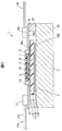
- FIG. 1 is a cross-sectional view schematically showing a schematic configuration of an LED light source device according to an embodiment of the present invention.
- FIG. 2 is a plan view of the LED light source device shown in FIG.
- FIG. 3 is a plan view of an LED light source device showing a modification of the frame member shown in FIG.
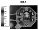
- FIG. 4A is a diagram illustrating temperature unevenness of Comparative Example 1 having a void ratio of 90%.
- FIG. 4B is a diagram illustrating a state of voids in Comparative Example 1 having a void ratio of 90%.
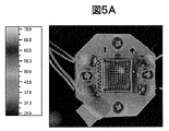
- FIG. 5A is a diagram showing temperature unevenness in Comparative Example 2 with a void ratio of 51%.
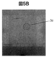
- FIG. 5B is a diagram showing a state of voids in Comparative Example 2 having a void ratio of 51%.
- FIG. 6A is a diagram illustrating temperature unevenness of Example 1 having a void ratio of 7%.
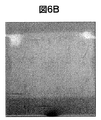
- FIG. 6B is a diagram illustrating a state of voids in Example 1 having a void ratio of 7%.
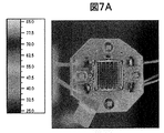
- FIG. 7A is a diagram showing temperature unevenness in Example 2 with a void ratio of 2%.
- FIG. 7B is a diagram illustrating a void state of Example 2 having a void ratio of 2%.
- FIG. 1 is a cross-sectional view schematically showing a schematic configuration of an LED light source device according to an embodiment of the present invention.
- FIG. 2 is a plan view of the LED light source device shown in FIG.
- the LED light source device 1 includes a metal block 2, an insulating substrate 4 provided on the upper surface 2 a of the metal block 2 via a solder layer 3, and a plurality of high-density mountings on the insulating substrate 4.
- a resin layer 7 and a sealing resin 8 that seals the surface of the phosphor-containing resin layer 7 are provided.
- the metal block 2 is an example of a heat dissipation member.
- the solder layer 3 is an example of a metal bonding layer.
- the phosphor-containing resin layer 7 and the sealing resin 8 are examples of a sealing material.
- the LED light source device 1 includes a power supply board 10 provided on the upper surface 2a of the metal block 2 via a spacer 9 and a pair of power supply harnesses 11A and 11B connected to the power supply board 10.
- the metal block 2 is made of metal such as copper, copper alloy, aluminum, aluminum alloy, for example.
- the metal block 2 has a surface area and volume equal to or larger than the surface area and volume of the insulating substrate 4.
- the metal block 2 is preferably formed with a through hole or a screw hole for fixing the metal block 2.
- it is preferable that the metal block 2 is surface-treated in order to prevent corrosion and form the solder layer 3.
- a heatsink having a large number of fins may be attached to the lower surface 2b of the metal block 2.
- the radiator is made of metal such as aluminum or aluminum alloy, for example. Further, the radiator may be provided with a heat pipe. The radiator may be provided with a forced cooling mechanism such as a fan or water cooling.
- the solder layer 3 has a void ratio indicating a void ratio of preferably 10% or less or 7% or less, and more preferably 2% or less.
- the solder layer 3 includes, for example, an Au—Sn alloy containing Au as a main component, an Sn—Cu alloy containing Sn as a main component, an Sn—Ag alloy, an Sn—Ag—Cu alloy, and an Sn—Ag— Bi based alloys, Sn—Zn based alloys and the like can be used.
- the thickness of the solder layer 3 depends on the size of the insulating substrate 4, for example, if it is about ⁇ 20 mm, it is preferably 0.2 mm or less or 0.1 mm or less, for example.
- the solder layer 3 having a low void ratio is formed by joining the metal block 2 and the insulating substrate 4 under reduced pressure (for example, 100 Pa to 20 kPa).
- the insulating substrate 4 is formed on the insulating base material 40, the wiring pattern 41 formed on the first main surface 40 a on the upper surface of the base material 40, and the second main surface 40 b on the lower surface of the base material 40. And a metal layer 42.
- the wiring pattern 41 is formed by etching a copper foil, for example.
- a copper foil can be used for the metal layer 42.
- One end of the wiring pattern 41 is connected to the electrode of the LED element 5, and the other end is connected to the connectors of the power supply harnesses 11 ⁇ / b> A and 11 ⁇ / b> B via the power supply substrate 10.
- a ceramic substrate such as aluminum nitride having a high thermal conductivity is preferably used from the viewpoint of heat dissipation and heat resistance.
- the LED element 5 may be a flip chip type having a pair of electrodes on the lower surface.
- the LED elements 5 are mounted on the insulating substrate 4 at a predetermined mounting density.
- the mounting density of the LED elements 5 is defined by the ratio of the total light emitting area to the mounting area.
- the mounting density is preferably 50% or more.
- the mounting area refers to the area inside the frame member 6.
- the light emission area is an area of the LED element 5 in plan view.
- the frame member 6 has, for example, a square shape and is formed of, for example, a silicone resin.
- the frame member 6 is not limited to a square, and may be other shapes such as a rectangle or a circle.
- the frame member 6 is preferably square or rectangular in order to increase the mounting density of the LED elements 5.
- the phosphor-containing resin layer 7 is formed by mixing a resin 70 and a granular phosphor 71 at a predetermined ratio.
- the resin 70 is formed of a material that is transparent to the emission wavelength of the LED element 5 and that can hold the phosphor 71.
- a resin material for example, a transparent resin such as an epoxy resin, a silicone resin, or an acrylic resin can be used.
- the color of the emitted light from the LED element 5 is blue and a phosphor that converts blue light into yellow light is used, part of the blue light emitted from the LED element 5 is converted into yellow light by the phosphor.
- the blue light and the yellow light that have been converted and emitted from the LED element 5 and not converted into yellow light by the phosphor are combined, and white light is emitted from the LED light source device 1.
- the sealing material 8 is formed from a material having transparency with respect to the emission wavelength of the LED element 5.
- a resin material for example, a transparent resin such as an epoxy resin, a silicone resin, or an acrylic resin can be used.
- the sealing material 8 may contain a diffusing material that diffuses the light emitted from the LED element 5.
- the power supply substrate 10 has an octagonal shape, but is not limited to this shape.
- the power supply substrate 10 has an opening 10a that is slightly larger than the outer shape of the frame member 6 so that the frame member 6 enters inside.
- a wiring pattern (not shown) is formed on the upper surface of the power supply substrate 10.
- One end of the wiring pattern of the power supply substrate 4 is electrically connected to the wiring pattern 41 of the insulating substrate 4 through the through hole 10b by solder, and the other end is electrically connected to the connector 111 of the power supply harnesses 11A and 11B. Is done.
- the power supply harnesses 11 ⁇ / b> A and 11 ⁇ / b> B include an electric wire 110 and a connector 111.
- the connector 111 is surface-mounted on the other end of the wiring pattern of the power supply substrate 10.
- the power supply harnesses 11 ⁇ / b> A and 11 ⁇ / b> B are electrically connected to the LED element 5 through the wiring pattern of the power supply substrate 10, the through hole 10 b and the wiring pattern 41 of the insulating substrate 4.
- FIG. 3 is a plan view of the LED light source device showing a modification of the frame member 6 shown in FIG.
- the frame member 16 may be circular.
- the power supply substrate 10 has an opening that is slightly larger than the outer shape of the frame member 16 so that the frame member 16 can enter inside.
- 4A, 4B, 5A, 5B, 6A, and 6B are diagrams showing the relationship between the void ratio of the solder layer 3 and temperature unevenness.
- 4A and 4B show Comparative Example 1 in which the void ratio is 90%, FIG. 4A shows temperature unevenness, and FIG. 4B shows the state of voids.
- 5A and 5B show Comparative Example 2 in which the void ratio is 51%, FIG. 5A shows temperature unevenness, and FIG. 5B shows the state of voids.
- 6A and 6B show Example 1 having a void ratio of 7%, FIG. 6A shows temperature unevenness, and FIG. 6B shows a void state.
- 7A and 7B show Example 2 in which the void ratio is 2%, FIG.
- FIG. 7A shows temperature unevenness
- FIG. 7B shows the state of voids
- 4A, 5A, 6A and 7A show the temperature scale on the left side
- 4B, FIG. 5B, FIG. 6B, and FIG. 7B are photographs taken by enlarging the area inside the frame member 6.
- Comparative Example 1, Comparative Example 2, Example 1 and Example 2 have a configuration corresponding to FIG. 2 except for the void ratio of the solder layer 3.
- the size of the power supply substrate 10 was 40 mm ⁇ 40 mm.
- Comparative Example 1 having a void ratio of 90%, since the voids 3a and 3b exist over a wide range as shown in FIG. 4B, a high temperature region of 70 ° C. or more is wide as shown in FIG. 4A. It can be seen that it exists over a range.
- Comparative Example 2 with a void ratio of 51%, as shown in FIG. 5B, since the void 3c exists, the range is narrower than that of Comparative Example 1 as shown in FIG. It can be seen that the area exists.
- Example 1 with a void ratio of 7% and Example 2 with a void ratio of 2% as shown in FIG. 6A and FIG. It can be seen that
- the third embodiment has a configuration corresponding to FIG.
- the size of the power supply substrate 10 was 60 mm ⁇ 60 mm.
- the LED element 5 having the same size in plan view as that of Example 1 and 1 mm ⁇ 1 mm was used.
- the mounting rate of the LED element 5 is 72% when the shape of the frame member 6 is square, whereas it is as small as 54% when the shape of the frame member 16 is circular. It can be seen that it is better to make the shape of the frame member square in order to increase the mounting rate.
- this invention is not limited to the said embodiment, In the range which does not change the summary of invention, it can deform
- the sealing material 8 may be omitted.
- the present invention can be applied to an LED light source device that has excellent heat dissipation and requires high-density mounting of LED elements.
- SYMBOLS 1 LED light source device, 2 ... Metal block, 2a ... Upper surface, 2b ... Lower surface, 3 ... Solder layer, 3a-3c ... Void, 4 ... Insulating substrate, 5 ... LED element, 6 ... Frame member, 7 ... Phosphor containing Resin layer, 8 ... sealing resin, 9 ... spacer, 10 ... power supply board, 10a ... opening, 10b ... through hole, 11A, 11B ... power supply harness, 16 ... frame member, 40 ... base material, 40a ... first Main surface, 40b ... second main surface, 41 ... wiring pattern, 42 ... metal layer, 70 ... resin, 71 ... phosphor, 110 ... electric wire, 111 ... connector
Landscapes
- Led Device Packages (AREA)
Abstract
放熱性に優れ、LED素子の高密度実装が可能なLED光源装置を提供するため、LED光源装置1は、絶縁性を有する基材40の第1の主面40aに配線パターン41が形成され、第1の主面40aと反対側の第2の主面40bに金属層42が形成された絶縁基板4と、絶縁基板4の第1の主面40aに配線パターン41に接続されて所定の実装密度で実装された複数のLED素子5と、絶縁基板4の金属層42にボイド率が所定の値以下のはんだ層3を介して接続された金属ブロック2とを備える。
Description
本発明は、LED光源装置に関する。
近年、発光ダイオード(LED)素子を高密度実装した高輝度高出力のLED光源装置が提案されている(特許文献1参照)。
このLED光源装置は、放熱機能を有する金属板と、金属板上に配置され、金属板を露出させる開口を有し、上面に配線パターンが形成された絶縁基板と、絶縁基板上に配線パターンに接続されて2層に実装され、層ごとに蛍光体含有樹脂で覆われた複数のLED素子と、複数のLED素子を囲むように絶縁基板上に設けられた円形の封止枠と、封止枠の内側に充填された拡散材入りの透明樹脂からなる封止材とを備える。
また、従来、LED素子に発生する熱を放熱し易くするため、LED素子をボイドのないAu-Sn合金はんだ層を介してアルミナ基板に接合したLED光源装置が提案されている(例えば、特許文献2参照。)。
しかし、従来の特許文献1に記載されたLED光源装置は、LED素子を重ねて実装しているため、放熱性に劣るおそれがある。また、絶縁基板に金属板を露出させるための開口を形成しているため、LED素子を重ねずに配置した場合には、開口によってLED素子を実装できる数が減るという欠点がある。
したがって、本発明の目的は、放熱性に優れ、LED素子の高密度実装が可能なLED光源装置を提供することにある。
本発明は、上記目的を達成するため、絶縁性を有する基材の第1の主面に配線パターンが形成され、前記第1の主面と反対側の第2の主面に金属層が形成された基板と、前記基板の前記第1の主面に前記配線パターンに接続されて所定の実装密度で実装された複数のLED素子と、前記基板の前記金属層にボイド率が所定の値以下の金属接合層を介して接合された放熱部材と、を備えたLED光源装置を提供する。
本発明によれば、放熱性に優れ、LED素子の高密度実装が可能になる。
以下、本発明の実施の形態及び実施例について図面を参照して説明する。なお、各図中、実質的に同一の機能を有する構成要素については、同一の符号を付してその重複した説明を省略する。
図1は、本発明の実施の形態に係るLED光源装置の概略の構成を模式的に示す断面図である。図2は、図1に示すLED光源装置の平面図である。
このLED光源装置1は、図1に示すように、金属ブロック2と、金属ブロック2の上面2aにはんだ層3を介して設けられた絶縁基板4と、絶縁基板4に高密度実装された複数のLED素子5と、複数のLED素子5全体を囲むように絶縁基板4上に形成された枠部材6と、枠部材6の内側に複数のLED素子5を覆うように形成された蛍光体含有樹脂層7と、蛍光体含有樹脂層7の表面を封止する封止樹脂8とを備える。ここで、金属ブロック2は、放熱部材の一例である。はんだ層3は、金属接合層の一例である。蛍光体含有樹脂層7及び封止樹脂8は、封止材の一例である。
また、LED光源装置1は、金属ブロック2の上面2aにスペーサ9を介して設けられた給電基板10と、給電基板10に接続された一対の給電用ハーネス11A、11Bとを備える。
金属ブロック2は、例えば、銅、銅合金、アルミニウム、アルミニウム合金等の金属から形成されている。金属ブロック2は、絶縁基板4の表面積及び体積と同等かそれよりも大きい表面積及び体積を有する。金属ブロック2は、金属ブロック2を固定するための貫通孔又はネジ穴が形成されているのが好ましい。また、金属ブロック2は、腐食防止、及びはんだ層3の形成のため、表面処理されているのが好ましい。
なお、放熱効果を高めるため、金属ブロック2の下面2bに、多数のフィンを有する放熱器を取り付けてもよい。放熱器は、例えば、アルミニウム又はアルミニウム合金等の金属から形成されている。また、放熱器は、ヒートパイプを備えたものでもよい。また、放熱器は、ファンや水冷等の強制冷却機構を備えたものでもよい。
はんだ層3は、放熱性の観点より、ボイドの割合を示すボイド率が10%以下又は7%以下が好ましく、2%以下がより好ましい。はんだ層3は、例えば、Auを主成分とするAu-Sn系合金や、Snを主成分とするSn-Cu系合金、Sn-Ag系合金、Sn-Ag-Cu系合金、Sn-Ag-Bi系合金、Sn-Zn系合金等を用いることができる。はんだ層3の厚さは、絶縁基板4のサイズにもよるが、例えば□20mm程度であれば、例えば0.2mm以下又は0.1mm以下が好ましい。ボイド率の低いはんだ層3は、金属ブロック2と絶縁基板4とを減圧(例えば、100Pa~20kPa)下で接合することにより形成される。
絶縁基板4は、絶縁性を有する基材40と、基材40の上面の第1の主面40aに形成された配線パターン41と、基材40の下面の第2の主面40bに形成された金属層42とを備える。配線パターン41は、例えば銅箔をエッチングして形成される。金属層42は、例えば銅箔を用いることができる。配線パターン41は、一端がLED素子5の電極に接続され、他端が給電基板10を介して給電用ハーネス11A、11Bのコネクタに接続される。基材40は、放熱性及び耐熱性の観点より、例えば、熱伝導率が大きい窒化アルミニウム等のセラミック基板を用いるのが好ましい。
LED素子5は、一対の電極を下面に有するフリップチップタイプのものを用いることができる。LED素子5は、例えば、青色光を出射する青色LED素子を用いることができる。LED素子5は、所定の実装密度で絶縁基板4上に実装されている。LED素子5の実装密度は、実装面積に対する発光面積の合計の比率で定義される。実装密度は、50%以上が好ましい。実装面積は、枠部材6の内側の面積をいう。発光面積は、LED素子5の平面視の面積である。
枠部材6は、例えば正方形を有し、例えばシリコーン樹脂から形成される。なお、枠部材6は、正方形に限られず、長方形でも円形等の他の形状でもよい。枠部材6は、正方形や長方形の方がLED素子5の実装密度を高める上で好ましい。
蛍光体含有樹脂層7は、樹脂70と粒状の蛍光体71とを所定の比率で混合して形成されたものである。樹脂70は、LED素子5の発光波長に対して透過性を有し、かつ、蛍光体71を保持できる材料から形成される。このような樹脂材料として、例えば、エポキシ樹脂、シリコーン樹脂、アクリル樹脂等の透明樹脂を用いることができる。
LED素子5の出射光の色を青色とし、蛍光体として青色の光を黄色の光に変換するものを用いた場合、LED素子5から出射された青色光の一部は蛍光体によって黄色光に変換され、LED素子5から出射され、蛍光体によって黄色光に変換されなかった青色光と黄色光とが合成されてLED光源装置1から白色光が出射される。
封止材8は、LED素子5の発光波長に対して透過性を有する材料から形成される。このような樹脂材料として、例えば、エポキシ樹脂、シリコーン樹脂、アクリル樹脂等の透明樹脂を用いることができる。なお、封止材8は、LED素子5から出射された光を拡散する拡散材を含有してもよい。
給電基板10は、図2に示すように、8角形を有するが、この形状に限定されない。給電基板10は、枠部材6が内側に入るように、枠部材6の外形よりもやや大きい開口10aを有する。給電基板10の上面に配線パターン(図示せず)が形成されている。給電基板4の配線パターンの一端は、スルーホール10bを介して絶縁基板4の配線パターン41にはんだにより電気的に接続され、他端は、給電用ハーネス11A、11Bのコネクタ111に電気的に接続される。
給電用ハーネス11A、11Bは、電線110と、コネクタ111とを備える。コネクタ111は、給電基板10の配線パターンの他端に表面実装されている。給電用ハーネス11A、11Bは、給電基板10の配線パターン、スルーホール10b及び絶縁基板4の配線パターン41を介してLED素子5に電気的に接続される。
(実施の形態の効果)
本実施の形態によれば、以下の作用、効果を奏する。
(a)LED素子5の基材として熱伝導率の高い窒化アルミニウム製の絶縁基板4を用い、この絶縁基板4に金属ブロック2を減圧下ではんだ接合しているので、LED素子5から金属ブロック2に至る熱抵抗が小さくなり、放熱性に優れたLED光源装置1を提供することができる。
(b)放熱性に優れた構造を有していることに加えて枠部材7を四角にしているため、枠部材7の内側にLED素子5を高密度実装することができる。
(c)絶縁基板4よりも表面積及び体積が大きい金属ブロック2を絶縁基板4に接合しているので、枠部材6の内側の実装面積(発熱面積)が小さくても十分に熱拡散ができ、放熱性に優れたLED光源装置1を提供することができる。
本実施の形態によれば、以下の作用、効果を奏する。
(a)LED素子5の基材として熱伝導率の高い窒化アルミニウム製の絶縁基板4を用い、この絶縁基板4に金属ブロック2を減圧下ではんだ接合しているので、LED素子5から金属ブロック2に至る熱抵抗が小さくなり、放熱性に優れたLED光源装置1を提供することができる。
(b)放熱性に優れた構造を有していることに加えて枠部材7を四角にしているため、枠部材7の内側にLED素子5を高密度実装することができる。
(c)絶縁基板4よりも表面積及び体積が大きい金属ブロック2を絶縁基板4に接合しているので、枠部材6の内側の実装面積(発熱面積)が小さくても十分に熱拡散ができ、放熱性に優れたLED光源装置1を提供することができる。
(枠部材の変形例)
図3は、図2に示す枠部材6の変形例を示すLED光源装置の平面図である。図3に示すように、枠部材16は円形でもよい。これにより、図2に示す枠部材6と比べてLED素子5の実装密度が小さくなるが、光束のゆがみが少なくなるという利点がある。給電基板10は、内側に枠部材16が入るように枠部材16の外形よりもやや大きい開口を有する。
図3は、図2に示す枠部材6の変形例を示すLED光源装置の平面図である。図3に示すように、枠部材16は円形でもよい。これにより、図2に示す枠部材6と比べてLED素子5の実装密度が小さくなるが、光束のゆがみが少なくなるという利点がある。給電基板10は、内側に枠部材16が入るように枠部材16の外形よりもやや大きい開口を有する。
(実施例1、2)
図4A、図4B、図5A、図5B、図6A及び図6Bは、はんだ層3のボイド率と温度ムラとの関係を示す図である。図4A及び図4Bは、ボイド率が90%の比較例1を示し、図4Aは温度ムラ、図4Bはボイドの状態を示す図である。図5A及び図5Bは、ボイド率が51%の比較例2を示し、図5Aは温度ムラ、図5Bはボイドの状態を示す図である。図6A及び図6Bは、ボイド率が7%の実施例1を示し、図6Aは温度ムラ、図6Bはボイドの状態を示す図である。図7A及び図7Bは、ボイド率が2%の実施例2を示し、図7Aは温度ムラ、図7Bはボイドの状態を示す図である。図4A、図5A、図6A、図7Aは、左側に温度のスケールを示す。図4B、図5B、図6B、図7Bは、いずれも枠部材6の内側の領域を拡大して撮影した写真である。
図4A、図4B、図5A、図5B、図6A及び図6Bは、はんだ層3のボイド率と温度ムラとの関係を示す図である。図4A及び図4Bは、ボイド率が90%の比較例1を示し、図4Aは温度ムラ、図4Bはボイドの状態を示す図である。図5A及び図5Bは、ボイド率が51%の比較例2を示し、図5Aは温度ムラ、図5Bはボイドの状態を示す図である。図6A及び図6Bは、ボイド率が7%の実施例1を示し、図6Aは温度ムラ、図6Bはボイドの状態を示す図である。図7A及び図7Bは、ボイド率が2%の実施例2を示し、図7Aは温度ムラ、図7Bはボイドの状態を示す図である。図4A、図5A、図6A、図7Aは、左側に温度のスケールを示す。図4B、図5B、図6B、図7Bは、いずれも枠部材6の内側の領域を拡大して撮影した写真である。
比較例1、比較例2、実施例1及び実施例2は、はんだ層3のボイド率を除いて図2に対応する構成を有する。給電基板10のサイズは、40mm×40mmとした。LED素子5は、平面視のサイズで1mm×1mmのものを用いたLED素子5の実装数は、11個×11個=121個とした。枠部材6の内側の面積(実装面積)は、13mm×13mm=169mm2とした。発光面積の合計は、121mm2とした。したがって、LED素子5の実装密度は、発光面積/実装面積=121/169=0.72=72%となる。
ボイド率が90%の比較例1は、図4Bに示すように、ボイド3a、3bが広い範囲に渡って存在しているため、図4Aに示すように、70℃以上の高温の領域が広い範囲に渡って存在していることが分かる。ボイド率が51%の比較例2は、図5Bに示すように、ボイド3cが存在しているため、図5Aに示すように、比較例1よりも範囲は狭いが、70℃以上の高温の領域が存在していることが分かる。ボイド率が7%の実施例1及びボイド率が2%の実施例2は、それぞれ図6A、図7Aに示すように、70℃以上の高温の領域は存在しておらず、優れた放熱効果を発揮していることが分かる。
(実施例3)
実施例3は、図3に対応する構成としたものである。給電基板10のサイズは、60mm×60mmとした。LED素子5は、実施例1と同じの平面視のサイズで1mm×1mmのものを用いた。LED素子5の実装数は、実施例1よりも増やして13個×13個=169個とした。枠部材16の内側の直径を20mmとしたことから、各部材16の内側の面積(実装面積)は、直径20mm×20mm×π/4=314mm2とした。発光面積の合計は、169mm2とした。したがって、LED素子5の実装密度は、発光面積/実装面積=169/314=0.54=54%となる。LED素子5の実装率は、枠部材6の形状が四角の場合、72%であるのに対し、枠部材16の形状が円形の場合、54%と小さくなった。実装率を高くするには、枠部材の形状を四角にした方がよいことが分かる。
実施例3は、図3に対応する構成としたものである。給電基板10のサイズは、60mm×60mmとした。LED素子5は、実施例1と同じの平面視のサイズで1mm×1mmのものを用いた。LED素子5の実装数は、実施例1よりも増やして13個×13個=169個とした。枠部材16の内側の直径を20mmとしたことから、各部材16の内側の面積(実装面積)は、直径20mm×20mm×π/4=314mm2とした。発光面積の合計は、169mm2とした。したがって、LED素子5の実装密度は、発光面積/実装面積=169/314=0.54=54%となる。LED素子5の実装率は、枠部材6の形状が四角の場合、72%であるのに対し、枠部材16の形状が円形の場合、54%と小さくなった。実装率を高くするには、枠部材の形状を四角にした方がよいことが分かる。
なお、本発明は、上記実施の形態に限定されず、発明の要旨を変更しない範囲内で種々に変形可能である。
また、本発明の要旨を変更しない範囲内で、上記実施の形態の構成要素の一部を省くことが可能である。例えば、封止材8を省いてもよい。
本発明は、放熱性に優れ、LED素子の高密度実装が必要なLED光源装置に適用することができる。
1…LED光源装置、2…金属ブロック、2a…上面、2b…下面、3…はんだ層、3a~3c…ボイド、4…絶縁基板、5…LED素子、6…枠部材、7…蛍光体含有樹脂層、8…封止樹脂、9…スペーサ、10…給電基板、10a…開口、10b…スルーホール、11A、11B…給電用ハーネス、16…枠部材、40…基材、40a…第1の主面、40b…第2の主面、41…配線パターン、42…金属層、70…樹脂、71…蛍光体、110…電線、111…コネクタ
Claims (5)
- 絶縁性を有する基材の第1の主面に配線パターンが形成され、前記第1の主面と反対側の第2の主面に金属層が形成された基板と、
前記基板の前記第1の主面に前記配線パターンに接続されて所定の実装密度で実装された複数のLED素子と、
前記基板の前記金属層にボイド率が所定の値以下の金属接合層を介して接合された放熱部材と、
を備えたLED光源装置。 - 前記金属接合層の前記ボイド率は、7%以下である、
請求項1に記載のLED光源装置。 - 前記LED素子の実装密度は、実装面積に対する発光面積の合計が50%以上である、
請求項1又は2に記載のLED光源装置。 - 前記基板は、窒化アルミニウムからなる、請求項1から3のいずれか1項に記載のLED光源装置。
- 絶縁性を有する基材の第1の主面に配線パターンが形成され、前記第1の主面と反対側の第2の主面に金属層が形成された窒化アルミニウムからなる絶縁基板と、
前記絶縁基板の前記第1の主面に前記配線パターンに接続されて50%以上の実装密度でフリップチップ実装された複数のLED素子と、
前記絶縁基板上に前記複数のLED素子を囲むように設けられた枠部材と、
前記枠部材の内側に封止された透光性を有する封止部材と、
前記絶縁基板の表面積及び体積よりも大きい表面積及び体積を有し、前記絶縁基板の前記金属層にボイド率が7%以下のはんだ層を介して接合された放熱部材と、
を備えたLED光源装置。
Applications Claiming Priority (2)
| Application Number | Priority Date | Filing Date | Title |
|---|---|---|---|
| JP2016090643A JP2017199842A (ja) | 2016-04-28 | 2016-04-28 | Led光源装置 |
| JP2016-090643 | 2016-04-28 |
Publications (1)
| Publication Number | Publication Date |
|---|---|
| WO2017188237A1 true WO2017188237A1 (ja) | 2017-11-02 |
Family
ID=60161537
Family Applications (1)
| Application Number | Title | Priority Date | Filing Date |
|---|---|---|---|
| PCT/JP2017/016352 Ceased WO2017188237A1 (ja) | 2016-04-28 | 2017-04-25 | Led光源装置 |
Country Status (2)
| Country | Link |
|---|---|
| JP (1) | JP2017199842A (ja) |
| WO (1) | WO2017188237A1 (ja) |
Cited By (4)
| Publication number | Priority date | Publication date | Assignee | Title |
|---|---|---|---|---|
| WO2020184371A1 (ja) | 2019-03-08 | 2020-09-17 | 京セラ株式会社 | 接合体および光源装置 |
| WO2021039825A1 (ja) | 2019-08-28 | 2021-03-04 | 京セラ株式会社 | 発光素子搭載用パッケージおよび発光装置 |
| WO2021060475A1 (ja) | 2019-09-25 | 2021-04-01 | 京セラ株式会社 | 電子部品搭載用基体および電子装置 |
| WO2021193607A1 (ja) | 2020-03-27 | 2021-09-30 | 京セラ株式会社 | 電子部品搭載用基板および電子装置 |
Citations (5)
| Publication number | Priority date | Publication date | Assignee | Title |
|---|---|---|---|---|
| JP2005205418A (ja) * | 2004-01-20 | 2005-08-04 | Denso Corp | 接合構造体の製造方法 |
| JP2008010545A (ja) * | 2006-06-28 | 2008-01-17 | Mitsubishi Materials Corp | Au−Sn合金はんだペーストを用いて素子の接合面全面を基板に接合する方法 |
| US20090243089A1 (en) * | 2008-03-31 | 2009-10-01 | Infineon Technologies Ag | Module including a rough solder joint |
| JP2014132629A (ja) * | 2012-12-07 | 2014-07-17 | Toshiba Lighting & Technology Corp | 発光装置及び照明装置 |
| CN104501013A (zh) * | 2014-12-24 | 2015-04-08 | 付斌 | Led灯具 |
Family Cites Families (10)
| Publication number | Priority date | Publication date | Assignee | Title |
|---|---|---|---|---|
| JP2510557B2 (ja) * | 1986-10-17 | 1996-06-26 | 株式会社日立製作所 | 複合構造体の製造方法 |
| JPH04141606A (ja) * | 1990-10-02 | 1992-05-15 | Hitachi Ltd | 光電子装置 |
| JP4404000B2 (ja) * | 2005-04-05 | 2010-01-27 | トヨタ自動車株式会社 | 接合構造体の製造方法 |
| JP2010114197A (ja) * | 2008-11-05 | 2010-05-20 | Toshiba Corp | 半導体部品の製造方法 |
| CN101994929A (zh) * | 2009-08-20 | 2011-03-30 | 启耀光电股份有限公司 | 发光模块 |
| JP2013004752A (ja) * | 2011-06-16 | 2013-01-07 | Fujikura Ltd | レーザモジュール |
| JP2013201255A (ja) * | 2012-03-23 | 2013-10-03 | Toshiba Lighting & Technology Corp | 配線基板装置、発光モジュール、照明装置および配線基板装置の製造方法 |
| JP2014110397A (ja) * | 2012-12-04 | 2014-06-12 | Toshiba Lighting & Technology Corp | 発光装置 |
| JP2015186810A (ja) * | 2014-03-26 | 2015-10-29 | 株式会社フジクラ | はんだ接合方法、ldモジュールの製造方法、および、はんだ接合装置 |
| KR101860378B1 (ko) * | 2014-04-04 | 2018-05-23 | 쿄세라 코포레이션 | 열경화성 수지 조성물, 반도체 장치 및 전기·전자 부품 |
-
2016
- 2016-04-28 JP JP2016090643A patent/JP2017199842A/ja active Pending
-
2017
- 2017-04-25 WO PCT/JP2017/016352 patent/WO2017188237A1/ja not_active Ceased
Patent Citations (5)
| Publication number | Priority date | Publication date | Assignee | Title |
|---|---|---|---|---|
| JP2005205418A (ja) * | 2004-01-20 | 2005-08-04 | Denso Corp | 接合構造体の製造方法 |
| JP2008010545A (ja) * | 2006-06-28 | 2008-01-17 | Mitsubishi Materials Corp | Au−Sn合金はんだペーストを用いて素子の接合面全面を基板に接合する方法 |
| US20090243089A1 (en) * | 2008-03-31 | 2009-10-01 | Infineon Technologies Ag | Module including a rough solder joint |
| JP2014132629A (ja) * | 2012-12-07 | 2014-07-17 | Toshiba Lighting & Technology Corp | 発光装置及び照明装置 |
| CN104501013A (zh) * | 2014-12-24 | 2015-04-08 | 付斌 | Led灯具 |
Cited By (11)
| Publication number | Priority date | Publication date | Assignee | Title |
|---|---|---|---|---|
| WO2020184371A1 (ja) | 2019-03-08 | 2020-09-17 | 京セラ株式会社 | 接合体および光源装置 |
| CN113490592A (zh) * | 2019-03-08 | 2021-10-08 | 京瓷株式会社 | 接合体和光源装置 |
| JPWO2020184371A1 (ja) * | 2019-03-08 | 2021-12-23 | 京セラ株式会社 | 接合体および光源装置 |
| JP7187664B2 (ja) | 2019-03-08 | 2022-12-12 | 京セラ株式会社 | 接合体および光源装置 |
| CN113490592B (zh) * | 2019-03-08 | 2023-10-24 | 京瓷株式会社 | 接合体和光源装置 |
| US12206057B2 (en) | 2019-03-08 | 2025-01-21 | Kyocera Corporation | Joint body and light source device |
| WO2021039825A1 (ja) | 2019-08-28 | 2021-03-04 | 京セラ株式会社 | 発光素子搭載用パッケージおよび発光装置 |
| WO2021060475A1 (ja) | 2019-09-25 | 2021-04-01 | 京セラ株式会社 | 電子部品搭載用基体および電子装置 |
| US12362254B2 (en) | 2019-09-25 | 2025-07-15 | Kyocera Corporation | Electronic component mounting base and electronic device |
| WO2021193607A1 (ja) | 2020-03-27 | 2021-09-30 | 京セラ株式会社 | 電子部品搭載用基板および電子装置 |
| US12224390B2 (en) | 2020-03-27 | 2025-02-11 | Kyocera Corporation | Electronic component mounting substrate and electronic device |
Also Published As
| Publication number | Publication date |
|---|---|
| JP2017199842A (ja) | 2017-11-02 |
Similar Documents
| Publication | Publication Date | Title |
|---|---|---|
| JP4123105B2 (ja) | 発光装置 | |
| CN102263095B (zh) | 发光装置以及照明装置 | |
| JP5421751B2 (ja) | 半導体発光装置 | |
| JP5082083B2 (ja) | Led照明装置 | |
| JP2006049442A (ja) | 半導体発光装置およびその製造方法 | |
| JP5288642B2 (ja) | 発光素子 | |
| US20180062059A1 (en) | Light-emitting module, lighting apparatus for mobile object, and mobile object | |
| JP5124688B2 (ja) | 照明装置、ディスプレイ、及び信号灯 | |
| JP2009054801A (ja) | 放熱部材及びそれを備えた発光モジュール | |
| WO2018105448A1 (ja) | 発光装置 | |
| WO2017188237A1 (ja) | Led光源装置 | |
| US10236429B2 (en) | Mounting assembly and lighting device | |
| CN109994458A (zh) | 发光装置 | |
| JP4938611B2 (ja) | 半導体発光装置 | |
| JP2009021384A (ja) | 電子部品及び発光装置 | |
| JP2015087508A (ja) | 投写型表示装置 | |
| JP4821343B2 (ja) | サブマウント基板及びこれを備える発光装置 | |
| JP2010080796A (ja) | 照明装置 | |
| JP2009038156A (ja) | 回路基板及び照明装置 | |
| JP6210720B2 (ja) | Ledパッケージ | |
| KR101135580B1 (ko) | 발광 다이오드 조명 모듈 | |
| JP2013030598A (ja) | 発熱デバイス | |
| JP6085459B2 (ja) | 照明装置 | |
| JP5538989B2 (ja) | 発光ダイオード構造 | |
| JP2009021383A (ja) | 電子部品 |
Legal Events
| Date | Code | Title | Description |
|---|---|---|---|
| NENP | Non-entry into the national phase |
Ref country code: DE |
|
| 121 | Ep: the epo has been informed by wipo that ep was designated in this application |
Ref document number: 17789519 Country of ref document: EP Kind code of ref document: A1 |
|
| 122 | Ep: pct application non-entry in european phase |
Ref document number: 17789519 Country of ref document: EP Kind code of ref document: A1 |