WO2017183222A1 - 半導体装置およびその製造方法 - Google Patents
半導体装置およびその製造方法 Download PDFInfo
- Publication number
- WO2017183222A1 WO2017183222A1 PCT/JP2016/082199 JP2016082199W WO2017183222A1 WO 2017183222 A1 WO2017183222 A1 WO 2017183222A1 JP 2016082199 W JP2016082199 W JP 2016082199W WO 2017183222 A1 WO2017183222 A1 WO 2017183222A1
- Authority
- WO
- WIPO (PCT)
- Prior art keywords
- semiconductor element
- semiconductor device
- conductive plate
- semiconductor
- insulating substrate
- Prior art date
Links
Images


Classifications
-
- H—ELECTRICITY
- H01—ELECTRIC ELEMENTS
- H01L—SEMICONDUCTOR DEVICES NOT COVERED BY CLASS H10
- H01L23/00—Details of semiconductor or other solid state devices
- H01L23/34—Arrangements for cooling, heating, ventilating or temperature compensation ; Temperature sensing arrangements
- H01L23/40—Mountings or securing means for detachable cooling or heating arrangements ; fixed by friction, plugs or springs
-
- H—ELECTRICITY
- H01—ELECTRIC ELEMENTS
- H01L—SEMICONDUCTOR DEVICES NOT COVERED BY CLASS H10
- H01L21/00—Processes or apparatus adapted for the manufacture or treatment of semiconductor or solid state devices or of parts thereof
- H01L21/02—Manufacture or treatment of semiconductor devices or of parts thereof
- H01L21/04—Manufacture or treatment of semiconductor devices or of parts thereof the devices having at least one potential-jump barrier or surface barrier, e.g. PN junction, depletion layer or carrier concentration layer
- H01L21/50—Assembly of semiconductor devices using processes or apparatus not provided for in a single one of the subgroups H01L21/06 - H01L21/326, e.g. sealing of a cap to a base of a container
- H01L21/52—Mounting semiconductor bodies in containers
-
- H—ELECTRICITY
- H01—ELECTRIC ELEMENTS
- H01L—SEMICONDUCTOR DEVICES NOT COVERED BY CLASS H10
- H01L21/00—Processes or apparatus adapted for the manufacture or treatment of semiconductor or solid state devices or of parts thereof
- H01L21/02—Manufacture or treatment of semiconductor devices or of parts thereof
- H01L21/04—Manufacture or treatment of semiconductor devices or of parts thereof the devices having at least one potential-jump barrier or surface barrier, e.g. PN junction, depletion layer or carrier concentration layer
- H01L21/50—Assembly of semiconductor devices using processes or apparatus not provided for in a single one of the subgroups H01L21/06 - H01L21/326, e.g. sealing of a cap to a base of a container
- H01L21/56—Encapsulations, e.g. encapsulation layers, coatings
-
- H—ELECTRICITY
- H01—ELECTRIC ELEMENTS
- H01L—SEMICONDUCTOR DEVICES NOT COVERED BY CLASS H10
- H01L23/00—Details of semiconductor or other solid state devices
- H01L23/34—Arrangements for cooling, heating, ventilating or temperature compensation ; Temperature sensing arrangements
- H01L23/36—Selection of materials, or shaping, to facilitate cooling or heating, e.g. heatsinks
- H01L23/373—Cooling facilitated by selection of materials for the device or materials for thermal expansion adaptation, e.g. carbon
- H01L23/3735—Laminates or multilayers, e.g. direct bond copper ceramic substrates
-
- H—ELECTRICITY
- H01—ELECTRIC ELEMENTS
- H01L—SEMICONDUCTOR DEVICES NOT COVERED BY CLASS H10
- H01L23/00—Details of semiconductor or other solid state devices
- H01L23/34—Arrangements for cooling, heating, ventilating or temperature compensation ; Temperature sensing arrangements
- H01L23/36—Selection of materials, or shaping, to facilitate cooling or heating, e.g. heatsinks
- H01L23/373—Cooling facilitated by selection of materials for the device or materials for thermal expansion adaptation, e.g. carbon
- H01L23/3736—Metallic materials
-
- H—ELECTRICITY
- H01—ELECTRIC ELEMENTS
- H01L—SEMICONDUCTOR DEVICES NOT COVERED BY CLASS H10
- H01L25/00—Assemblies consisting of a plurality of individual semiconductor or other solid state devices ; Multistep manufacturing processes thereof
- H01L25/03—Assemblies consisting of a plurality of individual semiconductor or other solid state devices ; Multistep manufacturing processes thereof all the devices being of a type provided for in the same subgroup of groups H01L27/00 - H01L33/00, or in a single subclass of H10K, H10N, e.g. assemblies of rectifier diodes
- H01L25/04—Assemblies consisting of a plurality of individual semiconductor or other solid state devices ; Multistep manufacturing processes thereof all the devices being of a type provided for in the same subgroup of groups H01L27/00 - H01L33/00, or in a single subclass of H10K, H10N, e.g. assemblies of rectifier diodes the devices not having separate containers
- H01L25/07—Assemblies consisting of a plurality of individual semiconductor or other solid state devices ; Multistep manufacturing processes thereof all the devices being of a type provided for in the same subgroup of groups H01L27/00 - H01L33/00, or in a single subclass of H10K, H10N, e.g. assemblies of rectifier diodes the devices not having separate containers the devices being of a type provided for in group H01L29/00
-
- H—ELECTRICITY
- H01—ELECTRIC ELEMENTS
- H01L—SEMICONDUCTOR DEVICES NOT COVERED BY CLASS H10
- H01L25/00—Assemblies consisting of a plurality of individual semiconductor or other solid state devices ; Multistep manufacturing processes thereof
- H01L25/18—Assemblies consisting of a plurality of individual semiconductor or other solid state devices ; Multistep manufacturing processes thereof the devices being of types provided for in two or more different subgroups of the same main group of groups H01L27/00 - H01L33/00, or in a single subclass of H10K, H10N
-
- H—ELECTRICITY
- H01—ELECTRIC ELEMENTS
- H01L—SEMICONDUCTOR DEVICES NOT COVERED BY CLASS H10
- H01L2224/00—Indexing scheme for arrangements for connecting or disconnecting semiconductor or solid-state bodies and methods related thereto as covered by H01L24/00
- H01L2224/01—Means for bonding being attached to, or being formed on, the surface to be connected, e.g. chip-to-package, die-attach, "first-level" interconnects; Manufacturing methods related thereto
- H01L2224/26—Layer connectors, e.g. plate connectors, solder or adhesive layers; Manufacturing methods related thereto
- H01L2224/31—Structure, shape, material or disposition of the layer connectors after the connecting process
- H01L2224/32—Structure, shape, material or disposition of the layer connectors after the connecting process of an individual layer connector
- H01L2224/321—Disposition
- H01L2224/32151—Disposition the layer connector connecting between a semiconductor or solid-state body and an item not being a semiconductor or solid-state body, e.g. chip-to-substrate, chip-to-passive
- H01L2224/32221—Disposition the layer connector connecting between a semiconductor or solid-state body and an item not being a semiconductor or solid-state body, e.g. chip-to-substrate, chip-to-passive the body and the item being stacked
- H01L2224/32225—Disposition the layer connector connecting between a semiconductor or solid-state body and an item not being a semiconductor or solid-state body, e.g. chip-to-substrate, chip-to-passive the body and the item being stacked the item being non-metallic, e.g. insulating substrate with or without metallisation
-
- H—ELECTRICITY
- H01—ELECTRIC ELEMENTS
- H01L—SEMICONDUCTOR DEVICES NOT COVERED BY CLASS H10
- H01L2224/00—Indexing scheme for arrangements for connecting or disconnecting semiconductor or solid-state bodies and methods related thereto as covered by H01L24/00
- H01L2224/01—Means for bonding being attached to, or being formed on, the surface to be connected, e.g. chip-to-package, die-attach, "first-level" interconnects; Manufacturing methods related thereto
- H01L2224/42—Wire connectors; Manufacturing methods related thereto
- H01L2224/47—Structure, shape, material or disposition of the wire connectors after the connecting process
- H01L2224/48—Structure, shape, material or disposition of the wire connectors after the connecting process of an individual wire connector
- H01L2224/4805—Shape
- H01L2224/4809—Loop shape
- H01L2224/48091—Arched
-
- H—ELECTRICITY
- H01—ELECTRIC ELEMENTS
- H01L—SEMICONDUCTOR DEVICES NOT COVERED BY CLASS H10
- H01L2224/00—Indexing scheme for arrangements for connecting or disconnecting semiconductor or solid-state bodies and methods related thereto as covered by H01L24/00
- H01L2224/73—Means for bonding being of different types provided for in two or more of groups H01L2224/10, H01L2224/18, H01L2224/26, H01L2224/34, H01L2224/42, H01L2224/50, H01L2224/63, H01L2224/71
- H01L2224/732—Location after the connecting process
- H01L2224/73251—Location after the connecting process on different surfaces
- H01L2224/73265—Layer and wire connectors
-
- H—ELECTRICITY
- H01—ELECTRIC ELEMENTS
- H01L—SEMICONDUCTOR DEVICES NOT COVERED BY CLASS H10
- H01L2924/00—Indexing scheme for arrangements or methods for connecting or disconnecting semiconductor or solid-state bodies as covered by H01L24/00
-
- H—ELECTRICITY
- H01—ELECTRIC ELEMENTS
- H01L—SEMICONDUCTOR DEVICES NOT COVERED BY CLASS H10
- H01L2924/00—Indexing scheme for arrangements or methods for connecting or disconnecting semiconductor or solid-state bodies as covered by H01L24/00
- H01L2924/0001—Technical content checked by a classifier
- H01L2924/00012—Relevant to the scope of the group, the symbol of which is combined with the symbol of this group
-
- H—ELECTRICITY
- H01—ELECTRIC ELEMENTS
- H01L—SEMICONDUCTOR DEVICES NOT COVERED BY CLASS H10
- H01L2924/00—Indexing scheme for arrangements or methods for connecting or disconnecting semiconductor or solid-state bodies as covered by H01L24/00
- H01L2924/0001—Technical content checked by a classifier
- H01L2924/00014—Technical content checked by a classifier the subject-matter covered by the group, the symbol of which is combined with the symbol of this group, being disclosed without further technical details
-
- H—ELECTRICITY
- H01—ELECTRIC ELEMENTS
- H01L—SEMICONDUCTOR DEVICES NOT COVERED BY CLASS H10
- H01L2924/00—Indexing scheme for arrangements or methods for connecting or disconnecting semiconductor or solid-state bodies as covered by H01L24/00
- H01L2924/10—Details of semiconductor or other solid state devices to be connected
- H01L2924/11—Device type
- H01L2924/13—Discrete devices, e.g. 3 terminal devices
- H01L2924/1304—Transistor
- H01L2924/1305—Bipolar Junction Transistor [BJT]
- H01L2924/13055—Insulated gate bipolar transistor [IGBT]
-
- H—ELECTRICITY
- H01—ELECTRIC ELEMENTS
- H01L—SEMICONDUCTOR DEVICES NOT COVERED BY CLASS H10
- H01L2924/00—Indexing scheme for arrangements or methods for connecting or disconnecting semiconductor or solid-state bodies as covered by H01L24/00
- H01L2924/19—Details of hybrid assemblies other than the semiconductor or other solid state devices to be connected
- H01L2924/191—Disposition
- H01L2924/19101—Disposition of discrete passive components
- H01L2924/19107—Disposition of discrete passive components off-chip wires
Definitions
- the present invention relates to a semiconductor device and a manufacturing method thereof.
- semiconductor elements based on Si (silicon) or SiC (silicon carbide) are used. Since it is necessary to keep the temperature of the semiconductor element below a predetermined temperature, it is desirable to efficiently dissipate the heat generated from the semiconductor element.
- an insulating ceramic plate having a high thermal conductivity and a conductive plate made of a metal having a high thermal conductivity provided on both surfaces thereof are integrated.
- silicon nitride, aluminum nitride, or alumina is used for the insulating ceramic plate.
- aluminum (including an aluminum alloy; hereinafter the same) or copper (including a copper alloy; hereinafter the same) is used for the conductive plate.
- the semiconductor element is bonded to one surface of the insulating substrate via a sintered metal such as sintered Ag.
- a cooler is joined directly or indirectly to the other surface of the insulating substrate via a joining material such as solder.
- a semiconductor element has also been proposed from the viewpoint of suppressing deformation of the resin that seals the semiconductor device. Such deformation is caused, for example, by a temperature change in the external environment.
- a semiconductor element having a bending strength of 100 MPa or more and 1000 MPa or less is arranged as a stress relaxation member.
- the stress relaxation member in Patent Document 1 is made of a semiconductor element having a bending strength of 100 MPa or more and 1000 MPa or less arranged on the main surface of the insulating substrate.
- a semiconductor device including a stress relaxation member disclosed in Patent Document 1 has a problem in a direct cooling type module in which a cooler and an insulating substrate are directly joined with solder. On the insulating substrate, there is an Ag sintering portion joined to a semiconductor element (for example, a SiC chip).
- a semiconductor element for example, a SiC chip.
- SiC is expected to withstand a higher junction temperature than Si, and a heat cycle in which high temperature / low temperature is repeated is 175 ° C. or higher at the high temperature. When operating in such a heat cycle, cracks may occur in the Ag sinter part.
- the present invention has been made to solve the above problems, and an object thereof is to provide a semiconductor device having high thermal conductivity and excellent workability, and a method for manufacturing the same.
- the semiconductor device includes an insulating plate, an insulating plate having a first conductive plate provided on one surface of the insulating plate, and a second conductive plate provided on the other surface of the insulating plate.
- a substrate is provided.
- the bending strength of the semiconductor element is 700 MPa or more.
- the semiconductor element has a crack growth depth rate of 30% or less of its chip thickness.
- the method of manufacturing a semiconductor device includes: (a) an insulating plate; a first conductive plate provided on one surface of the insulating plate; and a second conductive plate provided on the other surface of the insulating plate.
- a step of providing an insulating substrate having a conductive plate (b) a step of providing a semiconductor element on the first conductive plate via a sintered metal, and (c) a first of the second conductive plate. And a step of bonding the cooling member via the bonding material.
- the thermal stress due to the difference between the linear expansion coefficient of the semiconductor element and the thermal expansion coefficient of the cooling member is absorbed by the semiconductor element. Therefore, while increasing the thermal conductivity, the stress generated in the bonding material is relieved and the workability is excellent.
- the method for manufacturing a semiconductor device according to the present invention contributes to the manufacture of the semiconductor device according to the present invention.
- FIG. 1 is a cross-sectional view showing a structure of a semiconductor device according to a first embodiment; It is sectional drawing which shows the manufacturing process of a semiconductor element in order. It is sectional drawing which shows the manufacturing process of a semiconductor element in order. It is sectional drawing which shows the manufacturing process of a semiconductor element in order. It is sectional drawing which shows the manufacturing process of a semiconductor element in order. It is sectional drawing which shows the process before manufacturing a semiconductor device after manufacturing a semiconductor element. It is a graph which shows the relationship of the lifetime of the die-bonding material with respect to the linear expansion coefficient of an insulated substrate. It is a SAT image which shows the peeling which generate
- FIG. 6 is a cross-sectional view showing a structure of a semiconductor device according to a second embodiment; FIG. FIG. 6 is a cross-sectional view sequentially showing a manufacturing process of a semiconductor device according to a second embodiment; FIG.
- FIG. 6 is a cross-sectional view sequentially showing a manufacturing process of a semiconductor device according to a second embodiment; 6 is a cross-sectional view showing a structure of a semiconductor device according to a second embodiment; FIG. FIG. 6 is a cross-sectional view showing the structure of another semiconductor device according to the second embodiment.
- FIG. 6 is a sectional view showing a structure of a semiconductor device according to a fourth embodiment.
- FIG. 9 is a cross-sectional view sequentially showing manufacturing steps of a semiconductor device according to a fourth embodiment.
- FIG. 9 is a cross-sectional view sequentially showing manufacturing steps of a semiconductor device according to a fourth embodiment.
- FIG. 9 is a cross-sectional view sequentially showing manufacturing steps of a semiconductor device according to a fourth embodiment.
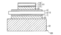
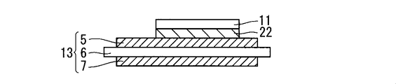
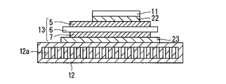
- FIG. 1 is a sectional view showing the structure of the semiconductor device 101 according to the first embodiment.
- the semiconductor device 101 includes a semiconductor element 11, a die bond material 22, an insulating substrate 13, a bonding material 23, and a cooling member 12.
- the semiconductor element 11 is bonded to one surface of the insulating substrate 13 via a die bond material 22.
- the other surface of the insulating substrate 13 and the cooling member 12 are bonded via a bonding material 23.
- the insulating substrate 13 includes an insulating ceramic 6 as an insulating plate, a conductive plate 5 provided on one surface of the insulating ceramic 6, and a conductive plate 7 provided on the other surface.
- the insulating substrate 13 includes the conductive plates 5 and 7 and the insulating ceramics 6 disposed between the conductive plate 5 and the conductive plate 7. These are integrated in advance as an insulating substrate 13 using a brazing material or the like.
- the conductive plate 5 is in contact with the die bond material 22. Therefore, the semiconductor element 11 is provided on the conductive plate 5 via the die bonding material 22, and more specifically, bonded to the conductive plate 5.
- the die bonding material 22 may be omitted by bonding the semiconductor element 11 and the insulating substrate 13 by direct bonding such as Cu solid phase diffusion bonding or ultrasonic bonding.
- the guide plate 7 faces the cooling member 12 and is joined to the cooling member 12 via the joining material 23.
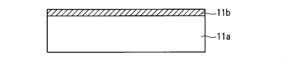
- the semiconductor element 11 has a semiconductor substrate 11a and a wiring electrode 11b electrically connected to the semiconductor substrate 11a.
- the semiconductor element 11 has a back surface (hereinafter referred to as “second main surface”) opposite to the surface (hereinafter referred to as “first main surface”) on which the wiring electrode 11 b is formed (hereinafter referred to as “second main surface”).
- An external output electrode 11c is further provided.
- the semiconductor substrate 11a is made of, for example, SiC.
- SiC is a so-called wide band gap semiconductor.
- a wide bandgap semiconductor has a larger bandgap than Si, and adopting it for the semiconductor substrate 11a is intended to increase the breakdown field strength of the semiconductor element 11 and to keep the semiconductor element 11 at a high temperature of 175 ° C. or higher. This is advantageous from the viewpoint of operation.
- SiC is used as the semiconductor substrate 11a will be described as an example.
- the wiring electrode 11b is realized by any one or a combination of Cu, Al, AlSi, Ni, Au metal layers, for example.
- the back surface external output electrode 11c is realized by any one or a combination of Al, AlSi, Ni, Au metal layers, for example.
- the die bond material 22 for example, a low-temperature sintered material of silver nanoparticles, a liquid phase diffusion bonding material such as Cu—Sn or Ag—Sn, or a bonding material that is a good electrical and thermal conductor such as solder is used. Can do.
- a sintered metal is employed as the die bond material 22 as an example.
- the sintered metal is, for example, sintered Ag.
- the thermal stress generated due to the difference between the thermal expansion coefficient of the semiconductor element 11 and the thermal expansion coefficient of the cooling member 12 during the heat cycle test is absorbed by the semiconductor element 11.
- the die bond material 22 is also bent and stress is generated in the die bond material 22, and the die bond material 22 needs to withstand the stress.
- the thickness of the die bond material 22 is less than 3 ⁇ m, the die bond material 22 cannot withstand the stress generated during the heat cycle test, cracks, and is insufficient in strength. Further, when the die bond material 22 has a thickness exceeding 100 ⁇ m, there is a concern that cracks may occur during the formation process. Therefore, the thickness of the die bond material 22 is preferably 3 ⁇ m or more from the viewpoint of ensuring the strength, and is preferably 100 ⁇ m or less from the viewpoint of preventing the generation of cracks in the formation process.
- a good electrical and thermal conductor such as copper or aluminum can be used.
- the thickness is 0.2 to 1.0 mm and the linear expansion coefficient is 17 ppm.
- the insulating ceramic 6 a ceramic that is an insulator from the electrical viewpoint and that is a good conductor of heat, such as silicon nitride, aluminum nitride, or alumina, can be used.
- silicon nitride is employed for the insulating ceramic 6, for example, the thickness is 0.1 mm to 1.00 mm, and the linear expansion coefficient is 2.5 ppm.
- the overall linear expansion coefficient of the insulating substrate 13 including the conductive plates 5 and 7 can be estimated to be, for example, 5.7 to 8.9 ppm.
- the bonding material 23 for example, a low temperature sintered material of silver nanoparticles, a silver paste material, a liquid phase diffusion bonding material such as Cu-Sn or Ag-Sn, or a bonding material that is a good conductor of heat, such as solder. Can be used.
- solder a bonding material that is a good conductor of heat
- high-strength solder such as Sn—Cu—Sb is preferable.
- the cooling member 12 is formed of a metal material having good heat conduction such as copper or aluminum.
- the thermal resistance from the semiconductor element 11 to the cooling member 12 is small. Therefore, heat generated from the semiconductor element 11 is transmitted to the cooling member 12 with excellent heat transferability. Further, most of the thermal stress resulting from the difference between the thermal expansion coefficient of the semiconductor element 11 and the thermal expansion coefficient of the cooling member 12 is absorbed by the plastic deformation of the semiconductor element 11. Therefore, the reliability of joining between the insulating substrate 13 and the cooling member 12 is sufficiently ensured.
- FIGS. 2 to 5 are cross-sectional views sequentially showing the manufacturing process of the semiconductor element 11.
- a device surface is formed on the first main surface.
- the device surface is, for example, a source side surface in a MOSFET.
- the wiring electrode 11b is formed (see FIG. 2).
- the second main surface is ground so that the thickness of the semiconductor substrate 11a is, for example, 50 ⁇ m or more and 100 ⁇ m or less (see FIG. 3).
- the grinding can be realized, for example, with a grinding machine that employs a grindstone in which diamond abrasive grains are combined by vitrification.
- a protective tape is attached to the first main surface side of the semiconductor substrate 11a to protect the device surface from grinding.
- the device surface may be protected by applying wax or the like to the first main surface and attaching a support substrate.
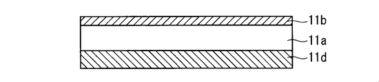
- a metal film 11d for forming silicide is deposited on the second main surface (see FIG. 4).
- An example of the material of the metal film 11d is Ni.
- the metal film 11d and the semiconductor substrate 11a are reacted to form a silicide layer, thereby forming a contact electrode. This reaction is realized by irradiating the metal film 11d with laser light.
- the surface of the contact electrode is etched to remove the oxide film and the like on the surface. Etching can be realized, for example, by dry etching using Ar + ions. At this time, a part of the unreacted metal film 11d may remain.
- a back external output electrode 11c is formed on the surface of the contact electrode (see FIG. 5).
- the illustration of the contact electrode is omitted.
- the film formation method of the backside external output electrode 11c greatly affects its adhesion.
- the back surface external output electrode 11c is formed by DC sputtering. The film formation temperature became 100 ° C. or higher by the electric power supplied at this time.
- FIGS. 2 to 5 are views focusing on one of the plurality of semiconductor elements 11 manufactured in parallel.
- the semiconductor wafer is used as a semiconductor substrate 11 a in a plurality of semiconductor elements 11.
- a plurality of them are connected via the semiconductor substrate 11a, so that each of the semiconductor elements 11 is obtained by dicing.
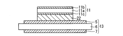
- FIG. 6 is a cross-sectional view showing a process before the semiconductor device 101 is obtained after each of the semiconductor elements 11 is manufactured.
- An insulating substrate 13 in which the conductive plates 5 and 7 and the insulating ceramic 6 are integrated in advance as described above is prepared.
- the semiconductor element 11 is bonded to the conductive plate 5 on the second main surface side through the die bond material 22.
- the cooling member 12 is joined to the conductive plate 7 via the joining material 23.
- the semiconductor device 101 is manufactured (see FIG. 1). That is, this manufacturing process contributes to the manufacture of the semiconductor device 101.
- the semiconductor device 101 bends due to the difference between the linear expansion coefficient of the cooling member 12 that is a good conductor of heat and the linear expansion coefficients of the insulating substrate 13 and the semiconductor element 11. Therefore, the greater the deflection, the greater the stress generated in the die bond material 22.
- the cooling member 12 is directly connected to the bonding material 23 employing, for example, solder.
- the cooling member 12 is bonded to the insulating substrate 13 to which the semiconductor element 11 is die-bonded via the bonding material 23. Therefore, bending due to the difference between the linear expansion coefficient of the cooling member 12 and the linear expansion coefficients of the insulating substrate 13 and the semiconductor element 11 is likely to occur.
- a base plate (not shown) made of a copper material is joined to the cooling member 12 via grease. Further, an insulating substrate 13 to which the semiconductor element 11 is die-bonded is bonded to the base plate through a bonding material employing, for example, solder. Therefore, the bending due to the difference between the linear expansion coefficient of the cooling member 12 and the linear expansion coefficients of the insulating substrate 13 and the semiconductor element 11 is alleviated by the grease and the base plate, and the bending is alleviated compared to the direct cooling type module structure. The That is, the stress generated in the die bond material 22 is reduced.
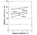
- FIG. 7 is a graph showing the relationship of the lifetime of the die bond material 22 to the overall linear expansion coefficient of the insulating substrate 13 bonded to the semiconductor element 11 via the die bond material 22 in the semiconductor device 101.
- the thickness t of the semiconductor element 11 is adopted as an auxiliary variable in this relationship, and the values are shown as 100 ⁇ m, 200 ⁇ m, and 300 ⁇ m.
- CAE Computer Aided Design
- 7 indicates the linear expansion coefficient of the insulating substrate 13 as a whole (in the drawing, simply expressed as “linear expansion coefficient of the insulating substrate 13”: the same applies hereinafter) in units of ppm. 7 indicates the life of the die bond material 22, that is, the number of cycles of the heat cycle test until the die bond material 22 fails when the heat cycle test is performed.
- the heat cycle test here is a temperature cycle test in which the external environment temperature of the semiconductor device 101 is changed from ⁇ (minus) 40 ° C. to 175 ° C. to ⁇ (minus) 40 ° C. again.
- the linear expansion coefficient is 23 ppm
- the linear expansion coefficient of the semiconductor element 11 using SiC is 4.6 ppm. I will explain to you.
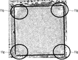
- FIG. 8 is a Scanning Acoustic Tomograph (SAT) image showing the peeling that occurred on the die bond material 22. This peeling is caused by a heat cycle test.
- This SAT image is the semiconductor device 101 viewed from the first main surface side of the semiconductor element 11. In the region 11g of the corner portion of the semiconductor element 11, a white portion indicating a peeled state is visible. Since the depth position of the SAT image is set at the position of the die bond material 22, this portion reflects the peeled state of the die bond material 22. From the viewpoint of improving the number of heat cycles until such peeling of the die bond material 22 occurs, it is desirable to reduce the thickness t of the semiconductor element 11.
- the heat cycle life is about 3000 to 7000 cycles
- the heat cycle life is about 400 to 600 cycles
- the heat cycle life is about 200 to 300 cycles. That is, when the thickness t is 100 ⁇ m, the heat cycle life of the die bond material 22 is improved by about one digit as compared with the case where the thickness t is 200 ⁇ m and 300 ⁇ m. On the other hand, when the thickness t is 200 ⁇ m, the heat cycle life of the die bond material 22 is improved only about twice as compared with the case where the thickness t is 300 ⁇ m.
- the thickness t of the semiconductor element 11 is desirably 100 ⁇ m or less.
- the thickness t is desirably 50 ⁇ m or more. Therefore, it can be said that the desirable range of the thickness t of the semiconductor element 11 is 50 ⁇ m or more and 100 ⁇ m or less (that is, 0.05 mm or more and 0.1 mm or less).
- the semiconductor element 11 In order for the semiconductor element 11 to follow the bending of the cooling member 12, the semiconductor element 11 must withstand the stress applied to itself. Therefore, next, a desirable bending strength range in the semiconductor element 11 will be described.
- the bending strength of the semiconductor element 11 is desirably 700 MPa or more.
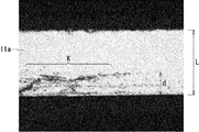
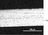
- the bending strength of the semiconductor element 11 depends on the manufacturing process of the semiconductor element 11 and its thickness t. Among them, a dicing condition for the semiconductor element 11 is particularly important. 9 and 10 are both cross-sectional images of the semiconductor element 11 after dicing by a microscope. However, the sample of FIG. 9 and the sample of FIG. 10 have different dicing conditions.
- Fig. 10 no cracks are observed.
- the number of elements that trigger breakage is reduced when the bending strength is evaluated. That is, the workability of the semiconductor device 101 employing the semiconductor element 11 is excellent. Therefore, the sample of FIG. 10 is more preferable than the sample of FIG. 9 from the viewpoint of improving the bending strength.
- the improvement of the dicing conditions can be obtained by appropriately selecting the type and thickness of the blade used for dicing, the type of the dicing tape itself, and the type of the adhesive for the dicing tape.
- the thickness of the blade is desirable to reduce. This is because excessive cracks generated during dicing are reduced. It is also desirable to increase the adhesive strength of the dicing tape adhesive. This is to prevent the object (here, the semiconductor element 11) from being deformed by the stress generated during the blade.
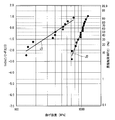
- FIG. 11 is a graph showing the relationship between the cumulative failure rate of the semiconductor element 11 and the bending strength, and shows a so-called Weibull plot.
- the right vertical axis shows the cumulative failure rate F (t) of the semiconductor element 11 as a percentage
- the left vertical axis shows the value ln (ln (1 / (1-F (t)))) (where the symbol ln is the natural logarithm).
- symbol t in symbol F (t) indicates time).
- the horizontal axis of FIG. 11 shows the bending strength of the semiconductor element 11 by adopting MPa as a unit.
- FIG. 11 shows the regression lines J1 and J2 for the semiconductor element 11 manufactured under different first and second dicing conditions.
- the blade thickness is smaller in the second dicing condition than in the first dicing condition, and the adhesive strength of the adhesive of the dicing tape is stronger.
- the semiconductor element 11 manufactured under the first dicing condition has a bending strength of about 100 to 800 MPa as indicated by the regression line J1.
- the semiconductor element 11 manufactured under the second dicing condition has a bending strength of about 700 to 1100 MPa as indicated by the regression line J2.
- the variation in bending strength is smaller in the second dicing condition than in the first dicing condition.
- FIG. 12 is a graph showing stress in the thickness direction (vertical stress) applied to the semiconductor element 11 in the semiconductor device 101.
- the graph shows the result of calculation performed by CAE (Computer Aided Design).
- the value of the stress applied to the semiconductor element 11 is adopted on the vertical axis, and the value of the linear expansion coefficient of the insulating substrate 13 bonded to the semiconductor element 11 via the die bonding material 22 is adopted on the horizontal axis.
- the thickness t of the semiconductor element 11 was used as an auxiliary variable, and 100 ⁇ m, 200 ⁇ m, and 300 ⁇ m were adopted as the value.
- the stress value applied to the semiconductor element 11 is less than 400 MPa at any thickness t of the semiconductor element 11 with respect to the linear expansion coefficient of the insulating substrate 13. Therefore, if the bending strength of the semiconductor element 11 is less than 400 MPa, the semiconductor element 11 is cracked, and if this is 400 MPa or more, it is considered that no defect occurs in the semiconductor element 11.
- the calculation results in FIG. 12 are consistent with the semiconductor element 11 having a bending strength of 700 MPa or more in that there is no defect exemplified by cracking even if the heat cycle test is performed 1000 cycles.
- the thinner the thickness t the higher the stress applied to the semiconductor element 11. That is, the thinner the thickness t, the higher the bending strength of the semiconductor element 11 is required.
- the heat cycle life of the die bond material 22 is improved as the thickness t is decreased.
- the thickness t of the semiconductor element 11 that obtained the cumulative failure rate F (t) related to the graph of FIG. 11 was 100 ⁇ m. Therefore, in consideration of manufacturing variations, the bending strength of the semiconductor element 11 is more preferably 1000 MPa or more.
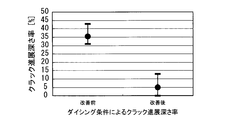
- FIG. 13 is a graph showing the relationship between dicing conditions and crack growth depth rate.
- the crack growth depth ratio indicates the size of a crack entering the chip end face after dicing.
- the crack growth depth rate is defined as a percentage of the ratio of the crack depth d to the chip thickness L (100 ⁇ d / L [%]) with reference to FIG.
- “before improvement” and “after improvement” correspond to the first dicing condition and the second dicing condition, respectively.
- FIG. 13 shows that the crack growth depth rate is lower in the second dicing condition than in the first dicing condition. It can be seen from FIG. 11 that the crack growth depth ratio exceeds 30% under the first dicing condition that caused a decrease in strength. From this, it can be seen that in order to improve the strength, it is necessary to suppress the crack growth depth ratio to 30% or less.
- the semiconductor device 101 absorbs the thermal stress caused by the difference between the linear expansion coefficient of the semiconductor element 11 and the thermal expansion coefficient of the cooling member 12 by the semiconductor element 11. Therefore, the stress generated in the bonding material 23 can be relaxed. Therefore, the semiconductor device 101 having high thermal conductivity and excellent workability and reliability can be obtained. In addition, since the lower limit of the thickness of the semiconductor element 11 does not deteriorate the yield in the manufacturing process of the semiconductor element 11, there is no significant increase in cost.
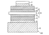
- FIG. 14 is a cross-sectional view showing the structure of the semiconductor device 102 according to this embodiment.
- the semiconductor device 102 has a configuration in which the insulating substrate 13 is replaced with an insulating substrate 14 with respect to the structure of the semiconductor device 101 in the first embodiment.
- Other components are the same as those of the semiconductor device 101.
- the semiconductor element 11 the distinction between the semiconductor substrate 11a, the wiring electrode 11b, and the back surface external output electrode 11c is omitted.
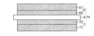
- the insulating substrate 14 includes insulating ceramics 6, copper plates 51 and 71, and aluminum plates 52 and 72.
- the copper plates 51 and 71 are made of copper.
- the aluminum plates 52 and 72 are made of aluminum.
- Aluminum plates 52 and 72 are provided in contact with insulating ceramic 6, copper plate 51 is provided in contact with aluminum plate 52, and copper plate 71 is provided in contact with aluminum plate 72.
- the aluminum plate 52 is sandwiched between the insulating ceramic 6 and the copper plate 51, and the aluminum plate 72 is sandwiched between the insulating ceramic 6 and the copper plate 71.
- the copper plate 51 is bonded to the semiconductor element 11 via the die bond material 22, and the copper plate 71 is bonded to the cooling member 12 via the bonding material 23.
- the copper plate 51 and the aluminum plate 52 can be collectively grasped as the conductive plate 5 according to the first embodiment.
- the copper plate 71 and the aluminum plate 72 can be collectively grasped as the conductive plate 7 according to the first embodiment.
- the conductive plate 7 is made of a laminated structure of copper having high thermal conductivity and aluminum that is easily plastically deformed, so that the insulating substrate 14 and the cooling are compared with the case where the conductive plate 7 is made of only copper.
- the reliability of the joint with the member 12 is improved. This is suitable when the cooling member 12 is made of aluminum. This is because thermal stress is equalized between the members on both sides of the bonding material 23, that is, the cooling member 12 and the conductive plate 7. In particular, when the bonding material 23 is made of solder, the effect is remarkable.
- the aluminum plate 72 is pure aluminum having a purity of at least 99.5% or more, preferably 99.9% or more.
- the linear thermal expansion coefficient of the insulating substrate 14 as a whole can be brought close to the linear thermal expansion coefficient of aluminum, and the stress acting on the bonding material 23 can be reduced.
- Such reduction in stress is desirable from the viewpoint of improving the reliability of bonding between the insulating substrate 14 and the cooling member 12.
- the aluminum plate 52 is also pure aluminum having a purity of at least 99.5% or more, preferably 99.9% or more. It is desirable.
- an insulating substrate 14 is prepared.
- “preparing” refers to preparing an insulating substrate 14 having insulating ceramics 6 as insulating plates and conductive plates 5 and 7 provided on both surfaces of the insulating ceramics 6. Does not mean manufacturing.
- a cooling member 12 is also prepared.
- FIG. 16 shows a step of disposing the semiconductor element 11 on the insulating substrate 14 (more specifically, on the copper plate 51) via the die bonding material 22. Thereafter, the cooling member 12 is further bonded to the copper plate 71 on the opposite side of the insulating substrate 14 from the side on which the semiconductor element 11 is disposed via the bonding material 23, and the configuration shown in FIG. 14 is obtained. It is done.
- FIG. 17 is a cross-sectional view showing the structure of the semiconductor device 103 according to this embodiment.
- the semiconductor device 103 is realized by configuring the backside external output electrode 11c and the conductive plate 5 with copper and omitting the die bonding material 22 from the semiconductor device 101 according to the first embodiment. That is, the back surface external output electrode 11c and the conductive plate 5 are joined to each other without the die bonding material 22 interposed therebetween. Other configurations are the same as those of the semiconductor device 101.
- the back surface external output electrode 11c and the conductive plate 5 are bonded by liquid phase diffusion bonding or solid phase diffusion bonding. Bonding in this manner improves resistance to stress. This improves the reliability of the junction between the insulating substrate 13 and the semiconductor element 11.
- FIG. 18 is a cross-sectional view showing the structure of another semiconductor device 104 according to this embodiment.
- the semiconductor device 104 is realized by configuring the back surface external output electrode 11c from copper and omitting the die bonding material 22 from the semiconductor device 102 according to the second embodiment. That is, the back surface external output electrode 11c and the copper plate 51 are bonded to each other without the die bonding material 22 interposed therebetween.
- Other configurations are the same as those of the semiconductor device 102.
- the back surface external output electrode 11c and the copper plate 51 are bonded by liquid phase diffusion bonding or solid phase diffusion bonding. Bonding in this manner improves resistance to stress. This improves the reliability of the junction between the insulating substrate 14 and the semiconductor element 11.
- the semiconductor element 11 and the insulating substrate 13 or the semiconductor element 11 are insulated.
- the substrate 14 can be bonded by solid phase diffusion bonding or liquid phase diffusion bonding.
- both the back surface external output electrode 11c and the conductive plate 5 are made of copper.
- the conductive plate 7 may also be made of copper.
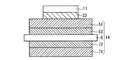
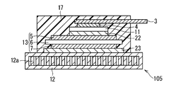
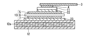
- FIG. 19 is a cross-sectional view showing the structure of the semiconductor device 105 according to this embodiment.
- the semiconductor device 105 has a configuration in which a lead 3, a bonding material 4, and a sealing resin 17 are added to the semiconductor device 101 described in the first embodiment.
- the cooling member 12 has a shape having the radiation fins 12a.
- the semiconductor element 11 the distinction between the semiconductor substrate 11a, the wiring electrode 11b, and the back external output electrode 11c is omitted.
- the bonding material 4 is bonded to the semiconductor element 11 (that is, to the first main surface) on the side opposite to the die bonding material 22, and the lead 3 is bonded to the semiconductor element 11 via the bonding material 4.
- the sealing resin 17 is provided on the cooling member 12 and seals the lead 3, the bonding material 4, the semiconductor element 11, the insulating substrate 13, the die bonding material 22, and the bonding material 23.
- the semiconductor device 105 having such a configuration can be operated at a temperature exceeding 175 ° C. by adopting SiC as the base material of the semiconductor element 11.
- the semiconductor device 105 can be reduced in size, and versatility is increased. For example, when an inverter is configured using the semiconductor device 105, this contributes to downsizing the inverter.
- FIG. 20 to 22 are cross-sectional views sequentially showing the manufacturing process of the semiconductor device 105 according to the present embodiment.
- an insulating substrate 13 in which the conductive plates 5 and 7 and the insulating ceramic 6 are integrated in advance is prepared.
- the 2nd main surface side of the semiconductor element 11 is joined to the conducting plate 5 through the die-bonding material 22 (refer FIG. 20).
- the cooling member 12 is joined to the conductive plate 7 via the joining material 23 (see FIG. 21).
- the bonding material 4 is bonded to the first main surface side of the semiconductor element 11, and the lead 3 is bonded to the bonding material 4 from the side opposite to the semiconductor element 11 with respect to the bonding material 4 (see FIG. 22).
- a sealing resin 17 is provided.
- the manufacturing process shown in FIG. 14 is obtained. In other words, this manufacturing process contributes to the realization of the semiconductor device 105.
- the respective embodiments can be freely combined, arbitrary constituent elements of the respective embodiments are appropriately modified, or arbitrary constituent elements are omitted in the respective embodiments. It is possible to
Abstract
熱伝導性が高く、かつ、工作性に優れた半導体装置を提供する。半導体装置101は、絶縁基板13と、半導体素子11と、ダイボンド材22と、接合材23と、冷却部材12とを備える。絶縁基板13は、絶縁セラミックス6と、絶縁セラミックス6の一方の面に設けられた導板5と、他方の面に設けられた導板7とを有する。半導体素子11は導板5上にダイボンド材22を介して設けられる。ダイボンド材22には焼結金属が採用される。半導体素子11はその曲げ強度が700MPa以上であり、厚さが0.05mm以上0.1mm以下である。冷却部材12は導板7に接合材23を介して接合される。
Description
本発明は、半導体装置およびその製造方法に関するものである。
パワーモジュールに採用される半導体装置には、例えばSi(珪素)あるいはSiC(炭化珪素)を基材とする半導体素子が使用される。半導体素子の温度を所定温度以下に保つ必要から、半導体素子から発せられる熱を効率良く放熱することが望まれる。
この放熱という観点で、従来から、半導体素子に対して絶縁基板を介して冷却器が接合されたパワーモジュールが提案されている。絶縁基板では、高熱伝導性の絶縁セラミック板と、その両面に設けられた高熱伝導性の金属からなる導板とが一体となっている。絶縁セラミック板には、例えば窒化珪素、窒化アルミニウムまたはアルミナが用いられる。導板には、例えばアルミニウム(アルミニウム合金を含む。以下、同じ)または銅(銅合金を含む。以下、同じ)が用いられる。
絶縁基板の一方の面には、半導体素子が、焼結Ag等の焼結金属を介して接合される。絶縁基板の他方の面には、半田等の接合材を介して直接的または間接的に冷却器が接合される。
他方、半導体装置を封止する樹脂の変形を抑制する観点で、半導体素子についての提案もされている。かかる変形は、例えば外部環境の温度変化に由来する。例えばその曲げ強度が100MPa以上1000MPa以下の半導体素子が、応力緩和部材として配置される。
特許文献1における応力緩和部材は、絶縁基板の主面に配置された100MPa以上1000MPa以下の曲げ強度を有する半導体素子からなる。
放熱という観点に関して上述のように提案された構成であっても、当該構成に要求される寿命期間において十分な放熱性能を維持できない場合があった。これは半導体素子と冷却器とではそれぞれの熱膨張係数が相違し、使用条件によっては熱応力が発生すること、その熱応力により半導体素子あるいは、半導体素子と冷却器との間の接合部材に、クラックが生じること、が原因である。
例えば特許文献1に開示された応力緩和部材を備える半導体装置には、冷却器と絶縁基板とが半田で直接に接合されている直接冷却式モジュールにおいて、問題点がある。絶縁基板上には半導体素子(例えばSiCチップ)と接合されているAgシンター部が存在する。一般にSiCはSiよりも高いジャンクション温度に耐えることが期待されており、高温/低温を繰り返すヒートサイクルは、その高温時において175℃以上となる。そしてかかるヒートサイクルで動作する際、このAgシンター部にクラックが生じる場合があった。
本発明は、上記のような問題を解決するためになされたものであり、熱伝導性が高く、かつ、工作性に優れた半導体装置、およびその製造方法を提供することを目的とする。
この発明にかかる半導体装置は、絶縁板と、前記絶縁板の一方の面に設けられた第1の導板と、前記絶縁板の他方の面に設けられた第2の導板とを有する絶縁基板を備える。更に、焼結金属と、前記焼結金属を介して前記第1の導板上に設けられた厚さ0.05mm以上0.1mm以下である半導体素子と、接合材と、前記接合材を介して前記第2の導板に接合された冷却部材とを備える。前記半導体素子の曲げ強度は700MPa以上である。あるいは前記半導体素子は、そのチップ厚みの30%以下のクラック進展深さ率を有する。
この発明にかかる半導体装置の製造方法は、(a)絶縁板と、前記絶縁板の一方の面に設けられた第1の導板と、前記絶縁板の他方の面に設けられた第2の導板とを有する絶縁基板を用意する工程と、(b)前記第1の導板に、焼結金属を介して半導体素子を設ける工程と、(c)前記第2の導板に、第1の接合材を介して冷却部材を接合させる工程とを備える。
この発明にかかる半導体装置によれば、半導体素子の線膨張係数と、冷却部材の熱膨張係数との差に起因する熱応力が、半導体素子で吸収される。よって熱伝導性を高くしつつも、接合材に発生する応力を緩和し、工作性に優れる。この発明にかかる半導体装置の製造方法は、この発明にかかる半導体装置の製造に資する。
この発明の目的、特徴、局面、および利点は、以下の詳細な説明と添付図面とによって、より明白となる。
<実施の形態1>.
図1は、実施の形態1にかかる半導体装置101の構造を示す断面図である。半導体装置101は、半導体素子11、ダイボンド材22、絶縁基板13、接合材23、冷却部材12を備えている。
図1は、実施の形態1にかかる半導体装置101の構造を示す断面図である。半導体装置101は、半導体素子11、ダイボンド材22、絶縁基板13、接合材23、冷却部材12を備えている。
半導体素子11は、ダイボンド材22を介して絶縁基板13の一方の面に接合されている。絶縁基板13の他方の面と冷却部材12とが、接合材23を介して接合されている。絶縁基板13は、絶縁板としての絶縁セラミックス6と、絶縁セラミックス6の一方の面に設けられた導板5と、他方の面に設けられた導板7とを有する。換言すれば絶縁基板13は、導板5,7と、導板5と導板7とに挟まれて配置された絶縁セラミックス6とを有する。これらはろう材等を用いてあらかじめ絶縁基板13として一体化されている。
導板5はダイボンド材22に接する。よって半導体素子11はダイボンド材22を介して導板5上に設けられ、より具体的には導板5に接合される。但し、半導体素子11と絶縁基板13とがCu固相拡散接合または超音波接合等の直接接合で接合されて、ダイボンド材22が省略されてもよい。導板7は冷却部材12に対向し、接合材23を介して冷却部材12に接合される。
半導体素子11は半導体基体11aと、半導体基体11aに電気的に接続された配線電極11bとを有する。半導体素子11は、配線電極11bが形成された面(以下「第1主面」と称す)とは反対側(図中下側)の面(以下「第2主面」と称す)に、裏面外部出力電極11cを更に有する。
半導体基体11aは例えばSiCを基材とする。SiCは、いわゆるワイドバンドギャップ半導体である。ワイドバンドギャップ半導体はSiに比べてバンドギャップが大きく、これを半導体基体11aに採用することは、半導体素子11の絶縁破壊電界強度を大きくする観点で、また半導体素子11を175℃以上の高温で動作させる観点で有利である。以下、半導体基体11aとしてSiCを基材とする場合を例にとって説明する。
配線電極11bは、例えばCu、Al、AlSi、Ni、Auの金属層のいずれかまたはその組み合わせで実現される。本実施の形態において、裏面外部出力電極11cは、例えばAl、AlSi、Ni、Auの金属層のいずれかまたはその組み合わせで実現される。
ダイボンド材22には、例えば銀ナノ粒子の低温焼結材、Cu-SnまたはAg-Snのような液相拡散接合材、または、半田等の、電気および熱の良導体である接合材料を用いることができる。以下ではダイボンド材22として焼結金属を採用する場合を例に取って説明する。当該焼結金属は例えば焼結Agである。
ヒートサイクル試験時に半導体素子11の熱膨張係数と冷却部材12の熱膨張係数との差に起因して発生する熱応力は、半導体素子11で吸収される。半導体装置101全体が撓むときに、ダイボンド材22も撓んでダイボンド材22に応力が発生し、ダイボンド材22はその応力に耐える必要がある。
ダイボンド材22は、その厚みが3μm未満であるとヒートサイクル試験時に発生する応力に耐えることができず、クラックが入り、強度的に不十分である。またダイボンド材22は、その厚みが100μmを超えると、その形成プロセス中にクラックが入る懸念がある。よってダイボンド材22の厚さは、その強度を確保する観点で3μm以上であることが望ましく、形成プロセスでクラックが発生することを防止する観点で100μm以下であることが望ましい。
導板5,7のいずれにも、例えば銅またはアルミニウム等の電気および熱の良導体を用いることができる。導板5,7に銅を採用した場合、例えば、その厚みが0.2~1.0mmであり、線膨張係数は17ppmである。
絶縁セラミックス6には、窒化珪素、窒化アルミニウムまたはアルミナ等の、電気的観点で絶縁体であり、かつ、熱の良導体であるセラミックスを用いることができる。絶縁セラミックス6に窒化珪素を採用した場合、例えばその厚みが0.1mm~1.00mmであり、線膨張係数は2.5ppmである。また上記導板5,7を合わせた絶縁基板13の全体としての線膨張係数は例えば5.7~8.9ppmと見積もることができる。
接合材23には、例えば銀ナノ粒子の低温焼結材、銀ペースト材、Cu-SnまたはAg-Snのような液相拡散接合材、または、半田等の、熱の良導体である接合材料を用いることができる。半田で接合する場合は、半田材の降伏応力も留意することが望ましく、例えばSn-Cu-Sbのような高強度半田が好ましい。
冷却部材12は、銅またはアルミニウムなどの熱伝導の良好な金属材料で形成される。
このような構成によれば、半導体素子11から冷却部材12までの熱抵抗は小さい。従って半導体素子11からの発熱は冷却部材12まで優れた熱伝達性によって伝達される。また、半導体素子11の熱膨張係数と冷却部材12の熱膨張係数との相違に起因する熱応力は、半導体素子11の塑性変形によって大部分が吸収される。よって絶縁基板13と冷却部材12との間の接合の信頼性が十分に確保される。
次に、図2から図5を用いて、半導体素子11の製造工程、特に半導体素子11の厚さtが100μm以下の場合の製造工程を簡単に例示する。図2から図5は、半導体素子11の製造工程を順次に示す断面図である。まず第1主面にデバイス面を作製する。当該デバイス面は、例えばMOSFETではソース側の面である。この工程において配線電極11bが形成される(図2参照)。
次に、第2主面を研削し、半導体基体11aの厚さを例えば50μm以上100μm以下にする(図3参照)。当該研削は、例えば、ダイヤモンド砥粒をビトリファイドで結合した砥石を採用した研削機で実現できる。当該研削の際には、半導体基体11aの第1主面側に保護テープを貼り付けて、デバイス面を研削から保護する。あるいは第1主面にワックスなどを塗布し、サポート基板を貼り付けてデバイス面を保護してもよい。
研削の後、第2主面にシリサイドを形成するための金属膜11dを堆積する(図4参照)。金属膜11dの材料として例えばNiが挙げられる。その後、金属膜11dと半導体基体11aとを反応させてシリサイド層を形成し、コンタクト電極を形成する。当該反応は金属膜11dへのレーザ光の照射で実現される。
その後、コンタクト電極の表面に対してエッチングを行い、当該表面の酸化膜等を除去する。エッチングは例えばAr+イオンを用いたドライエッチングで実現できる。この際、未反応の金属膜11dの一部が残っても構わない。
表面の酸化膜が除去された後、コンタクト電極の表面上に、裏面外部出力電極11cを形成する(図5参照)。簡単のため、コンタクト電極の図示は省略した。裏面外部出力電極11cの成膜方法はその密着性に大きく影響する。本実施の形態では、DCスパッタによって裏面外部出力電極11cの成膜を行った。この際に投入した電力により、成膜温度は100℃以上となった。
通常、半導体素子11は、その複数が同じ半導体ウェハにおいて製造される。よって図2から図5に示された工程は、並行して製造される複数の半導体素子11の一つについて着目した図である。当該半導体ウェハは複数の半導体素子11において半導体基体11aとして用いられる。半導体素子11の製造が完了した直後は、それらの複数同士が半導体基体11aを介して繋がっているので、ダイシングにより半導体素子11の各々が分離して得られる。
図6は半導体素子11の各々を製造した後、半導体装置101を得る前の工程を示す断面図である。導板5,7と絶縁セラミックス6とが上述の様に予め一体化した絶縁基板13を用意する。そして導板5に、半導体素子11をその第2主面側で、ダイボンド材22を介して接合する。他方、導板7に接合材23を介して冷却部材12を接合する。このようにして半導体装置101が製造される(図1参照)。つまりかかる製造工程は、半導体装置101の製造に資する。
一般に、ヒートサイクル試験により、熱の良導体である冷却部材12の線膨張係数と、絶縁基板13および半導体素子11の線膨張係数との違いにより、半導体装置101には撓みが発生する。よってこの撓みが大きいほど、ダイボンド材22に発生する応力が大きくなる。
本実施の形態で用られる直接冷却式モジュール構造では、冷却部材12は、例えば半田が採用される接合材23が直接に接続される。そして冷却部材12は、半導体素子11をダイボンドした絶縁基板13に対して、接合材23を介して接合される。よって、冷却部材12の線膨張係数と、絶縁基板13および半導体素子11の線膨張係数との差に起因した撓みが発生しやすくなる。
通常のモジュール構造では、冷却部材12に、銅材でできたベース板(図示省略)を、グリスを介して接合する。さらにベース板には、例えば半田が採用される接合材を介して、半導体素子11をダイボンドした絶縁基板13が接合される。よって冷却部材12の線膨張係数と、絶縁基板13および半導体素子11の線膨張係数との差に起因した撓みが、グリスやベース板により緩和され、直接冷却式モジュール構造に比べて撓みが緩和される。つまりダイボンド材22に発生する応力は小さくなる。
次に、ダイボンド材22に発生する応力を低減させるために望ましい絶縁基板13の線膨張係数を求めるための計算を示す。
図7は、半導体装置101において、半導体素子11とダイボンド材22を介して接合される絶縁基板13の全体としての線膨張係数に対する、ダイボンド材22の寿命の関係を示すグラフである。この関係における助変数として半導体素子11の厚さtを採用し、その値が100μm,200μm,300μmの場合を示した。但し、これらのグラフはいずれも、CAE(コンピュータ支援設計)により行った解析結果である。またダイボンド材22として焼結Agを用い、これを介して絶縁基板13が半導体素子11と接合され、接合材23を介して絶縁基板13に冷却部材12が接合された場合を例示した。
図7の横軸は、絶縁基板13の全体としての線膨張係数(図では単に「絶縁基板13の線膨張係数」と表記:以下同様)を単位ppmにて示す。また図7の縦軸はダイボンド材22の寿命、つまりヒートサイクル試験を行った際にダイボンド材22が故障するまでのヒートサイクル試験のサイクル数を示す。ここでのヒートサイクル試験は、半導体装置101の外部環境温度を-(マイナス)40℃度から175℃を経て再び-(マイナス)40℃に変化させる温度サイクル試験である。
直接冷却式モジュール構造で用いている冷却部材12をAlで構成する場合を想定してその線膨張係数を23ppmとし、SiCを用いた半導体素子11の線膨張係数を4.6ppmとした場合を例にとって説明する。
絶縁基板13の線膨張係数が大きいほど、これと冷却部材12の線膨張係数との差は小さく、絶縁基板13と冷却部材12との間に位置する接合材23に発生する応力は小さい。しかし絶縁基板13の線膨張係数が大きいほど、絶縁基板13の線膨張係数と半導体素子11の線膨張係数との差は大きく、絶縁基板13の撓みによってダイボンド材22に発生する応力は大きい。よって絶縁基板13の線膨張係数が大きいほどダイボンド材22の寿命は短い。
逆に絶縁基板13の線膨張係数が小さいほど、冷却部材12の撓みによって接合材23に発生する応力は大きく、ダイボンド材22に発生する応力は小さく、ダイボンド材22の寿命は長い。
ダイボンド材22の寿命改善に限って言えば、たとえば半導体素子11にSiCを用いた場合にその線膨張係数は4.6ppmであり、絶縁基板13の線膨張係数は4.6ppmに近いほど良好である。ただし、冷却部材12が例えばAlで構成される場合、その線膨張係数は23ppmであるので、絶縁基板13の線膨張係数が半導体素子11の線膨張係数に近いほど、絶縁基板13の線膨張係数と冷却部材12の線膨張係数との差が大きく、冷却部材12の撓みによって接合材23に発生する応力は大きくなる。
接合材23に影響を与えない範囲で試算すると、図7に示すように、絶縁基板13の線膨張係数の相違がダイボンド材22のヒートサイクル寿命に与える影響は小さい。
図7で示された絶縁基板13の線膨張係数のいずれにおいても、半導体素子11の厚さtを薄くすることにより、ダイボンド材22の寿命が改善されることが分かる。これは半導体素子11は、その厚みが薄いほど、冷却部材12の撓みに追従し易く、以てダイボンド材22に発生する応力を緩和させ得るからであると考えられる。よって半導体装置101において半導体素子11の厚みを薄くすることは、ダイボンド材22の寿命を改善する観点で望ましい。
図8はダイボンド材22に発生した剥離を示すScanning Acoustic Tomograph(SAT)像である。この剥離はヒートサイクル試験により発生したものである。このSAT像は、半導体装置101を半導体素子11の第1主面側から見たものである。半導体素子11のコーナー部の領域11gにおいて、剥離状態を示す白い部分が見えている。SAT像の深さ位置をダイボンド材22に位置に設定しているので、この部分はダイボンド材22の剥離状態を反映している。このようなダイボンド材22の剥離が発生するまでのヒートサイクル数を向上させる観点で、半導体素子11の厚さtを薄くすることが望ましい。
図7から理解されるように、厚さtが100μmの場合はヒートサイクル寿命が約3000~7000サイクルであり、厚さtが200μmの場合はヒートサイクル寿命が約400~600サイクルであり、厚さtが300μmの場合はヒートサイクル寿命が約200~300サイクルである。つまり厚さtが100μmの場合は、厚さtが200μmの場合および300μmの場合と比較すると、ダイボンド材22のヒートサイクル寿命は1桁程度向上している。これに対して、厚さtが200μmの場合は、厚さtが300μmの場合と比較すると、ダイボンド材22のヒートサイクル寿命は2倍程度しか向上していない。
よってヒートサイクル寿命を顕著に向上させる観点から、半導体素子11の厚さtは100μm以下であることが望ましい。他方、製造プロセスでの歩留まりを考慮すると、厚さtは50μm以上であることが望ましい。従って半導体素子11の厚さtの望ましい範囲は50μm以上100μm以下(即ち0.05mm以上0.1mm以下)であると言える。
半導体素子11が冷却部材12の撓みに追従するには、半導体素子11が自身に印加される応力に耐えなければならない。そこで、次に、半導体素子11において望ましい曲げ強度の範囲について説明する。
図7に関して説明したヒートサイクル試験を半導体素子11に対して行った場合、例えば1000サイクルのヒートサイクル試験では、100~700MPa未満の曲げ強度を有する半導体素子11では、そのチップのエッジ部分からの割れが発生した。他方、700MPa以上の曲げ強度を有する半導体素子11では、かかる割れは発生しなかった。よって半導体素子11の曲げ強度は700MPa以上であることが望ましい。
半導体素子11の曲げ強度は、半導体素子11の製造過程およびその厚さtに依存する。その中でも特に重要なパラメータとして半導体素子11のダイシング条件があげられる。図9および図10はいずれもダイシング後の半導体素子11の顕微鏡による断面像である。但し図9の試料と図10の試料とはダイシング条件が異なっている。
図9ではエッジ部にクラックKが観察される。クラックKの存在により、曲げ強度の評価の際にこれが引き金となって割れやすくなる。よってクラックKの存在は、曲げ強度の向上という観点で望ましくない。
図10ではクラックは観察されない。このような半導体素子11は曲げ強度の評価の際に、破壊の引き金になる要素が減少する。つまり半導体素子11を採用する半導体装置101の工作性に優れる。よって曲げ強度の向上という観点で、図10の試料の方が、図9の試料よりも望ましい。
つまり、クラックが発生しないようなダイシング条件で、ダイシングを行うことが望ましい。ダイシング条件の改善は、具体的には、ダイシングの際に使用されるブレードの種類および厚み、ダイシングテープそれ自体の種類およびダイシングテープの粘着剤の種類を適切に選定することで得られる。
例えば、ブレードの厚みを小さくすることが望ましい。ダイシングの際に発生する余分なクラックを低減させるからである。またダイシングテープの粘着剤の粘着力を強くすることも望ましい。ブレード時に発生する応力で、その対象物(ここでは半導体素子11)が変形するのを防止するためである。
図11は、半導体素子11の累積故障率と曲げ強度との関係を示すグラフであり、いわゆるワイブルプロットを示す。右縦軸には半導体素子11の累積故障率F(t)を百分率で、左縦軸には値ln(ln(1/(1-F(t))))を(但し記号lnは自然対数を示し、記号F(t)中の記号tは時間を示す)、それぞれ採用した。図11の横軸には、半導体素子11の曲げ強度を単位にMPaを採用して示した。
但し、半導体素子11としてSiCを材料とするMOSFETを用い、厚さtは100μmである。曲げ強度は3点曲げ強度試験によって求めた。図11は互いに異なる第1および第2のダイシング条件で作製した半導体素子11について、それぞれ回帰線J1,J2で示している。
第1のダイシング条件よりも第2のダイシング条件の方がブレードの厚みが小さく、かつダイシングテープの粘着剤の粘着力が強い。第1のダイシング条件で作製された半導体素子11は、回帰線J1で示される様に、曲げ強度がおよそ100~800MPaである。第2のダイシング条件で作製された半導体素子11は、回帰線J2で示される様に、曲げ強度がおよそ700~1100MPaである。このように、第1のダイシング条件よりも第2のダイシング条件の方が曲げ強度の大きな半導体素子11を得やすいことが分かる。しかも回帰線J1,J2の相違から明らかなように、第1のダイシング条件よりも第2のダイシング条件の方が曲げ強度のばらつきは小さい。
図12は、半導体装置101において半導体素子11に印加されるその厚さ方向の応力(垂直応力)を示すグラフである。当該グラフは、CAE(コンピュータ支援設計)により行った計算結果を示す。縦軸には半導体素子11に印加される応力の値を、横軸には、半導体素子11とダイボンド材22を介して接合される絶縁基板13の線膨張係数の値を、それぞれ採用した。なお、半導体素子11の厚さtを助変数とし、その値として、100μm,200μm,300μmを採用した。
図12の計算結果から、絶縁基板13の線膨張係数に対する、半導体素子11の厚さtのいずれにおいても、半導体素子11に印加される応力値は400MPa未満であることが分かる。よって、半導体素子11の曲げ強度が400MPa未満であれば半導体素子11に割れが生じ、これが400MPa以上であれば半導体素子11に不良が生じないと考えられる。
図12の計算結果は、曲げ強度が700MPa以上ある半導体素子11では、ヒートサイクル試験を1000サイクル実施しても、割れで例示される不良の発生がないことと整合する。
また、厚さtが薄いほど、半導体素子11に印加される応力が高いことが分かる。つまり、厚さtが薄いほど、半導体素子11の曲げ強度は高いことが要求される。図7を用いて説明したように、厚さtが薄いほど、ダイボンド材22のヒートサイクル寿命は向上する。また図11のグラフに関する累積故障率F(t)を得た半導体素子11の厚さtは100μmであった。従って製造ばらつきを考慮すると、半導体素子11の曲げ強度は1000MPa以上であると、より望ましい。
図13は、ダイシング条件とクラック進展深さ率との関係を示すグラフである。クラック進展深さ率は、ダイシング後のチップ端面に入るクラックの大きさを示すものである。クラックの進展深さ率は、図9を参照して、チップ厚みLに対するクラックの深さdの比の百分率(100×d/L[%])として定義される。図13において「改善前」「改善後」は、それぞれ上述の第1のダイシング条件および第2のダイシング条件に対応する。
図13から、第1のダイシング条件よりも第2のダイシング条件の方が、クラック進展深さ率が低いことが分かる。図11で強度の低下を招来した第1のダイシング条件ではクラックの進展深さ率は30%を超えることが分かる。このことから強度向上を行う為には、クラックの進展深さ率を30%以下に抑える必要があることが分かる。
半導体装置101は、半導体素子11の線膨張係数と、冷却部材12の熱膨張係数との差に起因する熱応力を、半導体素子11で吸収する。よって接合材23に発生する応力を緩和することができる。よって、熱伝導性が高く、かつ、工作性、信頼性に優れた半導体装置101を得ることができる。しかも半導体素子11の厚さの下限は半導体素子11の製造プロセスでの歩留まりを悪化させないので、顕著なコストの上昇もない。
<実施の形態2>.
図14は、本実施形態に関する半導体装置102の構造を示す断面図である。半導体装置102は、実施の形態1における半導体装置101の構造に対して、絶縁基板13を絶縁基板14に置換した構成を有している。その他の構成要素は半導体装置101と同様である。但し、半導体素子11において、半導体基体11a、配線電極11b、裏面外部出力電極11cの区別は省略した。
図14は、本実施形態に関する半導体装置102の構造を示す断面図である。半導体装置102は、実施の形態1における半導体装置101の構造に対して、絶縁基板13を絶縁基板14に置換した構成を有している。その他の構成要素は半導体装置101と同様である。但し、半導体素子11において、半導体基体11a、配線電極11b、裏面外部出力電極11cの区別は省略した。
絶縁基板14は、絶縁セラミックス6と銅板51,71とアルミニウム板52,72とを有する。銅板51,71は銅で構成される。アルミニウム板52,72はアルミニウムで構成される。
絶縁セラミックス6にはアルミニウム板52,72が接触して設けられ、銅板51はアルミニウム板52に、銅板71はアルミニウム板72に、それぞれ接触して設けられる。またアルミニウム板52は絶縁セラミックス6と銅板51とに挟まれ、アルミニウム板72は絶縁セラミックス6と銅板71とに挟まれる。銅板51はダイボンド材22を介して半導体素子11に、銅板71は接合材23を介して冷却部材12に、それぞれ接合される。
よって銅板51とアルミニウム板52とをまとめて、実施の形態1に倣って、導板5として把握することができる。同様に、銅板71とアルミニウム板72とをまとめて、実施の形態1に倣って、導板7として把握することができる。
このように導板7を、熱伝導率の高い銅と、塑性変形しやすいアルミニウムとの積層構造とすることにより、導板7を銅のみで構成する場合と比較して、絶縁基板14と冷却部材12との間の接合の信頼性を向上させる。これは、冷却部材12をアルミニウムで構成するときに好適である。接合材23を挟む両側の部材、即ち冷却部材12と導板7とに熱応力が均等化されるからである。特に、接合材23が半田で構成される場合、その効果は顕著である。
望ましくは、アルミニウム板72が、少なくとも純度99.5%以上、望ましくは99.9%以上の純アルミニウムである。これにより、絶縁基板14の全体としての線熱膨張係数をアルミニウムの線熱膨張係数に近づけることができ、接合材23に働く応力を低減できるからである。かかる応力の低減は、絶縁基板14と冷却部材12との間の接合の信頼性を向上させる観点で望ましい。また、絶縁基板14の全体としての線熱膨張係数をアルミニウムの線熱膨張係数に近づける観点では、アルミニウム板52も、少なくとも純度99.5%以上、望ましくは99.9%以上の純アルミニウムであることが望ましい。
図15および図16は、半導体装置102の製造工程を順次に示す断面図である。まず図15を参照して、絶縁基板14を用意する。ここで「用意する」とは、絶縁板としての絶縁セラミックス6と、絶縁セラミックス6の両面に設けられた導板5,7とを有する絶縁基板14を用意することを指し、必ずしも絶縁基板14の製造を意味しない。また図示しないが、冷却部材12も用意しておく。
図16は、絶縁基板14上に(より具体的には銅板51上に)、ダイボンド材22を介して半導体素子11を配置する工程を示す。この後、更に絶縁基板14の、半導体素子11が配置された側とは反対側の銅板71に、接合材23を介して、冷却部材12を接合させて、図14に示された構成が得られる。
<実施の形態3>.
図17は、本実施形態に関する半導体装置103の構造を示す断面図である。半導体装置103は、実施の形態1にかかる半導体装置101に対して、裏面外部出力電極11cおよび導板5のいずれもを、銅で構成し、ダイボンド材22を省略して実現される。つまり、裏面外部出力電極11cおよび導板5はダイボンド材22を介さずに互いに接合される。その他の構成は半導体装置101と同様である。
図17は、本実施形態に関する半導体装置103の構造を示す断面図である。半導体装置103は、実施の形態1にかかる半導体装置101に対して、裏面外部出力電極11cおよび導板5のいずれもを、銅で構成し、ダイボンド材22を省略して実現される。つまり、裏面外部出力電極11cおよび導板5はダイボンド材22を介さずに互いに接合される。その他の構成は半導体装置101と同様である。
かかる構成において、裏面外部出力電極11cと導板5との接合が液相拡散接合または固相拡散接合により接合される。かかる態様での接合は、応力に対する耐性を向上させる。これは絶縁基板13と半導体素子11との間の接合の信頼性を向上させる。
図18は、本実施形態に関する他の半導体装置104の構造を示す断面図である。半導体装置104は、実施の形態2にかかる半導体装置102に対して、裏面外部出力電極11cを銅で構成し、ダイボンド材22を省略して実現される。つまり、裏面外部出力電極11cおよび銅板51は、ダイボンド材22を介さずに互いに接合される。その他の構成は半導体装置102と同様である。
かかる構成において、裏面外部出力電極11cと銅板51との接合が液相拡散接合または固相拡散接合により接合される。かかる態様での接合は、応力に対する耐性を向上させる。これは絶縁基板14と半導体素子11との間の接合の信頼性を向上させる。
例えば絶縁基板13の導板5、あるいは絶縁基板14の銅板51を、いわゆるDirect Bonded Copperと称される手法を用いて形成した場合、半導体素子11と絶縁基板13とを、あるいは半導体素子11と絶縁基板14とを、固相拡散接合もしくは液相拡散接合により接合できる。
もちろん、裏面外部出力電極11cおよび導板5のいずれもを銅で構成しつつ、ダイボンド材22を介して半導体素子11と絶縁基板13とを接合することも可能である。導板7も銅で構成してもよい。
<実施の形態4>.
図19は、本実施形態に関する半導体装置105の構造を示す断面図である。半導体装置105は、実施の形態1で説明された半導体装置101に対して、リード3、接合材4および封止樹脂17を追加した構成を有する。但し、本実施の形態では冷却部材12には、放熱フィン12aを有する形状が採用されている。また、半導体素子11において、半導体基体11a、配線電極11b、裏面外部出力電極11cの区別は省略した。
図19は、本実施形態に関する半導体装置105の構造を示す断面図である。半導体装置105は、実施の形態1で説明された半導体装置101に対して、リード3、接合材4および封止樹脂17を追加した構成を有する。但し、本実施の形態では冷却部材12には、放熱フィン12aを有する形状が採用されている。また、半導体素子11において、半導体基体11a、配線電極11b、裏面外部出力電極11cの区別は省略した。
接合材4は、ダイボンド材22とは反対側で半導体素子11に(つまり第1主面に)接合され、リード3は接合材4を介して半導体素子11に接合される。封止樹脂17は、冷却部材12上に設けられ、リード3、接合材4、半導体素子11、絶縁基板13、ダイボンド材22、接合材23を封止する。
このような構成の半導体装置105は、半導体素子11の基材にSiCを採用して175℃を超える温度下で動作させることが可能である。また、半導体素子11と冷却部材12との間の熱抵抗が低減されるので、半導体装置105を小型化でき、汎用性が拡大する。これは例えば、当該半導体装置105を用いてインバータを構成する場合、当該インバータの小型化に資する。
図20から図22は、本実施形態に関する半導体装置105の製造工程を順次に示す断面図である。まず導板5,7と絶縁セラミックス6とが予め一体化した絶縁基板13を用意する。そしてダイボンド材22を介して、半導体素子11の第2主面側を導板5に接合する(図20参照)。そして接合材23を介して、導板7に冷却部材12を接合する(図21参照)。そして接合材4を半導体素子11の第1主面側に接合し、更に接合材4に対して半導体素子11とは反対側からリード3を接合材4に接合する(図22参照)。更に封止樹脂17を設ける。このような製造工程により図14に示された構成が得られる。換言すれば、かかる製造工程は半導体装置105の実現に資する。
なお、本発明はその発明の範囲内において、各実施の形態を自由に組み合わせたり、各実施の形態の任意の構成要素を適宜に変形したり、各実施の形態において任意の構成要素を省略したりすることが可能である。
上記の実施の形態では、各構成要素の材質、材料、実施の条件等についても記載しているが、これらは例示であって記載したものに限られるものではない。
この発明は詳細に説明されたが、上記した説明は、すべての局面において、例示であって、この発明がそれに限定されるものではない。例示されていない無数の変形例が、この発明の範囲から外れることなく想定され得るものと解される。
3 リード、4,23 接合材、5,7 導板、6 絶縁セラミックス、11 半導体素子、11a 半導体基体、12 冷却部材、13,14 絶縁基板、17 封止樹脂、22 ダイボンド材、51,71 銅板、52,72 アルミニウム板、101~105 半導体装置。
Claims (10)
- 絶縁板(6)と、前記絶縁板の一方の面に設けられた第1の導板(5)と、前記絶縁板の他方の面に設けられた第2の導板(7)とを有する絶縁基板(13,14)と、
焼結金属(22)と、
前記焼結金属を介して前記第1の導板上に設けられた曲げ強度700MPa以上、厚さ0.05mm以上0.1mm以下である半導体素子(11)と、
接合材(23)と、
前記接合材を介して前記第2の導板に接合された冷却部材(12)と
を備える半導体装置(101~105)。 - 前記半導体素子(11)の曲げ強度は1000MPa以上である、請求項1に記載の半導体装置(101~105)。
- 絶縁板(6)と、前記絶縁板の一方の面に設けられた第1の導板(5)と、前記絶縁板の他方の面に設けられた第2の導板(7)とを有する絶縁基板(13,14)と、
焼結金属(22)と、
前記焼結金属を介して前記第1の導板上に設けられたチップ厚みの30%以下のクラック進展深さ率を有し、厚さ0.05mm以上0.1mm以下である半導体素子(11)と、
接合材(23)と、
前記接合材を介して前記第2の導板に接合された冷却部材(12)とを備える半導体装置(101~105)。 - 前記焼結金属(22)の厚さは3μm以上100μm以下である、請求項1または請求項3に記載の半導体装置(101~105)。
- 前記絶縁板(6)は、窒化珪素、窒化アルミニウムまたはアルミナで構成される、請求項1または請求項3に記載の半導体装置(101~105)。
- 前記第2の導板(7)が、銅または銅合金(71)と、アルミニウムまたはアルミニウム合金(72)との積層構造を有する、請求項1または請求項3に記載の半導体装置(102)。
- 前記冷却部材(12)が、アルミニウム又はアルミニウム合金で構成される、請求項6に記載の半導体装置(102)。
- 前記半導体素子(11)はSiCを基材とする半導体基体(11a)を有する、請求項1から請求項7のいずれか一つに記載の半導体装置。
- (a)絶縁板(6)と、前記絶縁板の一方の面に設けられた第1の導板(5)と、前記絶縁板の他方の面に設けられた第2の導板(7)とを有する絶縁基板(13)を用意する工程と、
(b)前記第1の導板に、焼結金属(22)を介して半導体素子(11)を設ける工程と、
(c)前記第2の導板に、第1の接合材(23)を介して冷却部材(12)を接合させる工程と、
を備える半導体装置の製造方法。 - (d)前記半導体素子(11)の、前記焼結金属(22)とは反対側に第2の接合材(4)を介してリード(3)を接合する工程と、
(e)前記半導体素子と前記絶縁基板(13)と前記リードとを封止樹脂(17)で封止する工程と
をさらに備える、請求項9に記載の半導体装置の製造方法。
Priority Applications (4)
| Application Number | Priority Date | Filing Date | Title |
|---|---|---|---|
| US16/088,532 US10707146B2 (en) | 2016-04-21 | 2016-10-31 | Semiconductor device and method for manufacturing same, for releaved stress and high heat conductivity |
| JP2018512772A JP6440903B2 (ja) | 2016-04-21 | 2016-10-31 | 半導体装置およびその製造方法 |
| CN201680084542.9A CN109075159B (zh) | 2016-04-21 | 2016-10-31 | 半导体装置及其制造方法 |
| DE112016006777.1T DE112016006777T5 (de) | 2016-04-21 | 2016-10-31 | Halbleitereinheit und Verfahren zur Herstellung derselben |
Applications Claiming Priority (2)
| Application Number | Priority Date | Filing Date | Title |
|---|---|---|---|
| JP2016085068 | 2016-04-21 | ||
| JP2016-085068 | 2016-04-21 |
Publications (1)
| Publication Number | Publication Date |
|---|---|
| WO2017183222A1 true WO2017183222A1 (ja) | 2017-10-26 |
Family
ID=60116867
Family Applications (1)
| Application Number | Title | Priority Date | Filing Date |
|---|---|---|---|
| PCT/JP2016/082199 WO2017183222A1 (ja) | 2016-04-21 | 2016-10-31 | 半導体装置およびその製造方法 |
Country Status (5)
| Country | Link |
|---|---|
| US (1) | US10707146B2 (ja) |
| JP (1) | JP6440903B2 (ja) |
| CN (1) | CN109075159B (ja) |
| DE (1) | DE112016006777T5 (ja) |
| WO (1) | WO2017183222A1 (ja) |
Cited By (2)
| Publication number | Priority date | Publication date | Assignee | Title |
|---|---|---|---|---|
| WO2022059286A1 (ja) * | 2020-09-18 | 2022-03-24 | 株式会社半導体熱研究所 | 半導体デバイスの接合部材 |
| WO2022137754A1 (ja) * | 2020-12-23 | 2022-06-30 | 株式会社日立パワーデバイス | 半導体装置およびその製造方法 |
Families Citing this family (2)
| Publication number | Priority date | Publication date | Assignee | Title |
|---|---|---|---|---|
| US11387213B2 (en) * | 2020-06-05 | 2022-07-12 | Advanced Semiconductor Engineering, Inc. | Method for manufacturing a semiconductor package |
| US20230078615A1 (en) * | 2021-09-16 | 2023-03-16 | Amkor Technology Singapore Holding Pte. Ltd. | Semiconductor devices and methods of manufacturing semiconductor devices |
Citations (6)
| Publication number | Priority date | Publication date | Assignee | Title |
|---|---|---|---|---|
| JP2001230224A (ja) * | 2000-02-14 | 2001-08-24 | Sharp Corp | 半導体装置およびその製造方法 |
| JP2004140179A (ja) * | 2002-10-17 | 2004-05-13 | Toshiba Corp | 半導体装置及びその製造方法 |
| JP2013168431A (ja) * | 2012-02-14 | 2013-08-29 | Mitsubishi Materials Corp | はんだ接合構造、パワーモジュール、ヒートシンク付パワーモジュール用基板及びそれらの製造方法 |
| JP2013207116A (ja) * | 2012-03-28 | 2013-10-07 | Mitsubishi Materials Corp | パワーモジュール、及び、パワーモジュールの製造方法 |
| JP2015015412A (ja) * | 2013-07-08 | 2015-01-22 | 富士電機株式会社 | 半導体装置 |
| JP2015170785A (ja) * | 2014-03-10 | 2015-09-28 | 三菱電機株式会社 | 絶縁基板および電力用半導体装置 |
Family Cites Families (19)
| Publication number | Priority date | Publication date | Assignee | Title |
|---|---|---|---|---|
| DE4233073A1 (de) * | 1992-10-01 | 1994-04-07 | Siemens Ag | Verfahren zum Herstellen eines Halbleiter-Modulaufbaus |
| JP2001222751A (ja) * | 2000-02-14 | 2001-08-17 | Toshiba Electric Appliance Co Ltd | 自動販売機温度制御装置 |
| US7619302B2 (en) * | 2006-05-23 | 2009-11-17 | International Rectifier Corporation | Highly efficient both-side-cooled discrete power package, especially basic element for innovative power modules |
| WO2009148168A1 (ja) * | 2008-06-06 | 2009-12-10 | 三菱マテリアル株式会社 | パワーモジュール用基板、パワーモジュール、及びパワーモジュール用基板の製造方法 |
| JP5526686B2 (ja) * | 2009-09-30 | 2014-06-18 | Dic株式会社 | ジフルオロベンゼン誘導体及びこれを含有する液晶組成物。 |
| JP5707885B2 (ja) * | 2010-11-15 | 2015-04-30 | 三菱マテリアル株式会社 | パワーモジュール用基板、冷却器付パワーモジュール用基板、パワーモジュール及びパワーモジュール用基板の製造方法 |
| JP2012197496A (ja) * | 2011-03-22 | 2012-10-18 | Sumitomo Electric Ind Ltd | 複合部材 |
| WO2013122126A1 (ja) * | 2012-02-14 | 2013-08-22 | 三菱マテリアル株式会社 | はんだ接合構造、パワーモジュール、ヒートシンク付パワーモジュール用基板及びそれらの製造方法、並びにはんだ下地層形成用ペースト |
| DE112013001612B4 (de) * | 2012-03-22 | 2022-05-12 | Mitsubishi Electric Corporation | Halbleiterbauteil und Verfahren zu dessen Herstellung |
| US9701043B2 (en) * | 2012-04-24 | 2017-07-11 | Tokyo Seimitsu Co., Ltd. | Dicing blade |
| CN104364884B (zh) * | 2012-06-15 | 2017-06-23 | 株式会社东京精密 | 切割装置以及切割方法 |
| JP2014103182A (ja) | 2012-11-19 | 2014-06-05 | Mitsubishi Electric Corp | 電力用半導体装置 |
| JP6062330B2 (ja) * | 2013-07-16 | 2017-01-18 | カルソニックカンセイ株式会社 | 文字板照明構造 |
| JP6069135B2 (ja) | 2013-08-30 | 2017-02-01 | 株式会社日立製作所 | 電力用半導体装置及びその製造方法、並びに、そのための半田 |
| JP6220657B2 (ja) * | 2013-12-04 | 2017-10-25 | 株式会社Screenホールディングス | 画像記録装置および画像記録方法 |
| CN103922748B (zh) * | 2014-03-14 | 2015-09-16 | 河海大学 | 一种多孔氮化硅陶瓷的制备方法 |
| JP6191775B2 (ja) * | 2014-07-18 | 2017-09-06 | 富士電機株式会社 | 半導体装置 |
| US20170317048A1 (en) * | 2014-11-07 | 2017-11-02 | Nippon Steel & Sumitomo Metal Corporation | Conductive bonded assembly of electronic component, semiconductor device using same, and method of production of conductive bonded assembly |
| CN105140193A (zh) * | 2015-05-04 | 2015-12-09 | 嘉兴斯达半导体股份有限公司 | 一种覆铜陶瓷散热基板的功率模块焊接结构 |
-
2016
- 2016-10-31 DE DE112016006777.1T patent/DE112016006777T5/de active Pending
- 2016-10-31 WO PCT/JP2016/082199 patent/WO2017183222A1/ja active Application Filing
- 2016-10-31 JP JP2018512772A patent/JP6440903B2/ja active Active
- 2016-10-31 CN CN201680084542.9A patent/CN109075159B/zh active Active
- 2016-10-31 US US16/088,532 patent/US10707146B2/en active Active
Patent Citations (6)
| Publication number | Priority date | Publication date | Assignee | Title |
|---|---|---|---|---|
| JP2001230224A (ja) * | 2000-02-14 | 2001-08-24 | Sharp Corp | 半導体装置およびその製造方法 |
| JP2004140179A (ja) * | 2002-10-17 | 2004-05-13 | Toshiba Corp | 半導体装置及びその製造方法 |
| JP2013168431A (ja) * | 2012-02-14 | 2013-08-29 | Mitsubishi Materials Corp | はんだ接合構造、パワーモジュール、ヒートシンク付パワーモジュール用基板及びそれらの製造方法 |
| JP2013207116A (ja) * | 2012-03-28 | 2013-10-07 | Mitsubishi Materials Corp | パワーモジュール、及び、パワーモジュールの製造方法 |
| JP2015015412A (ja) * | 2013-07-08 | 2015-01-22 | 富士電機株式会社 | 半導体装置 |
| JP2015170785A (ja) * | 2014-03-10 | 2015-09-28 | 三菱電機株式会社 | 絶縁基板および電力用半導体装置 |
Cited By (3)
| Publication number | Priority date | Publication date | Assignee | Title |
|---|---|---|---|---|
| WO2022059286A1 (ja) * | 2020-09-18 | 2022-03-24 | 株式会社半導体熱研究所 | 半導体デバイスの接合部材 |
| JP2022050871A (ja) * | 2020-09-18 | 2022-03-31 | 株式会社半導体熱研究所 | 半導体デバイスの接合部材 |
| WO2022137754A1 (ja) * | 2020-12-23 | 2022-06-30 | 株式会社日立パワーデバイス | 半導体装置およびその製造方法 |
Also Published As
| Publication number | Publication date |
|---|---|
| US10707146B2 (en) | 2020-07-07 |
| CN109075159A (zh) | 2018-12-21 |
| DE112016006777T5 (de) | 2019-01-03 |
| CN109075159B (zh) | 2021-12-17 |
| JPWO2017183222A1 (ja) | 2018-08-09 |
| JP6440903B2 (ja) | 2018-12-19 |
| US20190122955A1 (en) | 2019-04-25 |
Similar Documents
| Publication | Publication Date | Title |
|---|---|---|
| JP6199397B2 (ja) | 半導体装置およびその製造方法 | |
| CN107210241B (zh) | 功率半导体装置 | |
| JP6272512B2 (ja) | 半導体装置および半導体装置の製造方法 | |
| JP5542567B2 (ja) | 半導体装置 | |
| US20130092948A1 (en) | Semiconductor device and fabrication method of the semiconductor device | |
| JP6440903B2 (ja) | 半導体装置およびその製造方法 | |
| CN107615464A (zh) | 电力用半导体装置的制造方法以及电力用半导体装置 | |
| JP2012253125A (ja) | 半導体装置及び配線基板 | |
| JP2009283741A (ja) | 半導体装置 | |
| JP2013016525A (ja) | パワー半導体モジュールおよびその製造方法 | |
| US20130112993A1 (en) | Semiconductor device and wiring substrate | |
| JPWO2020116116A1 (ja) | 半導体装置 | |
| JP4073876B2 (ja) | 半導体装置 | |
| JP3928488B2 (ja) | 半導体装置およびその製造方法 | |
| JP6643481B2 (ja) | 半導体モジュールおよび半導体モジュールの製造方法 | |
| JP6860334B2 (ja) | 半導体装置 | |
| JP5368357B2 (ja) | 電極部材およびこれを用いた半導体装置 | |
| JP4442609B2 (ja) | 半導体装置およびその製造方法 | |
| JP6129090B2 (ja) | パワーモジュール及びパワーモジュールの製造方法 | |
| JP2014032985A (ja) | 半導体装置およびその製造方法 | |
| JP6259625B2 (ja) | 絶縁基板と冷却器の接合構造体、その製造方法、パワー半導体モジュール、及びその製造方法 | |
| JP6006966B2 (ja) | 半導体装置およびその製造方法 | |
| JP2014041876A (ja) | 電力用半導体装置 | |
| JP2014143342A (ja) | 半導体モジュール及びその製造方法 | |
| JP5884625B2 (ja) | 半導体デバイス |
Legal Events
| Date | Code | Title | Description |
|---|---|---|---|
| ENP | Entry into the national phase |
Ref document number: 2018512772 Country of ref document: JP Kind code of ref document: A |
|
| 121 | Ep: the epo has been informed by wipo that ep was designated in this application |
Ref document number: 16899493 Country of ref document: EP Kind code of ref document: A1 |
|
| 122 | Ep: pct application non-entry in european phase |
Ref document number: 16899493 Country of ref document: EP Kind code of ref document: A1 |