WO2017169670A1 - 発光部品、プリントヘッド及び画像形成装置 - Google Patents
発光部品、プリントヘッド及び画像形成装置 Download PDFInfo
- Publication number
- WO2017169670A1 WO2017169670A1 PCT/JP2017/009835 JP2017009835W WO2017169670A1 WO 2017169670 A1 WO2017169670 A1 WO 2017169670A1 JP 2017009835 W JP2017009835 W JP 2017009835W WO 2017169670 A1 WO2017169670 A1 WO 2017169670A1
- Authority
- WO
- WIPO (PCT)
- Prior art keywords
- layer
- light emitting
- thyristor
- light
- transfer
- Prior art date
- Legal status (The legal status is an assumption and is not a legal conclusion. Google has not performed a legal analysis and makes no representation as to the accuracy of the status listed.)
- Ceased
Links
Images









Classifications
-
- B—PERFORMING OPERATIONS; TRANSPORTING
- B41—PRINTING; LINING MACHINES; TYPEWRITERS; STAMPS
- B41J—TYPEWRITERS; SELECTIVE PRINTING MECHANISMS, i.e. MECHANISMS PRINTING OTHERWISE THAN FROM A FORME; CORRECTION OF TYPOGRAPHICAL ERRORS
- B41J2/00—Typewriters or selective printing mechanisms characterised by the printing or marking process for which they are designed
- B41J2/435—Typewriters or selective printing mechanisms characterised by the printing or marking process for which they are designed characterised by selective application of radiation to a printing material or impression-transfer material
- B41J2/447—Typewriters or selective printing mechanisms characterised by the printing or marking process for which they are designed characterised by selective application of radiation to a printing material or impression-transfer material using arrays of radiation sources
-
- B—PERFORMING OPERATIONS; TRANSPORTING
- B41—PRINTING; LINING MACHINES; TYPEWRITERS; STAMPS
- B41J—TYPEWRITERS; SELECTIVE PRINTING MECHANISMS, i.e. MECHANISMS PRINTING OTHERWISE THAN FROM A FORME; CORRECTION OF TYPOGRAPHICAL ERRORS
- B41J2/00—Typewriters or selective printing mechanisms characterised by the printing or marking process for which they are designed
- B41J2/435—Typewriters or selective printing mechanisms characterised by the printing or marking process for which they are designed characterised by selective application of radiation to a printing material or impression-transfer material
- B41J2/447—Typewriters or selective printing mechanisms characterised by the printing or marking process for which they are designed characterised by selective application of radiation to a printing material or impression-transfer material using arrays of radiation sources
- B41J2/45—Typewriters or selective printing mechanisms characterised by the printing or marking process for which they are designed characterised by selective application of radiation to a printing material or impression-transfer material using arrays of radiation sources using light-emitting diode [LED] or laser arrays
-
- G—PHYSICS
- G03—PHOTOGRAPHY; CINEMATOGRAPHY; ANALOGOUS TECHNIQUES USING WAVES OTHER THAN OPTICAL WAVES; ELECTROGRAPHY; HOLOGRAPHY
- G03G—ELECTROGRAPHY; ELECTROPHOTOGRAPHY; MAGNETOGRAPHY
- G03G15/00—Apparatus for electrographic processes using a charge pattern
- G03G15/04—Apparatus for electrographic processes using a charge pattern for exposing, i.e. imagewise exposure by optically projecting the original image on a photoconductive recording material
- G03G15/04036—Details of illuminating systems, e.g. lamps, reflectors
- G03G15/04045—Details of illuminating systems, e.g. lamps, reflectors for exposing image information provided otherwise than by directly projecting the original image onto the photoconductive recording material, e.g. digital copiers
- G03G15/04054—Details of illuminating systems, e.g. lamps, reflectors for exposing image information provided otherwise than by directly projecting the original image onto the photoconductive recording material, e.g. digital copiers by LED arrays
-
- H—ELECTRICITY
- H04—ELECTRIC COMMUNICATION TECHNIQUE
- H04N—PICTORIAL COMMUNICATION, e.g. TELEVISION
- H04N1/00—Scanning, transmission or reproduction of documents or the like, e.g. facsimile transmission; Details thereof
- H04N1/00885—Power supply means, e.g. arrangements for the control of power supply to the apparatus or components thereof
- H04N1/00888—Control thereof
- H04N1/00891—Switching on or off, e.g. for saving power when not in use
-
- H—ELECTRICITY
- H04—ELECTRIC COMMUNICATION TECHNIQUE
- H04N—PICTORIAL COMMUNICATION, e.g. TELEVISION
- H04N1/00—Scanning, transmission or reproduction of documents or the like, e.g. facsimile transmission; Details thereof
- H04N1/024—Details of scanning heads ; Means for illuminating the original
- H04N1/028—Details of scanning heads ; Means for illuminating the original for picture information pick-up
- H04N1/02815—Means for illuminating the original, not specific to a particular type of pick-up head
- H04N1/0282—Using a single or a few point light sources, e.g. a laser diode
-
- H—ELECTRICITY
- H10—SEMICONDUCTOR DEVICES; ELECTRIC SOLID-STATE DEVICES NOT OTHERWISE PROVIDED FOR
- H10D—INORGANIC ELECTRIC SEMICONDUCTOR DEVICES
- H10D18/00—Thyristors
-
- H—ELECTRICITY
- H10—SEMICONDUCTOR DEVICES; ELECTRIC SOLID-STATE DEVICES NOT OTHERWISE PROVIDED FOR
- H10D—INORGANIC ELECTRIC SEMICONDUCTOR DEVICES
- H10D64/00—Electrodes of devices having potential barriers
- H10D64/20—Electrodes characterised by their shapes, relative sizes or dispositions
- H10D64/23—Electrodes carrying the current to be rectified, amplified, oscillated or switched, e.g. sources, drains, anodes or cathodes
- H10D64/233—Cathode or anode electrodes for thyristors
-
- H—ELECTRICITY
- H10—SEMICONDUCTOR DEVICES; ELECTRIC SOLID-STATE DEVICES NOT OTHERWISE PROVIDED FOR
- H10H—INORGANIC LIGHT-EMITTING SEMICONDUCTOR DEVICES HAVING POTENTIAL BARRIERS
- H10H20/00—Individual inorganic light-emitting semiconductor devices having potential barriers, e.g. light-emitting diodes [LED]
- H10H20/80—Constructional details
- H10H20/81—Bodies
- H10H20/811—Bodies having quantum effect structures or superlattices, e.g. tunnel junctions
- H10H20/812—Bodies having quantum effect structures or superlattices, e.g. tunnel junctions within the light-emitting regions, e.g. having quantum confinement structures
-
- H—ELECTRICITY
- H10—SEMICONDUCTOR DEVICES; ELECTRIC SOLID-STATE DEVICES NOT OTHERWISE PROVIDED FOR
- H10H—INORGANIC LIGHT-EMITTING SEMICONDUCTOR DEVICES HAVING POTENTIAL BARRIERS
- H10H20/00—Individual inorganic light-emitting semiconductor devices having potential barriers, e.g. light-emitting diodes [LED]
- H10H20/80—Constructional details
- H10H20/81—Bodies
- H10H20/814—Bodies having reflecting means, e.g. semiconductor Bragg reflectors
-
- H—ELECTRICITY
- H10—SEMICONDUCTOR DEVICES; ELECTRIC SOLID-STATE DEVICES NOT OTHERWISE PROVIDED FOR
- H10H—INORGANIC LIGHT-EMITTING SEMICONDUCTOR DEVICES HAVING POTENTIAL BARRIERS
- H10H20/00—Individual inorganic light-emitting semiconductor devices having potential barriers, e.g. light-emitting diodes [LED]
- H10H20/80—Constructional details
- H10H20/85—Packages
- H10H20/857—Interconnections, e.g. lead-frames, bond wires or solder balls
-
- H—ELECTRICITY
- H10—SEMICONDUCTOR DEVICES; ELECTRIC SOLID-STATE DEVICES NOT OTHERWISE PROVIDED FOR
- H10H—INORGANIC LIGHT-EMITTING SEMICONDUCTOR DEVICES HAVING POTENTIAL BARRIERS
- H10H20/00—Individual inorganic light-emitting semiconductor devices having potential barriers, e.g. light-emitting diodes [LED]
- H10H20/80—Constructional details
- H10H20/81—Bodies
- H10H20/811—Bodies having quantum effect structures or superlattices, e.g. tunnel junctions
-
- H—ELECTRICITY
- H10—SEMICONDUCTOR DEVICES; ELECTRIC SOLID-STATE DEVICES NOT OTHERWISE PROVIDED FOR
- H10H—INORGANIC LIGHT-EMITTING SEMICONDUCTOR DEVICES HAVING POTENTIAL BARRIERS
- H10H20/00—Individual inorganic light-emitting semiconductor devices having potential barriers, e.g. light-emitting diodes [LED]
- H10H20/80—Constructional details
- H10H20/81—Bodies
- H10H20/816—Bodies having carrier transport control structures, e.g. highly-doped semiconductor layers or current-blocking structures
- H10H20/8162—Current-blocking structures
-
- H—ELECTRICITY
- H10—SEMICONDUCTOR DEVICES; ELECTRIC SOLID-STATE DEVICES NOT OTHERWISE PROVIDED FOR
- H10W—GENERIC PACKAGES, INTERCONNECTIONS, CONNECTORS OR OTHER CONSTRUCTIONAL DETAILS OF DEVICES COVERED BY CLASS H10
- H10W90/00—Package configurations
Definitions
- the present invention relates to a light emitting component, a print head, and an image forming apparatus.
- Patent Document 1 a large number of light emitting elements whose threshold voltage or threshold current can be controlled from the outside are arranged one-dimensionally, two-dimensionally or three-dimensionally, and the threshold voltage or threshold current of each light-emitting element is arranged.
- a light emitting element array is described in which electrodes for controlling the above are connected to each other by electrical means, and a clock line for applying voltage or current from the outside is connected to each light emitting element.
- Patent Document 2 discloses a substrate, a surface emitting semiconductor laser arranged in an array on the substrate, and a thyristor as a switching element that is arranged on the substrate and selectively turns on and off the light emission of the surface emitting semiconductor laser. Is a self-scanning light source head.
- a light emitting device having a pnpnpn6 layer semiconductor structure is configured, and electrodes are provided on the p-type first layer and the n-type sixth layer at both ends, and the p-type third layer and the n-type fourth layer at the center,
- a self-scanning light emitting device is described in which a pn layer has a light emitting diode function and a pnpn4 layer has a thyristor function.
- the light emitting element of the light emitting unit is a thyristor composed of the same semiconductor multilayer film as the transfer unit, the light emission characteristics of the light emitting element in the light emitting unit It is difficult to individually set the transfer characteristics of the transfer unit, etc., and it has been difficult to achieve high speed drive, high light output, high efficiency, low power consumption, and low cost. Therefore, by stacking the thyristor and the light emitting element and separating the thyristor having the transfer function and the light emitting element having the light emitting function, the thyristor and the light emitting element can be easily set individually.
- At least one embodiment of the present invention can reduce the power consumption in the on state of the thyristor compared to the case where the voltage reduction layer is not used.
- a plurality of transfer elements that are sequentially turned on, and a plurality of the transfer elements are connected to each other, and the transfer elements are turned on, thereby enabling transition to an on state.
- a plurality of setting thyristors that are in a state and a plurality of light emitting elements that are connected in series to the plurality of setting thyristors and that emit light or emit light when the setting thyristors are turned on.
- a light emitting component comprising a voltage reduction layer having a band gap smaller than the band gap of the light emitting layer of the light emitting element.
- a second aspect of the present invention is the light emitting component according to the first aspect, wherein the transfer element is formed of a thyristor including the voltage reduction layer.
- the light emitting element and the setting thyristor are stacked via a tunnel junction, and the tunnel junction is set to a reverse bias when the light emitting element is set to a forward bias.
- the light-emitting component according to the first or second aspect is configured to be configured as described above.
- any one of a plurality of semiconductor layers constituting the setting thyristor, a plurality of semiconductor layers constituting the light-emitting element, and a semiconductor layer constituting the tunnel junction In the light-emitting component according to the third aspect, the current path in the light-emitting element is narrowed.
- the light emitting element and the setting thyristor are stacked via a group III-V compound layer having metallic conductivity. It is a light emitting component of the aspect.
- a plurality of semiconductor layers constituting the setting thyristor, a plurality of semiconductor layers constituting the light emitting element, and the III-V group compound layer having metallic conductivity are constituted. Any one of the semiconductor layers and the semiconductor layer narrows a current path in the light emitting element, in the light emitting component according to the fifth aspect.
- at least a part of at least one semiconductor layer in the plurality of semiconductor layers constituting the setting thyristor and the plurality of semiconductor layers constituting the light emitting element is a distributed Bragg reflection layer.
- a plurality of transfer elements that are sequentially turned on and a plurality of the transfer elements are connected to each other, and the transfer elements are turned on, thereby enabling transition to the on state.
- a light emitting unit including a plurality of setting thyristors that are in a state and a plurality of light emitting elements that are connected in series to the plurality of setting thyristors and that emit light or emit light when the setting thyristors are turned on, and the light emission
- An optical unit that forms an image of light emitted from the unit, wherein the setting thyristor includes a voltage reduction layer having a band gap smaller than a band gap of the light emitting layer of the light emitting element.
- the print head is characterized.
- an image carrier a charging unit that charges the image carrier, a plurality of transfer elements that are sequentially turned on, and a plurality of the transfer elements that are connected to each other. Is turned on, and a plurality of setting thyristors that can be shifted to the on state are connected in series to the plurality of setting thyristors. When the setting thyristor is turned on, light emission or light emission amount is generated.
- a plurality of light emitting elements that increase, an exposure unit that exposes the image carrier through an optical unit, and a development unit that develops the electrostatic latent image that is exposed by the exposure unit and formed on the image carrier And a transfer unit that transfers the image developed on the image carrier to a transfer target, wherein the setting thyristor has a band gap smaller than the band gap of the light emitting layer of the light emitting element.
- Be composed comprise an image forming apparatus according to claim.
- a tenth aspect of the present invention includes a thyristor and a light emitting element connected to the thyristor via a tunnel junction, and the thyristor has a band gap smaller than a band gap of a light emitting layer of the light emitting element.
- the light emitting component includes a layer, and the tunnel junction is configured to be set to a reverse bias when the light emitting element is set to a forward bias.
- An eleventh aspect of the present invention includes a thyristor and a light emitting element connected to the thyristor via a group III-V compound layer having metallic conductivity, and the thyristor emits light from the light emitting element.
- the light-emitting component includes a layer having a band gap smaller than the band gap of the layer.
- the manufacturing process can be made common as compared with the case where the transfer element does not include the voltage reduction layer.
- the voltage applied to the stacked light emitting element and the setting thyristor can be reduced as compared with the case where no tunnel junction is used.
- the voltage applied to the stacked light emitting element and the setting thyristor can be reduced as compared with the case where the III-V compound layer having metallic conductivity is not used.
- the sixth aspect it is possible to reduce the power consumption as compared with the case where the current path is not narrowed.
- the light use efficiency is improved as compared with the case where the distributed Bragg reflection layer is not used.
- the power consumption of the print head is reduced as compared with the case where the voltage reduction layer is not used.
- the power consumption of the image forming apparatus is reduced as compared with the case where the voltage reduction layer is not used.
- the power consumption of the thyristor is reduced as compared with the case where a layer having a band gap smaller than the band gap of the light emitting layer of the light emitting element is not used.
- FIG. 1 is a diagram illustrating an example of an overall configuration of an image forming apparatus to which a first exemplary embodiment is applied.
- FIG. 3 is a cross-sectional view illustrating an example of a configuration of a print head. It is a top view of an example of a light-emitting device. It is the figure which showed an example of the structure of the light emitting chip, the structure of the signal generation circuit of a light-emitting device, and the structure of the wiring (line) on a circuit board. It is an equivalent circuit diagram explaining the circuit configuration of the light emitting chip on which the self-scanning light emitting element array (SLED) according to the first embodiment is mounted.
- SLED self-scanning light emitting element array
- (A) is a plan layout view of the light-emitting chip
- (b) is a cross-sectional view taken along the line VIB-VIB of (a).
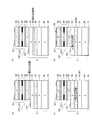
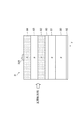
- (A) is sectional drawing of the thyristor which concerns on 1st Embodiment provided with a voltage reduction layer
- (b) is sectional drawing of a thyristor which is not provided with a voltage reduction layer
- (c) is thyristor characteristic. It is a figure explaining the band gap energy of the material which comprises a semiconductor layer. It is a figure which further demonstrates the laminated structure of a setting thyristor and a light emitting diode.
- (A) is a schematic energy band diagram in the laminated structure of the setting thyristor and the light emitting diode
- (b) is an energy band diagram in the reverse bias state of the tunnel junction layer
- (c) is a current voltage of the tunnel junction layer. Show properties.
- FIG. 6 is a timing chart illustrating operations of the light emitting device and the light emitting chip. It is a figure explaining the manufacturing method of a light emitting chip.
- (A) is a semiconductor laminated body formation process
- (b) is an n-ohmic electrode and light exit opening protective layer formation process
- (c) is a tunnel junction layer extraction etching process
- (d) is a current in a current confinement layer.
- the blocking portion forming step, (e) is a p gate layer extraction etching step, and (f) is a p ohmic electrode and back electrode forming step. It is an expanded sectional view of the modification of the island by which the setting thyristor and the light emitting diode were laminated
- (A) shows a case where the voltage reduction layer is provided between the p gate layer and the n cathode layer of the setting thyristor
- (b) shows a case where the voltage reduction layer is provided between the n gate layer and the p gate layer of the setting thyristor.
- (c) shows a case where the voltage reduction layer is a p-gate layer
- (d) shows a case where the voltage reduction layer is an n-gate layer.
- FIG. It is an expanded sectional view of the optical thyristor which concerns on 5th Embodiment.
- FIG. 1 is a diagram illustrating an example of an overall configuration of an image forming apparatus 1 to which the first exemplary embodiment is applied.
- An image forming apparatus 1 shown in FIG. 1 is an image forming apparatus generally called a tandem type.
- the image forming apparatus 1 includes an image forming process unit 10 that forms an image corresponding to image data of each color, an image output control unit 30 that controls the image forming process unit 10, such as a personal computer (PC) 2 or an image reading device. 3 and an image processing unit 40 that performs predetermined image processing on image data received from these.
- PC personal computer
- the image forming process unit 10 includes image forming units 11Y, 11M, 11C, and 11K that are arranged in parallel at predetermined intervals (in the case where they are not distinguished, they are referred to as image forming units 11).
- the image forming unit 11 is an example of an image carrier that forms an electrostatic latent image and holds a toner image, and an example of a charging unit that charges the surface of the photoconductor drum 12 with a predetermined potential.
- a developing unit 15 as an example of a developing unit that develops an electrostatic latent image obtained by the print head 14.
- Each of the image forming units 11Y, 11M, 11C, and 11K forms toner images of yellow (Y), magenta (M), cyan (C), and black (K).
- the image forming process unit 10 performs multiple transfer of the toner images of each color formed on the photosensitive drums 12 of the image forming units 11Y, 11M, 11C, and 11K onto a recording sheet 25 as an example of a transfer target.
- a sheet conveying belt 21 that conveys the recording sheet 25
- a drive roll 22 that drives the sheet conveying belt 21,
- a transfer roll 23 that is an example of a transfer unit that transfers the toner image on the photosensitive drum 12 to the recording sheet 25.
- a fixing device 24 for fixing the toner image on the recording paper 25.
- the image forming process unit 10 performs an image forming operation based on various control signals supplied from the image output control unit 30.
- the image data received from the personal computer (PC) 2 or the image reading device 3 under the control of the image output control unit 30 is subjected to image processing by the image processing unit 40 and supplied to the image forming unit 11.
- the image processing unit 40 For example, in the black (K) image forming unit 11K, the photosensitive drum 12 is charged in a predetermined potential by the charger 13 while rotating in the direction of arrow A, and the image supplied from the image processing unit 40 is supplied. Exposure is performed by the print head 14 that emits light based on the data. As a result, an electrostatic latent image related to a black (K) color image is formed on the photosensitive drum 12.
- the electrostatic latent image formed on the photosensitive drum 12 is developed by the developing device 15, and a black (K) toner image is formed on the photosensitive drum 12.
- K black
- image forming units 11Y, 11M, and 11C yellow (Y), magenta (M), and cyan (C) color toner images are formed, respectively.
- Each color toner image on the photosensitive drum 12 formed by each image forming unit 11 is applied to the transfer roll 23 on the recording paper 25 supplied with the movement of the paper conveying belt 21 moving in the direction of arrow B. Electrostatic transfer is sequentially performed by the transfer electric field, and a composite toner image in which toner of each color is superimposed on the recording paper 25 is formed. Thereafter, the recording paper 25 on which the composite toner image has been electrostatically transferred is conveyed to the fixing device 24. The synthesized toner image on the recording paper 25 conveyed to the fixing device 24 is fixed on the recording paper 25 by the fixing device 24 by heat and pressure and discharged from the image forming apparatus 1.
- FIG. 2 is a cross-sectional view showing an example of the configuration of the print head 14.
- the print head 14 as an example of the exposure unit includes a light source unit 63 including a housing 61 and a plurality of light emitting elements that expose the photosensitive drum 12 (light emitting diodes LED as an example of the light emitting elements in the first embodiment).
- a light emitting device 65 as an example of the light emitting unit provided, and a rod lens array 64 as an example of an optical unit that forms an image of light emitted from the light source unit 63 on the surface of the photosensitive drum 12 are provided.
- the light emitting device 65 includes a circuit board 62 on which the above-described light source unit 63, a signal generation circuit 110 that drives the light source unit 63 (see FIG. 3 described later), and the like are mounted.
- the housing 61 is made of, for example, metal, supports the circuit board 62 and the rod lens array 64, and is set so that the light emitting surface of the light emitting element of the light source unit 63 becomes the focal plane of the rod lens array 64. Further, the rod lens array 64 is disposed along the axial direction of the photosensitive drum 12 (the main scanning direction, which is the X direction in FIGS. 3 and 4B described later).
- FIG. 3 is a top view of an example of the light emitting device 65.
- the light source unit 63 has light-emitting chips C1 to C40 as examples of 40 light-emitting components on the circuit board 62 (in the case of not distinguishing, the light-emitting device 65 is expressed as the light-emitting chip C).
- the light-emitting device 65 is expressed as the light-emitting chip C.
- the configurations of the light emitting chips C1 to C40 may be the same.
- “to” indicates a plurality of constituent elements each distinguished by a number, and includes those described before and after “to” and those between them.
- the light emitting chips C1 to C40 include the light emitting chip C1 to the light emitting chip C40 in numerical order.
- the light emitting device 65 includes a signal generation circuit 110 that drives the light source unit 63.
- the signal generation circuit 110 is configured by, for example, an integrated circuit (IC). Note that the light emitting device 65 does not have to include the signal generation circuit 110. At this time, the signal generation circuit 110 is provided outside the light emitting device 65 and supplies a control signal and the like for controlling the light emitting chip C via a cable or the like.
- the light emitting device 65 will be described as including the signal generation circuit 110. Details of the arrangement of the light emitting chips C will be described later.
- FIG. 4 is a diagram showing an example of the configuration of the light-emitting chip C, the configuration of the signal generation circuit 110 of the light-emitting device 65, and the configuration of wiring (lines) on the circuit board 62.
- 4A shows the configuration of the light-emitting chip C
- FIG. 4B shows the configuration of the signal generation circuit 110 of the light-emitting device 65 and the configuration of wiring (lines) on the circuit board 62.
- FIG. 4B shows the light emitting chips C1 to C9 among the light emitting chips C1 to C40.
- the light-emitting chip C includes a plurality of light-emitting elements (in the first embodiment, light-emitting diodes) arranged in a row along the long side on the surface of the substrate 80 having a rectangular surface shape on the side close to one side of the long side.
- a light emitting unit 102 including LEDs 1 to 128 (represented as a light emitting diode LED when not distinguished) is provided.
- the light emitting chip C has terminals ( ⁇ 1 terminal, ⁇ 2 terminal, Vga terminal, ⁇ I terminal) which are a plurality of bonding pads for taking in various control signals and the like at both ends in the long side direction of the surface of the substrate 80.
- These terminals are provided in order of the ⁇ I terminal and the ⁇ 1 terminal from one end of the substrate 80, and are provided in the order of the Vga terminal and the ⁇ 2 terminal from the other end of the substrate 80.
- the light emitting unit 102 is provided between the ⁇ 1 terminal and the ⁇ 2 terminal.
- a back electrode 92 (see FIG. 6 described later) is provided on the back surface of the substrate 80 as a Vsub terminal.
- the “row shape” is not limited to the case where a plurality of light emitting elements are arranged in a straight line as illustrated in FIG. 4A, and the light emitting elements of the plurality of light emitting elements are arranged in the column direction. It may be in a state where they are arranged with different shift amounts with respect to the direction orthogonal to the direction. For example, when a light emitting surface of a light emitting element (a region 311 of a light emitting diode LED in FIG. 6 described later) is a pixel, each light emitting element is displaced by several pixels or several tens of pixels in a direction orthogonal to the column direction. May be arranged. Moreover, you may arrange
- the configuration of the signal generation circuit 110 of the light emitting device 65 and the configuration of the wiring (lines) on the circuit board 62 will be described with reference to FIG.
- the signal generating circuit 110 and the light emitting chips C1 to C40 are mounted on the circuit board 62 of the light emitting device 65, and wirings (lines) for connecting the signal generating circuit 110 and the light emitting chips C1 to C40 are provided. ing.
- Image signal processed image data and various control signals are input to the signal generation circuit 110 from the image output control unit 30 and the image processing unit 40 (see FIG. 1).
- the signal generation circuit 110 performs rearrangement of image data, correction of light quantity, and the like based on these image data and various control signals.
- the signal generation circuit 110 includes a transfer signal generation unit 120 that transmits the first transfer signal ⁇ 1 and the second transfer signal ⁇ 2 to the light emitting chips C1 to C40 based on various control signals. Further, the signal generation circuit 110 transmits the lighting signals ⁇ I1 to ⁇ I40 (indicated as the lighting signal ⁇ I if not distinguished) to the light emitting chips C1 to C40 based on various control signals, respectively. 140.
- the signal generation circuit 110 supplies a reference potential supply unit 160 that supplies a reference potential Vsub that serves as a potential reference to the light emitting chips C1 to C40, and a power supply potential that supplies a power supply potential Vga for driving the light emitting chips C1 to C40.
- a supply unit 170 is provided.
- the odd-numbered light emitting chips C1, C3, C5,... are arranged in a line at intervals in the long side direction of each substrate 80.
- the even-numbered light emitting chips C2, C4, C6,... The odd-numbered light-emitting chips C1, C3, C5,... And the even-numbered light-emitting chips C2, C4, C6,. They are arranged in a zigzag pattern in a state rotated by 180 °.
- the positions of the light emitting chips C are also set so that the light emitting elements are arranged at predetermined intervals in the main scanning direction (X direction).
- the light emitting chips C1 to C40 of FIG. 4B are arranged with the light emitting elements of the light emitting unit 102 shown in FIG. 4A (in order of the numbers of the light emitting diodes LED1 to LED128 in the first embodiment). The direction of is indicated by an arrow.
- the circuit board 62 is provided with a power supply line 200a that is connected to a back electrode 92 (see FIG. 6 described later) serving as a Vsub terminal provided on the back surface of the substrate 80 of the light emitting chip C and supplies a reference potential Vsub. .
- the circuit board 62 is provided with a power supply line 200b that is connected to a Vga terminal provided on the light emitting chip C and supplies a power supply potential Vga for driving.
- the circuit board 62 includes a first transfer signal line 201 for transmitting the first transfer signal ⁇ 1 from the transfer signal generator 120 of the signal generation circuit 110 to the ⁇ 1 terminals of the light emitting chips C1 to C40, and the light emitting chips C1 to C40.
- a second transfer signal line 202 for transmitting the second transfer signal ⁇ 2 to the ⁇ 2 terminal is provided.
- the first transfer signal ⁇ 1 and the second transfer signal ⁇ 2 are transmitted in common (in parallel) to the light emitting chips C1 to C40.
- the lighting signals ⁇ I1 to ⁇ I40 are transmitted to the circuit board 62 from the lighting signal generator 140 of the signal generating circuit 110 to the respective ⁇ I terminals of the light emitting chips C1 to C40 via the current limiting resistors RI.
- Lighting signal lines 204-1 to 204-40 are provided.
- the reference potential Vsub and the power supply potential Vga are commonly supplied to all the light emitting chips C1 to C40 on the circuit board 62.
- the first transfer signal ⁇ 1 and the second transfer signal ⁇ 2 are also transmitted in common (in parallel) to the light emitting chips C1 to C40.
- the lighting signals ⁇ I1 to ⁇ I40 are individually transmitted to the light emitting chips C1 to C40, respectively.
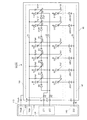
- FIG. 5 is an equivalent circuit diagram illustrating a circuit configuration of a light-emitting chip C on which a self-scanning light-emitting element array (SLED) according to the first embodiment is mounted.
- SLED self-scanning light-emitting element array
- Each element described below is arranged based on a layout (see FIG. 6 described later) on the light emitting chip C except for terminals ( ⁇ 1 terminal, ⁇ 2 terminal, Vga terminal, ⁇ I terminal). Note that the positions of the terminals ( ⁇ 1 terminal, ⁇ 2 terminal, Vga terminal, ⁇ I terminal) are different from those in FIG. 4A. Yes.
- the Vsub terminal provided on the back surface of the substrate 80 is drawn out of the substrate 80.
- the light emitting chip C will be described taking the light emitting chip C1 as an example in relation to the signal generation circuit 110. Therefore, in FIG. 5, the light-emitting chip C is referred to as a light-emitting chip C ⁇ b> 1 (C).
- the configuration of the other light emitting chips C2 to C40 is the same as that of the light emitting chip C1.
- the light-emitting chip C1 (C) includes a light-emitting unit 102 (see FIG. 4A) that includes light-emitting diodes LED1 to LED128.
- the light-emitting chip C1 (C) includes setting thyristors S1 to S128 (in the case where they are not distinguished, they are expressed as setting thyristors S).
- the light emitting diodes LED1 to LED128 and the setting thyristors S1 to S128, the light emitting diode LED and the setting thyristor S having the same number are connected in series.
- the light emitting diodes LED are stacked on the setting thyristors S arranged in a line on the substrate 80. Therefore, the light emitting diodes LED1 to LED128 are also arranged in a row.
- the light-emitting chip C1 (C) includes transfer thyristors T1 to T128 arranged in a row like the light-emitting diodes LED1 to LED128 and the setting thyristors S1 to S128 (in the case where they are not distinguished, they are referred to as transfer thyristors T).
- transfer thyristor T is used as an example of the transfer element, but other circuit elements may be used as long as the elements are sequentially turned on. For example, a circuit including a shift register and a plurality of transistors is combined. An element may be used.
- the light-emitting chip C1 (C) includes two pairs of transfer thyristors T1 to T128 in the order of numbers, and is represented by coupling diodes D1 to D127 (if not distinguished from each other), the coupling diode D. ). Further, the light emitting chip C1 (C) includes power supply line resistances Rg1 to Rg128 (in the case of not distinguishing, it is expressed as a power supply line resistance Rg).
- the light emitting chip C1 (C) includes one start diode SD.
- the transfer unit 101 includes the setting thyristors S1 to S128, the transfer thyristors T1 to T128, the power supply line resistors Rg1 to Rg128, the coupling diodes D1 to D127, the start diode SD, and the current limiting resistors R1 and R2.
- the light emitting diodes LED1 to LED128 of the light emitting unit 102, the transfer unit 101 and the setting thyristors S1 to S128, and the transfer thyristors T1 to T128 are arranged in numerical order from the left side in FIG. Further, the coupling diodes D1 to D127 and the power supply line resistors Rg1 to Rg128 are also arranged in numerical order from the left side in the figure. In FIG. 5, the transfer unit 101 and the light emitting unit 102 are arranged in this order from the top.
- the number of light emitting diodes LED in the light emitting unit 102, the setting thyristor S, the transfer thyristor T, and the power supply line resistance Rg in the transfer unit 101 are 128.
- the number of coupling diodes D is 127, which is one less than the number of transfer thyristors T.
- the number of light emitting diodes LED is not limited to the above, and may be a predetermined number.
- the number of transfer thyristors T may be larger than the number of light emitting diodes LED.
- the light emitting diode LED includes a two-terminal semiconductor element having an anode terminal (anode) and a cathode terminal (cathode), a thyristor (setting thyristor S, transfer thyristor T), an anode terminal (anode), a gate terminal (gate), and
- the semiconductor element having three terminals of the cathode terminal (cathode), the coupling diode D1, and the start diode SD are two-terminal semiconductor elements having an anode terminal (anode) and a cathode terminal (cathode).
- the light-emitting diode LED, thyristor (setting thyristor S, transfer thyristor T), coupling diode D1, and start diode SD may not necessarily include an anode terminal, a gate terminal, and a cathode terminal configured as electrodes. is there. Therefore, hereinafter, the terminal may be abbreviated and indicated in parentheses.
- the anodes of the transfer thyristor T and the setting thyristor S are connected to the substrate 80 of the light emitting chip C1 (C) (anode common). These anodes are connected to the power supply line 200a (see FIG. 4B) via a back electrode 92 (see FIG. 6B described later) which is a Vsub terminal provided on the back surface of the substrate 80. Is done.
- the power supply line 200a is supplied with the reference potential Vsub from the reference potential supply unit 160.
- This connection is a configuration when a p-type substrate 80 is used, and when an n-type substrate is used, the polarity is reversed, and an intrinsic (i) type (semi-insulating or insulating) to which no impurity is added.
- a terminal connected to the reference potential Vsub is provided on the side of the substrate where the transfer unit 101 and the light emitting unit 102 are provided.
- the cathodes of the odd-numbered transfer thyristors T1, T3,... are connected to the first transfer signal line 72.
- the first transfer signal line 72 is connected to the ⁇ 1 terminal via the current limiting resistor R1.
- the first transfer signal line 201 (see FIG. 4B) is connected to the ⁇ 1 terminal, and the first transfer signal ⁇ 1 is transmitted from the transfer signal generator 120.
- the cathodes of the even-numbered transfer thyristors T2, T4,... are connected to the second transfer signal line 73 along the arrangement of the transfer thyristors T.
- the second transfer signal line 73 is connected to the ⁇ 2 terminal via the current limiting resistor R2.
- the second transfer signal line 202 (see FIG. 4B) is connected to the ⁇ 2 terminal, and the second transfer signal ⁇ 2 is transmitted from the transfer signal generator 120.
- the cathodes of the light emitting diodes LED1 to LED128 are connected to the lighting signal line 75.
- the lighting signal line 75 is connected to the ⁇ I terminal.
- the ⁇ I terminal is connected to the lighting signal line 204-1 via the current limiting resistor RI provided outside the light emitting chip C1 (C), and the lighting signal generating unit 140 transmits the lighting signal ⁇ I1. (See FIG. 4B).
- the lighting signal ⁇ I1 supplies a current for lighting to the light emitting diodes LED1 to LED128.
- the lighting signal lines 204-2 to 204-40 are connected to the ⁇ I terminals of the other light emitting chips C2 to C40 via current limiting resistors RI, respectively, and the lighting signals ⁇ I2 to ⁇ I40 are transmitted from the lighting signal generator 140. (See FIG. 4B).
- the gates Gt1 to Gt128 of the transfer thyristors T1 to T128 are represented by the gates Gs1 to Gs128 of the setting diodes S1 to S128 having the same number (represented as the gate Gs if not distinguished). To 1). Therefore, the gates Gt1 to Gt128 and the gates Gs1 to Gs128 have the same number and are electrically at the same potential. Therefore, for example, it is expressed as a gate Gt1 (gate Gs1) and indicates that the potentials are the same.
- Coupling diodes D1 to D127 are connected between the gates Gt of the transfer thyristors T1 to T128, each paired with two gates Gt1 to Gt128 in order of number. That is, the coupling diodes D1 to D127 are connected in series so as to be sandwiched between the gates Gt1 to Gt128, respectively.
- the direction of the coupling diode D1 is connected in a direction in which current flows from the gate Gt1 to the gate Gt2. The same applies to the other coupling diodes D2 to D127.
- the gate Gt (gate Gs) of the transfer thyristor T is connected to the power supply line 71 via the power supply line resistance Rg provided corresponding to each of the transfer thyristors T.
- the power supply line 71 is connected to the Vga terminal.
- a power supply line 200b (see FIG. 4B) is connected to the Vga terminal, and the power supply potential Vga is supplied from the power supply potential supply unit 170.
- the gate Gt1 of the transfer thyristor T1 is connected to the cathode terminal of the start diode SD.
- the anode of the start diode SD is connected to the second transfer signal line 73.
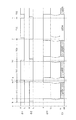
- FIG. 6 is an example of a plan layout view and a cross-sectional view of the light emitting chip C according to the first embodiment.
- 6A is a plan layout view of the light-emitting chip C
- FIG. 6B is a cross-sectional view taken along the line VIB-VIB of FIG. 6A.
- FIG. 6A shows a portion centering on the light emitting diodes LED1 to LED4, the setting thyristors S1 to S4, and the transfer thyristors T1 to T4.
- a Vsub terminal (back surface electrode 92) provided on the back surface of the substrate 80 is drawn out of the substrate 80. If the terminals are provided corresponding to (a) of FIG. 4, the ⁇ 2 terminal, the ⁇ I terminal, and the current limiting resistor R2 are provided at the right end portion of the substrate 80.
- the start diode SD may be provided at the right end portion of the substrate 80.
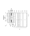
- FIG. 6B which is a cross-sectional view taken along the line VIB-VIB in FIG. 6A, the light emitting diode LED1 / setting thyristor S1, the transfer thyristor T1, the coupling diode D1, and the power supply line resistance Rg1 are shown from the bottom in the figure. It is shown. The light emitting diode LED1 and the setting thyristor S1 are stacked.
- main elements and terminals are represented by names.
- a p-type substrate 80 substrate 80
- a p-type anode layer 81 p anode layer 81
- a voltage reduction layer 90 an n-type gate layer 82 (n-gate layer 82), a p-type gate layer 83 ( A p-gate layer 83) and an n-type cathode layer 84 (n-cathode layer 84) are provided in this order.
- the notation in () is used. The same applies to other cases.
- a tunnel junction (tunnel diode) layer 85 is provided on the n cathode layer 84.
- a p-type anode layer 86 (p anode layer 86), a light emitting layer 87, and an n-type cathode layer 88 (n cathode layer 88) are provided on the tunnel junction layer 85.
- a light emitting port protective layer 89 made of an insulating material that transmits light emitted from the light emitting diode LED is provided.
- the voltage reduction layer 90 may be a p-type having the same impurity concentration as the p-anode layer 81 and a p-anode layer together with the p-anode layer 81.
- the voltage reduction layer 90 may be an n-type having an impurity concentration similar to that of the n-gate layer 82 and may be an n-gate layer together with the n-gate layer 82.
- the p anode layer 81 is an example of the first semiconductor layer
- the n gate layer 82 is an example of the second semiconductor layer
- the p gate layer 83 is an example of the third semiconductor layer
- the n cathode layer 84 is the fourth semiconductor layer. It is an example of a semiconductor layer.
- the voltage reduction layer 90 is included in the p anode layer, the voltage reduction layer 90 is included in the first semiconductor layer.
- the voltage reduction layer 90 is included in the n gate layer, the voltage reduction layer 90 is included in the second semiconductor layer.
- the voltage reduction layer 90 may be an i layer.
- the light emitting chip C is provided with a protective layer 91 made of a translucent insulating material provided so as to cover the surface and side surfaces of these islands. Yes.
- These islands and wiring such as the power supply line 71, the first transfer signal line 72, the second transfer signal line 73, the lighting signal line 75, and the like are through holes provided in the protective layer 91 ((a) in FIG. 6). (Indicated by ⁇ ) In the following description, description of the protective layer 91 and the through hole is omitted.
- a back surface electrode 92 serving as a Vsub terminal is provided on the back surface of the substrate 80.
- the p anode layer 81, the voltage reduction layer 90, the n gate layer 82, the p gate layer 83, the n cathode layer 84, the tunnel junction layer 85, the p anode layer 86, the light emitting layer 87, and the n cathode layer 88 are each a semiconductor layer. Then, the layers are sequentially stacked by epitaxial growth. Then, the semiconductor layer between the islands is removed by etching (mesa etching) so as to become a plurality of islands (islands) separated from each other (islands 301, 302, 303,... Described later).
- the p anode layer 81 may or may not be separated. In FIG. 6B, the p anode layer 81 is partially separated in the thickness direction. The p anode layer 81 may also serve as the substrate 80.
- a setting thyristor S Using the p anode layer 81, the voltage reduction layer 90, the n gate layer 82, the p gate layer 83, and the n cathode layer 84, a setting thyristor S, a transfer thyristor T, a coupling diode D, a power supply line resistance Rg, and the like (( In b), a setting thyristor S1, a transfer thyristor T1, a coupling diode D1, and a power supply line resistance Rg1) are configured.
- the notations of the p anode layer 81, the voltage reduction layer 90, the n gate layer 82, the p gate layer 83, and the n cathode layer 84 correspond to functions (functions) when the setting thyristor S and the transfer thyristor T are configured. ing. That is, the p anode layer 81 functions as an anode, the n gate layer 82 and the p gate layer 83 function as a gate, and the n cathode layer 84 functions as a cathode.
- the voltage reduction layer 90 functions as a part of the p anode layer 81 or a part of the n gate layer 82 as described later. In the case of configuring the coupling diode D and the power supply line resistance Rg, different functions (functions) are performed as described later.
- the p anode layer 86, the light emitting layer 87, and the n cathode layer 88 constitute a light emitting diode LED (light emitting diode LED1 in FIG. 6B).
- the notation of the p anode layer 86 and the n cathode layer 88 is the same, and corresponds to the function (function) when the light emitting diode LED is configured. That is, the p anode layer 86 functions as an anode, and the n cathode layer 88 functions as a cathode.
- the plurality of islands include a p anode layer 81, a voltage reduction layer 90, an n gate layer 82, a p gate layer 83, an n cathode layer 84, a part or all of the tunnel junction layer 85, a p anode layer. 86, the light emitting layer 87, and the n cathode layer 88, which do not include some of the layers.
- the island 302 does not include the tunnel junction layer 85, the p anode layer 86, the light emitting layer 87, and the n cathode layer 88.
- the plurality of islands include those that do not include part of the layer.
- the island 302 includes a p anode layer 81, a voltage reduction layer 90, an n gate layer 82, a p gate layer 83, and an n cathode layer 84, but the n cathode layer 84 includes only a part.
- the island 301 is provided with a setting thyristor S1 and a light emitting diode LED1.
- a transfer thyristor T1 and a coupling diode D1 are provided in the island 302, a transfer thyristor T1 and a coupling diode D1 are provided in the island 302, a transfer thyristor T1 and a coupling diode D1 are provided in the island 302, a transfer thyristor T1 and a coupling diode D1 are provided.
- the island 303 is provided with a power supply line resistance Rg1.
- the island 304 is provided with a start diode SD.
- the island 305 is provided with a current limiting resistor R1
- the island 306 is provided with a current limiting resistor R2.
- a plurality of islands similar to the islands 301, 302, and 303 are formed in parallel. These islands include setting thyristors S2, S3, S4,..., Light emitting diodes
- the island 301 is provided with a setting thyristor S1 and a light emitting diode LED1.
- the setting thyristor S1 includes a p anode layer 81, a voltage reduction layer 90, an n gate layer 82, a p gate layer 83, and an n cathode layer 84.
- a p-type ohmic electrode 331 (p-ohmic electrode) provided on the p-gate layer 83 exposed by removing the n-cathode layer 88, the light-emitting layer 87, the p-anode layer 86, the tunnel junction layer 85, and the n-cathode layer 84 is removed.
- the electrode 331) is an electrode of the gate Gs1 (may be referred to as a gate terminal Gs1).
- the light emitting diode LED1 is composed of a p anode layer 86, a light emitting layer 87, and an n cathode layer 88.
- the light emitting diode LED1 is stacked via the tunnel junction layer 85 on the n cathode layer 84 of the setting thyristor S1.
- An n-type ohmic electrode 321 (n-ohmic electrode 321) provided on the n-cathode layer 88 (region 311) is used as a cathode electrode.
- the p anode layer 86 includes a current confinement layer 86b (see FIG. 7 described later).
- the current confinement layer 86b is provided to limit the current flowing through the light emitting diode LED to the central portion of the light emitting diode LED. That is, the periphery of the light emitting diode LED has many defects due to mesa etching. For this reason, non-radiative recombination tends to occur. Therefore, the current confinement layer 86b is provided so that the central portion of the light emitting diode LED becomes the current passage portion ⁇ where current flows easily and the peripheral portion becomes the current blocking portion ⁇ where current does not flow easily. As shown in the light emitting diode LED1 in FIG. 6A, the inner side of the broken line is the current passage part ⁇ , and the outer side of the broken line is the current blocking part ⁇ .
- the n-ohmic electrode 321 is provided in the peripheral portion of the light emitting diode LED1 so that the central portion is an opening.
- the current confinement layer 86b will be described later.
- the current confinement layer 86b When the current confinement layer 86b is provided, power consumed for non-radiative recombination is suppressed, so that power consumption is reduced and light extraction efficiency is improved.
- the light extraction efficiency is the amount of light that can be extracted per electric power.
- the transfer thyristor T1 includes a p anode layer 81, a voltage reduction layer 90, an n gate layer 82, a p gate layer 83, and an n cathode layer 84. That is, the n ohmic electrode 323 provided on the n cathode layer 84 (region 313) exposed by removing the n cathode layer 88, the light emitting layer 87, the p anode layer 86, and the tunnel junction layer 85 is used as a cathode terminal.
- the n ++ layer 85a of the tunnel junction layer 85 may be an n-ohmic electrode 323 provided on the n ++ layer 85a of the tunnel junction layer 85.
- the p ohmic electrode 332 provided on the p gate layer 83 exposed by removing the n cathode layer 84 is used as a terminal of the gate Gt1 (may be referred to as a gate terminal Gt1).
- the coupling diode D ⁇ b> 1 provided on the island 302 includes a p gate layer 83 and an n cathode layer 84.
- the n ohmic electrode 324 provided on the n cathode layer 84 (region 314) exposed by removing the n cathode layer 88, the light emitting layer 87, the p anode layer 86, and the tunnel junction layer 85 is used as a cathode terminal.
- the n ++ layer 85a of the tunnel junction layer 85 may not be removed, and the n ohmic electrode 324 may be provided on the n ++ layer 85a of the tunnel junction layer 85.
- the p ohmic electrode 332 provided on the p gate layer 83 exposed by removing the n cathode layer 84 is used as an anode terminal.
- the anode terminal of the coupling diode D1 is the same as the gate Gt1 (gate terminal Gt1).
- the power supply line resistance Rg1 provided on the island 303 is composed of a p-gate layer 83.
- the p ohmic electrode 333 and the p ohmic electrode provided on the p gate layer 83 exposed by removing the n cathode layer 88, the light emitting layer 87, the p anode layer 86, the tunnel junction layer 85, and the n cathode layer 84.
- a p-gate layer 83 between the gate and the gate 334 is provided as a resistor.
- the start diode SD provided on the island 304 includes a p gate layer 83 and an n cathode layer 84. That is, the n ohmic electrode 325 provided on the n cathode layer 84 (region 315) exposed by removing the n cathode layer 88, the light emitting layer 87, the p anode layer 86, and the tunnel junction layer 85 is used as a cathode terminal. Note that the n ohm electrode 325 may be provided on the n ++ layer 85a of the tunnel junction layer 85 without removing the n ++ layer 85a of the tunnel junction layer 85.
- the p ohmic electrode 335 provided on the p gate layer 83 exposed by removing the n cathode layer 84 is used as an anode terminal.
- the current limiting resistor R1 provided on the island 305 and the current limiting resistor R2 provided on the island 306 are provided in the same manner as the power supply line resistor Rg1 provided on the island 303.
- the p gate layer 83 in between is used as a resistance.
- the lighting signal line 75 includes a trunk portion 75a and a plurality of branch portions 75b.
- the trunk portion 75a is provided so as to extend in the column direction of the light emitting diodes LED.
- the branch portion 75 b branches off from the trunk portion 75 a and is connected to an n ohmic electrode 321 that is a cathode terminal of the light emitting diode LED 1 provided on the island 301. The same applies to the cathode terminals of the other light emitting diodes LED.
- the lighting signal line 75 is connected to a ⁇ I terminal provided on the light emitting diode LED1 side.
- the first transfer signal line 72 is connected to an n-ohmic electrode 323 that is a cathode terminal of a transfer thyristor T1 provided on the island 302.
- the first transfer signal line 72 is connected to the cathode terminal of another odd-numbered transfer thyristor T provided on an island similar to the island 302.
- the first transfer signal line 72 is connected to the ⁇ 1 terminal via a current limiting resistor R1 provided on the island 305.
- the second transfer signal line 73 is connected to an n-ohmic electrode (unsigned) that is a cathode terminal of an even-numbered transfer thyristor T provided on an island without a symbol.
- the second transfer signal line 73 is connected to the ⁇ 2 terminal via a current limiting resistor R2 provided on the island 306.
- the power supply line 71 is connected to the p ohmic electrode 334 which is one terminal of the power supply line resistance Rg1 provided on the island 303. One terminal of the other power supply line resistor Rg is also connected to the power supply line 71.
- the power supply line 71 is connected to the Vga terminal.
- the p ohmic electrode 331 (gate terminal Gs1) of the light emitting diode LED1 provided on the island 301 is connected to the p ohmic electrode 332 (gate terminal Gt1) of the island 302 by a connection wiring 76.
- the p ohmic electrode 332 (gate terminal Gt1) is connected to the p ohmic electrode 333 (the other terminal of the power supply line resistance Rg1) of the island 303 by a connection wiring 77.
- An n-ohmic electrode 324 (cathode terminal of the coupling diode D1) provided on the island 302 is connected by a connection wiring 79 to a p-type ohmic electrode (not indicated) which is the gate terminal Gt2 of the adjacent transfer thyristor T2.
- the p ohmic electrode 332 (gate terminal Gt1) of the island 302 is connected to the n ohmic electrode 325 (cathode terminal of the start diode SD) provided on the island 304 by a connection wiring 78.
- the p ohmic electrode 335 (the anode terminal of the start diode SD) is connected to the second transfer signal line 73.
- the above connection / configuration is a configuration when a p-type substrate 80 is used, and the polarity is reversed when an n-type substrate is used.
- a terminal connected to the power supply line 200a for supplying the reference potential Vsub is provided on the side of the substrate where the transfer unit 101 and the light emitting unit 102 are provided. Connections and configurations are the same as in the case of using the p-type substrate 80 and the case of using the n-type substrate.
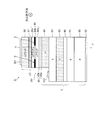
- FIG. 7 is an enlarged cross-sectional view of the island 301 in which the setting thyristor S and the light emitting diode LED are stacked. Note that the light exit opening protective layer 89 and the protective layer 91 are omitted. The same applies hereinafter. As described above, the light emitting diode LED is stacked on the setting thyristor S via the tunnel junction layer 85. That is, the setting thyristor S and the light emitting diode LED are connected in series.
- the setting thyristor S includes a p anode layer 81, a voltage reduction layer 90, an n gate layer 82, a p gate layer 83, and an n cathode layer 84. That is, the voltage reduction layer 90 is added to the four-layer structure of pnpn.
- the voltage reduction layer 90 may be p-type having the same impurity concentration as the p anode layer 81 as a part of the p anode layer 81, and the same impurity as the n gate layer 82 as a part of the n gate layer 82. It may be n-type in concentration.
- the voltage reduction layer 90 may be an i layer.
- the tunnel junction layer 85 includes an n ++ layer 85a in which an n-type impurity (dopant) is added (doped) at a high concentration, and a p ++ layer 85b in which a p-type impurity is added at a high concentration.
- the light emitting diode LED includes a p anode layer 86, a light emitting layer 87, and an n cathode layer 88.
- the light emitting layer 87 has a quantum well structure in which well layers and barrier layers are alternately stacked.
- the light emitting layer 87 may be an i layer.
- the light emitting layer may have a structure other than the quantum well structure, and may be, for example, a quantum beam (quantum wire) or a quantum box (quantum dot).
- the p anode layer 86 is composed of a laminated lower p layer 86a, current confinement layer 86b, and upper p layer 86c.
- the current confinement layer 86b includes a current passage portion ⁇ and a current blocking portion ⁇ . As shown in FIG. 6A, the current passage part ⁇ is provided in the central part of the light emitting diode LED, and the current blocking part ⁇ is provided in the peripheral part of the light emitting diode LED.
- FIG. 8 is a diagram for explaining the structure of the thyristor and the characteristics of the thyristor.
- 8A is a cross-sectional view of the thyristor according to the first embodiment including the voltage reduction layer 90
- FIG. 8B is a cross-sectional view of the thyristor not including the voltage reduction layer 90
- FIG. (C) is a thyristor characteristic.
- FIGS. 8A and 8B show cross sections of the transfer thyristor T in which the light emitting diodes LED are not stacked.
- the setting thyristor S in which the light emitting diodes LED are stacked also exhibits the same characteristics. As shown in FIG.
- the thyristor (transfer thyristor T, setting thyristor S) according to the first embodiment includes a voltage reduction layer 90 between a p anode layer 81 and an n gate layer 82.
- the voltage reduction layer 90 is a p-type having the same impurity concentration as the p-anode layer 81, it functions as a part of the p-anode layer 81, and if it is an n-type having the same impurity concentration as the n-gate layer 82, It works as a part of the n gate layer 82.
- the voltage reduction layer 90 may be an i layer.
- the thyristor shown in FIG. 8B does not include the voltage reduction layer 90.
- the rising voltage Vr in the thyristor is determined by the smallest band gap energy (band gap energy) in the semiconductor layer constituting the thyristor.
- the rising voltage Vr in the thyristor is a voltage when the current in the ON state of the thyristor is extrapolated to the voltage axis.
- the band gap energy is smaller than that of the p anode layer 81, the n gate layer 82, the p gate layer 83, and the n cathode layer 84.
- a voltage reduction layer 90 is provided.
- the rising voltage Vr of the thyristor according to the first embodiment is lower than the rising voltage Vr ′ of the thyristor that does not include the voltage reduction layer 90.
- the voltage reduction layer 90 is a layer having a band gap smaller than the band gap of the light emitting layer 87 as an example.
- the thyristor according to the first embodiment is not used as a light-emitting component, but functions as a part of a drive circuit that drives a light-emitting component such as a light-emitting diode LED. Therefore, the band gap is determined regardless of the emission wavelength of the light emitting component that actually emits light.
- the rising voltage Vr of the thyristor is reduced.
- the voltage applied to the thyristor and the light emitting element is also reduced in a state where the thyristor and the light emitting element are turned on.
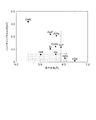
- FIG. 9 is a diagram for explaining the band gap energy of the material constituting the semiconductor layer.
- the lattice constant of GaAs is about 5.65 ⁇ .
- the lattice constant of AlAs is about 5.66 ⁇ . Therefore, a material close to this lattice constant can be epitaxially grown on the GaAs substrate.
- AlGaAs or Ge which is a compound of GaAs and AlAs, can be epitaxially grown on a GaAs substrate.
- the lattice constant of InP is about 5.875. A material close to this lattice constant can be epitaxially grown on the InP substrate.
- the lattice constant of GaN varies depending on the growth surface, but is 3.19 mm for the a-plane and 5.17 mm for the c-plane.
- a material close to this lattice constant can be epitaxially grown on the GaN substrate.
- the band gap energy at which the rising voltage of the thyristor becomes smaller than that of GaAs, InP, and GaN is a material in the range indicated by the halftone dots in FIG. That is, when a material in the range indicated by the halftone dots is used as a layer constituting the thyristor, the rising voltage Vr of the thyristor becomes the band gap energy of the material in the region indicated by the halftone dots.
- the band gap energy of GaAs is about 1.43 eV. Therefore, if the voltage reduction layer 90 is not used, the rising voltage Vr of the thyristor is about 1.43V.
- the rising voltage Vr of the thyristor can be more than 0 V and less than 1.43 V (0 V ⁇ Vr ⁇ 1.43 V). ). This reduces power consumption when the thyristor is in the on state.
- GaAs and InP substrate As a material in a range indicated by a halftone dot, there is Ge having a band gap energy of about 0.67 eV with respect to GaAs. Further, there is InAs having a band gap energy of about 0.36 eV with respect to InP.
- a material having a small band gap energy can be used for a GaAs and InP substrate, a compound of GaAs and InP, a compound of InN and InSb, a compound of InN and InAs, and the like.
- mixed compounds based on GaInNAs are suitable. These may include Al, Ga, As, P, Sb, and the like.
- GANP can be the voltage reduction layer 90.
- InN layer InGaN layer by metamorphic growth
- Quantum dots made of InN, InGaN, InNAs, InNSb
- An InAsSb layer or the like can be introduced as the voltage reduction layer 90.
- These may include Al, Ga, N, As, P, Sb, and the like.
- the rising voltages Vr and Vr ′ of the thyristor have been described, but the same applies to the holding voltages Vh and Vh ′ which are the minimum voltages for maintaining the thyristor in the on state and the voltage applied to the thyristor in the on state (FIG. 8 (c)).
- the switching voltage Vs of the thyristor is determined by the depletion layer of the semiconductor layer that is reverse biased. Therefore, the voltage reduction layer 90 has a small influence on the switching voltage Vs of the thyristor.
- the voltage reduction layer 90 reduces the rising voltage Vr while maintaining the switching voltage Vs of the thyristor. Thereby, the voltage applied to the thyristor in the on state is reduced, and the power consumption is reduced.
- the switching voltage Vs of the thyristor is set to an arbitrary value by adjusting the material, impurity concentration, and the like of the p anode layer 81, the n gate layer 82, the p gate layer 83, and the n cathode layer 84. However, the switching voltage Vs varies depending on the insertion position of the voltage reduction layer 90.
- FIG. 10 is a diagram for further explaining the laminated structure of the setting thyristor S and the light emitting diode LED.
- 10A is a schematic energy band diagram in the laminated structure of the setting thyristor S and the light emitting diode LED
- FIG. 10B is an energy band diagram in the reverse bias state of the tunnel junction layer 85
- FIG. (C) shows the current-voltage characteristics of the tunnel junction layer 85.
- a reverse bias is applied between the n ++ layer 85a and the p ++ layer 85b of the tunnel junction layer 85.
- the tunnel junction layer 85 (tunnel junction) is a junction between an n ++ layer 85a to which n-type impurities are added at a high concentration and a p ++ layer 85b to which p-type impurities are added at a high concentration. Therefore, when the width of the depletion region is narrow and forward biased, electrons tunnel from the conduction band (conduction band) on the n ++ layer 85a side to the valence band (valence band) on the p ++ layer 85b side. At this time, negative resistance characteristics appear. On the other hand, as shown in FIG.
- the setting thyristor S when the setting thyristor S is turned on, a current flows between the setting thyristor S and the light emitting diode LED even if the tunnel junction layer 85 is reverse-biased. Thereby, the light emitting diode LED emits light (lights up).
- the setting thyristor S is in a state where it can transition to the on state when the connected transfer thyristor T is turned on and turned on.
- the lighting signal ⁇ I becomes “L”
- the setting thyristor S is turned on and turned on, and the light emitting diode LED is turned on (lighting is set). Therefore, in this specification, it is expressed as “setting thyristor”.
- the thyristor is a semiconductor element having three terminals of an anode terminal (anode), a cathode terminal (cathode), and a gate terminal (gate).
- anode layer 81, p gate layer 83, an n-type semiconductor layer (n gate layer 82, n cathode layer 84), and a voltage reduction layer 90 containing Ge or Ge are stacked on the substrate 80.
- the voltage reduction layer 90 functions as p-type or n-type.
- the forward potential (diffusion potential) Vd of a pn junction composed of a p-type semiconductor layer and an n-type semiconductor layer is set to 1.5 V as an example.
- the voltage between the cathode and anode of the thyristor in the on state is 1 V, which is smaller than the forward potential Vd (1.5 V) of the pn junction by the voltage reduction layer 90. If the voltage reduction layer 90 is not provided, the voltage between the cathode and the anode of the thyristor in the on state is the forward potential Vd (1.5 V) of the pn junction. In the following description, by providing the voltage reduction layer 90, the voltage between the cathode and the anode of the thyristor in the on state is 0.5V smaller. Note that the voltage between the cathode and anode of the thyristor in the on state is determined by the voltage reduction layer 90 used.
- the reference potential Vsub supplied to the back electrode 92 (see FIGS. 5 and 6), which is the Vsub terminal, is supplied to the 0 V and Vga terminals as a high level potential (hereinafter referred to as “H”).
- the power supply potential Vga will be described as ⁇ 3.3 V as a low level potential (hereinafter referred to as “L”).
- the anode of the thyristor is a reference potential Vsub (“H” (0 V)) supplied to the back electrode 92.
- An off-state thyristor in which no current flows between the anode and the cathode is turned on (turned on) when a potential lower than the threshold voltage (a negative potential having a large absolute value) is applied to the cathode.
- the threshold voltage of the thyristor is a value obtained by subtracting the forward potential Vd (1.5 V) of the pn junction from the potential of the gate.
- the gate of the thyristor becomes a potential close to the potential of the anode terminal.
- the anode is set to the reference potential Vsub (“H” (0 V))
- the gate is assumed to be 0 V (“H”).
- the cathode of the thyristor in the on state becomes ⁇ 1V.
- An on-state thyristor is turned off when the cathode is at a higher potential (a negative potential with a small absolute value, 0 V or a positive potential) than the potential necessary to maintain the on-state (the potential close to the above -1V). Enter state (turn off).
- a potential lower than the potential necessary for maintaining the on state (a negative potential having a large absolute value) is continuously applied to the cathode of the on thyristor, and the current that can maintain the on state (sustain current). Is supplied, the thyristor remains on.
- the setting thyristor S is stacked with the light emitting diode LED and connected in series. Therefore, the voltage applied to the cathode (n cathode layer 84) of the setting thyristor S is a voltage obtained by dividing the potential of the lighting signal ⁇ I by the setting thyristor S and the light emitting diode LED.
- ⁇ 3.3 V is applied to the setting thyristor S when the setting thyristor S is in the OFF state.
- a lighting signal ⁇ I (“Lo”, which will be described later) applied when the light emitting diode LED is turned on is set to ⁇ 5V, for example.
- 1.7V is applied between the anode and cathode of light emitting diode LED.
- the voltage applied to the light emitting diode LED is -1.7V.
- the lighting signal ⁇ I (“Lo”) supplied to the ⁇ I terminal may be adjusted.
- the n gate layer 82 and the p gate layer 83 of the thyristor are made of a semiconductor such as GaAs, light may be emitted between the n gate layer 82 and the p gate layer 83 in the on state.
- the amount of light emitted from the thyristor is determined by the area of the cathode and the current flowing between the cathode and the anode. Therefore, when light emission from the thyristor is not used, for example, in the transfer thyristor T, unnecessary area of light can be reduced by reducing the area of the cathode or shielding light with an electrode (n-ohmic electrode 323 of the transfer thyristor T1). You may make it suppress.
- FIG. 11 is a timing chart for explaining operations of the light emitting device 65 and the light emitting chip C.
- FIG. 11 shows a timing chart of a portion that controls lighting (non-lighting) of the five light emitting diodes LED1 to LED5 of the light emitting chip C1.
- the light emitting diodes LED1, LED2, LED3, and LED5 of the light emitting chip C1 are turned on, and the light emitting diode LED4 is turned off (not lit).
- the light emitting diode LED1 is turned on or off in the period T (1)
- the light emitting diode LED2 is turned on in the period T (2)
- the light emitting diode LED3 is turned on in the period T (3)
- the light emitting diode LED4 is turned on or off in the period T (4).
- Lighting control (lighting control) is performed. Thereafter, lighting control of the light emitting diodes LED having a number of 5 or more is similarly performed.
- the periods T (1), T (2), T (3),... Have the same length, and are referred to as the period T when they are not distinguished from each other.
- the first transfer signal ⁇ 1 transmitted to the ⁇ 1 terminal (see FIGS. 5 and 6) and the second transfer signal ⁇ 2 transmitted to the ⁇ 2 terminal (see FIGS. 5 and 6) are “H” (0 V) and “L”. ”( ⁇ 3.3 V).
- the waveforms of the first transfer signal ⁇ 1 and the second transfer signal ⁇ 2 are repeated in units of two consecutive periods T (for example, the period T (1) and the period T (2)).
- “H” (0 V) and “L” ( ⁇ 3.3 V) may be abbreviated as “H” and “L”.
- the first transfer signal ⁇ 1 shifts from “H” (0V) to “L” ( ⁇ 3.3V) at the start time b of the period T (1), and shifts from “L” to “H” at the time f. . Then, at the end time i of the period T (2), the state shifts from “H” to “L”.
- the second transfer signal ⁇ 2 is “H” (0 V) at the start time b of the period T (1), and shifts from “H” (0 V) to “L” ( ⁇ 3.3 V) at the time e. Then, “L” is shifted to “H” at the end time i of the period T (2).
- the second transfer signal ⁇ 2 corresponds to the first transfer signal ⁇ 1 shifted after the period T on the time axis.
- the waveform indicated by the broken line and the waveform in the period T (2) are repeated after the period T (3).
- the waveform of the period T (1) of the second transfer signal ⁇ 2 is different from that after the period T (3) because the period T (1) is a period during which the light emitting device 65 starts operating.
- a set of transfer signals of the first transfer signal ⁇ 1 and the second transfer signal ⁇ 2 propagates the ON state of the transfer thyristor T in the order of numbers, thereby emitting light having the same number as the transfer thyristor T in the ON state.
- the diode LED is designated as a target for lighting or non-lighting control (lighting control).
- the lighting signal ⁇ I1 is a signal having two potentials of “H” (0 V) and “Lo” ( ⁇ 5 V).
- the lighting signal ⁇ I1 will be described in the lighting control period T (1) for the light emitting diode LED1 of the light emitting chip C1.
- the lighting signal ⁇ I1 is “H” (0V) at the start time b of the period T (1), and shifts from “H” (0V) to “L” ( ⁇ 3.3V) at the time c. Then, “L” is shifted to “H” at time d, and “H” is maintained at time e.
- the operations of the light emitting device 65 and the light emitting chip C1 will be described with reference to FIGS. 4 and 5 according to the timing chart shown in FIG. In the following, the periods T (1) and T (2) for controlling the lighting of the light emitting diodes LED1 and LED2 will be described.
- the reference potential supply unit 160 of the signal generation circuit 110 of the light emitting device 65 sets the reference potential Vsub to “H” (0 V).
- the power supply potential supply unit 170 sets the power supply potential Vga to “L” ( ⁇ 3.3 V).
- the power supply line 200a on the circuit board 62 of the light emitting device 65 becomes “H” (0 V) of the reference potential Vsub, and the Vsub terminals of the light emitting chips C1 to C40 become “H”.
- the power supply line 200b becomes “L” ( ⁇ 3.3 V) of the power supply potential Vga, and the Vga terminals of the light emitting chips C1 to C40 become “L” (see FIG. 4).
- the power supply line 71 of each of the light emitting chips C1 to C40 becomes “L” (see FIG. 5).
- the transfer signal generation unit 120 of the signal generation circuit 110 sets the first transfer signal ⁇ 1 and the second transfer signal ⁇ 2 to “H” (0 V), respectively.
- the first transfer signal line 201 and the second transfer signal line 202 become “H” (see FIG. 4).
- the ⁇ 1 terminal and ⁇ 2 terminal of each of the light emitting chips C1 to C40 become “H”.
- the potential of the first transfer signal line 72 connected to the ⁇ 1 terminal via the current limiting resistor R1 also becomes “H”
- the second transfer signal line 73 connected to the ⁇ 1 terminal via the current limiting resistor R2 is also set. It becomes “H” (see FIG. 5).
- the lighting signal generation unit 140 of the signal generation circuit 110 sets the lighting signals ⁇ I1 to ⁇ I40 to “H” (0 V), respectively. Then, the lighting signal lines 204-1 to 204-40 become “H” (see FIG. 4). Accordingly, the ⁇ I terminals of the light emitting chips C1 to C40 are set to “H” via the current limiting resistor RI, and the lighting signal line 75 connected to the ⁇ I terminal is also set to “H” (0 V) (FIG. 5). reference).
- the cathodes of the odd-numbered transfer thyristors T1, T3, T5,... Are connected to the first transfer signal line 72 and set to “H” (0 V).
- the cathodes of the even-numbered transfer thyristors T2, T4, T6,... Are connected to the second transfer signal line 73 and set to “H”. Therefore, the transfer thyristor T is in the off state because both the anode and the cathode are “H”.
- the cathode terminal of the light emitting diode LED is connected to the lighting signal line 75 of “H” (0 V). That is, the light emitting diode LED and the setting thyristor S are connected in series via the tunnel junction layer 85. Since the cathode of the light emitting diode LED is “H” and the anode of the setting thyristor S is “H”, the light emitting diode LED and the setting thyristor S are in the off state.
- the gate Gt1 is connected to the cathode of the start diode SD.
- the gate Gt1 is connected to the power supply line 71 of the power supply potential Vga (“L” ( ⁇ 3.3 V)) via the power supply line resistance Rg1.
- the anode terminal of the start diode SD is connected to the second transfer signal line 73, and is connected to the ⁇ 2 terminal of “H” (0 V) via the current limiting resistor R2. Therefore, the start diode SD is forward-biased, and the cathode (gate Gt1) of the start diode SD has the pn junction forward potential Vd (1.5 V) from the anode potential (“H” (0 V)) of the start diode SD. The value obtained by subtracting ( ⁇ 1.5V).
- the coupling diode D1 When the gate Gt1 becomes ⁇ 1.5V, the coupling diode D1 has an anode (gate Gt1) of ⁇ 1.5V and a cathode connected to the power supply line 71 (“L” ( ⁇ 3.3V) via the power supply line resistance Rg2. )), It is forward biased. Therefore, the potential of the gate Gt2 becomes ⁇ 3V obtained by subtracting the forward potential Vd (1.5V) of the pn junction from the potential of the gate Gt1 ( ⁇ 1.5V). However, the gates Gt numbered 3 or more are not affected by the fact that the anode of the start diode SD is “H” (0 V), and the potential of these gates Gt is “L” which is the potential of the power supply line 71. (-3.3V).
- the threshold voltage of the transfer thyristor T and the setting thyristor S is a value obtained by subtracting the forward potential Vd (1.5 V) of the pn junction from the potentials of the gates Gt and Gs. That is, the threshold voltage of the transfer thyristor T1 and the setting thyristor S1 is ⁇ 3 V, the threshold voltage of the transfer thyristor T2 and the setting thyristor S2 is ⁇ 4.5 V, the threshold voltage of the transfer thyristor T and the setting thyristor S having a number of 3 or more. Is -4.8V.
- the even-numbered transfer thyristor T cannot be turned on because the second transfer signal ⁇ 2 is “H” (0 V) and the second transfer signal line 73 is “H” (0 V).
- the transfer thyristor T1 is turned on, the potential of the first transfer signal line 72 becomes ⁇ 1 V from the potential of the anode (“H” (0 V)).
- the potential of the gate Gt1 / Gs1 becomes “H” (0 V) that is the potential of the anode of the transfer thyristor T1. Then, the potential of the gate Gt2 (gate Gs2) is ⁇ 1.5V, the potential of the gate Gt3 (gate Gs3) is ⁇ 3V, and the potential of the gate Gt (gate Gl) having a number of 4 or more is “L”.
- the threshold voltage of the setting thyristor S1 is -1.5V
- the threshold voltage of the transfer thyristor T2 is -3V
- the threshold voltage of the transfer thyristor T3 and the setting thyristor S3 is -4.5V
- the number is The threshold voltage of four or more transfer thyristors T and setting thyristors S becomes ⁇ 4.8V.
- the first transfer signal line 72 is set to ⁇ 1V by the on-state transfer thyristor T1
- the odd-numbered transfer thyristor T in the off state is not turned on.
- the second transfer signal line 73 is “H” (0 V)
- the even-numbered transfer thyristor T is not turned on.
- the lighting signal line 75 is “H” (0 V)
- none of the light emitting diodes LED is lit.
- the transfer thyristor T1 is in the on state, The transfer thyristor T, the setting thyristor S, and the light emitting diode LED are in the off state.
- the voltage between the anode and the cathode of the setting thyristor S1 becomes ⁇ 1V, so that the potential of the lighting signal line 75 becomes close to ⁇ 2.7V.
- the threshold voltage of the setting thyristor S2 is -3V, but the voltage applied to the setting thyristor S2 is -1V obtained by adding 1.7V to the voltage 1.7V applied to the light emitting diode LED. Thyristor S2 is not turned on. Immediately after time c, the transfer thyristor T1 and the setting thyristor S1 are in the on state, and the light emitting diode LED1 is lit (lights on).
- the lighting signal ⁇ I1 from the time c when the lighting signal ⁇ I1 shifts from “H” to “Lo” until the time d when the lighting signal ⁇ I1 shifts from “Lo” to “H” is “ Lo ”( ⁇ 5V).
- the transfer thyristor T1 is in the ON state.
- the second transfer signal ⁇ 2 shifts from “H” (0 V) to “L” ( ⁇ 3.3 V).
- the period T (1) for controlling the lighting of the light emitting diode LED1 ends, and the period T (2) for controlling the lighting of the light emitting diode LED2 starts.
- the second transfer signal ⁇ 2 shifts from “H” to “L”
- the potential of the second transfer signal line 73 shifts to ⁇ 1V via the ⁇ 2 terminal.
- the transfer thyristor T2 is turned on because the threshold voltage is -3V.
- the potential of the gate terminal Gt2 becomes “H” (0 V)
- the potential of the gate Gt3 becomes ⁇ 1.5 V
- the potential of the gate Gt4 becomes ⁇ 3 V.
- the potential of the gate Gt (gate Gs) having a number of 5 or more becomes ⁇ 3.3V.
- the transfer thyristors T1 and T2 are in the on state.
- the coupling diode D1 is in a state in which a potential is applied in a direction in which no current flows (reverse bias). Therefore, the influence of the gate Gt2 (gate Gs2) being “H” (0 V) does not reach the gate Gt1 (gate Gs1). That is, in the transfer thyristor T having the gate Gt connected by the reverse-biased coupling diode D, the threshold voltage becomes ⁇ 4.8V, and the first transfer signal ⁇ 1 or “L” ( ⁇ 3.3V) The 2 transfer signal ⁇ 2 does not turn on. Immediately after time f, the transfer thyristor T2 is in the ON state.
- the first transfer signal ⁇ 1 shifts from “H” (0 V) to “L” ( ⁇ 3.3 V) at time i, similarly to the transfer thyristor T1 at time b or the transfer thyristor T2 at time e.
- the transfer thyristor T3 having a threshold voltage of ⁇ 3V is turned on.
- the period T (2) for controlling the lighting of the light emitting diode LED2 ends, and the period T (3) for controlling the lighting of the light emitting diode LED3 starts. Thereafter, the above description is repeated.
- the lighting signal ⁇ I may remain “H” (0 V).
- the threshold voltage of the setting thyristor S4 is ⁇ 1.5 V, the setting thyristor S4 is not turned on, and the light emitting diode LED4 remains off (not lit).
- the gate terminals Gt of the transfer thyristors T are connected to each other by the coupling diode D. Therefore, when the potential of the gate Gt changes, the potential of the gate Gt connected to the gate Gt whose potential has changed via the forward-biased coupling diode D changes. Then, the threshold voltage of the transfer thyristor T having the gate whose potential has changed changes. In the transfer thyristor T, when the threshold voltage is higher than “L” ( ⁇ 3.3 V) (a negative value having a small absolute value), the first transfer signal ⁇ 1 or the second transfer signal ⁇ 2 is changed from “H” (0 V). Turns on at the timing of shifting to “L” ( ⁇ 3.3 V).
- the lighting signal ⁇ I changes from “H” (0 V) to “Lo” ( When the voltage shifts to ⁇ 5 V), the light emitting diode LED connected in series to the setting thyristor S is turned on (emits light).
- the transfer thyristor T is turned on to designate the light emitting diode LED that is the object of lighting control, and the lighting signal ⁇ I of “Lo” ( ⁇ 5V) is serially connected to the light emitting diode LED that is the object of lighting control.
- the connected setting thyristor S is turned on and the light emitting diode LED is turned on.
- the lighting signal ⁇ I of “H” (0 V) keeps the setting thyristor S in the OFF state and keeps the light emitting diode LED in the non-lighting state. That is, the lighting signal ⁇ I sets lighting / non-lighting of the light emitting diode LED. In this way, the lighting signal ⁇ I is set according to the image data to control lighting or non-lighting of each light emitting diode LED.
- FIG. 12 is a diagram illustrating a method for manufacturing the light-emitting chip C.
- 12A is a process for forming a semiconductor stacked body
- FIG. 12B is a process for forming an n-ohmic electrode 321 and a light exit protective layer 89
- FIG. 12C is an etching process for tunnel junction layer 85.
- Step (d) in FIG. 12 is a step of forming a current blocking portion ⁇ in the current confinement layer 86b
- FIG. 12 (e) is an etching step for removing the p gate layer 83
- FIG. And a back electrode 92 forming step Note that in FIGS. 12A to 12F, a plurality of processes may be collectively shown. This will be described in order below.
- a p anode layer 81, a voltage reducing layer 90, an n gate layer 82, a p gate layer 83, an n cathode layer 84, a tunnel junction are formed on a p type substrate 80.
- the layer 85, the p anode layer 86, the light emitting layer 87, and the n cathode layer 88 are epitaxially grown in this order to form a semiconductor stacked body.
- the substrate 80 will be described by taking p-type GaAs as an example, but it may be n-type GaAs or i-type GaAs.
- InP, GaN, InAs, sapphire, Si, or the like may be used.
- a material that is monolithically stacked (epitaxially grown) on the substrate is a material that substantially matches the lattice constant of the substrate (including a strain structure, a strain relaxation layer, and metamorphic growth).
- InAs, InAsSb, GaInAsSb, etc. are used on the InAs substrate
- InP, InGaAsP, etc. are used on the InP substrate
- GaN, AlGaN, InGaN is used on the GaN substrate or sapphire substrate.
- Si, SiGe, GaP, etc. are used on the Si substrate.
- the semiconductor material does not need to be substantially lattice-matched to the support substrate.
- the supporting substrate include a substrate having high thermal conductivity such as hexagonal boron nitride (BN), aluminum nitride (AlN), diamond, and graphite.
- the p anode layer 81 is, for example, p-type Al 0.9 GaAs having an impurity concentration of 1 ⁇ 10 18 / cm 3 .
- the Al composition may be changed in the range of 0-1.
- GaInP or the like may be used.
- the voltage reduction layer 90 is, for example, Ge or AlGaAs containing Ge. Note that a compound semiconductor based on GaInNAs may be used as long as it has a small band gap energy, a compound of GaAs and InP, a compound of InN and InSb, a compound of InN and InAs, and a mixture of four or more elements.
- the voltage reduction layer 90 may be a quantum beam (quantum wire) or a quantum box (quantum dot).
- the n gate layer 82 is, for example, n-type Al 0.9 GaAs having an impurity concentration of 1 ⁇ 10 17 / cm 3 .
- the Al composition may be changed in the range of 0-1.
- GaInP or the like may be used.
- the p gate layer 83 is, for example, p-type Al 0.9 GaAs having an impurity concentration of 1 ⁇ 10 17 / cm 3 .
- the Al composition may be changed in the range of 0-1.
- GaInP or the like may be used.
- the n cathode layer 84 is, for example, n-type Al 0.9 GaAs having an impurity concentration of 1 ⁇ 10 18 / cm 3 .
- the Al composition may be changed in the range of 0-1.
- GaInP or the like may be used.
- the tunnel junction layer 85 is constituted by a junction (see FIG. 10B) of an n ++ layer 85a to which an n-type impurity is added at a high concentration and a p ++ layer 85b to which an n-type impurity is added at a high concentration.
- n ++ layer 85a and the p ++ layer 85b is a high concentration of, for example an impurity concentration of 1 ⁇ 10 20 / cm 3.
- the impurity concentration of a normal junction is 10 17 / cm 3 to 10 18 / cm 3 .
- the combination of the n ++ layer 85a and the p ++ layer 85b (hereinafter referred to as the n ++ layer 85a / p ++ layer 85b) is, for example, n ++ GaInP / p ++ GaAs, n ++ GaInP / p ++ AlGaAs, n ++ GaAs / p ++ GaAs, n ++ AlGaAs / p ++ AlGaAs, n ++ InGaAs / p ++ InGaAs, n ++ GaInAsP / p ++ GaInAsP, n ++ GaAsSb / p ++ GaAsSb. Note that the combination may be changed mutually.
- the p anode layer 86 is formed by sequentially laminating a lower p layer 86a, a current confinement layer 86b, and an upper p layer 86c (see FIG. 12C).
- the lower p layer 86a and the upper p layer 86c are, for example, p-type Al 0.9 GaAs having an impurity concentration of 1 ⁇ 10 18 / cm 3 .
- the Al composition may be changed in the range of 0-1.
- GaInP or the like may be used.
- the current confinement layer 86b is, for example, p-type AlGaAs having a high impurity concentration of AlAs or Al. Any material may be used as long as the electrical resistance is increased by narrowing the current path by oxidizing Al to form Al 2 O 3 .
- the light emitting layer 87 has a quantum well structure in which well layers and barrier layers are alternately stacked.
- the well layer is, for example, GaAs, AlGaAs, InGaAs, GaAsP, GaInAs, AlGaInP, GaInAsP, GaInP, and the barrier layer is AlGaAs, GaAs, GaInP, GaInAsP, or the like.
- the light emitting layer 87 may be a quantum beam (quantum wire) or a quantum box (quantum dot).
- the n cathode layer 88 is, for example, n-type Al 0.9 GaAs having an impurity concentration of 1 ⁇ 10 18 / cm 3 .
- the Al composition may be changed in the range of 0-1. GaInP or the like may be used.
- MOCVD Metal Organic Chemical Deposition
- MBE molecular beam epitaxy
- the n ohmic electrode 321 is formed on the n cathode layer 88.
- the n ohmic electrode 321 is, for example, Au (AuGe) containing Ge that can easily make ohmic contact with an n-type semiconductor layer such as the n cathode layer 88.
- the n ohmic electrode 321 is formed by, for example, a lift-off method.
- a light exit protective layer 89 is formed on the light exit opening surrounded by the n-ohmic electrode 321 with a material that is transparent to the emitted light.
- the light exit protective layer 89 is made of, for example, SiO 2 , SiON, SiN, or the like.
- the light exit opening protective layer 89 is formed by, for example, a lift-off method.
- the n cathode layer 88, the light emitting layer 87, and the p anode layer 86 on the tunnel junction layer 85 are removed by etching around the light emitting diode LED.
- the current blocking portion 86b exposed from the side surface is oxidized from the side surface by the etching process of the tunnel junction layer 85, and the current is blocked. Blocking part ⁇ is formed. The portion that remains without being oxidized becomes the current passage portion ⁇ .
- Al of the current confinement layer 86b such as AlAs or AlGaAs is oxidized by, for example, steam oxidation at 300 to 400 ° C.
- a current blocking portion ⁇ is formed around the light emitting diode LED by Al 2 O 3 which is an oxide of Al.
- the current blocking portion ⁇ may be formed by implanting oxygen ions (O + ) (ion implantation) instead of oxidation. That is, the current blocking portion ⁇ may be formed by implanting O + into a portion to be the current blocking portion ⁇ after forming the current confinement layer 86b and after forming the upper p layer 86c.
- the tunnel junction layer 85 is etched so that the tunnel junction layer 85 remains in the portion corresponding to the current passage portion ⁇ , and then the p anode layer 86, the light emitting layer 87, and the n cathode layer 88. May be grown. Since the junction between the n cathode layer 84 and the p anode layer 86 stacked without the tunnel junction layer 85 is reverse-biased, current does not flow easily. That is, the tunnel junction layer 85 provided in the portion corresponding to the current passage portion ⁇ functions as a current confinement layer.
- the tunnel junction layer 85 and the n-cathode layer 84 are etched to expose the p-gate layer 83.
- anisotropic dry etching using boron chloride You may go on.
- the tunnel junction layer 85 etching step shown in FIG. 12C if the p gate layer 83 is exposed instead of exposing the tunnel junction layer 85, the formation of the current blocking portion ⁇ in FIG.
- Al contained in the p gate layer 83 may be oxidized. For this reason, when Al contained in the p gate layer 83 is oxidized, the surface becomes rough or the adhesiveness of a p ohmic electrode 331 described later deteriorates. Therefore, the current blocking portion ⁇ forming step is performed with the tunnel junction layer 85 exposed.
- the p ohmic electrode 331 is formed on the p gate layer 83.
- the p ohmic electrode 331 is, for example, Au (AuZn) containing Zn that can easily make ohmic contact with a p-type semiconductor layer such as the p gate layer 83.
- the p ohmic electrode 331 is formed by, for example, a lift-off method. At this time, another p ohmic electrode may be formed at the same time.
- the back electrode 92 is made of AuZn, for example, like the p ohmic electrode 331.
- a process of forming the protective layer 91 a process of forming a through hole in the protective layer 91, a process of forming the wiring 75, and the like are included.
- the manufacturing method of the light-emitting chip C has been described in the island 301 in which the setting thyristor S and the light-emitting diode LED are stacked.
- the islands 302 to 306 including the transfer thyristor T, the coupling diode D, the power supply line resistance Rg, and the current limiting resistances R1 and R2 are exposed to the process of exposing the surface of the n cathode layer 84 and the n ohmic electrodes 323 and 324. 325 is added.
- the p-ohmic electrode 331 is provided in the p-gate layer 83 and used as the gate terminal Gs of the setting thyristor S.
- the n-gate layer 82 may be used as the gate terminal of the setting thyristor S.
- the light emitting chip C has the setting thyristor S and the light emitting diode LED stacked.
- the light emitting chip C becomes a self-scanning type in which the light emitting diodes LED are sequentially turned on by the transfer thyristor T and the setting thyristor S.
- the number of terminals provided on the light emitting chip C is reduced, and the light emitting chip C and the light emitting device 65 are reduced in size.
- the light emitting diode LED may not be provided on the setting thyristor S, and the setting thyristor S may be used as a light emitting element. That is, light emission may be used at the junction between the n gate layer 82 and the p gate layer 83 in the ON state of the setting thyristor S. In this case, the transfer characteristic and the light emission characteristic cannot be set separately (independently). For this reason, it is difficult to achieve high-speed driving, high light output, high efficiency, low power consumption, low cost, and the like.
- a thyristor (setting thyristor S) is used as the light emitting element, and light of 780 nm is going to be emitted.
- the Al composition will be 30%.
- gate etching is performed, Al is oxidized and a gate terminal cannot be formed.
- the light emitting diode LED is emitted by the light emitting diode LED, and the transfer is performed by the transfer thyristor T and the setting thyristor S. Light emission and transfer are separated.
- the setting thyristor S does not need to emit light. Therefore, the light emitting diode LED can have a quantum well structure to improve the light emission characteristics and the like, and the transfer characteristics by the transfer thyristor T and the setting thyristor S can be improved. That is, the light emitting diode LED of the light emitting unit 102 and the transfer thyristor T and the setting thyristor S of the transfer unit 101 can be set separately (independently). As a result, it is easy to achieve high speed driving, high light output, high efficiency, low power consumption, low cost, and the like.
- the light emitting diode LED and the setting thyristor S are stacked via the tunnel junction layer 85.
- the light emitting diode LED is reverse-biased in the tunnel junction layer 85, but the tunnel junction has a characteristic that current flows even in a reverse bias state.
- the tunnel junction layer 85 is not provided, the junction between the light emitting diode LED and the setting thyristor S becomes a reverse bias.
- a voltage at which the reverse bias junction breaks down is applied. That is, the drive voltage becomes high. That is, by laminating the light emitting diode LED and the setting thyristor S via the tunnel junction layer 85, the driving voltage can be suppressed lower than when the tunnel junction layer 85 is not interposed.
- the current confinement layer 86b provided in the p anode layer 86 of the light emitting diode LED may be provided in the n cathode layer 88 of the light emitting diode LED, or may be provided in the p anode layer 81 and the n cathode layer 84 of the setting diode S. Good.
- FIG. 13 is an enlarged cross-sectional view of a modified example of the island 301 in which the setting thyristor S and the light emitting diode LED are stacked.
- 13A shows a case where the voltage reduction layer 90 is provided between the p gate layer 83 and the n cathode layer 84 of the setting thyristor S.
- FIG. 13B shows the voltage reduction layer 90 provided with the setting thyristor S. 13 is provided between the n gate layer 82 and the p gate layer 83
- FIG. 13C shows the case where the voltage reduction layer 90 is the n gate layer 82
- the voltage reduction layer 90 shown in FIG. 13A is provided between the p gate layer 83 and the n cathode layer 84 of the setting thyristor S, the voltage reduction layer 90 is formed as a part of the p gate layer 83 as a p gate.
- the p-type may have the same impurity concentration as that of the layer 83, or may be an n-type having the same impurity concentration as that of the n-cathode layer 84 as a part of the n-cathode layer 84.
- the voltage reduction layer 90 of FIG. 13B is provided between the n gate layer 82 and the p gate layer 83 of the setting thyristor S, the voltage reduction layer 90 is an n gate as a part of the n gate layer 82.
- the n-type may have the same impurity concentration as that of the layer 82, or may be a p-type having the same impurity concentration as that of the p-gate layer 83 as part of the p-gate layer 83.
- the voltage reduction layer 90 in FIG. 13C When the voltage reduction layer 90 in FIG. 13C is the n gate layer 82, the voltage reduction layer 90 may be p-type with the impurity concentration of the n gate layer 82.
- the voltage reduction layer 90 in FIG. 13D is the p gate layer 83, the voltage reduction layer 90 may be an n-type impurity concentration of the p gate layer 83.
- the voltage reduction layer 90 is provided between the p anode layer 81 and the n gate layer 82 as in the light emitting chip C according to the first embodiment shown in FIG.
- the voltage reduction layer 90 is separated from the p ohmic electrode 331 which is the gate Gs of the setting thyristor S. For this reason, after the setting thyristor S is turned on, the effect of reducing the rising voltage by the voltage reduction layer 90 appears. That is, the voltage reduction layer 90 hardly affects the turn-on of the setting thyristor S.
- the voltage reduction layer 90 may be provided in the middle of each of the p anode layer 81, the n gate layer 82, the p gate layer 83, and the n cathode layer 84.
- an example in which one voltage reduction layer 90 is provided is shown, but a plurality of voltage reduction layers 90 may be provided.
- the voltage reduction layer 90 is provided between the p anode layer 81 and the n gate layer 82 and between the p gate layer 83 and the n cathode layer 84, respectively, one in the n gate layer 82, Another p gate layer 83 may be provided.
- two or three layers may be selected from the p anode layer 81, the n gate layer 82, the p gate layer 83, and the n cathode layer 84 and provided in each layer.
- the conductivity type of these voltage reduction layers may be combined with the anode layer, the cathode layer, and the gate layer provided with the voltage reduction layer, or may be i-type. The same applies to other embodiments.
- a laser diode is used as a light emitting element instead of the light emitting diode LED in the first embodiment. Except for the light emitting chip C, other configurations are the same as those of the first embodiment. Therefore, the light emitting chip C will be described, and description of similar parts will be omitted.
- FIG. 14 is an equivalent circuit diagram for explaining the circuit configuration of the light-emitting chip C on which the self-scanning light-emitting element array (SLED) according to the third embodiment is mounted.
- the light emitting diodes LED1 to LED128 of FIG. 5 in the first embodiment are laser diodes LD1 to LD128 (in the case of not distinguishing, they are expressed as laser diodes LD).
- the other configuration is the same as that shown in FIG.
- the light emitting diode LED may be replaced with the laser diode LD also in the plan layout view and the cross-sectional view of the light emitting chip C shown in FIG. Therefore, a plan layout view and a cross-sectional view of the light emitting chip C according to the second embodiment are omitted.
- the setting thyristor S and the laser diode LD are stacked (Laser Diode on Thyristor).
- the light emitting layer 87 is sandwiched between two clad layers (hereinafter referred to as clad layers).
- the cladding layer is a layer having a refractive index larger than that of the light emitting layer 87.
- the light emitted from the light emitting layer 87 is reflected at the interface between the light emitting layer 87 and the cladding layer, and the light is confined in the light emitting layer 87.
- the laser is oscillated by resonating with a resonator formed between the side surfaces of the light emitting layer 87.
- the light emitting layer 87 may be referred to as an active layer.
- FIG. 15 is an enlarged cross-sectional view of an island 301 in which the setting thyristor S and the laser diode LD of the light emitting chip C according to the second embodiment are stacked.
- the p anode layer 86 is formed of a p-type cladding layer including the current confinement layer 86b. That is, in the p anode layer 86, the lower p layer 86a and the upper p layer 86c are configured as cladding layers.
- the n cathode layer 88 is configured as a cladding layer.
- the lower p layer 86a, the upper p layer 86c, and the n cathode layer 88 may be referred to as a lower p (cladding) layer 86a, an upper p (cladding) layer 86c, and an n cathode (cladding) layer 88.
- the p anode layer 86 as a whole may be referred to as a p anode (clad) layer 86.
- the lower p (clad) layer 86a and the upper p (clad) layer 86c of the p anode (clad) layer 86 are, for example, p-type Al 0.9 GaAs having an impurity concentration of 5 ⁇ 10 17 / cm 3 .
- the Al composition may be changed in the range of 0-1.
- GaInP or the like may be used.
- the n cathode (cladding) layer 88 is, for example, n-type Al 0.9 GaAs having an impurity concentration of 5 ⁇ 10 17 / cm 3 .
- the Al composition may be changed in the range of 0-1. GaInP or the like may be used.
- the light emitted from the light emitting layer 87 is confined between the p anode (cladding) layer 86 and the n cathode (cladding) layer 88, and the p anode ( A clad layer 86, an n cathode (clad) layer 88, and a light emitting layer 87 are set.
- the light is emitted from the side surface (end surface) of the light emitting layer 87. Therefore, the n ohmic electrode 321 is provided on the entire surface of the n cathode (cladding) layer 88.
- the light emission direction is shown as a direction orthogonal to the y direction, that is, the ⁇ x direction shown in FIG. This is for convenience of explanation and may be emitted in the -y direction. Further, it may be directed in a direction perpendicular to the substrate 80 via a mirror or the like. The same applies to the other light emitting chips C and the modified examples.
- the current confinement layer 86b is provided to suppress the power consumed for non-radiative recombination, the power consumption can be reduced and the light extraction efficiency can be improved.
- the light emitting chip C according to the second embodiment is manufactured by partially changing the manufacturing method shown in FIG. 12 in the first embodiment. That is, in the semiconductor stacked body formation step of FIG. 12A, the lower p layer 86a and the upper p layer 86c of the p anode layer 86 are formed as cladding layers. Similarly, the n cathode layer 88 is formed as a cladding layer.
- the light emitting chip C according to the second embodiment operates according to the timing chart of FIG. 11 as described in the first embodiment.
- the current confinement layer 86b provided in the p anode (cladding) layer 86 of the laser diode LD may be provided in the n cathode (cladding) layer 88 of the laser diode LD, or the p anode layer 81 or the n cathode of the setting thyristor S. It may be provided in the layer 84.
- a vertical cavity surface emitting laser (VCSEL) as a light emitting element.
- VCSEL Vertical Cavity Surface Emitting LASER
- other configurations are the same as those of the first embodiment. Therefore, the light emitting chip C will be described, and description of similar parts will be omitted.
- FIG. 16 is an equivalent circuit diagram for explaining a circuit configuration of the light-emitting chip C on which the self-scanning light-emitting element array (SLED) according to the third embodiment is mounted.
- the light emitting diodes LED1 to LED128 of FIG. 5 in the first embodiment are vertical cavity surface emitting lasers VCSEL1 to VCSEL128 (in the case of not distinguishing, they are expressed as vertical cavity surface emitting lasers VCSEL).
- the other configuration is the same as that shown in FIG.
- the light emitting diode LED may be replaced with the vertical cavity surface emitting laser VCSEL in the plan layout view and the cross-sectional view of the light emitting chip C shown in FIG. Therefore, a plan layout view and a cross-sectional view of the light emitting chip C according to the fourth embodiment are omitted.
- FIG. 17 is an enlarged cross-sectional view of an island 301 in which the setting thyristor S and the vertical cavity surface emitting laser VCSEL of the light emitting chip C according to the third embodiment are stacked.
- the setting thyristor S and the vertical cavity surface emitting laser VCSEL are stacked (VCSEL on Thyristor).
- the p anode layer 86 and the n cathode layer 88 are configured as a distributed Bragg reflector (DBR) (hereinafter referred to as a DBR layer).
- DBR distributed Bragg reflector
- the p anode layer 86 includes a current confinement layer 86b. That is, the p anode layer 86 is laminated in the order of the lower p layer 86a, the current confinement layer 86b, and the upper p layer 86c, and the lower p layer 86a and the upper p layer 86c are configured as DBR layers.
- the lower p layer 86a, the upper p layer 86c, and the n cathode layer 88 may be referred to as a lower p (DBR) layer 86a, an upper p (DBR) layer 86c, and an n (DBR) cathode layer 88.
- DBR lower p
- DBR upper p
- DBR n
- the DBR layer is composed of, for example, a combination of a low refractive index layer having a high Al composition such as Al 0.9 Ga 0.1 As and a high refractive index layer having a low Al composition such as Al 0.2 Ga 0.8 As. ing.
- the film thickness (optical path length) of each of the low refractive index layer and the high refractive index layer is set to 0.25 (1/4) of the center wavelength, for example.
- the Al composition ratio between the low refractive index layer and the high refractive index layer may be changed in the range of 0-1. Note that the film thickness (optical path length) of the current confinement layer 86b is determined by the structure employed.
- the current confinement layer 86b is preferably sandwiched between the high refractive index layer and the high refractive index layer. In the case of an even multiple, the current confinement layer 86b is preferably sandwiched between a high refractive index layer and a low refractive index layer. In other words, the current confinement layer 86b is preferably provided so as to suppress the disturbance of the refractive index period caused by the DBR layer.
- the current confinement layer 86b preferably has a thickness of several tens of nanometers, and is inserted into the node portion of the standing wave in the DBR layer. It is better.
- the DBR layer may be a dielectric multilayer film reflecting mirror that combines Si x N y , SiO 2 , Ti x O y , and the like. Further, the DBR layer may be a high contrast diffraction grating. Further, a part of the semiconductor layer such as a part of each of the p anode layer 86 and the n cathode layer 88 may be a DBR layer. The same applies to other embodiments.
- the vertical cavity surface emitting laser VCSEL causes laser oscillation by causing light to resonate in a light emitting layer 87 sandwiched between two DBR layers (a p anode (DBR) layer 86 and an n cathode (DBR) layer 88).
- a p anode (DBR) layer 86 and an n cathode (DBR) layer 88 When the reflectivity of the two DBR layers (p anode (DBR) layer 86 and n cathode (DBR) layer 88) becomes 99% or more, for example, laser oscillation occurs.
- the p anode (DBR) layer 86 is provided between the tunnel junction layer 85 and the light emitting layer 87, light does not reach the tunnel junction layer 85. Therefore, the band gap of the tunnel junction layer 85 may be smaller than the oscillation wavelength. Therefore, the resistance can be reduced.
- DBR p anode
- the light emitting chip C according to the third embodiment operates according to the timing chart of FIG. 11 as described in the first embodiment.
- the current confinement layer 86b provided in the p anode (DBR) layer 86 of the vertical cavity surface emitting laser VCSEL may be provided in the n cathode (DBR) layer 88 of the vertical cavity surface emitting laser VCSEL, and the setting thyristor S.
- the p anode layer 81 or the n cathode layer 84 may be provided.
- the light passes through the tunnel junction layer 85 by a certain amount. Therefore, in order to reduce light absorption in the tunnel junction layer 85, a material having a band gap larger than the oscillation wavelength is used for the tunnel junction layer 85, the film thickness of the tunnel junction layer 85 is reduced, or the tunnel junction layer 85 is used. May be placed at the node of the standing wave.
- the voltage reduction layer 90 since the voltage reduction layer 90 also has light absorption, when using a structure through which a certain amount of light passes, the voltage reduction layer 90 is made thin or the voltage reduction layer 90 is used as a standing wave node. It may be located.
- the light emitting element (light emitting diode LED, laser diode LD, vertical cavity surface emitting laser VCSEL) and the setting thyristor S are connected in series. They were laminated via the tunnel junction layer 85.
- the light emitting element (light emitting diode LED, laser diode LD, vertical cavity surface emitting laser VCSEL) and setting thyristor S may be connected in series by a wiring or the like instead of the tunnel junction layer 85.
- a device that is epitaxially grown between the light emitting element (light emitting diode LED, laser diode LD, vertical cavity surface emitting laser VCSEL) and the setting thyristor S to suppress the reverse bias of the pn junction may be used. Good.
- p-type GaAs has been mainly described as an example of the substrate 80.
- An example of each semiconductor layer (semiconductor laminated body formed in the semiconductor laminated body forming step of FIG. 12A) when another substrate is used will be described.
- the p anode layer 81 is, for example, p-type Al 0.9 GaN having an impurity concentration of 1 ⁇ 10 18 / cm 3 .
- the Al composition may be changed in the range of 0-1.
- the voltage reduction layer 90 is, for example, an InN quantum dot.
- the n gate layer 82 is, for example, n-type Al 0.9 GaN having an impurity concentration of 1 ⁇ 10 17 / cm 3 .
- the Al composition may be changed in the range of 0-1.
- the p gate layer 83 is, for example, p-type Al 0.9 GaN having an impurity concentration of 1 ⁇ 10 17 / cm 3 .
- the Al composition may be changed in the range of 0-1.
- the n cathode layer 84 is, for example, n-type Al 0.9 GaN having an impurity concentration of 1 ⁇ 10 18 / cm 3 .
- the Al composition may be changed in the range of 0-1.
- the tunnel junction layer 85 is configured by a junction (see FIG. 12B) of an n ++ layer 85a to which n-type impurities are added at a high concentration and a p ++ layer 85b to which n-type impurities are added at a high concentration.
- the n ++ layer 85a and the p ++ layer 85b have a high concentration of, for example, an impurity concentration of 1 ⁇ 10 20 / cm 3 .
- the impurity concentration of a normal junction is 10 17 / cm 3 to 10 18 / cm 3 .
- the combination of the n ++ layer 85a and the p ++ layer 85b (hereinafter referred to as the n ++ layer 85a / p ++ layer 85b) is, for example, n ++ GaN / p ++ GaN, n ++ GaInN / p ++ GaInN, n ++ AlGaN / p ++ AlGaN. Note that the combination may be changed mutually.
- the p anode layer 86 is formed by sequentially laminating a lower p layer 86a, a current confinement layer 86b, and an upper p layer 86c (see FIG. 12C).
- the lower p layer 86a and the upper p layer 86c are, for example, p-type Al 0.9 GaN having an impurity concentration of 1 ⁇ 10 18 / cm 3 .
- the Al composition may be changed in the range of 0-1. Since it is difficult to use an oxide confinement layer (oxidized constriction layer) as a current confinement layer on a GaN substrate, a tunnel junction, a ridge structure, or a buried structure is preferably used as the current confinement layer. Alternatively, the current confinement layer may be formed by ion implantation.
- the light emitting layer 87 has a quantum well structure in which well layers and barrier layers are alternately stacked.
- the well layer is, for example, GaN, InGaN, AlGaN, and the barrier layer is AlGaN, GaN, or the like.
- the light emitting layer 87 may be a quantum beam (quantum wire) or a quantum box (quantum dot).
- the n cathode layer 88 is, for example, n-type Al 0.9 GaN having an impurity concentration of 1 ⁇ 10 18 / cm 3 .
- the Al composition may be changed in the range of 0-1.
- the p anode layer 81 is, for example, p-type InGaAsP having an impurity concentration of 1 ⁇ 10 18 / cm 3 .
- the Ga composition and Al composition may be changed in the range of 0 to 1.
- the voltage reduction layer 90 is, for example, a compound of GaAs and InP, a compound of InN and InSb, a compound of InN and InAs, or the like having a small band gap energy. Note that a compound semiconductor based on GaInNAs may be used as long as it is a mixture of four or more elements.
- the n gate layer 82 is, for example, n-type InGaAsP having an impurity concentration of 1 ⁇ 10 17 / cm 3 .
- the Ga composition and Al composition may be changed in the range of 0 to 1.
- the p gate layer 83 is, for example, p-type InGaAsP having an impurity concentration of 1 ⁇ 10 17 / cm 3 .
- the Ga composition and Al composition may be changed in the range of 0 to 1.
- the n cathode layer 84 is, for example, n-type InGaAsP having an impurity concentration of 1 ⁇ 10 18 / cm 3 .
- the Ga composition and Al composition may be changed in the range of 0 to 1.
- the tunnel junction layer 85 is configured by a junction (see FIG. 12B) of an n ++ layer 85a to which an n-type impurity is added at a high concentration and a p ++ layer 85b to which an n-type impurity is added at a high concentration.
- the n ++ layer 85a and the p ++ layer 85b have a high concentration of, for example, an impurity concentration of 1 ⁇ 10 20 / cm 3 .
- the impurity concentration of a normal junction is 10 17 / cm 3 to 10 18 / cm 3 .
- the combination of the n ++ layer 85a and the p ++ layer 85b (hereinafter referred to as the n ++ layer 85a / p ++ layer 85b) is, for example, n ++ InP / p ++ InP, n ++ InAsP / p ++ InAsP, n ++ InGaAsP / p ++ InGaAsP, n ++ InGaAsPSb / p ++ InGaAsPSb. Note that the combination may be changed mutually.
- the p anode layer 86 is formed by sequentially laminating a lower p layer 86a, a current confinement layer 86b, and an upper p layer 86c (see FIG. 12C).
- the lower p layer 86a and the upper p layer 86c are, for example, p-type InGaAsP having an impurity concentration of 1 ⁇ 10 18 / cm 3 .
- the Ga composition and Al composition may be changed in the range of 0 to 1. Since it is difficult to use the oxidized constriction layer (oxidized constriction layer) as the current confinement layer on the InP substrate, a tunnel junction, a ridge structure, or a buried structure is preferably used as the current confinement layer. Alternatively, the current confinement layer may be formed by ion implantation.
- the light emitting layer 87 has a quantum well structure in which well layers and barrier layers are alternately stacked.
- the well layer is, for example, InAs, InGaAsP, AlGaInAs, GaInAsPSb, or the like
- the barrier layer is InP, InAsP, InGaAsP, AlGaInAsP, or the like.
- the light emitting layer 87 may be a quantum beam (quantum wire) or a quantum box (quantum dot).
- the n cathode layer 88 is, for example, n-type InGaAsP having an impurity concentration of 1 ⁇ 10 18 / cm 3 .
- the Ga composition and Al composition may be changed in the range of 0 to 1.
- MOCVD metal organic chemical vapor deposition
- MBE molecular beam epitaxy
- the light emitting element (light emitting diode LED, laser diode LD, vertical cavity surface emitting laser VCSEL) and the setting thyristor S are tunnel-junctioned so as to be connected in series.
- the layers 85 were stacked.
- a III-V group compound layer having metallic conductivity may be used.
- FIG. 18 is a diagram for explaining the material constituting the metallic conductive group III-V compound layer 85.
- 18A shows the band gap of InNAs with respect to the composition ratio x of InN
- FIG. 18B shows the band gap of InNSb with respect to the composition ratio x of InN
- FIG. 18C shows the group VI element and It is a figure which shows the lattice constant of a III-V group compound with respect to a band gap.
- InNAs and InNSb described as examples of the material of the metallic conductive group III-V compound layer 85 have a band gap energy within a certain composition ratio x range. It is known to be negative. A negative band gap energy means no band gap. Therefore, the same conductive characteristics (conductive characteristics) as metal are exhibited. That is, the metallic conductive property (conductivity) means that a current flows if there is a gradient in potential as in the case of metal.
- InNAs has a negative band gap energy when, for example, the composition ratio x of InN is in the range of about 0.1 to about 0.8. As shown in FIG.
- InNSb has a negative band gap energy, for example, when the InN composition ratio x is in the range of about 0.2 to about 0.75. That is, InNAs and InNSb exhibit metallic conductive properties (conductivity) within the above range. In the region where the band gap energy outside the above range is small, electrons have energy due to thermal energy, so it is possible to transition a slight band gap, as in the case where the band gap energy is negative or metal. When the potential has a gradient, it has a characteristic that current easily flows. Even if InNAs and InNSb contain Al, Ga, Ag, P, or the like, the band gap energy can be maintained near zero or negative depending on the composition, and a current flows if the potential has a gradient.
- InNAs and InNSb can be epitaxially grown on a layer of a III-V group compound (semiconductor) such as GaAs. Further, a layer of a III-V group compound (semiconductor) such as GaAs can be epitaxially grown on the InNAs layer.
- the light emitting element (light emitting diode LED, laser diode LD, vertical cavity surface emitting laser VCSEL) and the setting thyristor S are connected in series via the metallic conductive group III-V compound layer instead of the tunnel junction layer 85. If they are stacked so as to be connected, it is possible to suppress the n cathode layer 84 between the light emitting element and the setting thyristor S and the p anode layer 86 of the light emitting diode LED from being reversely biased.
- the light emitting element light emitting diode LED, laser diode LD, vertical cavity surface emitting laser VCSEL
- the setting thyristor S When the light emitting element (light emitting diode LED, laser diode LD, vertical cavity surface emitting laser VCSEL) and the setting thyristor S are stacked without the tunnel junction layer 85 or the metallic conductive III-V group compound layer, The n cathode layer 84 of the setting thyristor S and the p anode layer 86 of the light emitting diode LED are reversely biased. For this reason, it is necessary to apply a high voltage for breakdown of the reverse bias junction (junction between the n cathode layer 84 and the p anode layer 86).
- the reverse bias junction junction between the n cathode layer 84 and the p anode layer 86
- the reverse bias junction is high as in the case where the tunnel junction layer 85 is used. There is no need to apply voltage.
- the metallic conductive group III-V compound layer can be applied to the light-emitting chip C in the first to third embodiments. That is, the tunnel junction layer 85 may be replaced with a metallic conductive group III-V compound layer.
- the present invention can be similarly applied to each semiconductor layer in the case where another substrate is used instead of the above-described p-type GaAs. Therefore, detailed description is omitted.
- the fifth embodiment is an optical thyristor P.
- the optical thyristor P When light is irradiated, the optical thyristor P is turned on.
- FIG. 19 is an enlarged cross-sectional view of an optical thyristor P according to the fifth embodiment.
- 2 is a view showing a cross-sectional structure of an optical thyristor P.
- the optical thyristor P is configured by stacking a p anode layer 81, a voltage reduction layer 90, an n gate layer 82, a p gate layer 83, and an n cathode layer 84 on a p type substrate 80.
- a back electrode 92 is provided on the back surface of the substrate 80, and an n ohmic electrode 326 is provided on the n cathode layer 84.
- the optical thyristor P is turned on when one or both of the n gate layer 82 and the p gate layer 83 absorb light. Since the optical thyristor P includes the voltage reduction layer 90, the rising voltage is low. That is, the optical thyristor P has a low voltage for maintaining the on state. Therefore, the power consumption of the optical thyristor P is suppressed. Further, since the voltage reduction layer 90 has a small band gap energy, it also functions as a light absorption layer. Therefore, the optical thyristor P is easy to operate even when the intensity of the input light is low.
- Such an optical thyristor P can be applied to optical computing, optical arithmetic processing, and the like. In these cases, power consumption is suppressed by using the optical thyristor P according to the fifth embodiment.
- a thyristor with reduced power consumption in the on state is obtained. Since the structure is the same as that of the transfer thyristor T shown in FIGS. 6A and 6B, description thereof is omitted.
- the conductivity types of the light emitting element (light emitting diode LED, laser diode LD, vertical cavity surface emitting laser VCSEL) and thyristor (transfer thyristor T, setting thyristor S) are reversed.
- the polarity of the circuit may be changed. That is, the anode common may be the cathode common.
- the light emitting element In order to suppress light emission delay and relaxation oscillation at the time of turn-on of the light emitting element (light emitting diode LED, laser diode LD, vertical cavity surface emitting laser VCSEL), a small current equal to or higher than the threshold current is previously injected into the light emitting element.
- the light emission state or the oscillation state may be slightly set. That is, the light emitting element emits light slightly or oscillates before the setting thyristor S is turned on, and when the setting thyristor S is turned on, the light emission amount of the light emitting element is increased to a predetermined light emission amount. It may be configured.
- an electrode is formed on the anode layer of a light emitting element (light emitting diode LED, laser diode LD, vertical cavity surface emitting laser VCSEL), and a voltage source or a current source is connected to the electrode.
- a weak current may be injected from the voltage source or current source into the light emitting element.
- a self-scanning light emitting element array composed of light emitting elements (light emitting diode LED, laser diode LD, vertical cavity surface emitting laser VCSEL) and thyristor (transfer thyristor T, setting thyristor S).
- the self-scanning light-emitting element array may include other members such as a control thyristor, a diode, and a resistor in addition to the above.
- the transfer thyristors T are connected by the coupling diode D, but may be connected by a member that can transmit a change in potential such as a resistance.
- the structure of the setting thyristor S in the first to fourth embodiments may be other than the pnpn four-layer structure as long as it has a function of the setting thyristor S in each embodiment.
- a pinin structure having a thyristor characteristic, a pinin structure, an npip structure, or a pnin structure may be used.
- the transfer thyristor T may have a structure other than the four-layer structure of pnpn as long as it has a function of the transfer thyristor T in each embodiment.
- a pinin structure having a thyristor characteristic, a pinin structure, an npip structure, or a pnin structure may be used.
- any of the i layer, n layer, i layer sandwiched between the p layer and the n layer having the pinin structure, and the n layer or i layer sandwiched between the p layer and the n layer having the pinin structure is the gate layer.
- the n-ohmic electrode 332 provided on the gate layer may be used as the terminal of the gate Gt (gate Gs).
- the i layer sandwiched between the n layer and the p layer of the nipip structure, the p layer, the i layer, the p layer sandwiched between the n layer and the p layer of the npip structure, or the i layer is a gate layer
- the p ohmic electrode 332 provided on the gate layer may be used as the terminal of the gate Gt (gate Gs).
- the voltage reduction layer 90 may be inserted as part of any one of the layers. It may have the same impurities as the inserted layer, may have the same conductivity type, or may be i-type. The same applies to the optical thyristor P described in the fifth embodiment.
- the conductivity types of the light emitting element (light emitting diode LED, laser diode LD, vertical cavity surface emitting laser VCSEL) and thyristor (transfer thyristor T, setting thyristor S) are reversed.
- the polarity of the circuit may be changed. That is, the anode common may be the cathode common.
- the plurality of semiconductor layers including the voltage reduction layer 90 and the plurality of semiconductor layers forming the light emitting element forming the thyristor are the tunnel junction layer 85 or the metallic conductive group III-V.
- the semiconductor structure laminated via the semiconductor layer constituting the compound layer can be used for applications other than the self-scanning light emitting element array (SLED). For example, it can be used as a single light-emitting element that is turned on by an external input of an electrical signal, an optical signal, or the like, or as a light-emitting element array other than a self-scanning light-emitting element array.
- SYMBOLS 1 ... Image forming apparatus, 10 ... Image forming process part, 11 ... Image forming unit, 12 ... Photosensitive drum, 14 ... Print head, 30 ... Image output control part, 40 ... Image processing part, 62 ... Circuit board, 63 ... Light source unit, 64 ... rod lens array, 65 ... light emitting device, 80 ... substrate, 81 ... p anode layer, 82 ... n gate layer, 83 ... p gate layer, 84 ... n cathode layer, 85 ... tunnel junction layer, 85a ... n ++ layer, 85b ... p ++ layer, 86 ... p anode layer, 86b ... current confinement layer, 87 ...
- LED LED1-LED128) ... light emitting diode
- LD LD1-LD128) ... laser diode
- SD start diode
- T T1-T128) ... Transfer thyristor
- VCSEL VCSEL1 to VCSEL128) ... vertical cavity surface emitting laser
- Vga power supply potential
- Vsub Vsub ... reference potential
Landscapes
- Physics & Mathematics (AREA)
- Health & Medical Sciences (AREA)
- General Health & Medical Sciences (AREA)
- Toxicology (AREA)
- Optics & Photonics (AREA)
- Engineering & Computer Science (AREA)
- Multimedia (AREA)
- Signal Processing (AREA)
- General Physics & Mathematics (AREA)
- Printers Or Recording Devices Using Electromagnetic And Radiation Means (AREA)
- Led Devices (AREA)
Abstract
電圧低減層を用いない場合に比べて、サイリスタのオン状態における消費電力を低減できる発光部品などを提供する。 発光チップCは、順にオン状態になる複数の転送サイリスタTと、複数の転送サイリスタTにそれぞれが接続され、転送サイリスタTがオン状態になることにより、オン状態への移行が可能な状態になる複数の設定サイリスタSと、複数の設定サイリスタSにそれぞれが直列接続され、設定サイリスタSがオン状態になると発光する複数の発光ダイオードLEDとを備え、設定サイリスタSは、立ち上がり電圧を低減する電圧低減層90を含んで構成されている。
Description
本発明は、発光部品、プリントヘッド及び画像形成装置に関する。
特許文献1には、しきい電圧もしくはしきい電流が外部から制御可能な発光素子多数個を、一次元、二次元、もしくは三次元的に配列し、各発光素子のしきい電圧もしくはしきい電流を制御する電極を互いに電気的手段にて接続し、各発光素子に、外部から電圧もしくは電流を印加させるクロックラインを接続した、発光素子アレイが記載されている。
特許文献2には、基板と基板上にアレイ状に配設された面発光型半導体レーザと基板上に配列され前記面発光型半導体レーザの発光を選択的にオン・オフさせるスイッチ素子としてのサイリスタとを備える自己走査型の光源ヘッドが記載されている。
特許文献3には、pnpnpn6層半導体構造の発光素子を構成し、両端のp型第1層とn型第6層、および中央のp型第3層およびn型第4層に電極を設け、pn層に発光ダイオード機能を担わせ、pnpn4層にサイリスタ機能を担わせた自己走査型発光装置が記載されている。
ところで、例えば、転送部と発光部とを備える自己走査型の発光素子アレイにおいては、発光部の発光素子を転送部と同じ半導体多層膜から構成したサイリスタとすると、発光部における発光素子の発光特性などと、転送部の転送特性などとを個別に設定しにくく、駆動の高速化、光の高出力化、高効率化、低消費電力化、低コスト化などが図りづらかった。そこで、サイリスタと発光素子とを積層して、転送機能を有するサイリスタと、発光機能を有する発光素子とを分離すれば、サイリスタと発光素子とを個別に設定しやすい。しかし、サイリスタと発光素子とを積層することから、発光素子がオン状態においてサイリスタもオン状態になり、サイリスタの電力消費により電力変換効率が低下する。
そこで本発明の少なくとも一の実施形態は、電圧低減層を用いない場合に比べて、サイリスタのオン状態における消費電力を低減できる。
そこで本発明の少なくとも一の実施形態は、電圧低減層を用いない場合に比べて、サイリスタのオン状態における消費電力を低減できる。
本発明の第1の態様は、順にオン状態になる複数の転送素子と、複数の前記転送素子にそれぞれが接続され、当該転送素子がオン状態になることにより、オン状態への移行が可能な状態になる複数の設定サイリスタと、複数の前記設定サイリスタにそれぞれが直列接続され、当該設定サイリスタがオン状態になると発光又は発光量が増加する複数の発光素子と、を備え、前記設定サイリスタは、前記発光素子の発光層のバンドギャップよりも小さいバンドギャップを有する電圧低減層を含んで構成されていることを特徴とする発光部品である。
本発明の第2の態様は、前記転送素子は、前記電圧低減層を含むサイリスタで構成されていることを特徴とする前記第1の態様の発光部品である。
本発明の第3の態様は、前記発光素子と前記設定サイリスタとは、トンネル接合を介して積層され、前記トンネル接合は、前記発光素子が順バイアスに設定された際に、逆バイアスに設定されるように構成されていることを特徴とする前記第1又は第2の態様の発光部品である。
本発明の第4の態様は、前記設定サイリスタを構成する複数の半導体層と、前記発光素子を構成する複数の半導体層と、前記トンネル接合を構成する半導体層とのいずれかの半導体層が、当該発光素子における電流経路を狭窄することを特徴とする前記第3の態様の発光部品である。
本発明の第5の態様は、前記発光素子と前記設定サイリスタとは、金属的な導電性を有するIII-V族化合物層を介して積層されていることを特徴とする前記第1又は第2の態様の発光部品である。
本発明の第6の態様は、前記設定サイリスタを構成する複数の半導体層と、前記発光素子を構成する複数の半導体層と、前記金属的な導電性を有するIII-V族化合物層を構成する半導体層とのいずれかの半導体層が、当該発光素子における電流経路を狭窄することを特徴とする前記第5の態様の発光部品である。
本発明の第7の態様は、前記設定サイリスタを構成する複数の半導体層と、前記発光素子を構成する複数の半導体層における少なくとも1つの半導体層の少なくとも一部が、分布ブラッグ反射層であることを特徴とする前記第1乃至第6の態様のいずれかの発光部品である。
本発明の第8の態様は、順にオン状態になる複数の転送素子と、複数の当該転送素子にそれぞれが接続され、当該転送素子がオン状態になることにより、オン状態への移行が可能な状態になる複数の設定サイリスタと、複数の当該設定サイリスタにそれぞれが直列接続され、当該設定サイリスタがオン状態になると発光又は発光量が増加する複数の発光素子と、を含む発光部と、前記発光部から出射される光を結像させる光学部と、を備え、前記設定サイリスタは、前記発光素子の発光層のバンドギャップよりも小さいバンドギャップを有する電圧低減層を含んで構成されていることを特徴とするプリントヘッドである。
本発明の第9の態様は、像保持体と、前記像保持体を帯電する帯電部と、順にオン状態になる複数の転送素子と、複数の当該転送素子にそれぞれが接続され、当該転送素子がオン状態になることにより、オン状態への移行が可能な状態になる複数の設定サイリスタと、複数の当該設定サイリスタにそれぞれが直列接続され、当該設定サイリスタがオン状態になると発光又は発光量が増加する複数の発光素子と、を含み、光学部を介して前記像保持体を露光する露光部と、前記露光部により露光され前記像保持体に形成された静電潜像を現像する現像部と、前記像保持体に現像された画像を被転写体に転写する転写部と、を備え、前記設定サイリスタは、前記発光素子の発光層のバンドギャップよりも小さいバンドギャップを有する電圧低減層を含んで構成されていることを特徴とする画像形成装置である。
本発明の第10の態様は、サイリスタと、前記サイリスタとトンネル接合を介して接続された発光素子と、を備え、前記サイリスタは、前記発光素子の発光層のバンドギャップよりも小さいバンドギャップを有する層を含み、前記トンネル接合は、前記発光素子が順バイアスに設定された際に、逆バイアスに設定されるように構成されていることを特徴とする発光部品である。
本発明の第11の態様は、サイリスタと、前記サイリスタと金属的な導電性を有するIII-V族化合物層を介して接続された発光素子と、を備え、前記サイリスタは、前記発光素子の発光層のバンドギャップよりも小さいバンドギャップを有する層を含んでいることを特徴とする発光部品である。
本発明の第2の態様は、前記転送素子は、前記電圧低減層を含むサイリスタで構成されていることを特徴とする前記第1の態様の発光部品である。
本発明の第3の態様は、前記発光素子と前記設定サイリスタとは、トンネル接合を介して積層され、前記トンネル接合は、前記発光素子が順バイアスに設定された際に、逆バイアスに設定されるように構成されていることを特徴とする前記第1又は第2の態様の発光部品である。
本発明の第4の態様は、前記設定サイリスタを構成する複数の半導体層と、前記発光素子を構成する複数の半導体層と、前記トンネル接合を構成する半導体層とのいずれかの半導体層が、当該発光素子における電流経路を狭窄することを特徴とする前記第3の態様の発光部品である。
本発明の第5の態様は、前記発光素子と前記設定サイリスタとは、金属的な導電性を有するIII-V族化合物層を介して積層されていることを特徴とする前記第1又は第2の態様の発光部品である。
本発明の第6の態様は、前記設定サイリスタを構成する複数の半導体層と、前記発光素子を構成する複数の半導体層と、前記金属的な導電性を有するIII-V族化合物層を構成する半導体層とのいずれかの半導体層が、当該発光素子における電流経路を狭窄することを特徴とする前記第5の態様の発光部品である。
本発明の第7の態様は、前記設定サイリスタを構成する複数の半導体層と、前記発光素子を構成する複数の半導体層における少なくとも1つの半導体層の少なくとも一部が、分布ブラッグ反射層であることを特徴とする前記第1乃至第6の態様のいずれかの発光部品である。
本発明の第8の態様は、順にオン状態になる複数の転送素子と、複数の当該転送素子にそれぞれが接続され、当該転送素子がオン状態になることにより、オン状態への移行が可能な状態になる複数の設定サイリスタと、複数の当該設定サイリスタにそれぞれが直列接続され、当該設定サイリスタがオン状態になると発光又は発光量が増加する複数の発光素子と、を含む発光部と、前記発光部から出射される光を結像させる光学部と、を備え、前記設定サイリスタは、前記発光素子の発光層のバンドギャップよりも小さいバンドギャップを有する電圧低減層を含んで構成されていることを特徴とするプリントヘッドである。
本発明の第9の態様は、像保持体と、前記像保持体を帯電する帯電部と、順にオン状態になる複数の転送素子と、複数の当該転送素子にそれぞれが接続され、当該転送素子がオン状態になることにより、オン状態への移行が可能な状態になる複数の設定サイリスタと、複数の当該設定サイリスタにそれぞれが直列接続され、当該設定サイリスタがオン状態になると発光又は発光量が増加する複数の発光素子と、を含み、光学部を介して前記像保持体を露光する露光部と、前記露光部により露光され前記像保持体に形成された静電潜像を現像する現像部と、前記像保持体に現像された画像を被転写体に転写する転写部と、を備え、前記設定サイリスタは、前記発光素子の発光層のバンドギャップよりも小さいバンドギャップを有する電圧低減層を含んで構成されていることを特徴とする画像形成装置である。
本発明の第10の態様は、サイリスタと、前記サイリスタとトンネル接合を介して接続された発光素子と、を備え、前記サイリスタは、前記発光素子の発光層のバンドギャップよりも小さいバンドギャップを有する層を含み、前記トンネル接合は、前記発光素子が順バイアスに設定された際に、逆バイアスに設定されるように構成されていることを特徴とする発光部品である。
本発明の第11の態様は、サイリスタと、前記サイリスタと金属的な導電性を有するIII-V族化合物層を介して接続された発光素子と、を備え、前記サイリスタは、前記発光素子の発光層のバンドギャップよりも小さいバンドギャップを有する層を含んでいることを特徴とする発光部品である。
前記第1の態様によれば、電圧低減層を用いない場合に比べて、サイリスタのオン状態における消費電力が低減する。
前記第2の態様によれば、転送素子が電圧低減層を備えない場合に比べて、製造工程の共通化ができる。
前記第3の態様によれば、トンネル接合を用いない場合に比べて、積層された発光素子と設定サイリスタとに印加する電圧が低減できる。
前記第4の態様によれば、電流経路を狭窄しない場合に比べて、低消費電力化できる。
前記第5の態様によれば、金属的な導電性を有するIII-V族化合物層を用いない場合に比べて、積層された発光素子と設定サイリスタとに印加する電圧が低減できる。
前記第6の態様によれば、電流経路を狭窄しない場合に比べて、低消費電力化できる。
前記第7の態様によれば、分布ブラッグ反射層を用いない場合に比べて、光利用効率が向上する。
前記第8の態様によれば、電圧低減層を用いない場合に比べて、プリントヘッドの消費電力が低減する。
前記第9の態様によれば、電圧低減層を用いない場合に比べて、画像形成装置の消費電力が低減する。
前記第10の態様と第11の態様によれば、発光素子の発光層のバンドギャップよりも小さいバンドギャップを有する層を用いない場合に比べて、サイリスタの消費電力が低減する。
前記第2の態様によれば、転送素子が電圧低減層を備えない場合に比べて、製造工程の共通化ができる。
前記第3の態様によれば、トンネル接合を用いない場合に比べて、積層された発光素子と設定サイリスタとに印加する電圧が低減できる。
前記第4の態様によれば、電流経路を狭窄しない場合に比べて、低消費電力化できる。
前記第5の態様によれば、金属的な導電性を有するIII-V族化合物層を用いない場合に比べて、積層された発光素子と設定サイリスタとに印加する電圧が低減できる。
前記第6の態様によれば、電流経路を狭窄しない場合に比べて、低消費電力化できる。
前記第7の態様によれば、分布ブラッグ反射層を用いない場合に比べて、光利用効率が向上する。
前記第8の態様によれば、電圧低減層を用いない場合に比べて、プリントヘッドの消費電力が低減する。
前記第9の態様によれば、電圧低減層を用いない場合に比べて、画像形成装置の消費電力が低減する。
前記第10の態様と第11の態様によれば、発光素子の発光層のバンドギャップよりも小さいバンドギャップを有する層を用いない場合に比べて、サイリスタの消費電力が低減する。
以下、添付図面を参照して、本発明の実施の形態について詳細に説明する。
なお、以下では、アルミニウムをAlとするなど、元素記号を用いて表記する。
なお、以下では、アルミニウムをAlとするなど、元素記号を用いて表記する。
[第1の実施の形態]
(画像形成装置1)
図1は、第1の実施の形態が適用される画像形成装置1の全体構成の一例を示した図である。図1に示す画像形成装置1は、一般にタンデム型と呼ばれる画像形成装置である。この画像形成装置1は、各色の画像データに対応して画像形成を行なう画像形成プロセス部10、画像形成プロセス部10を制御する画像出力制御部30、例えばパーソナルコンピュータ(PC)2や画像読取装置3に接続され、これらから受信された画像データに対して予め定められた画像処理を施す画像処理部40を備える。
(画像形成装置1)
図1は、第1の実施の形態が適用される画像形成装置1の全体構成の一例を示した図である。図1に示す画像形成装置1は、一般にタンデム型と呼ばれる画像形成装置である。この画像形成装置1は、各色の画像データに対応して画像形成を行なう画像形成プロセス部10、画像形成プロセス部10を制御する画像出力制御部30、例えばパーソナルコンピュータ(PC)2や画像読取装置3に接続され、これらから受信された画像データに対して予め定められた画像処理を施す画像処理部40を備える。
画像形成プロセス部10は、予め定められた間隔を置いて並列に配置される画像形成ユニット11Y、11M、11C、11K(区別しない場合は、画像形成ユニット11と表記する。)を備える。画像形成ユニット11は、静電潜像を形成してトナー像を保持する像保持体の一例としての感光体ドラム12、感光体ドラム12の表面を予め定められた電位で帯電する帯電部の一例としての帯電器13、帯電器13によって帯電された感光体ドラム12を露光するプリントヘッド14、プリントヘッド14によって得られた静電潜像を現像する現像部の一例としての現像器15を備える。各画像形成ユニット11Y、11M、11C、11Kは、それぞれがイエロー(Y)、マゼンタ(M)、シアン(C)、黒(K)のトナー像を形成する。
また、画像形成プロセス部10は、各画像形成ユニット11Y、11M、11C、11Kの感光体ドラム12にて形成された各色のトナー像を被転写体の一例としての記録用紙25に多重転写させるために、この記録用紙25を搬送する用紙搬送ベルト21と、用紙搬送ベルト21を駆動させる駆動ロール22と、感光体ドラム12のトナー像を記録用紙25に転写させる転写部の一例としての転写ロール23と、記録用紙25にトナー像を定着させる定着器24とを備える。
また、画像形成プロセス部10は、各画像形成ユニット11Y、11M、11C、11Kの感光体ドラム12にて形成された各色のトナー像を被転写体の一例としての記録用紙25に多重転写させるために、この記録用紙25を搬送する用紙搬送ベルト21と、用紙搬送ベルト21を駆動させる駆動ロール22と、感光体ドラム12のトナー像を記録用紙25に転写させる転写部の一例としての転写ロール23と、記録用紙25にトナー像を定着させる定着器24とを備える。
この画像形成装置1において、画像形成プロセス部10は、画像出力制御部30から供給される各種の制御信号に基づいて画像形成動作を行う。そして、画像出力制御部30による制御の下で、パーソナルコンピュータ(PC)2や画像読取装置3から受信された画像データは、画像処理部40によって画像処理が施され、画像形成ユニット11に供給される。そして、例えば黒(K)色の画像形成ユニット11Kでは、感光体ドラム12が矢印A方向に回転しながら、帯電器13により予め定められた電位に帯電され、画像処理部40から供給された画像データに基づいて発光するプリントヘッド14により露光される。これにより、感光体ドラム12上には、黒(K)色画像に関する静電潜像が形成される。そして、感光体ドラム12上に形成された静電潜像は現像器15により現像され、感光体ドラム12上には黒(K)色のトナー像が形成される。画像形成ユニット11Y、11M、11Cにおいても、それぞれイエロー(Y)、マゼンタ(M)、シアン(C)の各色トナー像が形成される。
各画像形成ユニット11で形成された感光体ドラム12上の各色トナー像は、矢印B方向に移動する用紙搬送ベルト21の移動に伴って供給された記録用紙25に、転写ロール23に印加された転写電界により、順次静電転写され、記録用紙25上に各色トナーが重畳された合成トナー像が形成される。
その後、合成トナー像が静電転写された記録用紙25は、定着器24まで搬送される。定着器24に搬送された記録用紙25上の合成トナー像は、定着器24によって熱及び圧力による定着処理を受けて記録用紙25上に定着され、画像形成装置1から排出される。
その後、合成トナー像が静電転写された記録用紙25は、定着器24まで搬送される。定着器24に搬送された記録用紙25上の合成トナー像は、定着器24によって熱及び圧力による定着処理を受けて記録用紙25上に定着され、画像形成装置1から排出される。
(プリントヘッド14)
図2は、プリントヘッド14の構成の一例を示した断面図である。露光部の一例としてのプリントヘッド14は、ハウジング61、感光体ドラム12を露光する複数の発光素子(第1の実施の形態では、発光素子の一例としての発光ダイオードLED)を備える光源部63を備えた発光部の一例としての発光装置65、光源部63から出射された光を感光体ドラム12の表面に結像させる光学部の一例としてのロッドレンズアレイ64を備える。
発光装置65は、前述した光源部63、光源部63を駆動する信号発生回路110(後述の図3参照)等を搭載する回路基板62を備える。
図2は、プリントヘッド14の構成の一例を示した断面図である。露光部の一例としてのプリントヘッド14は、ハウジング61、感光体ドラム12を露光する複数の発光素子(第1の実施の形態では、発光素子の一例としての発光ダイオードLED)を備える光源部63を備えた発光部の一例としての発光装置65、光源部63から出射された光を感光体ドラム12の表面に結像させる光学部の一例としてのロッドレンズアレイ64を備える。
発光装置65は、前述した光源部63、光源部63を駆動する信号発生回路110(後述の図3参照)等を搭載する回路基板62を備える。
ハウジング61は、例えば金属で形成され、回路基板62及びロッドレンズアレイ64を支持し、光源部63の発光素子の発光面がロッドレンズアレイ64の焦点面となるように設定されている。また、ロッドレンズアレイ64は、感光体ドラム12の軸方向(主走査方向であって、後述する図3、図4の(b)のX方向)に沿って配置されている。
(発光装置65)
図3は、発光装置65の一例の上面図である。
図3に例として示す発光装置65では、光源部63は、回路基板62上に、40個の発光部品の一例としての発光チップC1~C40(区別しない場合は、発光チップCと表記する。)が、主走査方向であるX方向に二列に千鳥状に配置して構成されている。発光チップC1~C40の構成は同じであってよい。
本明細書では、「~」は、番号によってそれぞれが区別された複数の構成要素を示すもので、「~」の前後に記載されたもの及びその間の番号のものを含むことを意味する。例えば、発光チップC1~C40は、発光チップC1から番号順に発光チップC40までを含む。
図3は、発光装置65の一例の上面図である。
図3に例として示す発光装置65では、光源部63は、回路基板62上に、40個の発光部品の一例としての発光チップC1~C40(区別しない場合は、発光チップCと表記する。)が、主走査方向であるX方向に二列に千鳥状に配置して構成されている。発光チップC1~C40の構成は同じであってよい。
本明細書では、「~」は、番号によってそれぞれが区別された複数の構成要素を示すもので、「~」の前後に記載されたもの及びその間の番号のものを含むことを意味する。例えば、発光チップC1~C40は、発光チップC1から番号順に発光チップC40までを含む。
なお、第1の実施の形態では、発光チップCの数として、合計40個を用いたが、これに限定されない。
そして、発光装置65は、光源部63を駆動する信号発生回路110を搭載している。信号発生回路110は、例えば集積回路(IC)などで構成されている。なお、発光装置65が信号発生回路110を搭載していなくともよい。このときは、信号発生回路110は、発光装置65の外部に設けられ、発光チップCを制御する制御信号などを、ケーブルなどを介して供給する。ここでは、発光装置65は信号発生回路110を備えるとして説明する。
発光チップCの配列についての詳細は後述する。
そして、発光装置65は、光源部63を駆動する信号発生回路110を搭載している。信号発生回路110は、例えば集積回路(IC)などで構成されている。なお、発光装置65が信号発生回路110を搭載していなくともよい。このときは、信号発生回路110は、発光装置65の外部に設けられ、発光チップCを制御する制御信号などを、ケーブルなどを介して供給する。ここでは、発光装置65は信号発生回路110を備えるとして説明する。
発光チップCの配列についての詳細は後述する。
図4は、発光チップCの構成、発光装置65の信号発生回路110の構成及び回路基板62上の配線(ライン)の構成の一例を示した図である。図4の(a)は発光チップCの構成を示し、図4の(b)は発光装置65の信号発生回路110の構成及び回路基板62上の配線(ライン)の構成を示す。なお、図4の(b)では、発光チップC1~C40の内、発光チップC1~C9の部分を示している。
はじめに、図4の(a)に示す発光チップCの構成を説明する。
発光チップCは、表面形状が矩形である基板80の表面において、長辺の一辺に近い側に長辺に沿って列状に設けられた複数の発光素子(第1の実施の形態では発光ダイオードLED1~LED128(区別しない場合は、発光ダイオードLEDと表記する。))を含んで構成される発光部102を備える。さらに、発光チップCは、基板80の表面の長辺方向の両端部に、各種の制御信号等を取り込むための複数のボンディングパッドである端子(φ1端子、φ2端子、Vga端子、φI端子)を備える。なお、これらの端子は、基板80の一端部からφI端子、φ1端子の順に設けられ、基板80の他端部からVga端子、φ2端子の順に設けられている。そして、発光部102は、φ1端子とφ2端子との間に設けられている。さらに、基板80の裏面にはVsub端子として裏面電極92(後述する図6参照)が設けられている。
発光チップCは、表面形状が矩形である基板80の表面において、長辺の一辺に近い側に長辺に沿って列状に設けられた複数の発光素子(第1の実施の形態では発光ダイオードLED1~LED128(区別しない場合は、発光ダイオードLEDと表記する。))を含んで構成される発光部102を備える。さらに、発光チップCは、基板80の表面の長辺方向の両端部に、各種の制御信号等を取り込むための複数のボンディングパッドである端子(φ1端子、φ2端子、Vga端子、φI端子)を備える。なお、これらの端子は、基板80の一端部からφI端子、φ1端子の順に設けられ、基板80の他端部からVga端子、φ2端子の順に設けられている。そして、発光部102は、φ1端子とφ2端子との間に設けられている。さらに、基板80の裏面にはVsub端子として裏面電極92(後述する図6参照)が設けられている。
なお、「列状」とは、図4の(a)に示したように複数の発光素子が一直線上に配置されている場合に限らず、複数の発光素子のそれぞれの発光素子が、列方向と直交する方向に対して、互いに異なるずれ量を有して配置されている状態でもよい。例えば、発光素子の発光面(後述する図6における発光ダイオードLEDの領域311)を画素としたとき、それぞれの発光素子が、列方向と直交する方向に数画素分又は数十画素分のずれ量をもって配置されていてもよい。また、隣接する発光素子間で交互に、又は複数の発光素子毎に、ジグザグに配置されていてもよい。
次に、図4の(b)により、発光装置65の信号発生回路110の構成及び回路基板62上の配線(ライン)の構成を説明する。
前述したように、発光装置65の回路基板62には、信号発生回路110及び発光チップC1~C40が搭載され、信号発生回路110と発光チップC1~C40とを接続する配線(ライン)が設けられている。
前述したように、発光装置65の回路基板62には、信号発生回路110及び発光チップC1~C40が搭載され、信号発生回路110と発光チップC1~C40とを接続する配線(ライン)が設けられている。
まず、信号発生回路110の構成について説明する。
信号発生回路110には、画像出力制御部30及び画像処理部40(図1参照)より、画像処理された画像データ及び各種の制御信号が入力される。信号発生回路110は、これらの画像データ及び各種の制御信号に基づいて、画像データの並び替えや光量の補正等を行う。
そして、信号発生回路110は、各種の制御信号に基づき、発光チップC1~C40に、第1転送信号φ1、第2転送信号φ2を送信する転送信号発生部120を備える。
そしてまた、信号発生回路110は、各種の制御信号に基づき、発光チップC1~C40に、点灯信号φI1~φI40(区別しない場合は、点灯信号φIと表記する。)をそれぞれ送信する点灯信号発生部140を備える。
さらにまた、信号発生回路110は、発光チップC1~C40に電位の基準となる基準電位Vsubを供給する基準電位供給部160、発光チップC1~C40の駆動のための電源電位Vgaを供給する電源電位供給部170を備える。
信号発生回路110には、画像出力制御部30及び画像処理部40(図1参照)より、画像処理された画像データ及び各種の制御信号が入力される。信号発生回路110は、これらの画像データ及び各種の制御信号に基づいて、画像データの並び替えや光量の補正等を行う。
そして、信号発生回路110は、各種の制御信号に基づき、発光チップC1~C40に、第1転送信号φ1、第2転送信号φ2を送信する転送信号発生部120を備える。
そしてまた、信号発生回路110は、各種の制御信号に基づき、発光チップC1~C40に、点灯信号φI1~φI40(区別しない場合は、点灯信号φIと表記する。)をそれぞれ送信する点灯信号発生部140を備える。
さらにまた、信号発生回路110は、発光チップC1~C40に電位の基準となる基準電位Vsubを供給する基準電位供給部160、発光チップC1~C40の駆動のための電源電位Vgaを供給する電源電位供給部170を備える。
次に、発光チップC1~C40の配列について説明する。
奇数番号の発光チップC1、C3、C5、…は、それぞれの基板80の長辺方向に間隔を設けて一列に配列されている。偶数番号の発光チップC2、C4、C6、…も、同様にそれぞれの基板80の長辺の方向に間隔を設けて一列に配列されている。そして、奇数番号の発光チップC1、C3、C5、…と偶数番号の発光チップC2、C4、C6、…とは、発光チップCに設けられた発光部102側の長辺が向かい合うように、互いに180°回転した状態で千鳥状に配列されている。そして、発光チップC間においても発光素子が主走査方向(X方向)に予め定められた間隔で並ぶように位置が設定されている。なお、図4の(b)の発光チップC1~C40に、図4の(a)に示した発光部102の発光素子の並び(第1の実施の形態では発光ダイオードLED1~LED128の番号順)の方向を矢印で示している。
奇数番号の発光チップC1、C3、C5、…は、それぞれの基板80の長辺方向に間隔を設けて一列に配列されている。偶数番号の発光チップC2、C4、C6、…も、同様にそれぞれの基板80の長辺の方向に間隔を設けて一列に配列されている。そして、奇数番号の発光チップC1、C3、C5、…と偶数番号の発光チップC2、C4、C6、…とは、発光チップCに設けられた発光部102側の長辺が向かい合うように、互いに180°回転した状態で千鳥状に配列されている。そして、発光チップC間においても発光素子が主走査方向(X方向)に予め定められた間隔で並ぶように位置が設定されている。なお、図4の(b)の発光チップC1~C40に、図4の(a)に示した発光部102の発光素子の並び(第1の実施の形態では発光ダイオードLED1~LED128の番号順)の方向を矢印で示している。
信号発生回路110と発光チップC1~C40とを接続する配線(ライン)について説明する。
回路基板62には、発光チップCの基板80の裏面に設けられたVsub端子である裏面電極92(後述の図6参照)に接続され、基準電位Vsubを供給する電源ライン200aが設けられている。
そして、回路基板62には、発光チップCに設けられたVga端子に接続され、駆動のための電源電位Vgaを供給する電源ライン200bが設けられている。
回路基板62には、発光チップCの基板80の裏面に設けられたVsub端子である裏面電極92(後述の図6参照)に接続され、基準電位Vsubを供給する電源ライン200aが設けられている。
そして、回路基板62には、発光チップCに設けられたVga端子に接続され、駆動のための電源電位Vgaを供給する電源ライン200bが設けられている。
回路基板62には、信号発生回路110の転送信号発生部120から、発光チップC1~C40のφ1端子に第1転送信号φ1を送信するための第1転送信号ライン201、発光チップC1~C40のφ2端子に第2転送信号φ2を送信するための第2転送信号ライン202が設けられている。第1転送信号φ1、第2転送信号φ2は、発光チップC1~C40に共通(並列)に送信される。
そしてまた、回路基板62には、信号発生回路110の点灯信号発生部140から、各発光チップC1~C40のそれぞれのφI端子に、それぞれ電流制限抵抗RIを介して、点灯信号φI1~φI40を送信する点灯信号ライン204-1~204-40(区別しない場合は、点灯信号ライン204と表記する。)が設けられている。
以上説明したように、回路基板62上のすべての発光チップC1~C40に、基準電位Vsub、電源電位Vgaが共通に供給される。第1転送信号φ1、第2転送信号φ2も、発光チップC1~C40に共通(並列)に送信される。一方、点灯信号φI1~φI40は、発光チップC1~C40にそれぞれ個別に送信される。
(発光チップC)
図5は、第1の実施の形態に係る自己走査型発光素子アレイ(SLED:Self-Scanning Light Emitting Device)が搭載された発光チップCの回路構成を説明する等価回路図である。以下において説明する各素子は、端子(φ1端子、φ2端子、Vga端子、φI端子)を除き、発光チップC上のレイアウト(後述する図6参照)に基づいて配置されている。なお、端子(φ1端子、φ2端子、Vga端子、φI端子)の位置は、図4の(a)と異なるが、信号発生回路110との接続の関係の説明のため、図中左端に示している。そして、基板80の裏面に設けられたVsub端子を、基板80の外に引き出して示している。
ここでは、信号発生回路110との関係において発光チップC1を例に、発光チップCを説明する。そこで、図5において、発光チップCを発光チップC1(C)と表記する。他の発光チップC2~C40の構成は、発光チップC1と同じである。
図5は、第1の実施の形態に係る自己走査型発光素子アレイ(SLED:Self-Scanning Light Emitting Device)が搭載された発光チップCの回路構成を説明する等価回路図である。以下において説明する各素子は、端子(φ1端子、φ2端子、Vga端子、φI端子)を除き、発光チップC上のレイアウト(後述する図6参照)に基づいて配置されている。なお、端子(φ1端子、φ2端子、Vga端子、φI端子)の位置は、図4の(a)と異なるが、信号発生回路110との接続の関係の説明のため、図中左端に示している。そして、基板80の裏面に設けられたVsub端子を、基板80の外に引き出して示している。
ここでは、信号発生回路110との関係において発光チップC1を例に、発光チップCを説明する。そこで、図5において、発光チップCを発光チップC1(C)と表記する。他の発光チップC2~C40の構成は、発光チップC1と同じである。
発光チップC1(C)は、発光ダイオードLED1~LED128で構成される発光部102(図4の(a)参照)を備える。
そして、発光チップC1(C)は、設定サイリスタS1~S128(区別しない場合は、設定サイリスタSと表記する。)を備える。発光ダイオードLED1~LED128及び設定サイリスタS1~S128は、同じ番号の発光ダイオードLEDと設定サイリスタSとが直列接続されている。
なお、後述する図6の(b)に示すように、基板80上に列状に配列された設定サイリスタS上に発光ダイオードLEDが積層されている。よって、発光ダイオードLED1~LED128も列状に配列されている。
そして、発光チップC1(C)は、設定サイリスタS1~S128(区別しない場合は、設定サイリスタSと表記する。)を備える。発光ダイオードLED1~LED128及び設定サイリスタS1~S128は、同じ番号の発光ダイオードLEDと設定サイリスタSとが直列接続されている。
なお、後述する図6の(b)に示すように、基板80上に列状に配列された設定サイリスタS上に発光ダイオードLEDが積層されている。よって、発光ダイオードLED1~LED128も列状に配列されている。
そして、発光チップC1(C)は、発光ダイオードLED1~LED128、設定サイリスタS1~S128と同様に列状に配列された転送サイリスタT1~T128(区別しない場合は、転送サイリスタTと表記する。)を備える。
なお、ここでは転送素子の一例として転送サイリスタTを用いて説明するが、順にオン状態となる素子であれば他の回路素子であってもよく、例えば、シフトレジスタや複数のトランジスタを組み合わせた回路素子を用いてもよい。
また、発光チップC1(C)は、転送サイリスタT1~T128をそれぞれ番号順に2つをペアにして、それぞれのペアの間に結合ダイオードD1~D127(区別しない場合は、結合ダイオードDと表記する。)を備える。
さらに、発光チップC1(C)は、電源線抵抗Rg1~Rg128(区別しない場合は、電源線抵抗Rgと表記する。)を備える。
なお、ここでは転送素子の一例として転送サイリスタTを用いて説明するが、順にオン状態となる素子であれば他の回路素子であってもよく、例えば、シフトレジスタや複数のトランジスタを組み合わせた回路素子を用いてもよい。
また、発光チップC1(C)は、転送サイリスタT1~T128をそれぞれ番号順に2つをペアにして、それぞれのペアの間に結合ダイオードD1~D127(区別しない場合は、結合ダイオードDと表記する。)を備える。
さらに、発光チップC1(C)は、電源線抵抗Rg1~Rg128(区別しない場合は、電源線抵抗Rgと表記する。)を備える。
また、発光チップC1(C)は、1個のスタートダイオードSDを備える。そして、後述する第1転送信号φ1が送信される第1転送信号線72と第2転送信号φ2が送信される第2転送信号線73とに過剰な電流が流れるのを防止するために設けられた電流制限抵抗R1、R2を備える。
ここでは、設定サイリスタS1~S128、転送サイリスタT1~T128、電源線抵抗Rg1~Rg128、結合ダイオードD1~D127、スタートダイオードSD、電流制限抵抗R1、R2により転送部101が構成される。
ここでは、設定サイリスタS1~S128、転送サイリスタT1~T128、電源線抵抗Rg1~Rg128、結合ダイオードD1~D127、スタートダイオードSD、電流制限抵抗R1、R2により転送部101が構成される。
発光部102の発光ダイオードLED1~LED128、転送部101の及び設定サイリスタS1~S128、転送サイリスタT1~T128は、図5中において、左側から番号順に配列されている。さらに、結合ダイオードD1~D127、電源線抵抗Rg1~Rg128も、図中左側から番号順に配列されている。
そして、図5において上から、転送部101、発光部102の順に並べられている。
そして、図5において上から、転送部101、発光部102の順に並べられている。
第1の実施の形態では、発光部102における発光ダイオードLED、転送部101における設定サイリスタS、転送サイリスタT、電源線抵抗Rgはそれぞれ128個とした。なお、結合ダイオードDの数は、転送サイリスタTの数より1少ない127個である。
発光ダイオードLEDなどの数は、上記に限らず、予め定められた個数とすればよい。そして、転送サイリスタTの数は、発光ダイオードLEDの数より多くてもよい。
発光ダイオードLEDなどの数は、上記に限らず、予め定められた個数とすればよい。そして、転送サイリスタTの数は、発光ダイオードLEDの数より多くてもよい。
上記の発光ダイオードLEDは、アノード端子(アノード)及びカソード端子(カソード)を備える2端子の半導体素子、サイリスタ(設定サイリスタS、転送サイリスタT)は、アノード端子(アノード)、ゲート端子(ゲート)及びカソード端子(カソード)の3端子を有する半導体素子、結合ダイオードD1及びスタートダイオードSDは、アノード端子(アノード)及びカソード端子(カソード)を備える2端子の半導体素子である。
なお、後述するように、発光ダイオードLED、サイリスタ(設定サイリスタS、転送サイリスタT)、結合ダイオードD1及びスタートダイオードSDは、電極として構成されたアノード端子、ゲート端子、カソード端子を必ずしも備えない場合がある。よって、以下では、端子を略して( )内で表記する場合がある。
なお、後述するように、発光ダイオードLED、サイリスタ(設定サイリスタS、転送サイリスタT)、結合ダイオードD1及びスタートダイオードSDは、電極として構成されたアノード端子、ゲート端子、カソード端子を必ずしも備えない場合がある。よって、以下では、端子を略して( )内で表記する場合がある。
では次に、発光チップC1(C)における各素子の電気的な接続について説明する。
転送サイリスタT、設定サイリスタSのそれぞれのアノードは、発光チップC1(C)の基板80に接続される(アノードコモン)。
そして、これらのアノードは、基板80の裏面に設けられたVsub端子である裏面電極92(後述の図6の(b)参照)を介して電源ライン200a(図4の(b)参照)に接続される。この電源ライン200aは、基準電位供給部160から基準電位Vsubが供給される。
なお、この接続はp型の基板80を用いた際の構成であり、n型の基板を用いる場合は極性は逆となり、不純物を添加していないイントリンシック(i)型(半絶縁性又は絶縁性)の基板を用いた場合は、基板の転送部101及び発光部102が設けられる側に、基準電位Vsubと接続される端子が設けられる。
転送サイリスタT、設定サイリスタSのそれぞれのアノードは、発光チップC1(C)の基板80に接続される(アノードコモン)。
そして、これらのアノードは、基板80の裏面に設けられたVsub端子である裏面電極92(後述の図6の(b)参照)を介して電源ライン200a(図4の(b)参照)に接続される。この電源ライン200aは、基準電位供給部160から基準電位Vsubが供給される。
なお、この接続はp型の基板80を用いた際の構成であり、n型の基板を用いる場合は極性は逆となり、不純物を添加していないイントリンシック(i)型(半絶縁性又は絶縁性)の基板を用いた場合は、基板の転送部101及び発光部102が設けられる側に、基準電位Vsubと接続される端子が設けられる。
転送サイリスタTの配列に沿って、奇数番号の転送サイリスタT1、T3、…のカソードは、第1転送信号線72に接続されている。そして、第1転送信号線72は、電流制限抵抗R1を介してφ1端子に接続されている。このφ1端子には、第1転送信号ライン201(図4の(b)参照)が接続され、転送信号発生部120から第1転送信号φ1が送信される。
一方、転送サイリスタTの配列に沿って、偶数番号の転送サイリスタT2、T4、…のカソードは、第2転送信号線73に接続されている。そして、第2転送信号線73は、電流制限抵抗R2を介してφ2端子に接続されている。このφ2端子には、第2転送信号ライン202(図4の(b)参照)が接続され、転送信号発生部120から第2転送信号φ2が送信される。
一方、転送サイリスタTの配列に沿って、偶数番号の転送サイリスタT2、T4、…のカソードは、第2転送信号線73に接続されている。そして、第2転送信号線73は、電流制限抵抗R2を介してφ2端子に接続されている。このφ2端子には、第2転送信号ライン202(図4の(b)参照)が接続され、転送信号発生部120から第2転送信号φ2が送信される。
発光ダイオードLED1~LED128のカソードは、点灯信号線75に接続されている。点灯信号線75は、φI端子に接続されている。発光チップC1では、φI端子は、発光チップC1(C)の外側に設けられた電流制限抵抗RIを介して点灯信号ライン204-1に接続され、点灯信号発生部140から点灯信号φI1が送信される(図4の(b)参照)。点灯信号φI1は、発光ダイオードLED1~LED128に点灯のための電流を供給する。なお、他の発光チップC2~C40のφI端子には、それぞれ電流制限抵抗RIを介して点灯信号ライン204-2~204-40が接続され、点灯信号発生部140から点灯信号φI2~φI40が送信される(図4の(b)参照)。
転送サイリスタT1~T128のそれぞれのゲートGt1~Gt128(区別しない場合は、ゲートGtと表記する。)は、同じ番号の設定ダイオードS1~S128のゲートGs1~Gs128(区別しない場合は、ゲートGsと表記する。)に、1対1で接続されている。よって、ゲートGt1~Gt128とゲートGs1~Gs128とは、同じ番号のものが電気的に同電位になっている。よって、例えばゲートGt1(ゲートGs1)と表記して、電位が同じであることを示す。
転送サイリスタT1~T128のそれぞれのゲートGt1~Gt128を番号順に2個ずつペアとしたゲートGt間に、結合ダイオードD1~D127がそれぞれ接続されている。すなわち、結合ダイオードD1~D127はそれぞれがゲートGt1~Gt128のそれぞれの間に挟まれるように直列接続されている。そして、結合ダイオードD1の向きは、ゲートGt1からゲートGt2に向かって電流が流れる方向に接続されている。他の結合ダイオードD2~D127についても同様である。
転送サイリスタTのゲートGt(ゲートGs)は、転送サイリスタTのそれぞれに対応して設けられた電源線抵抗Rgを介して、電源線71に接続されている。電源線71はVga端子に接続されている。Vga端子には、電源ライン200b(図4の(b)参照)が接続され、電源電位供給部170から電源電位Vgaが供給される。
そして、転送サイリスタT1のゲートGt1は、スタートダイオードSDのカソード端子に接続されている。一方、スタートダイオードSDのアノードは、第2転送信号線73に接続されている。
図6は、第1の実施の形態に係る発光チップCの平面レイアウト図及び断面図の一例である。図6の(a)は、発光チップCの平面レイアウト図、図6の(b)は、図6の(a)のVIB-VIB線での断面図である。ここでは、発光チップCと信号発生回路110との接続関係を示さないので、発光チップC1を例とすることを要しない。よって、発光チップCと表記する。
図6の(a)では、発光ダイオードLED1~LED4、設定サイリスタS1~S4、転送サイリスタT1~T4を中心とした部分を示している。なお、端子(φ1端子、φ2端子、Vga端子、φI端子)の位置は、図4の(a)と異なるが、説明の便宜上、図中左端部に示している。そして、基板80の裏面に設けられたVsub端子(裏面電極92)は、基板80の外に引き出して示している。図4の(a)に対応させて端子を設けるとすると、φ2端子、φI端子、電流制限抵抗R2は、基板80の右端部に設けられる。また、スタートダイオードSDは基板80の右端部に設けられてもよい。
図6の(a)では、発光ダイオードLED1~LED4、設定サイリスタS1~S4、転送サイリスタT1~T4を中心とした部分を示している。なお、端子(φ1端子、φ2端子、Vga端子、φI端子)の位置は、図4の(a)と異なるが、説明の便宜上、図中左端部に示している。そして、基板80の裏面に設けられたVsub端子(裏面電極92)は、基板80の外に引き出して示している。図4の(a)に対応させて端子を設けるとすると、φ2端子、φI端子、電流制限抵抗R2は、基板80の右端部に設けられる。また、スタートダイオードSDは基板80の右端部に設けられてもよい。
図6の(a)のVIB-VIB線での断面図である図6の(b)では、図中下より発光ダイオードLED1/設定サイリスタS1、転送サイリスタT1、結合ダイオードD1及び電源線抵抗Rg1が示されている。なお、発光ダイオードLED1と設定サイリスタS1とは積層されている。
そして、図6の(a)、(b)の図中には、主要な素子や端子を名前により表記している。
そして、図6の(a)、(b)の図中には、主要な素子や端子を名前により表記している。
まず、発光チップCの断面構造を、図6の(b)により説明する。
p型の基板80(基板80)上に、p型のアノード層81(pアノード層81)、電圧低減層90、n型のゲート層82(nゲート層82)、p型のゲート層83(pゲート層83)及びn型のカソード層84(nカソード層84)が順に設けられている。なお、以下では、( )内の表記を用いる。他の場合も同様とする。
そして、nカソード層84上に、トンネル接合(トンネルダイオード)層85が設けられている。
さらに、トンネル接合層85上に、p型のアノード層86(pアノード層86)、発光層87、n型のカソード層88(nカソード層88)が設けられている。
そして、発光ダイオードLED1上には、発光ダイオードLEDが出射する光に対して透光性の絶縁材料で構成された光出射口保護層89が設けられている。
なお、電圧低減層90は、pアノード層81と同様の不純物濃度のp型として、pアノード層81とともにpアノード層としてもよい。また、電圧低減層90は、nゲート層82と同様の不純物濃度のn型として、nゲート層82とともにnゲート層としてもよい。
ここで、pアノード層81が第1の半導体層の一例、nゲート層82が第2の半導体層の一例、pゲート層83が第3の半導体層の一例、nカソード層84が第4の半導体層の一例である。そして、電圧低減層90がpアノード層に含まれる場合には、電圧低減層90は、第1の半導体層に含まれる。また、電圧低減層90がnゲート層に含まれる場合には、電圧低減層90は、第2の半導体層に含まれる。以下同様である。また、電圧低減層90は、i層であってもよい。
p型の基板80(基板80)上に、p型のアノード層81(pアノード層81)、電圧低減層90、n型のゲート層82(nゲート層82)、p型のゲート層83(pゲート層83)及びn型のカソード層84(nカソード層84)が順に設けられている。なお、以下では、( )内の表記を用いる。他の場合も同様とする。
そして、nカソード層84上に、トンネル接合(トンネルダイオード)層85が設けられている。
さらに、トンネル接合層85上に、p型のアノード層86(pアノード層86)、発光層87、n型のカソード層88(nカソード層88)が設けられている。
そして、発光ダイオードLED1上には、発光ダイオードLEDが出射する光に対して透光性の絶縁材料で構成された光出射口保護層89が設けられている。
なお、電圧低減層90は、pアノード層81と同様の不純物濃度のp型として、pアノード層81とともにpアノード層としてもよい。また、電圧低減層90は、nゲート層82と同様の不純物濃度のn型として、nゲート層82とともにnゲート層としてもよい。
ここで、pアノード層81が第1の半導体層の一例、nゲート層82が第2の半導体層の一例、pゲート層83が第3の半導体層の一例、nカソード層84が第4の半導体層の一例である。そして、電圧低減層90がpアノード層に含まれる場合には、電圧低減層90は、第1の半導体層に含まれる。また、電圧低減層90がnゲート層に含まれる場合には、電圧低減層90は、第2の半導体層に含まれる。以下同様である。また、電圧低減層90は、i層であってもよい。
そして、発光チップCには、図6の(b)に示すように、これらのアイランドの表面及び側面を覆うように設けられた透光性の絶縁材料で構成された保護層91が設けられている。そして、これらのアイランドと電源線71、第1転送信号線72、第2転送信号線73、点灯信号線75などの配線とが、保護層91に設けられたスルーホール(図6の(a)では○で示す。)を介して接続されている。以下の説明では、保護層91及びスルーホールについての説明を省略する。
また、図6の(b)に示すように、基板80の裏面にはVsub端子となる裏面電極92が設けられている。
pアノード層81、電圧低減層90、nゲート層82、pゲート層83、nカソード層84、トンネル接合層85、pアノード層86、発光層87、nカソード層88は、それぞれが半導体層であって、エピタキシャル成長により順に積層される。そして、相互に分離された複数のアイランド(島)(後述するアイランド301、302、303、…)になるように、アイランド間の半導体層がエッチング(メサエッチング)により除去されている。なお、pアノード層81は、分離されていても、されていなくともよい。図6の(b)では、pアノード層81は、厚さ方向に一部が分離されている。また、pアノード層81が基板80を兼ねてもよい。
pアノード層81、電圧低減層90、nゲート層82、pゲート層83及びnカソード層84を用いて、設定サイリスタS、転送サイリスタT、結合ダイオードD、電源線抵抗Rgなど(図6の(b)においては、設定サイリスタS1、転送サイリスタT1、結合ダイオードD1、電源線抵抗Rg1)が構成されている。
ここでは、pアノード層81、電圧低減層90、nゲート層82、pゲート層83、nカソード層84の表記は、設定サイリスタS及び転送サイリスタTを構成する場合の機能(働き)に対応させている。すなわち、pアノード層81はアノード、nゲート層82及びpゲート層83はゲート、nカソード層84はカソードとして働く。そして、電圧低減層90は、後述するように、pアノード層81の一部又はnゲート層82の一部として働く。なお、結合ダイオードD、電源線抵抗Rgを構成する場合には、後述するように異なる機能(働き)をする。
ここでは、pアノード層81、電圧低減層90、nゲート層82、pゲート層83、nカソード層84の表記は、設定サイリスタS及び転送サイリスタTを構成する場合の機能(働き)に対応させている。すなわち、pアノード層81はアノード、nゲート層82及びpゲート層83はゲート、nカソード層84はカソードとして働く。そして、電圧低減層90は、後述するように、pアノード層81の一部又はnゲート層82の一部として働く。なお、結合ダイオードD、電源線抵抗Rgを構成する場合には、後述するように異なる機能(働き)をする。
pアノード層86、発光層87、nカソード層88により、発光ダイオードLED(図6の(b)においては、発光ダイオードLED1)が構成されている。
そして、pアノード層86、nカソード層88の表記も同様であって、発光ダイオードLEDを構成する場合の機能(働き)に対応させている。すなわち、pアノード層86はアノード、nカソード層88はカソードとして働く。
そして、pアノード層86、nカソード層88の表記も同様であって、発光ダイオードLEDを構成する場合の機能(働き)に対応させている。すなわち、pアノード層86はアノード、nカソード層88はカソードとして働く。
以下に説明するように、複数のアイランドは、pアノード層81、電圧低減層90、nゲート層82、pゲート層83、nカソード層84、トンネル接合層85の一部又は全部、pアノード層86、発光層87、nカソード層88の複数の層の内、一部の層を備えないものを含む。例えば、アイランド302は、トンネル接合層85、pアノード層86、発光層87、nカソード層88を備えない。
また、複数のアイランドは、層の一部を備えていないものを含む。例えば、アイランド302は、pアノード層81、電圧低減層90、nゲート層82、pゲート層83、nカソード層84を備えるが、nカソード層84は、一部のみを備える。
また、複数のアイランドは、層の一部を備えていないものを含む。例えば、アイランド302は、pアノード層81、電圧低減層90、nゲート層82、pゲート層83、nカソード層84を備えるが、nカソード層84は、一部のみを備える。
次に、発光チップCの平面レイアウトを、図6の(a)により説明する。
アイランド301には、設定サイリスタS1及び発光ダイオードLED1が設けられている。アイランド302には、転送サイリスタT1、結合ダイオードD1が設けられている。アイランド303には、電源線抵抗Rg1が設けられている。アイランド304には、スタートダイオードSDが設けられている。アイランド305には電流制限抵抗R1が、アイランド306には電流制限抵抗R2が設けられている。
そして、発光チップCには、アイランド301、302、303と同様なアイランドが、並列して複数形成されている。これらのアイランドには、設定サイリスタS2、S3、S4、…、発光ダイオードLED2、LED3、LED4、…、転送サイリスタT2、T3、T4、…、結合ダイオードD2、D3、D4、…等が、アイランド301、302、303と同様に設けられている。
アイランド301には、設定サイリスタS1及び発光ダイオードLED1が設けられている。アイランド302には、転送サイリスタT1、結合ダイオードD1が設けられている。アイランド303には、電源線抵抗Rg1が設けられている。アイランド304には、スタートダイオードSDが設けられている。アイランド305には電流制限抵抗R1が、アイランド306には電流制限抵抗R2が設けられている。
そして、発光チップCには、アイランド301、302、303と同様なアイランドが、並列して複数形成されている。これらのアイランドには、設定サイリスタS2、S3、S4、…、発光ダイオードLED2、LED3、LED4、…、転送サイリスタT2、T3、T4、…、結合ダイオードD2、D3、D4、…等が、アイランド301、302、303と同様に設けられている。
ここで、図6の(a)、(b)により、アイランド301~アイランド306について詳細に説明する。
図6の(a)に示すように、アイランド301には、設定サイリスタS1及び発光ダイオードLED1が設けられている。
設定サイリスタS1は、pアノード層81、電圧低減層90、nゲート層82、pゲート層83、nカソード層84から構成されている。そして、nカソード層88、発光層87、pアノード層86、トンネル接合層85、nカソード層84を除去して露出させたpゲート層83上に設けられたp型のオーミック電極331(pオーミック電極331)をゲートGs1の電極(ゲート端子Gs1と表記することがある。)とする。
図6の(a)に示すように、アイランド301には、設定サイリスタS1及び発光ダイオードLED1が設けられている。
設定サイリスタS1は、pアノード層81、電圧低減層90、nゲート層82、pゲート層83、nカソード層84から構成されている。そして、nカソード層88、発光層87、pアノード層86、トンネル接合層85、nカソード層84を除去して露出させたpゲート層83上に設けられたp型のオーミック電極331(pオーミック電極331)をゲートGs1の電極(ゲート端子Gs1と表記することがある。)とする。
一方、発光ダイオードLED1は、pアノード層86、発光層87、nカソード層88で構成されている。発光ダイオードLED1は、設定サイリスタS1のnカソード層84上に、トンネル接合層85を介して積み重ねられている。そして、nカソード層88(領域311)上に設けられたn型のオーミック電極321(nオーミック電極321)をカソード電極とする。
なお、pアノード層86には、電流狭窄層86b(後述する図7参照)が含まれている。電流狭窄層86bは、発光ダイオードLEDに流れる電流を、発光ダイオードLEDの中央部に制限するために設けられている。すなわち、発光ダイオードLEDの周辺部は、メサエッチングに起因して欠陥が多い。このため、非発光再結合が起こりやすい。そこで、発光ダイオードLEDの中央部が電流の流れやすい電流通過部αとなり、周辺部が電流の流れにくい電流阻止部βとなるように、電流狭窄層86bが設けられている。図6の(a)の発光ダイオードLED1に示すように、破線の内側が電流通過部α、破線の外側が電流阻止部βである。
発光ダイオードLED1の中央部から光を取り出すために、nオーミック電極321は、中央部を開口とするように、発光ダイオードLED1の周辺部に設けられている。
なお、電流狭窄層86bについては、後述する。
なお、pアノード層86には、電流狭窄層86b(後述する図7参照)が含まれている。電流狭窄層86bは、発光ダイオードLEDに流れる電流を、発光ダイオードLEDの中央部に制限するために設けられている。すなわち、発光ダイオードLEDの周辺部は、メサエッチングに起因して欠陥が多い。このため、非発光再結合が起こりやすい。そこで、発光ダイオードLEDの中央部が電流の流れやすい電流通過部αとなり、周辺部が電流の流れにくい電流阻止部βとなるように、電流狭窄層86bが設けられている。図6の(a)の発光ダイオードLED1に示すように、破線の内側が電流通過部α、破線の外側が電流阻止部βである。
発光ダイオードLED1の中央部から光を取り出すために、nオーミック電極321は、中央部を開口とするように、発光ダイオードLED1の周辺部に設けられている。
なお、電流狭窄層86bについては、後述する。
電流狭窄層86bを設けると非発光再結合に消費される電力が抑制されるので、低消費電力化及び光取り出し効率が向上する。なお、光取り出し効率とは、電力当たりに取り出すことができる光量である。
アイランド302には、転送サイリスタT1、結合ダイオードD1が設けられている。
転送サイリスタT1は、pアノード層81、電圧低減層90、nゲート層82、pゲート層83、nカソード層84から構成される。つまり、nカソード層88、発光層87、pアノード層86、トンネル接合層85を除去して露出させたnカソード層84(領域313)上に設けられたnオーミック電極323をカソード端子とする。なお、トンネル接合層85のn++層85aを除去せず、トンネル接合層85のn++層85a上にnオーミック電極323を設けてもよい。そして、nカソード層84を除去して露出させたpゲート層83上に設けられたpオーミック電極332をゲートGt1の端子(ゲート端子Gt1と表記することがある。)とする。
同じく、アイランド302に設けられた結合ダイオードD1は、pゲート層83、nカソード層84から構成される。つまり、nカソード層88、発光層87、pアノード層86、トンネル接合層85を除去して露出させたnカソード層84(領域314)上に設けられたnオーミック電極324をカソード端子とする。なお、トンネル接合層85のn++層85aを除去せず、トンネル接合層85のn++層85a上にnオーミック電極324を設けてもよい。そして、nカソード層84を除去して露出させたpゲート層83上に設けられたpオーミック電極332をアノード端子とする。ここでは、結合ダイオードD1のアノード端子は、ゲートGt1(ゲート端子Gt1)と同じである。
転送サイリスタT1は、pアノード層81、電圧低減層90、nゲート層82、pゲート層83、nカソード層84から構成される。つまり、nカソード層88、発光層87、pアノード層86、トンネル接合層85を除去して露出させたnカソード層84(領域313)上に設けられたnオーミック電極323をカソード端子とする。なお、トンネル接合層85のn++層85aを除去せず、トンネル接合層85のn++層85a上にnオーミック電極323を設けてもよい。そして、nカソード層84を除去して露出させたpゲート層83上に設けられたpオーミック電極332をゲートGt1の端子(ゲート端子Gt1と表記することがある。)とする。
同じく、アイランド302に設けられた結合ダイオードD1は、pゲート層83、nカソード層84から構成される。つまり、nカソード層88、発光層87、pアノード層86、トンネル接合層85を除去して露出させたnカソード層84(領域314)上に設けられたnオーミック電極324をカソード端子とする。なお、トンネル接合層85のn++層85aを除去せず、トンネル接合層85のn++層85a上にnオーミック電極324を設けてもよい。そして、nカソード層84を除去して露出させたpゲート層83上に設けられたpオーミック電極332をアノード端子とする。ここでは、結合ダイオードD1のアノード端子は、ゲートGt1(ゲート端子Gt1)と同じである。
アイランド303に設けられた電源線抵抗Rg1は、pゲート層83で構成される。ここでは、nカソード層88、発光層87、pアノード層86、トンネル接合層85、nカソード層84を除去して露出させたpゲート層83上に設けられたpオーミック電極333とpオーミック電極334との間のpゲート層83を抵抗として設けられている。
アイランド304に設けられたスタートダイオードSDは、pゲート層83、nカソード層84から構成される。つまり、nカソード層88、発光層87、pアノード層86、トンネル接合層85を除去して露出させたnカソード層84(領域315)上に設けられたnオーミック電極325をカソード端子とする。なお、トンネル接合層85のn++層85aを除去せず、トンネル接合層85のn++層85a上にnオーミック電極325を設けてもよい。そして、nカソード層84を除去して露出させたpゲート層83上に設けられたpオーミック電極335をアノード端子とする。
アイランド305に設けられた電流制限抵抗R1、アイランド306に設けられた電流制限抵抗R2は、アイランド303に設けられた電源線抵抗Rg1と同様に設けられ、それぞれが2個のpオーミック電極(符号なし)間のpゲート層83を抵抗とする。
アイランド305に設けられた電流制限抵抗R1、アイランド306に設けられた電流制限抵抗R2は、アイランド303に設けられた電源線抵抗Rg1と同様に設けられ、それぞれが2個のpオーミック電極(符号なし)間のpゲート層83を抵抗とする。
図6の(a)において、各素子間の接続関係を説明する。
点灯信号線75は、幹部75aと複数の枝部75bとを備える。幹部75aは発光ダイオードLEDの列方向に延びるように設けられている。枝部75bは幹部75aから枝分かれして、アイランド301に設けられた発光ダイオードLED1のカソード端子であるnオーミック電極321と接続されている。他の発光ダイオードLEDのカソード端子も同様である。
点灯信号線75は、発光ダイオードLED1側に設けられたφI端子に接続されている。
点灯信号線75は、幹部75aと複数の枝部75bとを備える。幹部75aは発光ダイオードLEDの列方向に延びるように設けられている。枝部75bは幹部75aから枝分かれして、アイランド301に設けられた発光ダイオードLED1のカソード端子であるnオーミック電極321と接続されている。他の発光ダイオードLEDのカソード端子も同様である。
点灯信号線75は、発光ダイオードLED1側に設けられたφI端子に接続されている。
第1転送信号線72は、アイランド302に設けられた転送サイリスタT1のカソード端子であるnオーミック電極323に接続されている。第1転送信号線72には、アイランド302と同様なアイランドに設けられた、他の奇数番号の転送サイリスタTのカソード端子が接続されている。第1転送信号線72は、アイランド305に設けられた電流制限抵抗R1を介してφ1端子に接続されている。
一方、第2転送信号線73は、符号を付さないアイランドに設けられた偶数番号の転送サイリスタTのカソード端子であるnオーミック電極(符号なし)に接続されている。第2転送信号線73は、アイランド306に設けられた電流制限抵抗R2を介してφ2端子に接続されている。
一方、第2転送信号線73は、符号を付さないアイランドに設けられた偶数番号の転送サイリスタTのカソード端子であるnオーミック電極(符号なし)に接続されている。第2転送信号線73は、アイランド306に設けられた電流制限抵抗R2を介してφ2端子に接続されている。
電源線71は、アイランド303に設けられた電源線抵抗Rg1の一方の端子であるpオーミック電極334に接続されている。他の電源線抵抗Rgの一方の端子も電源線71に接続されている。電源線71は、Vga端子に接続されている。
そして、アイランド301に設けられた発光ダイオードLED1のpオーミック電極331(ゲート端子Gs1)は、アイランド302のpオーミック電極332(ゲート端子Gt1)に接続配線76で接続されている。
そして、pオーミック電極332(ゲート端子Gt1)は、アイランド303のpオーミック電極333(電源線抵抗Rg1の他方の端子)に接続配線77で接続されている。
アイランド302に設けられたnオーミック電極324(結合ダイオードD1のカソード端子)は、隣接する転送サイリスタT2のゲート端子Gt2であるp型オーミック電極(符号なし)に接続配線79で接続されている。
ここでは説明を省略するが、他の発光ダイオードLED、設定サイリスタS、転送サイリスタT、結合ダイオードD等についても同様である。
アイランド302に設けられたnオーミック電極324(結合ダイオードD1のカソード端子)は、隣接する転送サイリスタT2のゲート端子Gt2であるp型オーミック電極(符号なし)に接続配線79で接続されている。
ここでは説明を省略するが、他の発光ダイオードLED、設定サイリスタS、転送サイリスタT、結合ダイオードD等についても同様である。
アイランド302のpオーミック電極332(ゲート端子Gt1)は、アイランド304に設けられたnオーミック電極325(スタートダイオードSDのカソード端子)に接続配線78で接続されている。pオーミック電極335(スタートダイオードSDのアノード端子)は、第2転送信号線73に接続されている。
なお、以上の接続・構成はp型の基板80を用いた際の構成であり、n型の基板を用いる場合は極性が逆となる。また、i型の基板を用いる場合は、基板の転送部101及び発光部102が設けられる側に、基準電位Vsubを供給する電源ライン200aと接続される端子が設けられる。そして、接続及び構成は、p型の基板80を用いる場合とn型の基板を用いる場合とのどちらかと同様となる。
なお、以上の接続・構成はp型の基板80を用いた際の構成であり、n型の基板を用いる場合は極性が逆となる。また、i型の基板を用いる場合は、基板の転送部101及び発光部102が設けられる側に、基準電位Vsubを供給する電源ライン200aと接続される端子が設けられる。そして、接続及び構成は、p型の基板80を用いる場合とn型の基板を用いる場合とのどちらかと同様となる。
(設定サイリスタSと発光ダイオードLEDとの積層構造)
図7は、設定サイリスタSと発光ダイオードLEDとが積層されたアイランド301の拡大断面図である。なお、光出射口保護層89及び保護層91を省略している。以下同様である。
前述したように、設定サイリスタS上にトンネル接合層85を介して発光ダイオードLEDが積層されている。すなわち、設定サイリスタSと発光ダイオードLEDとは直列接続されている。
図7は、設定サイリスタSと発光ダイオードLEDとが積層されたアイランド301の拡大断面図である。なお、光出射口保護層89及び保護層91を省略している。以下同様である。
前述したように、設定サイリスタS上にトンネル接合層85を介して発光ダイオードLEDが積層されている。すなわち、設定サイリスタSと発光ダイオードLEDとは直列接続されている。
設定サイリスタSは、pアノード層81、電圧低減層90、nゲート層82、pゲート層83、nカソード層84から構成されている。すなわち、pnpnの4層構造に電圧低減層90が加えられた構造である。
電圧低減層90は、pアノード層81の一部として、pアノード層81と同様の不純物濃度のp型であってもよく、nゲート層82の一部として、nゲート層82と同様の不純物濃度のn型であってもよい。また、電圧低減層90はi層であってもよい。
トンネル接合層85は、n型の不純物(ドーパント)を高濃度に添加(ドープ)したn++層85aと、p型の不純物を高濃度に添加したp++層85bとで構成されている。
発光ダイオードLEDは、pアノード層86、発光層87、nカソード層88で構成されている。なお、発光層87は、井戸(ウエル)層と障壁(バリア)層とが交互に積層された量子井戸構造である。なお、発光層87は、i層であってもよい。また、発光層は、量子井戸構造以外であってもよく、例えば、量子線(量子ワイヤ)や量子箱(量子ドット)であってもよい。
そして、pアノード層86は、積層された下側p層86aと電流狭窄層86bと上側p層86cで構成されている。電流狭窄層86bは、電流通過部αと電流阻止部βとで構成されている。図6の(a)で示したように、電流通過部αは、発光ダイオードLEDの中央部に、電流阻止部βは、発光ダイオードLEDの周辺部に設けられている。
電圧低減層90は、pアノード層81の一部として、pアノード層81と同様の不純物濃度のp型であってもよく、nゲート層82の一部として、nゲート層82と同様の不純物濃度のn型であってもよい。また、電圧低減層90はi層であってもよい。
トンネル接合層85は、n型の不純物(ドーパント)を高濃度に添加(ドープ)したn++層85aと、p型の不純物を高濃度に添加したp++層85bとで構成されている。
発光ダイオードLEDは、pアノード層86、発光層87、nカソード層88で構成されている。なお、発光層87は、井戸(ウエル)層と障壁(バリア)層とが交互に積層された量子井戸構造である。なお、発光層87は、i層であってもよい。また、発光層は、量子井戸構造以外であってもよく、例えば、量子線(量子ワイヤ)や量子箱(量子ドット)であってもよい。
そして、pアノード層86は、積層された下側p層86aと電流狭窄層86bと上側p層86cで構成されている。電流狭窄層86bは、電流通過部αと電流阻止部βとで構成されている。図6の(a)で示したように、電流通過部αは、発光ダイオードLEDの中央部に、電流阻止部βは、発光ダイオードLEDの周辺部に設けられている。
<電圧低減層90>
図8は、サイリスタの構造とサイリスタの特性を説明する図である。図8の(a)は、電圧低減層90を備える第1の実施の形態に係るサイリスタの断面図、図8の(b)は、電圧低減層90を備えないサイリスタの断面図、図8の(c)は、サイリスタ特性である。図8の(a)、(b)は、発光ダイオードLEDが積層されていない転送サイリスタTの断面を示している。なお、発光ダイオードLEDが積層された設定サイリスタSも同様の特性を示す。
図8の(a)に示すように、第1の実施の形態に係るサイリスタ(転送サイリスタT、設定サイリスタS)は、pアノード層81とnゲート層82との間に、電圧低減層90を備える。なお、電圧低減層90は、pアノード層81と同様な不純物濃度のp型であれば、pアノード層81の一部として働き、nゲート層82と同様な不純物濃度のn型であれば、nゲート層82の一部として働く。電圧低減層90はi層であってもよい。
図8の(b)に示すサイリスタは、電圧低減層90を備えない。
図8は、サイリスタの構造とサイリスタの特性を説明する図である。図8の(a)は、電圧低減層90を備える第1の実施の形態に係るサイリスタの断面図、図8の(b)は、電圧低減層90を備えないサイリスタの断面図、図8の(c)は、サイリスタ特性である。図8の(a)、(b)は、発光ダイオードLEDが積層されていない転送サイリスタTの断面を示している。なお、発光ダイオードLEDが積層された設定サイリスタSも同様の特性を示す。
図8の(a)に示すように、第1の実施の形態に係るサイリスタ(転送サイリスタT、設定サイリスタS)は、pアノード層81とnゲート層82との間に、電圧低減層90を備える。なお、電圧低減層90は、pアノード層81と同様な不純物濃度のp型であれば、pアノード層81の一部として働き、nゲート層82と同様な不純物濃度のn型であれば、nゲート層82の一部として働く。電圧低減層90はi層であってもよい。
図8の(b)に示すサイリスタは、電圧低減層90を備えない。
サイリスタにおける立ち上がり電圧Vrは、サイリスタを構成する半導体層におけるもっとも小さいバンドギャップのエネルギ(バンドギャップエネルギ)によって決まる。なお、サイリスタにおける立ち上がり電圧Vrとは、サイリスタのオン状態における電流を、電圧軸に外挿した際の電圧である。
図8の(c)に示すように、第1の実施の形態に係るサイリスタでは、pアノード層81、nゲート層82、pゲート層83、nカソード層84に比べ、バンドギャップエネルギが小さい層である電圧低減層90を設けている。よって、第1の実施の形態に係るサイリスタの立ち上がり電圧Vrは、電圧低減層90を備えないサイリスタの立ち上がり電圧Vr′に比べて低い。さらに、電圧低減層90は、一例として、発光層87のバンドギャップよりも小さいバンドギャップを有する層である。第1の実施の形態に係るサイリスタは発光部品として利用されるものではなく、あくまで発光ダイオードLEDなどの発光部品を駆動する駆動回路の一部として機能する。よって、実際に発光する発光部品の発光波長とは無関係にバンドギャップが決められる。そこで、発光層87のバンドギャップよりも小さいバンドギャップを有する電圧低減層90を設けることで、サイリスタの立ち上がり電圧Vrを低減している。これにより、サイリスタおよび発光素子がオンした状態で、サイリスタおよび発光素子にかかる電圧も低減される。
図8の(c)に示すように、第1の実施の形態に係るサイリスタでは、pアノード層81、nゲート層82、pゲート層83、nカソード層84に比べ、バンドギャップエネルギが小さい層である電圧低減層90を設けている。よって、第1の実施の形態に係るサイリスタの立ち上がり電圧Vrは、電圧低減層90を備えないサイリスタの立ち上がり電圧Vr′に比べて低い。さらに、電圧低減層90は、一例として、発光層87のバンドギャップよりも小さいバンドギャップを有する層である。第1の実施の形態に係るサイリスタは発光部品として利用されるものではなく、あくまで発光ダイオードLEDなどの発光部品を駆動する駆動回路の一部として機能する。よって、実際に発光する発光部品の発光波長とは無関係にバンドギャップが決められる。そこで、発光層87のバンドギャップよりも小さいバンドギャップを有する電圧低減層90を設けることで、サイリスタの立ち上がり電圧Vrを低減している。これにより、サイリスタおよび発光素子がオンした状態で、サイリスタおよび発光素子にかかる電圧も低減される。
図9は、半導体層を構成する材料のバンドギャップエネルギを説明する図である。
GaAsの格子定数は、約5.65Åである。AlAsの格子定数は、約5.66Åである。よって、この格子定数に近い材料は、GaAs基板に対してエピタキシャル成長しうる。例えば、GaAsとAlAsとの化合物であるAlGaAsやGeは、GaAs基板に対してエピタキシャル成長しうる。
また、InPの格子定数は、約5.87Åである。この格子定数に近い材料は、InP基板に対してエピタキシャル成長しうる。
また、GaNの格子定数は、成長面によって異なるが、a面が3.19Å、c面が5.17Åである。この格子定数に近い材料はGaN基板に対してエピタキシャル成長しうる。
GaAsの格子定数は、約5.65Åである。AlAsの格子定数は、約5.66Åである。よって、この格子定数に近い材料は、GaAs基板に対してエピタキシャル成長しうる。例えば、GaAsとAlAsとの化合物であるAlGaAsやGeは、GaAs基板に対してエピタキシャル成長しうる。
また、InPの格子定数は、約5.87Åである。この格子定数に近い材料は、InP基板に対してエピタキシャル成長しうる。
また、GaNの格子定数は、成長面によって異なるが、a面が3.19Å、c面が5.17Åである。この格子定数に近い材料はGaN基板に対してエピタキシャル成長しうる。
そして、GaAs、InP及びGaNに対して、サイリスタの立ち上がり電圧が小さくなるバンドギャップエネルギは、図9に網点で示す範囲の材料である。つまり、網点で示す範囲の材料を、サイリスタを構成する層として用いると、サイリスタの立ち上がり電圧Vrが、網点で示す領域の材料のバンドギャップエネルギになる。
例えば、GaAsのバンドギャップエネルギは、約1.43eVである。よって、電圧低減層90を用いないと、サイリスタの立ち上がり電圧Vrは、約1.43Vとなる。しかし、網点で示す範囲の材料を、サイリスタを構成する層とするか、又は、含むことで、サイリスタの立ち上がり電圧Vrは、0V超且つ1.43V未満としうる(0V<Vr<1.43V)。
これにより、サイリスタがオン状態にある時の、電力消費が低減される。
例えば、GaAsのバンドギャップエネルギは、約1.43eVである。よって、電圧低減層90を用いないと、サイリスタの立ち上がり電圧Vrは、約1.43Vとなる。しかし、網点で示す範囲の材料を、サイリスタを構成する層とするか、又は、含むことで、サイリスタの立ち上がり電圧Vrは、0V超且つ1.43V未満としうる(0V<Vr<1.43V)。
これにより、サイリスタがオン状態にある時の、電力消費が低減される。
網点で示す範囲の材料としては、GaAsに対してバンドギャップエネルギが約0.67eVのGeがある。また、InPに対してバンドギャップエネルギが約0.36eVのInAsがある。また、GaAs基板又はInP基板に対して、GaAsとInPとの化合物、InNとInSbとの化合物、InNとInAsとの化合物などにおいて、バンドギャップエネルギが、小さい材料を用いうる。特に、GaInNAsをベースとした混合化合物が適している。これらに、Al、Ga、As、P、Sbなどが含まれてもよい。また、GaNに対してはGaNPが電圧低減層90となりうる。他にも、(1)メタモリフィック成長などによるInN層、InGaN層、(2)InN、InGaN、InNAs、InNSbからなる量子ドット、(3)GaNの格子定数(a面)の2倍に相当するInAsSb層などを電圧低減層90として導入しうる。これらに、Al、Ga、N、As、P、Sbなどが含まれてよい。
ここでは、サイリスタの立ち上がり電圧Vr、Vr′で説明したが、サイリスタがオン状態を維持する最小の電圧である保持電圧Vh、Vh′やオン状態のサイリスタに印加される電圧も同様である(図8の(c)参照)。
一方、サイリスタのスイッチング電圧Vsは、逆バイアスになった半導体層の空乏層で決まる。よって、電圧低減層90は、サイリスタのスイッチング電圧Vsに及ぼす影響が小さい。
すなわち、電圧低減層90は、サイリスタのスイッチング電圧Vsを維持しつつ、立ち上がり電圧Vrを低下させる。これにより、オン状態のサイリスタに印加される電圧が低減され、消費電力が低減される。サイリスタのスイッチング電圧Vsはpアノード層81、nゲート層82、pゲート層83、nカソード層84の材料や不純物濃度等を調整することで任意の値に設定される。ただし、電圧低減層90の挿入位置によってスイッチング電圧Vsは変化する。
<トンネル接合層85>
図10は、設定サイリスタSと発光ダイオードLEDとの積層構造をさらに説明する図である。図10の(a)は、設定サイリスタSと発光ダイオードLEDとの積層構造における模式的なエネルギーバンド図、図10の(b)は、トンネル接合層85の逆バイアス状態におけるエネルギーバンド図、図10の(c)は、トンネル接合層85の電流電圧特性を示す。
図10の(a)のエネルギーバンド図に示すように、図7のnオーミック電極321と裏面電極92との間に、発光ダイオードLED及び設定サイリスタSが順バイアスになるように電圧を印加すると、トンネル接合層85のn++層85aとp++層85bとの間が逆バイアスになる。
図10は、設定サイリスタSと発光ダイオードLEDとの積層構造をさらに説明する図である。図10の(a)は、設定サイリスタSと発光ダイオードLEDとの積層構造における模式的なエネルギーバンド図、図10の(b)は、トンネル接合層85の逆バイアス状態におけるエネルギーバンド図、図10の(c)は、トンネル接合層85の電流電圧特性を示す。
図10の(a)のエネルギーバンド図に示すように、図7のnオーミック電極321と裏面電極92との間に、発光ダイオードLED及び設定サイリスタSが順バイアスになるように電圧を印加すると、トンネル接合層85のn++層85aとp++層85bとの間が逆バイアスになる。
トンネル接合層85(トンネル接合)は、n型の不純物を高濃度に添加したn++層85aと、p型の不純物を高濃度に添加したp++層85bとの接合である。このため、空乏領域の幅が狭く、順バイアスされると、n++層85a側の伝導帯(コンダクションバンド)からp++層85b側の価電子帯(バレンスバンド)に電子がトンネルする。この際、負性抵抗特性が表れる。
一方、図10の(b)に示すように、トンネル接合層85(トンネル接合)は、逆バイアス(-V)されると、p++層85b側の価電子帯(バレンスバンド)の電位Evが、n++層85a側の伝導帯(コンダクションバンド)の電位Ecより上になる。そして、p++層85bの価電子帯(バレンスバンド)から、n++層85a側の伝導帯(コンダクションバンド)に電子がトンネルする。そして、逆バイアス電圧(-V)が増加するほど、電子がトンネルしやすくなる。すなわち、図10の(c)に示すように、トンネル接合層85(トンネル接合)は、逆バイアスにおいて、電流が流れやすい。
一方、図10の(b)に示すように、トンネル接合層85(トンネル接合)は、逆バイアス(-V)されると、p++層85b側の価電子帯(バレンスバンド)の電位Evが、n++層85a側の伝導帯(コンダクションバンド)の電位Ecより上になる。そして、p++層85bの価電子帯(バレンスバンド)から、n++層85a側の伝導帯(コンダクションバンド)に電子がトンネルする。そして、逆バイアス電圧(-V)が増加するほど、電子がトンネルしやすくなる。すなわち、図10の(c)に示すように、トンネル接合層85(トンネル接合)は、逆バイアスにおいて、電流が流れやすい。
よって、図10の(a)に示すように、設定サイリスタSがターンオンすると、トンネル接合層85が逆バイアスであっても、設定サイリスタSと発光ダイオードLEDとの間で電流が流れる。これにより、発光ダイオードLEDが発光(点灯)する。
ここでは、設定サイリスタSは、接続された転送サイリスタTがターンオンしてオン状態になると、オン状態への移行が可能な状態になる。そして、点灯信号φIが「L」になると、設定サイリスタSがターンオンしてオン状態になるとともに、発光ダイオードLEDを点灯させる(点灯を設定する)。よって、本明細書では、「設定サイリスタ」と表記する。
ここでは、設定サイリスタSは、接続された転送サイリスタTがターンオンしてオン状態になると、オン状態への移行が可能な状態になる。そして、点灯信号φIが「L」になると、設定サイリスタSがターンオンしてオン状態になるとともに、発光ダイオードLEDを点灯させる(点灯を設定する)。よって、本明細書では、「設定サイリスタ」と表記する。
<サイリスタ>
次に、サイリスタ(転送サイリスタT、設定サイリスタS)の基本的な動作を説明する。サイリスタは、前述したように、アノード端子(アノード)、カソード端子(カソード)、ゲート端子(ゲート)の3端子を有する半導体素子であって、例えば、GaAs、GaAlAs、AlAsなどによるp型の半導体層(pアノード層81、pゲート層83)、n型の半導体層(nゲート層82、nカソード層84)、Ge又はGeを含む電圧低減層90が、基板80上に積層して構成されている。前述したように、電圧低減層90は、p型又はn型として働く。ここでは、一例として、p型の半導体層とn型の半導体層とで構成されるpn接合の順方向電位(拡散電位)Vdを一例として1.5Vとする。
次に、サイリスタ(転送サイリスタT、設定サイリスタS)の基本的な動作を説明する。サイリスタは、前述したように、アノード端子(アノード)、カソード端子(カソード)、ゲート端子(ゲート)の3端子を有する半導体素子であって、例えば、GaAs、GaAlAs、AlAsなどによるp型の半導体層(pアノード層81、pゲート層83)、n型の半導体層(nゲート層82、nカソード層84)、Ge又はGeを含む電圧低減層90が、基板80上に積層して構成されている。前述したように、電圧低減層90は、p型又はn型として働く。ここでは、一例として、p型の半導体層とn型の半導体層とで構成されるpn接合の順方向電位(拡散電位)Vdを一例として1.5Vとする。
そして、一例として、オン状態のサイリスタのカソードとアノードとの間の電圧は、電圧低減層90により、pn接合の順方向電位Vd(1.5V)より小さい1Vであるとして説明する。なお、電圧低減層90を備えない場合は、オン状態のサイリスタのカソードとアノードとの間の電圧は、pn接合の順方向電位Vd(1.5V)となる。以下の説明では、電圧低減層90を備えることで、オン状態のサイリスタのカソードとアノードとの間の電圧は、0.5V小さい。なお、用いる電圧低減層90により、オン状態のサイリスタのカソードとアノードとの間の電圧は決まる。
さらに、一例として、Vsub端子である裏面電極92(図5、図6参照)に供給される基準電位Vsubをハイレベルの電位(以下では「H」と表記する。)として0V、Vga端子に供給される電源電位Vgaをローレベルの電位(以下では「L」と表記する。)として-3.3Vとして説明する。
サイリスタのアノードは、裏面電極92に供給される基準電位Vsub(「H」(0V))である。
サイリスタのアノードは、裏面電極92に供給される基準電位Vsub(「H」(0V))である。
アノードとカソードとの間に電流が流れていないオフ状態のサイリスタは、しきい電圧より低い電位(絶対値が大きい負の電位)がカソードに印加されるとオン状態に移行(ターンオン)する。ここで、サイリスタのしきい電圧は、ゲートの電位からpn接合の順方向電位Vd(1.5V)を引いた値である。
オン状態になると、サイリスタのゲートは、アノード端子の電位に近い電位になる。ここでは、アノードを基準電位Vsub(「H」(0V))に設定しているので、ゲートは、0V(「H」)になるとする。また、オン状態のサイリスタのカソードは、-1Vとなる。
オン状態になると、サイリスタのゲートは、アノード端子の電位に近い電位になる。ここでは、アノードを基準電位Vsub(「H」(0V))に設定しているので、ゲートは、0V(「H」)になるとする。また、オン状態のサイリスタのカソードは、-1Vとなる。
オン状態のサイリスタは、カソードが、オン状態を維持するために必要な電位(上記の-1Vに近い電位)より高い電位(絶対値が小さい負の電位、0V又は正の電位)になると、オフ状態に移行(ターンオフ)する。
一方、オン状態のサイリスタのカソードに、オン状態を維持するために必要な電位より低い電位(絶対値が大きい負の電位)が継続的に印加され、オン状態を維持しうる電流(維持電流)が供給されると、サイリスタはオン状態を維持する。
一方、オン状態のサイリスタのカソードに、オン状態を維持するために必要な電位より低い電位(絶対値が大きい負の電位)が継続的に印加され、オン状態を維持しうる電流(維持電流)が供給されると、サイリスタはオン状態を維持する。
なお、設定サイリスタSは、発光ダイオードLEDと積層され、直列接続されている。よって、設定サイリスタSのカソード(nカソード層84)に印加される電圧は、点灯信号φIの電位が設定サイリスタSと発光ダイオードLEDとで分圧された電圧となる。ここでは、設定サイリスタSがオフ状態である場合、設定サイリスタSに-3.3Vが印加されるとして説明する。発光ダイオードLEDを点灯させる際に印加される点灯信号φI(後述する「Lo」)は、例えば-5Vとする。これにより、発光ダイオードLEDのアノードとカソードとの間には、1.7Vが印加される。以下では、発光ダイオードLEDに印加される電圧は仮に-1.7Vとして説明する。発光波長や発光量によって発光ダイオードLEDに印加される電圧を変える必要があるが、その際はφI端子に供給される点灯信号φI(「Lo」)を調整すればよい。
なお、サイリスタのnゲート層82とpゲート層83とはGaAsなどの半導体で構成されるので、オン状態においてnゲート層82とpゲート層83との間で発光することがある。なお、サイリスタが出射する光の量は、カソードの面積及びカソードとアノードとの間に流す電流によって決まる。よって、サイリスタからの発光を利用しない場合、例えば、転送サイリスタTでは、カソードの面積を小さくしたり、電極(転送サイリスタT1のnオーミック電極323)などで遮光したりすることにより、不要な光を抑制するようにしてもよい。
(発光装置65の動作)
次に、発光装置65の動作について説明する。
前述したように、発光装置65は発光チップC1~C40を備える(図3、4参照)。
発光チップC1~C40は並列に駆動されるので、発光チップC1の動作を説明すれば足りる。
<タイミングチャート>
図11は、発光装置65及び発光チップCの動作を説明するタイミングチャートである。
図11では、発光チップC1の発光ダイオードLED1~LED5の5個の発光ダイオードLEDの点灯又は非点灯を制御(点灯制御と表記する。)する部分のタイミングチャートを示している。なお、図9では、発光チップC1の発光ダイオードLED1、LED2、LED3、LED5を点灯させ、発光ダイオードLED4を消灯(非点灯)としている。
次に、発光装置65の動作について説明する。
前述したように、発光装置65は発光チップC1~C40を備える(図3、4参照)。
発光チップC1~C40は並列に駆動されるので、発光チップC1の動作を説明すれば足りる。
<タイミングチャート>
図11は、発光装置65及び発光チップCの動作を説明するタイミングチャートである。
図11では、発光チップC1の発光ダイオードLED1~LED5の5個の発光ダイオードLEDの点灯又は非点灯を制御(点灯制御と表記する。)する部分のタイミングチャートを示している。なお、図9では、発光チップC1の発光ダイオードLED1、LED2、LED3、LED5を点灯させ、発光ダイオードLED4を消灯(非点灯)としている。
図11において、時刻aから時刻kへとアルファベット順に時刻が経過するとする。発光ダイオードLED1は、期間T(1)において、発光ダイオードLED2は、期間T(2)において、発光ダイオードLED3は、期間T(3)において、発光ダイオードLED4は、期間T(4)において点灯又は非点灯の制御(点灯制御)がされる。以下、同様にして番号が5以上の発光ダイオードLEDが点灯制御される。
ここでは、期間T(1)、T(2)、T(3)、…は同じ長さの期間とし、それぞれを区別しないときは期間Tと呼ぶ。
ここでは、期間T(1)、T(2)、T(3)、…は同じ長さの期間とし、それぞれを区別しないときは期間Tと呼ぶ。
φ1端子(図5、図6参照)に送信される第1転送信号φ1及びφ2端子(図5、図6参照)に送信される第2転送信号φ2は、「H」(0V)と「L」(-3.3V)との2つの電位を有する信号である。そして、第1転送信号φ1及び第2転送信号φ2は、連続する2つの期間T(例えば、期間T(1)と期間T(2))を単位として波形が繰り返される。
以下では、「H」(0V)及び「L」(-3.3V)を、「H」及び「L」と省略する場合がある。
以下では、「H」(0V)及び「L」(-3.3V)を、「H」及び「L」と省略する場合がある。
第1転送信号φ1は、期間T(1)の開始時刻bで「H」(0V)から「L」(-3.3V)に移行し、時刻fで「L」から「H」に移行する。そして、期間T(2)の終了時刻iにおいて、「H」から「L」に移行する。
第2転送信号φ2は、期間T(1)の開始時刻bにおいて「H」(0V)であって、時刻eで「H」(0V)から「L」(-3.3V)に移行する。そして、期間T(2)の終了時刻iにおいて「L」から「H」に移行する。
第1転送信号φ1と第2転送信号φ2とを比較すると、第2転送信号φ2は、第1転送信号φ1を時間軸上で期間T後ろにずらしたものに当たる。一方、第2転送信号φ2は、期間T(1)において、破線で示す波形及び期間T(2)での波形が、期間T(3)以降において繰り返す。第2転送信号φ2の期間T(1)の波形が期間T(3)以降と異なるのは、期間T(1)は発光装置65が動作を開始する期間であるためである。
第2転送信号φ2は、期間T(1)の開始時刻bにおいて「H」(0V)であって、時刻eで「H」(0V)から「L」(-3.3V)に移行する。そして、期間T(2)の終了時刻iにおいて「L」から「H」に移行する。
第1転送信号φ1と第2転送信号φ2とを比較すると、第2転送信号φ2は、第1転送信号φ1を時間軸上で期間T後ろにずらしたものに当たる。一方、第2転送信号φ2は、期間T(1)において、破線で示す波形及び期間T(2)での波形が、期間T(3)以降において繰り返す。第2転送信号φ2の期間T(1)の波形が期間T(3)以降と異なるのは、期間T(1)は発光装置65が動作を開始する期間であるためである。
第1転送信号φ1と第2転送信号φ2との一組の転送信号は、後述するように、転送サイリスタTのオン状態を番号順に伝播させることにより、オン状態の転送サイリスタTと同じ番号の発光ダイオードLEDを、点灯又は非点灯の制御(点灯制御)の対象として指定する。
次に、発光チップC1のφI端子に送信される点灯信号φI1について説明する。なお、他の発光チップC2~C40には、それぞれ点灯信号φI2~φI40が送信される。点灯信号φI1は、「H」(0V)と「Lo」(-5V)との2つの電位を有する信号である。
ここでは、発光チップC1の発光ダイオードLED1に対する点灯制御の期間T(1)において、点灯信号φI1を説明する。点灯信号φI1は、期間T(1)の開始時刻bにおいて「H」(0V)であって、時刻cで「H」(0V)から「L」(-3.3V)に移行する。そして、時刻dで「L」から「H」に移行し、時刻eにおいて「H」を維持する。
ここでは、発光チップC1の発光ダイオードLED1に対する点灯制御の期間T(1)において、点灯信号φI1を説明する。点灯信号φI1は、期間T(1)の開始時刻bにおいて「H」(0V)であって、時刻cで「H」(0V)から「L」(-3.3V)に移行する。そして、時刻dで「L」から「H」に移行し、時刻eにおいて「H」を維持する。
図4、図5を参照しつつ、図11に示したタイミングチャートにしたがって、発光装置65及び発光チップC1の動作を説明する。なお、以下では、発光ダイオードLED1、LED2を点灯制御する期間T(1)、T(2)について説明する。
(1)時刻a
<発光装置65>
時刻aにおいて、発光装置65の信号発生回路110の基準電位供給部160は、基準電位Vsubを「H」(0V)に設定する。電源電位供給部170は、電源電位Vgaを「L」(-3.3V)に設定する。すると、発光装置65の回路基板62上の電源ライン200aは基準電位Vsubの「H」(0V)になり、発光チップC1~C40のそれぞれのVsub端子は「H」になる。同様に、電源ライン200bは電源電位Vgaの「L」(-3.3V)になり、発光チップC1~C40のそれぞれのVga端子は「L」になる(図4参照)。これにより、発光チップC1~C40のそれぞれの電源線71は「L」になる(図5参照)。
(1)時刻a
<発光装置65>
時刻aにおいて、発光装置65の信号発生回路110の基準電位供給部160は、基準電位Vsubを「H」(0V)に設定する。電源電位供給部170は、電源電位Vgaを「L」(-3.3V)に設定する。すると、発光装置65の回路基板62上の電源ライン200aは基準電位Vsubの「H」(0V)になり、発光チップC1~C40のそれぞれのVsub端子は「H」になる。同様に、電源ライン200bは電源電位Vgaの「L」(-3.3V)になり、発光チップC1~C40のそれぞれのVga端子は「L」になる(図4参照)。これにより、発光チップC1~C40のそれぞれの電源線71は「L」になる(図5参照)。
そして、信号発生回路110の転送信号発生部120は第1転送信号φ1、第2転送信号φ2をそれぞれ「H」(0V)に設定する。すると、第1転送信号ライン201及び第2転送信号ライン202が「H」になる(図4参照)。これにより、発光チップC1~C40のそれぞれのφ1端子及びφ2端子が「H」になる。電流制限抵抗R1を介してφ1端子に接続されている第1転送信号線72の電位も「H」になり、電流制限抵抗R2を介してφ1端子に接続されている第2転送信号線73も「H」になる(図5参照)。
さらに、信号発生回路110の点灯信号発生部140は、点灯信号φI1~φI40をそれぞれ「H」(0V)に設定する。すると、点灯信号ライン204-1~204-40が「H」になる(図4参照)。これにより、発光チップC1~C40のそれぞれのφI端子が、電流制限抵抗RIを介して「H」になり、φI端子に接続された点灯信号線75も「H」(0V)になる(図5参照)。
<発光チップC1>
転送サイリスタT、設定サイリスタSのアノード端子はVsub端子に接続されているので、「H」に設定される。
転送サイリスタT、設定サイリスタSのアノード端子はVsub端子に接続されているので、「H」に設定される。
奇数番号の転送サイリスタT1、T3、T5、…のそれぞれのカソードは、第1転送信号線72に接続され、「H」(0V)に設定されている。偶数番号の転送サイリスタT2、T4、T6、…のそれぞれのカソードは、第2転送信号線73に接続され、「H」に設定されている。よって、転送サイリスタTは、アノード及びカソードがともに「H」であるためオフ状態にある。
発光ダイオードLEDのカソード端子は、「H」(0V)の点灯信号線75に接続されている。すなわち、発光ダイオードLEDと設定サイリスタSとは、トンネル接合層85を介して、直列接続されている。発光ダイオードLEDのカソードは「H」、設定サイリスタSのアノードは「H」であるので、発光ダイオードLED及び設定サイリスタSは、オフ状態にある。
ゲートGt1は、前述したように、スタートダイオードSDのカソードに接続されている。ゲートGt1は、電源線抵抗Rg1を介して、電源電位Vga(「L」(-3.3V))の電源線71に接続されている。そして、スタートダイオードSDのアノード端子は第2転送信号線73に接続され、電流制限抵抗R2を介して、「H」(0V)のφ2端子に接続されている。よって、スタートダイオードSDは順バイアスであり、スタートダイオードSDのカソード(ゲートGt1)は、スタートダイオードSDのアノードの電位(「H」(0V))からpn接合の順方向電位Vd(1.5V)を引いた値(-1.5V)になる。また、ゲートGt1が-1.5Vになると、結合ダイオードD1は、アノード(ゲートGt1)が-1.5Vで、カソードが電源線抵抗Rg2を介して電源線71(「L」(-3.3V))に接続されているので、順バイアスになる。よって、ゲートGt2の電位は、ゲートGt1の電位(-1.5V)からpn接合の順方向電位Vd(1.5V)を引いた-3Vになる。しかし、3以上の番号のゲートGtには、スタートダイオードSDのアノードが「H」(0V)であることの影響は及ばず、これらのゲートGtの電位は、電源線71の電位である「L」(-3.3V)になっている。
なお、ゲートGtはゲートGsであるので、ゲートGsの電位は、ゲートGtの電位と同じである。よって、転送サイリスタT、設定サイリスタSのしきい電圧は、ゲートGt、Gsの電位からpn接合の順方向電位Vd(1.5V)を引いた値となる。すなわち、転送サイリスタT1、設定サイリスタS1のしきい電圧は-3V、転送サイリスタT2、設定サイリスタS2のしきい電圧は-4.5V、番号が3以上の転送サイリスタT、設定サイリスタSのしきい電圧は-4.8Vとなっている。
(2)時刻b
図11に示す時刻bにおいて、第1転送信号φ1が、「H」(0V)から「L」(-3.3V)に移行する。これにより発光装置65は、動作を開始する。
第1転送信号φ1が「H」から「L」に移行すると、φ1端子及び電流制限抵抗R1を介して、第1転送信号線72の電位が、「H」(0V)から「L」(-3.3V)に移行する。すると、しきい電圧が-3Vである転送サイリスタT1がターンオンする。しかし、第1転送信号線72にカソード端子が接続された、番号が3以上の奇数番号の転送サイリスタTは、しきい電圧が-4.8Vであるのでターンオンできない。一方、偶数番号の転送サイリスタTは、第2転送信号φ2が「H」(0V)であって、第2転送信号線73が「H」(0V)であるのでターンオンできない。
転送サイリスタT1がターンオンすることで、第1転送信号線72の電位は、アノードの電位(「H」(0V))から-1Vになる。
図11に示す時刻bにおいて、第1転送信号φ1が、「H」(0V)から「L」(-3.3V)に移行する。これにより発光装置65は、動作を開始する。
第1転送信号φ1が「H」から「L」に移行すると、φ1端子及び電流制限抵抗R1を介して、第1転送信号線72の電位が、「H」(0V)から「L」(-3.3V)に移行する。すると、しきい電圧が-3Vである転送サイリスタT1がターンオンする。しかし、第1転送信号線72にカソード端子が接続された、番号が3以上の奇数番号の転送サイリスタTは、しきい電圧が-4.8Vであるのでターンオンできない。一方、偶数番号の転送サイリスタTは、第2転送信号φ2が「H」(0V)であって、第2転送信号線73が「H」(0V)であるのでターンオンできない。
転送サイリスタT1がターンオンすることで、第1転送信号線72の電位は、アノードの電位(「H」(0V))から-1Vになる。
転送サイリスタT1がターンオンすると、ゲートGt1/Gs1の電位は、転送サイリスタT1のアノードの電位である「H」(0V)になる。そして、ゲートGt2(ゲートGs2)の電位が-1.5V、ゲートGt3(ゲートGs3)の電位が-3V、番号が4以上のゲートGt(ゲートGl)の電位が「L」になる。
これにより、設定サイリスタS1のしきい電圧が-1.5V、転送サイリスタT2、設定サイリスタS2のしきい電圧が-3V、転送サイリスタT3、設定サイリスタS3のしきい電圧が-4.5V、番号が4以上の転送サイリスタT、設定サイリスタSのしきい電圧が-4.8Vになる。
しかし、第1転送信号線72は、オン状態の転送サイリスタT1により-1Vになっているので、オフ状態の奇数番号の転送サイリスタTはターンオンしない。第2転送信号線73は、「H」(0V)であるので、偶数番号の転送サイリスタTはターンオンしない。点灯信号線75は「H」(0V)であるので、いずれの発光ダイオードLEDも点灯しない。
これにより、設定サイリスタS1のしきい電圧が-1.5V、転送サイリスタT2、設定サイリスタS2のしきい電圧が-3V、転送サイリスタT3、設定サイリスタS3のしきい電圧が-4.5V、番号が4以上の転送サイリスタT、設定サイリスタSのしきい電圧が-4.8Vになる。
しかし、第1転送信号線72は、オン状態の転送サイリスタT1により-1Vになっているので、オフ状態の奇数番号の転送サイリスタTはターンオンしない。第2転送信号線73は、「H」(0V)であるので、偶数番号の転送サイリスタTはターンオンしない。点灯信号線75は「H」(0V)であるので、いずれの発光ダイオードLEDも点灯しない。
時刻bの直後(ここでは、時刻bにおける信号の電位の変化によってサイリスタなどの変化が生じた後、定常状態になったときをいう。)において、転送サイリスタT1がオン状態にあって、他の転送サイリスタT、設定サイリスタS、発光ダイオードLEDはオフ状態にある。
(3)時刻c
時刻cにおいて、点灯信号φI1が「H」(0V)から「Lo」(-5V)に移行する。
点灯信号φI1が「H」から「Lo」に移行すると、電流制限抵抗RI及びφI端子を介して、点灯信号線75が「H」(0V)から「Lo」(-5V)に移行する。すると、設定サイリスタSのアノードとカソードとの間に分圧される電圧が-3.3Vになる。すると、しきい電圧が-1.5Vである設定サイリスタS1がターンオンして、発光ダイオードLED1が点灯(発光)する。これにより、設定サイリスタS1のアノードとカソードとの間の電圧が-1Vとなるため、点灯信号線75の電位が-2.7Vに近い電位になる。なお、設定サイリスタS2はしきい電圧が-3Vであるが、設定サイリスタS2にかかる電圧は、発光ダイオードLEDに印加される電圧1.7Vを-2.7Vに足した-1Vになるので、設定サイリスタS2はターンオンしない。
時刻cの直後において、転送サイリスタT1、設定サイリスタS1がオン状態にあって、発光ダイオードLED1が点灯(発光)している。
時刻cにおいて、点灯信号φI1が「H」(0V)から「Lo」(-5V)に移行する。
点灯信号φI1が「H」から「Lo」に移行すると、電流制限抵抗RI及びφI端子を介して、点灯信号線75が「H」(0V)から「Lo」(-5V)に移行する。すると、設定サイリスタSのアノードとカソードとの間に分圧される電圧が-3.3Vになる。すると、しきい電圧が-1.5Vである設定サイリスタS1がターンオンして、発光ダイオードLED1が点灯(発光)する。これにより、設定サイリスタS1のアノードとカソードとの間の電圧が-1Vとなるため、点灯信号線75の電位が-2.7Vに近い電位になる。なお、設定サイリスタS2はしきい電圧が-3Vであるが、設定サイリスタS2にかかる電圧は、発光ダイオードLEDに印加される電圧1.7Vを-2.7Vに足した-1Vになるので、設定サイリスタS2はターンオンしない。
時刻cの直後において、転送サイリスタT1、設定サイリスタS1がオン状態にあって、発光ダイオードLED1が点灯(発光)している。
(4)時刻d
時刻dにおいて、点灯信号φI1が「Lo」(-5V)から「H」(0V)に移行する。
点灯信号φI1が「Lo」から「H」に移行すると、電流制限抵抗RI及びφI端子を介して、点灯信号線75の電位が-2.7Vから「H」(0V)に移行する。すると、発光ダイオードLED1のカソード及び設定サイリスタS1のアノードとがともに「H」になるので設定サイリスタS1がターンオフするとともに、発光ダイオードLED1が消灯する(非点灯になる)。発光ダイオードLED1の点灯期間は、点灯信号φI1が「H」から「Lo」に移行した時刻cから、点灯信号φI1が「Lo」から「H」に移行する時刻dまでの、点灯信号φI1が「Lo」(-5V)である期間となる。
時刻dの直後において、転送サイリスタT1がオン状態にある。
時刻dにおいて、点灯信号φI1が「Lo」(-5V)から「H」(0V)に移行する。
点灯信号φI1が「Lo」から「H」に移行すると、電流制限抵抗RI及びφI端子を介して、点灯信号線75の電位が-2.7Vから「H」(0V)に移行する。すると、発光ダイオードLED1のカソード及び設定サイリスタS1のアノードとがともに「H」になるので設定サイリスタS1がターンオフするとともに、発光ダイオードLED1が消灯する(非点灯になる)。発光ダイオードLED1の点灯期間は、点灯信号φI1が「H」から「Lo」に移行した時刻cから、点灯信号φI1が「Lo」から「H」に移行する時刻dまでの、点灯信号φI1が「Lo」(-5V)である期間となる。
時刻dの直後において、転送サイリスタT1がオン状態にある。
(5)時刻e
時刻eにおいて、第2転送信号φ2が「H」(0V)から「L」(-3.3V)に移行する。ここで、発光ダイオードLED1を点灯制御する期間T(1)が終了し、発光ダイオードLED2を点灯制御する期間T(2)が開始する。
第2転送信号φ2が「H」から「L」に移行すると、φ2端子を介して第2転送信号線73の電位が-1Vに移行する。前述したように、転送サイリスタT2は、しきい電圧が-3Vになっているので、ターンオンする。これにより、ゲート端子Gt2(ゲート端子Gs2)の電位が「H」(0V)、ゲートGt3(ゲートGs3)の電位が-1.5V、ゲートGt4(ゲートGs4)の電位が-3Vになる。そして、番号が5以上のゲートGt(ゲートGs)の電位が-3.3Vになる。
時刻eの直後において、転送サイリスタT1、T2がオン状態にある。
時刻eにおいて、第2転送信号φ2が「H」(0V)から「L」(-3.3V)に移行する。ここで、発光ダイオードLED1を点灯制御する期間T(1)が終了し、発光ダイオードLED2を点灯制御する期間T(2)が開始する。
第2転送信号φ2が「H」から「L」に移行すると、φ2端子を介して第2転送信号線73の電位が-1Vに移行する。前述したように、転送サイリスタT2は、しきい電圧が-3Vになっているので、ターンオンする。これにより、ゲート端子Gt2(ゲート端子Gs2)の電位が「H」(0V)、ゲートGt3(ゲートGs3)の電位が-1.5V、ゲートGt4(ゲートGs4)の電位が-3Vになる。そして、番号が5以上のゲートGt(ゲートGs)の電位が-3.3Vになる。
時刻eの直後において、転送サイリスタT1、T2がオン状態にある。
(6)時刻f
時刻fにおいて、第1転送信号φ1が-1Vから「H」(0V)に移行する。
第1転送信号φ1が-1Vから「H」に移行すると、φ1端子を介して第1転送信号線72の電位が-1Vから「H」に移行する。すると、オン状態の転送サイリスタT1は、アノードとカソードとがともに「H」になって、ターンオフする。すると、ゲートGt1(ゲートGs1)の電位は、電源線抵抗Rg1を介して、電源線71の電源電位Vga(「L」(-3.3V))に向かって変化する。これにより、結合ダイオードD1が電流の流れない方向に電位が加えられた状態(逆バイアス)になる。よって、ゲートGt2(ゲートGs2)が「H」(0V)である影響は、ゲートGt1(ゲートGs1)には及ばなくなる。すなわち、逆バイアスの結合ダイオードDで接続されたゲートGtを有する転送サイリスタTは、しきい電圧が-4.8Vになって、「L」(-3.3V)の第1転送信号φ1又は第2転送信号φ2ではターンオンしなくなる。
時刻fの直後において、転送サイリスタT2がオン状態にある。
時刻fにおいて、第1転送信号φ1が-1Vから「H」(0V)に移行する。
第1転送信号φ1が-1Vから「H」に移行すると、φ1端子を介して第1転送信号線72の電位が-1Vから「H」に移行する。すると、オン状態の転送サイリスタT1は、アノードとカソードとがともに「H」になって、ターンオフする。すると、ゲートGt1(ゲートGs1)の電位は、電源線抵抗Rg1を介して、電源線71の電源電位Vga(「L」(-3.3V))に向かって変化する。これにより、結合ダイオードD1が電流の流れない方向に電位が加えられた状態(逆バイアス)になる。よって、ゲートGt2(ゲートGs2)が「H」(0V)である影響は、ゲートGt1(ゲートGs1)には及ばなくなる。すなわち、逆バイアスの結合ダイオードDで接続されたゲートGtを有する転送サイリスタTは、しきい電圧が-4.8Vになって、「L」(-3.3V)の第1転送信号φ1又は第2転送信号φ2ではターンオンしなくなる。
時刻fの直後において、転送サイリスタT2がオン状態にある。
(7)その他
時刻gにおいて、点灯信号φI1が「H」(0V)から「Lo」(-5V)に移行すると、時刻cでの設定サイリスタS1及び発光ダイオードLED1と同様に、設定サイリスタS1がターンオンして、発光ダイオードLED2が点灯(発光)する。
そして、時刻hにおいて、点灯信号φI1が「Lo」(-5V)から「H」(0V)に移行すると、時刻dでの設定サイリスタS1及び発光ダイオードLED1と同様に、設定サイリスタS2がターンオフして、発光ダイオードLED2が消灯する。
さらに、時刻iにおいて、第1転送信号φ1が「H」(0V)から「L」(-3.3V)に移行すると、時刻bでの転送サイリスタT1又は時刻eでの転送サイリスタT2と同様に、しきい電圧が-3Vの転送サイリスタT3がターンオンする。時刻iで、発光ダイオードLED2を点灯制御する期間T(2)が終了し、発光ダイオードLED3を点灯制御する期間T(3)が開始する。
以降は、これまで説明したことの繰り返しとなる。
時刻gにおいて、点灯信号φI1が「H」(0V)から「Lo」(-5V)に移行すると、時刻cでの設定サイリスタS1及び発光ダイオードLED1と同様に、設定サイリスタS1がターンオンして、発光ダイオードLED2が点灯(発光)する。
そして、時刻hにおいて、点灯信号φI1が「Lo」(-5V)から「H」(0V)に移行すると、時刻dでの設定サイリスタS1及び発光ダイオードLED1と同様に、設定サイリスタS2がターンオフして、発光ダイオードLED2が消灯する。
さらに、時刻iにおいて、第1転送信号φ1が「H」(0V)から「L」(-3.3V)に移行すると、時刻bでの転送サイリスタT1又は時刻eでの転送サイリスタT2と同様に、しきい電圧が-3Vの転送サイリスタT3がターンオンする。時刻iで、発光ダイオードLED2を点灯制御する期間T(2)が終了し、発光ダイオードLED3を点灯制御する期間T(3)が開始する。
以降は、これまで説明したことの繰り返しとなる。
なお、発光ダイオードLEDを点灯(発光)させないで、消灯(非点灯)のままとするときは、図11の発光ダイオードLED4を点灯制御する期間T(4)における時刻jから時刻kに示す点灯信号φI1のように、点灯信号φIを「H」(0V)のままとすればよい。このようにすることで、設定サイリスタS4のしきい電圧が-1.5Vであっても、設定サイリスタS4はターンオンせず、発光ダイオードLED4は消灯(非点灯)のままとなる。
以上説明したように、転送サイリスタTのゲート端子Gtは結合ダイオードDによって相互に接続されている。よって、ゲートGtの電位が変化すると、電位が変化したゲートGtに、順バイアスの結合ダイオードDを介して接続されたゲートGtの電位が変化する。そして、電位が変化したゲートを有する転送サイリスタTのしきい電圧が変化する。転送サイリスタTは、しきい電圧が「L」(-3.3V)より高い(絶対値が小さい負の値)と、第1転送信号φ1又は第2転送信号φ2が「H」(0V)から「L」(-3.3V)に移行するタイミングにおいてターンオンする。
そして、オン状態の転送サイリスタTのゲートGtにゲートGsが接続された設定サイリスタSは、しきい電圧が-1.5Vであるので、点灯信号φIが「H」(0V)から「Lo」(-5V)に移行するとターンオンし、設定サイリスタSに直列接続された発光ダイオードLEDが点灯(発光)する。
そして、オン状態の転送サイリスタTのゲートGtにゲートGsが接続された設定サイリスタSは、しきい電圧が-1.5Vであるので、点灯信号φIが「H」(0V)から「Lo」(-5V)に移行するとターンオンし、設定サイリスタSに直列接続された発光ダイオードLEDが点灯(発光)する。
すなわち、転送サイリスタTはオン状態になることで、点灯制御の対象である発光ダイオードLEDを指定し、「Lo」(-5V)の点灯信号φIは、点灯制御の対象である発光ダイオードLEDに直列接続された設定サイリスタSをターンオンするとともに、発光ダイオードLEDを点灯させる。
なお、「H」(0V)の点灯信号φIは、設定サイリスタSをオフ状態に維持するとともに、発光ダイオードLEDを非点灯に維持する。すなわち、点灯信号φIは、発光ダイオードLEDの点灯/非点灯を設定する。
このように、画像データに応じて点灯信号φIを設定して、各発光ダイオードLEDの点灯又は非点灯を制御する。
なお、「H」(0V)の点灯信号φIは、設定サイリスタSをオフ状態に維持するとともに、発光ダイオードLEDを非点灯に維持する。すなわち、点灯信号φIは、発光ダイオードLEDの点灯/非点灯を設定する。
このように、画像データに応じて点灯信号φIを設定して、各発光ダイオードLEDの点灯又は非点灯を制御する。
(発光チップCの製造方法)
発光チップCの製造方法について説明する。ここでは、図7に示した設定サイリスタSと発光ダイオードLEDとが積層されたアイランド301の断面図で説明する。
発光チップCの製造方法について説明する。ここでは、図7に示した設定サイリスタSと発光ダイオードLEDとが積層されたアイランド301の断面図で説明する。
図12は、発光チップCの製造方法を説明する図である。図12の(a)は、半導体積層体形成工程、図12の(b)は、nオーミック電極321及び光出射口保護層89形成工程、図12の(c)は、トンネル接合層85出しエッチング工程、図12の(d)は、電流狭窄層86bにおける電流阻止部β形成工程、図12の(e)は、pゲート層83出しエッチング工程、図12の(f)は、pオーミック電極331及び裏面電極92形成工程である。
なお、図12の(a)~(f)では、複数の工程をまとめて示す場合がある。
以下順に説明する。
なお、図12の(a)~(f)では、複数の工程をまとめて示す場合がある。
以下順に説明する。
図12の(a)に示す半導体積層体形成工程では、p型の基板80上に、pアノード層81、電圧低減層90、nゲート層82、pゲート層83、nカソード層84、トンネル接合層85、pアノード層86、発光層87、nカソード層88を順にエピタキシャル成長させて、半導体積層体を形成する。
ここでは、基板80は、p型のGaAsを例として説明するが、n型のGaAs、i型のGaAsでもよい。また、InP、GaN、InAs、サファイア、Siなどでもよい。基板を変更した場合、基板上にモノリシックに積層される(エピタキシャル成長する)材料は基板の格子定数に略整合(歪構造、歪緩和層、メタモルフィック成長を含む。)する材料を用いる。一例として、InAs基板上には、InAs、InAsSb、GaInAsSbなどを使用し、InP基板上にはInP、InGaAsPなどを使用し、GaN基板上又はサファイア基板上には、GaN、AlGaN、InGaNを使用し、Si基板上にはSi、SiGe、GaPなどを使用する。ただし、結晶成長後に他の支持基板に貼りつける場合は、支持基板に対して半導体材料が略格子整合している必要はない。支持基板としては上記以外にも、六方晶窒化ホウ素(BN)、窒化アルミニウム(AlN)、ダイヤモンド、グラファイト等の熱伝導性が高い基板などがあげられる。
ここでは、基板80は、p型のGaAsを例として説明するが、n型のGaAs、i型のGaAsでもよい。また、InP、GaN、InAs、サファイア、Siなどでもよい。基板を変更した場合、基板上にモノリシックに積層される(エピタキシャル成長する)材料は基板の格子定数に略整合(歪構造、歪緩和層、メタモルフィック成長を含む。)する材料を用いる。一例として、InAs基板上には、InAs、InAsSb、GaInAsSbなどを使用し、InP基板上にはInP、InGaAsPなどを使用し、GaN基板上又はサファイア基板上には、GaN、AlGaN、InGaNを使用し、Si基板上にはSi、SiGe、GaPなどを使用する。ただし、結晶成長後に他の支持基板に貼りつける場合は、支持基板に対して半導体材料が略格子整合している必要はない。支持基板としては上記以外にも、六方晶窒化ホウ素(BN)、窒化アルミニウム(AlN)、ダイヤモンド、グラファイト等の熱伝導性が高い基板などがあげられる。
pアノード層81は、例えば不純物濃度1×10¹⁸/cm3のp型のAl0.9GaAsである。Al組成は、0~1の範囲で変更してもよい。なお、GaInPなどでもよい。
電圧低減層90は、例えばGe又はGeを含むAlGaAsである。なお、バンドギャップエネルギが小さい、GaAsとInPとの化合物、InNとInSbとの化合物、InNとInAsとの化合物、4元以上の混合物であればGaInNAsをベースとした化合物半導体などでもよい。なお、電圧低減層90は量子線(量子ワイヤ)、量子箱(量子ドット)であってもよい。
nゲート層82は、例えば不純物濃度1×10¹⁷/cm3のn型のAl0.9GaAsである。Al組成は、0~1の範囲で変更してもよい。なお、GaInPなどでもよい。
pゲート層83は、例えば不純物濃度1×10¹⁷/cm3のp型のAl0.9GaAsである。Al組成は、0~1の範囲で変更してもよい。なお、GaInPなどでもよい。
nカソード層84は、例えば不純物濃度1×10¹⁸/cm3のn型のAl0.9GaAsである。Al組成は、0~1の範囲で変更してもよい。なお、GaInPなどでもよい。
電圧低減層90は、例えばGe又はGeを含むAlGaAsである。なお、バンドギャップエネルギが小さい、GaAsとInPとの化合物、InNとInSbとの化合物、InNとInAsとの化合物、4元以上の混合物であればGaInNAsをベースとした化合物半導体などでもよい。なお、電圧低減層90は量子線(量子ワイヤ)、量子箱(量子ドット)であってもよい。
nゲート層82は、例えば不純物濃度1×10¹⁷/cm3のn型のAl0.9GaAsである。Al組成は、0~1の範囲で変更してもよい。なお、GaInPなどでもよい。
pゲート層83は、例えば不純物濃度1×10¹⁷/cm3のp型のAl0.9GaAsである。Al組成は、0~1の範囲で変更してもよい。なお、GaInPなどでもよい。
nカソード層84は、例えば不純物濃度1×10¹⁸/cm3のn型のAl0.9GaAsである。Al組成は、0~1の範囲で変更してもよい。なお、GaInPなどでもよい。
トンネル接合層85は、n型の不純物を高濃度に添加したn++層85aとn型の不純物を高濃度に添加したp++層85bとの接合(図10の(b)参照。)で構成されている。n++層85a及びp++層85bは、例えば不純物濃度1×10²⁰/cm3と高濃度である。なお、通常の接合の不純物濃度は、1017/cm3台~1018/cm3台である。n++層85aとp++層85bとの組み合わせ(以下では、n++層85a/p++層85bで表記する。)は、例えばn++GaInP/p++GaAs、n++GaInP/p++AlGaAs、n++GaAs/p++GaAs、n++AlGaAs/p++AlGaAs、n++InGaAs/p++InGaAs、n++GaInAsP/p++GaInAsP、n++GaAsSb/p++GaAsSbである。なお、組み合わせを相互に変更したものでもよい。
pアノード層86は、下側p層86a、電流狭窄層86b、上側p層86cを順に積層して構成されている(図12の(c)参照)。
下側p層86a、上側p層86cは、例えば、例えば不純物濃度1×10¹⁸/cm3のp型のAl0.9GaAsである。Al組成は、0~1の範囲で変更してもよい。なお、GaInPなどでもよい。
電流狭窄層86bは、例えばAlAs又はAlの不純物濃度が高いp型のAlGaAsである。Alが酸化されてAl2O3が形成されることにより、電気抵抗が高くなって、電流経路を狭窄するものであればよい。
下側p層86a、上側p層86cは、例えば、例えば不純物濃度1×10¹⁸/cm3のp型のAl0.9GaAsである。Al組成は、0~1の範囲で変更してもよい。なお、GaInPなどでもよい。
電流狭窄層86bは、例えばAlAs又はAlの不純物濃度が高いp型のAlGaAsである。Alが酸化されてAl2O3が形成されることにより、電気抵抗が高くなって、電流経路を狭窄するものであればよい。
発光層87は、井戸(ウエル)層と障壁(バリア)層とが交互に積層された量子井戸構造である。井戸層は、例えばGaAs、AlGaAs、InGaAs、GaAsP、GaInAs、AlGaInP、GaInAsP、GaInPなどであり、障壁層は、AlGaAs、GaAs、GaInP、GaInAsPなどである。なお、発光層87は量子線(量子ワイヤ)、量子箱(量子ドット)であってもよい。
nカソード層88は、例えば不純物濃度1×10¹⁸/cm3のn型のAl0.9GaAsである。Al組成は、0~1の範囲で変更してもよい。なお、GaInPなどでもよい。
これらの半導体層は、例えば有機金属気相成長法(MOCVD:Metal Organic Chemical Vapor Deposition)、分子線エピタキシー法(MBE:Molecular Beam Epitaxy)などによって積層され、半導体積層体が形成される。
図12の(b)に示すnオーミック電極321及び光出射口保護層89形成工程では、まず、nカソード層88上に、nオーミック電極321が形成される。
nオーミック電極321は、例えばnカソード層88などn型の半導体層とオーミックコンタクトが取りやすいGeを含むAu(AuGe)などである。
そして、nオーミック電極321は、例えばリフトオフ法などにより形成される。
nオーミック電極321は、例えばnカソード層88などn型の半導体層とオーミックコンタクトが取りやすいGeを含むAu(AuGe)などである。
そして、nオーミック電極321は、例えばリフトオフ法などにより形成される。
次に、nオーミック電極321で囲まれた光出射開口上に、出射する光に対して透光性の材料により光出射口保護層89が形成される。
光出射口保護層89は、例えばSiO2、SiON、SiNなどである。
そして、光出射口保護層89は、例えばリフトオフ法などにより形成される。
光出射口保護層89は、例えばSiO2、SiON、SiNなどである。
そして、光出射口保護層89は、例えばリフトオフ法などにより形成される。
図12の(c)に示すトンネル接合層85出しエッチング工程では、発光ダイオードLEDの周囲において、トンネル接合層85上のnカソード層88、発光層87、pアノード層86がエッチングで除去される。
このエッチングは、硫酸系のエッチング液(重量比において硫酸:過酸化水素水:水=1:10:300)などを用いたウェットエッチングで行ってもよく、例えば塩化ホウ素などを用いた異方性ドライエッチング(RIE)で行ってもよい。
このエッチングは、硫酸系のエッチング液(重量比において硫酸:過酸化水素水:水=1:10:300)などを用いたウェットエッチングで行ってもよく、例えば塩化ホウ素などを用いた異方性ドライエッチング(RIE)で行ってもよい。
図12の(d)に示す電流狭窄層86bにおける電流阻止部β形成工程では、トンネル接合層85出しエッチング工程により、側面が露出した電流狭窄層86bを側面から酸化して、電流を阻止する電流阻止部βを形成する。酸化されないで残った部分が電流通過部αとなる。
電流狭窄層86bの側面からの酸化は、例えば、300~400℃での水蒸気酸化により、AlAs、AlGaAsなどである電流狭窄層86bのAlを酸化させる。このとき、酸化は、露出した側面から進行し、発光ダイオードLEDの周囲にAlの酸化物であるAl2O3による電流阻止部βが形成される。
なお、電流阻止部βは、酸化の代わりに、酸素イオン(O+)の打ち込み(イオン打ち込み)により形成してもよい。すなわち、電流狭窄層86bを形成した後、上側p層86cを形成した後などにおいて、電流阻止部βとする部分にO+を打ち込むことで、電流阻止部βを形成してもよい。
また、電流狭窄層86bを設ける代わりに、電流通過部αに対応する部分にトンネル接合層85が残るようにトンネル接合層85をエッチングした後、pアノード層86、発光層87、nカソード層88を成長させてもよい。トンネル接合層85を介さないで積層されたnカソード層84とpアノード層86との接合は逆バイアスになるため、電流が流れにくい。すなわち、電流通過部αに対応する部分に設けられたトンネル接合層85は、電流狭窄層として働く。
電流狭窄層86bの側面からの酸化は、例えば、300~400℃での水蒸気酸化により、AlAs、AlGaAsなどである電流狭窄層86bのAlを酸化させる。このとき、酸化は、露出した側面から進行し、発光ダイオードLEDの周囲にAlの酸化物であるAl2O3による電流阻止部βが形成される。
なお、電流阻止部βは、酸化の代わりに、酸素イオン(O+)の打ち込み(イオン打ち込み)により形成してもよい。すなわち、電流狭窄層86bを形成した後、上側p層86cを形成した後などにおいて、電流阻止部βとする部分にO+を打ち込むことで、電流阻止部βを形成してもよい。
また、電流狭窄層86bを設ける代わりに、電流通過部αに対応する部分にトンネル接合層85が残るようにトンネル接合層85をエッチングした後、pアノード層86、発光層87、nカソード層88を成長させてもよい。トンネル接合層85を介さないで積層されたnカソード層84とpアノード層86との接合は逆バイアスになるため、電流が流れにくい。すなわち、電流通過部αに対応する部分に設けられたトンネル接合層85は、電流狭窄層として働く。
図12の(e)に示すpゲート層83出しエッチング工程では、トンネル接合層85及びnカソード層84をエッチングして、pゲート層83を露出させる。
このエッチングは、硫酸系のエッチング液(重量比において硫酸:過酸化水素水:水=1:10:300)を用いたウェットエッチングで行ってもよく、例えば塩化ホウ素を用いた異方性ドライエッチングで行ってもよい。
なお、図12の(c)に示したトンネル接合層85出しエッチング工程において、トンネル接合層85を露出させる代わりにpゲート層83を露出させると、図10の(d)における電流阻止部β形成工程において、pゲート層83に含まれるAlが酸化されるおそれがある。このため、pゲート層83に含まれるAlが酸化されると、表面が荒れたり、後述するpオーミック電極331の接着性が悪くなったりする。そこで、トンネル接合層85を露出させた状態で、電流阻止部β形成工程を行っている。
このエッチングは、硫酸系のエッチング液(重量比において硫酸:過酸化水素水:水=1:10:300)を用いたウェットエッチングで行ってもよく、例えば塩化ホウ素を用いた異方性ドライエッチングで行ってもよい。
なお、図12の(c)に示したトンネル接合層85出しエッチング工程において、トンネル接合層85を露出させる代わりにpゲート層83を露出させると、図10の(d)における電流阻止部β形成工程において、pゲート層83に含まれるAlが酸化されるおそれがある。このため、pゲート層83に含まれるAlが酸化されると、表面が荒れたり、後述するpオーミック電極331の接着性が悪くなったりする。そこで、トンネル接合層85を露出させた状態で、電流阻止部β形成工程を行っている。
図12の(f)に示すpオーミック電極331及び裏面電極92形成工程では、まず、pゲート層83上に、pオーミック電極331が形成される。
pオーミック電極331は、例えばpゲート層83などp型の半導体層とオーミックコンタクトが取りやすいZnを含むAu(AuZn)などである。
そして、pオーミック電極331は、例えばリフトオフ法などにより形成される。この際、他のpオーミック電極が同時に形成されてもよい。
pオーミック電極331は、例えばpゲート層83などp型の半導体層とオーミックコンタクトが取りやすいZnを含むAu(AuZn)などである。
そして、pオーミック電極331は、例えばリフトオフ法などにより形成される。この際、他のpオーミック電極が同時に形成されてもよい。
次に、基板80の裏面に裏面電極92が形成される。
裏面電極92は、pオーミック電極331と同様に、例えばAuZnである。
裏面電極92は、pオーミック電極331と同様に、例えばAuZnである。
この他に、保護層91を形成する工程、保護層91にスルーホールを形成する工程、配線75を形成する工程などが含まれる。
上記では、設定サイリスタSと発光ダイオードLEDとが積層されたアイランド301において、発光チップCの製造方法を説明した。
転送サイリスタT、結合ダイオードD、電源線抵抗Rg、電流制限抵抗R1、R2が含まれるアイランド302~306は、上記の工程に、nカソード層84の表面を露出させる工程とnオーミック電極323、324、325を形成する工程とを付加することで形成される。
上記では、設定サイリスタSと発光ダイオードLEDとが積層されたアイランド301において、発光チップCの製造方法を説明した。
転送サイリスタT、結合ダイオードD、電源線抵抗Rg、電流制限抵抗R1、R2が含まれるアイランド302~306は、上記の工程に、nカソード層84の表面を露出させる工程とnオーミック電極323、324、325を形成する工程とを付加することで形成される。
なお、上記においては、pゲート層83にpオーミック電極331を設けて設定サイリスタSのゲート端子Gsとしたが、nゲート層82に設定サイリスタSのゲート端子としてもよい。
以上説明したように、第1の実施の形態に係る発光チップCは、設定サイリスタSと発光ダイオードLEDとを積層させている。これにより、発光チップCは、転送サイリスタTと設定サイリスタSとにより、発光ダイオードLEDを順に点灯させる自己走査型となる。これにより、発光チップCに設けられる端子の数が少なくなり、発光チップC及び発光装置65が小型になる。
発光ダイオードLEDを設定サイリスタS上に設けず、設定サイリスタSを発光素子として使用することがある。すなわち、設定サイリスタSのオン状態におけるnゲート層82とpゲート層83との接合において発光を使用することがある。この場合、転送特性と発光特性とを別々に(独立して)設定しえない。このため、駆動の高速化、光の高出力化、高効率化、低消費電力化、低コスト化などが図りづらい。
例えば、発光素子としてサイリスタ(設定サイリスタS)を用い、780nmの光を出射しようとする。この場合、AlGaAsを用いて量子井戸構造を構成しようとすると、Al組成を30%にすることになる。この場合、ゲート出しエッチングをすると、Alが酸化され、ゲート端子が形成できなくなってしまう。
これに対し、第1の実施の形態では、発光ダイオードLEDにより発光を行わせ、転送サイリスタT及び設定サイリスタSにより転送を行わせている。発光と転送とを分離している。設定サイリスタSは発光することを要しない。よって、発光ダイオードLEDを量子井戸構造として発光特性などを向上させるととともに、転送サイリスタT及び設定サイリスタSによる転送特性などを向上させ得る。すなわち、発光部102の発光ダイオードLEDと、転送部101の転送サイリスタT及び設定サイリスタSとを別々に(独立して)設定しうる。これにより、駆動の高速化、光の高出力化、高効率化、低消費電力化、低コスト化などが図りやすい。
また、第1の実施の形態では、発光ダイオードLEDと設定サイリスタSとを、トンネル接合層85を介して積層している。この場合、発光ダイオードLEDがトンネル接合層85において逆バイアスとなるが、トンネル接合は、逆バイアス状態であっても、電流が流れる特性を有する。
なお、トンネル接合層85を設けないと、発光ダイオードLEDと設定サイリスタSとの間の接合が逆バイアスになる。このため、発光ダイオードLEDと設定サイリスタSとに電流を流すためには、逆バイアスの接合が降伏する電圧を印加することになる。すなわち、駆動電圧が高くなってしまう。
すなわち、発光ダイオードLEDと設定サイリスタSとをトンネル接合層85を介して積層することで、トンネル接合層85を介さない場合に比べて、駆動電圧が低く抑えられる。
なお、トンネル接合層85を設けないと、発光ダイオードLEDと設定サイリスタSとの間の接合が逆バイアスになる。このため、発光ダイオードLEDと設定サイリスタSとに電流を流すためには、逆バイアスの接合が降伏する電圧を印加することになる。すなわち、駆動電圧が高くなってしまう。
すなわち、発光ダイオードLEDと設定サイリスタSとをトンネル接合層85を介して積層することで、トンネル接合層85を介さない場合に比べて、駆動電圧が低く抑えられる。
また、発光ダイオードLEDのpアノード層86に設けた電流狭窄層86bは、発光ダイオードLEDのnカソード層88に設けてもよく、設定ダイオードSのpアノード層81、nカソード層84に設けてもよい。
図13は、設定サイリスタSと発光ダイオードLEDとが積層されたアイランド301の変形例の拡大断面図である。図13の(a)は、電圧低減層90を設定サイリスタSのpゲート層83とnカソード層84との間に設けた場合、図13の(b)は、電圧低減層90を設定サイリスタSのnゲート層82とpゲート層83との間に設けた場合、図13の(c)は、電圧低減層90をnゲート層82とした場合、図13の(d)は、電圧低減層90をpゲート層83とした場合である。
図13の(a)の電圧低減層90を設定サイリスタSのpゲート層83とnカソード層84との間に設けた場合、電圧低減層90は、pゲート層83の一部として、pゲート層83と同様の不純物濃度のp型としてもよく、nカソード層84の一部として、nカソード層84と同様の不純物濃度のn型としてもよい。
図13の(b)の電圧低減層90を設定サイリスタSのnゲート層82とpゲート層83との間に設けた場合、電圧低減層90は、nゲート層82の一部として、nゲート層82と同様の不純物濃度のn型としてもよく、pゲート層83の一部として、pゲート層83と同様の不純物濃度のp型としてもよい。
図13の(c)の電圧低減層90をnゲート層82とした場合、電圧低減層90は、nゲート層82の不純物濃度のp型とすればよい。
図13の(d)の電圧低減層90をpゲート層83とした場合、電圧低減層90は、pゲート層83の不純物濃度のn型とすればよい。
図13の(d)の電圧低減層90をpゲート層83とした場合、電圧低減層90は、pゲート層83の不純物濃度のn型とすればよい。
なお、図7に示した第1の実施の形態に係る発光チップCのように、電圧低減層90をpアノード層81とnゲート層82との間に設けると、上記の変形例に比べて、設定サイリスタSのゲートGsであるpオーミック電極331から電圧低減層90が離れている。このため、設定サイリスタSがターンオンした後に、電圧低減層90による立ち上がり電圧の低減効果が表れる。すなわち、電圧低減層90が設定サイリスタSのターンオンに影響を与えにくい。
なお、電圧低減層90をpアノード層81、nゲート層82、pゲート層83、nカソード層84において、それぞれの中間部に設けてもよい。
また、第1の実施の形態では、電圧低減層90を一つ設けた例を示しているが、複数設けてもよい。例えば、pアノード層81とnゲート層82との間、及び、pゲート層83とnカソード層84との間にそれぞれ電圧低減層90を設けた場合や、nゲート層82内に一つ、pゲート層83内にもう一つ設けてもよい。その他にも、pアノード層81、nゲート層82、pゲート層83及びnカソード層84の内から2、3層を選択し、それぞれの層内に設けてもよい。これらの電圧低減層の導電型は、電圧低減層を設けたアノード層、カソード層、ゲート層と合わせてもよいし、i型であってもよい。なお、他の実施の形態においても同様である。
また、第1の実施の形態では、電圧低減層90を一つ設けた例を示しているが、複数設けてもよい。例えば、pアノード層81とnゲート層82との間、及び、pゲート層83とnカソード層84との間にそれぞれ電圧低減層90を設けた場合や、nゲート層82内に一つ、pゲート層83内にもう一つ設けてもよい。その他にも、pアノード層81、nゲート層82、pゲート層83及びnカソード層84の内から2、3層を選択し、それぞれの層内に設けてもよい。これらの電圧低減層の導電型は、電圧低減層を設けたアノード層、カソード層、ゲート層と合わせてもよいし、i型であってもよい。なお、他の実施の形態においても同様である。
[第2の実施の形態]
第2の実施の形態に係る発光チップCでは、第1の実施の形態における発光ダイオードLEDの代わりに、発光素子としてレーザダイオードを用いる。
なお、発光チップCを除いて、他の構成は第1の実施の形態と同様である。よって、発光チップCを説明し、同様な部分の説明を省略する。
第2の実施の形態に係る発光チップCでは、第1の実施の形態における発光ダイオードLEDの代わりに、発光素子としてレーザダイオードを用いる。
なお、発光チップCを除いて、他の構成は第1の実施の形態と同様である。よって、発光チップCを説明し、同様な部分の説明を省略する。
図14は、第3の実施の形態に係る自己走査型発光素子アレイ(SLED)が搭載された発光チップCの回路構成を説明する等価回路図である。第1の実施の形態における図5の発光ダイオードLED1~LED128がレーザダイオードLD1~LD128(区別しない場合は、レーザダイオードLDと表記する。)となっている。他の構成は、図5と同様であるので説明を省略する。
また、第1の実施の形態において、図6に示した発光チップCの平面レイアウト図及び断面図においても、発光ダイオードLEDをレーザダイオードLDに置換ればよい。よって、第2の実施の形態に係る発光チップCの平面レイアウト図及び断面図を省略する。
また、第1の実施の形態において、図6に示した発光チップCの平面レイアウト図及び断面図においても、発光ダイオードLEDをレーザダイオードLDに置換ればよい。よって、第2の実施の形態に係る発光チップCの平面レイアウト図及び断面図を省略する。
第2の実施の形態に係る発光チップCでは、設定サイリスタSとレーザダイオードLDとが積層されている(Laser Diode on Thyristor)。
レーザダイオードLDは、発光層87を2つのクラッド層(以下では、クラッド層と表記する。)で挟んでいる。クラッド層は、発光層87より屈折率が大きい層である。発光層87とクラッド層との界面で発光層87から出射した光を反射させ、発光層87内に光を閉じ込める。そして、発光層87の側面間で構成される共振器で共振させて、レーザ発振させる。発光層87は、活性層と表記されることがある。
レーザダイオードLDは、発光層87を2つのクラッド層(以下では、クラッド層と表記する。)で挟んでいる。クラッド層は、発光層87より屈折率が大きい層である。発光層87とクラッド層との界面で発光層87から出射した光を反射させ、発光層87内に光を閉じ込める。そして、発光層87の側面間で構成される共振器で共振させて、レーザ発振させる。発光層87は、活性層と表記されることがある。
図15は、第2の実施の形態に係る発光チップCの設定サイリスタSとレーザダイオードLDとが積層されたアイランド301の拡大断面図である。
発光チップCは、pアノード層86が、電流狭窄層86bを含むp型のクラッド層で構成されている。すなわち、pアノード層86は、下側p層86a、上側p層86cがクラッド層として構成されている。そして、nカソード層88がクラッド層として構成されている。なお、下側p層86a、上側p層86c、nカソード層88を、下側p(クラッド)層86a、上側p(クラッド)層86c、nカソード(クラッド)層88と表記することがある。なお、pアノード層86を全体として、pアノード(クラッド)層86と表記することがある。
発光チップCは、pアノード層86が、電流狭窄層86bを含むp型のクラッド層で構成されている。すなわち、pアノード層86は、下側p層86a、上側p層86cがクラッド層として構成されている。そして、nカソード層88がクラッド層として構成されている。なお、下側p層86a、上側p層86c、nカソード層88を、下側p(クラッド)層86a、上側p(クラッド)層86c、nカソード(クラッド)層88と表記することがある。なお、pアノード層86を全体として、pアノード(クラッド)層86と表記することがある。
pアノード(クラッド)層86の下側p(クラッド)層86a、上側p(クラッド)層86cは、例えば不純物濃度5×10¹⁷/cm3のp型のAl0.9GaAsである。Al組成は、0~1の範囲で変更してもよい。なお、GaInPなどでもよい。
nカソード(クラッド)層88は、例えば不純物濃度5×10¹⁷/cm3のn型のAl0.9GaAsである。Al組成は、0~1の範囲で変更してもよい。なお、GaInPなどでもよい。
nカソード(クラッド)層88は、例えば不純物濃度5×10¹⁷/cm3のn型のAl0.9GaAsである。Al組成は、0~1の範囲で変更してもよい。なお、GaInPなどでもよい。
発光層87から出射する光がpアノード(クラッド)層86とnカソード(クラッド)層88との間に閉じ込められるとともに、発光層87の側面(端面)間でレーザ発振するように、pアノード(クラッド)層86、nカソード(クラッド)層88及び発光層87が設定されている。この場合、光は、発光層87の側面(端面)から出射する。
よって、nオーミック電極321は、nカソード(クラッド)層88上の全面に設けられている。
よって、nオーミック電極321は、nカソード(クラッド)層88上の全面に設けられている。
なお、図15では、光の出射方向は、y方向と直交する方向、つまり図6の(a)に示す-x方向と示している。これは、説明の都合によるものであって、-y方向に出射させてもよい。また、ミラーなどを介して、基板80に垂直な方向に向けてもよい。他の発光チップC及び変形例も同様である。
そして、電流狭窄層86bを設けて、非発光再結合に消費される電力が抑制しているので、低消費電力化及び光取り出し効率が向上する。
第2の実施の形態に係る発光チップCは、第1の実施の形態において図12に示した製造方法を一部変更することで製造される。すなわち、図12の(a)の半導体積層体形成工程において、pアノード層86の下側p層86a及び上側p層86cを、クラッド層として形成する。同様に、nカソード層88をクラッド層として形成する。
第2の実施の形態に係る発光チップCは、第1の実施の形態で説明したように、図11のタイミングチャートにしたがって動作する。
なお、レーザダイオードLDのpアノード(クラッド)層86に設けた電流狭窄層86bは、レーザダイオードLDのnカソード(クラッド)層88に設けてもよく、設定サイリスタSのpアノード層81又はnカソード層84に設けてもよい。
[第3の実施の形態]
第3の実施の形態に係る発光チップCでは、第1の実施の形態における発光ダイオードLED、第2の実施の形態におけるレーザダイオードLDの代わりに、発光素子として垂直共振器面発光レーザ(VCSEL:Vertical Cavity Surface Emitting LASER)を用いている。
なお、発光チップCを除いて、他の構成は第1の実施の形態と同様である。よって、発光チップCを説明し、同様な部分の説明を省略する。
第3の実施の形態に係る発光チップCでは、第1の実施の形態における発光ダイオードLED、第2の実施の形態におけるレーザダイオードLDの代わりに、発光素子として垂直共振器面発光レーザ(VCSEL:Vertical Cavity Surface Emitting LASER)を用いている。
なお、発光チップCを除いて、他の構成は第1の実施の形態と同様である。よって、発光チップCを説明し、同様な部分の説明を省略する。
図16は、第3の実施の形態に係る自己走査型発光素子アレイ(SLED)が搭載された発光チップCの回路構成を説明するための等価回路図である。第1の実施の形態における図5の発光ダイオードLED1~LED128が垂直共振器面発光レーザVCSEL1~VCSEL128(区別しない場合は、垂直共振器面発光レーザVCSELと表記する。)となっている。他の構成は、図5と同様であるので説明を省略する。
また、第1の実施の形態において、図6に示した発光チップCの平面レイアウト図及び断面図においても、発光ダイオードLEDを垂直共振器面発光レーザVCSELに置き換えればよい。よって、第4の実施の形態に係る発光チップCの平面レイアウト図及び断面図を省略する。
また、第1の実施の形態において、図6に示した発光チップCの平面レイアウト図及び断面図においても、発光ダイオードLEDを垂直共振器面発光レーザVCSELに置き換えればよい。よって、第4の実施の形態に係る発光チップCの平面レイアウト図及び断面図を省略する。
図17は、第3の実施の形態に係る発光チップCの設定サイリスタSと垂直共振器面発光レーザVCSELとが積層されたアイランド301の拡大断面図である。
設定サイリスタSと垂直共振器面発光レーザVCSELとが積層されている(VCSEL on Thyristor)。
設定サイリスタSと垂直共振器面発光レーザVCSELとが積層されている(VCSEL on Thyristor)。
第3の実施の形態に係る発光チップCは、pアノード層86及びnカソード層88が分布ブラッグ反射層(DBR:Distributed Bragg Reflector)(以下では、DBR層と表記する。)として構成されている。pアノード層86は、電流狭窄層86bを含んでいる。すなわち、pアノード層86は、下側p層86a、電流狭窄層86b、上側p層86cの順で積層され、下側p層86a、上側p層86cがDBR層として構成されている。
なお、下側p層86a、上側p層86c、nカソード層88を、下側p(DBR)層86a、上側p(DBR)層86c、n(DBR)カソード層88と表記することがある。
なお、下側p層86a、上側p層86c、nカソード層88を、下側p(DBR)層86a、上側p(DBR)層86c、n(DBR)カソード層88と表記することがある。
DBR層は、例えばAl0.9Ga0.1Asの高Al組成の低屈折率層と、例えばAl0.2Ga0.8Asの低Al組成の高屈折率層との組み合わせで構成されている。低屈折率層及び高屈折率層のそれぞれの膜厚(光路長)は、例えば中心波長の0.25(1/4)に設定されている。なお、低屈折率層と高屈折率層とのAlの組成比は、0~1の範囲で変更してもよい。
なお、電流狭窄層86bの膜厚(光路長)は、採用する構造によって決定される。取り出し効率やプロセス再現性を重要視する場合は、DBR層を構成する低屈折率層及び高屈折率層の膜厚(光路長)の整数倍に設定されるのがよく、例えば中心波長の0.75(3/4)に設定されている。なお、奇数倍の場合は、電流狭窄層86bは、高屈折率層と高屈折率層とで挟まれるとよい。また、偶数倍の場合は、電流狭窄層86bは、高屈折率層と低屈折率層とで挟まれるとよい。すなわち、電流狭窄層86bは、DBR層による屈折率の周期の乱れを抑制するように設けられるとよい。逆に、酸化された部分の影響(屈折率や歪)を低減したい場合は、電流狭窄層86bの膜厚は数十nmが好ましく、DBR層内にたつ定在波の節の部分に挿入されるのがよい。
なお、DBR層は、SixNy、SiO2、TixOyなどを組み合わせた誘電体多層膜反射鏡であってもよい。また、DBR層は、高コントラストの回折格子(High Contrast Grating)であってもよい。また、pアノード層86やnカソード層88のそれぞれの一部など、半導体層の一部をDBR層としてもよい。他の実施の形態においても、同様である。
なお、電流狭窄層86bの膜厚(光路長)は、採用する構造によって決定される。取り出し効率やプロセス再現性を重要視する場合は、DBR層を構成する低屈折率層及び高屈折率層の膜厚(光路長)の整数倍に設定されるのがよく、例えば中心波長の0.75(3/4)に設定されている。なお、奇数倍の場合は、電流狭窄層86bは、高屈折率層と高屈折率層とで挟まれるとよい。また、偶数倍の場合は、電流狭窄層86bは、高屈折率層と低屈折率層とで挟まれるとよい。すなわち、電流狭窄層86bは、DBR層による屈折率の周期の乱れを抑制するように設けられるとよい。逆に、酸化された部分の影響(屈折率や歪)を低減したい場合は、電流狭窄層86bの膜厚は数十nmが好ましく、DBR層内にたつ定在波の節の部分に挿入されるのがよい。
なお、DBR層は、SixNy、SiO2、TixOyなどを組み合わせた誘電体多層膜反射鏡であってもよい。また、DBR層は、高コントラストの回折格子(High Contrast Grating)であってもよい。また、pアノード層86やnカソード層88のそれぞれの一部など、半導体層の一部をDBR層としてもよい。他の実施の形態においても、同様である。
垂直共振器面発光レーザVCSELは、2つのDBR層(pアノード(DBR)層86とnカソード(DBR)層88)とで挟まれた発光層87において、光を共振させてレーザ発振させている。2つのDBR層(pアノード(DBR)層86とnカソード(DBR)層88)との反射率が例えば99%以上になるとレーザ発振する。
垂直共振器面発光レーザVCSELでは、トンネル接合層85と発光層87との間にpアノード(DBR)層86があるため、トンネル接合層85まで光が届かない。よって、トンネル接合層85のバンドギャップは発振波長よりも小さくてもよい。よって、低抵抗化できる。
第3の実施の形態に係る発光チップCは、第1の実施の形態で説明したように、図11のタイミングチャートにしたがって動作する。
なお、垂直共振器面発光レーザVCSELのpアノード(DBR)層86に設けた電流狭窄層86bは、垂直共振器面発光レーザVCSELのnカソード(DBR)層88に設けてもよく、設定サイリスタSのpアノード層81又はnカソード層84に設けてもよい。この場合、光は、トンネル接合層85をある一定量通過する。そこで、トンネル接合層85での光吸収を低減するために、トンネル接合層85にバンドギャップが発振波長よりも大きい材料を用いたり、トンネル接合層85の膜厚を薄くしたり、トンネル接合層85を定在波の節に位置させたりしてもよい。また、電圧低減層90も光吸収を有するため、ある一定量の光が通過する構造を用いる場合は、電圧低減層90の膜厚を薄くしたり、電圧低減層90を定在波の節に位置させたりしてもよい。
以上の第1の実施の形態から第3の実施の形態において、発光素子(発光ダイオードLED、レーザダイオードLD、垂直共振器面発光レーザVCSEL)と設定サイリスタSとは、直列接続されるように、トンネル接合層85を介して積層されていた。発光素子(発光ダイオードLED、レーザダイオードLD、垂直共振器面発光レーザVCSEL)と設定サイリスタSとは、トンネル接合層85の代わりに、配線などで直列接続されていてもよい。また、発光素子(発光ダイオードLED、レーザダイオードLD、垂直共振器面発光レーザVCSEL)と設定サイリスタSとの間でエピタキシャル成長して、pn接合が逆バイアスになることが抑制されるものを用いてもよい。
また、第1の実施の形態から第3の実施の形態において、主にp型のGaAsを基板80の例として説明した。他の基板を用いた場合における各半導体層(図12の(a)の半導体積層体形成工程で形成する半導体積層体)の例を説明する。
まず、GaN基板を用いた場合における半導体積層体の一例は以下の通りである。
pアノード層81は、例えば不純物濃度1×10¹⁸/cm3のp型のAl0.9GaNである。Al組成は、0~1の範囲で変更してもよい。
電圧低減層90は、例えばInN量子ドットである。
nゲート層82は、例えば不純物濃度1×10¹⁷/cm3のn型のAl0.9GaNである。Al組成は、0~1の範囲で変更してもよい。
pゲート層83は、例えば不純物濃度1×10¹⁷/cm3のp型のAl0.9GaNである。Al組成は、0~1の範囲で変更してもよい。
nカソード層84は、例えば不純物濃度1×10¹⁸/cm3のn型のAl0.9GaNである。Al組成は、0~1の範囲で変更してもよい。
pアノード層81は、例えば不純物濃度1×10¹⁸/cm3のp型のAl0.9GaNである。Al組成は、0~1の範囲で変更してもよい。
電圧低減層90は、例えばInN量子ドットである。
nゲート層82は、例えば不純物濃度1×10¹⁷/cm3のn型のAl0.9GaNである。Al組成は、0~1の範囲で変更してもよい。
pゲート層83は、例えば不純物濃度1×10¹⁷/cm3のp型のAl0.9GaNである。Al組成は、0~1の範囲で変更してもよい。
nカソード層84は、例えば不純物濃度1×10¹⁸/cm3のn型のAl0.9GaNである。Al組成は、0~1の範囲で変更してもよい。
トンネル接合層85は、n型の不純物を高濃度に添加したn++層85aとn型の不純物を高濃度に添加したp++層85bとの接合(図12の(b)参照。)で構成されている。n++層85a及びp++層85bは、例えば不純物濃度1×10²⁰/cm3と高濃度である。なお、通常の接合の不純物濃度は、1017/cm3台~1018/cm3台である。n++層85aとp++層85bとの組み合わせ(以下では、n++層85a/p++層85bで表記する。)は、例えばn++GaN/p++GaN、n++GaInN/p++GaInN、n++AlGaN/p++AlGaNである。なお、組み合わせを相互に変更したものでもよい。
pアノード層86は、下側p層86a、電流狭窄層86b、上側p層86cを順に積層して構成されている(図12の(c)参照)。
下側p層86a、上側p層86cは、例えば不純物濃度1×10¹⁸/cm3のp型のAl0.9GaNである。Al組成は、0~1の範囲で変更してもよい。
GaN基板上では酸化による狭窄層(酸化狭窄層)を電流狭窄層として使用することが困難であるため、トンネル接合やリッジ型構造、埋め込み型構造を電流狭窄層とするのがよい。又は、イオン注入により電流狭窄層を形成してもよい。
下側p層86a、上側p層86cは、例えば不純物濃度1×10¹⁸/cm3のp型のAl0.9GaNである。Al組成は、0~1の範囲で変更してもよい。
GaN基板上では酸化による狭窄層(酸化狭窄層)を電流狭窄層として使用することが困難であるため、トンネル接合やリッジ型構造、埋め込み型構造を電流狭窄層とするのがよい。又は、イオン注入により電流狭窄層を形成してもよい。
発光層87は、井戸(ウエル)層と障壁(バリア)層とが交互に積層された量子井戸構造である。井戸層は、例えばGaN、InGaN、AlGaNなどであり、障壁層は、AlGaN、GaNなどである。なお、発光層87は、量子線(量子ワイヤ)や量子箱(量子ドット)であってもよい。
nカソード層88は、例えば不純物濃度1×10¹⁸/cm3のn型のAl0.9GaNである。Al組成は、0~1の範囲で変更してもよい。
次に、InP基板を用いた場合における半導体積層体の一例は以下の通りである。
pアノード層81は、例えば不純物濃度1×10¹⁸/cm3のp型のInGaAsPである。Ga組成、Al組成は、0~1の範囲で変更してもよい。
電圧低減層90は、例えばバンドギャップエネルギが小さい、GaAsとInPとの化合物、InNとInSbとの化合物、InNとInAsとの化合物などである。なお、4元以上の混合物であればGaInNAsをベースとした化合物半導体などでもよい。
nゲート層82は、例えば不純物濃度1×10¹⁷/cm3のn型のInGaAsPである。Ga組成、Al組成は、0~1の範囲で変更してもよい。
pゲート層83は、例えば不純物濃度1×10¹⁷/cm3のp型のInGaAsPである。Ga組成、Al組成は、0~1の範囲で変更してもよい。
nカソード層84は、例えば不純物濃度1×10¹⁸/cm3のn型のInGaAsPである。Ga組成、Al組成は、0~1の範囲で変更してもよい。
pアノード層81は、例えば不純物濃度1×10¹⁸/cm3のp型のInGaAsPである。Ga組成、Al組成は、0~1の範囲で変更してもよい。
電圧低減層90は、例えばバンドギャップエネルギが小さい、GaAsとInPとの化合物、InNとInSbとの化合物、InNとInAsとの化合物などである。なお、4元以上の混合物であればGaInNAsをベースとした化合物半導体などでもよい。
nゲート層82は、例えば不純物濃度1×10¹⁷/cm3のn型のInGaAsPである。Ga組成、Al組成は、0~1の範囲で変更してもよい。
pゲート層83は、例えば不純物濃度1×10¹⁷/cm3のp型のInGaAsPである。Ga組成、Al組成は、0~1の範囲で変更してもよい。
nカソード層84は、例えば不純物濃度1×10¹⁸/cm3のn型のInGaAsPである。Ga組成、Al組成は、0~1の範囲で変更してもよい。
トンネル接合層85は、n型の不純物を高濃度に添加したn++層85aとn型の不純物を高濃度に添加したp++層85bとの接合(図12の(b)参照。)で構成されている。n++層85a及びp++層85bは、例えば不純物濃度1×10²⁰/cm3と高濃度である。なお、通常の接合の不純物濃度は、1017/cm3台~1018/cm3台である。n++層85aとp++層85bとの組み合わせ(以下では、n++層85a/p++層85bで表記する。)は、例えばn++InP/p++InP、n++InAsP/p++InAsP、n++InGaAsP/p++InGaAsP、n++InGaAsPSb/p++InGaAsPSbである。なお、組み合わせを相互に変更したものでもよい。
pアノード層86は、下側p層86a、電流狭窄層86b、上側p層86cを順に積層して構成されている(図12の(c)参照)。
下側p層86a、上側p層86cは、例えば不純物濃度1×10¹⁸/cm3のp型のInGaAsPである。Ga組成、Al組成は、0~1の範囲で変更してもよい。
InP基板上では酸化による狭窄層(酸化狭窄層)を電流狭窄層として使用することが困難であるため、トンネル接合やリッジ型構造、埋め込み型構造を電流狭窄層とするのがよい。又は、イオン注入により電流狭窄層を形成してもよい。
下側p層86a、上側p層86cは、例えば不純物濃度1×10¹⁸/cm3のp型のInGaAsPである。Ga組成、Al組成は、0~1の範囲で変更してもよい。
InP基板上では酸化による狭窄層(酸化狭窄層)を電流狭窄層として使用することが困難であるため、トンネル接合やリッジ型構造、埋め込み型構造を電流狭窄層とするのがよい。又は、イオン注入により電流狭窄層を形成してもよい。
発光層87は、井戸(ウエル)層と障壁(バリア)層とが交互に積層された量子井戸構造である。井戸層は、例えばInAs、InGaAsP、AlGaInAs、GaInAsPSbなどであり、障壁層は、InP、InAsP、InGaAsP、AlGaInAsPなどである。なお発光層87は、量子線(量子ワイヤ)や量子箱(量子ドット)であってもよい。
nカソード層88は、例えば不純物濃度1×10¹⁸/cm3のn型のInGaAsPである。Ga組成、Al組成は、0~1の範囲で変更してもよい。
これらの半導体層は、例えば有機金属気相成長法(MOCVD)、分子線エピタキシー法(MBE)などによって積層され、半導体積層体が形成される。
[第4の実施の形態]
第1の実施の形態から第4の実施の形態では、発光素子(発光ダイオードLED、レーザダイオードLD、垂直共振器面発光レーザVCSEL)と設定サイリスタSとは、直列接続されるように、トンネル接合層85を介して積層されていた。
トンネル接合層85の代わりに、金属的な導電性を有するIII-V族化合物層を用いてもよい。
図18は、金属的導電性III-V族化合物層85を構成する材料を説明する図である。図18の(a)は、InNの組成比xに対するInNAsのバンドギャップ、図18の(b)は、InNの組成比xに対するInNSbのバンドギャップ、図18の(c)は、VI族元素及びIII-V族化合物の格子定数をバンドギャップに対して示す図である。
図18の(a)は、組成比x(x=0~1)のInNと組成比(1-x)のInAsとの化合物であるInNAsに対するバンドギャップエネルギ(eV)を示す。
図18の(b)は、組成比x(x=0~1)のInNと組成比(1-x)のInSbとの化合物であるInNSbに対するバンドギャップエネルギ(eV)を示す。
第1の実施の形態から第4の実施の形態では、発光素子(発光ダイオードLED、レーザダイオードLD、垂直共振器面発光レーザVCSEL)と設定サイリスタSとは、直列接続されるように、トンネル接合層85を介して積層されていた。
トンネル接合層85の代わりに、金属的な導電性を有するIII-V族化合物層を用いてもよい。
図18は、金属的導電性III-V族化合物層85を構成する材料を説明する図である。図18の(a)は、InNの組成比xに対するInNAsのバンドギャップ、図18の(b)は、InNの組成比xに対するInNSbのバンドギャップ、図18の(c)は、VI族元素及びIII-V族化合物の格子定数をバンドギャップに対して示す図である。
図18の(a)は、組成比x(x=0~1)のInNと組成比(1-x)のInAsとの化合物であるInNAsに対するバンドギャップエネルギ(eV)を示す。
図18の(b)は、組成比x(x=0~1)のInNと組成比(1-x)のInSbとの化合物であるInNSbに対するバンドギャップエネルギ(eV)を示す。
金属的導電性III-V族化合物層85の材料の一例として説明するInNAs及びInNSbは、図18の(a)、(b)に示すように、ある組成比xの範囲において、バンドギャップエネルギが負になることが知られている。バンドギャップエネルギが負になることは、バンドギャップを持たないことを意味する。よって、金属と同様な導電特性(伝導特性)を示すことになる。すなわち、金属的な導電特性(導電性)とは、金属と同様に電位に勾配があれば電流が流れることをいう。
図18の(a)に示すように、InNAsは、例えばInNの組成比xが約0.1~約0.8の範囲において、バンドギャップエネルギが負になる。
図18の(b)に示すように、InNSbは、例えばInNの組成比xが約0.2~約0.75の範囲において、バンドギャップエネルギが負になる。
すなわち、InNAs及びInNSbは、上記の範囲において、金属的な導電特性(導電性)を示すことになる。
なお、上記の範囲外のバンドギャップエネルギが小さい領域では、熱エネルギによって電子がエネルギを有するため、わずかなバンドギャップを遷移することが可能であり、バンドギャップエネルギが負の場合や金属と同様に電位に勾配がある場合には電流が流れやすい特性を有している。
そして、InNAs及びInNSbに、Al、Ga、Ag、Pなどが含まれても、組成次第でバンドギャップエネルギを0近傍もしくは負に維持することができ、電位に勾配があれば電流が流れる。
さらに、InNAs及びInNSbは、GaAsなどのIII-V族化合物(半導体)の層に対してエピタキシャル成長させうる。また、InNAsの層上に、GaAsなどのIII-V族化合物(半導体)の層をエピタキシャル成長させうる。
図18の(a)に示すように、InNAsは、例えばInNの組成比xが約0.1~約0.8の範囲において、バンドギャップエネルギが負になる。
図18の(b)に示すように、InNSbは、例えばInNの組成比xが約0.2~約0.75の範囲において、バンドギャップエネルギが負になる。
すなわち、InNAs及びInNSbは、上記の範囲において、金属的な導電特性(導電性)を示すことになる。
なお、上記の範囲外のバンドギャップエネルギが小さい領域では、熱エネルギによって電子がエネルギを有するため、わずかなバンドギャップを遷移することが可能であり、バンドギャップエネルギが負の場合や金属と同様に電位に勾配がある場合には電流が流れやすい特性を有している。
そして、InNAs及びInNSbに、Al、Ga、Ag、Pなどが含まれても、組成次第でバンドギャップエネルギを0近傍もしくは負に維持することができ、電位に勾配があれば電流が流れる。
さらに、InNAs及びInNSbは、GaAsなどのIII-V族化合物(半導体)の層に対してエピタキシャル成長させうる。また、InNAsの層上に、GaAsなどのIII-V族化合物(半導体)の層をエピタキシャル成長させうる。
よって、トンネル接合層85の代わりに、金属的導電性III-V族化合物層を介して、発光素子(発光ダイオードLED、レーザダイオードLD、垂直共振器面発光レーザVCSEL)と設定サイリスタSとが直列接続されるように積層すれば、発光素子と設定サイリスタSとの間のnカソード層84と発光ダイオードLEDのpアノード層86とが逆バイアスになることが抑制される。
なお、発光素子(発光ダイオードLED、レーザダイオードLD、垂直共振器面発光レーザVCSEL)と設定サイリスタSとを、トンネル接合層85や金属的導電性III-V族化合物層を介することなく積層すると、設定サイリスタSのnカソード層84と発光ダイオードLEDのpアノード層86とが、逆バイアスになる。このため、逆バイアスの接合(nカソード層84とpアノード層86との接合)を降伏させる高い電圧の印加を要することになる。
すなわち、金属的導電性III-V族化合物層を用いれは、トンネル接合層85を用いた場合と同様に、逆バイアスの接合(nカソード層84とpアノード層86との接合)を降伏させる高い電圧の印加を要しない。
すなわち、金属的導電性III-V族化合物層を用いれは、トンネル接合層85を用いた場合と同様に、逆バイアスの接合(nカソード層84とpアノード層86との接合)を降伏させる高い電圧の印加を要しない。
そして、金属的導電性III-V族化合物層は、第1の実施の形態から第3の実施の形態における発光チップCに適用されうる。すなわち、トンネル接合層85を金属的導電性III-V族化合物層に置き換えればよい。また、前述したp型のGaAsの代わりに他の基板を用いた場合における各半導体層についても、同様に適用されうる。よって、詳細な説明を省略する。
[第5の実施の形態]
第5の実施の形態は、光サイリスタPである。光が照射されると、光サイリスタPがターンオンする。
図19は、第5の実施の形態に係る光サイリスタPの拡大断面図である。光サイリスタPの断面構造を示す図である。
光サイリスタPは、p型の基板80上に、pアノード層81、電圧低減層90、nゲート層82、pゲート層83、nカソード層84が積層されて構成される。そして、基板80の裏面に裏面電極92が設けられ、nカソード層84上にnオーミック電極326が設けられている。
第5の実施の形態は、光サイリスタPである。光が照射されると、光サイリスタPがターンオンする。
図19は、第5の実施の形態に係る光サイリスタPの拡大断面図である。光サイリスタPの断面構造を示す図である。
光サイリスタPは、p型の基板80上に、pアノード層81、電圧低減層90、nゲート層82、pゲート層83、nカソード層84が積層されて構成される。そして、基板80の裏面に裏面電極92が設けられ、nカソード層84上にnオーミック電極326が設けられている。
光サイリスタPは、nゲート層82、pゲート層83の一方又は両方が光を吸収すると、ターンオンする。
そして、光サイリスタPは、電圧低減層90を備えるので、立ち上がり電圧が低い。すなわち、光サイリスタPは、オン状態を維持する電圧が低い。よって、光サイリスタPの消費電力が抑制される。
また、電圧低減層90は、バンドギャップエネルギが小さいので、光の吸収層としても機能する。よって、光サイリスタPは、入力光の強度が低くても動作しやすい。
そして、光サイリスタPは、電圧低減層90を備えるので、立ち上がり電圧が低い。すなわち、光サイリスタPは、オン状態を維持する電圧が低い。よって、光サイリスタPの消費電力が抑制される。
また、電圧低減層90は、バンドギャップエネルギが小さいので、光の吸収層としても機能する。よって、光サイリスタPは、入力光の強度が低くても動作しやすい。
このような光サイリスタPは、光コンピューティング、光演算処理などに適用しうる。これらの場合、第5の実施の形態に係る光サイリスタPを用いることで、消費電力が抑制される。
さらに、電力用など電気回路に用いられるサイリスタに、第1の実施の形態から第5の実施の形態で説明した電圧低減層90を設けることで、オン状態における消費電力が抑制されたサイリスタとなる。その構造は、図6の(a)、(b)に示した転送サイリスタTと同様であるので、説明を省略する。
第1の実施の形態から第4の実施の形態において、発光素子(発光ダイオードLED、レーザダイオードLD、垂直共振器面発光レーザVCSEL)、サイリスタ(転送サイリスタT、設定サイリスタS)の導電型を逆にするとともに、回路の極性を変更してもよい。すなわち、アノードコモンをカソードコモンとしてもよい。
なお、発光素子(発光ダイオードLED、レーザダイオードLD、垂直共振器面発光レーザVCSEL)のターンオン時の発光遅延や緩和振動を抑制するため、予め発光素子に閾値電流以上の微小な電流を注入して僅かに発光状態又は発振状態としておいてもよい。すなわち、設定サイリスタSがターンオンする前から発光素子を僅かに発光又は発振させておき、設定サイリスタSがターンオンした時に、発光素子の発光量を増加させて、予め定められた発光量にするように構成してもよい。このような構成としては、例えば、発光素子(発光ダイオードLED、レーザダイオードLD、垂直共振器面発光レーザVCSEL)のアノード層に電極を形成し、この電極に電圧源又は電流源を接続しておき、設定サイリスタSがターンオンする前から、この電圧源または電流源から発光素子に微弱な電流を注入するようにすればよい。
さらに、上記においては、発光素子(発光ダイオードLED、レーザダイオードLD、垂直共振器面発光レーザVCSEL)とサイリスタ(転送サイリスタT、設定サイリスタS)とから構成される自己走査型発光素子アレイ(SLED)で説明したが、自己走査型発光素子アレイ(SLED)は、上記の他に、制御用のサイリスタ、ダイオード、抵抗などの他の部材を含んでもよい。
また、転送サイリスタTの間を結合ダイオードDで接続したが、抵抗など電位の変化を伝達できる部材で接続してもよい。
また、転送サイリスタTの間を結合ダイオードDで接続したが、抵抗など電位の変化を伝達できる部材で接続してもよい。
第1の実施の形態から第4の実施の形態における設定サイリスタSの構造としては、各実施の形態における設定サイリスタSの機能を有する構造であればpnpnの4層構造以外であってもよい。例えば、サイリスタ特性を有するpinin構造、pipin構造、npip構造またはpnin構造などであってもよい。同様に、転送サイリスタTも各実施の形態における転送サイリスタTの機能を有する構造であればpnpnの4層構造以外であってもよい。例えば、サイリスタ特性を有するpinin構造、pipin構造、npip構造またはpnin構造などであってもよい。この場合、pinin構造のp層とn層とに挟まれたi層、n層、i層、pnin構造のp層とn層とに挟まれたn層、i層のいずれかがゲート層となり、ゲート層上に設けられたnオーミック電極332をゲートGt(ゲートGs)の端子とすればよい。又は、nipip構造のn層とp層とに挟まれたi層、p層、i層、npip構造のn層とp層とに挟まれたp層、i層のいずれかがゲート層となり、ゲート層上に設けられたpオーミック電極332をゲートGt(ゲートGs)の端子とすればよい。
さらに、電圧低減層90は各層のどれかの層の一部として挿入してもよく。挿入した層と同様の不純物を有してもよく、同様の導電型であってもよく、又は、i型であってもよい。
また、第5の実施の形態に記載した光サイリスタPも同様である。
さらに、電圧低減層90は各層のどれかの層の一部として挿入してもよく。挿入した層と同様の不純物を有してもよく、同様の導電型であってもよく、又は、i型であってもよい。
また、第5の実施の形態に記載した光サイリスタPも同様である。
第1の実施の形態から第4の実施の形態において、発光素子(発光ダイオードLED、レーザダイオードLD、垂直共振器面発光レーザVCSEL)、サイリスタ(転送サイリスタT、設定サイリスタS)の導電型を逆にするとともに、回路の極性を変更してもよい。すなわち、アノードコモンをカソードコモンとしてもよい。
そして、各実施の形態における、サイリスタを構成する、電圧低減層90を含む複数の半導体層と、発光素子を構成する複数の半導体層とが、トンネル接合層85又は金属的導電性III-V族化合物層を構成する半導体層を介して積層されている半導体構造は、自己走査型発光素子アレイ(SLED)以外の用途にも使用できる。例えば、外部からの電気信号や光信号などの入力によって点灯する発光素子単体として、または自己走査型発光素子アレイ以外の発光素子アレイとして使用できる。
本発明を詳細にまた特定の実施態様を参照して説明したが、本発明の精神と範囲を逸脱することなく様々な変更や修正を加えることができることは当業者にとって明らかである。
本出願は、2016年3月29日出願の日本特許出願(特願2016-066816)に基づくものであり、それらの内容はここに参照として取り込まれる。
本出願は、2016年3月29日出願の日本特許出願(特願2016-066816)に基づくものであり、それらの内容はここに参照として取り込まれる。
1…画像形成装置、10…画像形成プロセス部、11…画像形成ユニット、12…感光体ドラム、14…プリントヘッド、30…画像出力制御部、40…画像処理部、62…回路基板、63…光源部、64…ロッドレンズアレイ、65…発光装置、80…基板、81…pアノード層、82…nゲート層、83…pゲート層、84…nカソード層、85…トンネル接合層、85a…n++層、85b…p++層、86…pアノード層、86b…電流狭窄層、87…発光層、88…nカソード層、89…光出射口保護層、90…電圧低減層、91…保護層、92…裏面電極、101…転送部、102…発光部、110…信号発生回路、120…転送信号発生部、140…点灯信号発生部、160…基準電位供給部、170…電源電位供給部、301~306…アイランド、φ1…第1転送信号、φ2…第2転送信号、φI(φI1~φI40)…点灯信号、α…電流通過部(領域)、β…電流阻止部(領域)、C(C1~C40)…発光チップ、D(D1~D127)…結合ダイオード、LED(LED1~LED128)…発光ダイオード、LD(LD1~LD128)…レーザダイオード、SD…スタートダイオード、T(T1~T128)…転送サイリスタ、VCSEL(VCSEL1~VCSEL128)…垂直共振器面発光レーザ、Vga…電源電位、Vsub…基準電位
Claims (11)
- 順にオン状態になる複数の転送素子と、
複数の前記転送素子にそれぞれが接続され、当該転送素子がオン状態になることにより、オン状態への移行が可能な状態になる複数の設定サイリスタと、
複数の前記設定サイリスタにそれぞれが直列接続され、当該設定サイリスタがオン状態になると発光又は発光量が増加する複数の発光素子と、を備え、
前記設定サイリスタは、前記発光素子の発光層のバンドギャップよりも小さいバンドギャップを有する電圧低減層を含んで構成されていることを特徴とする発光部品。 - 前記転送素子は、前記電圧低減層を含むサイリスタで構成されていることを特徴とする請求項1に記載の発光部品。
- 前記発光素子と前記設定サイリスタとは、トンネル接合を介して積層され、
前記トンネル接合は、前記発光素子が順バイアスに設定された際に、逆バイアスに設定されるように構成されていることを特徴とする請求項1又は2に記載の発光部品。 - 前記設定サイリスタを構成する複数の半導体層と、前記発光素子を構成する複数の半導体層と、前記トンネル接合を構成する半導体層とのいずれかの半導体層が、当該発光素子における電流経路を狭窄することを特徴とする請求項3に記載の発光部品。
- 前記発光素子と前記設定サイリスタとは、金属的な導電性を有するIII-V族化合物層を介して積層されていることを特徴とする請求項1又は2に記載の発光部品。
- 前記設定サイリスタを構成する複数の半導体層と、前記発光素子を構成する複数の半導体層と、前記金属的な導電性を有するIII-V族化合物層を構成する半導体層とのいずれかの半導体層が、当該発光素子における電流経路を狭窄することを特徴とする請求項5に記載の発光部品。
- 前記設定サイリスタを構成する複数の半導体層と、前記発光素子を構成する複数の半導体層における少なくとも1つの半導体層の少なくとも一部が、分布ブラッグ反射層であることを特徴とする請求項1乃至6のいずれか1項に記載の発光部品。
- 順にオン状態になる複数の転送素子と、複数の当該転送素子にそれぞれが接続され、当該転送素子がオン状態になることにより、オン状態への移行が可能な状態になる複数の設定サイリスタと、複数の当該設定サイリスタにそれぞれが直列接続され、当該設定サイリスタがオン状態になると発光又は発光量が増加する複数の発光素子と、を含む発光部と、
前記発光部から出射される光を結像させる光学部と、を備え、
前記設定サイリスタは、前記発光素子の発光層のバンドギャップよりも小さいバンドギャップを有する電圧低減層を含んで構成されていることを特徴とするプリントヘッド。 - 像保持体と、
前記像保持体を帯電する帯電部と、
順にオン状態になる複数の転送素子と、複数の当該転送素子にそれぞれが接続され、当該転送素子がオン状態になることにより、オン状態への移行が可能な状態になる複数の設定サイリスタと、複数の当該設定サイリスタにそれぞれが直列接続され、当該設定サイリスタがオン状態になると発光又は発光量が増加する複数の発光素子と、を含み、光学部を介して前記像保持体を露光する露光部と、
前記露光部により露光され前記像保持体に形成された静電潜像を現像する現像部と、
前記像保持体に現像された画像を被転写体に転写する転写部と、を備え、
前記設定サイリスタは、前記発光素子の発光層のバンドギャップよりも小さいバンドギャップを有する電圧低減層を含んで構成されていることを特徴とする画像形成装置。 - サイリスタと、
前記サイリスタとトンネル接合を介して接続された発光素子と、を備え、
前記サイリスタは、前記発光素子の発光層のバンドギャップよりも小さいバンドギャップを有する層を含み、
前記トンネル接合は、前記発光素子が順バイアスに設定された際に、逆バイアスに設定されるように構成されていることを特徴とする発光部品。 - サイリスタと、
前記サイリスタと金属的な導電性を有するIII-V族化合物層を介して接続された発光素子と、を備え、
前記サイリスタは、前記発光素子の発光層のバンドギャップよりも小さいバンドギャップを有する層を含んでいることを特徴とする発光部品。
Priority Applications (2)
| Application Number | Priority Date | Filing Date | Title |
|---|---|---|---|
| US15/775,808 US10471734B2 (en) | 2016-03-29 | 2017-03-10 | Light emitting component, print head and image forming apparatus |
| CN201780004692.9A CN108369976B (zh) | 2016-03-29 | 2017-03-10 | 发光部件、打印头和图像形成设备 |
Applications Claiming Priority (2)
| Application Number | Priority Date | Filing Date | Title |
|---|---|---|---|
| JP2016066816A JP6210120B2 (ja) | 2016-03-29 | 2016-03-29 | 発光部品、プリントヘッド及び画像形成装置 |
| JP2016-066816 | 2016-03-29 |
Publications (1)
| Publication Number | Publication Date |
|---|---|
| WO2017169670A1 true WO2017169670A1 (ja) | 2017-10-05 |
Family
ID=59963079
Family Applications (1)
| Application Number | Title | Priority Date | Filing Date |
|---|---|---|---|
| PCT/JP2017/009835 Ceased WO2017169670A1 (ja) | 2016-03-29 | 2017-03-10 | 発光部品、プリントヘッド及び画像形成装置 |
Country Status (4)
| Country | Link |
|---|---|
| US (1) | US10471734B2 (ja) |
| JP (1) | JP6210120B2 (ja) |
| CN (1) | CN108369976B (ja) |
| WO (1) | WO2017169670A1 (ja) |
Families Citing this family (21)
| Publication number | Priority date | Publication date | Assignee | Title |
|---|---|---|---|---|
| JP6210120B2 (ja) * | 2016-03-29 | 2017-10-11 | 富士ゼロックス株式会社 | 発光部品、プリントヘッド及び画像形成装置 |
| JP6737008B2 (ja) * | 2016-06-30 | 2020-08-05 | 富士ゼロックス株式会社 | 光スイッチ |
| JP7039905B2 (ja) * | 2017-09-21 | 2022-03-23 | 富士フイルムビジネスイノベーション株式会社 | 発光部品の製造方法 |
| JP7059584B2 (ja) * | 2017-11-21 | 2022-04-26 | 富士フイルムビジネスイノベーション株式会社 | 発光部品、プリントヘッド、画像形成装置及び発光部品の製造方法 |
| JP7073685B2 (ja) * | 2017-11-22 | 2022-05-24 | 富士フイルムビジネスイノベーション株式会社 | 発光部品、プリントヘッド及び画像形成装置 |
| JP7094694B2 (ja) * | 2017-12-01 | 2022-07-04 | キヤノン株式会社 | 発光素子アレイ及びこれを用いた露光ヘッドと画像形成装置 |
| JP2019110230A (ja) * | 2017-12-19 | 2019-07-04 | 株式会社沖データ | 半導体装置、発光素子チップ、光プリントヘッド、及び画像形成装置 |
| JP6501019B2 (ja) * | 2018-04-20 | 2019-04-17 | 富士ゼロックス株式会社 | 発光部品及び半導体積層基板 |
| JP7087690B2 (ja) * | 2018-06-04 | 2022-06-21 | 富士フイルムビジネスイノベーション株式会社 | 発光装置、光計測装置及び画像形成装置 |
| JP2020120018A (ja) * | 2019-01-25 | 2020-08-06 | 富士ゼロックス株式会社 | 発光装置、光学装置、光計測装置及び画像形成装置 |
| JP7584933B2 (ja) * | 2019-08-23 | 2024-11-18 | キヤノン株式会社 | 発光装置及び該発光装置を備える画像形成装置 |
| JP7377023B2 (ja) | 2019-08-23 | 2023-11-09 | キヤノン株式会社 | 露光ヘッド及び画像形成装置 |
| CN110535010B (zh) * | 2019-09-12 | 2020-11-10 | 北京空间机电研究所 | 一种应用于空间高轨环境激光测距的紧凑型固体激光器 |
| US12082512B2 (en) * | 2019-10-24 | 2024-09-03 | Microsoft Technology Licensing, Llc | Semiconductor-superconductor hybrid device |
| JP2021153136A (ja) * | 2020-03-24 | 2021-09-30 | 富士フイルムビジネスイノベーション株式会社 | 発光部品 |
| JP7716163B2 (ja) | 2020-12-18 | 2025-07-31 | キヤノン株式会社 | 画像形成装置 |
| US20230054034A1 (en) * | 2021-08-23 | 2023-02-23 | Palo Alto Research Center Incorporated | 3d package for semiconductor thermal management |
| JP7775056B2 (ja) | 2021-12-13 | 2025-11-25 | キヤノン株式会社 | 露光ヘッド及び画像形成装置 |
| JP7793356B2 (ja) | 2021-12-13 | 2026-01-05 | キヤノン株式会社 | 露光ヘッド及び画像形成装置 |
| JP7583775B2 (ja) | 2022-11-04 | 2024-11-14 | キヤノン株式会社 | 露光制御装置及び画像形成装置 |
| JP2025019881A (ja) | 2023-07-28 | 2025-02-07 | キヤノン株式会社 | 露光装置、画像形成装置及び製造方法 |
Citations (6)
| Publication number | Priority date | Publication date | Assignee | Title |
|---|---|---|---|---|
| JPH10321957A (ja) * | 1997-05-16 | 1998-12-04 | Hitachi Ltd | 半導体装置、半導体発光装置、および光情報処理装置 |
| JP2001308385A (ja) * | 2000-04-24 | 2001-11-02 | Nippon Sheet Glass Co Ltd | 自己走査型発光装置 |
| JP2005340471A (ja) * | 2004-05-26 | 2005-12-08 | Kyocera Corp | 発光サイリスタおよび発光装置ならびに画像記録装置 |
| JP2013168581A (ja) * | 2012-02-16 | 2013-08-29 | Fuji Xerox Co Ltd | 発光サイリスタ、光源ヘッド、及び画像形成装置 |
| JP2015032812A (ja) * | 2013-08-07 | 2015-02-16 | 富士ゼロックス株式会社 | 発光サイリスタ、自己走査型発光素子アレイ、光書込みヘッドおよび画像形成装置、発光サイリスタおよび自己走査型発光素子アレイの製造方法 |
| JP2016039338A (ja) * | 2014-08-11 | 2016-03-22 | 富士ゼロックス株式会社 | 発光サイリスタ、光源ヘッド、および画像形成装置 |
Family Cites Families (14)
| Publication number | Priority date | Publication date | Assignee | Title |
|---|---|---|---|---|
| JPS5327087B2 (ja) * | 1973-10-27 | 1978-08-05 | ||
| US3942028A (en) * | 1974-10-16 | 1976-03-02 | Massachusetts Institute Of Technology | Multi-node electrical network |
| EP0917212B1 (en) | 1988-03-18 | 2002-12-11 | Nippon Sheet Glass Co., Ltd. | Self-scanning light-emitting element array |
| JP2577034B2 (ja) | 1988-03-18 | 1997-01-29 | 日本板硝子株式会社 | 自己走査形発光素子アレイおよびその駆動方法 |
| US5814841A (en) | 1988-03-18 | 1998-09-29 | Nippon Sheet Glass Co., Ltd. | Self-scanning light-emitting array |
| JP2009286048A (ja) | 2008-05-30 | 2009-12-10 | Fuji Xerox Co Ltd | 光源ヘッド、及び画像形成装置 |
| US8278691B2 (en) * | 2008-12-11 | 2012-10-02 | Micron Technology, Inc. | Low power memory device with JFET device structures |
| JP4770955B2 (ja) * | 2009-03-16 | 2011-09-14 | 富士ゼロックス株式会社 | 発光装置、プリントヘッドおよび画像形成装置 |
| JP5724520B2 (ja) * | 2011-03-28 | 2015-05-27 | 富士ゼロックス株式会社 | 発光チップ、プリントヘッドおよび画像形成装置 |
| JP2017174906A (ja) * | 2016-03-22 | 2017-09-28 | 富士ゼロックス株式会社 | 発光部品、プリントヘッド及び画像形成装置 |
| JP6210120B2 (ja) * | 2016-03-29 | 2017-10-11 | 富士ゼロックス株式会社 | 発光部品、プリントヘッド及び画像形成装置 |
| JP6812693B2 (ja) * | 2016-07-27 | 2021-01-13 | 富士ゼロックス株式会社 | レーザ部品及びレーザ光発生装置 |
| JP6812692B2 (ja) * | 2016-07-27 | 2021-01-13 | 富士ゼロックス株式会社 | レーザ部品、レーザ光発生装置及び光干渉断層計 |
| US10218173B2 (en) * | 2017-04-18 | 2019-02-26 | Javad Jamali | AC/DC converter for feeding non-linear high-power loads (e.g. electrolyzers) with reducing current harmonics |
-
2016
- 2016-03-29 JP JP2016066816A patent/JP6210120B2/ja active Active
-
2017
- 2017-03-10 CN CN201780004692.9A patent/CN108369976B/zh active Active
- 2017-03-10 US US15/775,808 patent/US10471734B2/en active Active
- 2017-03-10 WO PCT/JP2017/009835 patent/WO2017169670A1/ja not_active Ceased
Patent Citations (6)
| Publication number | Priority date | Publication date | Assignee | Title |
|---|---|---|---|---|
| JPH10321957A (ja) * | 1997-05-16 | 1998-12-04 | Hitachi Ltd | 半導体装置、半導体発光装置、および光情報処理装置 |
| JP2001308385A (ja) * | 2000-04-24 | 2001-11-02 | Nippon Sheet Glass Co Ltd | 自己走査型発光装置 |
| JP2005340471A (ja) * | 2004-05-26 | 2005-12-08 | Kyocera Corp | 発光サイリスタおよび発光装置ならびに画像記録装置 |
| JP2013168581A (ja) * | 2012-02-16 | 2013-08-29 | Fuji Xerox Co Ltd | 発光サイリスタ、光源ヘッド、及び画像形成装置 |
| JP2015032812A (ja) * | 2013-08-07 | 2015-02-16 | 富士ゼロックス株式会社 | 発光サイリスタ、自己走査型発光素子アレイ、光書込みヘッドおよび画像形成装置、発光サイリスタおよび自己走査型発光素子アレイの製造方法 |
| JP2016039338A (ja) * | 2014-08-11 | 2016-03-22 | 富士ゼロックス株式会社 | 発光サイリスタ、光源ヘッド、および画像形成装置 |
Also Published As
| Publication number | Publication date |
|---|---|
| JP6210120B2 (ja) | 2017-10-11 |
| US10471734B2 (en) | 2019-11-12 |
| CN108369976B (zh) | 2020-08-11 |
| CN108369976A (zh) | 2018-08-03 |
| US20180309890A1 (en) | 2018-10-25 |
| JP2017183436A (ja) | 2017-10-05 |
Similar Documents
| Publication | Publication Date | Title |
|---|---|---|
| JP6210120B2 (ja) | 発光部品、プリントヘッド及び画像形成装置 | |
| CN108428714B (zh) | 层叠结构、发光部件、发光装置和图像形成装置 | |
| JP6245319B1 (ja) | 発光部品、プリントヘッド、画像形成装置及び半導体積層基板 | |
| CN107219741B (zh) | 发光部件、打印头和图像形成装置 | |
| JP6369613B1 (ja) | 発光部品、プリントヘッド及び画像形成装置 | |
| JP6332535B2 (ja) | 積層構造体、発光部品、プリントヘッド及び画像形成装置 | |
| JP7073685B2 (ja) | 発光部品、プリントヘッド及び画像形成装置 | |
| JP7021529B2 (ja) | 発光部品、プリントヘッド及び画像形成装置 | |
| JP7039905B2 (ja) | 発光部品の製造方法 | |
| JP7059547B2 (ja) | 積層構造体、発光部品、プリントヘッド及び画像形成装置 | |
| CN113451348B (zh) | 发光零件 | |
| JP6222388B1 (ja) | 発光部品、プリントヘッド及び画像形成装置 | |
| JP7021485B2 (ja) | 発光部品、プリントヘッド及び画像形成装置 | |
| JP6332543B2 (ja) | 発光部品、プリントヘッド及び画像形成装置 | |
| JP6728831B2 (ja) | 発光部品、プリントヘッド及び画像形成装置 | |
| JP6501019B2 (ja) | 発光部品及び半導体積層基板 | |
| JP7021484B2 (ja) | 発光部品、プリントヘッド及び画像形成装置 | |
| JP7059584B2 (ja) | 発光部品、プリントヘッド、画像形成装置及び発光部品の製造方法 |
Legal Events
| Date | Code | Title | Description |
|---|---|---|---|
| WWE | Wipo information: entry into national phase |
Ref document number: 15775808 Country of ref document: US |
|
| NENP | Non-entry into the national phase |
Ref country code: DE |
|
| 121 | Ep: the epo has been informed by wipo that ep was designated in this application |
Ref document number: 17774214 Country of ref document: EP Kind code of ref document: A1 |
|
| 122 | Ep: pct application non-entry in european phase |
Ref document number: 17774214 Country of ref document: EP Kind code of ref document: A1 |