WO2017169290A1 - シリコンエピタキシャルウェーハの製造方法 - Google Patents
シリコンエピタキシャルウェーハの製造方法 Download PDFInfo
- Publication number
- WO2017169290A1 WO2017169290A1 PCT/JP2017/006249 JP2017006249W WO2017169290A1 WO 2017169290 A1 WO2017169290 A1 WO 2017169290A1 JP 2017006249 W JP2017006249 W JP 2017006249W WO 2017169290 A1 WO2017169290 A1 WO 2017169290A1
- Authority
- WO
- WIPO (PCT)
- Prior art keywords
- etching
- vapor phase
- single crystal
- silicon
- silicon single
- Prior art date
- Legal status (The legal status is an assumption and is not a legal conclusion. Google has not performed a legal analysis and makes no representation as to the accuracy of the status listed.)
- Ceased
Links
Images

Classifications
-
- H—ELECTRICITY
- H10—SEMICONDUCTOR DEVICES; ELECTRIC SOLID-STATE DEVICES NOT OTHERWISE PROVIDED FOR
- H10P—GENERIC PROCESSES OR APPARATUS FOR THE MANUFACTURE OR TREATMENT OF DEVICES COVERED BY CLASS H10
- H10P14/00—Formation of materials, e.g. in the shape of layers or pillars
- H10P14/20—Formation of materials, e.g. in the shape of layers or pillars of semiconductor materials
- H10P14/29—Formation of materials, e.g. in the shape of layers or pillars of semiconductor materials characterised by the substrates
- H10P14/2901—Materials
- H10P14/2902—Materials being Group IVA materials
- H10P14/2905—Silicon, silicon germanium or germanium
-
- C—CHEMISTRY; METALLURGY
- C23—COATING METALLIC MATERIAL; COATING MATERIAL WITH METALLIC MATERIAL; CHEMICAL SURFACE TREATMENT; DIFFUSION TREATMENT OF METALLIC MATERIAL; COATING BY VACUUM EVAPORATION, BY SPUTTERING, BY ION IMPLANTATION OR BY CHEMICAL VAPOUR DEPOSITION, IN GENERAL; INHIBITING CORROSION OF METALLIC MATERIAL OR INCRUSTATION IN GENERAL
- C23C—COATING METALLIC MATERIAL; COATING MATERIAL WITH METALLIC MATERIAL; SURFACE TREATMENT OF METALLIC MATERIAL BY DIFFUSION INTO THE SURFACE, BY CHEMICAL CONVERSION OR SUBSTITUTION; COATING BY VACUUM EVAPORATION, BY SPUTTERING, BY ION IMPLANTATION OR BY CHEMICAL VAPOUR DEPOSITION, IN GENERAL
- C23C16/00—Chemical coating by decomposition of gaseous compounds, without leaving reaction products of surface material in the coating, i.e. chemical vapour deposition [CVD] processes
- C23C16/02—Pretreatment of the material to be coated
-
- C—CHEMISTRY; METALLURGY
- C23—COATING METALLIC MATERIAL; COATING MATERIAL WITH METALLIC MATERIAL; CHEMICAL SURFACE TREATMENT; DIFFUSION TREATMENT OF METALLIC MATERIAL; COATING BY VACUUM EVAPORATION, BY SPUTTERING, BY ION IMPLANTATION OR BY CHEMICAL VAPOUR DEPOSITION, IN GENERAL; INHIBITING CORROSION OF METALLIC MATERIAL OR INCRUSTATION IN GENERAL
- C23C—COATING METALLIC MATERIAL; COATING MATERIAL WITH METALLIC MATERIAL; SURFACE TREATMENT OF METALLIC MATERIAL BY DIFFUSION INTO THE SURFACE, BY CHEMICAL CONVERSION OR SUBSTITUTION; COATING BY VACUUM EVAPORATION, BY SPUTTERING, BY ION IMPLANTATION OR BY CHEMICAL VAPOUR DEPOSITION, IN GENERAL
- C23C16/00—Chemical coating by decomposition of gaseous compounds, without leaving reaction products of surface material in the coating, i.e. chemical vapour deposition [CVD] processes
- C23C16/22—Chemical coating by decomposition of gaseous compounds, without leaving reaction products of surface material in the coating, i.e. chemical vapour deposition [CVD] processes characterised by the deposition of inorganic material, other than metallic material
- C23C16/24—Deposition of silicon only
-
- C—CHEMISTRY; METALLURGY
- C30—CRYSTAL GROWTH
- C30B—SINGLE-CRYSTAL GROWTH; UNIDIRECTIONAL SOLIDIFICATION OF EUTECTIC MATERIAL OR UNIDIRECTIONAL DEMIXING OF EUTECTOID MATERIAL; REFINING BY ZONE-MELTING OF MATERIAL; PRODUCTION OF A HOMOGENEOUS POLYCRYSTALLINE MATERIAL WITH DEFINED STRUCTURE; SINGLE CRYSTALS OR HOMOGENEOUS POLYCRYSTALLINE MATERIAL WITH DEFINED STRUCTURE; AFTER-TREATMENT OF SINGLE CRYSTALS OR A HOMOGENEOUS POLYCRYSTALLINE MATERIAL WITH DEFINED STRUCTURE; APPARATUS THEREFOR
- C30B25/00—Single-crystal growth by chemical reaction of reactive gases, e.g. chemical vapour-deposition growth
- C30B25/02—Epitaxial-layer growth
- C30B25/18—Epitaxial-layer growth characterised by the substrate
- C30B25/20—Epitaxial-layer growth characterised by the substrate the substrate being of the same materials as the epitaxial layer
-
- C—CHEMISTRY; METALLURGY
- C30—CRYSTAL GROWTH
- C30B—SINGLE-CRYSTAL GROWTH; UNIDIRECTIONAL SOLIDIFICATION OF EUTECTIC MATERIAL OR UNIDIRECTIONAL DEMIXING OF EUTECTOID MATERIAL; REFINING BY ZONE-MELTING OF MATERIAL; PRODUCTION OF A HOMOGENEOUS POLYCRYSTALLINE MATERIAL WITH DEFINED STRUCTURE; SINGLE CRYSTALS OR HOMOGENEOUS POLYCRYSTALLINE MATERIAL WITH DEFINED STRUCTURE; AFTER-TREATMENT OF SINGLE CRYSTALS OR A HOMOGENEOUS POLYCRYSTALLINE MATERIAL WITH DEFINED STRUCTURE; APPARATUS THEREFOR
- C30B29/00—Single crystals or homogeneous polycrystalline material with defined structure characterised by the material or by their shape
- C30B29/02—Elements
- C30B29/06—Silicon
-
- H—ELECTRICITY
- H10—SEMICONDUCTOR DEVICES; ELECTRIC SOLID-STATE DEVICES NOT OTHERWISE PROVIDED FOR
- H10P—GENERIC PROCESSES OR APPARATUS FOR THE MANUFACTURE OR TREATMENT OF DEVICES COVERED BY CLASS H10
- H10P14/00—Formation of materials, e.g. in the shape of layers or pillars
- H10P14/20—Formation of materials, e.g. in the shape of layers or pillars of semiconductor materials
- H10P14/24—Formation of materials, e.g. in the shape of layers or pillars of semiconductor materials using chemical vapour deposition [CVD]
-
- H—ELECTRICITY
- H10—SEMICONDUCTOR DEVICES; ELECTRIC SOLID-STATE DEVICES NOT OTHERWISE PROVIDED FOR
- H10P—GENERIC PROCESSES OR APPARATUS FOR THE MANUFACTURE OR TREATMENT OF DEVICES COVERED BY CLASS H10
- H10P14/00—Formation of materials, e.g. in the shape of layers or pillars
- H10P14/20—Formation of materials, e.g. in the shape of layers or pillars of semiconductor materials
- H10P14/34—Deposited materials, e.g. layers
- H10P14/3402—Deposited materials, e.g. layers characterised by the chemical composition
- H10P14/3404—Deposited materials, e.g. layers characterised by the chemical composition being Group IVA materials
- H10P14/3411—Silicon, silicon germanium or germanium
-
- H—ELECTRICITY
- H10—SEMICONDUCTOR DEVICES; ELECTRIC SOLID-STATE DEVICES NOT OTHERWISE PROVIDED FOR
- H10P—GENERIC PROCESSES OR APPARATUS FOR THE MANUFACTURE OR TREATMENT OF DEVICES COVERED BY CLASS H10
- H10P14/00—Formation of materials, e.g. in the shape of layers or pillars
- H10P14/20—Formation of materials, e.g. in the shape of layers or pillars of semiconductor materials
- H10P14/34—Deposited materials, e.g. layers
- H10P14/3438—Doping during depositing
- H10P14/3441—Conductivity type
- H10P14/3442—N-type
Definitions
- the present invention relates to a method for manufacturing a low resistance silicon epitaxial wafer.
- An epitaxial wafer is used for a semiconductor element used for a mobile terminal or the like.
- such wafers require low-resistivity epitaxial wafers in which an epitaxial layer is vapor-grown on a low-resistivity silicon single crystal substrate doped with a high concentration of dopant.
- the silicon single crystal substrate that is the basis of this epitaxial wafer is fabricated from an ingot that is pulled up by doping with a high concentration of dopant, but the doped dopant evaporates during the pulling.
- the silicon single crystal substrate on which the epitaxial layer is vapor-grown is n-type, a silicon single crystal substrate doped with red phosphorus (phosphorus) having a relatively low volatility as a dopant is used. Then, by epitaxially growing an epitaxial layer on the main surface of such a silicon single crystal substrate, a low resistance epitaxial wafer is manufactured.
- the stacking faults observed on the main surface of the epitaxial wafer are observed as crystal defects generated on the low resistivity silicon single crystal substrate propagate to the main surface of the epitaxial wafer. Therefore, it is considered that the state of the substrate surface in the low resistivity silicon single crystal substrate affects the occurrence of stacking faults.
- the main surface of the silicon single crystal substrate is vapor-phase etched with hydrogen chloride gas to clean the substrate surface, thereby causing stacking faults. Control measures are taken.
- Patent Document 2 describes that an epitaxial layer is vapor-phase grown after etching the surface of a silicon wafer embedded with phosphorus at a high concentration with hydrogen chloride gas.
- the present invention has been made in view of the above circumstances, and in a method for vapor-phase growth of a silicon epitaxial layer on the main surface of a low resistivity silicon single crystal substrate, a method capable of obtaining a silicon epitaxial wafer with a reduced number of stacking faults.
- the issue is to provide.
- the present invention provides a method for vapor-phase-growing a silicon epitaxial layer on a main surface of a silicon single crystal substrate having a resistivity of 1.4 m ⁇ ⁇ cm or less.
- the main surface of the silicon single crystal substrate is vapor-phase etched with hydrogen chloride gas at an etching rate of 0.04 ⁇ m / min or more and 0.37 ⁇ m / min or less.
- the main surface of the silicon single crystal substrate can be cleaned by this vapor phase etching. That is, crystal defects or the like (hereinafter referred to as stacking fault nuclei) that are the starting points for generating stacking faults in the epitaxial wafer can be removed from the main surface of the silicon single crystal substrate. Furthermore, a silicon epitaxial wafer with a reduced number of stacking faults can be manufactured by limiting the etching rate in the vapor phase etching to the above conditions.
- the silicon single crystal substrate is doped with red phosphorus at 5 ⁇ 10 19 atoms / cm 3 or more.
- the resistivity of the silicon single crystal substrate can be made 1.4 m ⁇ ⁇ cm or less.
- the etching amount in the vapor phase etching is preferably 0.025 ⁇ m or more and 1.000 ⁇ m or less.
- the inventor has confirmed that the number of stacking faults can be suppressed when the etching amount is 0.025 ⁇ m or more.
- the etching amount is preferably 1.000 ⁇ m or less.
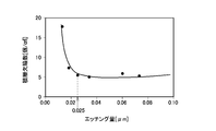
- FIG. 6 is a graph showing the relationship between the etching rate and the number of stacking faults (pieces / cm 2 ) generated on an epitaxial wafer when the etching amount with hydrogen chloride gas is fixed at 0.5 ⁇ m. It is a graph which shows the relationship between the etching amount when the etching rate by hydrogen chloride gas is fixed to 0.090 ⁇ m / min, and the number of stacking faults (pieces / cm 2 ) generated in the epitaxial wafer.
- a single wafer type vapor phase growth apparatus is an apparatus in which substrates are loaded one by one and an epitaxial layer is formed on the main surface of the loaded single substrate by vapor phase growth.
- the vapor phase growth apparatus is disposed so as to surround a reaction furnace in which a substrate to be processed is loaded, a susceptor that is disposed in the reaction furnace and horizontally supports the loaded substrate, and the reaction furnace.
- a heater for heating the inside of the reaction furnace and a temperature measuring unit for measuring the temperature of the substrate disposed in the reaction furnace are configured.
- the susceptor is provided so as to be rotatable about its central axis, and the susceptor rotates during vapor phase growth.
- a gas supply port for supplying various gases onto the surface of the substrate in the reaction furnace is formed on one end side of the reaction furnace.
- the gas supplied from the gas supply port is silicon source gas, carrier gas (for example, hydrogen gas), dopant gas for adjusting the conductivity type and conductivity of the epitaxial layer, and the like.
- a gas discharge port for discharging the gas that has passed over the surface of the substrate is formed on the opposite side of the reaction furnace from the gas supply port.
- the heater can be, for example, a halogen lamp provided above and below the reactor.
- the temperature measurement unit can be, for example, a pyrometer (radiation thermometer) that measures the surface temperature of the substrate without contacting the substrate.
- a silicon single crystal substrate serving as a growth substrate on which an epitaxial layer is vapor-phase grown is manufactured.
- a silicon single crystal ingot is produced by immersing and pulling up a seed crystal silicon rod on the surface of a melt obtained by adding polycrystalline silicon and red phosphorus for adjusting resistivity in a quartz crucible and melting it.
- the produced silicon single crystal ingot is cut out to a predetermined thickness, and a silicon single crystal substrate obtained by subjecting the cut wafer to rough polishing, etching, polishing and the like is produced.
- This silicon single crystal substrate is adjusted to have a resistivity of, for example, 1.4 m ⁇ ⁇ cm or less by red phosphorus added as a dopant when the silicon single crystal ingot is manufactured.
- the resistivity of the silicon single crystal substrate is 1.4 m ⁇ ⁇ cm. That is, the resistivity of the silicon single crystal substrate can be made 1.4 m ⁇ ⁇ cm or less by adjusting the red phosphorus concentration in the silicon single crystal substrate to 5 ⁇ 10 19 atoms / cm 3 or more.
- the amount of red phosphorus to be added may be adjusted so that the resistivity becomes 0.85 m ⁇ ⁇ cm or less, for example.
- the silicon single crystal ingot that is the basis of the silicon single crystal substrate is not limited to the CZ method, and may be obtained by other methods such as the FZ method.
- the produced silicon single crystal substrate is put into a reactor of a vapor phase growth apparatus and placed on a susceptor. At this time, hydrogen gas is supplied as atmospheric gas in the reactor.
- the temperature of the silicon single crystal substrate is heated by the heater so that the temperature of the silicon single crystal substrate is increased at a constant rate of temperature, and is suitable for vapor phase etching of the silicon single crystal substrate (for example, 1050 ° C. to 1200 ° C.). Heat until.
- the power of the heater is adjusted based on the measurement value of the temperature measurement unit provided in the vapor phase growth apparatus.
- an etching process for performing vapor phase etching on the main surface of the silicon single crystal substrate while maintaining the temperature of the silicon single crystal substrate.
- HCl gas hydrogen chloride gas
- the vapor-phase etching rate is preferably set to 0.04 ⁇ m / min or more and 0.37 ⁇ m / min or less.
- the etching rate can be adjusted by the flow rate and concentration of hydrogen chloride gas.
- concentration of the hydrogen chloride gas can be adjusted based on, for example, the flow rate of the hydrogen chloride gas and the flow rate of the dilution gas (for example, hydrogen gas) supplied into the reaction furnace together with the hydrogen chloride gas.
- the etching amount of the silicon single crystal substrate is set to 0.025 ⁇ m or more and 1.000 ⁇ m or less based on the direction from the main surface of the silicon single crystal substrate to the depth direction of the silicon single crystal substrate. It is preferable to set. By setting the etching amount to this condition, the number of stacking faults generated in the silicon epitaxial wafer can be reduced as shown in the following examples.
- the etching amount can be adjusted based on, for example, the supply time and flow rate of hydrogen chloride gas.
- a purging process for discharging hydrogen chloride gas from the reactor is performed.
- the supply of hydrogen chloride gas to the reaction furnace is stopped and hydrogen gas is supplied into the reaction furnace.
- the supply time of the hydrogen gas that is, the purge time may be appropriately set so that the hydrogen chloride gas does not remain in the reaction furnace after the purge process, but can be set to, for example, 30 seconds or more.
- the temperature in the reaction furnace (the temperature of the silicon single crystal substrate) may be maintained at the temperature in the previous vapor phase etching or may be different from the temperature in the vapor phase etching.
- the power of the heater is adjusted to bring the temperature of the silicon single crystal substrate to a growth temperature (for example, 1050 ° C. to 1200 ° C.) for vapor phase growth of the epitaxial layer.
- the main surface of the silicon single crystal substrate is a silicon source gas, for example, trichlorosilane (TCS), a hydrogen gas that is a carrier gas for diluting the trichlorosilane, and the resistivity and conductivity type of the epitaxial layer are adjusted.
- a dopant gas for example, PH 3
- PH 3 is supplied to grow a silicon epitaxial layer (silicon single crystal film) on the main surface of the silicon single crystal substrate.
- the vapor phase growth conditions may be appropriately set according to the conditions (film thickness, resistivity, etc.) of the epitaxial layer to be formed.
- the resistivity of the epitaxial layer may be set to 1.4 m ⁇ ⁇ cm or less as in the case of the resistivity of the silicon single crystal substrate, or may be set to a value greater than 1.4 m ⁇ ⁇ cm.
- the temperature inside the reactor is lowered at a constant rate, and the manufactured silicon epitaxial wafer is taken out of the reactor. From the above, a low resistance silicon epitaxial wafer is obtained.
- the main surface of the silicon single crystal substrate is subjected to gas phase etching with hydrogen chloride gas before vapor phase growth, stacking fault nuclei existing on the main surface can be removed.
- the etching rate is set to 0.04 ⁇ m / min or more and 0.37 ⁇ m / min or less, and the etching amount is set to 0.025 ⁇ m or more and 1.000 ⁇ m or less.
- the number of stacking faults generated in the silicon epitaxial wafer can be greatly reduced. Further, since the number of stacking faults can be reduced without performing any special process other than vapor phase etching, it is possible to suppress the complexity of the manufacturing process of the silicon epitaxial wafer.
- FIG. 1 shows the relationship between the etching rate of vapor-phase etching with hydrogen chloride gas and the stacking fault concentration on the main surface of the wafer when an epitaxial layer is vapor-grown on a low-resistance silicon single crystal substrate subjected to this vapor-phase etching. Is shown.
- the horizontal axis shows the etching rate of vapor phase etching with hydrogen chloride gas
- the vertical axis shows the number of stacking faults per unit area generated on the main surface of the epitaxial wafer measured by a particle counter (MAGICS manufactured by Lasertec Corporation). Show.
- the number of stacking faults on the vertical axis is a value converted to the number per unit area by obtaining the number of stacking faults per wafer and dividing the number of stacking faults by the surface area of the wafer.
- a silicon single crystal substrate having a red phosphorus concentration of 1.0 ⁇ 10 20 atoms / cm 3 , a resistivity of 0.75 m ⁇ ⁇ cm, and a diameter of 200 mm was used.
- the etching amount in the gas phase etching is 0.5 ⁇ m, and purging is performed for 30 seconds for the purpose of discharging the hydrogen chloride gas from the chamber after the etching, and then the main surface of the silicon single crystal substrate A 4.0 [mu] m silicon epitaxial layer was vapor-phase grown thereon.
- the number of stacking faults takes the minimum value at point A where the etching rate is 0.090 ⁇ m / min, and the number of stacking faults that reaches the minimum value is 4.9 pieces / cm 2 .
- the number of stacking faults increases almost in proportion to the increase in the etching rate.
- the number of stacking faults was 9.6 / cm 2 , which is about twice that of point A (slightly less than twice).
- the number of stacking faults is greater than 9.6 / cm 2 .
- the number of stacking faults increases rapidly as the etching rate decreases, and when the etching rate is 0.015 ⁇ m / min, the number of stacking faults is 50 / cm 2. It increased to the above. Further, at point C where the etching rate was 0.037 ⁇ m / min, the number of stacking faults was 8.8 pieces / cm 2 , which is about twice that of point A (slightly less than twice). When the etching rate is smaller than 0.037 ⁇ m / min, the number of stacking faults is more than 8.8 / cm 2 .
- the effect of reducing the number of stacking faults can be improved by setting the etching rate in the vapor phase etching in the vicinity of 0.090 ⁇ m / min. Specifically, by setting the etching rate to 0.037 ⁇ m / min or more and 0.371 ⁇ m / min or less, the number of stacking faults is set to a value near the minimum value (4.9 pieces / cm 2 ) (the minimum value of 2). (A value less than double). In other words, by setting the etching rate to 0.037 ⁇ m / min or more and 0.371 ⁇ m / min or less, the number of stacking faults can be suppressed to 10 pieces / cm 2 or less.
- a silicon epitaxial wafer with a reduced number of stacking faults can be manufactured by performing vapor phase etching at an etching rate of 0.04 ⁇ m / min or more and 0.37 ⁇ m / min or less.
- FIG. 2 shows the relationship between the etching amount of vapor phase etching using hydrogen chloride gas and the concentration of stacking faults on the main surface of the wafer when the epitaxial layer is vapor grown on the low resistance silicon single crystal substrate subjected to the vapor phase etching. Is shown.
- the horizontal axis shows the etching amount of gas phase etching with hydrogen chloride gas
- the vertical axis shows the number of stacking faults per unit area generated on the main surface of the epitaxial wafer measured by a particle counter (MAGICS manufactured by Lasertec Corporation). Show.
- the number of stacking faults on the vertical axis is a value converted to the number per unit area by obtaining the number of stacking faults per wafer and dividing the number of stacking faults by the surface area of the wafer.
- a silicon single crystal substrate having a red phosphorus concentration of 1.0 ⁇ 10 20 atoms / cm 3 , a resistivity of 0.75 m ⁇ ⁇ cm, and a diameter of 200 mm was used.
- the etching rate in the vapor phase etching is set to 0.090 ⁇ m / min at which the number of stacking faults is minimized in the first embodiment.
- purging for discharging hydrogen chloride gas from the chamber was performed for 30 seconds, and then a 4.0 ⁇ m silicon epitaxial layer was vapor grown on the main surface of the silicon single crystal substrate.
- the etching amount in the region where the etching amount is smaller than 0.025 ⁇ m, the number of stacking faults increases, and the number of stacking faults increases rapidly as the etching amount decreases.
- the etching amount is 0.025 ⁇ m or more, the number of stacking faults converges to a constant value (about 5 / cm 2 ).
- This result indicates that an etching amount of 0.025 ⁇ m or more is required for cleaning the substrate surface for the purpose of suppressing stacking faults, and the stacking fault nucleus is 0.025 ⁇ m or more deep from the substrate surface. It is considered to be localized in the region.
- the etching amount exceeds 1.000 ⁇ m, the productivity is lowered. Therefore, the etching amount is preferably 1.000 ⁇ m or less.
- the etching amount in the gas phase etching is preferably 0.025 ⁇ m or more and 1.000 ⁇ m or less. This makes it possible to effectively remove stacking fault nuclei on the main surface of the silicon single crystal substrate, and as a result, a silicon epitaxial wafer with a reduced number of stacking faults can be obtained.
- the present invention is not limited to the above embodiment.
- the above-described embodiment is an exemplification, and the present invention has the same configuration as the technical idea described in the claims of the present invention and exhibits the same function and effect regardless of the present invention. It is included in the technical scope of the invention.
Landscapes
- Chemical & Material Sciences (AREA)
- Engineering & Computer Science (AREA)
- Materials Engineering (AREA)
- Metallurgy (AREA)
- Organic Chemistry (AREA)
- Chemical Kinetics & Catalysis (AREA)
- General Chemical & Material Sciences (AREA)
- Crystallography & Structural Chemistry (AREA)
- Mechanical Engineering (AREA)
- Inorganic Chemistry (AREA)
- Chemical Vapour Deposition (AREA)
- Crystals, And After-Treatments Of Crystals (AREA)
Abstract
シリコンエピタキシャル層の気相成長シーケンスにおいて、赤燐のドープにより抵抗率が1.4mΩ・cm以下に調整されたシリコン単結晶基板を準備し、そのシリコン単結晶基板の表面改質を目的として、シリコン単結晶基板表面を塩化水素ガスにより気相エッチングする。このとき、塩化水素ガスによる基板のエッチングレートを0.04μm/min以上、かつ0.37μm/min以下に制御する。また、エッチング量を0.025μm以上、かつ1.000μm以下に制御する。気相エッチングの後、シリコン単結晶基板の主表面上にシリコンエピタキシャル層を気相成長により形成する。これにより、低抵抗率のシリコン単結晶基板の主表面上にシリコンエピタキシャル層を気相成長させる方法において、積層欠陥数を低減したシリコンエピタキシャルウェーハを得ることができる方法を提供する。
Description
本発明は、低抵抗シリコンエピタキシャルウェーハの製造方法に関する。
モバイル端末等に用いる半導体素子にエピタキシャルウェーハが用いられる。モバイル端末の省電力化を目的に、このようなウェーハには高濃度にドーパントをドープした低抵抗率のシリコン単結晶基板にエピタキシャル層を気相成長させた低抵抗率のエピタキシャルウェーハが必要とされる。このエピタキシャルウェーハの元になるシリコン単結晶基板は、高濃度のドーパントをドープして引き上げたインゴットから作製されるが、引き上げの際にドープしたドーパントが蒸発してしまう。そのため、エピタキシャル層を気相成長させるシリコン単結晶基板がn型ならば、揮発性が比較的低い赤燐(リン)をドーパントとしてドープしたシリコン単結晶基板が用いられる。そして、このようなシリコン単結晶基板の主表面上にエピタキシャル層を気相成長することにより、低抵抗のエピタキシャルウェーハが製造される。
しかし、高濃度に赤燐がドープされた低抵抗率のシリコン単結晶基板にエピタキシャル層を気相成長すると、気相成長後のエピタキシャルウェーハの主表面に多くの積層欠陥(スタッキングフォルト)が発生する(例えば特許文献1参照)。この積層欠陥が発生したエピタキシャルウェーハを用いて半導体素子を作製すると、半導体素子(デバイス)の特性が低下してしまう。そのため、積層欠陥の発生数をデバイス特性に影響のない水準まで低減する必要がある。
エピタキシャルウェーハの主表面で観察される積層欠陥は、低抵抗率のシリコン単結晶基板上で発生した結晶欠陥等がエピタキシャルウェーハの主表面に伝搬することで観察される。そのため、積層欠陥の発生には、低抵抗率のシリコン単結晶基板における基板表面の状態が影響すると考えられている。
そこで、低抵抗率のシリコン単結晶基板にエピタキシャル層を気相成長する前に、そのシリコン単結晶基板の主表面を塩化水素ガスで気相エッチングして基板表面を清浄化し、積層欠陥の発生を抑制する対策が採られている。
ここで従来技術として、特許文献2には、高濃度にリンが埋込されたシリコンウェーハ表面を塩化水素ガスによりエッチングを行った後にエピタキシャル層を気相成長することが記載されている。
しかし、このような気相エッチング処理が施された低抵抗率のシリコン単結晶基板に気相成長をしても、依然として半導体素子の特性に悪影響を及ぼす濃度の積層欠陥がエピタキシャルウェーハに発生する。
本発明は上記事情に鑑みてなされ、低抵抗率のシリコン単結晶基板の主表面上にシリコンエピタキシャル層を気相成長させる方法において、積層欠陥数を低減したシリコンエピタキシャルウェーハを得ることができる方法を提供することを課題とする。
上記課題を解決するため、本発明は、抵抗率が1.4mΩ・cm以下のシリコン単結晶基板の主表面上にシリコンエピタキシャル層を気相成長させる方法において、エピタキシャル層の気相成長前に前記シリコン単結晶基板の主表面を塩化水素ガスにより0.04μm/min以上、かつ0.37μm/min以下のエッチングレートで気相エッチングすることを特徴とする。
この気相エッチングによりシリコン単結晶基板の主表面を清浄化できる。すなわち、エピタキシャルウェーハに積層欠陥を発生させる起点となる結晶欠陥等(以下、積層欠陥核という)をシリコン単結晶基板の主表面から除去することができる。さらに、気相エッチングにおけるエッチングレートを上記条件に限定することにより、積層欠陥数を低減したシリコンエピタキシャルウェーハが製造可能である。
また、本発明において、シリコン単結晶基板は赤燐が5×10¹⁹atoms/cm3以上ドープされている。これによって、シリコン単結晶基板の抵抗率を1.4mΩ・cm以下とすることができる。
また、気相エッチングにおけるエッチング量が0.025μm以上、かつ1.000μm以下とするのが好ましい。本発明者はエッチング量を0.025μm以上にすると積層欠陥の発生数を抑えることができることを確認している。また、生産性の観点で、エッチング量は1.000μm以下とするのが良い。
以下、図面を参照して、本発明に係る実施の形態について説明する。先ず、シリコンエピタキシャルウェーハの製造装置の一例として、枚葉式の気相成長装置の概略構成を説明する。
枚葉式の気相成長装置は、基板が1枚ずつ投入されて、投入された1枚の基板の主表面上に気相成長によりエピタキシャル層を形成する装置である。詳しくは、気相成長装置は、処理対象となる基板が投入される反応炉と、反応炉内に配置されて投入された基板を水平に支持するサセプタと、反応炉を囲むように配置されて反応炉内を加熱するヒータと、反応炉内に配置された基板の温度を計測する温度計測部とを含んで構成される。なお、サセプタはその中心軸線回りに回転可能に設けられて、気相成長の際にはサセプタは回転する。
反応炉の一端側には、反応炉内の基板の表面上に各種ガスを供給するためのガス供給口が形成されている。ガス供給口から供給されるガスは、シリコンソースガス、キャリアガス(例えば水素ガス)、エピタキシャル層の導電型や導電率を調整するためのドーパントガスなどである。反応炉の、ガス供給口と反対側には、基板の表面上を通過したガスを排出するためのガス排出口が形成されている。ヒータは、例えば反応炉の上下それぞれに設けられたハロゲンランプとすることができる。温度計測部は、例えば基板の表面温度を基板に非接触で計測するパイロメータ(放射温度計)とすることができる。
次に、シリコンエピタキシャルウェーハの製造方法を説明する。先ず、エピタキシャル層を気相成長させる成長用基板となるシリコン単結晶基板を作製する。例えば、石英るつぼに多結晶シリコンと抵抗率を調整するための赤燐を入れて溶融させた溶融液の液面に種結晶シリコン棒を漬けて引き上げ、シリコン単結晶インゴットを作製する。次に、作製したシリコン単結晶インゴットを所定の厚さに切り出し、切り出したウェーハに粗研磨、エッチング、研磨等を施したシリコン単結晶基板を作製する。このシリコン単結晶基板は、シリコン単結晶インゴットの作製時にドーパントとして添加した赤燐により抵抗率が、例えば、1.4mΩ・cm以下となるように調整される。シリコン単結晶基板における赤燐濃度が5×10¹⁹atoms/cm3の場合に、シリコン単結晶基板の抵抗率が1.4mΩ・cmとなる。つまり、シリコン単結晶基板における赤燐濃度を5×1019atoms/cm3以上に調整することで、シリコン単結晶基板の抵抗率を1.4mΩ・cm以下にできる。なお、さらに抵抗率が低いシリコン単結晶基板を得るために、例えば抵抗率が0.85mΩ・cm以下となるよう、添加する赤燐の量を調整しても良い。なお、シリコン単結晶基板のもとになるシリコン単結晶インゴットは、CZ法に限らず、FZ法など他の方法で得るようにしてもよい。
次に、作製されたシリコン単結晶基板を、気相成長装置の反応炉に投入して、サセプタ上に載置する。このとき、反応炉内は雰囲気ガスとして水素ガスが供給されている。
次に、ヒータによりシリコン単結晶基板の温度が一定の昇温速度で昇温するように加熱して、シリコン単結晶基板を気相エッチングするのに適した温度(例えば、1050℃~1200℃)になるまで加熱する。このとき、例えば気相成長装置に備えられた上記温度計測部の計測値に基づいてヒータのパワーが調整される。
シリコン単結晶基板の温度が気相エッチングをするのに適した温度に到達すると、シリコン単結晶基板の温度を維持した状態で、シリコン単結晶基板の主表面に対して気相エッチングを施すエッチング工程を行う。エッチング工程では、反応炉内のシリコン単結晶基板の主表面上に塩化水素ガス(HClガス)を供給し、その塩化水素ガスによりシリコン単結晶基板の主表面を気相エッチングする。このとき、気相エッチングのレート(エッチング速度)を0.04μm/min以上、かつ0.37μm/min以下に設定するのが好ましい。エッチングレートをこの条件に設定することで、下記実施例で示すように、シリコンエピタキシャルウェーハに発生する積層欠陥数を低減できる。エッチングレートは塩化水素ガスの流量や濃度により調整できる。塩化水素ガスの濃度は、例えば塩化水素ガスの流量と塩化水素ガスとともに反応炉内に供給する希釈ガス(例えば水素ガス)の流量とに基づいて調整できる。
また、気相エッチングにおいては、シリコン単結晶基板の主表面からシリコン単結晶基板の深さ方向に向かう方向を基準に、シリコン単結晶基板のエッチング量を0.025μm以上、かつ1.000μm以下に設定するのが好ましい。エッチング量をこの条件に設定することで、下記実施例で示すように、シリコンエピタキシャルウェーハに発生する積層欠陥数を低減できる。エッチング量は、例えば塩化水素ガスの供給時間や流量に基づいて調整できる。
エッチング工程が終了すると、次に、塩化水素ガスを反応炉から排出することを目的としたパージ工程を行う。このパージ工程においては、反応炉への塩化水素ガスの供給を停止するとともに、反応炉内に水素ガスを供給する。このとき、水素ガスの供給時間つまりパージ時間は、パージ工程後に反応炉に塩化水素ガスが残留しないよう適宜に設定すれば良いが、例えば30秒以上とすることができる。また、反応炉内の温度(シリコン単結晶基板の温度)は、先の気相エッチングにおける温度を維持しても良いし、気相エッチングにおける温度と異なる温度としても良い。
パージ工程が終了すると、次に、ヒータのパワーを調整することで、シリコン単結晶基板の温度を、エピタキシャル層を気相成長させるための成長温度(例えば、1050℃~1200℃)にする。そして、シリコン単結晶基板の主表面にシリコンソースガスとなる、例えば、トリクロロシラン(TCS)と、そのトリクロロシランを希釈するキャリアガスとなる水素ガスと、エピタキシャル層の抵抗率や導電型を調整するためのドーパントガス(例えばPH3)とを供給し、シリコン単結晶基板の主表面上にシリコンエピタキシャル層(シリコン単結晶膜)を気相成長させる。このとき、気相成長の条件(成長時間、ガス流量等)は、形成するエピタキシャル層の条件(膜厚、抵抗率など)に応じて適宜に設定すれば良い。なお、エピタキシャル層の抵抗率は、シリコン単結晶基板の抵抗率と同様に1.4mΩ・cm以下に設定しても良いし、1.4mΩ・cmより大きい値に設定しても良い。
その後、反応炉内を一定の降温速度で降温した後、製造されたシリコンエピタキシャルウェーハを反応炉から取り出す。以上より、低抵抗シリコンエピタキシャルウェーハが得られる。
このように、本実施形態では、気相成長前に、シリコン単結晶基板の主表面を、塩化水素ガスにより気相エッチングを行うので、その主表面に存在していた積層欠陥核を除去できる。このとき、気相エッチングの条件として、エッチングレートを0.04μm/min以上、かつ0.37μm/min以下とし、かつ、エッチング量を0.025μm以上、かつ1.000μm以下とすることで、下記実施例で示すように、シリコンエピタキシャルウェーハに発生する積層欠陥数を大幅に低減できる。また、気相エッチング以外に特別な工程を実施しなくても積層欠陥数を低減できるので、シリコンエピタキシャルウェーハの製造工程が複雑になるのを抑制できる。
以下、実施例を挙げて本発明を具体的に説明するが、これらは本発明を限定するものではない。
(実施例1)
図1は、塩化水素ガスによる気相エッチングのエッチングレートと、この気相エッチングを施した低抵抗シリコン単結晶基板にエピタキシャル層を気相成長した際のウェーハ主表面上の積層欠陥濃度との関係を示している。横軸は、塩化水素ガスによる気相エッチングのエッチングレートを示し、縦軸は、パーティクルカウンタ(レーザーテック社製のMAGICS)により計測したエピタキシャルウェーハの主表面に発生した積層欠陥の単位面積当たりの個数を示している。なお、縦軸の積層欠陥数は、ウェーハ当たりの積層欠陥数を求め、その積層欠陥数をウェーハの表面積で除算することで、単位面積当たりの個数に換算した値である。
図1は、塩化水素ガスによる気相エッチングのエッチングレートと、この気相エッチングを施した低抵抗シリコン単結晶基板にエピタキシャル層を気相成長した際のウェーハ主表面上の積層欠陥濃度との関係を示している。横軸は、塩化水素ガスによる気相エッチングのエッチングレートを示し、縦軸は、パーティクルカウンタ(レーザーテック社製のMAGICS)により計測したエピタキシャルウェーハの主表面に発生した積層欠陥の単位面積当たりの個数を示している。なお、縦軸の積層欠陥数は、ウェーハ当たりの積層欠陥数を求め、その積層欠陥数をウェーハの表面積で除算することで、単位面積当たりの個数に換算した値である。
図1の実験では、赤燐濃度が1.0×10²⁰atoms/cm3、抵抗率が0.75mΩ・cm、直径が200mmのシリコン単結晶基板を用いた。また、図1の実験では、気相エッチングにおけるエッチング量は0.5μmとし、エッチング後に塩化水素ガスをチャンバーから排出することを目的としたパージを30秒間行い、次にシリコン単結晶基板の主表面上に4.0μmのシリコンエピタキシャル層を気相成長させた。
図1では、エッチングレートが0.090μm/minである点Aで積層欠陥数が最小値をとり、その最小値となる積層欠陥数は4.9個/cm2である。エッチングレートが0.090μm/minより大きい領域では、エッチングレートの増加にほぼ比例して積層欠陥数が増加している。そして、エッチングレートが0.371μm/minである点Bでは、積層欠陥数は点Aの約2倍(2倍より若干小さい)の9.6個/cm2となった。エッチングレートが0.371μm/minより大きくなると、積層欠陥数が9.6個/cm2より多くなる。
また、エッチングレートが0.090μm/minより小さい領域では、エッチングレートが小さいほど積層欠陥数が急激に増加し、エッチングレートが0.015μm/minの場合には積層欠陥数が50個/cm2以上にまで増加した。また、エッチングレートが0.037μm/minである点Cでは、積層欠陥数は点Aの約2倍(2倍より若干小さい)の8.8個/cm2となった。エッチングレートが0.037μm/minより小さいと、積層欠陥数は8.8個/cm2より多くなる。
このように、気相エッチングにおけるエッチングレートを0.090μm/min付近に設定することで積層欠陥数の低減効果を向上できる。詳しくは、エッチングレートを0.037μm/min以上、かつ0.371μm/min以下に設定することで、積層欠陥数を、最小値(4.9個/cm2)付近の値(最小値の2倍以下の値)に抑えることができる。別の言い方をすると、エッチングレートを0.037μm/min以上、かつ0.371μm/min以下に設定することで、積層欠陥数を10個/cm2以下に抑えることができる。0.037μm/min、0.371μm/minをそれぞれ小数第3位以下を四捨五入すると、それぞれ、0.04μm/min、0.37μm/minとなる。よって、0.04μm/min以上、かつ0.37μm/min以下のエッチングレートで気相エッチングを行うことで、積層欠陥数を低減したシリコンエピタキシャルウェーハを製造できる。
(実施例2)
図2は、塩化水素ガスによる気相エッチングのエッチング量と、この気相エッチングを施した低抵抗シリコン単結晶基板にエピタキシャル層を気相成長した際のウェーハ主表面上の積層欠陥濃度との関係を示している。横軸は、塩化水素ガスによる気相エッチングのエッチング量を示し、縦軸は、パーティクルカウンタ(レーザーテック社製のMAGICS)により計測したエピタキシャルウェーハの主表面に発生する積層欠陥の単位面積当たりの個数を示している。なお、縦軸の積層欠陥数は、ウェーハ当たりの積層欠陥数を求め、その積層欠陥数をウェーハの表面積で除算することで、単位面積当たりの個数に換算した値である。
図2は、塩化水素ガスによる気相エッチングのエッチング量と、この気相エッチングを施した低抵抗シリコン単結晶基板にエピタキシャル層を気相成長した際のウェーハ主表面上の積層欠陥濃度との関係を示している。横軸は、塩化水素ガスによる気相エッチングのエッチング量を示し、縦軸は、パーティクルカウンタ(レーザーテック社製のMAGICS)により計測したエピタキシャルウェーハの主表面に発生する積層欠陥の単位面積当たりの個数を示している。なお、縦軸の積層欠陥数は、ウェーハ当たりの積層欠陥数を求め、その積層欠陥数をウェーハの表面積で除算することで、単位面積当たりの個数に換算した値である。
図2の実験では、赤燐濃度が1.0×10²⁰atoms/cm3、抵抗率が0.75mΩ・cm、直径が200mmのシリコン単結晶基板を用いた。また、図2の実験では、気相エッチングにおけるエッチングレートを上記実施例1において積層欠陥の発生数が最小となる0.090μm/minとした。気相エッチング後に塩化水素ガスをチャンバーから排出することを目的としたパージを30秒間行い、次にシリコン単結晶基板の主表面上に4.0μmのシリコンエピタキシャル層を気相成長させた。
図2においてエッチング量が0.025μmより小さい領域では、積層欠陥の発生数が多くなっており、エッチング量が小さいほど積層欠陥数が急激に多くなる。エッチング量を0.025μm以上にすると積層欠陥数は一定値(約5個/cm2)に収束する。この結果は、積層欠陥の抑制を目的とした基板表面の清浄化には0.025μm以上のエッチング量が必要であることを示しており、積層欠陥核が基板表面から0.025μm以上の深さ領域に局在していると考えられる。また、エッチング量が1.000μmを超えると生産性が低下するため、エッチング量は1.000μm以下とするのが好ましい。
以上より、気相エッチングにおけるエッチング量は0.025μm以上、かつ1.000μm以下とするのが好ましい。これにより、シリコン単結晶基板の主表面における積層欠陥核を効果的に除去することが可能となり、その結果、積層欠陥数を低減したシリコンエピタキシャルウェーハを得ることができる。
なお、本発明は、上記実施形態に限定されるものではない。上記実施形態は、例示であり、本発明の請求の範囲に記載された技術的思想と実質的に同一な構成を有し、同様な作用効果を奏するものは、いかなるものであったとしても本発明の技術的範囲に包含される。
Claims (3)
- 抵抗率が1.4mΩ・cm以下のシリコン単結晶基板の主表面上にシリコンエピタキシャル層を気相成長させる方法において、エピタキシャル層の気相成長前に前記シリコン単結晶基板の主表面を塩化水素ガスにより0.04μm/min以上、かつ0.37μm/min以下のエッチングレートで気相エッチングすることを特徴とするシリコンエピタキシャルウェーハの製造方法。
- 前記シリコン単結晶基板は赤燐が5×10¹⁹atoms/cm3以上ドープされていることを特徴とする請求項1に記載のシリコンエピタキシャルウェーハの製造方法。
- 前記気相エッチングにおけるエッチング量が0.025μm以上、かつ1.000μm以下であることを特徴とする請求項1又は2に記載のシリコンエピタキシャルウェーハの製造方法。
Applications Claiming Priority (2)
| Application Number | Priority Date | Filing Date | Title |
|---|---|---|---|
| JP2016-074451 | 2016-04-01 | ||
| JP2016074451A JP6447960B2 (ja) | 2016-04-01 | 2016-04-01 | シリコンエピタキシャルウェーハの製造方法 |
Publications (1)
| Publication Number | Publication Date |
|---|---|
| WO2017169290A1 true WO2017169290A1 (ja) | 2017-10-05 |
Family
ID=59964134
Family Applications (1)
| Application Number | Title | Priority Date | Filing Date |
|---|---|---|---|
| PCT/JP2017/006249 Ceased WO2017169290A1 (ja) | 2016-04-01 | 2017-02-21 | シリコンエピタキシャルウェーハの製造方法 |
Country Status (2)
| Country | Link |
|---|---|
| JP (1) | JP6447960B2 (ja) |
| WO (1) | WO2017169290A1 (ja) |
Cited By (2)
| Publication number | Priority date | Publication date | Assignee | Title |
|---|---|---|---|---|
| JP2017005049A (ja) * | 2015-06-08 | 2017-01-05 | 信越半導体株式会社 | エピタキシャルウェーハの製造方法 |
| CN120311309A (zh) * | 2025-06-17 | 2025-07-15 | 中国电子科技集团公司第四十六研究所 | 一种半导体器件用双层厚膜高阻单晶外延片的制备方法 |
Families Citing this family (1)
| Publication number | Priority date | Publication date | Assignee | Title |
|---|---|---|---|---|
| CN111463115B (zh) * | 2020-04-27 | 2022-05-13 | 中国电子科技集团公司第四十六研究所 | 一种肖特基器件用硅外延片的制备方法 |
Citations (8)
| Publication number | Priority date | Publication date | Assignee | Title |
|---|---|---|---|---|
| JPS5398775A (en) * | 1977-02-09 | 1978-08-29 | Hitachi Ltd | Gas phase growth unit |
| JPS54141560A (en) * | 1978-04-21 | 1979-11-02 | Philips Nv | Method of forming epitaxial layer |
| JPH0472718A (ja) * | 1990-07-13 | 1992-03-06 | Nec Corp | エピタキシャル成長方法 |
| JPH05144751A (ja) * | 1991-11-22 | 1993-06-11 | Sony Corp | 半導体エピタキシヤル基板の製造方法 |
| JPH05166721A (ja) * | 1991-12-12 | 1993-07-02 | Mitsubishi Materials Corp | エピタキシャル層の形成方法 |
| JP2012114138A (ja) * | 2010-11-22 | 2012-06-14 | Sumco Corp | シリコンウェーハのエピタキシャル成長方法 |
| JP2014011293A (ja) * | 2012-06-29 | 2014-01-20 | Sumco Corp | エピタキシャルシリコンウェーハの製造方法、および、エピタキシャルシリコンウェーハ |
| JP2016213232A (ja) * | 2015-04-30 | 2016-12-15 | 株式会社Sumco | エピタキシャルシリコンウェーハの製造方法 |
-
2016
- 2016-04-01 JP JP2016074451A patent/JP6447960B2/ja active Active
-
2017
- 2017-02-21 WO PCT/JP2017/006249 patent/WO2017169290A1/ja not_active Ceased
Patent Citations (8)
| Publication number | Priority date | Publication date | Assignee | Title |
|---|---|---|---|---|
| JPS5398775A (en) * | 1977-02-09 | 1978-08-29 | Hitachi Ltd | Gas phase growth unit |
| JPS54141560A (en) * | 1978-04-21 | 1979-11-02 | Philips Nv | Method of forming epitaxial layer |
| JPH0472718A (ja) * | 1990-07-13 | 1992-03-06 | Nec Corp | エピタキシャル成長方法 |
| JPH05144751A (ja) * | 1991-11-22 | 1993-06-11 | Sony Corp | 半導体エピタキシヤル基板の製造方法 |
| JPH05166721A (ja) * | 1991-12-12 | 1993-07-02 | Mitsubishi Materials Corp | エピタキシャル層の形成方法 |
| JP2012114138A (ja) * | 2010-11-22 | 2012-06-14 | Sumco Corp | シリコンウェーハのエピタキシャル成長方法 |
| JP2014011293A (ja) * | 2012-06-29 | 2014-01-20 | Sumco Corp | エピタキシャルシリコンウェーハの製造方法、および、エピタキシャルシリコンウェーハ |
| JP2016213232A (ja) * | 2015-04-30 | 2016-12-15 | 株式会社Sumco | エピタキシャルシリコンウェーハの製造方法 |
Cited By (2)
| Publication number | Priority date | Publication date | Assignee | Title |
|---|---|---|---|---|
| JP2017005049A (ja) * | 2015-06-08 | 2017-01-05 | 信越半導体株式会社 | エピタキシャルウェーハの製造方法 |
| CN120311309A (zh) * | 2025-06-17 | 2025-07-15 | 中国电子科技集团公司第四十六研究所 | 一种半导体器件用双层厚膜高阻单晶外延片的制备方法 |
Also Published As
| Publication number | Publication date |
|---|---|
| JP6447960B2 (ja) | 2019-01-09 |
| JP2017188507A (ja) | 2017-10-12 |
Similar Documents
| Publication | Publication Date | Title |
|---|---|---|
| JP6945805B2 (ja) | エピタキシャルウェーハの製造方法 | |
| JP2015185653A (ja) | 炭化珪素半導体装置の製造方法 | |
| JP5786759B2 (ja) | エピタキシャル炭化珪素ウエハの製造方法 | |
| JP6447960B2 (ja) | シリコンエピタキシャルウェーハの製造方法 | |
| JP5780491B2 (ja) | シリコンエピタキシャルウェーハの製造方法 | |
| JP6358472B2 (ja) | エピタキシャルウェーハの製造方法 | |
| JP5589867B2 (ja) | シリコンエピタキシャルウェーハの製造方法 | |
| JP4838587B2 (ja) | 気相成長方法 | |
| JP6489321B2 (ja) | エピタキシャルウェーハの製造方法 | |
| JP6598140B2 (ja) | エピタキシャルウェーハの製造方法 | |
| TW201909246A (zh) | 晶圓製造方法和晶圓 | |
| JP6432879B2 (ja) | エピタキシャルウェーハの製造方法 | |
| JP4962406B2 (ja) | シリコン単結晶の育成方法 | |
| JP5315944B2 (ja) | シリコンエピタキシャルウェーハの製造方法 | |
| JP6372709B2 (ja) | エピタキシャルウェーハの製造方法 | |
| US20250051961A1 (en) | Method of manufacturing silicon epitaxial substrate and silicon epitaxial substrate | |
| JP4600086B2 (ja) | 多層のエピタキシャルシリコン単結晶ウェーハの製造方法及び多層のエピタキシャルシリコン単結晶ウェーハ | |
| JP6369388B2 (ja) | シリコン単結晶基板の評価方法 | |
| WO2025033083A1 (ja) | シリコンウェーハ及びその製造方法 | |
| JP2018157138A (ja) | エピタキシャルウェーハの製造方法 | |
| JP2013045805A (ja) | シリコンエピタキシャルウェーハの製造方法 | |
| JP2008169109A (ja) | 単結晶、単結晶ウエーハ及びエピタキシャルウエーハ | |
| WO2022172368A1 (ja) | シリコン単結晶の製造方法 | |
| JP2014013835A (ja) | シリコンエピタキシャルウェーハの製造方法 | |
| JP2010199356A (ja) | シリコンエピタキシャルウェーハおよびシリコンエピタキシャルウェーハの製造方法 |
Legal Events
| Date | Code | Title | Description |
|---|---|---|---|
| NENP | Non-entry into the national phase |
Ref country code: DE |
|
| 121 | Ep: the epo has been informed by wipo that ep was designated in this application |
Ref document number: 17773838 Country of ref document: EP Kind code of ref document: A1 |
|
| 122 | Ep: pct application non-entry in european phase |
Ref document number: 17773838 Country of ref document: EP Kind code of ref document: A1 |