WO2017164386A1 - ワイヤボンディング装置、ワイヤボンディング装置用回路並びに半導体装置の製造方法 - Google Patents
ワイヤボンディング装置、ワイヤボンディング装置用回路並びに半導体装置の製造方法 Download PDFInfo
- Publication number
- WO2017164386A1 WO2017164386A1 PCT/JP2017/012080 JP2017012080W WO2017164386A1 WO 2017164386 A1 WO2017164386 A1 WO 2017164386A1 JP 2017012080 W JP2017012080 W JP 2017012080W WO 2017164386 A1 WO2017164386 A1 WO 2017164386A1
- Authority
- WO
- WIPO (PCT)
- Prior art keywords
- wire
- spool
- changeover switch
- relay
- stick
- Prior art date
- Legal status (The legal status is an assumption and is not a legal conclusion. Google has not performed a legal analysis and makes no representation as to the accuracy of the status listed.)
- Ceased
Links
Images


Classifications
-
- H—ELECTRICITY
- H10—SEMICONDUCTOR DEVICES; ELECTRIC SOLID-STATE DEVICES NOT OTHERWISE PROVIDED FOR
- H10W—GENERIC PACKAGES, INTERCONNECTIONS, CONNECTORS OR OTHER CONSTRUCTIONAL DETAILS OF DEVICES COVERED BY CLASS H10
- H10W72/00—Interconnections or connectors in packages
- H10W72/071—Connecting or disconnecting
- H10W72/0711—Apparatus therefor
-
- H—ELECTRICITY
- H10—SEMICONDUCTOR DEVICES; ELECTRIC SOLID-STATE DEVICES NOT OTHERWISE PROVIDED FOR
- H10W—GENERIC PACKAGES, INTERCONNECTIONS, CONNECTORS OR OTHER CONSTRUCTIONAL DETAILS OF DEVICES COVERED BY CLASS H10
- H10W72/00—Interconnections or connectors in packages
- H10W72/071—Connecting or disconnecting
- H10W72/075—Connecting or disconnecting of bond wires
-
- H—ELECTRICITY
- H10—SEMICONDUCTOR DEVICES; ELECTRIC SOLID-STATE DEVICES NOT OTHERWISE PROVIDED FOR
- H10W—GENERIC PACKAGES, INTERCONNECTIONS, CONNECTORS OR OTHER CONSTRUCTIONAL DETAILS OF DEVICES COVERED BY CLASS H10
- H10W72/00—Interconnections or connectors in packages
- H10W72/50—Bond wires
-
- H—ELECTRICITY
- H10—SEMICONDUCTOR DEVICES; ELECTRIC SOLID-STATE DEVICES NOT OTHERWISE PROVIDED FOR
- H10W—GENERIC PACKAGES, INTERCONNECTIONS, CONNECTORS OR OTHER CONSTRUCTIONAL DETAILS OF DEVICES COVERED BY CLASS H10
- H10W72/00—Interconnections or connectors in packages
- H10W72/01—Manufacture or treatment
- H10W72/015—Manufacture or treatment of bond wires
- H10W72/01551—Changing the shapes of bond wires
-
- H—ELECTRICITY
- H10—SEMICONDUCTOR DEVICES; ELECTRIC SOLID-STATE DEVICES NOT OTHERWISE PROVIDED FOR
- H10W—GENERIC PACKAGES, INTERCONNECTIONS, CONNECTORS OR OTHER CONSTRUCTIONAL DETAILS OF DEVICES COVERED BY CLASS H10
- H10W72/00—Interconnections or connectors in packages
- H10W72/071—Connecting or disconnecting
- H10W72/0711—Apparatus therefor
- H10W72/07139—Means for protection against electrical discharge
-
- H—ELECTRICITY
- H10—SEMICONDUCTOR DEVICES; ELECTRIC SOLID-STATE DEVICES NOT OTHERWISE PROVIDED FOR
- H10W—GENERIC PACKAGES, INTERCONNECTIONS, CONNECTORS OR OTHER CONSTRUCTIONAL DETAILS OF DEVICES COVERED BY CLASS H10
- H10W72/00—Interconnections or connectors in packages
- H10W72/071—Connecting or disconnecting
- H10W72/0711—Apparatus therefor
- H10W72/07141—Means for applying energy, e.g. ovens or lasers
-
- H—ELECTRICITY
- H10—SEMICONDUCTOR DEVICES; ELECTRIC SOLID-STATE DEVICES NOT OTHERWISE PROVIDED FOR
- H10W—GENERIC PACKAGES, INTERCONNECTIONS, CONNECTORS OR OTHER CONSTRUCTIONAL DETAILS OF DEVICES COVERED BY CLASS H10
- H10W72/00—Interconnections or connectors in packages
- H10W72/071—Connecting or disconnecting
- H10W72/0711—Apparatus therefor
- H10W72/07168—Means for storing or moving the material for the connector
-
- H—ELECTRICITY
- H10—SEMICONDUCTOR DEVICES; ELECTRIC SOLID-STATE DEVICES NOT OTHERWISE PROVIDED FOR
- H10W—GENERIC PACKAGES, INTERCONNECTIONS, CONNECTORS OR OTHER CONSTRUCTIONAL DETAILS OF DEVICES COVERED BY CLASS H10
- H10W72/00—Interconnections or connectors in packages
- H10W72/071—Connecting or disconnecting
- H10W72/0711—Apparatus therefor
- H10W72/07183—Means for monitoring
-
- H—ELECTRICITY
- H10—SEMICONDUCTOR DEVICES; ELECTRIC SOLID-STATE DEVICES NOT OTHERWISE PROVIDED FOR
- H10W—GENERIC PACKAGES, INTERCONNECTIONS, CONNECTORS OR OTHER CONSTRUCTIONAL DETAILS OF DEVICES COVERED BY CLASS H10
- H10W72/00—Interconnections or connectors in packages
- H10W72/071—Connecting or disconnecting
- H10W72/075—Connecting or disconnecting of bond wires
- H10W72/07511—Treating the bonding area before connecting, e.g. by applying flux or cleaning
-
- H—ELECTRICITY
- H10—SEMICONDUCTOR DEVICES; ELECTRIC SOLID-STATE DEVICES NOT OTHERWISE PROVIDED FOR
- H10W—GENERIC PACKAGES, INTERCONNECTIONS, CONNECTORS OR OTHER CONSTRUCTIONAL DETAILS OF DEVICES COVERED BY CLASS H10
- H10W72/00—Interconnections or connectors in packages
- H10W72/071—Connecting or disconnecting
- H10W72/075—Connecting or disconnecting of bond wires
- H10W72/07521—Aligning
-
- H—ELECTRICITY
- H10—SEMICONDUCTOR DEVICES; ELECTRIC SOLID-STATE DEVICES NOT OTHERWISE PROVIDED FOR
- H10W—GENERIC PACKAGES, INTERCONNECTIONS, CONNECTORS OR OTHER CONSTRUCTIONAL DETAILS OF DEVICES COVERED BY CLASS H10
- H10W72/00—Interconnections or connectors in packages
- H10W72/50—Bond wires
- H10W72/531—Shapes of wire connectors
- H10W72/536—Shapes of wire connectors the connected ends being ball-shaped
-
- H—ELECTRICITY
- H10—SEMICONDUCTOR DEVICES; ELECTRIC SOLID-STATE DEVICES NOT OTHERWISE PROVIDED FOR
- H10W—GENERIC PACKAGES, INTERCONNECTIONS, CONNECTORS OR OTHER CONSTRUCTIONAL DETAILS OF DEVICES COVERED BY CLASS H10
- H10W72/00—Interconnections or connectors in packages
- H10W72/50—Bond wires
- H10W72/531—Shapes of wire connectors
- H10W72/5363—Shapes of wire connectors the connected ends being wedge-shaped
Definitions
- the present invention relates to a wire bonding apparatus, a structure of a circuit for a wire bonding apparatus, and a method for manufacturing a semiconductor device.
- wire bonding apparatuses that connect electrodes of devices such as semiconductor chips arranged on a circuit board and leads of the circuit board with metal wires are often used.
- a free air ball is formed by an electric torch at the tip of the wire, and after joining the free air ball to the electrode of the device by the capillary, the capillary is looped and the wire is pressed against the circuit board lead by the capillary, and then The wire is pulled up while being clamped by a clamper to cut the wire.
- a free air ball is formed by sandwiching a wire with a clamper, applying a high voltage for forming a free air ball to the wire, generating an electric discharge with the electric torch, and melting the wire.
- an object of the present invention is to suppress the electric corrosion of the wire clamper and detect non-sticking with a simple configuration.
- the wire bonding apparatus of the present invention includes a spool, a clamper that grips a wire fed out from the spool, a torch electrode that forms a free air ball at the tip of the wire by discharge, and a high-voltage power supply circuit that supplies power to the torch electrode
- a non-stick detection circuit for detecting non-stick between the wire and the device or the board, a first switch for switching connection between the spool and the high-voltage power supply circuit or the non-stick detection circuit, and a connection between the clamper and the spool side of the first switch.
- the wire bonding apparatus includes a second changeover switch that is disposed between the spool side of the first changeover switch and the spool, and that switches connection between the spool side of the first changeover switch and the ground line, and a control unit It is also preferable to check the continuity of the spool with the first changeover switch on the non-stick detection circuit side, the relay on, and the second changeover switch on the ground line side.
- a wire guide that is disposed between the spool and the clamper and has a through hole with which at least a part of the wire contacts, and a connection line that connects the wire guide and the spool side of the first changeover switch. It is also preferable to provide
- a circuit for a wire bonding apparatus includes a high-voltage power supply circuit that supplies power to a torch electrode that forms a free air ball at the tip of a wire by discharge, a non-stick detection circuit that detects non-stick between a wire and a device or a substrate, A first changeover switch for switching the connection between the spool for feeding the wire and the high-voltage power supply circuit or the non-stick detection circuit, and a relay for turning on / off the connection between the clamper for gripping the wire fed from the spool and the spool side of the first changeover switch And a control unit for setting the first changeover switch to the high voltage power supply circuit side and generating a discharge by turning off the relay, and setting the first changeover switch to the non-sticking detection circuit side and turning on the relay to detect non-sticking. It is characterized by that.
- a method of manufacturing a semiconductor device includes a spool, a clamper that grips a wire fed from the spool, a torch electrode that forms a free air ball at the tip of the wire by discharge, and a high-voltage power supply that supplies power to the torch electrode
- a non-stick detection circuit for detecting non-stick between a circuit, a wire and a device or a board, a first switch for switching connection between the spool and a high-voltage power supply circuit or a non-stick detection circuit, and a clamper and a spool side of the first switch
- a step of preparing a wire bonding apparatus including a relay for turning on / off the connection, and the first changeover switch on the high voltage power circuit side and the relay is turned off to supply electric power to the torch electrode and the free air ball And a wire on which a free air ball is formed is bonded to a device or a substrate.
- the present invention has a simple configuration and can suppress electric corrosion of the wire clamper and detect non-sticking.
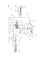
- the wire bonding apparatus 100 includes a spool 10, a clamper 22, a torch electrode 31, a high voltage power supply circuit 30, a non-sticking detection circuit 40, a first changeover switch 50, a relay 53, and a control. Part 60.
- the alternate long and short dash line indicates a signal line. The same applies to the other drawings.
- the spool 10 is provided with flanges at both ends of a cylindrical portion, a main body 11 around which a wire 21 is wound, a rotary shaft 12 connected to the main body 11, and a slip ring 13 attached to the rotary shaft 12.
- the terminal 15 is provided on the flange of the main body 11 and connected to the end 16 of the wire 21 wound around the cylindrical portion.
- a motor 14 that rotates the main body 11 is connected to the rotary shaft 12.
- the clamper 22 is attached between the spool 10 and the capillary 23.
- the clamper 22 is opened and closed by an opening / closing drive unit (not shown) to grip and release the wire 21.
- the torch electrode 31 is disposed in the vicinity of the wire 21 extending from the tip of the capillary 23, and discharge is generated between the tip of the wire 21 by the electric power supplied from the high-voltage power supply circuit 30. Free air balls 24 are formed.
- the torch electrode 31 protrudes to the vicinity of the tip of the wire 21 when the free air ball 24 is formed, and is pulled into a position away from the tip of the wire 21 in other cases.
- the non-sticking detection circuit 40 applies a voltage to the wire 21, and detects that the wire 21 and the device 19 are connected when the applied voltage decreases, and the voltage is applied even if the voltage is applied to the wire 21. If the drop does not decrease, non-bonding (connection failure) between the wire 21 and the device 19 on the substrate 18 connected to the ground is detected.
- the first changeover switch 50 is composed of two relays, a high voltage power supply circuit side relay 51 and a non-stick detection circuit side relay 52. By turning on one of the two relays and turning off the other, the connection between the spool 10 and the high voltage power supply circuit 30 or the non-sticking detection circuit 40 is switched.
- the plus terminal of the high voltage power supply circuit 30 is connected to the torch electrode 31 by a connection line 32.
- the ground-side terminal of the high-voltage power circuit 30 connected to the ground by the internal wiring 34 is connected to one end of the high-voltage power circuit-side relay 51 by the connection line 33.
- the other end of the high-voltage power circuit relay 51 is connected to the slip ring 13 of the spool 10 by the connection line 17.
- a terminal of the non-stick detection circuit 40 is connected to one end of the non-stick detection circuit side relay 52 by a connection line 41.
- the other end of the non-stick detection circuit side relay 52 is connected to the connection line 17.
- the connection line 17 and the clamper 22 are connected by a connection line 25 and are connected and released by a relay 53.
- the high-voltage power supply circuit 30, the non-stick detection circuit 40, the clamper 22 and the hook, the high-voltage power supply circuit-side relay 51, the non-stick detection circuit-side relay 52, the relay 53, and the motor 14 of the first changeover switch 50 are connected to the control unit 60. And is configured to operate according to a command from the control unit 60.
- the control unit 60 is a computer having a CPU 61 for performing information processing or calculation therein and a memory 62 for storing control programs and control data.
- the high-voltage power supply circuit 30, the non-stick detection circuit 40, the first changeover switch 50, the relay 53, and the control unit 60 constitute a wire bonding apparatus circuit (not shown).
- the control unit 60 turns on the high-voltage power supply circuit side relay 51 of the first changeover switch 50 and turns off the non-stick detection circuit side relay 52. Further, the control unit 60 turns off the relay 53 and closes the clamper 22. Then, the control unit 60 feeds the torch electrode 31 to the vicinity of the tip of the wire 21 extending from the tip of the capillary 23, and a high voltage is applied from the high voltage power supply circuit 30 to the torch electrode 31 as indicated by arrows 81 and 82 in FIG. Apply.
- a discharge is generated between the torch electrode 31 and the tip of the wire 21 due to the applied high voltage, and a free air ball 24 is formed at the tip of the wire 21. Further, the current flowing between the torch electrode 31 and the wire 21 due to the discharge flows from the end portion 16 of the wire 21 wound around the main body 11 of the spool 10 to the terminal 15 as shown by arrows 83 and 84 in FIG. The flow reaches the slip ring 13 from the flange portion of the main body 11 through the rotary shaft 12 as indicated by an arrow 85 in FIG. Then, as indicated by arrows 85 and 86 in FIG.
- the slip ring 13 passes through the connection line 17 and the high-voltage power circuit side relay 51, and passes through the connection line 33 as indicated by arrows 87 to 89 in FIG. It flows to the ground side terminal of the circuit 30 and flows to the ground as shown by the arrow 90 through the internal wiring 34.
- the wire bonding apparatus 100 when the free air ball 24 is formed, no current flows between the clamper 22 and the wire 21, and secondary discharge between the clamper 22 and the wire 21 does not occur. For this reason, the wire bonding apparatus 100 can suppress the electric contact of the clamper 22.
- a current flows from the non-contact detection circuit side relay 52 through the connection line 17 to the slip ring 13, and from the slip ring 13 to the rotating shaft 12, the terminal. 15, flows from the end portion 16 of the wire 21 to the wire 21 wound around the main body 11 of the spool 10 as indicated by an arrow 74 in FIG. 3. Then, as indicated by arrows 75 and 76, the current passes through the wire 21 in the straight portion and is bonded to the electrode of the device 19 through the wire 21 extending from the tip of the capillary 23 as indicated by the arrow 77. Flows into the press-bonded ball 24a. Then, it flows from the electrode of the device 19 to the ground.
- the tail wire 21a indicated by a one-dot chain line in FIG. 3 extends between the substrate 18 and the capillary 23.
- the controller 60 closes the clamper 22, pulls up the wire 21, and cuts the tail wire 21 a from the substrate 18.
- the controller 60 applies a voltage from the non-stick detection circuit 40 to the connection line 41 and detects non-stick between the substrate 18 and the wire 21 as described above.
- the clamper 22 since the clamper 22 is closed, in addition to the route described above, the clamper 22 passes from the connection line 17 through the relay 53 and the connection line 25 to the clamper 22 as indicated by arrows 78 and 79 in FIG.
- control unit 60 determines that the wire 21 and the substrate 18 are well connected when the voltage of the connection line 41 decreases, and conversely, when the applied voltage does not decrease. Then, it is determined that the connection between the wire 21 and the substrate 18 is defective and non-bonding has occurred, and a non-bonding detection signal is output.
- the first changeover switch 50 is set to the high-voltage power circuit side, the relay 53 is turned off, the free air ball 24 is formed, and the first changeover switch 50 is detected as non-attached. Since the non-adherence detection is performed by turning on the relay 53 on the circuit side, when the free air ball 24 is formed, the secondary discharge between the clamper 22 and the wire 21 is prevented and the contact of the clamper 22 is suppressed. Non-bonding detection between the wire 21 and the device 19 or the substrate 18 can be performed.
- the wire 21 is attached to the device 19 or the substrate 18 on the substrate 18 while suppressing the contact of the clamper 22 and detecting the non-bonding between the wire 21 and the device 19 or the substrate 18 by the process as described above.
- the semiconductor device in which the device 19 and the substrate 18 are connected by the wire 21 can be manufactured.
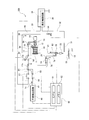
- the wire bonding apparatus 200 When non-bonding detection between the device 19 and the wire is performed by the wire bonding apparatus 100 described above, a current is passed through the spool 10 through the spool 10 by applying a detection voltage from the non-bonding detection circuit 40 to the connection line 41. Then, it flows from the press-bonded ball 24a to the ground. At this time, if the continuity of the slip ring 13 of the spool 10 is poor, the applied voltage does not decrease, and it is possible to erroneously detect non-adherence even though the wire 21 and the device 19 are connected. There is sex. Therefore, as shown in FIG. 4, the wire bonding apparatus 200 according to the present embodiment has the first changeover switch 50 connected to the connection line 17 of the wire bonding apparatus 100 described with reference to FIGS. 1 to 3.
- the second switch 54 for switching the connection between the spool side and the ground wire 55 is provided so that the conduction of the slip ring 13 of the spool 10 can be confirmed.
- the second changeover switch 54 is connected to the control unit 60 and operates according to a command from the control unit 60.
- the wire bonding apparatus 200 can determine whether the cause that the applied voltage does not decrease is due to non-bonding or due to poor conduction of the slip ring 13, suppresses false detection of non-bonding, and more reliably detects non-bonding. be able to.
- the control unit 60 switches the second changeover switch 54 to the ground line 55 side to make the connection line 17 and the ground line 55 conductive, and cuts off the connection between the connection line 17 and the spool side of the high-voltage power circuit relay 51. .
- the control unit 60 turns on the relay 53 and closes the clamper 22.
- the control unit 60 applies a detection voltage from the non-stick detection circuit 40 to the connection line 41 in the same manner as the previous non-stick detection operation.
- the detection voltage is applied, current flows from the non-stick detection circuit side relay 52 to the clamper 22 through the connection line 17 and the relay 53, as indicated by arrows 71, 91, 78, 79 in FIG.
- the current flows from the clamper 22 to the wire 21 and from the end portion 16 of the wire 21 wound around the main body 11 of the spool 10 to the terminal 15, and to the arrow 85 in FIG.
- the control unit 60 determines that the conduction of the slip ring 13 is normal. On the other hand, when the applied voltage does not decrease, it is determined that the conduction of the slip ring 13 is defective and a signal indicating the conduction failure of the slip ring 13 is output.
- the wire bonding apparatus 200 has the same effect as that of the wire bonding apparatus 100 described above, and the cause that the applied voltage does not decrease is due to non-attachment or the slip ring 13 is not conductive. It is possible to determine whether it is a non-sticky product, suppress erroneous detection of non-sticking, and more reliably detect non-sticking.
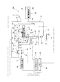
- wire bonding apparatus 300 is obtained by adding a wire guide 56 and a connection line 57 to the wire bonding apparatus 200 described above with reference to FIG.
- the wire guide 56 is disposed between the spool 10 and the clamper 22 and has a through hole with which at least a part of the wire 21 contacts.
- the wire guide 56 is made of metal.
- the wire guide 56 may be a blow-up portion that blows air from below to the through hole to apply an upward tension to the wire 21.
- the wire guide 56 is connected to the spool side of the first changeover switch 50 by a connection line 57.
- the conduction confirmation of the slip ring 13 in the wire bonding apparatus 300 will be described.
- the current from the non-stick detection circuit 40 flows from the spool side of the first changeover switch 50 to the wire guide 56 through the connection line 17 as indicated by arrows 95 and 96 in FIG. Since the wire guide 56 is in contact with the wire 21, current flows from the wire guide 56 to the wire 21, and from the spool 10 to the ground through the ground line 55 as described above with reference to FIG. 4. For this reason, the wire bonding apparatus 300 can check the conduction of the slip ring 13 even when the clamper 22 is in the open state.
- the wire bonding apparatus 300 can more reliably check the continuity of the slip ring 13 than the wire bonding apparatus 200 described above, and can more reliably erroneously detect non-bonding. Since this can be suppressed, non-stick detection can be performed more reliably.
Landscapes
- Wire Bonding (AREA)
- Testing Of Short-Circuits, Discontinuities, Leakage, Or Incorrect Line Connections (AREA)
Abstract
Description
Claims (5)
- ワイヤボンディング装置であって、
スプールと、
前記スプールから繰り出されたワイヤを把持するクランパと、
放電によって前記ワイヤの先端にフリーエアボールを形成するトーチ電極と、
前記トーチ電極に電力を供給する高圧電源回路と、
前記ワイヤとデバイスまたは基板との不着検出を行う不着検出回路と、
前記スプールと前記高圧電源回路または前記不着検出回路との接続を切換える第1切換えスイッチと、
前記クランパと前記第1切換えスイッチのスプール側との接続をオン/オフするリレーと、
前記第1切換えスイッチを高圧電源回路側とするとともに前記リレーをオフとして前記放電を発生させ、前記第1切換えスイッチを不着検出回路側とするとともに前記リレーをオンとして前記不着検出をさせる制御部と、を備えるワイヤボンディング装置。 - 請求項1に記載のワイヤボンディング装置であって、
前記第1切換えスイッチの前記スプール側と前記スプールとの間に配置され、前記第1切換えスイッチの前記スプール側と接地線との接続を切換える第2切換えスイッチと、を備え、
前記制御部は、前記第1切換えスイッチを前記不着検出回路側とするとともに前記リレーをオンとし、且つ、前記第2切換えスイッチを接地線側として前記スプールの導通確認を行うワイヤボンディング装置。 - 請求項2に記載のワイヤボンディング装置であって、
前記スプールと前記クランパとの間に配置され、前記ワイヤの少なくとも一部が接触する貫通孔を有するワイヤガイドと、
前記ワイヤガイドと前記第1切換えスイッチの前記スプール側とを接続する接続線と、を備えるワイヤボンディング装置。 - ワイヤボンディング装置用回路であって、
放電によってワイヤの先端にフリーエアボールを形成するトーチ電極に電力を供給する高圧電源回路と、
前記ワイヤとデバイスまたは基板との不着検出を行う不着検出回路と、
前記ワイヤを繰り出すスプールと前記高圧電源回路または前記不着検出回路との接続を切換える第1切換えスイッチと、
前記スプールから繰り出された前記ワイヤを把持するクランパと前記第1切換えスイッチのスプール側との接続をオン/オフするリレーと、
前記第1切換えスイッチを高圧電源回路側とするとともに前記リレーをオフとして前記放電を発生させるとともに、前記第1切換えスイッチを不着検出回路側とするとともに前記リレーをオンとして前記不着検出を行う制御部と、を備えるワイヤボンディング装置用回路。 - 半導体装置の製造方法であって、
スプールと、前記スプールから繰り出されたワイヤを把持するクランパと、放電によって前記ワイヤの先端にフリーエアボールを形成するトーチ電極と、前記トーチ電極に電力を供給する高圧電源回路と、前記ワイヤとデバイスまたは基板との不着検出を行う不着検出回路と、前記スプールと前記高圧電源回路または前記不着検出回路との接続を切換える第1切換えスイッチと、前記クランパと前記第1切換えスイッチのスプール側との接続をオン/オフするリレーとを備えるワイヤボンディング装置を準備する工程と、
前記第1切換えスイッチを高圧電源回路側とするとともに前記リレーをオフとして前記高圧電源回路が前記トーチ電極に電力を供給してフリーエアボールを形成する工程と、
前記フリーエアボールが形成された前記ワイヤをデバイス又は基板にボンディングする工程と、
前記第1切換えスイッチを不着検出回路側とするとともに前記リレーをオンとして、前記ワイヤと前記デバイス又は基板との前記不着検出をする工程とを含む、
半導体装置の製造方法。
Priority Applications (5)
| Application Number | Priority Date | Filing Date | Title |
|---|---|---|---|
| SG11201811528TA SG11201811528TA (en) | 2016-03-25 | 2017-03-24 | Wire bonding apparatus, circuit for wire bonding apparatus, and method for manufacturing semiconductor device |
| CN201780031626.0A CN109155260B (zh) | 2016-03-25 | 2017-03-24 | 引线接合装置、其电路以及半导体装置的制造方法 |
| US16/088,081 US10964661B2 (en) | 2016-03-25 | 2017-03-24 | Wire bonding apparatus, circuit for wire bonding apparatus, and method for manufacturing semiconductor device |
| KR1020187030659A KR102069565B1 (ko) | 2016-03-25 | 2017-03-24 | 와이어 본딩 장치, 와이어 본딩 장치용 회로 및 반도체 장치의 제조 방법 |
| JP2018507451A JP6676748B2 (ja) | 2016-03-25 | 2017-03-24 | ワイヤボンディング装置、ワイヤボンディング装置用回路並びに半導体装置の製造方法 |
Applications Claiming Priority (2)
| Application Number | Priority Date | Filing Date | Title |
|---|---|---|---|
| JP2016-061147 | 2016-03-25 | ||
| JP2016061147 | 2016-03-25 |
Publications (1)
| Publication Number | Publication Date |
|---|---|
| WO2017164386A1 true WO2017164386A1 (ja) | 2017-09-28 |
Family
ID=59899523
Family Applications (1)
| Application Number | Title | Priority Date | Filing Date |
|---|---|---|---|
| PCT/JP2017/012080 Ceased WO2017164386A1 (ja) | 2016-03-25 | 2017-03-24 | ワイヤボンディング装置、ワイヤボンディング装置用回路並びに半導体装置の製造方法 |
Country Status (7)
| Country | Link |
|---|---|
| US (1) | US10964661B2 (ja) |
| JP (1) | JP6676748B2 (ja) |
| KR (1) | KR102069565B1 (ja) |
| CN (1) | CN109155260B (ja) |
| SG (1) | SG11201811528TA (ja) |
| TW (1) | TWI639202B (ja) |
| WO (1) | WO2017164386A1 (ja) |
Citations (3)
| Publication number | Priority date | Publication date | Assignee | Title |
|---|---|---|---|---|
| JPH0794545A (ja) * | 1993-09-21 | 1995-04-07 | Shinkawa Ltd | ワイヤボンデイング装置 |
| JPH11243119A (ja) * | 1998-02-26 | 1999-09-07 | Power:Kk | ワイヤボンディング方法および装置 |
| JP2000306940A (ja) * | 1999-04-21 | 2000-11-02 | Shinkawa Ltd | バンプボンディングにおける不着検査方法及び装置 |
Family Cites Families (5)
| Publication number | Priority date | Publication date | Assignee | Title |
|---|---|---|---|---|
| JP3041812U (ja) | 1997-01-16 | 1997-10-03 | 義一 花本 | 開閉式拡大レンズ付き腕時計 |
| JP3908640B2 (ja) | 2002-09-26 | 2007-04-25 | 株式会社新川 | ワイヤボンディング方法及び装置 |
| JP3786281B2 (ja) * | 2004-11-05 | 2006-06-14 | 株式会社カイジョー | ワイヤボンディング装置 |
| JP4397326B2 (ja) * | 2004-12-27 | 2010-01-13 | 株式会社新川 | ボンディング装置 |
| JP4547330B2 (ja) * | 2005-12-28 | 2010-09-22 | 株式会社新川 | ワイヤボンディング装置、ボンディング制御プログラム及びボンディング方法 |
-
2017
- 2017-03-24 WO PCT/JP2017/012080 patent/WO2017164386A1/ja not_active Ceased
- 2017-03-24 JP JP2018507451A patent/JP6676748B2/ja active Active
- 2017-03-24 CN CN201780031626.0A patent/CN109155260B/zh not_active Expired - Fee Related
- 2017-03-24 KR KR1020187030659A patent/KR102069565B1/ko active Active
- 2017-03-24 US US16/088,081 patent/US10964661B2/en active Active
- 2017-03-24 TW TW106109850A patent/TWI639202B/zh active
- 2017-03-24 SG SG11201811528TA patent/SG11201811528TA/en unknown
Patent Citations (3)
| Publication number | Priority date | Publication date | Assignee | Title |
|---|---|---|---|---|
| JPH0794545A (ja) * | 1993-09-21 | 1995-04-07 | Shinkawa Ltd | ワイヤボンデイング装置 |
| JPH11243119A (ja) * | 1998-02-26 | 1999-09-07 | Power:Kk | ワイヤボンディング方法および装置 |
| JP2000306940A (ja) * | 1999-04-21 | 2000-11-02 | Shinkawa Ltd | バンプボンディングにおける不着検査方法及び装置 |
Also Published As
| Publication number | Publication date |
|---|---|
| TW201801207A (zh) | 2018-01-01 |
| CN109155260B (zh) | 2021-10-29 |
| KR20180125557A (ko) | 2018-11-23 |
| KR102069565B1 (ko) | 2020-01-23 |
| JP6676748B2 (ja) | 2020-04-08 |
| TWI639202B (zh) | 2018-10-21 |
| JPWO2017164386A1 (ja) | 2019-01-31 |
| US20200294957A1 (en) | 2020-09-17 |
| US10964661B2 (en) | 2021-03-30 |
| SG11201811528TA (en) | 2019-01-30 |
| CN109155260A (zh) | 2019-01-04 |
Similar Documents
| Publication | Publication Date | Title |
|---|---|---|
| CN104395995B (zh) | 打线装置及半导体装置的制造方法 | |
| US4771930A (en) | Apparatus for supplying uniform tail lengths | |
| US6667625B1 (en) | Method and apparatus for detecting wire in an ultrasonic bonding tool | |
| WO2015063827A1 (ja) | リード線カットアンドクリンチ装置 | |
| KR20130045808A (ko) | 와이어 본더를 위한 자동 와이어 테일 조정 시스템 | |
| JPWO2017164386A1 (ja) | ワイヤボンディング装置、ワイヤボンディング装置用回路並びに半導体装置の製造方法 | |
| CN106463423B (zh) | 放电检查装置、打线装置以及放电检查方法 | |
| JP2019107674A (ja) | スタッド溶接方法及びスタッド溶接装置並びにスタッド溶接物の検査方法 | |
| WO2014010065A1 (ja) | 電線処理装置 | |
| JP6386606B1 (ja) | 接続機器の接続回路 | |
| JP4176671B2 (ja) | ワイヤボンディング装置 | |
| JP7414478B2 (ja) | 溶着検出装置及びアーク溶接ロボットシステム | |
| CN204011421U (zh) | 智能功率模块保护装置 | |
| JP2000012602A (ja) | ボンディングワイヤ不良検出装置および検出方法 | |
| KR101098874B1 (ko) | 용접 시스템 검사 장치 및 방법 | |
| KR100542670B1 (ko) | 리드프레임 이송 장치 | |
| KR19990053822A (ko) | 와이어 본딩 검출 장치 및 방법 | |
| JP3908640B2 (ja) | ワイヤボンディング方法及び装置 | |
| JP3878530B2 (ja) | ワイヤボンディング方法及び装置 | |
| JPH06313786A (ja) | 被膜検査装置 | |
| JP2019009901A (ja) | 接地器具 | |
| KR20050109098A (ko) | 반도체 와이어 본딩 설비에서의 칩 패드 오픈 에러의 자동복구 방법 | |
| JP5796445B2 (ja) | 車両用電源供給装置 | |
| KR20240170672A (ko) | 전원 차단 제어 장치 및 이의 동작 방법 | |
| JP2002071716A (ja) | Icのテスト方法及びicソケットのコンタクトピン |
Legal Events
| Date | Code | Title | Description |
|---|---|---|---|
| ENP | Entry into the national phase |
Ref document number: 2018507451 Country of ref document: JP Kind code of ref document: A |
|
| NENP | Non-entry into the national phase |
Ref country code: DE |
|
| ENP | Entry into the national phase |
Ref document number: 20187030659 Country of ref document: KR Kind code of ref document: A |
|
| 121 | Ep: the epo has been informed by wipo that ep was designated in this application |
Ref document number: 17770426 Country of ref document: EP Kind code of ref document: A1 |
|
| 122 | Ep: pct application non-entry in european phase |
Ref document number: 17770426 Country of ref document: EP Kind code of ref document: A1 |