WO2017164137A1 - 光学フィルム、偏光板、及び画像表示装置 - Google Patents
光学フィルム、偏光板、及び画像表示装置 Download PDFInfo
- Publication number
- WO2017164137A1 WO2017164137A1 PCT/JP2017/011053 JP2017011053W WO2017164137A1 WO 2017164137 A1 WO2017164137 A1 WO 2017164137A1 JP 2017011053 W JP2017011053 W JP 2017011053W WO 2017164137 A1 WO2017164137 A1 WO 2017164137A1
- Authority
- WO
- WIPO (PCT)
- Prior art keywords
- skeleton
- refractive index
- wavelength
- hard coat
- coat layer
- Prior art date
- Legal status (The legal status is an assumption and is not a legal conclusion. Google has not performed a legal analysis and makes no representation as to the accuracy of the status listed.)
- Ceased
Links
Classifications
-
- B—PERFORMING OPERATIONS; TRANSPORTING
- B32—LAYERED PRODUCTS
- B32B—LAYERED PRODUCTS, i.e. PRODUCTS BUILT-UP OF STRATA OF FLAT OR NON-FLAT, e.g. CELLULAR OR HONEYCOMB, FORM
- B32B27/00—Layered products comprising a layer of synthetic resin
- B32B27/18—Layered products comprising a layer of synthetic resin characterised by the use of special additives
-
- B—PERFORMING OPERATIONS; TRANSPORTING
- B32—LAYERED PRODUCTS
- B32B—LAYERED PRODUCTS, i.e. PRODUCTS BUILT-UP OF STRATA OF FLAT OR NON-FLAT, e.g. CELLULAR OR HONEYCOMB, FORM
- B32B27/00—Layered products comprising a layer of synthetic resin
- B32B27/34—Layered products comprising a layer of synthetic resin comprising polyamides
-
- B—PERFORMING OPERATIONS; TRANSPORTING
- B32—LAYERED PRODUCTS
- B32B—LAYERED PRODUCTS, i.e. PRODUCTS BUILT-UP OF STRATA OF FLAT OR NON-FLAT, e.g. CELLULAR OR HONEYCOMB, FORM
- B32B7/00—Layered products characterised by the relation between layers; Layered products characterised by the relative orientation of features between layers, or by the relative values of a measurable parameter between layers, i.e. products comprising layers having different physical, chemical or physicochemical properties; Layered products characterised by the interconnection of layers
- B32B7/02—Physical, chemical or physicochemical properties
- B32B7/023—Optical properties
-
- G—PHYSICS
- G02—OPTICS
- G02B—OPTICAL ELEMENTS, SYSTEMS OR APPARATUS
- G02B1/00—Optical elements characterised by the material of which they are made; Optical coatings for optical elements
- G02B1/10—Optical coatings produced by application to, or surface treatment of, optical elements
- G02B1/14—Protective coatings, e.g. hard coatings
-
- G—PHYSICS
- G02—OPTICS
- G02B—OPTICAL ELEMENTS, SYSTEMS OR APPARATUS
- G02B5/00—Optical elements other than lenses
- G02B5/30—Polarising elements
-
- G—PHYSICS
- G02—OPTICS
- G02B—OPTICAL ELEMENTS, SYSTEMS OR APPARATUS
- G02B5/00—Optical elements other than lenses
- G02B5/30—Polarising elements
- G02B5/3025—Polarisers, i.e. arrangements capable of producing a definite output polarisation state from an unpolarised input state
- G02B5/3033—Polarisers, i.e. arrangements capable of producing a definite output polarisation state from an unpolarised input state in the form of a thin sheet or foil, e.g. Polaroid
-
- G—PHYSICS
- G02—OPTICS
- G02B—OPTICAL ELEMENTS, SYSTEMS OR APPARATUS
- G02B5/00—Optical elements other than lenses
- G02B5/30—Polarising elements
- G02B5/3025—Polarisers, i.e. arrangements capable of producing a definite output polarisation state from an unpolarised input state
- G02B5/3033—Polarisers, i.e. arrangements capable of producing a definite output polarisation state from an unpolarised input state in the form of a thin sheet or foil, e.g. Polaroid
- G02B5/3041—Polarisers, i.e. arrangements capable of producing a definite output polarisation state from an unpolarised input state in the form of a thin sheet or foil, e.g. Polaroid comprising multiple thin layers, e.g. multilayer stacks
- G02B5/305—Polarisers, i.e. arrangements capable of producing a definite output polarisation state from an unpolarised input state in the form of a thin sheet or foil, e.g. Polaroid comprising multiple thin layers, e.g. multilayer stacks including organic materials, e.g. polymeric layers
-
- G—PHYSICS
- G02—OPTICS
- G02B—OPTICAL ELEMENTS, SYSTEMS OR APPARATUS
- G02B6/00—Light guides; Structural details of arrangements comprising light guides and other optical elements, e.g. couplings
- G02B6/0001—Light guides; Structural details of arrangements comprising light guides and other optical elements, e.g. couplings specially adapted for lighting devices or systems
- G02B6/0011—Light guides; Structural details of arrangements comprising light guides and other optical elements, e.g. couplings specially adapted for lighting devices or systems the light guides being planar or of plate-like form
- G02B6/0013—Means for improving the coupling-in of light from the light source into the light guide
- G02B6/0023—Means for improving the coupling-in of light from the light source into the light guide provided by one optical element, or plurality thereof, placed between the light guide and the light source, or around the light source
- G02B6/0026—Wavelength selective element, sheet or layer, e.g. filter or grating
-
- G—PHYSICS
- G02—OPTICS
- G02B—OPTICAL ELEMENTS, SYSTEMS OR APPARATUS
- G02B6/00—Light guides; Structural details of arrangements comprising light guides and other optical elements, e.g. couplings
- G02B6/0001—Light guides; Structural details of arrangements comprising light guides and other optical elements, e.g. couplings specially adapted for lighting devices or systems
- G02B6/0011—Light guides; Structural details of arrangements comprising light guides and other optical elements, e.g. couplings specially adapted for lighting devices or systems the light guides being planar or of plate-like form
- G02B6/0033—Means for improving the coupling-out of light from the light guide
- G02B6/0056—Means for improving the coupling-out of light from the light guide for producing polarisation effects, e.g. by a surface with polarizing properties or by an additional polarizing elements
-
- G—PHYSICS
- G02—OPTICS
- G02F—OPTICAL DEVICES OR ARRANGEMENTS FOR THE CONTROL OF LIGHT BY MODIFICATION OF THE OPTICAL PROPERTIES OF THE MEDIA OF THE ELEMENTS INVOLVED THEREIN; NON-LINEAR OPTICS; FREQUENCY-CHANGING OF LIGHT; OPTICAL LOGIC ELEMENTS; OPTICAL ANALOGUE/DIGITAL CONVERTERS
- G02F1/00—Devices or arrangements for the control of the intensity, colour, phase, polarisation or direction of light arriving from an independent light source, e.g. switching, gating or modulating; Non-linear optics
- G02F1/01—Devices or arrangements for the control of the intensity, colour, phase, polarisation or direction of light arriving from an independent light source, e.g. switching, gating or modulating; Non-linear optics for the control of the intensity, phase, polarisation or colour
- G02F1/13—Devices or arrangements for the control of the intensity, colour, phase, polarisation or direction of light arriving from an independent light source, e.g. switching, gating or modulating; Non-linear optics for the control of the intensity, phase, polarisation or colour based on liquid crystals, e.g. single liquid crystal display cells
- G02F1/133—Constructional arrangements; Operation of liquid crystal cells; Circuit arrangements
- G02F1/1333—Constructional arrangements; Manufacturing methods
- G02F1/1335—Structural association of cells with optical devices, e.g. polarisers or reflectors
-
- B—PERFORMING OPERATIONS; TRANSPORTING
- B32—LAYERED PRODUCTS
- B32B—LAYERED PRODUCTS, i.e. PRODUCTS BUILT-UP OF STRATA OF FLAT OR NON-FLAT, e.g. CELLULAR OR HONEYCOMB, FORM
- B32B2307/00—Properties of the layers or laminate
- B32B2307/40—Properties of the layers or laminate having particular optical properties
- B32B2307/418—Refractive
-
- B—PERFORMING OPERATIONS; TRANSPORTING
- B32—LAYERED PRODUCTS
- B32B—LAYERED PRODUCTS, i.e. PRODUCTS BUILT-UP OF STRATA OF FLAT OR NON-FLAT, e.g. CELLULAR OR HONEYCOMB, FORM
- B32B2307/00—Properties of the layers or laminate
- B32B2307/40—Properties of the layers or laminate having particular optical properties
- B32B2307/42—Polarizing, birefringent, filtering
-
- B—PERFORMING OPERATIONS; TRANSPORTING
- B32—LAYERED PRODUCTS
- B32B—LAYERED PRODUCTS, i.e. PRODUCTS BUILT-UP OF STRATA OF FLAT OR NON-FLAT, e.g. CELLULAR OR HONEYCOMB, FORM
- B32B2457/00—Electrical equipment
- B32B2457/20—Displays, e.g. liquid crystal displays, plasma displays
Definitions
- the present invention relates to an optical film, a polarizing plate, and an image display device.
- Image display such as a display device using a cathode ray tube (CRT), a plasma display panel (PDP), an electroluminescence display (ELD), a fluorescent display (VFD), a field emission display (FED), and a liquid crystal display (LCD)
- CTR cathode ray tube
- PDP plasma display panel
- ELD electroluminescence display
- VFD fluorescent display
- FED field emission display
- LCD liquid crystal display
- Patent Document 1 suppresses interference unevenness by providing a gradation layer whose refractive index gradually changes from the hard coat layer to the base material using a solvent capable of dissolving the base material containing cellulose acylate. Techniques to do this are disclosed.
- Patent Document 2 discloses a specific polyamide resin, and describes that this resin is molded into an optical film.
- Patent Document 3 describes an optical film imparted with bending resistance by using a specific acrylic resin and a specific aliphatic polyamide.
- Patent Document 4 describes a transparent gas barrier laminate in which an anchor coat layer and a vapor-deposited thin film layer are laminated on a plastic substrate, and a refractive index adjuster made of metal oxide particles is added to the anchor coat layer. It is described to do.
- Patent Document 5 describes a hard coat resin composition containing a monomer having a fluorene skeleton.
- Japanese Unexamined Patent Publication No. 2012-78541 Japanese Unexamined Patent Publication No. 2014-208767 Japanese Unexamined Patent Publication No. 2016-23232 Japanese Unexamined Patent Publication No. 2013-91290 Japanese Patent No. 5779039
- the present inventors examined the development of an optical film having high hardness and excellent bending resistance, and particularly focused on an optical film having a substrate containing aramid (aromatic polyamide).
- a substrate containing aramid has a high refractive index in the visible light region (380 to 780 nm) and a large difference between the refractive index at a short wavelength and the refractive index at a long wavelength (that is, the wavelength dispersion of the refractive index is large).
- aramid aromatic polyamide
- the metal oxide particles are included in the anchor coat layer to reduce the difference in refractive index between the anchor coat layer and the plastic substrate, thereby reducing reflection at the interface.
- Technology for reducing color unevenness, and technology described in Patent Document 5 for obtaining a cured product having a high refractive index by using a hard coat resin composition containing a monomer having a fluorene skeleton is known.
- a substrate containing aramid has a very high refractive index at a short wavelength, and interference irregularity cannot be suppressed only by applying these techniques.
- an object of the present invention is to provide an optical film having excellent bending resistance and suppressing occurrence of interference unevenness, a polarizing plate having the optical film, and an image display device.
- An optical film having a substrate and a hard coat layer The refractive index at a wavelength of 550 nm of the substrate is 1.60 or more, The difference between the refractive index at a wavelength of 435 nm and the refractive index at a wavelength of 610 nm of the substrate is 0.11 or more, The optical film whose peak intensity PV value of the power spectrum obtained by carrying out the fast Fourier transform of the reflectance spectrum of the said optical film is 0.3 or less.
- the hard coat layer contains inorganic particles,
- the difference between the refractive index of the substrate at a wavelength of 435 nm and the refractive index of the intermediate layer at a wavelength of 435 nm is 0.05 or less;
- the difference between the refractive index of the intermediate layer at a wavelength of 435 nm and the refractive index of the hard coat layer at a wavelength of 435 nm is 0.05 or less,
- the difference between the refractive index of the substrate at a wavelength of 610 nm and the refractive index of the intermediate layer at a wavelength of 610 nm is 0.05 or less,
- the optical film according to ⁇ 1>, wherein the difference between the refractive index of the intermediate layer at a wavelength of 610 nm and the refractive index of the hard coat layer at a wavelength of 610 nm is 0.05 or less.
- the hard coat layer is a fluorene skeleton, dinaphthothiophene skeleton, naphthalene skeleton, anthracene skeleton, benzotriazole skeleton, triazine skeleton, benzophenone skeleton, merocyanine skeleton, benzoxazole skeleton, benzothiol skeleton, triphenylene skeleton, cinnamoyl skeleton, bisphenol S skeleton, And a polymer of a monomer having at least one skeleton selected from Tolan skeleton,
- the difference between the refractive index of the substrate at a wavelength of 435 nm and the refractive index of the intermediate layer at a wavelength of 435 nm is 0.05 or less;
- the substrate and the hard coat layer are in contact with each other,
- the hard coat layer is composed of inorganic particles, fluorene skeleton, dinaphthothiophene skeleton, naphthalene skeleton, anthracene skeleton, benzotriazole skeleton, triazine skeleton, benzophenone skeleton, merocyanine skeleton, benzoxazole skeleton, benzothiol skeleton, triphenylene skeleton, cinnamoyl skeleton.
- the difference between the refractive index of the substrate at a wavelength of 435 nm and the refractive index of the hard coat layer at a wavelength of 435 nm is 0.05 or less
- the optical film according to ⁇ 1>, wherein a difference between a refractive index of the substrate at a wavelength of 610 nm and a refractive index of the hard coat layer at a wavelength of 610 nm is 0.05 or less.
- ⁇ 5> The optical film according to any one of ⁇ 1> to ⁇ 4>, wherein the substrate contains aramid.
- ⁇ 6> The optical film according to any one of ⁇ 1> to ⁇ 5>, wherein the hard coat layer has a refractive index of 1.56 or more at a wavelength of 550 nm.
- ⁇ 7> ⁇ 1>- ⁇ 6> The optical film according to any one of ⁇ 1> to ⁇ 6>, wherein the optical film has a folding endurance of 1000 or more as measured by an MIT tester according to JIS P8115 (2001).
- ⁇ 8> A polarizing plate having the optical film according to any one of ⁇ 1> to ⁇ 7>.
- ⁇ 9> ⁇ 1>- ⁇ 7>
- the image display apparatus which has an optical film of any one of ⁇ 1>, or the polarizing plate as described in ⁇ 8>.
- an optical film having excellent bending resistance and suppressing occurrence of interference unevenness it is possible to provide an optical film having excellent bending resistance and suppressing occurrence of interference unevenness, a polarizing plate having the optical film, and an image display device.
- the description “(numerical value 1) to (numerical value 2)” means “(numerical value 1) or more (numerical value 2) or less”.
- the description “(meth) acrylate” means “at least one of acrylate and methacrylate”. The same applies to “(meth) acrylic acid”, “(meth) acryloyl” and the like.
- “a repeating unit corresponding to a monomer” and “a repeating unit derived from a monomer” mean that a component obtained after polymerization of the monomer becomes a repeating unit.
- the optical film of the present invention is An optical film having a substrate and a hard coat layer,
- the refractive index at a wavelength of 550 nm of the substrate is 1.60 or more
- the difference between the refractive index at a wavelength of 435 nm and the refractive index at a wavelength of 610 nm of the substrate is 0.11 or more
- It is an optical film whose peak intensity PV value of the power spectrum obtained by carrying out the fast Fourier transform of the reflectance spectrum of an optical film is 0.3 or less.
- the peak intensity PV value (also simply referred to as “PV value”) of the power spectrum obtained by Fourier transforming the reflectance spectrum is 0.3 or less.
- the PV value is a value representing the magnitude of reflection at the interface, and refers to the peak intensity of the power spectrum obtained by fast Fourier transform of the variation of the reflectance spectrum resulting from thin film interference. If the refractive index difference at the interface is small, the strength is small, and if the refractive index difference is large, the strength is large.
- the larger of the peak intensities corresponding to the two interfaces of the base material, the intermediate layer, and the intermediate layer and the hard coat layer in the power spectrum is set as the PV value, and the interference unevenness.
- the interference unevenness As an indicator of A smaller value means that interference unevenness is further suppressed.
- the PV value of the optical film of the present invention is 0.3 or less, preferably 0.25 or less, more preferably 0.2 or less, and further preferably 0.15 or less. Is particularly preferably 0.1 or less, and most preferably 0.05 or less. The smaller the PV value, the better.
- the optical film of the present invention is preferably an optical film of the following mode (A), (B) or (C).
- the hard coat layer contains inorganic particles, The difference between the refractive index of the substrate at a wavelength of 435 nm and the refractive index of the intermediate layer at a wavelength of 435 nm is 0.05 or less, The difference between the refractive index of the intermediate layer at a wavelength of 435 nm and the refractive index of the hard coat layer at a wavelength of 435 nm is 0.05 or less, The difference between the refractive index of the substrate at a wavelength of 610 nm and the refractive index of the intermediate layer at a wavelength of 610 nm is 0.05 or less, A mode in which the difference between the refractive index of the intermediate layer at a wavelength of 610 nm and the refractive index of the hard coat layer at a wavelength of 610 nm is 0.05 or less.
- the hard coat layer is a fluorene skeleton, dinaphthothiophene skeleton, naphthalene skeleton, anthracene skeleton, benzotriazole skeleton, triazine skeleton, benzophenone skeleton, merocyanine skeleton, benzoxazole skeleton, benzothiol skeleton, triphenylene skeleton, cinnamoyl skeleton, bisphenol S skeleton, and Containing a polymer of a monomer having at least one skeleton selected from Tolan skeleton;
- the difference between the refractive index of the substrate at a wavelength of 435 nm and the refractive index of the intermediate layer at a wavelength of 435 nm is 0.05 or less, The difference between the refractive index of the intermediate layer at a wavelength of 435 nm and the refractive index of the hard coat layer at
- Said aspect (A) and (B) have an intermediate
- the refractive index changes stepwise in the order of the hard coat layer, the intermediate layer, and the base material, the occurrence of interference unevenness can be suppressed.
- the difference between the refractive index of the substrate at a wavelength of 435 nm and the refractive index of the intermediate layer at a wavelength of 435 nm is preferably 0.03 or less,
- the difference between the refractive index of the intermediate layer at a wavelength of 435 nm and the refractive index of the hard coat layer at a wavelength of 435 nm is preferably 0.03 or less,
- the difference between the refractive index of the substrate at a wavelength of 610 nm and the refractive index of the intermediate layer at a wavelength of 610 nm is preferably 0.03 or less,
- the difference between the refractive index of the intermediate layer at a wavelength of 610 nm and the refractive index of the hard coat layer at a wavelength of 610 nm is preferably 0.03 or less.
- the difference in refractive index between the base material and the hard coat layer at the wavelength of 435 nm and the wavelength of 610 nm is small, the occurrence of interference unevenness can be suppressed.
- the difference between the refractive index of the substrate at a wavelength of 435 nm and the refractive index of the hard coat layer at a wavelength of 435 nm is preferably 0.03 or less,
- the difference between the refractive index of the substrate at a wavelength of 610 nm and the refractive index of the hard coat layer at a wavelength of 610 nm is preferably 0.03 or less.
- the substrate of the optical film of the present invention has a refractive index of 1.60 or more at a wavelength of 550 nm, and a difference between a refractive index at a wavelength of 435 nm and a refractive index at a wavelength of 610 nm is 0.11 or more.
- the substrate preferably has a visible light region transmittance of 70% or more, and more preferably 80% or more.
- the substrate is preferably a substrate containing aramid.
- the thickness of the substrate is not particularly limited, but is preferably 3 ⁇ m to 100 ⁇ m, more preferably 5 ⁇ m to 80 ⁇ m, and still more preferably 15 ⁇ m to 50 ⁇ m.
- the refractive index of the hard coat layer in the cases (A) and (B) will be described below.
- the refractive index of the hard coat layer at a wavelength of 550 nm is preferably 1.56 or more, preferably 1.63 or more and 1.79 or less, and more preferably 1.66 or more and 1.76 or less.
- the refractive index at a wavelength of 550 nm of the hard coat layer is 1.56 or more, the difference in refractive index from the substrate becomes small, and the occurrence of uneven interference is easily suppressed.
- the refractive index at a wavelength of 435 nm of the hard coat layer is preferably 1.73 or more and 1.89 or less, and more preferably 1.76 or more and 1.86 or less.
- the refractive index at a wavelength of 610 nm of the hard coat layer is preferably 1.60 or more and 1.76 or less, and more preferably 1.63 or more and 1.73 or less.
- the refractive index of the hard coat layer at a wavelength of 550 nm is preferably 1.56 or more, preferably 1.68 or more and 1.84 or less, and more preferably 1.71 or more and 1.81 or less.
- the refractive index of the hard coat layer at a wavelength of 435 nm is preferably 1.78 or more and 1.93 or less, and more preferably 1.81 or more and 1.91 or less.
- the refractive index of the hard coat layer at a wavelength of 610 nm is preferably 1.65 or more and 1.81 or less, and more preferably 1.68 or more and 1.78 or less.
- the hard coat layer contains inorganic particles.
- the hard coat layer may further contain inorganic particles.
- the inorganic particles are preferably metal oxide particles (for example, Ti, Zr, In, Zn, Sn, Sb, and Al). From the viewpoint of refractive index, zirconium oxide particles or titanium oxide particles are preferable. More preferably, when the titanium oxide particles have an average primary particle size of less than 10 nm, the photoactivity is enhanced, and the zirconium oxide particles (zirconia particles) are most preferable from the viewpoint that the surrounding organic substances can be easily decomposed.
- the refractive index can be adjusted by changing the content of the inorganic particles in the hard coat layer.
- the content of the inorganic particles in the hard coat layer is preferably 5 to 80% by volume, more preferably 10 to 60% by volume, and 20 to 50% by volume with respect to the entire hard coat layer. More preferably. If the content of inorganic particles is 5% by volume or more, the refractive index of the hard coat layer can be increased, and if it is 80% by volume or less, a film is easily formed.
- the preferred content of the inorganic particles in the hard coat layer when converted to mass% varies depending on the specific gravity of the inorganic particles.
- the content when using zirconium oxide particles having a specific gravity of 6 as the inorganic particles is the entire content of the hard coat layer.
- the content is preferably 21 to 95% by mass, more preferably 36 to 88% by mass, and still more preferably 56 to 83% by mass.
- the average primary particle size of the inorganic particles is preferably 1 to 80 nm, more preferably 1 to 40 nm, and even more preferably 2 to 20 nm.
- the inorganic particles are preferably contained in the hard coat layer as a binder component, which will be described later, and modified with a compound having a polymerizable group in order to improve adhesion with the binder component in the hard coat layer.
- the hard coat layer preferably contains a resin, and the resin is preferably a polymer of a monomer (polymerizable compound). Monomers may be used alone or in combination of two or more.
- the monomer preferably has an unsaturated polymerizable functional group such as a (meth) acryloyl group, a vinyl group, a styryl group, or an allyl group, and particularly preferably has a (meth) acryloyl group.
- the refractive index of the hard coat layer can be increased.
- Specific examples of the monomer (a) include compounds represented by general formulas (I) to (VI) described in paragraphs 0029 to 0046 of JP-A-2007-91876, and paragraph 0113 of JP-A-2014-34596.
- the monomer (a) a compound having at least one skeleton selected from a fluorene skeleton, a dinaphthothiophene skeleton, a naphthalene skeleton, and an anthracene skeleton is particularly preferable, and a compound having a fluorene skeleton is most preferable.
- the hard coat layer may further contain a monomer polymer containing the monomer (a).
- Such monomers include (meth) acrylic acid diesters of alkylene glycols such as neopentyl glycol acrylate, 1,6-hexanediol (meth) acrylate, and propylene glycol di (meth) acrylate; (Meth) acrylic acid diesters of polyoxyalkylene glycols such as triethylene glycol di (meth) acrylate, dipropylene glycol di (meth) acrylate, polyethylene glycol di (meth) acrylate, polypropylene glycol di (meth) acrylate; (Meth) acrylic acid diesters of polyhydric alcohols such as pentaerythritol di (meth) acrylate; (Meth) acrylic acid diesters of ethylene oxide or propylene oxide adducts such as 2,2-bis ⁇ 4- (acryloxy-diethoxy) phenyl ⁇ propane and 2-2bis ⁇ 4- (acryloxy-polypropoxy) phenyl ⁇ propane And the like
- epoxy (meth) acrylates urethane (meth) acrylates, and polyester (meth) acrylates can also be used.
- esters of polyhydric alcohol and (meth) acrylic acid are preferable. More preferably, a polyfunctional monomer having 3 or more (meth) acryloyl groups in one molecule is preferable. That is, the hard coat layer preferably contains a cured product of a polyfunctional monomer having three or more (meth) acryloyl groups in one molecule.
- pentaerythritol tetra (meth) acrylate pentaerythritol tri (meth) acrylate, trimethylolpropane tri (meth) acrylate, ethylene oxide (EO) modified trimethylolpropane tri (meth) acrylate, propylene oxide (PO) modified trimethylol Propane tri (meth) acrylate, EO-modified phosphate tri (meth) acrylate, trimethylolethane tri (meth) acrylate, ditrimethylolpropane tetra (meth) acrylate, dipentaerythritol tetra (meth) acrylate, dipentaerythritol penta (meth) ) Acrylate, dipentaerythritol hexa (meth) acrylate, pentaerythritol hexa (meth) acrylate, 1,2,3-chlorohexa Tetrame
- the thickness of the hard coat layer of the optical film of the present invention is not particularly limited, but is preferably 1 ⁇ m to 10 ⁇ m, more preferably 1.5 ⁇ m to 8 ⁇ m, and further preferably 2 ⁇ m to 5 ⁇ m.
- the intermediate layer of the above aspects (A) and (B) will be described.
- the intermediate layer is not particularly limited as long as the refractive index at a wavelength of 435 nm and the refractive index at a wavelength of 610 nm satisfy the above-mentioned relationship, but the component in the substrate (preferably aramid) and the component in the hard coat layer (the above embodiment) (A) is preferably a layer containing both a monomer polymer, and in the above embodiment (B), preferably a monomer polymer containing monomer (a).
- the intermediate layer is preferably in contact with the base material and the hard coat layer.
- the thickness of the intermediate layer is not particularly limited, but is preferably 1 ⁇ m to 10 ⁇ m, more preferably 3 ⁇ m to 8 ⁇ m, and still more preferably 5 ⁇ m to 7 ⁇ m.
- the refractive indexes of the substrate, hard coat layer and intermediate layer are determined as follows.
- a measurement sample is prepared by laminating a black-coated polyethylene terephthalate film on the surface of the optical film where the hard coat layer is not provided.
- the measurement sample is set in a reflection spectral film thickness meter (trade name: FE-3000, manufactured by Otsuka Electronics Co., Ltd.), and a reflection spectrum is obtained using a D2 lamp light source.
- Substrate analysis is performed with the attached software, and the refractive index is calculated by calculating the wavelength range of 350 to 800 nm with n-Couchy.
- the refractive index of the hard coat layer is measured on the surface of the optical film, and the refractive index of the intermediate layer is measured on the intermediate layer portion by obliquely cutting the cut surface in the film thickness direction of the optical film with a microtome.
- the refractive index of the base material may be measured on the base material part before forming the hard coat layer or by oblique cutting.
- the optical film of the present invention preferably has a folding endurance of 1000 or more measured by an MIT tester in accordance with Japanese Industrial Standard (JIS) P8115 (2001).
- JIS Japanese Industrial Standard
- the optical film of the aspect (A) includes a step of applying a hard coat layer forming composition containing inorganic particles, a monomer, and a solvent for swelling the substrate, and a step of polymerizing the monomer on the substrate. It is preferably manufactured by an optical film manufacturing method.
- the optical film of the above aspect (B) is a step of coating a hard coat layer forming composition containing a monomer containing the monomer (a) and a solvent for swelling the base material on the base material, and polymerizing the monomer. It is preferable to manufacture by the manufacturing method of the optical film including a process.
- the optical film of the above aspect (C) includes a step of applying a hard coat layer forming composition containing a monomer and a solvent containing inorganic particles and the monomer (a) on a substrate, and a step of polymerizing the monomer. It is preferable to manufacture by the manufacturing method of the optical film containing.
- the solvent of the composition for hard-coat layer formation contains the solvent which swells a base material.
- a hard coat layer-forming composition containing a solvent that swells the base material is applied onto the base material, the base material swells, and some of the monomers in the hard coat layer-forming composition penetrate into the base material. Then, by polymerizing the monomer, an intermediate layer containing both the component in the substrate and the component in the hard coat layer is formed.
- the solvent that swells the substrate is a projection when a 5 cm square substrate is immersed in a solvent at 25 ° C. for 5 minutes and then dried at 120 ° C. for 5 minutes and then placed on a flat surface. Is a solvent that does not fit in a 4.5 cm square frame and / or a solvent in which the mass of the base material is 99.0% or less of the original mass.
- a solvent other than the solvent that swells the substrate can be used as the solvent, such as toluene, propyl acetate, 1-hexanol, propylene glycol monomethyl ether acetate, and the like. Can be mentioned.
- the solvent such as toluene, propyl acetate, 1-hexanol, propylene glycol monomethyl ether acetate, and the like.
- the composition for forming a hard coat layer may contain a polymerization initiator.
- a photopolymerization initiator As photopolymerization initiators, acetophenones, benzoins, benzophenones, phosphine oxides, ketals, anthraquinones, thioxanthones, azo compounds, peroxides, 2,3-dialkyldione compounds, disulfide compounds, Examples include fluoroamine compounds, aromatic sulfoniums, lophine dimers, onium salts, borate salts, active esters, active halogens, inorganic complexes, and coumarins.
- the content of the polymerization initiator in the hard coat layer forming composition is preferably 0.5 to 8% by mass, more preferably 1 to 5% by mass, based on the total solid content in the hard coat layer forming composition. preferable.
- composition for forming a hard coat layer may contain components other than those described above, and examples thereof include a leveling agent or a dispersing agent.
- the method for applying the composition for forming a hard coat layer is not particularly limited, and a known method can be used. Examples include dip coating, air knife coating, curtain coating, roller coating, wire bar coating, gravure coating, and die coating.
- a step of heating after applying the composition for forming a hard coat layer on a substrate may be provided.
- a solvent that swells the base material is used, a part of the monomer can effectively penetrate into the base material by heating.
- the temperature in heating is preferably lower than the glass transition temperature of the substrate, specifically, preferably 60 to 180 ° C, more preferably 80 to 130 ° C.
- the polymerization of the monomer can be performed by irradiating with ionizing radiation.
- ionizing radiation There is no restriction
- the irradiation amount is not particularly limited, but is preferably 10 mJ / cm 2 to 1000 mJ / cm 2 .
- the above-mentioned energy may be applied at once, or irradiation may be performed in divided portions.
- the ultraviolet lamp type a metal halide lamp, a high-pressure mercury lamp, or the like is preferably used.
- the optical film of the present invention can be suitably used as a polarizing plate protective film.
- a polarizing plate protective film using the optical film of the present invention can be bonded to a polarizer to form a polarizing plate, and can be suitably used for a liquid crystal display device or the like.
- the polarizing plate is a polarizing plate having a polarizer and at least one protective film for protecting the polarizer, and at least one of the protective films is preferably the optical film of the present invention.
- Polarizers include iodine-based polarizing films, dye-based polarizing films using dichroic dyes, and polyene-based polarizing films.
- the iodine-based polarizing film and the dye-based polarizing film can be generally produced using a polyvinyl alcohol film.
- the optical film or polarizing plate of the present invention can also be applied to an image display device.
- CTR cathode ray tube
- PDP plasma display panel
- ELD electroluminescence display
- VFD fluorescent display
- FED field emission display
- LCD liquid crystal display
- a liquid crystal display device has a liquid crystal cell and two polarizing plates arranged on both sides thereof, and the liquid crystal cell carries a liquid crystal between two electrode substrates.
- one optically anisotropic layer may be disposed between the liquid crystal cell and one polarizing plate, or two optically anisotropic layers may be disposed between the liquid crystal cell and both polarizing plates.
- liquid crystal cell liquid crystal cells of various driving methods such as a TN (Twisted Nematic) mode, a VA (Vertically Aligned) mode, an OCB (Optically Compensatory Bend) mode, and an IPS (In-Plane Switching) mode can be applied.
- TN Transmission Nematic
- VA Very Aligned
- OCB Optically Compensatory Bend
- IPS In-Plane Switching
- a hard coat layer forming composition (coating solution) was prepared, and a hard coat layer was formed using each hard coat layer forming composition to prepare an optical film sample.
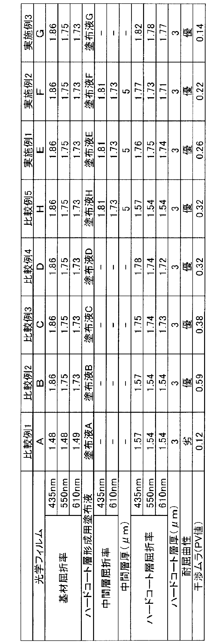
- composition for forming hard coat layer Each component was put into a mixing tank with the composition (parts by mass) shown in Table 1 below, stirred, and filtered through a polypropylene filter having a pore size of 0.4 ⁇ m to prepare coating solutions A to H.
- DPHA Mixture of dipentaerythritol pentaacrylate and dipentaerythritol hexaacrylate (manufactured by Nippon Kayaku Co., Ltd.)
- PET30 A mixture of pentaerythritol tetraacrylate and pentaerythritol triacrylate (manufactured by Nippon Kayaku Co., Ltd.)
- OGSOL EA-0200 Acrylate monomer having a fluorene skeleton (Osaka Gas Chemical Co., Ltd.) Zirconia particles (30% toluene solution): average primary particle size 20 nm (manufactured by CIK Nanotech Co., Ltd.)
- Irgacure 184 Photopolymerization initiator (manufactured by BASF)
- the coating liquid A was apply
- Coating solutions B to H were each coated on the substrate S-4 using a gravure coater. After drying at 120 ° C., an ultraviolet ray with an irradiation amount of 300 mJ / cm 2 using a 160 W / cm air-cooled metal halide lamp (made by Eye Graphics Co., Ltd.) while purging with nitrogen so that the oxygen concentration becomes 100 ppm or less. Were applied to cure the coating layer to form a hard coat layer, and optical films B to H were produced. The coating amount was adjusted so that the thickness of the hard coat layer was 3 ⁇ m.
- a portion of the polymer solution obtained above is cast on an endless belt at 120 ° C. using a T-die so that the final film thickness is 40 ⁇ m, and dried so that the polymer concentration is 40% by mass. Peeled from the endless belt.
- the film containing the solvent was stretched 1.1 times in the MD (Machine Direction) direction in the atmosphere at 40 ° C., and washed with water at 50 ° C. to remove the solvent. Furthermore, it was stretched 1.2 times in the TD (Transverse Direction) direction in a drying furnace at 340 ° C. to obtain a substrate S-4 made of aromatic polyamide and having a thickness of 40 ⁇ m.
- an optical film having excellent bending resistance and suppressing occurrence of interference unevenness it is possible to provide an optical film having excellent bending resistance and suppressing occurrence of interference unevenness, a polarizing plate having the optical film, and an image display device.
Landscapes
- Physics & Mathematics (AREA)
- General Physics & Mathematics (AREA)
- Optics & Photonics (AREA)
- Nonlinear Science (AREA)
- Mathematical Physics (AREA)
- Chemical & Material Sciences (AREA)
- Crystallography & Structural Chemistry (AREA)
- Surface Treatment Of Optical Elements (AREA)
- Polarising Elements (AREA)
- Laminated Bodies (AREA)
- Liquid Crystal (AREA)
Abstract
Description
基材上にハードコート層を有する光学フィルムは、基材とハードコート層との界面による反射光と、ハードコート層表面からの反射光の干渉により色味がついた干渉ムラが発生することがある。干渉ムラは、画像表示装置の表示画像の視認性や画像品位を損なうため、その改善が求められている。
たとえば、特許文献1には、セルロースアシレートを含有する基材に対する溶解能を有する溶媒を用いて、ハードコート層から基材にかけて屈折率が緩やかに変化したグラデーション層を設けることで干渉ムラを抑制する技術が開示されている。
また、特許文献3には、特定のアクリル系樹脂と特定の脂肪族ポリアミドとを用いることにより、耐屈曲性を付与した光学フィルムが記載されている。
特許文献5には、フルオレン骨格を有するモノマーを含有するハードコート性樹脂組成物が記載されている。
更に、特許文献4に記載されているように、アンカーコート層に金属酸化物粒子を含有させることによりアンカーコート層とプラスチック基材の屈折率差を小さくして、その界面での反射を少なくして色むらを減少する技術、及び特許文献5に記載されているように、フルオレン骨格を有するモノマーを含むハードコート性樹脂組成物を用いることにより、屈折率の高い硬化物を得る技術は知られているが、アラミドを含有する基材は短波長における屈折率が非常に高く、単にこれらの技術を適用したのみでは干渉ムラは抑制できないことが分かった。
基材とハードコート層とを有する光学フィルムであって、
上記基材の波長550nmにおける屈折率が1.60以上であり、
上記基材の波長435nmにおける屈折率と波長610nmにおける屈折率との差が0.11以上であり、
上記光学フィルムの反射率スペクトルを高速フーリエ変換して得られたパワースペクトルのピーク強度PV値が0.3以下である、光学フィルム。
<2>
上記基材と上記ハードコート層との間に、更に中間層を有し、
上記ハードコート層が無機粒子を含有し、
波長435nmにおける上記基材の屈折率と波長435nmにおける上記中間層の屈折率との差が0.05以下であり、
波長435nmにおける上記中間層の屈折率と波長435nmにおける上記ハードコート層の屈折率との差が0.05以下であり、
波長610nmにおける上記基材の屈折率と波長610nmにおける上記中間層の屈折率との差が0.05以下であり、
波長610nmにおける上記中間層の屈折率と波長610nmにおける上記ハードコート層の屈折率との差が0.05以下である、<1>に記載の光学フィルム。
<3>
上記基材と上記ハードコート層との間に、更に中間層を有し、
上記ハードコート層がフルオレン骨格、ジナフトチオフェン骨格、ナフタレン骨格、アントラセン骨格、ベンゾトリアゾール骨格、トリアジン骨格、ベンゾフェノン骨格、メロシアニン骨格、ベンゾオキサゾール骨格、ベンゾチオール骨格、トリフェニレン骨格、シンナモイル骨格、ビスフェノールS骨格、及びトラン骨格から選ばれる少なくとも1種の骨格を有するモノマーの重合体を含有し、
波長435nmにおける上記基材の屈折率と波長435nmにおける上記中間層の屈折率との差が0.05以下であり、
波長435nmにおける上記中間層の屈折率と波長435nmにおける上記ハードコート層の屈折率との差が0.05以下であり、
波長610nmにおける上記基材の屈折率と波長610nmにおける上記中間層の屈折率との差が0.05以下であり、
波長610nmにおける上記中間層の屈折率と波長610nmにおける上記ハードコート層の屈折率との差が0.05以下である、<1>に記載の光学フィルム。
<4>
上記基材と上記ハードコート層とが接しており、
上記ハードコート層が、無機粒子と、フルオレン骨格、ジナフトチオフェン骨格、ナフタレン骨格、アントラセン骨格、ベンゾトリアゾール骨格、トリアジン骨格、ベンゾフェノン骨格、メロシアニン骨格、ベンゾオキサゾール骨格、ベンゾチオール骨格、トリフェニレン骨格、シンナモイル骨格、ビスフェノールS骨格、及びトラン骨格から選ばれる少なくとも1種の骨格を有するモノマーの重合体とを含有し、
波長435nmにおける上記基材の屈折率と波長435nmにおける上記ハードコート層の屈折率との差が0.05以下であり、
波長610nmにおける上記基材の屈折率と波長610nmにおける上記ハードコート層の屈折率との差が0.05以下である、<1>に記載の光学フィルム。
<5>
上記基材がアラミドを含有する、<1>~<4>のいずれか1項に記載の光学フィルム。
<6>
上記ハードコート層の波長550nmにおける屈折率が1.56以上である、<1>~<5>のいずれか1項に記載の光学フィルム。
<7>
上記光学フィルムが、JIS P8115(2001)に従いMIT試験機によって測定した耐折回数が1000回以上である、<1>~<6>のいずれか1項に記載の光学フィルム。
<8>
<1>~<7>のいずれか1項に記載の光学フィルムを有する偏光板。
<9>
<1>~<7>のいずれか1項に記載の光学フィルム又は<8>に記載の偏光板を有する画像表示装置。
なお、本発明においては、「モノマーに相当する繰り返し単位」、及び「モノマーに由来する繰り返し単位」とは、モノマーの重合後に得られる成分が繰り返し単位となることを意味している。
本発明の光学フィルムは、
基材とハードコート層とを有する光学フィルムであって、
基材の波長550nmにおける屈折率が1.60以上であり、
基材の波長435nmにおける屈折率と波長610nmにおける屈折率との差(基材の波長435nmにおける屈折率-基材の波長610nmにおける屈折率)が0.11以上であり、
光学フィルムの反射率スペクトルを高速フーリエ変換して得られたパワースペクトルのピーク強度PV値が0.3以下である、光学フィルムである。
本発明の光学フィルムは、反射率スペクトルをフーリエ変換して得られたパワースペクトルのピーク強度PV値(単に「PV値」とも呼ぶ。)が0.3以下である。
PV値とは界面の反射の大きさを表す値で、反射率スペクトルの薄膜干渉由来の変動を高速フーリエ変換して得たパワースペクトルのピーク強度をいう。界面での屈折率差が小さければ強度は小さく、屈折率差が大きくなれば強度は大きくなる。
光学フィルムが中間層を有する場合には、上記パワースペクトルにおける基材と中間層及び中間層とハードコート層との2つの界面に対応するピーク強度のうち値の大きい方をPV値として、干渉ムラの指標とする。この値が小さいほど干渉ムラがより抑制されたことを意味する。
基材とハードコート層との間に、更に中間層を有し、
ハードコート層が無機粒子を含有し、
波長435nmにおける基材の屈折率と波長435nmにおける中間層の屈折率との差が0.05以下であり、
波長435nmにおける中間層の屈折率と波長435nmにおけるハードコート層の屈折率との差が0.05以下であり、
波長610nmにおける基材の屈折率と波長610nmにおける中間層の屈折率との差が0.05以下であり、
波長610nmにおける中間層の屈折率と波長610nmにおけるハードコート層の屈折率との差が0.05以下である態様。
基材とハードコート層との間に、更に中間層を有し、
ハードコート層がフルオレン骨格、ジナフトチオフェン骨格、ナフタレン骨格、アントラセン骨格、ベンゾトリアゾール骨格、トリアジン骨格、ベンゾフェノン骨格、メロシアニン骨格、ベンゾオキサゾール骨格、ベンゾチオール骨格、トリフェニレン骨格、シンナモイル骨格、ビスフェノールS骨格、及びトラン骨格から選ばれる少なくとも1種の骨格を有するモノマーの重合体を含有し、
波長435nmにおける基材の屈折率と波長435nmにおける中間層の屈折率との差が0.05以下であり、
波長435nmにおける中間層の屈折率と波長435nmにおけるハードコート層の屈折率との差が0.05以下であり、
波長610nmにおける基材の屈折率と波長610nmにおける中間層の屈折率との差が0.05以下であり、
波長610nmにおける中間層の屈折率と波長610nmにおけるハードコート層の屈折率との差が0.05以下である態様。
基材とハードコート層とが接しており、
ハードコート層が、無機粒子と、フルオレン骨格、ジナフトチオフェン骨格、ナフタレン骨格、アントラセン骨格、ベンゾトリアゾール骨格、トリアジン骨格、ベンゾフェノン骨格、メロシアニン骨格、ベンゾオキサゾール骨格、ベンゾチオール骨格、トリフェニレン骨格、シンナモイル骨格、ビスフェノールS骨格、及びトラン骨格から選ばれる少なくとも1種の骨格を有するモノマーの重合体とを含有し、
波長435nmにおける基材の屈折率と波長435nmにおけるハードコート層の屈折率との差が0.05以下であり、
波長610nmにおける基材の屈折率と波長610nmにおけるハードコート層の屈折率との差が0.05以下である態様。
上記態様(A)及び(B)において、
波長435nmにおける基材の屈折率と波長435nmにおける中間層の屈折率との差は0.03以下であることが好ましく、
波長435nmにおける中間層の屈折率と波長435nmにおけるハードコート層の屈折率との差は0.03以下であることが好ましく、
波長610nmにおける基材の屈折率と波長610nmにおける中間層の屈折率との差は0.03以下であることが好ましく、
波長610nmにおける中間層の屈折率と波長610nmにおけるハードコート層の屈折率との差は0.03以下であることが好ましい。
上記態様(C)において、
波長435nmにおける基材の屈折率と波長435nmにおけるハードコート層の屈折率との差は0.03以下であることが好ましく、
波長610nmにおける基材の屈折率と波長610nmにおけるハードコート層の屈折率との差は0.03以下であることが好ましい。
本発明の光学フィルムの基材は、波長550nmにおける屈折率が1.60以上であり、波長435nmにおける屈折率と波長610nmにおける屈折率との差が0.11以上である。
基材は、可視光領域の透過率が70%以上であることが好ましく、80%以上であることがより好ましい。
基材としては、アラミドを含有する基材であることが好ましい。
基材の厚みは特に限定されないが、3μm~100μmが好ましく、5μm~80μmがより好ましく、15μm~50μmが更に好ましい。
前述の態様(A)及び(B)の場合のハードコート層の屈折率について以下に説明する。
ハードコート層の波長550nmにおける屈折率は1.56以上であることが好ましく、1.63以上1.79以下であることが好ましく、1.66以上1.76以下であることがより更に好ましい。ハードコート層の波長550nmにおける屈折率は1.56以上であると、基材との屈折率差が小さくなり、干渉ムラの発生が抑制されやすい。
ハードコート層の波長435nmにおける屈折率は、1.73以上1.89以下であることが好ましく、1.76以上1.86以下であることがより好ましい。
ハードコート層の波長610nmにおける屈折率は、1.60以上1.76以下であることが好ましく、1.63以上1.73以下であることがより好ましい。
ハードコート層の波長550nmにおける屈折率は1.56以上であることが好ましく、1.68以上1.84以下であることが好ましく、1.71以上1.81以下であることがより更に好ましい。ハードコート層の波長550nmにおける屈折率は1.56以上であると、基材との屈折率差が小さくなり、干渉ムラの発生が抑制されやすい。
ハードコート層の波長435nmにおける屈折率は、1.78以上1.93以下であることが好ましく、1.81以上1.91以下であることがより好ましい。
ハードコート層の波長610nmにおける屈折率は、1.65以上1.81以下であることが好ましく、1.68以上1.78以下であることがより好ましい。
前述の態様(A)及び(C)においては、ハードコート層は無機粒子を含有する。なお、前述の態様(B)においてもハードコート層が更に無機粒子を含有してもよい。
無機粒子としては、金属(たとえば、Ti、Zr、In、Zn、Sn、Sb、及びAlなど)の酸化物の粒子であることが好ましく、屈折率の観点から、酸化ジルコニウム粒子又は酸化チタン粒子であることがより好ましく、酸化チタン粒子を平均1次粒径10nm未満にすると光活性が強まり、周囲の有機物を分解し易くなり得る観点から、酸化ジルコニウム粒子(ジルコニア粒子)が最も好ましい。
ハードコート層中の無機粒子の含有率を変化させることで屈折率を調整することができる。
ハードコート層中の無機粒子の含有率は、ハードコート層全体に対して、5~80体積%であることが好ましく、10~60体積%であることがより好ましく、20~50体積%であることが更に好ましい。無機粒子の含有率が5体積%以上であれば、ハードコート層の屈折率を高くすることができ、80体積%以下であれば膜を形成しやすい。
ハードコート層中の無機粒子の、質量%に換算したときの好適含有率は、無機粒子の比重によって変わり、例えば無機粒子として比重6の酸化ジルコニウム粒子を用いる場合の含有率は、ハードコート層全体に対して、21~95質量%であることが好ましく、36~88質量%であることがより好ましく、56~83質量%であることが更に好ましい。
無機粒子の平均1次粒径は、1~80nmであることが好ましく、1~40nmであることがより好ましく、2~20nmであることが更に好ましい。
また、無機粒子は後述する樹脂をバインダー成分としてハードコート層中に含有されることが好ましく、ハードコート層中のバインダー成分との密着性を向上させるために、重合性基を有する化合物で修飾して、無機粒子の表面に重合性基を付与することが好ましい。
前述の態様(A)~(C)において、ハードコート層は樹脂を含有することが好ましく、上記樹脂はモノマー(重合性化合物)の重合体であることが好ましい。
モノマーは1種でも2種以上を併用してもよい。
モノマーは(メタ)アクリロイル基、ビニル基、スチリル基、アリル基等の不飽和の重合性官能基を有することが好ましく、中でも、(メタ)アクリロイル基を有することが好ましい。
前述の態様(B)及び(C)においては、上記モノマーとして、フルオレン骨格、ジナフトチオフェン骨格、ナフタレン骨格、アントラセン骨格、ベンゾトリアゾール骨格、トリアジン骨格、ベンゾフェノン骨格、メロシアニン骨格、ベンゾオキサゾール骨格、ベンゾチオール骨格、トリフェニレン骨格、シンナモイル骨格、ビスフェノールS骨格、及びトラン骨格から選ばれる少なくとも1種の骨格を有する化合物(「モノマー(a)」とも呼ぶ。)を含むことが好ましい。
モノマー(a)を用いることで、ハードコート層の屈折率を高くすることができる。モノマー(a)の具体例としては、特開2007-91876号公報の段落0029~0046に記載の一般式(I)~(VI)で表される化合物、特開2014-34596号公報の段落0113~0115に記載のフルオレン化合物、特開2014-80572号公報の一般式(1)で表される縮合環含有化合物(好ましくは同公報の一般式(3)で表される縮合環含有化合物)、特開2013-253161号公報の段落0016に記載の化合物、特開2006-301614号公報の段落0025~0153に記載の化合物、特開2007-108732号公報の段落0020~0122に記載の化合物、特開2010-244038号公報の段落0012~0108に記載の化合物等が挙げられる。
モノマー(a)としては、特に、フルオレン骨格、ジナフトチオフェン骨格、ナフタレン骨格、及びアントラセン骨格から選ばれる少なくとも1種の骨格を有する化合物が好ましく、フルオレン骨格を有する化合物が最も好ましい。
なお、前述の態様(A)においてもハードコート層が更にモノマー(a)を含むモノマーの重合体を含有してもよい。
前述の態様(A)及び(B)においては、ハードコート層の樹脂を形成するためのモノマーとして、上記モノマー(a)以外のモノマー(「モノマー(b)」とも呼ぶ。)を用いることも好ましい。このようなモノマーの具体例としては、ネオペンチルグリコールアクリレート、1,6-ヘキサンジオール(メタ)アクリレート、プロピレングリコールジ(メタ)アクリレート等のアルキレングリコールの(メタ)アクリル酸ジエステル類;
トリエチレングリコールジ(メタ)アクリレート、ジプロピレングリコールジ(メタ)アクリレート、ポリエチレングリコールジ(メタ)アクリレート、ポリプロピレングリコールジ(メタ)アクリレート等のポリオキシアルキレングリコールの(メタ)アクリル酸ジエステル類;
ペンタエリスリトールジ(メタ)アクリレート等の多価アルコールの(メタ)アクリル酸ジエステル類;
2,2-ビス{4-(アクリロキシ・ジエトキシ)フェニル}プロパン、2-2-ビス{4-(アクリロキシ・ポリプロポキシ)フェニル}プロパン等のエチレンオキシドあるいはプロピレンオキシド付加物の(メタ)アクリル酸ジエステル類;等を挙げることができる。
例えば、ペンタエリスリトールテトラ(メタ)アクリレート、ペンタエリスリトールトリ(メタ)アクリレート、トリメチロールプロパントリ(メタ)アクリレート、エチレンオキサイド(EO)変性トリメチロールプロパントリ(メタ)アクリレート、プロピレンオキサイド(PO)変性トリメチロールプロパントリ(メタ)アクリレート、EO変性リン酸トリ(メタ)アクリレート、トリメチロールエタントリ(メタ)アクリレート、ジトリメチロールプロパンテトラ(メタ)アクリレート、ジペンタエリスリトールテトラ(メタ)アクリレート、ジペンタエリスリトールペンタ(メタ)アクリレート、ジペンタエリスリトールヘキサ(メタ)アクリレート、ペンタエリスリトールヘキサ(メタ)アクリレート、1,2,3-クロヘキサンテトラメタクリレート、ポリウレタンポリアクリレート、ポリエステルポリアクリレート、カプロラクトン変性トリス(アクリロキシエチル)イソシアヌレート等が挙げられる。
なお、前述の態様(C)においてもハードコート層の樹脂を形成するためのモノマーとして、モノマー(b)を併用してもよい。
上記態様(A)及び(B)の中間層について説明する。
中間層は、波長435nmにおける屈折率及び波長610nmにおける屈折率が前述の関係を満たすものであれば特に限定されないが、基材中の成分(好ましくはアラミド)とハードコート層中の成分(上記態様(A)では好ましくはモノマーの重合体、上記態様(B)では好ましくはモノマー(a)を含むモノマーの重合体)の両方を含有する層であることが好ましい。
中間層の膜厚は特に限定されないが、1μm~10μmであることが好ましく、3μm~8μmであることがより好ましく、5μm~7μmであることが更に好ましい。
ハードコート層及び中間層の膜厚は以下のようにして求める。
接触式厚み計でハードコート層形成前の基材の厚みと、作製した光学フィルム試料の厚みを測定する。また、光学フィルム試料をミクロトームで切削して断面を出し、光学顕微鏡で観察してハードコート層の膜厚を算出する。
中間層の膜厚は下記式により算出される。
(中間層の膜厚)=(光学フィルム試料の厚み)-(ハードコート層形成前の基材の厚み)-(ハードコート層の膜厚)
光学フィルムのハードコート層を設けていない側の面に黒色に塗り潰したポリエチレンテレフタレートフィルムを貼合して測定試料を作成する。測定試料を反射分光膜厚計(大塚電子(株)製 商品名 FE-3000)にセットし、D2ランプ光源を用いて、反射スペクトルを求める。付属のソフトで基板解析を行い、350~800nmの波長範囲をn-Cauchyで演算を行い、屈折率を算出する。ハードコート層の屈折率は、光学フィルム表面の測定を行い、中間層の屈折率は、光学フィルムの膜厚方向の切断面をミクロトームにて斜め切削して、中間層部分の測定を行う。基材の屈折率はハードコート層形成前の基材又は斜め切削により基材部分の測定を行ってもよい。
上記態様(A)の光学フィルムは、基材上に、無機粒子とモノマーと基材を膨潤させる溶剤とを含有するハードコート層形成用組成物を塗布する工程、及びモノマーを重合させる工程を含む光学フィルムの製造方法により製造されることが好ましい。
上記態様(B)の光学フィルムは、基材上に、モノマー(a)を含むモノマーと基材を膨潤させる溶剤とを含有するハードコート層形成用組成物を塗布する工程、及びモノマーを重合させる工程を含む光学フィルムの製造方法により製造されることが好ましい。
上記態様(C)の光学フィルムは、基材上に、無機粒子とモノマー(a)を含むモノマーと溶剤とを含有するハードコート層形成用組成物を塗布する工程、及びモノマーを重合させる工程を含む光学フィルムの製造方法により製造されることが好ましい。
基材を膨潤させる溶剤としては、沸点が180℃以下の溶剤が好ましく、例えば、酢酸メチル、酢酸エチル、メチルイソブチルケトン、メチルエチルケトン、アセトン、エタノール、メタノール、1-メトキシ-2-プロパノール、及びシクロヘキサノンが挙げられる。
基材を膨潤させる溶剤とは、25℃の溶剤に5cm角の基材を5分間浸漬し、次いで120℃で5分間乾燥した後、基材を平らな面に置いた場合に、その投影図が4.5cm角の枠内に収まらない溶剤、及び/又は、基材の質量が元の質量の99.0%以下となる溶剤である。
また、上記態様(A)及び(B)の光学フィルムを製造する場合には、基材を膨潤させる溶剤に加えて、上記溶剤を用いてもよい。
ハードコート層形成用組成物は、重合開始剤を含んでいてもよい。
モノマーが光重合性化合物である場合は、光重合開始剤を含むことが好ましい。
光重合開始剤としては、アセトフェノン類、ベンゾイン類、ベンゾフェノン類、ホスフィンオキシド類、ケタール類、アントラキノン類、チオキサントン類、アゾ化合物、過酸化物類、2,3-ジアルキルジオン化合物類、ジスルフィド化合物類、フルオロアミン化合物類、芳香族スルホニウム類、ロフィンダイマー類、オニウム塩類、ボレート塩類、活性エステル類、活性ハロゲン類、無機錯体、クマリン類などが挙げられる。光重合開始剤の具体例、及び好ましい態様、市販品などは、特開2009-098658号公報の段落[0133]~[0151]に記載されており、本発明においても同様に好適に用いることができる。
「最新UV硬化技術」{(株)技術情報協会}(1991年)、p.159、及び、「紫外線硬化システム」加藤清視著(平成元年、総合技術センター発行)、p.65~148にも種々の例が記載されており本発明に有用である。
ハードコート層形成用組成物中の重合開始剤の含有率は、ハードコート層形成用組成物中の全固形分に対して、0.5~8質量%が好ましく、1~5質量%がより好ましい。
本発明の光学フィルムを用いた偏光板保護フィルムは、偏光子と貼り合せて偏光板とすることができ、液晶表示装置などに好適に用いることができる。
偏光板は、偏光子と、偏光子を保護する少なくとも1枚の保護フィルムとを有する偏光板であって、保護フィルムの少なくとも1枚が本発明の光学フィルムであることが好ましい。
本発明の光学フィルム又は偏光板を画像表示装置に適用することもできる。
画像表示装置としては、陰極線管(CRT)を利用した表示装置、プラズマディスプレイパネル(PDP)、エレクトロルミネッセンスディスプレイ(ELD)、蛍光表示ディスプレイ(VFD)、フィールドエミッションディスプレイ(FED)、及び液晶ディスプレイ(LCD)を挙げることができ、特に液晶表示装置が好ましい。
一般的に、液晶表示装置は、液晶セル及びその両側に配置された2枚の偏光板を有し、液晶セルは、2枚の電極基板の間に液晶を担持している。更に、光学異方性層が、液晶セルと一方の偏光板との間に一枚配置されるか、又は液晶セルと双方の偏光板との間に2枚配置されることもある。液晶セルは、TN(Twisted Nematic)モード、VA(Vertically Aligned)モード、OCB(Optically Compensatory Bend)モード、IPS(In-Plane Switching)モードなど様々な駆動方式の液晶セルが適用できる。
下記に示す通りに、ハードコート層形成用組成物(塗布液)を調製し、それぞれのハードコート層形成用組成物を用いてハードコート層を形成して、光学フィルム試料を作製した。
下記表1に記載の組成(質量部)で各成分をミキシングタンクに投入し、攪拌して、孔径0.4μmのポリプロピレン製フィルターで濾過して塗布液A~Hを調製した。

PET30:ペンタエリスリトールテトラアクリレートとペンタエリスリトールトリアクリレートの混合物(日本化薬(株)製)
OGSOL EA-0200:フルオレン骨格を有するアクリレートモノマー(大阪ガスケミカル(株)製)
ジルコニア粒子(トルエン30%溶液):平均1次粒径20nm(CIKナノテック(株)製)
イルガキュア184:光重合開始剤(BASF製)
厚さ40μmの基材としてのトリアセチルセルロースフィルム(フジタック TD40UL、富士フイルム(株)製)上に、塗布液Aをグラビアコーターを用いて塗布した。100℃で乾燥した後、酸素濃度が100ppm以下の雰囲気になるように窒素パージしながら160W/cmの空冷メタルハライドランプ(アイグラフィックス(株)製)を用いて、照射量300mJ/cm2の紫外線を照射して塗布層を硬化させ、ハードコート層を形成し、光学フィルムAを作製した。ハードコート層の厚みは3μmとなるように塗布量を調整した。
基材S-4上に、塗布液B~Hをそれぞれグラビアコーターを用いて塗布した。120℃で乾燥した後、酸素濃度が100ppm以下の雰囲気になるように窒素パージしながら160W/cmの空冷メタルハライドランプ(アイグラフィックス(株)製)を用いて、照射量300mJ/cm2の紫外線を照射して塗布層を硬化させ、ハードコート層を形成し、光学フィルムB~Hを作製した。ハードコート層の厚みは3μmとなるように塗布量を調整した。
[芳香族ポリアミドの合成]
攪拌機を備えた重合槽にN-メチル-2-ピロリドン674.7kg、無水臭化リチウム10.6g(シグマアルドリッチジャパン社製)、2,2’-ジトリフルオロメチル-4,4’-ジアミノビフェニル(東レファインケミカル社製「TFMB」)33.3g、4,4’-ジアミノジフェニルスルフォン(和歌山精化株式会社製「44DDS」)2.9gを入れ窒素雰囲気下、15℃に冷却、攪拌しながら300分かけてテレフタル酸ジクロライド(東京化成社製)18.5g、4,4’-ビフェニルジカルボニルクロライド(東レファインケミカル社製「4BPAC」)6.4gを4回に分けて添加した。60分間攪拌した後、反応で発生した塩化水素を炭酸リチウムで中和してポリマー溶液を得た。
光学フィルムのハードコート層を設けていない側の面に黒色に塗り潰したポリエチレンテレフタレートフィルムを貼合して測定試料を作成した。測定試料を反射分光膜厚計(大塚電子(株)製 商品名 FE-3000)にセットし、D2ランプ光源を用いて、反射スペクトルを求めた。得られたスペクトルを高速フーリエ解析し、干渉ムラに由来するピーク強度PV値を求めた。また、複数のPV値を保つ場合は、最も大きいものをPV値として採用した。
材料カテゴリ : Standard
アルゴリズム : FFT(Fast Fourier Transform)
FFT解析 演算波長範囲 : 400.00~750.00nm
耐折度試験機(テスター産業(株)製、MIT、BE-201型、折り曲げ曲率半径0.38mm)を用いて、温度25℃、相対湿度65%の状態に1時間以上静置させた、幅15mm、長さ150mmの試料フィルムを使用し、荷重500gの条件で、JIS P8115(2001)に準拠して測定し、破断するまでの回数で評価した。破断するまでの回数が多いほど耐屈曲性に優れていることを表し、繰り返しの折り曲げ耐性に優れていることを表す。
破断するまでの回数が1000回未満のものを「劣」とし、1000回以上のものを「優」とした。
本出願は、2016年3月25日出願の日本特許出願(特願2016-062131)に基づくものであり、その内容はここに参照として取り込まれる。
Claims (9)
- 基材とハードコート層とを有する光学フィルムであって、
前記基材の波長550nmにおける屈折率が1.60以上であり、
前記基材の波長435nmにおける屈折率と波長610nmにおける屈折率との差が0.11以上であり、
前記光学フィルムの反射率スペクトルを高速フーリエ変換して得られたパワースペクトルのピーク強度PV値が0.3以下である、光学フィルム。 - 前記基材と前記ハードコート層との間に、更に中間層を有し、
前記ハードコート層が無機粒子を含有し、
波長435nmにおける前記基材の屈折率と波長435nmにおける前記中間層の屈折率との差が0.05以下であり、
波長435nmにおける前記中間層の屈折率と波長435nmにおける前記ハードコート層の屈折率との差が0.05以下であり、
波長610nmにおける前記基材の屈折率と波長610nmにおける前記中間層の屈折率との差が0.05以下であり、
波長610nmにおける前記中間層の屈折率と波長610nmにおける前記ハードコート層の屈折率との差が0.05以下である、請求項1に記載の光学フィルム。 - 前記基材と前記ハードコート層との間に、更に中間層を有し、
前記ハードコート層がフルオレン骨格、ジナフトチオフェン骨格、ナフタレン骨格、アントラセン骨格、ベンゾトリアゾール骨格、トリアジン骨格、ベンゾフェノン骨格、メロシアニン骨格、ベンゾオキサゾール骨格、ベンゾチオール骨格、トリフェニレン骨格、シンナモイル骨格、ビスフェノールS骨格、及びトラン骨格から選ばれる少なくとも1種の骨格を有するモノマーの重合体を含有し、
波長435nmにおける前記基材の屈折率と波長435nmにおける前記中間層の屈折率との差が0.05以下であり、
波長435nmにおける前記中間層の屈折率と波長435nmにおける前記ハードコート層の屈折率との差が0.05以下であり、
波長610nmにおける前記基材の屈折率と波長610nmにおける前記中間層の屈折率との差が0.05以下であり、
波長610nmにおける前記中間層の屈折率と波長610nmにおける前記ハードコート層の屈折率との差が0.05以下である、請求項1に記載の光学フィルム。 - 前記基材と前記ハードコート層とが接しており、
前記ハードコート層が、無機粒子と、フルオレン骨格、ジナフトチオフェン骨格、ナフタレン骨格、アントラセン骨格、ベンゾトリアゾール骨格、トリアジン骨格、ベンゾフェノン骨格、メロシアニン骨格、ベンゾオキサゾール骨格、ベンゾチオール骨格、トリフェニレン骨格、シンナモイル骨格、ビスフェノールS骨格、及びトラン骨格から選ばれる少なくとも1種の骨格を有するモノマーの重合体とを含有し、
波長435nmにおける前記基材の屈折率と波長435nmにおける前記ハードコート層の屈折率との差が0.05以下であり、
波長610nmにおける前記基材の屈折率と波長610nmにおける前記ハードコート層の屈折率との差が0.05以下である、請求項1に記載の光学フィルム。 - 前記基材がアラミドを含有する、請求項1~4のいずれか1項に記載の光学フィルム。
- 前記ハードコート層の波長550nmにおける屈折率が1.56以上である、請求項1~5のいずれか1項に記載の光学フィルム。
- 前記光学フィルムが、JIS P8115(2001)に従いMIT試験機によって測定した耐折回数が1000回以上である、請求項1~6のいずれか1項に記載の光学フィルム。
- 請求項1~7のいずれか1項に記載の光学フィルムを有する偏光板。
- 請求項1~7のいずれか1項に記載の光学フィルム又は請求項8に記載の偏光板を有する画像表示装置。
Priority Applications (2)
| Application Number | Priority Date | Filing Date | Title |
|---|---|---|---|
| KR1020187026377A KR102178543B1 (ko) | 2016-03-25 | 2017-03-17 | 광학 필름, 편광판, 및 화상 표시 장치 |
| US16/130,327 US11644604B2 (en) | 2016-03-25 | 2018-09-13 | Optical film, polarizing plate, and image display device |
Applications Claiming Priority (2)
| Application Number | Priority Date | Filing Date | Title |
|---|---|---|---|
| JP2016062131A JP6574731B2 (ja) | 2016-03-25 | 2016-03-25 | 光学フィルム、偏光板、及び画像表示装置 |
| JP2016-062131 | 2016-03-25 |
Related Child Applications (1)
| Application Number | Title | Priority Date | Filing Date |
|---|---|---|---|
| US16/130,327 Continuation US11644604B2 (en) | 2016-03-25 | 2018-09-13 | Optical film, polarizing plate, and image display device |
Publications (1)
| Publication Number | Publication Date |
|---|---|
| WO2017164137A1 true WO2017164137A1 (ja) | 2017-09-28 |
Family
ID=59899465
Family Applications (1)
| Application Number | Title | Priority Date | Filing Date |
|---|---|---|---|
| PCT/JP2017/011053 Ceased WO2017164137A1 (ja) | 2016-03-25 | 2017-03-17 | 光学フィルム、偏光板、及び画像表示装置 |
Country Status (4)
| Country | Link |
|---|---|
| US (1) | US11644604B2 (ja) |
| JP (1) | JP6574731B2 (ja) |
| KR (1) | KR102178543B1 (ja) |
| WO (1) | WO2017164137A1 (ja) |
Cited By (2)
| Publication number | Priority date | Publication date | Assignee | Title |
|---|---|---|---|---|
| KR102025321B1 (ko) * | 2018-10-02 | 2019-09-25 | 스미또모 가가꾸 가부시키가이샤 | 광학 필름, 플렉시블 표시 장치 및 광학 필름의 제조 방법 |
| KR102028037B1 (ko) * | 2018-10-02 | 2019-10-02 | 스미또모 가가꾸 가부시키가이샤 | 광학 필름, 플렉시블 표시 장치 및 광학 필름의 제조 방법 |
Families Citing this family (1)
| Publication number | Priority date | Publication date | Assignee | Title |
|---|---|---|---|---|
| CN115461659B (zh) * | 2020-04-30 | 2025-07-18 | 日东电工株式会社 | 偏光板及使用该偏光板的图像显示装置 |
Citations (11)
| Publication number | Priority date | Publication date | Assignee | Title |
|---|---|---|---|---|
| JPH11133206A (ja) * | 1997-10-24 | 1999-05-21 | Sony Corp | 反射防止フィルタおよびこの反射防止フィルタを用いた文字画像表示装置 |
| WO2005105918A1 (ja) * | 2004-04-28 | 2005-11-10 | Toray Industries, Inc. | アクリル樹脂フィルムおよび製造方法 |
| JP2006051668A (ja) * | 2004-08-11 | 2006-02-23 | Toray Ind Inc | 芳香族ポリアミドフィルムおよびそれを用いた光学部材およびディスプレイ。 |
| JP2009133880A (ja) * | 2006-03-10 | 2009-06-18 | Toyo Ink Mfg Co Ltd | 樹脂組成物 |
| JP2010044128A (ja) * | 2008-08-11 | 2010-02-25 | Toray Advanced Film Co Ltd | ディスプレイ用フィルター |
| JP2015052790A (ja) * | 2009-12-28 | 2015-03-19 | 大日本印刷株式会社 | 光学フィルム、光学フィルムの製造方法、偏光板、ディスプレイパネル及びディスプレイ |
| JP2015106033A (ja) * | 2013-11-29 | 2015-06-08 | 凸版印刷株式会社 | 光学フィルム |
| JP2015143754A (ja) * | 2014-01-31 | 2015-08-06 | 富士フイルム株式会社 | 透明フィルム及びその製造方法、透明導電フィルム、タッチパネル、反射防止フィルム、偏光板および表示装置 |
| JP2015188772A (ja) * | 2014-03-27 | 2015-11-02 | 大日本印刷株式会社 | 光学積層体及びその製造方法 |
| JP2016022684A (ja) * | 2014-07-22 | 2016-02-08 | Jsr株式会社 | 積層体 |
| JP2017033033A (ja) * | 2015-07-17 | 2017-02-09 | 大日本印刷株式会社 | タッチパネル用積層体、折り畳み式画像表示装置 |
Family Cites Families (11)
| Publication number | Priority date | Publication date | Assignee | Title |
|---|---|---|---|---|
| ITSV20030018A1 (it) * | 2003-04-11 | 2004-10-12 | Allaix Roberto C O Ferrania S P A Uff Brevetti | Mezzo ottico comprendente un film di materiale polimerico. |
| ITSV20030019A1 (it) * | 2003-04-11 | 2004-10-12 | Allaix Roberto C O Ferrania S P A Uff Brevetti | Film ottici comprendenti uno o piu' poliarilati ottenuti |
| JP5685074B2 (ja) | 2009-12-28 | 2015-03-18 | 大日本印刷株式会社 | 光学フィルム、光学フィルムの製造方法、偏光板、ディスプレイパネル及びディスプレイ |
| JP2012078541A (ja) | 2010-09-30 | 2012-04-19 | Fujifilm Corp | 光学フィルム、偏光板、画像表示装置、及び光学フィルムの製造方法 |
| EP2636697B1 (en) * | 2010-11-01 | 2018-08-15 | Nissan Chemical Industries, Ltd. | Triazine ring-containing polymer and film-forming composition containing same |
| JP5779039B2 (ja) | 2010-11-01 | 2015-09-16 | 大阪ガスケミカル株式会社 | ハードコート性樹脂組成物及びその硬化物 |
| JP2013091290A (ja) | 2011-10-27 | 2013-05-16 | Toppan Printing Co Ltd | 透明ガスバリア積層体 |
| JP6010992B2 (ja) * | 2012-04-11 | 2016-10-19 | 日油株式会社 | 透明導電性フィルム |
| JP6377367B2 (ja) | 2013-03-28 | 2018-08-22 | 大阪ガスケミカル株式会社 | フルオレン骨格を有するポリアミド樹脂及びその用途 |
| JP6310351B2 (ja) | 2014-07-18 | 2018-04-11 | 株式会社カネカ | 光学フィルム |
| TWI702415B (zh) | 2015-07-17 | 2020-08-21 | 日商大日本印刷股份有限公司 | 光學構件用積層體及影像顯示裝置 |
-
2016
- 2016-03-25 JP JP2016062131A patent/JP6574731B2/ja active Active
-
2017
- 2017-03-17 KR KR1020187026377A patent/KR102178543B1/ko active Active
- 2017-03-17 WO PCT/JP2017/011053 patent/WO2017164137A1/ja not_active Ceased
-
2018
- 2018-09-13 US US16/130,327 patent/US11644604B2/en active Active
Patent Citations (11)
| Publication number | Priority date | Publication date | Assignee | Title |
|---|---|---|---|---|
| JPH11133206A (ja) * | 1997-10-24 | 1999-05-21 | Sony Corp | 反射防止フィルタおよびこの反射防止フィルタを用いた文字画像表示装置 |
| WO2005105918A1 (ja) * | 2004-04-28 | 2005-11-10 | Toray Industries, Inc. | アクリル樹脂フィルムおよび製造方法 |
| JP2006051668A (ja) * | 2004-08-11 | 2006-02-23 | Toray Ind Inc | 芳香族ポリアミドフィルムおよびそれを用いた光学部材およびディスプレイ。 |
| JP2009133880A (ja) * | 2006-03-10 | 2009-06-18 | Toyo Ink Mfg Co Ltd | 樹脂組成物 |
| JP2010044128A (ja) * | 2008-08-11 | 2010-02-25 | Toray Advanced Film Co Ltd | ディスプレイ用フィルター |
| JP2015052790A (ja) * | 2009-12-28 | 2015-03-19 | 大日本印刷株式会社 | 光学フィルム、光学フィルムの製造方法、偏光板、ディスプレイパネル及びディスプレイ |
| JP2015106033A (ja) * | 2013-11-29 | 2015-06-08 | 凸版印刷株式会社 | 光学フィルム |
| JP2015143754A (ja) * | 2014-01-31 | 2015-08-06 | 富士フイルム株式会社 | 透明フィルム及びその製造方法、透明導電フィルム、タッチパネル、反射防止フィルム、偏光板および表示装置 |
| JP2015188772A (ja) * | 2014-03-27 | 2015-11-02 | 大日本印刷株式会社 | 光学積層体及びその製造方法 |
| JP2016022684A (ja) * | 2014-07-22 | 2016-02-08 | Jsr株式会社 | 積層体 |
| JP2017033033A (ja) * | 2015-07-17 | 2017-02-09 | 大日本印刷株式会社 | タッチパネル用積層体、折り畳み式画像表示装置 |
Cited By (4)
| Publication number | Priority date | Publication date | Assignee | Title |
|---|---|---|---|---|
| KR102025321B1 (ko) * | 2018-10-02 | 2019-09-25 | 스미또모 가가꾸 가부시키가이샤 | 광학 필름, 플렉시블 표시 장치 및 광학 필름의 제조 방법 |
| KR102028037B1 (ko) * | 2018-10-02 | 2019-10-02 | 스미또모 가가꾸 가부시키가이샤 | 광학 필름, 플렉시블 표시 장치 및 광학 필름의 제조 방법 |
| CN110673234A (zh) * | 2018-10-02 | 2020-01-10 | 住友化学株式会社 | 光学膜、柔性显示装置及光学膜的制造方法 |
| CN110673234B (zh) * | 2018-10-02 | 2022-07-12 | 住友化学株式会社 | 光学膜、柔性显示装置及光学膜的制造方法 |
Also Published As
| Publication number | Publication date |
|---|---|
| JP2017173726A (ja) | 2017-09-28 |
| US20190011607A1 (en) | 2019-01-10 |
| KR102178543B1 (ko) | 2020-11-13 |
| JP6574731B2 (ja) | 2019-09-11 |
| US11644604B2 (en) | 2023-05-09 |
| KR20180114133A (ko) | 2018-10-17 |
Similar Documents
| Publication | Publication Date | Title |
|---|---|---|
| JP5834040B2 (ja) | 光学積層体およびハードコートフィルム | |
| EP1089093B1 (en) | Anti-reflection film, polarizing plate comprising the same, and image display device using the anti-reflection film or the polarizing plate | |
| US11428848B2 (en) | Anti-reflective film, polarizing plate, and display apparatus | |
| JP2012078541A (ja) | 光学フィルム、偏光板、画像表示装置、及び光学フィルムの製造方法 | |
| WO2011129354A1 (ja) | ハードコートフィルム、偏光板、画像表示装置、及びハードコートフィルムの製造方法 | |
| JPWO2015163224A1 (ja) | 高耐久ヨウ素系偏光素子 | |
| JP2021515273A (ja) | 反射防止フィルム、偏光板、およびディスプレイ装置 | |
| JP2015074087A (ja) | 反射防止フィルム、偏光板、カバーガラス、及び画像表示装置、並びに反射防止フィルムの製造方法 | |
| US11644604B2 (en) | Optical film, polarizing plate, and image display device | |
| WO2021112253A1 (ja) | 光学積層体、偏光板、画像表示装置、抵抗膜式タッチパネル及び静電容量式タッチパネル | |
| JP2009258214A (ja) | 表示装置 | |
| JP6412813B2 (ja) | 偏光板保護フィルム、偏光板、画像表示装置、及び偏光板保護フィルムの製造方法 | |
| JP5753285B2 (ja) | 光学積層体 | |
| JP2020535462A (ja) | 反射防止フィルム、偏光板およびディスプレイ装置 | |
| JP2009091477A (ja) | 透明架橋フィルム | |
| JP5426329B2 (ja) | 光学積層体 | |
| WO2019221573A1 (ko) | 반사 방지 필름, 편광판 및 디스플레이 장치 | |
| JP2006098997A (ja) | 光学積層体および光学素子 | |
| JP6586363B2 (ja) | 膜形成用組成物、ハードコートフィルム、偏光板、及び親水化ハードコートフィルムの製造方法 | |
| TW201730254A (zh) | 光學薄膜、偏光板、及影像顯示裝置 | |
| JP6745348B2 (ja) | 反射防止フィルム、偏光板、画像表示装置、及び反射防止物品 | |
| JP6394017B2 (ja) | 光硬化性樹脂積層体、偏光板、及び透過型液晶ディスプレイ | |
| JP2016194566A (ja) | 低透湿性ハードコートフィルム、偏光板、及び画像表示装置 | |
| KR20090109066A (ko) | 표시 장치 | |
| KR20220098353A (ko) | 방현성 필름, 방현성 필름의 설계 방법, 방현성 필름의 제조 방법, 광학 부재 및 화상 표시 장치 |
Legal Events
| Date | Code | Title | Description |
|---|---|---|---|
| ENP | Entry into the national phase |
Ref document number: 20187026377 Country of ref document: KR Kind code of ref document: A |
|
| WWE | Wipo information: entry into national phase |
Ref document number: 1020187026377 Country of ref document: KR |
|
| NENP | Non-entry into the national phase |
Ref country code: DE |
|
| 121 | Ep: the epo has been informed by wipo that ep was designated in this application |
Ref document number: 17770179 Country of ref document: EP Kind code of ref document: A1 |
|
| 122 | Ep: pct application non-entry in european phase |
Ref document number: 17770179 Country of ref document: EP Kind code of ref document: A1 |