WO2017163638A1 - ケース、半導体装置、および、ケースの製造方法 - Google Patents
ケース、半導体装置、および、ケースの製造方法 Download PDFInfo
- Publication number
- WO2017163638A1 WO2017163638A1 PCT/JP2017/004460 JP2017004460W WO2017163638A1 WO 2017163638 A1 WO2017163638 A1 WO 2017163638A1 JP 2017004460 W JP2017004460 W JP 2017004460W WO 2017163638 A1 WO2017163638 A1 WO 2017163638A1
- Authority
- WO
- WIPO (PCT)
- Prior art keywords
- case
- protrusion
- notch
- case according
- crushed
- Prior art date
- Legal status (The legal status is an assumption and is not a legal conclusion. Google has not performed a legal analysis and makes no representation as to the accuracy of the status listed.)
- Ceased
Links
Images





Classifications
-
- H—ELECTRICITY
- H05—ELECTRIC TECHNIQUES NOT OTHERWISE PROVIDED FOR
- H05K—PRINTED CIRCUITS; CASINGS OR CONSTRUCTIONAL DETAILS OF ELECTRIC APPARATUS; MANUFACTURE OF ASSEMBLAGES OF ELECTRICAL COMPONENTS
- H05K7/00—Constructional details common to different types of electric apparatus
- H05K7/14—Mounting supporting structure in casing or on frame or rack
- H05K7/1422—Printed circuit boards receptacles, e.g. stacked structures, electronic circuit modules or box like frames
- H05K7/1427—Housings
- H05K7/1432—Housings specially adapted for power drive units or power converters
- H05K7/14329—Housings specially adapted for power drive units or power converters specially adapted for the configuration of power bus bars
-
- H—ELECTRICITY
- H10—SEMICONDUCTOR DEVICES; ELECTRIC SOLID-STATE DEVICES NOT OTHERWISE PROVIDED FOR
- H10W—GENERIC PACKAGES, INTERCONNECTIONS, CONNECTORS OR OTHER CONSTRUCTIONAL DETAILS OF DEVICES COVERED BY CLASS H10
- H10W70/00—Package substrates; Interposers; Redistribution layers [RDL]
- H10W70/60—Insulating or insulated package substrates; Interposers; Redistribution layers
- H10W70/67—Insulating or insulated package substrates; Interposers; Redistribution layers characterised by their insulating layers or insulating parts
- H10W70/69—Insulating materials thereof
- H10W70/695—Organic materials
-
- H—ELECTRICITY
- H10—SEMICONDUCTOR DEVICES; ELECTRIC SOLID-STATE DEVICES NOT OTHERWISE PROVIDED FOR
- H10W—GENERIC PACKAGES, INTERCONNECTIONS, CONNECTORS OR OTHER CONSTRUCTIONAL DETAILS OF DEVICES COVERED BY CLASS H10
- H10W72/00—Interconnections or connectors in packages
-
- H—ELECTRICITY
- H10—SEMICONDUCTOR DEVICES; ELECTRIC SOLID-STATE DEVICES NOT OTHERWISE PROVIDED FOR
- H10W—GENERIC PACKAGES, INTERCONNECTIONS, CONNECTORS OR OTHER CONSTRUCTIONAL DETAILS OF DEVICES COVERED BY CLASS H10
- H10W74/00—Encapsulations, e.g. protective coatings
-
- H—ELECTRICITY
- H10—SEMICONDUCTOR DEVICES; ELECTRIC SOLID-STATE DEVICES NOT OTHERWISE PROVIDED FOR
- H10W—GENERIC PACKAGES, INTERCONNECTIONS, CONNECTORS OR OTHER CONSTRUCTIONAL DETAILS OF DEVICES COVERED BY CLASS H10
- H10W74/00—Encapsulations, e.g. protective coatings
- H10W74/10—Encapsulations, e.g. protective coatings characterised by their shape or disposition
- H10W74/111—Encapsulations, e.g. protective coatings characterised by their shape or disposition the semiconductor body being completely enclosed
- H10W74/129—Encapsulations, e.g. protective coatings characterised by their shape or disposition the semiconductor body being completely enclosed forming a chip-scale package [CSP]
-
- H—ELECTRICITY
- H10—SEMICONDUCTOR DEVICES; ELECTRIC SOLID-STATE DEVICES NOT OTHERWISE PROVIDED FOR
- H10W—GENERIC PACKAGES, INTERCONNECTIONS, CONNECTORS OR OTHER CONSTRUCTIONAL DETAILS OF DEVICES COVERED BY CLASS H10
- H10W76/00—Containers; Fillings or auxiliary members therefor; Seals
- H10W76/01—Manufacture or treatment
-
- H—ELECTRICITY
- H10—SEMICONDUCTOR DEVICES; ELECTRIC SOLID-STATE DEVICES NOT OTHERWISE PROVIDED FOR
- H10W—GENERIC PACKAGES, INTERCONNECTIONS, CONNECTORS OR OTHER CONSTRUCTIONAL DETAILS OF DEVICES COVERED BY CLASS H10
- H10W76/00—Containers; Fillings or auxiliary members therefor; Seals
- H10W76/10—Containers or parts thereof
-
- H—ELECTRICITY
- H10—SEMICONDUCTOR DEVICES; ELECTRIC SOLID-STATE DEVICES NOT OTHERWISE PROVIDED FOR
- H10W—GENERIC PACKAGES, INTERCONNECTIONS, CONNECTORS OR OTHER CONSTRUCTIONAL DETAILS OF DEVICES COVERED BY CLASS H10
- H10W76/00—Containers; Fillings or auxiliary members therefor; Seals
- H10W76/10—Containers or parts thereof
- H10W76/12—Containers or parts thereof characterised by their shape
- H10W76/15—Containers comprising an insulating or insulated base
-
- H—ELECTRICITY
- H10—SEMICONDUCTOR DEVICES; ELECTRIC SOLID-STATE DEVICES NOT OTHERWISE PROVIDED FOR
- H10W—GENERIC PACKAGES, INTERCONNECTIONS, CONNECTORS OR OTHER CONSTRUCTIONAL DETAILS OF DEVICES COVERED BY CLASS H10
- H10W76/00—Containers; Fillings or auxiliary members therefor; Seals
- H10W76/10—Containers or parts thereof
- H10W76/12—Containers or parts thereof characterised by their shape
- H10W76/15—Containers comprising an insulating or insulated base
- H10W76/153—Containers comprising an insulating or insulated base having interconnections in passages through the insulating or insulated base
-
- H—ELECTRICITY
- H10—SEMICONDUCTOR DEVICES; ELECTRIC SOLID-STATE DEVICES NOT OTHERWISE PROVIDED FOR
- H10W—GENERIC PACKAGES, INTERCONNECTIONS, CONNECTORS OR OTHER CONSTRUCTIONAL DETAILS OF DEVICES COVERED BY CLASS H10
- H10W76/00—Containers; Fillings or auxiliary members therefor; Seals
- H10W76/10—Containers or parts thereof
- H10W76/12—Containers or parts thereof characterised by their shape
- H10W76/161—Containers comprising no base
-
- H—ELECTRICITY
- H10—SEMICONDUCTOR DEVICES; ELECTRIC SOLID-STATE DEVICES NOT OTHERWISE PROVIDED FOR
- H10W—GENERIC PACKAGES, INTERCONNECTIONS, CONNECTORS OR OTHER CONSTRUCTIONAL DETAILS OF DEVICES COVERED BY CLASS H10
- H10W76/00—Containers; Fillings or auxiliary members therefor; Seals
- H10W76/10—Containers or parts thereof
- H10W76/17—Containers or parts thereof characterised by their materials
- H10W76/18—Insulating materials, e.g. resins, glasses or ceramics
-
- H—ELECTRICITY
- H10—SEMICONDUCTOR DEVICES; ELECTRIC SOLID-STATE DEVICES NOT OTHERWISE PROVIDED FOR
- H10W—GENERIC PACKAGES, INTERCONNECTIONS, CONNECTORS OR OTHER CONSTRUCTIONAL DETAILS OF DEVICES COVERED BY CLASS H10
- H10W76/00—Containers; Fillings or auxiliary members therefor; Seals
- H10W76/60—Seals
-
- H—ELECTRICITY
- H10—SEMICONDUCTOR DEVICES; ELECTRIC SOLID-STATE DEVICES NOT OTHERWISE PROVIDED FOR
- H10W—GENERIC PACKAGES, INTERCONNECTIONS, CONNECTORS OR OTHER CONSTRUCTIONAL DETAILS OF DEVICES COVERED BY CLASS H10
- H10W95/00—Packaging processes not covered by the other groups of this subclass
-
- H—ELECTRICITY
- H02—GENERATION; CONVERSION OR DISTRIBUTION OF ELECTRIC POWER
- H02M—APPARATUS FOR CONVERSION BETWEEN AC AND AC, BETWEEN AC AND DC, OR BETWEEN DC AND DC, AND FOR USE WITH MAINS OR SIMILAR POWER SUPPLY SYSTEMS; CONVERSION OF DC OR AC INPUT POWER INTO SURGE OUTPUT POWER; CONTROL OR REGULATION THEREOF
- H02M7/00—Conversion of AC power input into DC power output; Conversion of DC power input into AC power output
- H02M7/003—Constructional details, e.g. physical layout, assembly, wiring or busbar connections
-
- H—ELECTRICITY
- H02—GENERATION; CONVERSION OR DISTRIBUTION OF ELECTRIC POWER
- H02M—APPARATUS FOR CONVERSION BETWEEN AC AND AC, BETWEEN AC AND DC, OR BETWEEN DC AND DC, AND FOR USE WITH MAINS OR SIMILAR POWER SUPPLY SYSTEMS; CONVERSION OF DC OR AC INPUT POWER INTO SURGE OUTPUT POWER; CONTROL OR REGULATION THEREOF
- H02M7/00—Conversion of AC power input into DC power output; Conversion of DC power input into AC power output
- H02M7/42—Conversion of DC power input into AC power output without possibility of reversal
- H02M7/44—Conversion of DC power input into AC power output without possibility of reversal by static converters
- H02M7/48—Conversion of DC power input into AC power output without possibility of reversal by static converters using discharge tubes with control electrode or semiconductor devices with control electrode
- H02M7/53—Conversion of DC power input into AC power output without possibility of reversal by static converters using discharge tubes with control electrode or semiconductor devices with control electrode using devices of a triode or transistor type requiring continuous application of a control signal
- H02M7/537—Conversion of DC power input into AC power output without possibility of reversal by static converters using discharge tubes with control electrode or semiconductor devices with control electrode using devices of a triode or transistor type requiring continuous application of a control signal using semiconductor devices only, e.g. single switched pulse inverters
-
- H—ELECTRICITY
- H02—GENERATION; CONVERSION OR DISTRIBUTION OF ELECTRIC POWER
- H02P—CONTROL OR REGULATION OF ELECTRIC MOTORS, ELECTRIC GENERATORS OR DYNAMO-ELECTRIC CONVERTERS; CONTROLLING TRANSFORMERS, REACTORS OR CHOKE COILS
- H02P27/00—Arrangements or methods for the control of AC motors characterised by the kind of supply voltage
- H02P27/04—Arrangements or methods for the control of AC motors characterised by the kind of supply voltage using variable-frequency supply voltage, e.g. inverter or converter supply voltage
- H02P27/06—Arrangements or methods for the control of AC motors characterised by the kind of supply voltage using variable-frequency supply voltage, e.g. inverter or converter supply voltage using DC to AC converters or inverters
-
- H—ELECTRICITY
- H10—SEMICONDUCTOR DEVICES; ELECTRIC SOLID-STATE DEVICES NOT OTHERWISE PROVIDED FOR
- H10W—GENERIC PACKAGES, INTERCONNECTIONS, CONNECTORS OR OTHER CONSTRUCTIONAL DETAILS OF DEVICES COVERED BY CLASS H10
- H10W40/00—Arrangements for thermal protection or thermal control
- H10W40/20—Arrangements for cooling
- H10W40/25—Arrangements for cooling characterised by their materials
- H10W40/255—Arrangements for cooling characterised by their materials having a laminate or multilayered structure, e.g. direct bond copper [DBC] ceramic substrates
-
- H—ELECTRICITY
- H10—SEMICONDUCTOR DEVICES; ELECTRIC SOLID-STATE DEVICES NOT OTHERWISE PROVIDED FOR
- H10W—GENERIC PACKAGES, INTERCONNECTIONS, CONNECTORS OR OTHER CONSTRUCTIONAL DETAILS OF DEVICES COVERED BY CLASS H10
- H10W72/00—Interconnections or connectors in packages
- H10W72/30—Die-attach connectors
- H10W72/351—Materials of die-attach connectors
- H10W72/352—Materials of die-attach connectors comprising metals or metalloids, e.g. solders
-
- H—ELECTRICITY
- H10—SEMICONDUCTOR DEVICES; ELECTRIC SOLID-STATE DEVICES NOT OTHERWISE PROVIDED FOR
- H10W—GENERIC PACKAGES, INTERCONNECTIONS, CONNECTORS OR OTHER CONSTRUCTIONAL DETAILS OF DEVICES COVERED BY CLASS H10
- H10W90/00—Package configurations
- H10W90/701—Package configurations characterised by the relative positions of pads or connectors relative to package parts
- H10W90/731—Package configurations characterised by the relative positions of pads or connectors relative to package parts of die-attach connectors
- H10W90/734—Package configurations characterised by the relative positions of pads or connectors relative to package parts of die-attach connectors between a chip and a stacked insulating package substrate, interposer or RDL
Definitions
- the present invention relates to a case, a semiconductor device, and a method of manufacturing the case.
- Patent Document 1 Japanese Patent Application Laid-Open No. 4-342158
- Patent Document 2 Japanese Patent Application Laid-Open No. 2007-36896
- Patent Document 3 Japanese Patent Application Laid-Open No. 2009-130169
- a case in a first aspect of the invention, a case is provided.
- the case may comprise the first member.
- the case may include a second member engaged with the first member to form a storage space therein.
- the first member may extend from the first member side to the second member side, and may have a projection that is crushed at the end from the side opposite to the first member to fix the second member to the first member .
- the first member may be a case main body having an opening of the accommodation space.
- the second member may be a lid covering the opening.
- the protrusion may be provided corresponding to at least a part of the outer edge of the second member.
- the second member may have a notch at a side of the outer edge of the second member for passing the protrusion.
- the second member may have a notch at a corner of the outer edge of the second member for passing the protrusion.
- the shape of the notch when viewed from the side opposite to the first member may be either polygonal or partially circular.
- the protrusion may surround the entire outer periphery of the second member.
- the second member may have a through hole through which the protrusion is passed.
- the shape of the through hole when viewed from the side opposite to the first member may be either polygonal or circular.
- the second member is engaged with at least a part of a position adjacent to the protrusion on the side opposite to the first member by a locking surface which is locked by an end portion crushed from the side opposite to the first member in the protrusion You may have.
- the second member may have a locking surface at a plurality of portions adjacent to the protrusion on the side opposite to the first member.
- the second member may have at least a part of a position adjacent to the protrusion a clearance that accommodates an end of the protrusion that is crushed from the side opposite to the first member.
- the end of the projection crushed from the opposite side to the first member may be formed flush with the part of the second member opposite to the first member adjacent to the projection. .
- the first member may be a case main body provided with a frame portion provided at the opening of the accommodation space to accommodate the second member.
- the second member may be a lid fitted in the frame to cover the storage space.
- the protrusions may extend along the inner surface of the frame.
- the protrusions may be formed of a thermoplastic resin.
- a semiconductor device is provided.
- the semiconductor device may include the case of the first aspect.
- the semiconductor device may include a substrate accommodated in the accommodation space of the case.
- the semiconductor device may include a semiconductor element mounted on a substrate.
- the semiconductor device may further include a gel material that seals the upper side of the substrate in the container space.
- a method of manufacturing a case is provided.
- the method of manufacturing the case may include the steps of manufacturing the first member and a second member that engages with the first member to form a storage space therein.
- the method of manufacturing the case may include the step of fitting the first member and the second member.
- an end portion of the protrusion provided on the first member and extending from the first member side to the second member side, which protrudes to the surface of the second member opposite to the first member is crushed. And securing the second member to the first member.
- the end In fixing the second member to the first member, the end may be crushed by at least one of ultrasonic vibration and heating.
- the step of manufacturing the first member and the second member may form a tapered top at the end before crushing.
- FIG. 6 is a cross-sectional view showing a state in which the substrate and the semiconductor element are accommodated in the case in the semiconductor device according to the present embodiment. It is a figure for demonstrating fixation of a 1st member and a 2nd member. It is a circuit diagram showing a semiconductor device concerning this embodiment. It is a flowchart explaining the manufacturing method of the case which concerns on this embodiment. It is a side view of the projection part in modification (1). It is a figure which shows the notch part in a modification (2). It is a figure which shows the notch part in a modification (3). It is a figure which shows the notch part in a modification (4).
- the case according to the present embodiment includes a first member and a second member engaged with each other to form a storage space therein.
- the first member has a protrusion extending toward the second member, and the protrusion is crushed at the end from the side opposite to the first member to fix the second member to the first member. Thereby, the first member and the second member can be fixed only by crushing the end of the protrusion.
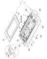
- FIG. 1 is a perspective view of a case 2 according to the present embodiment.
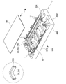
- FIG. 2 is an exploded perspective view of the case 2 according to the present embodiment.
- illustration of a semiconductor element 6 and the like described later is omitted.
- the case 2 includes a first member 3 and a second member 4 that engages with the first member 3 to form a storage space 100 therein.
- the case 2 may be formed in a box shape or a frame shape having the accommodation space 100 inside by the first member 3 and the second member 4, and may be formed in a flat rectangular parallelepiped shape as an example.
- the case 2 may be formed of a resin as a whole.
- the resin for example, one resin selected from polybutylene terephthalate (PBT), polybutyl acrylate (PBA), polyphenylene sulfide (PPS), polyamide (PA) and acrylonitrile butadiene styrene (ABS) can be used.
- the resin may include a filler (eg, a glass filler) to improve strength and / or functionality.
- the first member 3 may be a case main body having the opening 30 of the accommodation space 100.
- the opening 30 is a portion of the accommodation space 100 formed by the first member 3 that opens on the second member 4 side.
- the first member 3 may be a frame or a box located at the lower part of the case 2.
- the first member 3 may have an annular peripheral wall 302 that forms the opening 30.
- the peripheral wall portion 302 has a first side 321, a second side 322, a third side 323, and a fourth side 324, of which the first side 321 and the second side 322 are mutually different. Opposing, preferably parallel. Further, the third side portion 323 and the fourth side portion 324 face each other, preferably in parallel. In the present embodiment, the first side 321 and the second side 322 are shorter than the third side 323 and the fourth side 324.
- a terminal 11 electrically connected to a semiconductor element 6 or the like described later may be embedded in the first side portion 321 to the fourth side portion 324.
- the first member 3 may have a frame portion 31 provided at the opening 30 of the accommodation space 100 and accommodating the second member 4.
- a frame portion 31 having a shape corresponding to the outer shape of the second member 4 may be formed on the inner peripheral portion of the peripheral wall portion 302 so that the second member 4 is fitted inside.
- the first member 3 described above has the projection 350 extending from the first member 3 side to the second member 4 side.
- extending from the first member 3 side to the second member 4 side may mean extending in parallel or substantially parallel to the depth direction of the accommodation space 100 or the height direction of the peripheral wall portion 302.
- the protrusion 350 may extend along the inner surface of the frame 31. More specifically, the protrusion 350 may extend in a state of being separated from the inner surface of the frame portion 31 or may extend in a state in contact with the inner surface of the frame portion 31 or in an integrated state.
- One or more of the protrusions 350 may be provided corresponding to at least a part of the outer edge of the second member 4, for example, two of the positions in the frame 31 facing each other are provided. It may be done.
- one protrusion 350 is provided on each of the first side 321 and the second side 322. More specifically, in the middle part of the first side 321 and the second side 322, a counterbore 310 for mounting the second member 4 is provided at the lower part of the inner periphery of the frame 31 respectively.
- a protrusion 350 may be provided on the upper surface of the counterbore 310.
- the protrusion 350 may be provided on the upper surface of the peripheral wall 302, may be provided on the bottom of the housing space 100 (for example, the upper surface of the heat sink 10 described later), or the inner peripheral surface of the peripheral wall 302 (For example, it may protrude inward from the inner peripheral surface of the frame part 31).
- the projection 350 as described above is connected to the first member 3 via the later-described notch 40 or the through hole 400 in the second member 4.
- the end 351 is exposed on the opposite side (the upper side in the figure, also referred to as the upper side as an example).
- the end 350 is crushed from the upper surface side of the protrusion 350, thereby fixing the second member 4 to the first member 3. The fixing of the first member 3 and the second member 4 will be described in detail later with reference to FIG.
- Such a projection 350 is, for example, one thermoplastic resin selected from polybutylene terephthalate (PBT), polybutyl acrylate (PBA), polyphenylene sulfide (PPS), polyamide (PA), acrylonitrile butadiene styrene (ABS) and the like. And may be formed of The resin may include a filler (eg, a glass filler) to improve strength and / or functionality.
- the protrusion 350 is integrally formed of the same resin material as the first member 3.
- the protrusions 350 may be formed of metal such as solder.
- the second member 4 may be a lid covering the opening 30 of the accommodation space 100, and preferably is fitted into the frame 31 of the first member 3 to cover the accommodation space 100.
- the second member 4 is formed in a rectangular plate shape.
- the second member 4 may have a notch 40 for passing the protrusion 350 on one side of the outer edge.
- the first member 3 and the second member 4 may be fitted, for example, by causing the first member 3 and the second member 4 to face each other so as to allow the protrusion 350 to pass through the notch 40.
- the notch 40 may have a polygonal shape when viewed from the upper surface side, that is, an upper surface view, and has a rectangular shape as an example.
- the notch 40 is engaged with the projection 350 in order to fix the first member 3 and the second member 4.
- the fixing of the first member 3 and the second member 4 will be described later in detail with reference to FIG.
- the housing space 100 of the case 2 may house one or more substrates 5 and one or more semiconductor elements 6 mounted on the one or more substrates 5. Thereby, the semiconductor device 1 including the case 2, the substrate 5 and the semiconductor element 6 is formed.
- the semiconductor device 1 may be, for example, an IGBT module or a power module incorporating a transistor such as an IGBT or a vertical MOSFET or a semiconductor element 6 of a diode such as FWD.
- an IGBT module etc. the inverter apparatus which drives a motor is mentioned.
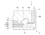
- FIG. 3 is a cross-sectional view showing a state in which the substrate 5 and the semiconductor element 6 are accommodated in the case 2 in the semiconductor device 1 according to the present embodiment.
- the semiconductor device 1 may have a heat sink 10, a terminal 11, a bonding wire 12 and the like.
- the substrate 5 may have an insulating substrate 520, and conductive layers 521 and heat transfer layers 522 formed on the upper and lower surfaces of the insulating substrate 520, respectively.
- the insulating substrate 520 electrically insulates the conductive layer 521 and the lower heat sink 10.
- the insulating substrate 520 is a ceramic plate.
- the conductive layer 521 has a circuit formed of copper foil or the like, and is electrically connected to the upper semiconductor element 6 by the solder 53.
- the heat transfer layer 522 is formed of a metal such as copper and is joined to the heat sink 10 via the solder 53.
- the semiconductor element 6 may have electrodes on both sides. For example, an electrode formed on the surface on the substrate 5 side is electrically connected to the conductive layer 521, and an electrode formed on the surface opposite to the substrate 5 is described later. It may be connected to the terminal 11 via the bonding wire 12.
- each semiconductor element 6 is an IGBT (Insulated Gate Bipolar Transistor) and FWD (Freewheeling diode) that constitute an arm. It may be a wheeling diode).
- the semiconductor element 6 has the emitter electrode as the main electrode on the side of the substrate 5, the collector electrode as the main electrode, the gate electrode as the control electrode, etc. on the side opposite to the substrate 5.
- the control electrode may be connected to the terminal 11 via a bonding wire 12 described later. The connection of other electrodes and the circuit configuration of the semiconductor device 1 will be described in detail later.
- the heat sink 10 cools the semiconductor element 6 through the substrate 5.
- the heat sink 10 may be a metal plate such as a copper plate, and may be adhered to the lower surface of the peripheral wall portion 302 of the first member 3 in a state of covering the inner bottom surface of the case 2.
- the terminal 11 draws the electrode of the semiconductor element 6 (for example, a control electrode such as a gate electrode of an IGBT) to the outside of the case 2.
- the terminal 11 may have a bent L-shape and the middle portion may be embedded in the peripheral wall portion 302. Then, one end of the terminal 11 may extend upward from the upper end of the peripheral wall portion 302, and the other end may extend from the inner peripheral surface of the peripheral wall portion 302 into the interior of the accommodation space 100.
- copper as a conductive material copper alloy (brass, phosphor bronze, C194 copper alloy, etc.), aluminum, copper-aluminum clad material with conductive plating can be used.
- the bonding wire 12 electrically connects a control electrode (for example, a gate electrode) on the upper surface of the semiconductor element 6 and the terminal 11.
- the bonding wire 12 may electrically connect the control electrode and the terminal 11 via the conductive layer 521.
- a bonding wire 12 for example, a bonding wire made of aluminum can be used.
- a gel material 101 may be filled in the accommodation space 100 in which the substrate 5 and the semiconductor element 6 and the like are accommodated in order to protect the bonding wire 12, the terminal 11 and the conductive layer 521 and the like.
- the gel material 101 silicone gel or the like can be used.
- FIG. 4 is a view for explaining fixation of the first member 3 and the second member 4. More specifically, FIGS. 4 (a) and 4 (b) are diagrams showing a state in which the first member 3 and the second member 4 are not fixed, and FIG. 4 (a) is a top view, FIG. (B) is a cross-sectional view taken along the line AA of FIG. 4 (a). Moreover, FIG.4 (c) and FIG.4 (d) are figures which show the state to which the 1st member 3 and the 2nd member 4 were fixed, FIG.4 (c) is an upper side figure, FIG.4 (d) is. FIG. 5 is a cross-sectional view taken along the line B-B in FIG.
- the first member 3 and the second member 4 are fixed to each other by the engagement of the projection 350 and the notch 40.
- the first member 3 is a second member from the first member 3 side in a state where the first member 3 and the second member 4 are not fixed to each other.
- a protrusion 350 extending to the 4 side may be provided on the upper surface of the counterbore 310.
- the protrusion 350 may be formed in a columnar shape, and the end 351 may be tapered toward the upper surface. As a result, when the first member 3 and the second member 4 are made to face each other and fitted, the operation of passing the protrusion 350 through the notch 40 of the second member 4 is facilitated.
- the cross-sectional shape of the protrusion 350 more specifically, the cross-sectional shape in a plane orthogonal to the extending direction of the protrusion 350 is similar to the shape when viewed from the upper surface side of the notch 40. It may be or may be different.
- the protrusion 350 in the present embodiment is a tapered square prism, and the cross-sectional shape is a square.
- the protrusion 350 described above squeezes the end 351 from the upper surface side It may be spread out and engaged with the notch 40 of the second member 4.
- the end 351 of the projection 350 may be radially spread in a plane intersecting the extension direction of the projection 350, and more preferably, the inner wall of the opening 30 in each direction in the plane. It may be spread evenly in the direction except for.
- the second member 4 may have a rectangular notch 40 in the outer edge portion for passing the protrusion 350 in a state where the first member 3 and the second member 4 are not fixed to each other. . As shown in FIGS. 4 (c) and 4 (d), this notch 40 has the crushed end 351 of the protrusion 350 in a state where the first member 3 and the second member 4 are fixed to each other. May be engaged.
- the second member 4 is a locking surface on at least a portion, preferably a plurality of portions, of the adjacent position of the protrusion 350 on the upper surface side, in other words, the adjacent position of the notch 40 for passing the protrusion 350 There may be 42.
- the locking surface 42 is a surface locked by the crushed end 351 of the projection 350, and is locked from the upper surface side, for example, so that the second member 4 is not separated from the first member 3.
- the locking surface 42 is provided to be inclined such that the second member becomes thinner toward the protrusion 350.
- the locking surface 42 may be provided in a step shape so that the second member 4 becomes thinner toward the protrusion 350.
- the upper surface itself of the second member may function as the locking surface 42 without being partially inclined and formed on stairs.
- the second member 4 may have the clearance portion 41 at least at a part of the position adjacent to the protrusion 350. As shown in FIGS. 4 (c) and 4 (d), the clearance portion 41 has the crushed end portion 351 of the projection 350 in a state where the first member 3 and the second member 4 are fixed to each other.
- the clearance portion 41 may be formed by providing a notch in the upper surface of the second member 4 at a position adjacent to the protrusion 350, and as an example, the second member 4 becomes thinner toward the protrusion 350 It is formed by providing the above-mentioned locking surface 42 as described above.
- the clearance portion 41 may be formed by providing a notch in the side end surface of the second member 4 at a position adjacent to the protrusion 350, and the notch portion 40 described above is provided as an example. It may be formed by
- the volume of the space formed by the clearance portion 41 is the same as that of the first member 3 in the projection 350 in the state where the first member 3 and the second member 4 are not fixed to each other. It may be the same as the volume of the end 351 projecting to the opposite side (upper side in FIG. 4 (b)). Thereby, the crushed end 351 of the protrusion 350 may be formed flush with the portion adjacent to the protrusion 350 in the portion on the upper surface side of the second member 4. However, the volume of the space formed by the clearance portion 41 may be smaller or larger than the volume of the end 351.
- the projection 350 of the first member 3 extends from the first member 3 side to the second member 4 side, and the end 351 is crushed from the upper surface side to make the second member 4 the first Since they are fixed to each other to the member 3, the fixing can be performed only by crushing the end 351 of the protrusion 350. Therefore, the manufacture of the device can be facilitated and the lead time of manufacture can be shortened as compared with the case of fixing by an adhesive or an engagement claw. In addition, it is possible to confirm that the first member 3 and the second member 4 are fixed to each other by visually observing the crushed end 351 of the projection 350, so that it is possible to facilitate the detection of the fixing failure. it can.
- FIG. 5 is a circuit diagram showing the semiconductor device 1 according to the present embodiment.
- the semiconductor device 1 is an inverter device of three-phase output, and has six semiconductor elements 6 as an arm for switching.
- the semiconductor device 6 includes, for example, a temperature sensing diode 60 and an RC-IGBT (Reverse Conducting IGBT) device 61.
- the temperature sensing diode 60 is for sensing the temperature of the substrate of the semiconductor element 6.
- the temperature sensing diode 60 has an anode electrode (A) and a cathode electrode (K) as control electrodes on the side of the substrate 5 so that the temperature of the substrate can be measured by measuring the forward voltage. ing.
- the RC-IGBT element 61 has the emitter electrode (E) as the second electrode, the gate electrode (G) as the control electrode, the sense emitter electrode (S), and the emitter electrode (E) opposite to the substrate 5.
- a collector electrode (C) as a first electrode is provided on the substrate 5 side.
- the emitter electrode (E) is used as a second electrode and a control electrode. Further, between the emitter electrode (E) and the collector electrode (C), there is connected a free wheeling diode 62 which causes a current to flow from the emitter electrode (E) to the collector electrode (C).
- the two semiconductor devices 6 form a pair to form a leg 600.
- the positive electrode (P) of the DC power supply is electrically connected to the collector electrode (C) of one of the semiconductor devices 6 (upper semiconductor device 6 in the figure, also referred to as the upper arm in the figure) in each leg 600 There is.
- the negative electrode (N) of the DC power supply is electrically connected to the emitter electrode (E) of the other semiconductor element (the lower semiconductor element 6 in the figure, also referred to as the lower arm).
- the positive electrode (P) and the negative electrode (N) may be provided through the peripheral wall portion 302 of the case 2.
- the emitter electrode (E) of the upper arm semiconductor element 6 and the collector electrode (C) of the lower arm semiconductor element 6 are electrically connected.
- An external output terminal 601 is electrically connected to this connection portion.
- the external output terminal 601 may be provided to penetrate the peripheral wall portion 302 of the case 2.
- control electrode for example, the gate electrode (G), the sense emitter electrode (S), the emitter electrode (E), the anode electrode (A) and the cathode electrode (K) of each semiconductor element 6 It is pulled out of the case 2 through the terminal 11.
- the semiconductor device 1 having such a circuit configuration, when a control signal is input to the gate terminal (G) of each semiconductor element 6 while applying DC power between the positive electrode and the negative electrode, the RC in the semiconductor element 6 is generated.
- the switching operation of the IGBT element 61 is controlled.
- U-phase, V-phase, and W-phase AC signals are output from the external output terminals 601 of the three legs 600. If the temperature measured by the temperature sensing diode 60 is higher than the reference temperature, control may be performed to reduce heat generation by reducing the emitter current.
- FIG. 6 is a flowchart for explaining the method of manufacturing the case 2 according to the present embodiment.
- the first member 3 and the second member 4 are manufactured (S100).
- the end 351 of the protrusion 350 may have a tapered top.
- the substrate 5 and the semiconductor element 6 may be accommodated inside the manufactured first member 3.
- the heat sink 10 may be bonded to the lower surface of the peripheral wall portion 302 in the first member 3.
- the gel material 101 may be filled.
- the first member 3 and the second member 4 are fitted (S102).
- the second member 4 may be fitted to the frame portion 31 of the first member 3.
- the housing space 100 may be formed by the first member 3 and the second member 4.
- the projection 350 of the first member 3 is passed through the notch 40 of the second member 4, and the end 351 of the projection 350 is opposite to the first member 3 than the locking surface 42 of the second member 4. It may protrude to the side.
- the end 351 of the projection 350 of the first member 3 is crushed to fix the second member 4 to the first member 3 (S104).
- the end 351 may be deformed and crushed by at least one of ultrasonic vibration and heating.
- the end 351 deformed at this time may be integrated with the second member 4 or may not be integrated.
- a heat caulking device when the end 351 is deformed by heating, for example, a heat caulking device can be used.
- an ultrasonic caulking device can be used when the end 351 is deformed by ultrasonic vibration.
- the ultrasonic caulking device melts and deforms the end 351 by applying vibration to the end 351 of the protrusion 350 from a resonator called a horn.
- Case 2 is manufactured by the above-described S100 to S104. Here, after the case 2 is manufactured, it may be determined by visual observation from the outside of the case 2 that the first member 3 and the second member 4 are fixed to each other.
- the protrusions 350 may be colored in a color different from that of the second member 4 in advance, or the protrusions 350 may be discolored due to deformation. You may do so.
- the first member 3 and the second member 4 are fixed to each other under the condition that the discoloring is visually recognized regardless of how the protrusion 350 spreads in top view You may judge that it is done.
- the case 2 may be provided with a member covering the end 351 so that the end 351 of the crushed projection 350 can not be seen from the upper surface side.
- a colored film may be attached to one surface of the upper surface of the second member 4, or the projection 350 may be covered in the vicinity of the projection 350 of the first member 3 and / or the second member 4.
- a cover member may be provided.
- the end 351 of the projection 350 provided on the first member 3 and extending from the first member 3 side to the second member 4 side is crushed to make the second member 4 the first member 3.
- the manufacture of the device can be facilitated and the lead time of the manufacture can be shortened.
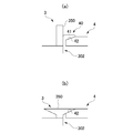
- FIG. 7 is a side view of the protrusion 350 in the modification (1). More specifically, FIG. 7A shows the protrusion 350 in a state in which the first member 3 and the second member 4 are not fixed. Moreover, FIG.7 (b) shows the projection part 350 in the state to which the 1st member 3 and the 2nd member 4 were fixed.
- the projection 350 may be provided on the peripheral wall 302 apart from the inner peripheral edge of the frame 31 (not shown in FIG. 7). Further, as shown in FIG. 7B, in a state in which the first member 3 and the second member 4 are fixed to each other, the end 351 is crushed from the upper surface side, and is directed toward the inside and the outside of the frame 31. Each may be spread out and engaged with the notch 40 of the second member 4.
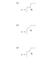
- FIG. 8 is a view showing the notch 40 in the modification (2).
- the notch 40 may be polygonal shape from which the shape when it sees from the upper surface side differs from a square shape.
- the notch 40 may have a trapezoidal shape as shown in FIGS. 8A and 8B, or may have a triangular shape as shown in FIG. 8C.
- the notch 40 may have a shape in which the portion closer to the side of the second member 4 is narrower than the portion farther from the side when viewed from the upper surface, that is, the shape narrows toward the side (See FIG. 8 (a)).
- the portion far from the second member 4 is surrounded by the notch 40, so that the fixation of the first member 3 and the second member 4 becomes strong.
- the portion closer to the side of the second member 4 has a wider shape than the portion farther from the side, that is, a shape that spreads toward the side It is good (refer FIG.8 (b), FIG.8 (c)).
- FIG.8 (b), FIG.8 (c) when fitting the first member 3 and the second member 4 so as to face each other, the operation of passing the projection 350 through the notch 40 of the second member 4 is facilitated.
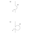
- FIG. 9 is a view showing the notch 40 in the modification (3). As shown in this figure, the notch 40 may have a partially circular shape when viewed from the upper surface side.
- the notch 40 may be semicircular as shown in FIG. 9A, or may be partially circular larger than semicircular as shown in FIG. 9B. Good. Moreover, the notch 40 may be a partial circle smaller than a semicircle. In the case where the notch 40 is a partial circle smaller than a semicircle, the projection 350 can be inserted into the notch 40 of the second member 4 when the first member 3 and the second member 4 are fitted to face each other. Passing work is facilitated. In addition, stress concentration on the engagement portion between the notch 40 and the protrusion 350 is prevented. On the other hand, in the case where the notch 40 is a partial circle larger than a semicircle, the fixation of the first member 3 and the second member 4 becomes strong.
- FIG. 10 is a view showing the notch 40 in the modification (4).
- the notch 40 may be provided at a corner portion of the outer edge of the second member 4.
- the notch 40 may have a polygonal shape when viewed from the upper surface side.
- the notch 40 may have a square shape when viewed from the upper surface side, or may have a triangular shape as shown in FIG. 10 (b). It may be.
- the notch 40 may be partially circular.
- the protrusion 350 may be formed at the corner of the frame 31.
- FIG. 11 is a view showing the notch 40 and the protrusion 350 in the modification (5).
- the notch 40 may be formed uniformly over the entire circumference of the second member 4.
- the second member 4 may be formed smaller by an amount corresponding to the size of the notch 40.
- the projection 350 may surround the entire outer periphery of the second member 4 in a state in which the first member 3 and the second member 4 are fitted facing each other.
- the protrusion 350 may be formed over the entire circumference of the frame 31.
- the protrusion 350 may be formed as the frame 31 and may have an end 351 on the upper surface side.
- the end 351 may be formed to be thinner toward the side opposite to the first member 3, and when the second member 4 is fitted into the frame 31, the end 351 may be thinner than the upper surface of the second member 4. It may project on the opposite side to the one member 3.
- the end 351 is engaged with the second member 4 over the entire outer periphery of the second member 4 by crushing the end 351 from the side opposite to the first member 3, and the second member 4 is a first member. It may be fixed to 3.
- FIG. 12 is a view showing the second member 4 in the modification (6).
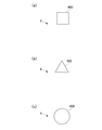
- the second member 4 may have a through hole 400 through which the protrusion 350 passes, in addition to / in place of the notch 40 of the outer edge.
- the through hole 400 may have a polygonal shape when viewed from the upper surface side.
- the through hole 400 may have a square shape when viewed from the upper surface side, or may have a triangular shape as shown in FIG. 12 (b). May be
- the through holes 400 may be circular as shown in FIG. 12 (c).
- the through hole 400 may be provided in the outer peripheral portion of the second member 4 or in the central portion.
- the protrusion 350 is provided at a position opposite to the through hole 400 in the first member 3.
- the protrusion 350 may be provided on the upper surface of the counterbore 310, or may be provided on the bottom surface of the housing space 100 (for example, the upper surface of the heat sink 10).
- the protrusion 350 may be provided so as to protrude inward from the inner peripheral surface of the frame portion 31.
- the protrusion 350 may be provided on the upper surface of a beam member (not shown) provided in the case 2 across the accommodation space 100.
- FIG. 13 is a cross-sectional view showing a state in which the substrate 5 and the semiconductor element 6 are accommodated in the case 2 in the semiconductor device 1 according to the modification (7).
- the semiconductor device 1 may not have the heat sink 10.
- the heat transfer layer 522 of the substrate 5 may be exposed to the inner side of the peripheral wall portion 302 of the case 2 on the side (lower side) opposite to the second member 4.
- the insulating substrate 520 and the peripheral wall portion 302 may be fixed by an adhesive.
- the second member 4 and the first member 3 are fixed in a state in which the second member 4 is fitted in the frame portion 31 of the first member 3. You may fix in the state mounted in the upper surface side.
- the projection 350 may be formed on the upper surface of the peripheral wall 302.
- first member 3 has been described as the case body and the second member 4 as the lid, other members may be used as long as the first member 3 and the second member 4 engage with each other to form the housing space 100 therein. It is good also as a member of shape.
- the first member 3 may be a flat base member
- the second member 4 may be a concave (eg, an ⁇ -shaped) member having an opening on the side of the first member 3.
- the second member 4 has the notch 40 and / or the through hole 400 in the outer peripheral portion
- the first member 3 has the protrusion 350 at the corresponding position of the notch 40 and the through hole 400.
- SYMBOLS 1 semiconductor device 2 case, 3 1st member, 4 2nd member, 5 board
Landscapes
- Engineering & Computer Science (AREA)
- Microelectronics & Electronic Packaging (AREA)
- Cooling Or The Like Of Semiconductors Or Solid State Devices (AREA)
- Structures Or Materials For Encapsulating Or Coating Semiconductor Devices Or Solid State Devices (AREA)
- Casings For Electric Apparatus (AREA)
- Chemical & Material Sciences (AREA)
- Ceramic Engineering (AREA)
Abstract
接着剤によってケース本体と蓋体とを固定する場合には、接着剤を塗布してケース本体および蓋体を貼り合わせ、接着剤を加熱等により硬化させるといった工程が必要となり、装置の製造に手間が掛かってしまう。また、係合爪によってケース本体と蓋体とを固定する場合には、係合爪という微細な形状を形成する分、やはり装置の製造に手間が掛かってしまう。第1部材と、第1部材と係合して内部に収容空間を形成する第2部材とを備え、第1部材は、第1部材側から第2部材側へと延伸し、第1部材とは反対側から端部が潰されて第2部材を第1部材に固定する突起部を有するケースと、このケースを備える半導体装置を提供する。
Description
本発明は、ケース、半導体装置、および、ケースの製造方法に関する。
複数のパワー半導体素子が樹脂製のケースに収容された装置が知られている。このケースは開口部を有して半導体素子を収容する箱状のケース本体と、開口部を覆う蓋体とを備えている。これらのケース本体および蓋体は、接着剤、係合爪、またはボルトによって互いに固定されている(例えば、特許文献1、2参照)。
[特許文献1] 特開平4-342158号公報
[特許文献2] 特開2007-36896号公報
[特許文献3] 特開2009-130169号公報
[特許文献1] 特開平4-342158号公報
[特許文献2] 特開2007-36896号公報
[特許文献3] 特開2009-130169号公報
しかしながら、接着剤によってケース本体と蓋体とを固定する場合には、接着剤を塗布してケース本体および蓋体を貼り合わせ、接着剤を加熱等により硬化させるといった工程が必要となり、装置の製造に手間が掛かってしまう。また、係合爪によってケース本体と蓋体とを固定する場合には、係合爪という微細な形状を形成する分、やはり装置の製造に手間が掛かってしまう。
(項目1)
本発明の第1の態様においては、ケースを提供する。ケースは、第1部材を備えてよい。ケースは、第1部材と係合して内部に収容空間を形成する第2部材を備えてよい。第1部材は、第1部材側から第2部材側へと延伸し、第1部材とは反対側から端部が潰されて第2部材を第1部材に固定する突起部を有してよい。
(項目2)
第1部材は収容空間の開口部を有するケース本体であってよい。第2部材は開口部を覆う蓋体であってよい。
(項目3)
突起部は、第2部材の外縁部の少なくとも一部に対応して設けられてよい。
(項目4)
第2部材は、第2部材の外縁部における辺に、突起部を通すための切欠き部を有してよい。
(項目5)
第2部材は、第2部材の外縁部における角部分に、突起部を通すための切欠き部を有してよい。
(項目6)
切欠き部は、第1部材とは反対側から見た場合の形状が、多角形状および部分円状のいずれかであってよい。
(項目7)
突起部は、第2部材の外周全体を囲ってよい。
(項目8)
第2部材は、突起部を通す貫通孔を有してよい。
(項目9)
貫通孔は、第1部材とは反対側から見た場合の形状が、多角形状および円状のいずれかであってよい。
(項目10)
第2部材は、第1部材とは反対側における突起部に隣接する位置の少なくとも一部に、突起部における第1部材とは反対側から潰された端部によって係止される係止面を有してよい。
(項目11)
第2部材は、第1部材とは反対側において、突起部に隣接する位置の複数の部分に係止面を有してよい。
(項目12)
第2部材は、突起部に隣接する位置の少なくとも一部に、突起部における第1部材とは反対側から潰された端部を収容するクリアランス部を有してよい。
(項目13)
突起部における第1部材とは反対側から潰された端部は、第2部材における第1部材とは反対側の部分のうち、突起部に隣接する位置の部分と面一に形成されてよい。
(項目14)
第1部材は、収容空間の開口部に設けられて第2部材を収容する枠部を有するケース本体であってよい。第2部材は、枠部に嵌め込まれて収容空間を覆う蓋体であってよい。突起部は、枠部の内面に沿って延伸してよい。
(項目15)
突起部は、熱可塑性樹脂で形成されてよい。
(項目16)
本発明の第2の態様においては、半導体装置を提供する。半導体装置は、第1の態様のケースを備えてよい。半導体装置は、ケースの収容空間に収容された基板を備えてよい。半導体装置は、基板に搭載された半導体素子を備えてよい。
(項目17)
半導体装置は、容空間内において基板の上側を封止するゲル材をさらに備えてよい。
本発明の第1の態様においては、ケースを提供する。ケースは、第1部材を備えてよい。ケースは、第1部材と係合して内部に収容空間を形成する第2部材を備えてよい。第1部材は、第1部材側から第2部材側へと延伸し、第1部材とは反対側から端部が潰されて第2部材を第1部材に固定する突起部を有してよい。
(項目2)
第1部材は収容空間の開口部を有するケース本体であってよい。第2部材は開口部を覆う蓋体であってよい。
(項目3)
突起部は、第2部材の外縁部の少なくとも一部に対応して設けられてよい。
(項目4)
第2部材は、第2部材の外縁部における辺に、突起部を通すための切欠き部を有してよい。
(項目5)
第2部材は、第2部材の外縁部における角部分に、突起部を通すための切欠き部を有してよい。
(項目6)
切欠き部は、第1部材とは反対側から見た場合の形状が、多角形状および部分円状のいずれかであってよい。
(項目7)
突起部は、第2部材の外周全体を囲ってよい。
(項目8)
第2部材は、突起部を通す貫通孔を有してよい。
(項目9)
貫通孔は、第1部材とは反対側から見た場合の形状が、多角形状および円状のいずれかであってよい。
(項目10)
第2部材は、第1部材とは反対側における突起部に隣接する位置の少なくとも一部に、突起部における第1部材とは反対側から潰された端部によって係止される係止面を有してよい。
(項目11)
第2部材は、第1部材とは反対側において、突起部に隣接する位置の複数の部分に係止面を有してよい。
(項目12)
第2部材は、突起部に隣接する位置の少なくとも一部に、突起部における第1部材とは反対側から潰された端部を収容するクリアランス部を有してよい。
(項目13)
突起部における第1部材とは反対側から潰された端部は、第2部材における第1部材とは反対側の部分のうち、突起部に隣接する位置の部分と面一に形成されてよい。
(項目14)
第1部材は、収容空間の開口部に設けられて第2部材を収容する枠部を有するケース本体であってよい。第2部材は、枠部に嵌め込まれて収容空間を覆う蓋体であってよい。突起部は、枠部の内面に沿って延伸してよい。
(項目15)
突起部は、熱可塑性樹脂で形成されてよい。
(項目16)
本発明の第2の態様においては、半導体装置を提供する。半導体装置は、第1の態様のケースを備えてよい。半導体装置は、ケースの収容空間に収容された基板を備えてよい。半導体装置は、基板に搭載された半導体素子を備えてよい。
(項目17)
半導体装置は、容空間内において基板の上側を封止するゲル材をさらに備えてよい。
(項目18)
本発明の第2の態様においては、ケースの製造方法を提供する。ケースの製造方法は、第1部材、および第1部材と係合して内部に収容空間を形成する第2部材を製造する段階を備えてよい。ケースの製造方法は、第1部材および第2部材を嵌め合わせる段階を備えてよい。ケースの製造方法は、第1部材に設けられて第1部材側から第2部材側へと延伸する突起部の、第2部材における第1部材とは反対側の面に突出する端部を潰して、第2部材を第1部材に固定する段階を備えてよい。
(項目19)
第2部材を第1部材に固定する段階は、端部を超音波加振および加熱の少なくとも一方により潰してよい。
(項目20)
第1部材および第2部材を製造する段階は、潰す前における端部に先細りの頂部を形成してよい。
本発明の第2の態様においては、ケースの製造方法を提供する。ケースの製造方法は、第1部材、および第1部材と係合して内部に収容空間を形成する第2部材を製造する段階を備えてよい。ケースの製造方法は、第1部材および第2部材を嵌め合わせる段階を備えてよい。ケースの製造方法は、第1部材に設けられて第1部材側から第2部材側へと延伸する突起部の、第2部材における第1部材とは反対側の面に突出する端部を潰して、第2部材を第1部材に固定する段階を備えてよい。
(項目19)
第2部材を第1部材に固定する段階は、端部を超音波加振および加熱の少なくとも一方により潰してよい。
(項目20)
第1部材および第2部材を製造する段階は、潰す前における端部に先細りの頂部を形成してよい。
なお、上記の概要は、本発明の特徴の全てを列挙したものではない。また、これらの特徴群のサブコンビネーションもまた、発明となりうる。
以下、発明の実施の形態を通じて本発明を説明するが、以下の実施形態は請求の範囲にかかる発明を限定するものではない。また、実施形態の中で説明されている特徴の組み合わせの全てが発明の解決手段に必須であるとは限らない。
本実施形態に係るケースは、互いに係合して内部に収容空間を形成する第1部材および第2部材を備える。第1部材は第2部材側へと延伸する突起部を有し、この突起部は、第1部材とは反対側から端部が潰されて第2部材を第1部材に固定する。これにより、突起部の端部を潰すだけで第1部材および第2部材の固定が可能となっている。
[1.ケース]
図1は、本実施形態に係るケース2の斜視図である。また、図2は、本実施形態に係るケース2の分解斜視図である。なお、図2では、後述の半導体素子6等の図示を省略している。
図1は、本実施形態に係るケース2の斜視図である。また、図2は、本実施形態に係るケース2の分解斜視図である。なお、図2では、後述の半導体素子6等の図示を省略している。
ケース2は、第1部材3と、第1部材3と係合して内部に収容空間100を形成する第2部材4とを備える。例えば、ケース2は、これらの第1部材3および第2部材4によって、内部に収容空間100を有する箱状または枠状に形成されてよく、一例として扁平な直方体状に形成されてよい。また、ケース2は、全体として樹脂により形成されてよい。樹脂としては、例えばポリブチレンテレフタラート(PBT)、ポリブチルアクリレート(PBA)、ポリフェニレンサルファイド(PPS)、ポリアミド(PA)およびアクリロニトリルブタジエンスチレン(ABS)等から選ばれる一の樹脂を用いることができる。この樹脂には、強度および/または機能性を向上させるためのフィラー(例えばガラスフィラー)が含まれてもよい。
[1-1.第1部材]
第1部材3は、収容空間100の開口部30を有するケース本体であってよい。開口部30は、第1部材3によって形成される収容空間100のうち、第2部材4側で開口する部分である。一例として、第1部材3は、ケース2の下部に位置する枠または箱であってよい。
第1部材3は、収容空間100の開口部30を有するケース本体であってよい。開口部30は、第1部材3によって形成される収容空間100のうち、第2部材4側で開口する部分である。一例として、第1部材3は、ケース2の下部に位置する枠または箱であってよい。
例えば、第1部材3は、開口部30を形成する環状の周壁部302を有してよい。周壁部302は、第1側部321、第2側部322、第3側部323および第4側部324を有しており、このうち第1側部321と第2側部322とが互いに対向し、好ましくは平行となっている。また、第3側部323と第4側部324とが互いに対向し、好ましくは平行となっている。本実施の形態においては、第1側部321および第2側部322は、第3側部323および第4側部324よりも短くなっている。これらの第1側部321~第4側部324には、後述の半導体素子6等に電気的に接続される端子11が埋め込まれてよい。
また、好ましくは、第1部材3は、収容空間100の開口部30に設けられて第2部材4を収容する枠部31を有してよい。例えば、周壁部302の内周部には、内側に第2部材4が嵌め込まれるよう、第2部材4の外形と対応する形状の枠部31が形成されてよい。
以上の第1部材3は、第1部材3側から第2部材4側へと延伸する突起部350を有している。ここで、第1部材3側から第2部材4側へと延伸するとは、収容空間100の深さ方向または周壁部302の高さ方向などと平行または略平行に延伸することであってよい。一例として、突起部350は、枠部31の内面に沿って延伸してよい。より具体的には、突起部350は、枠部31の内面から離間した状態で延伸してもよいし、枠部31の内面に接した状態または一体化した状態で延伸してもよい。
この突起部350は、第2部材4の外縁部の少なくとも一部に対応して1または複数設けられてよく、例えば、枠部31内の各位置のうち、互いに対向する対向位置に2つが設けられてよい。一例として、突起部350は、第1側部321および第2側部322のそれぞれに1つずつ設けられている。より具体的には、第1側部321および第2側部322の中途部には、第2部材4を載置するための座ぐり部310がそれぞれ枠部31の内周部の下部分に形成され、この座ぐり部310の上面に突起部350が設けられてよい。但し、突起部350は、周壁部302の上面に設けられてもよいし、収容空間100の底面(例えば後述の放熱板10の上面)に設けられてもよいし、周壁部302の内周面(例えば枠部31の内周面)から内側に突出して設けられてもよい。
このような突起部350は、第1部材3および第2部材4が収容空間100を形成した状態において、第2部材4における後述の切欠き部40または貫通孔400を介し、第1部材3とは反対側(図中の上側。一例として上面側とも称する)に端部351が露出している。また、突起部350は、上面側から端部351が潰されており、これにより第2部材4を第1部材3に固定している。なお、第1部材3および第2部材4の固定については、図4を用いて詳細を後述する。
このような突起部350は、例えばポリブチレンテレフタラート(PBT)、ポリブチルアクリレート(PBA)、ポリフェニレンサルファイド(PPS)、ポリアミド(PA)およびアクリロニトリルブタジエンスチレン(ABS)等から選ばれる一の熱可塑性樹脂で形成されてよい。この樹脂には、強度および/または機能性を向上させるためのフィラー(例えばガラスフィラー)が含まれてもよい。好ましくは、突起部350は、第1部材3と同一の樹脂材料によって一体的に形成される。但し、突起部350は半田などの金属で形成されてもよい。
[1-2.第2部材]
第2部材4は、収容空間100の開口部30を覆う蓋体であってよく、好ましくは、第1部材3の枠部31に嵌め込まれて収容空間100を覆う。例えば、第2部材4は、矩形板状に形成される。
第2部材4は、収容空間100の開口部30を覆う蓋体であってよく、好ましくは、第1部材3の枠部31に嵌め込まれて収容空間100を覆う。例えば、第2部材4は、矩形板状に形成される。
この第2部材4は、外縁部における辺(へん)に、突起部350を通すための切欠き部40を有してよい。これにより、例えば切欠き部40に突起部350を通すよう第1部材3および第2部材4を対向させることで、第1部材3および第2部材4が嵌め合わされてよい。切欠き部40は、上面側から見た場合の形状、つまり上面視が多角形状であってよく、一例として方形状となっている。
以上の切欠き部40は、第1部材3と第2部材4とを固定すべく、突起部350と係合するようになっている。第1部材3および第2部材4の固定については、図4を用いて詳細を後述する。
[2.半導体装置]
以上のケース2の収容空間100には、1または複数の基板5と、1または複数の基板5に搭載された1または複数の半導体素子6とが収容されてよい。これにより、ケース2、基板5および半導体素子6を備える半導体装置1が形成される。半導体装置1は、一例として、IGBTまたは縦型MOSFET等のトランジスタやFWD等のダイオードの半導体素子6を内蔵したIGBTモジュールまたはパワーモジュール等であってよい。このようなIGBTモジュール等の一例として、モータを駆動するインバータ装置が挙げられる。
以上のケース2の収容空間100には、1または複数の基板5と、1または複数の基板5に搭載された1または複数の半導体素子6とが収容されてよい。これにより、ケース2、基板5および半導体素子6を備える半導体装置1が形成される。半導体装置1は、一例として、IGBTまたは縦型MOSFET等のトランジスタやFWD等のダイオードの半導体素子6を内蔵したIGBTモジュールまたはパワーモジュール等であってよい。このようなIGBTモジュール等の一例として、モータを駆動するインバータ装置が挙げられる。
図3は、本実施形態に係る半導体装置1においてケース2内に基板5および半導体素子6が収容された状態を示す断面図である。この図に示すように、半導体装置1は、基板5および半導体素子6に加えて、放熱板10と、端子11と、ボンディングワイヤ12等とを有してよい。
基板5は、絶縁基板520と、絶縁基板520の上面及び下面にそれぞれ形成された導電層521および伝熱層522とを有してよい。絶縁基板520は、導電層521と、下部の放熱板10とを電気的に絶縁する。例えば、絶縁基板520は、セラミック板である。導電層521は、銅箔などにより形成された回路を有しており、半田53により上部の半導体素子6に電気的に接続されている。伝熱層522は、銅などの金属で形成されており、半田53を介して放熱板10に接合されている。
半導体素子6は、両面に電極を有してよく、例えば基板5側の面に形成された電極が導電層521に電気的に接続され、基板5とは反対面に形成された電極が後述のボンディングワイヤ12を介して端子11に接続されてよい。一例として、半導体装置1が3相出力のインバータ装置である場合には、各半導体素子6は、アームを構成するIGBT(絶縁ゲートバイポーラトランジスタ;Insulated Gate Bipolar Transistor)およびFWD(フリーホイーリングダイオード;Free Wheeling Diode)であってよい。この場合には、半導体素子6は、主電極としてのエミッタ電極を基板5の側に、主電極としてのコレクタ電極と、制御電極としてのゲート電極などを基板5とは反対側の面に有してよく、このうち制御電極が後述のボンディングワイヤ12を介して端子11に接続されてよい。なお、他の電極についての接続、および、半導体装置1の回路構成については、詳細を後述する。
放熱板10は、基板5を介して半導体素子6を冷却する。例えば、放熱板10は、銅板等の金属板であってよく、ケース2の内部底面を覆った状態で第1部材3における周壁部302の下面に接着されてよい。
端子11は、半導体素子6の電極(例えばIGBTのゲート電極などの制御電極)をケース2の外部へ引き出す。例えば、端子11は、屈曲されたL字状を有して中途部が周壁部302に埋め込まれてよい。そして、端子11の一端が周壁部302の上端から上方に延伸し、他端が周壁部302の内周面から収容空間100の内部に延伸してよい。このような端子11としては、例えば導電材としての銅、銅合金(真鍮、リン青銅、C194銅合金等)、アルミニウム、銅-アルミニウムクラッド材に導電めっきをしたものを用いることができる。
ボンディングワイヤ12は、半導体素子6の上面の制御電極(例えばゲート電極)と、端子11とを電気的に接続する。なお、ボンディングワイヤ12は、導電層521を介して制御電極と、端子11とを電気的に接続してもよい。このようなボンディングワイヤ12としては、例えばアルミニウム製のボンディングワイヤを用いることができる。
なお、基板5および半導体素子6などが収容された収容空間100には、ボンディングワイヤ12、端子11および導電層521等を保護すべく、ゲル材101が充填されてよい。ゲル材101としてはシリコーンゲル等を用いることができる。
[3.第1部材および第2部材の固定]
図4は、第1部材3および第2部材4の固定を説明するための図である。より詳細には、図4(a)、図4(b)は、第1部材3および第2部材4が固定されていない状態を示す図であり、図4(a)が上面図、図4(b)が図4(a)のA-A線断面図である。また、図4(c)、図4(d)は、第1部材3および第2部材4が固定された状態を示す図であり、図4(c)が上面図、図4(d)が図4(c)のB-B線断面図である。
図4は、第1部材3および第2部材4の固定を説明するための図である。より詳細には、図4(a)、図4(b)は、第1部材3および第2部材4が固定されていない状態を示す図であり、図4(a)が上面図、図4(b)が図4(a)のA-A線断面図である。また、図4(c)、図4(d)は、第1部材3および第2部材4が固定された状態を示す図であり、図4(c)が上面図、図4(d)が図4(c)のB-B線断面図である。
これらの図4(a)~図4(d)に示すように、第1部材3および第2部材4は、突起部350と切欠き部40とが係合することで、互いに固定されている。例えば、図4(a)、図4(b)に示すように、第1部材3は、第1部材3および第2部材4が互いに固定されていない状態において第1部材3側から第2部材4側へと延伸する突起部350を、座ぐり部310の上面に有してよい。
この突起部350は、柱状に形成されると共に、上面側に向かって端部351が先細りに形成されてよい。これにより、第1部材3および第2部材4を対向させて嵌め合わせるときに、突起部350を第2部材4の切欠き部40に通す作業が容易化される。なお、突起部350の断面形状、より具体的には、突起部350の延伸方向と直交する面内での断面形状は、切欠き部40の上面側から視た場合の形状に対して相似形であってもよいし、異なっていてもよい。一例として、本実施形態における突起部350は先細りの4角柱状となっており、断面形状が方形状となっている。
以上の突起部350は、図4(c)、図4(d)に示すように、第1部材3および第2部材4が互いに固定された状態では、上面側から端部351が潰されて押し広げられて、第2部材4の切欠き部40と係合してよい。好ましくは、突起部350の端部351は、突起部350の延伸方向と交差する面内で放射状に押し広げられてよく、より好ましくは、当該面内の各方向のうち、開口部30の内壁を除く方向に均等に押し広げられてよい。
一方、第2部材4は、第1部材3および第2部材4が互いに固定されていない状態において突起部350を通すための方形状の切欠き部40を、外縁部における辺に有してよい。この切欠き部40は、図4(c)、図4(d)に示すように、第1部材3および第2部材4が互いに固定された状態では、突起部350の潰された端部351と係合してよい。
また、第2部材4は、上面側における突起部350の隣接位置、別言すれば突起部350を通すための切欠き部40の隣接位置の少なくとも一部、好ましくは複数の部分に係止面42を有してよい。この係止面42は、突起部350における潰された端部351によって係止される面であり、例えば、第2部材4が第1部材3から離れないように上面側から係止される。一例として、係止面42は、第2部材が突起部350の側に向かって薄くなるように、傾斜して設けられている。但し、係止面42は、第2部材4が突起部350の側に向かって薄くなるように、階段状に設けられてもよい。また、第2部材の上面そのものが、部分的に傾斜して形成されたり階段上に形成されたりすることなく、係止面42として機能してもよい。
また、第2部材4は、突起部350の隣接位置の少なくとも一部にクリアランス部41を有してよい。このクリアランス部41は、図4(c)、図4(d)に示すように、第1部材3および第2部材4が互いに固定された状態において、突起部350の潰された端部351を収容する。例えば、クリアランス部41は、突起部350の隣接位置における第2部材4の上面に切欠きを設けることで形成されてよく、一例として、第2部材4が突起部350の側に向かって薄くなるように上述の係止面42を設けることにより形成される。これに加えて/代えて、クリアランス部41は、突起部350の隣接位置における第2部材4の側端面に切欠きを設けることで形成されてよく、一例として、上述の切欠き部40を設けることにより形成されてよい。
なお、クリアランス部41により形成される空間の体積は、第1部材3および第2部材4が互いに固定されていない状態での突起部350において第2部材4の上面よりも第1部材3とは反対側(図4(b)の上側)に突出した端部351の体積と同じであってよい。これにより、突起部350の潰された端部351は、第2部材4における上面側の部分のうち、突起部350の隣接位置の部分と面一に形成されてよい。但し、クリアランス部41により形成される空間の体積は、端部351の体積よりも小さくてもよいし、大きくてもよい。
以上のケース2によれば、第1部材3の突起部350が第1部材3側から第2部材4側へと延伸し、上面側から端部351が潰されて第2部材4が第1部材3に互いに固定されるので、突起部350の端部351を潰すだけで固定を行うことができる。従って、接着剤または係合爪によって固定を行う場合と比較して、装置の製造を容易化し、製造のリードタイムを短縮することができる。また、突起部350の潰れた端部351を目視することで第1部材3および第2部材4が互いに固定されていることを確認することができるため、固定不良の検出を容易化することができる。
[4.回路構成]
図5は、本実施形態に係る半導体装置1を示す回路図である。この図に示すように、例えば半導体装置1は、3相出力のインバータ装置であり、スイッチングを行うアームとしての6つの半導体素子6を有している。
図5は、本実施形態に係る半導体装置1を示す回路図である。この図に示すように、例えば半導体装置1は、3相出力のインバータ装置であり、スイッチングを行うアームとしての6つの半導体素子6を有している。
半導体素子6は、一例として温度センス用ダイオード60およびRC-IGBT(Reverse Conducting IGBT:逆導通IGBT)素子61を有する。温度センス用ダイオード60は、半導体素子6の基板の温度を検知するものである。この温度センス用ダイオード60は、制御電極としてのアノード電極(A)およびカソード電極(K)を基板5側に有しており、順方向電圧を測定することで基板の温度を測定できるようになっている。
RC-IGBT素子61は、第2電極としてのエミッタ電極(E)と、制御電極としてのゲート電極(G)、センスエミッタ電極(S)、および、エミッタ電極(E)とを基板5とは反対側に、第1電極としてのコレクタ電極(C)を基板5側に有している。なお、エミッタ電極(E)は第2電極かつ制御電極として使用される。また、エミッタ電極(E)と、コレクタ電極(C)との間には、エミッタ電極(E)からコレクタ電極(C)に向かって電流を流すフリーホイールダイオード62が接続されている。
これらの半導体素子6は、2つで対をなしてレグ600を構成している。そして、各レグ600における一方の半導体素子6(図中、上側の半導体素子6。上アームとも称する)のコレクタ電極(C)には、直流電源の正電極(P)が電気的に接続されている。また、他方の半導体素子(図中、下側の半導体素子6。下アームとも称する)のエミッタ電極(E)には、直流電源の負電極(N)が電気的に接続されている。例えば正電極(P)および負電極(N)はケース2の周壁部302を貫通して設けられてよい。
また、上アームの半導体素子6のエミッタ電極(E)と、下アームの半導体素子6のコレクタ電極(C)とが電気的に接続されている。この接続部には、外部出力端子601が電気的に接続されている。例えば、外部出力端子601は、ケース2の周壁部302を貫通して設けられてよい。
また、各半導体素子6の制御電極(例えばゲート電極(G)、センスエミッタ電極(S)、エミッタ電極(E)、アノード電極(A)およびカソード電極(K))は、上述のボンディングワイヤ12および端子11を介してケース2の外部に引き出されている。
このような回路構成の半導体装置1においては、正電極および負電極の間に直流電力を印加しつつ各半導体素子6のゲート端子(G)に対して制御信号を入力すると、半導体素子6におけるRC-IGBT素子61のスイッチング動作が制御される。これにより、3つのレグ600の外部出力端子601からU相、V相、W相の交流信号が出力される。なお、温度センス用ダイオード60によって測定される温度が基準温度よりも高い場合には、エミッタ電流を減少させる等して発熱を減少させるよう制御を行ってもよい。
[5.ケースの製造方法]
続いて、ケース2の製造方法について説明する。図6は、本実施形態に係るケース2の製造方法を説明するフローチャートである。
続いて、ケース2の製造方法について説明する。図6は、本実施形態に係るケース2の製造方法を説明するフローチャートである。
この図に示すように、ケース2を製造するには、まず第1部材3および第2部材4を製造する(S100)。例えば、第1部材3の突起部350を形成する場合には、突起部350の端部351に先細りの頂部を形成してよい。これにより、後述のS102において第1部材3および第2部材4を対向させて嵌め合わせるときに、突起部350を第2部材4の切欠き部40に通す作業が容易化される。
ここで、製造された第1部材3の内部には、基板5および半導体素子6などが収容されてよい。また、第1部材3における周壁部302の下面には、放熱板10が接着されてよい。さらに、第1部材3および放熱板10で形成される凹部には、ゲル材101が充填されてよい。端子11が埋め込まれた状態の第1部材3を製造する場合には、例えば、第1部材3を成型する金型内に端子11を配置した後、樹脂を金型内に注入して固化させる、いわゆるインサート成型法を用いてよい。
次に、第1部材3および第2部材4を嵌め合わせる(S102)。例えば、第2部材4を第1部材3の枠部31に嵌め合わせてよい。
これにより、第1部材3および第2部材4によって収容空間100が形成されてよい。また、第1部材3の突起部350が第2部材4の切欠き部40に通され、突起部350の端部351が第2部材4の係止面42よりも第1部材3とは反対側に突出してよい。
次に、第1部材3の突起部350の端部351を潰して、第2部材4を第1部材3に固定する(S104)。例えば、超音波加振および加熱の少なくとも一方によって端部351を変形させて潰してよい。なお、このとき変形された端部351は第2部材4と一体化してもよいし、一体化しなくてもよい。
ここで、加熱により端部351を変形させる場合には、例えば熱カシメ装置を用いることができる。また、超音波加振により端部351を変形させる場合には、例えば超音波カシメ装置などを用いることができる。超音波カシメ装置は、ホーンと呼ばれる共振体から突起部350の端部351に振動を加えることで、端部351を溶融させて変形する。
端部351の変形に超音波加振を用いる場合には、加熱を用いる場合と比較して変形速度の制御が容易であるため、端部351を容易に所望の形状に変形させることができる。また、変形後の端部351の固化を早めることができるため、固化までの間に第1部材3に対する第2部材4の位置がずれてしまうのを防ぐことができる。また、製品の見栄えをよくすることができる。
以上のS100~S104によってケース2が製造される。ここで、ケース2の製造後には、第1部材3および第2部材4が互いに固定されていることを、ケース2の外側からの目視によって判断してよい。
例えば、上面視において突起部350が広がっていることが目視されることを条件として、第1部材3および第2部材4が互いに固定されていると判断してよい。また、上面視において突起部350が広がって切欠き部40を覆っていることが目視されることを条件として、第1部材3および第2部材4が互いに固定されていると判断してもよい。これらの場合には、突起部350の広がり方の確認を容易化すべく、予め突起部350を第2部材4とは異なる色に着色しておいてもよいし、突起部350が変形により変色するようにしてもよい。
また、突起部350が変形により変色する場合には、上面視における突起部350の広がり方とは無関係に、変色が目視されることを条件として、第1部材3および第2部材4が互いに固定されていると判断してもよい。
但し、潰された突起部350の端部351が上面側から見えないように、当該端部351を覆う部材がケース2に設けられてもよい。例えば、第2部材4の上面の一面に有色のフィルムが貼りつけられてもよいし、第1部材3および/または第2部材4における突起部350の近傍に、当該突起部350を覆うためのカバー部材が設けられてもよい。
以上の製造方法によれば、第1部材3に設けられて第1部材3側から第2部材4側へと延伸する突起部350の端部351を潰して第2部材4を第1部材3に固定するので、接着剤または係合爪によって固定を行う場合と比較して、装置の製造を容易化し、製造のリードタイムを短縮することができる。また、突起部350の潰れた端部351を目視することで第1部材3および第2部材4が互いに固定されていることを確認することができるため、固定不良の検出を容易化することができる。
[6.変形例]
続いて、上記の実施形態の変形例について説明する。
続いて、上記の実施形態の変形例について説明する。
[6-1.変形例(1)]
図7は、変形例(1)における突起部350の側面図である。より詳細には、図7(a)は、第1部材3および第2部材4が固定されていない状態での突起部350を示す。また、図7(b)は、第1部材3および第2部材4が固定された状態での突起部350を示す。
図7は、変形例(1)における突起部350の側面図である。より詳細には、図7(a)は、第1部材3および第2部材4が固定されていない状態での突起部350を示す。また、図7(b)は、第1部材3および第2部材4が固定された状態での突起部350を示す。
これらの図に示すように、突起部350は、枠部31(図7では図示せず)の内周縁部から離れて周壁部302に設けられてよい。また、図7(b)に示すように、第1部材3および第2部材4が互いに固定された状態では、端部351は上面側から潰されて、枠部31の内側および外側に向かってそれぞれ押し広げられて、第2部材4の切欠き部40と係合してよい。
[6-2.変形例(2)]
図8は、変形例(2)における切欠き部40を示す図である。この図に示すように、切欠き部40は、上面側から見た場合の形状が方形状とは異なる多角形状であってもよい。例えば、切欠き部40は、図8(a)、図8(b)に示すように、台形状であってよいし、図8(c)に示すように、三角形状であってもよい。
図8は、変形例(2)における切欠き部40を示す図である。この図に示すように、切欠き部40は、上面側から見た場合の形状が方形状とは異なる多角形状であってもよい。例えば、切欠き部40は、図8(a)、図8(b)に示すように、台形状であってよいし、図8(c)に示すように、三角形状であってもよい。
また、切欠き部40は、上面側から見た場合に第2部材4の辺側により近い部分が当該辺側により遠い部分よりも狭い形状、つまり、辺側に向かって狭まる形状であってよい(図8(a)参照)。この場合には、突起部350の外周の内、第2部材4から遠い側の部分までが切欠き部40によって囲まれるため、第1部材3および第2部材4の固定が強固になる。
また、切欠き部40は、上面側から見た場合に第2部材4の辺側により近い部分が当該辺側により遠い部分よりも広い形状、つまり、辺側に向かって広がる形状であってもよい(図8(b)、図8(c)参照)。この場合には、第1部材3および第2部材4を対向させて嵌め合わせるときに、突起部350を第2部材4の切欠き部40に通す作業が容易化される。
[6-3.変形例(3)]
図9は、変形例(3)における切欠き部40を示す図である。この図に示すように、切欠き部40は、上面側から見た場合の形状が部分円状であってもよい。
図9は、変形例(3)における切欠き部40を示す図である。この図に示すように、切欠き部40は、上面側から見た場合の形状が部分円状であってもよい。
例えば、切欠き部40は、図9(a)に示すように、半円状であってもよいし、図9(b)に示すように、半円よりも大きい部分円状であってもよい。また、切欠き部40は半円よりも小さい部分円状であってもよい。切欠き部40が半円よりも小さい部分円状の場合には、第1部材3および第2部材4を対向させて嵌め合わせるときに、突起部350を第2部材4の切欠き部40に通す作業が容易化される。また、切欠き部40および突起部350の係合部分に対する応力集中が防止される。一方、切欠き部40が半円よりも大きい部分円状の場合には、第1部材3および第2部材4の固定が強固になる。
[6-4.変形例(4)]
図10は、変形例(4)における切欠き部40を示す図である。この図に示すように、切欠き部40は、第2部材4の外縁部における角部分に設けられてもよい。例えば、この切欠き部40は、上面側から見た場合の形状が多角形状であってよい。一例として、切欠き部40は、図10(a)に示すように、上面側から見た場合の形状が方形状であってもよいし、図10(b)に示すように、三角形状であってもよい。また、切欠き部40は、図10(c)に示すように、部分円状であってもよい。なお、切欠き部40が第2部材4の外縁部における角部分に設けられる場合には、突起部350は枠部31の角部分に形成されてよい。
図10は、変形例(4)における切欠き部40を示す図である。この図に示すように、切欠き部40は、第2部材4の外縁部における角部分に設けられてもよい。例えば、この切欠き部40は、上面側から見た場合の形状が多角形状であってよい。一例として、切欠き部40は、図10(a)に示すように、上面側から見た場合の形状が方形状であってもよいし、図10(b)に示すように、三角形状であってもよい。また、切欠き部40は、図10(c)に示すように、部分円状であってもよい。なお、切欠き部40が第2部材4の外縁部における角部分に設けられる場合には、突起部350は枠部31の角部分に形成されてよい。
[6-5.変形例(5)]
図11は、変形例(5)における切欠き部40および突起部350を示す図である。この図に示すように、切欠き部40は第2部材4の全周にわたって一様に形成されてもよい。別言すれば、第2部材4が切欠き部40のサイズに対応する分だけ小さく形成されてよい。
図11は、変形例(5)における切欠き部40および突起部350を示す図である。この図に示すように、切欠き部40は第2部材4の全周にわたって一様に形成されてもよい。別言すれば、第2部材4が切欠き部40のサイズに対応する分だけ小さく形成されてよい。
また、突起部350は、第1部材3および第2部材4が対向して嵌合した状態において第2部材4の外周全体を囲ってもよい。例えば、突起部350は、枠部31の全周にわたって形成されてよい。一例として、突起部350は、枠部31として形成されてよく、上面側に端部351を有してよい。この端部351は、第1部材3とは反対側に向かって薄くなるよう形成されてよく、また、枠部31に第2部材4が嵌め込まれるときに、第2部材4の上面よりも第1部材3とは反対側に突出してよい。また、この端部351は、第1部材3とは反対側から端部351が潰されることで第2部材4の外周全体にわたって第2部材4と係合し、第2部材4を第1部材3に固定してよい。
[6-6.変形例(6)]
図12は、変形例(6)における第2部材4を示す図である。この図に示すように、第2部材4は、外縁部の切欠き部40に加えて/代えて、突起部350を通す貫通孔400を有してもよい。例えば、この貫通孔400は、上面側から見た場合の形状が多角形状であってよい。一例として、貫通孔400は、図12(a)に示すように、上面側から見た場合の形状が方形状であってもよいし、図12(b)に示すように、三角形状であってもよい。また、貫通孔400は、図12(c)に示すように、円状であってもよい。また、貫通孔400は、第2部材4の外周部に設けられてもよいし、中央部に設けられてもよい。
図12は、変形例(6)における第2部材4を示す図である。この図に示すように、第2部材4は、外縁部の切欠き部40に加えて/代えて、突起部350を通す貫通孔400を有してもよい。例えば、この貫通孔400は、上面側から見た場合の形状が多角形状であってよい。一例として、貫通孔400は、図12(a)に示すように、上面側から見た場合の形状が方形状であってもよいし、図12(b)に示すように、三角形状であってもよい。また、貫通孔400は、図12(c)に示すように、円状であってもよい。また、貫通孔400は、第2部材4の外周部に設けられてもよいし、中央部に設けられてもよい。
なお、貫通孔400が第2部材4に設けられる場合には、突起部350は第1部材3における貫通孔400との対向位置に設けられる。例えば、突起部350は、座ぐり部310の上面に設けられてもよいし、収容空間100の底面(例えば放熱板10の上面)に設けられてもよいし、周壁部302の内周面(例えば枠部31の内周面)から内側に突出して設けられてもよい。また、突起部350は、収容空間100を横切ってケース2内に設けられる梁部材(図示せず)の上面に設けられてもよい。
[6-7.変形例(7)]
図13は、変形例(7)に係る半導体装置1においてケース2内に基板5および半導体素子6が収容された状態を示す断面図である。
図13は、変形例(7)に係る半導体装置1においてケース2内に基板5および半導体素子6が収容された状態を示す断面図である。
この図に示すように、半導体装置1は、放熱板10を有しなくてもよい。例えば、基板5の伝熱層522がケース2の周壁部302の内側で第2部材4とは反対の側(下側)に露出してよい。絶縁基板520と周壁部302とは、接着剤により固着されてよい。
[6-8.その他の変形例]
なお、上記の実施形態および変形例では、第1部材3は、収容空間100を形成する周壁部302を有することとして説明したが、さらに底部を有してもよい。また、この底部は周壁部302と同一または同種の樹脂で一体成形されてもよいし、他の材料で形成されて接着されてもよい。
なお、上記の実施形態および変形例では、第1部材3は、収容空間100を形成する周壁部302を有することとして説明したが、さらに底部を有してもよい。また、この底部は周壁部302と同一または同種の樹脂で一体成形されてもよいし、他の材料で形成されて接着されてもよい。
また、第2部材4が第1部材3の枠部31に嵌め込まれた状態で第2部材4および第1部材3が固定されることとして説明したが、第2部材4が第1部材3の上面側に載置された状態で固定されてもよい。この場合には、突起部350が周壁部302の上面に形成されてよい。
また、第1部材3をケース本体、第2部材4を蓋体として説明したが、第1部材3および第2部材4が互いに係合して内部に収容空間100を形成する限りにおいて、他の形状の部材としてもよい。例えば、第1部材3を平板状のベース部材とし、第2部材4を、第1部材3の側に開口を有する凹状(一例としてΩ状)の部材としてもよい。この場合には、第2部材4は外周部に切欠き部40および/または貫通孔400を有し、第1部材3は切欠き部40、貫通孔400の対応位置に突起部350を有してよい。
以上、本発明を実施の形態を用いて説明したが、本発明の技術的範囲は上記実施の形態に記載の範囲には限定されない。上記実施の形態に、多様な変更または改良を加えることが可能であることが当業者に明らかである。その様な変更または改良を加えた形態も本発明の技術的範囲に含まれ得ることが、請求の範囲の記載から明らかである。
請求の範囲、明細書、および図面中において示した装置、システム、プログラム、および方法における動作、手順、ステップ、および段階等の各処理の実行順序は、特段「より前に」、「先立って」等と明示しておらず、また、前の処理の出力を後の処理で用いるのでない限り、任意の順序で実現しうることに留意すべきである。請求の範囲、明細書、および図面中の動作フローに関して、便宜上「まず、」、「次に、」等を用いて説明したとしても、この順で実施することが必須であることを意味するものではない。
1 半導体装置、2 ケース、3 第1部材、4 第2部材、5 基板、6 半導体素子、10 放熱板、11 端子、12 ボンディングワイヤ、30 開口部、31 枠部、40 切欠き部、41 クリアランス部、42 係止面、53 半田、60 温度センス用ダイオード、61 RC-IGBT素子、62 フリーホイールダイオード、100 収容空間、101 ゲル材、302 周壁部、310 座ぐり部、321 第1側部、322 第2側部、323 第3側部、324 第4側部、350 突起部、351 端部、400 貫通孔、520 絶縁基板、521 導電層、522 伝熱層、600 レグ、601 外部出力端子
Claims (20)
- 第1部材と、
前記第1部材と係合して内部に収容空間を形成する第2部材と
を備え、
前記第1部材は、前記第1部材側から前記第2部材側へと延伸し、前記第1部材とは反対側から端部が潰されて前記第2部材を前記第1部材に固定する突起部を有する
ケース。 - 前記第1部材は前記収容空間の開口部を有するケース本体であり、
前記第2部材は前記開口部を覆う蓋体である
請求項1に記載のケース。 - 前記突起部は、前記第2部材の外縁部の少なくとも一部に対応して設けられる請求項1または2に記載のケース。
- 前記第2部材は、前記第2部材の外縁部における辺に、前記突起部を通すための切欠き部を有する請求項3に記載のケース。
- 前記第2部材は、前記第2部材の外縁部における角部分に、前記突起部を通すための切欠き部を有する請求項3に記載のケース。
- 前記切欠き部は、前記第1部材とは反対側から見た場合の形状が、多角形状および部分円状のいずれかである請求項4または5に記載のケース。
- 前記突起部は、前記第2部材の外周全体を囲う請求項1から3のいずれか一項に記載のケース。
- 前記第2部材は、前記突起部を通す貫通孔を有する請求項1または2に記載のケース。
- 前記貫通孔は、前記第1部材とは反対側から見た場合の形状が、多角形状および円状のいずれかである請求項8に記載のケース。
- 前記第2部材は、前記第1部材とは反対側における前記突起部に隣接する位置の少なくとも一部に、前記突起部における前記第1部材とは反対側から潰された端部によって係止される係止面を有する請求項1から9のいずれか一項に記載のケース。
- 前記第2部材は、前記第1部材とは反対側において、前記突起部に隣接する位置の複数の部分に前記係止面を有する請求項10に記載のケース。
- 前記第2部材は、前記突起部に隣接する位置の少なくとも一部に、前記突起部における前記第1部材とは反対側から潰された端部を収容するクリアランス部を有する請求項1から11のいずれか一項に記載のケース。
- 前記突起部における前記第1部材とは反対側から潰された端部は、前記第2部材における前記第1部材とは反対側の部分のうち、前記突起部に隣接する位置の部分と面一に形成される請求項12に記載のケース。
- 前記第1部材は、前記収容空間の開口部に設けられて前記第2部材を収容する枠部を有するケース本体であり、
前記第2部材は、前記枠部に嵌め込まれて前記収容空間を覆う蓋体であり、
前記突起部は、前記枠部の内面に沿って延伸する
請求項1から13のいずれか一項に記載のケース。 - 前記突起部は、熱可塑性樹脂で形成されている
請求項1から14のいずれか一項に記載のケース。 - 請求項1から15のいずれか一項に記載のケースと、
前記ケースの前記収容空間に収容された基板と、
前記基板に搭載された半導体素子と、
を備える半導体装置。 - 前記収容空間内において前記基板の上側を封止するゲル材をさらに備える
請求項16に記載の半導体装置。 - 第1部材、および前記第1部材と係合して内部に収容空間を形成する第2部材を製造する段階と、
前記第1部材および前記第2部材を嵌め合わせる段階と、
前記第1部材に設けられて前記第1部材側から前記第2部材側へと延伸する突起部の、前記第2部材における前記第1部材とは反対側の面に突出する端部を潰して、前記第2部材を前記第1部材に固定する段階と
を備える、ケースの製造方法。 - 前記第2部材を前記第1部材に固定する段階は、前記端部を超音波加振および加熱の少なくとも一方により潰す請求項18に記載の製造方法。
- 前記第1部材および前記第2部材を製造する段階は、潰す前における前記端部に先細りの頂部を形成する請求項18または19に記載の製造方法。
Priority Applications (3)
| Application Number | Priority Date | Filing Date | Title |
|---|---|---|---|
| CN201780002961.8A CN108141976B (zh) | 2016-03-22 | 2017-02-07 | 外壳、半导体装置和外壳的制造方法 |
| JP2018507107A JPWO2017163638A1 (ja) | 2016-03-22 | 2017-02-07 | ケース、半導体装置、および、ケースの製造方法 |
| US15/905,753 US10424522B2 (en) | 2016-03-22 | 2018-02-26 | Case, semiconductor device and manufacturing method of case |
Applications Claiming Priority (2)
| Application Number | Priority Date | Filing Date | Title |
|---|---|---|---|
| JP2016-056505 | 2016-03-22 | ||
| JP2016056505 | 2016-03-22 |
Related Child Applications (1)
| Application Number | Title | Priority Date | Filing Date |
|---|---|---|---|
| US15/905,753 Continuation US10424522B2 (en) | 2016-03-22 | 2018-02-26 | Case, semiconductor device and manufacturing method of case |
Publications (1)
| Publication Number | Publication Date |
|---|---|
| WO2017163638A1 true WO2017163638A1 (ja) | 2017-09-28 |
Family
ID=59901102
Family Applications (1)
| Application Number | Title | Priority Date | Filing Date |
|---|---|---|---|
| PCT/JP2017/004460 Ceased WO2017163638A1 (ja) | 2016-03-22 | 2017-02-07 | ケース、半導体装置、および、ケースの製造方法 |
Country Status (4)
| Country | Link |
|---|---|
| US (1) | US10424522B2 (ja) |
| JP (1) | JPWO2017163638A1 (ja) |
| CN (1) | CN108141976B (ja) |
| WO (1) | WO2017163638A1 (ja) |
Families Citing this family (2)
| Publication number | Priority date | Publication date | Assignee | Title |
|---|---|---|---|---|
| TWD206651S (zh) * | 2020-04-24 | 2020-08-21 | 財團法人工業技術研究院 | 功率模組 |
| EP4597550A1 (en) * | 2024-02-05 | 2025-08-06 | Infineon Technologies AG | Housing for a semiconductor module, semiconductor module comprising a housing, and method for assembling a semiconductor module comprising a housing |
Citations (4)
| Publication number | Priority date | Publication date | Assignee | Title |
|---|---|---|---|---|
| JPH04359547A (ja) * | 1991-06-06 | 1992-12-11 | Mitsubishi Electric Corp | 半導体組立装置 |
| JP2005251320A (ja) * | 2004-03-05 | 2005-09-15 | Matsushita Electric Ind Co Ltd | 光ディスク装置 |
| JP2005340700A (ja) * | 2004-05-31 | 2005-12-08 | Omron Corp | 収納ケース及びその組立方法 |
| JP2010521823A (ja) * | 2007-03-19 | 2010-06-24 | コンティ テミック マイクロエレクトロニック ゲゼルシャフト ミット ベシュレンクテル ハフツング | 電子部品を持つハウジング |
Family Cites Families (19)
| Publication number | Priority date | Publication date | Assignee | Title |
|---|---|---|---|---|
| JPH04342158A (ja) | 1991-05-20 | 1992-11-27 | Fuji Electric Co Ltd | 半導体装置のパッケージ |
| US20020179921A1 (en) * | 2001-06-02 | 2002-12-05 | Cohn Michael B. | Compliant hermetic package |
| US6890834B2 (en) * | 2001-06-11 | 2005-05-10 | Matsushita Electric Industrial Co., Ltd. | Electronic device and method for manufacturing the same |
| DE10232566B4 (de) * | 2001-07-23 | 2015-11-12 | Fuji Electric Co., Ltd. | Halbleiterbauteil |
| WO2005086169A1 (en) | 2004-03-05 | 2005-09-15 | Matsushita Electric Industrial Co., Ltd. | Optical disk apparatus |
| CN104925744A (zh) * | 2004-11-04 | 2015-09-23 | 微芯片生物技术公司 | 压入式冷焊密封方法和装置 |
| JP2007036896A (ja) | 2005-07-28 | 2007-02-08 | Kyocera Kinseki Corp | 圧電部品用容器 |
| JPWO2008059693A1 (ja) * | 2006-11-15 | 2010-02-25 | 株式会社大真空 | 電子部品のパッケージ |
| US8069549B2 (en) * | 2007-03-22 | 2011-12-06 | Seiko Epson Corporation | Method for sealing a quartz crystal device |
| EP2019424B1 (de) * | 2007-07-26 | 2016-11-23 | SEMIKRON Elektronik GmbH & Co. KG | Leistungshalbleitermodul mit Dichteinrichtung zum Substratträger und Herstellungsverfahren hierzu |
| JP4901669B2 (ja) * | 2007-09-26 | 2012-03-21 | 株式会社東芝 | 半導体パッケージ及び半導体パッケージの製造方法 |
| JP5292780B2 (ja) | 2007-11-26 | 2013-09-18 | 日産自動車株式会社 | 半導体装置 |
| WO2011109027A1 (en) | 2010-03-05 | 2011-09-09 | Nokia Corporation | Handover of direct peer to peer communication |
| WO2012088471A1 (en) | 2010-12-22 | 2012-06-28 | Veebot, Llc | Systems and methods for autonomous intravenous needle insertion |
| JP5732286B2 (ja) * | 2011-03-16 | 2015-06-10 | ルネサスエレクトロニクス株式会社 | 半導体装置の製造方法 |
| CN102790993B (zh) | 2011-05-19 | 2015-05-20 | 联芯科技有限公司 | 一种小区搜索阶段进行频点功率测量的方法及装置 |
| US9076891B2 (en) * | 2013-01-30 | 2015-07-07 | Texas Instruments Incorporation | Integrated circuit (“IC”) assembly includes an IC die with a top metallization layer and a conductive epoxy layer applied to the top metallization layer |
| JP5795050B2 (ja) * | 2013-12-27 | 2015-10-14 | 田中貴金属工業株式会社 | 気密封止パッケージ部材及びその製造方法、並びに、該気密封止パッケージ部材を用いた気密封止パッケージの製造方法 |
| JP6132034B2 (ja) * | 2014-01-17 | 2017-05-24 | 富士電機株式会社 | 半導体モジュール |
-
2017
- 2017-02-07 WO PCT/JP2017/004460 patent/WO2017163638A1/ja not_active Ceased
- 2017-02-07 CN CN201780002961.8A patent/CN108141976B/zh not_active Expired - Fee Related
- 2017-02-07 JP JP2018507107A patent/JPWO2017163638A1/ja active Pending
-
2018
- 2018-02-26 US US15/905,753 patent/US10424522B2/en not_active Expired - Fee Related
Patent Citations (4)
| Publication number | Priority date | Publication date | Assignee | Title |
|---|---|---|---|---|
| JPH04359547A (ja) * | 1991-06-06 | 1992-12-11 | Mitsubishi Electric Corp | 半導体組立装置 |
| JP2005251320A (ja) * | 2004-03-05 | 2005-09-15 | Matsushita Electric Ind Co Ltd | 光ディスク装置 |
| JP2005340700A (ja) * | 2004-05-31 | 2005-12-08 | Omron Corp | 収納ケース及びその組立方法 |
| JP2010521823A (ja) * | 2007-03-19 | 2010-06-24 | コンティ テミック マイクロエレクトロニック ゲゼルシャフト ミット ベシュレンクテル ハフツング | 電子部品を持つハウジング |
Also Published As
| Publication number | Publication date |
|---|---|
| JPWO2017163638A1 (ja) | 2018-06-14 |
| US10424522B2 (en) | 2019-09-24 |
| CN108141976B (zh) | 2020-05-05 |
| CN108141976A (zh) | 2018-06-08 |
| US20180182678A1 (en) | 2018-06-28 |
Similar Documents
| Publication | Publication Date | Title |
|---|---|---|
| JP5661183B2 (ja) | 半導体装置およびその製造方法 | |
| JP6288254B2 (ja) | 半導体モジュールおよびその製造方法 | |
| JP6764807B2 (ja) | 半導体モジュール | |
| JP6665926B2 (ja) | 半導体装置および半導体装置の製造方法 | |
| US11232905B2 (en) | Capacitor | |
| US9795053B2 (en) | Electronic device and method for manufacturing the electronic device | |
| US20180076053A1 (en) | Semiconductor module and method of manufacturing semiconductor module | |
| US11742251B2 (en) | Power semiconductor device including press-fit connection terminal | |
| CN108336057B (zh) | 半导体装置及其制造方法 | |
| WO2017163638A1 (ja) | ケース、半導体装置、および、ケースの製造方法 | |
| US8174097B2 (en) | Electric sub-assembly | |
| JP6171631B2 (ja) | 電子装置の製造方法 | |
| JP2011253942A (ja) | 半導体装置及びその製造方法 | |
| JP2020184591A (ja) | 半導体装置の製造方法 | |
| WO2019021507A1 (ja) | 半導体装置及び半導体モジュール | |
| JP2009111319A (ja) | 半導体装置および半導体装置の検査方法 | |
| JP2017212344A (ja) | 半導体装置 | |
| JP2025047360A (ja) | 半導体装置 | |
| CN115241175A (zh) | 半导体装置和半导体装置的制造方法 | |
| JP6809171B2 (ja) | 電子機器、電源装置および電子機器の製造方法 | |
| JP2024126061A (ja) | 半導体モジュールの製造方法及び半導体モジュール | |
| JP2024166626A (ja) | 半導体モジュール、および半導体モジュールの製造方法 | |
| JP2015056521A (ja) | 電子装置 | |
| JP2015008214A (ja) | 電子装置 | |
| KR20180049415A (ko) | 파워 모듈 및 그의 패키징 방법 |
Legal Events
| Date | Code | Title | Description |
|---|---|---|---|
| ENP | Entry into the national phase |
Ref document number: 2018507107 Country of ref document: JP Kind code of ref document: A |
|
| NENP | Non-entry into the national phase |
Ref country code: DE |
|
| 121 | Ep: the epo has been informed by wipo that ep was designated in this application |
Ref document number: 17769685 Country of ref document: EP Kind code of ref document: A1 |
|
| 122 | Ep: pct application non-entry in european phase |
Ref document number: 17769685 Country of ref document: EP Kind code of ref document: A1 |