WO2017138386A1 - 樹脂封止装置及び樹脂封止方法並びに樹脂封止用の成形型 - Google Patents
樹脂封止装置及び樹脂封止方法並びに樹脂封止用の成形型 Download PDFInfo
- Publication number
- WO2017138386A1 WO2017138386A1 PCT/JP2017/003171 JP2017003171W WO2017138386A1 WO 2017138386 A1 WO2017138386 A1 WO 2017138386A1 JP 2017003171 W JP2017003171 W JP 2017003171W WO 2017138386 A1 WO2017138386 A1 WO 2017138386A1
- Authority
- WO
- WIPO (PCT)
- Prior art keywords
- mold
- resin
- resin sealing
- film
- substrate
- Prior art date
- Legal status (The legal status is an assumption and is not a legal conclusion. Google has not performed a legal analysis and makes no representation as to the accuracy of the status listed.)
- Ceased
Links
Images






Classifications
-
- H—ELECTRICITY
- H10—SEMICONDUCTOR DEVICES; ELECTRIC SOLID-STATE DEVICES NOT OTHERWISE PROVIDED FOR
- H10P—GENERIC PROCESSES OR APPARATUS FOR THE MANUFACTURE OR TREATMENT OF DEVICES COVERED BY CLASS H10
- H10P72/00—Handling or holding of wafers, substrates or devices during manufacture or treatment thereof
- H10P72/04—Apparatus for manufacture or treatment
- H10P72/0441—Apparatus for sealing, encapsulating, glassing, decapsulating or the like
-
- B—PERFORMING OPERATIONS; TRANSPORTING
- B29—WORKING OF PLASTICS; WORKING OF SUBSTANCES IN A PLASTIC STATE IN GENERAL
- B29C—SHAPING OR JOINING OF PLASTICS; SHAPING OF MATERIAL IN A PLASTIC STATE, NOT OTHERWISE PROVIDED FOR; AFTER-TREATMENT OF THE SHAPED PRODUCTS, e.g. REPAIRING
- B29C43/00—Compression moulding, i.e. applying external pressure to flow the moulding material; Apparatus therefor
- B29C43/02—Compression moulding, i.e. applying external pressure to flow the moulding material; Apparatus therefor of articles of definite length, i.e. discrete articles
- B29C43/18—Compression moulding, i.e. applying external pressure to flow the moulding material; Apparatus therefor of articles of definite length, i.e. discrete articles incorporating preformed parts or layers, e.g. compression moulding around inserts or for coating articles
-
- B—PERFORMING OPERATIONS; TRANSPORTING
- B29—WORKING OF PLASTICS; WORKING OF SUBSTANCES IN A PLASTIC STATE IN GENERAL
- B29C—SHAPING OR JOINING OF PLASTICS; SHAPING OF MATERIAL IN A PLASTIC STATE, NOT OTHERWISE PROVIDED FOR; AFTER-TREATMENT OF THE SHAPED PRODUCTS, e.g. REPAIRING
- B29C43/00—Compression moulding, i.e. applying external pressure to flow the moulding material; Apparatus therefor
- B29C43/32—Component parts, details or accessories; Auxiliary operations
- B29C43/34—Feeding the material to the mould or the compression means
-
- B—PERFORMING OPERATIONS; TRANSPORTING
- B29—WORKING OF PLASTICS; WORKING OF SUBSTANCES IN A PLASTIC STATE IN GENERAL
- B29C—SHAPING OR JOINING OF PLASTICS; SHAPING OF MATERIAL IN A PLASTIC STATE, NOT OTHERWISE PROVIDED FOR; AFTER-TREATMENT OF THE SHAPED PRODUCTS, e.g. REPAIRING
- B29C43/00—Compression moulding, i.e. applying external pressure to flow the moulding material; Apparatus therefor
- B29C43/32—Component parts, details or accessories; Auxiliary operations
- B29C43/36—Moulds for making articles of definite length, i.e. discrete articles
-
- H—ELECTRICITY
- H10—SEMICONDUCTOR DEVICES; ELECTRIC SOLID-STATE DEVICES NOT OTHERWISE PROVIDED FOR
- H10P—GENERIC PROCESSES OR APPARATUS FOR THE MANUFACTURE OR TREATMENT OF DEVICES COVERED BY CLASS H10
- H10P72/00—Handling or holding of wafers, substrates or devices during manufacture or treatment thereof
- H10P72/04—Apparatus for manufacture or treatment
- H10P72/0442—Apparatus for placing on an insulating substrate, e.g. tape
-
- H—ELECTRICITY
- H10—SEMICONDUCTOR DEVICES; ELECTRIC SOLID-STATE DEVICES NOT OTHERWISE PROVIDED FOR
- H10P—GENERIC PROCESSES OR APPARATUS FOR THE MANUFACTURE OR TREATMENT OF DEVICES COVERED BY CLASS H10
- H10P72/00—Handling or holding of wafers, substrates or devices during manufacture or treatment thereof
- H10P72/70—Handling or holding of wafers, substrates or devices during manufacture or treatment thereof for supporting or gripping
- H10P72/72—Handling or holding of wafers, substrates or devices during manufacture or treatment thereof for supporting or gripping using electrostatic chucks
-
- H—ELECTRICITY
- H10—SEMICONDUCTOR DEVICES; ELECTRIC SOLID-STATE DEVICES NOT OTHERWISE PROVIDED FOR
- H10W—GENERIC PACKAGES, INTERCONNECTIONS, CONNECTORS OR OTHER CONSTRUCTIONAL DETAILS OF DEVICES COVERED BY CLASS H10
- H10W72/00—Interconnections or connectors in packages
- H10W72/01—Manufacture or treatment
- H10W72/0198—Manufacture or treatment batch processes
-
- H—ELECTRICITY
- H10—SEMICONDUCTOR DEVICES; ELECTRIC SOLID-STATE DEVICES NOT OTHERWISE PROVIDED FOR
- H10W—GENERIC PACKAGES, INTERCONNECTIONS, CONNECTORS OR OTHER CONSTRUCTIONAL DETAILS OF DEVICES COVERED BY CLASS H10
- H10W74/00—Encapsulations, e.g. protective coatings
-
- H—ELECTRICITY
- H10—SEMICONDUCTOR DEVICES; ELECTRIC SOLID-STATE DEVICES NOT OTHERWISE PROVIDED FOR
- H10W—GENERIC PACKAGES, INTERCONNECTIONS, CONNECTORS OR OTHER CONSTRUCTIONAL DETAILS OF DEVICES COVERED BY CLASS H10
- H10W74/00—Encapsulations, e.g. protective coatings
- H10W74/01—Manufacture or treatment
-
- H—ELECTRICITY
- H10—SEMICONDUCTOR DEVICES; ELECTRIC SOLID-STATE DEVICES NOT OTHERWISE PROVIDED FOR
- H10W—GENERIC PACKAGES, INTERCONNECTIONS, CONNECTORS OR OTHER CONSTRUCTIONAL DETAILS OF DEVICES COVERED BY CLASS H10
- H10W74/00—Encapsulations, e.g. protective coatings
- H10W74/01—Manufacture or treatment
- H10W74/016—Manufacture or treatment using moulds
Definitions
- the present invention relates to a resin molding apparatus, a resin molding method, and a molding die, and in particular, a resin sealing apparatus, a resin sealing method, and a resin sealing used when a chip-shaped electronic device or the like is resin-sealed.
- the present invention relates to a mold for stopping.
- a chip-like electronic device mounted on a substrate corresponding to a functional member using a resin molding technique is made by a cured resin molded using the resin molding technique. Seal with resin.
- the chips include semiconductor chips such as transistors, integrated circuits (ICs), and light emitting diodes (LEDs).
- Examples of the substrate include a semiconductor substrate such as a silicon substrate (Semiconductor wafer), a printed circuit board (PCB), a lead frame, a ceramic substrate, and the like.
- a release film may be used when resin-sealing a chip mounted on a substrate.
- the release film prevents the cured resin from directly attaching to the mold surface of the mold.
- the release film is a resin adhesion prevention film.
- the release film By using the release film, the substrate on which the chip is sealed with resin (molded product; sealed substrate) is easily released from the mold surface of the mold.
- the release film In order to bring the release film into close contact with the mold surface of the mold, the release film is sucked using a vacuum source provided in the resin sealing device and a vent hole provided in the mold and functioning as a suction hole. To do.
- the sucked release film is brought into close contact with the mold surface of the mold (see Patent Document 1).
- the release film is temporarily adsorbed on the mold surface of the mold.
- the sealing resin may enclose the substrate.
- an adhesive tape is prepared and the substrate is adhered to the adhesive tape.
- the adhesive tape with the substrate and the mold surface of the mold are aligned, and the adhesive tape with the substrate is brought into close contact with the mold surface (see Patent Document 2).
- JP-A-11-040593 (paragraph [0029], FIG. 1) JP 2001-217270 A (paragraph [0021], FIG. 2)
- An object of the present invention is to provide a resin sealing device, a resin sealing method, and a molding die for resin sealing, in which a film and a functional member can be brought into close contact with a mold surface of the molding die.
- the resin sealing device is: A mold that opens and closes a mold having at least a first mold, a second mold provided opposite to the first mold, and the first mold and the second mold.
- a resin sealing device including an opening / closing mechanism and a cavity provided in the mold, and used when manufacturing an electronic component including a functional member,
- An electrostatic chuck provided on the mold surface of the first mold; When the mold is viewed along the mold opening / closing direction, an arrangement region in which the film supplied from the outside of the mold is disposed on the mold surface of the first mold so as to overlap the electrostatic chuck.
- the functional member When the electrostatic chuck is energized, the functional member is temporarily fixed to the mold surface of the first mold in a state of being in close contact with the film, In the state in which the mold is closed, at least a part of the main surface of the functional member is immersed in the fluid resin generated from the resin material supplied to the cavity from the outside of the cavity, in the cavity. At least a part of the main surface of the functional member is covered with a cured resin formed by curing the fluid resin.
- a film supply mechanism for disposing the film in the disposition area A member supply mechanism that arranges the functional member over the arrangement region; A resin supply mechanism for supplying the resin material to the mold; There is a mode.
- the film is temporarily fixed to the mold surface of the first mold by energizing the electrostatic chuck. There is a mode.
- the functional member is a semiconductor substrate or a circuit board having a chip mounted on the main surface
- the film is a resin adhesion prevention film, There is a mode.
- the functional member has at least one of a heat dissipation function or an electrostatic shielding function,
- the film is a resin adhesion prevention film, There is a mode.
- the entire surface and side surfaces of the main surface of the functional member are included in the cavity. There is a mode.
- the resin sealing device Comprising at least one molding module having the molding die and the mold opening and closing mechanism;
- the one molding module and another molding module can be attached and detached. There is a mode.
- the resin sealing method is: A step of preparing a molding die having at least a first die and a second die provided opposite to the first die; and the molding die so as to cover a cavity provided in the molding die A step of disposing a film in the disposition region, a step of disposing a functional member over the film, a step of supplying a resin material to the mold, a step of closing the mold, and the resin material A step of filling the cavity with the fluid resin generated from the step, a step of maintaining the mold closed state, and curing the fluid resin in the cavity to form a cured resin.
- a step of opening the mold, and a resin sealing method used when manufacturing an electronic component including the functional member Temporarily fixing the film to the mold surface of the first mold;
- the functional member and the film are brought into close contact with each other, and the mold surface of the first mold and the functional member
- a step of temporarily fixing the functional member with the film sandwiched therebetween In the step of closing the mold, at least a part of the main surface of the functional member is accommodated in the cavity, In the step of molding the cured resin, at least a part of the main surface of the functional member is covered with the cured resin.
- a film supply mechanism In the step of arranging the film in the arrangement area, a film supply mechanism is used, In the step of arranging the functional member, a member supply mechanism is used, In the step of supplying the resin material, a resin supply mechanism is used. There is a mode.
- the functional member is a semiconductor substrate or a circuit board having a chip mounted on the main surface
- the film is a resin adhesion prevention film, There is a mode.
- the functional member has at least one of a heat dissipation function or an electrostatic shielding function,
- the film is a resin adhesion prevention film, There is a mode.
- the entire surface and side surfaces of the functional member are covered with the cured resin. There is a mode.
- a molding die for resin sealing is: The first mold, the second mold provided opposite to the first mold, the first mold, and the second mold are used when sealing the resin including the functional member.
- a mold for resin sealing used in manufacturing an electronic component having at least a cavity provided in at least one of the molds, An electrostatic chuck provided on the mold surface of the first mold; A film is arranged in an arrangement region in the mold surface of the first mold; The functional member is placed over the film, When the electrostatic chuck is energized, the functional member is temporarily fixed to the mold surface of the first mold in a state of being in close contact with the film, In a state where the mold is closed, at least a part of the main surface of the functional member is covered with the cured resin formed by curing the fluid resin filled in the cavity.
- the film is temporarily fixed to the mold surface of the first mold. There is a mode.
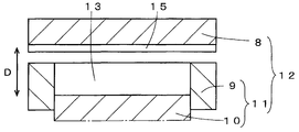
- the resin sealing device according to the present invention it is a schematic cross-sectional view showing a first process in a process of holding a release film and a substrate on which a chip is mounted on an upper mold surface.
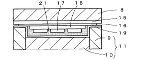
- the resin-sealing device according to the present invention it is a schematic cross-sectional view showing a second process in a process of holding a release film and a substrate on which a chip is mounted on an upper mold surface.
- the resin-sealing device in the resin-sealing device according to the present invention, it is a schematic cross-sectional view showing a third process in a process of holding a release film and a substrate on which a chip is mounted on an upper mold surface. It is a schematic sectional drawing which shows the 1st process in the process of resin-sealing a board
- an electrostatic chuck 15 is provided on the mold surface of the upper mold 8 in the resin sealing apparatus.
- the release film 16 and the substrate 18 on which the chip 17 is mounted are attracted sequentially or simultaneously by an attractive force caused by static electricity.
- the substrate 18 and the release film 16 are held in close contact with the mold surface of the upper mold 8 in a state where the substrate 18 and the release film 16 are in close contact with each other.
- the substrate 18 and the chip 17 mounted on the substrate 18 are immersed in the molten resin 20 filled in the cavity 13.
- the substrate 18 When viewed from above (when viewed along the mold opening / closing direction D), the substrate 18 is included in the cavity 13, so that the substrate 18 and the chip 17 are completely immersed in the molten resin 20. Therefore, the upper surface and side surfaces of the substrate 18 and the chip 17 are covered with the cured resin 21 when the resin sealing is completed.
- Example 1 The configuration of the molding module provided in the resin sealing device according to the present invention will be described with reference to FIGS. 1A to 1B. Any figure in the present application document is schematically omitted or exaggerated as appropriate for easy understanding. About the same component, the same code
- a resin sealing device 1A shown in FIG. 1A is a resin sealing device by a compression molding method.
- the molding module 2 has a lower base 3.
- the four tie bars 4 that are support members are fixed.
- An upper base 5 opposite to the lower base 3 is fixed to the upper part of the four tie bars 4 extending upward.
- an elevator board 6 facing the lower base 3 and the upper base 5 is fitted into the four tie bars 4.
- a mold opening / closing mechanism 7 is fixed on the lower base 3.
- the mold opening / closing mechanism 7 is a drive mechanism that moves the elevator 6 up and down in order to perform mold opening and closing along the mold opening / closing direction D.
- the mold opening / closing mechanism 7 for example, a combination of a servo motor and a ball screw, a combination of a hydraulic cylinder and a link mechanism, or the like is used.
- the elevator 6 is raised or lowered by the mold opening / closing mechanism 7.
- the upper mold 8 is fixed to the lower surface of the upper base 5.
- a frame-shaped peripheral surface member 9 is provided directly below the upper die 8 so as to face the upper die 8.
- the upper surface of the circumferential member 9 faces the lower surface of the upper mold 8.
- a rectangular through hole is provided in the central portion of the circumferential member 9 when viewed in plan.
- a bottom surface member 10 having a rectangular planar shape is provided to be fitted into the through hole of the peripheral surface member 9.
- the bottom member 10 can be moved up and down relative to the circumferential member 9.
- the peripheral surface member 9 and the bottom surface member are collectively driven up and down by the mold opening / closing mechanism 7 and the elevator board 6.
- the peripheral surface member 9 and the bottom surface member 10 are included in the lower mold 11.
- the upper mold 8 and the lower mold 11 are included in one set of molds 12 (hereinafter simply referred to as “molding mold 12”).
- the molding die 12 may include an intermediate die provided between the upper die 8 and the lower die 11.
- the upper mold 8 and the lower mold 11 are appropriately provided with heaters (not shown) as heating means.
- a cavity 13 is formed which is a space in which a cured resin is molded.
- the cavity 13 has a rectangular planar shape.
- a portion surrounding the cavity 13 is referred to as “side surface of the cavity”, and a portion constituting the bottom of the cavity 13 is referred to as “inner bottom surface of the cavity”.
- the side surface of the cavity 13 is constituted by the inner peripheral surface of the peripheral surface member 9.
- the inner bottom surface of the cavity 13 is constituted by the top surface (upper surface in the figure) of the bottom surface member 10.
- the cavity 13 is a space surrounded by the inner peripheral surface of the peripheral surface member 9 and the top surface of the bottom surface member 10.
- a bottom member 10 is fixed to the top surface of the elevator board 6.
- a plurality of elastic bodies (coil springs, disk springs, etc.) 14 are placed around the bottom surface member 10 on the upper surface of the elevator board 6.
- the circumferential member 9 is placed on the plurality of elastic bodies 14.
- the peripheral surface member 9 is elastically supported by the plurality of elastic bodies 14.
- the lower mold 11 (the peripheral surface member 9 and the bottom surface member 10) is moved up and down by the lifting and lowering plate 6 being moved up and down by the mold opening / closing mechanism 7.
- a plurality of elastic bodies may be provided between the bottom member 10 and the elevator board 6.
- An independent drive mechanism different from the mold opening / closing mechanism 7 may be provided on the upper surface of the elevator board 6.
- the following two configurations can be adopted.
- an independent drive mechanism is provided in a space between the upper surface of the elevator board 6 and the lower surface of the bottom member 10.
- An independent drive mechanism raises and lowers the bottom member 10.
- an independent drive mechanism is provided in a space between the upper surface of the elevator board 6 and the lower surface of the circumferential member 9.
- An independent drive mechanism raises and lowers the circumferential member 9.
- an electrostatic chuck (electrostatic chuck: ESC) 15 is provided on a mold surface of the upper mold 8 (the lower surface in FIGS. 1A and 1B).
- the phrase “the electrostatic chuck 15 is provided on the mold surface” includes the following two modes. First, the surface (surface) of the electrostatic chuck 15 constitutes the mold surface of the upper mold 8. Second, the surface of the protective layer covering the surface of the electrostatic chuck 15 constitutes the mold surface of the upper mold 8. This protective layer is composed of a thin metal plate, a resin plate, or the like.
- the electrostatic chuck 15 to which the voltage is applied (energized) uniformly attracts the entire object by an attractive force caused by static electricity.
- the energized electrostatic chuck 15 holds the object in close contact with the surface of the electrostatic chuck 15.
- the electrostatic chuck 15 is different from a mechanical chuck using a vacuum chuck using a suction hole and a rotating claw that holds an object locally and mechanically.
- the electrostatic chuck 15 described in this application document includes all of a Coulomb force electrostatic chuck, a Johnson-Rahbek (JR) force electrostatic chuck, and a gradient force electrostatic chuck.
- the term “an electrostatic chuck that is energized” includes “an electrostatic chuck in which an attractive force due to a charge remaining after voltage application is stopped”.
- a thin, soft and flexible film, a thin and easily damaged member, and the like can be held in close contact with the mold surface of the upper mold 8.
- the entire surface of the large-area object can be held in close contact with the mold surface of the upper mold 8.
- the entire object is attracted by the attractive force caused by static electricity and is brought into close contact with the mold surface of the upper mold 8, so that mechanical adverse effects on the object (for example, scratches, chips, cracks, deformation, etc.) ) Can be reduced.
- the electrostatic chuck 15 By using the electrostatic chuck 15, a wide range of objects such as conductors, semiconductors, and insulators can be held on the mold surface of the upper mold 8. In addition, by using the electrostatic chuck 15, it is possible to hold the laminate on the mold surface of the upper mold 8, which is impossible with the conventional vacuum chuck. For example, a laminate of a release film and a substrate on which a semiconductor chip is mounted, a laminate of a release film and a semiconductor wafer, and the like can be held on the mold surface of the upper mold 8.
- the term “lamination” means that a plurality of members are overlapped with each other and are not fixed to each other.
- a release film 16 is used.
- the release film 16 does not have adhesiveness.
- a resin material having characteristics such as heat resistance, release properties, flexibility, and extensibility is used.
- PTFE, ETFE, PET, FEP, polypropylene, polystyrene, polyvinylidene chloride, or the like is used.
- the release film 16 either a release film cut into a strip shape or a long (roll-shaped) release film continuously supplied from the film supply reel to the film take-up reel is used.
- the mold 12 (the upper mold 8 and the lower mold 11) is opened.
- the release film 16 is transported to a predetermined position below the upper mold 8 using a release film supply mechanism (see FIG. 4).
- the release film supply mechanism uses the release film supply mechanism to raise the release film 16 from a predetermined position.
- the release film 16 is pressed against the placement area AR virtually provided on the mold surface of the upper mold 8. It is preferable to prevent the release film 16 from sagging, wavy, wrinkled or the like by applying tension to the release film 16 at a predetermined position below the upper mold 8.
- the release film is arranged in the arrangement area AR in the mold surface of the upper mold 8.
- the release film 16 and the roll-shaped release film include the cavity 13 in plan view.
- a predetermined voltage is applied to the electrostatic chuck 15.
- This voltage is a voltage (adhesion voltage) for attracting and releasing the release film 16 to the mold surface of the upper mold 8.
- the release film 16 is attracted to the mold surface of the upper mold 8 by using the electrostatic chuck 15 to which the adhesion voltage is applied.
- the release film 16 is held on the mold surface of the upper mold 8 by the electrostatic chuck 15. Since the release film 16 is attracted by the attractive force caused by static electricity using the electrostatic chuck 15, the release film 16 can be held in close contact with the mold surface of the upper mold 8.
- This step corresponds to a step of temporarily fixing the release film 16 to the mold surface of the upper mold 8.
- a substrate (hereinafter referred to as “functional member” as appropriate) 18 is transported to below the upper mold 8 using a substrate transport mechanism (see FIG. 4).
- the substrate 18 is a pre-sealing substrate on which the chip 17 is mounted on the main surface (the lower surface in the figure).
- the substrate transport mechanism aligns the substrate 18 at a predetermined position below the upper mold 8 and stops.
- the electrodes of the chip 17 and the electrodes of the substrate 18 are electrically connected by bonding wires or bumps made of, for example, a gold wire or a copper wire.
- the substrate 18 on which the chip 17 is mounted is a fixed object that is temporarily fixed to the mold surface of the upper mold 8.
- the substrate 18 is raised and the back surface of the substrate 18 is brought into contact with the release film 16. With the back surface of the substrate 18 in contact with the release film 16, the substrate 18 is further raised using the substrate transport mechanism. As a result, the substrate 18 is pressed against the mold surface of the upper mold 8 with the release film 16 interposed therebetween.
- the substrate 18 is attracted by an attractive force caused by static electricity.
- This step corresponds to a step of temporarily fixing the substrate 18 to the mold surface of the upper mold 8.
- the process of temporarily fixing the release film 16 to the mold surface of the upper mold 8 and the process of temporarily fixing the substrate 18 to the mold surface of the upper mold 8 are sequentially performed.
- the substrate 18 and the release film 16 are held in close contact with the mold surface of the upper mold 8 by the electrostatic chuck 15.
- the mold release film 16 and the substrate 18 are held on the mold surface of the upper mold 8 in a state where the mold release film 16 and the substrate 18 are laminated. be able to.
- the size of the functional member is included in the size of the cavity 13 when viewed along the mold opening / closing direction D in order to increase the number of products manufactured from one functional member. Set to In other words, the size is set such that the functional member is accommodated in the cavity 13 in plan view.
- a predetermined amount of resin material is supplied in advance on the upper surface of the release film 19 (see FIG. 3A) outside the mold 12. Thereafter, the release film 19 and the resin material are collectively conveyed to the upper side of the cavity 13 and supplied to the cavity 13.
- a resin such as powder, granule, granule, sheet, paste, jelly, or solid, or a resin that is liquid at room temperature
- the liquid resin is a fluid resin having fluidity at room temperature. It does not matter the degree of fluidity that the liquid resin has at room temperature.
- the present embodiment shows an example in which a molten resin 20 is produced by melting a granular resin (granular resin) supplied as a resin material (see FIG. 3A).
- the resin material supplied to the cavity 13 is heated using a heater (not shown), thereby generating a molten resin 20.
- the molten resin 20 is a fluid resin.
- the cavity 13 is filled with the molten resin 20.
- the elevator 6 is raised using the mold opening / closing mechanism 7 (see FIGS. 1A and 1B).
- the upper surface of the circumferential member 9 is pressed against the electrostatic chuck 15 provided on the upper die 8.
- release films 16 and 19 are interposed between the upper surface of the circumferential member 9 and the electrostatic chuck 15.
- the release films 19 and 16 are sequentially sandwiched between the upper surface of the peripheral surface member 9 and the electrostatic chuck 15, so that the peripheral surface member The upper surface of 9 is pressed against the electrostatic chuck 15.
- the upper mold 8 and the lower mold 11 are closed.
- the substrate 18 and the chip 17 mounted on the substrate 18 are immersed in the molten resin 20 filled in the cavity 13.
- the planar shape of the substrate 18 is included in the planar shape of the cavity 13. Therefore, the chip 17 and the main surface of the substrate 18 (the surface on which the chip 17 is mounted and the lower surface in the drawing) and the side surface can be completely immersed in the molten resin 20.
- the elevator board 6 (see FIGS. 1A and 1B) is further raised.
- the bottom surface member 10 With the upper surface of the peripheral surface member 9 pressing the surface (the lower surface in the figure) of the electrostatic chuck 15 with the release films 19 and 16 in between, the bottom surface member 10 is raised by a predetermined distance.
- pressure is applied to the molten resin 20 in the cavity 13.
- the molten resin 20 is subsequently heated to cure the molten resin 20 and form the cured resin 21.
- the substrate 18 and the chip 17 attached to the substrate 18 are resin-sealed with a cured resin (sealing resin) 21. At this point, the chip 17 and the upper surface and side surfaces of the substrate 18 are covered with the cured resin 21.
- the lower mold 11 is lowered using the mold opening / closing mechanism (see FIGS. 1A and 1B). Thereby, the upper mold 8 and the lower mold 11 are opened. The application of the contact voltage to the electrostatic chuck 15 is stopped. Thereafter, the molded product (sealed substrate) 22 is taken out from the upper mold 8 using a substrate transport mechanism (see FIG. 4).
- the molded product 22 is cut for each region where each chip 17 is mounted.
- a cutting device (not shown)
- the molded product 22 is cut for each region where each chip 17 is mounted.
- a plurality of products 23 corresponding to the plurality of regions are manufactured.
- Each product 23 corresponds to an electronic component.
- the molded product 22 itself may correspond to one electronic component.
- the electrostatic chuck 15 is provided on the mold surface of the upper mold 8.
- the electrostatic chuck 15 attracts the entire object by an attractive force caused by static electricity, and holds it in close contact with the mold surface of the upper mold 8. Therefore, first, a thin, soft and flexible film, a thin and easily damaged member, and the like can be held in close contact with the mold surface of the upper mold 8. Second, the entire surface of the large-area object can be held in close contact with the mold surface of the upper mold 8. Thirdly, since the entire object is attracted by the attractive force caused by static electricity and is uniformly adhered to the mold surface of the upper mold 8, the mechanical force applied to the object is compared with the case where a vacuum chuck and a mechanical clamp are used. Adverse effects can be reduced.
- a laminated body for example, a laminated body of the release film 16 and the substrate 18 or a laminated body of the release film 16 and the semiconductor wafer
- the mold surface of the upper mold 8 Can be held in close contact with each other.
- the structure of the mold can be simplified as compared with the case where a mechanical clamp or a vacuum chuck is used, the manufacturing cost of the resin sealing device can be reduced.
- the release film 16 covers the mold surface of the upper mold 8 so as to include the planar shape of the substrate 18.
- a plate member or lid member made of a metal plate, a fibrous porous metal plate, a conductive resin plate, or the like, and a film are used. You may prepare the laminated body laminated
- the conductive member corresponds to a functional member and has at least one of a heat dissipation function or an electrostatic shielding function.
- the planar shape of the substrate 18 may include the planar shape of the cavity 13.
- the molded product 22 is cut for each region where each chip 17 is mounted. Thereby, a plurality of products 23 are manufactured.
- a second configuration one region corresponding to the product is formed on the substrate 18, and the molded product 22 is cut along the outer periphery of the region. Thereby, one product 23 is manufactured.
- the cured resin 21 is formed on at least a part of the main surface of the substrate 18. “Molding the cured resin 21 on at least a part of the main surface of the substrate 18” includes the following three modes. In the first aspect, a part of the inside of the main surface of the substrate 18 is covered with the cured resin 21 when viewed in plan. In the second aspect, when viewed in a plan view, all portions of the main surface of the substrate 18 are covered with the cured resin 21, and the side surfaces are not covered with the cured resin 21. In the third aspect, when viewed in plan, all portions of the main surface of the substrate 18 are covered with the cured resin 21 and the side surfaces are covered with the cured resin 21. In this embodiment, as shown in FIGS.
- the release film 16 and the substrate 18 are supplied to the upper mold 8 using separate supply mechanisms (release film supply mechanism and substrate transport mechanism). Not limited to this, the same substrate transport mechanism is used, and in the state where the release film 16 is placed on the back surface of the substrate 18 (upper surface in FIG. 2C), the substrate 18 and the release film 16 are collectively placed in the upper mold. 8 can be supplied.
- the release film 19 may be supplied above the cavity 13.
- a suction hole and a suction mechanism both not shown
- the release film 19 is adsorbed and adhered to the mold surface in the cavity 13.
- a resin material is supplied to a space surrounded by the release film 19 in the cavity 13 (this space is referred to as the cavity 13 for convenience).
- the release film 19 may not be used. In this case, the resin material is directly supplied to the cavity 13 surrounded by the exposed mold surface.
- the following method may be adopted. That is, the release film 16 and the substrate 18 are laminated below the upper die 8, and the laminate composed of the release film 16 and the substrate 18 is attracted and held substantially simultaneously on the die surface of the upper die 8. This is the method. In this case, the process of temporarily fixing the release film 16 to the mold surface of the upper mold 8 and the process of temporarily fixing the substrate 18 to the mold surface of the upper mold 8 are performed simultaneously. The When the release film 16 and the substrate 18 are simultaneously attracted to the mold surface of the upper mold 8, the applied voltage can be determined in consideration of the weight and the flat area of the laminate.
- the voltage (applied voltage) applied to the electrostatic chuck 15 may be determined as follows.
- the weight of the substrate 18 is larger than the weight of the release film 16 when compared per unit plane area. From this, when the release film 16 and the substrate 18 are sequentially attracted to the mold surface of the upper mold 8, the substrate 18 is more than the applied voltage when the mold release film 16 is held on the mold surface of the upper mold 8.
- the applied voltage at the time of holding on the mold surface of the upper mold 8 may be increased.
- a voltage that has substantially the same absolute value as that of the contact voltage and has a positive / negative polarity opposite may be applied.
- This applied voltage is a charge removal voltage for removing the charge remaining on the electrostatic chuck 15.
- An appropriate amount of charge may be left by setting the charge removal voltage to an appropriate level.
- a plurality of suction holes are provided in the mold surface in a region outside the electrostatic chuck 15 and outside the functional member in plan view.
- a plurality of electrostatic chucks 15 may be provided in a region inside the functional member in plan view, and a plurality of suction holes may be provided in a mold surface between the electrostatic chucks 15.
- the plurality of suction holes are connected to a decompression source such as a suction pump or a decompression tank via a pipe and an on-off valve, respectively.
- a drive source and a control signal may be supplied to the resin sealing device 1A from the outside of the resin sealing device 1A.
- the driving source include electric power and high-pressure gas (compressed air or the like).
- Predetermined electric power is supplied to at least the mold opening / closing mechanism 7, the electrostatic chuck 15, and a heater (not shown).
- a control signal received from an operation unit (control unit) operated by an operator is supplied to at least the mold opening / closing mechanism 7, the electrostatic chuck 15, and the heater.
- the mold opening / closing mechanism 7, the electrostatic chuck 15, and the heater are controlled by the received control signal.
- an operator, a robot, or the like supplies the release film 16, the substrate 18, and a resin material (not shown) to the resin sealing device 1A.
- the resin sealing device 1A operates according to the received drive source and control signal.
- Resin sealing device 1A can be provided with a power source and a control unit (both not shown). In this case, the resin sealing device 1A itself can operate.
- a resin sealing device 1B according to the present invention will be described with reference to FIG.
- a resin sealing device 1B shown in FIG. 4 is a resin sealing device by a compression molding method.
- the resin sealing device 1B includes a substrate supply / storage module 24, three molding modules 25A, 25B, and 25C, and a material supply module 26 as components.
- the substrate supply / storage module 24, the molding modules 25A, 25B, and 25C, and the material supply module 26, which are constituent elements, can be attached to and detached from each other and exchanged with each other. be able to.
- Each molding module 25A, 25B, 25C may correspond to the resin sealing device 1A shown in FIG. 1A.
- the substrate supply / storage module 24 includes a pre-sealing substrate supply unit 28 for supplying the pre-sealing substrate 27, a sealed substrate storage unit 30 for storing the sealed substrate 29, the pre-sealing substrate 27, and the sealing.
- a substrate platform 31 for delivering the stopped substrate 29 and a substrate transport mechanism 32 for transporting the pre-sealing substrate 27 and the sealed substrate 29 are provided.
- the substrate platform 31 moves in the Y direction within the substrate supply / storage module 24.
- the substrate transport mechanism 32 moves in the X direction, the Y direction, and the Z direction within the substrate supply / storage module 24 and the respective molding modules 25A, 25B, and 25C.
- the predetermined position S1 is a position to stand by when the substrate transport mechanism 32 does not operate.
- Each molding module 25A, 25B, and 25C is provided with a lower mold 11 that can be moved up and down and an upper mold 8 that is disposed opposite to the lower mold 11 (see FIG. 1A).
- the upper die 8 is provided with an electrostatic chuck 15 (see FIGS. 1A and 1B).
- a release film supply mechanism 33 (a rectangular portion indicated by a two-dot chain line in FIG. 4) for supplying the long release film 16 (see FIG. 2B) to the upper mold 8 is provided.
- Each of the molding modules 25A, 25B, and 25C includes a mold opening / closing mechanism 7 (a circular portion indicated by a two-dot chain line in FIG. 4) that opens and closes the upper mold 8 and the lower mold 11.
- a cavity 13 to which the release film 19 and the resin material are supplied is provided in the lower mold 11 (see FIGS. 3A to 3C).
- the material supply module 26 includes an XY table 34, a release film supply mechanism 35 that supplies a release film 19 (see FIGS. 3A to 3C) onto the XY table 34, and a resin storage frame 36.
- a resin material feeding mechanism 37 for feeding the resin material and a resin transport mechanism 38 for transporting the resin housing frame 36 are provided.
- the XY table 34 moves in the X direction and the Y direction in the material supply module 26.
- the resin transport mechanism 38 moves in the X direction, the Y direction, and the Z direction within the material supply module 26 and the respective molding modules 25A, 25B, and 25C.
- the predetermined position M1 is a position to stand by when the resin transport mechanism 38 is not operating.
- the substrate supply / storage module 24 is provided with a control unit CTL.
- the control unit CTL controls the transport of the pre-sealing substrate 27 and the sealed substrate 29, the transport of the resin material, the heating of the mold, the opening and closing of the mold.
- the control unit CTL controls the start and stop of energization of the electrostatic chuck 15 shown in FIGS. 2A to 2C and FIGS. 3A to 3C, the value of the voltage applied to the electrostatic chuck 15, and the like. .
- Control part CTL may be provided in each molding module 25A, 25B, 25C, and may be provided in material supply module 26.
- the substrate supply / storage module 24 and one molding module 25A may be integrated into a master unit.
- the material supply module 26 and one molding module 25C may be integrated into a master unit.
- the control unit CTL can be provided in the master unit.
- the substrate supply / storage module 24 and the material supply module 26 can be integrated, and the controller CTL can be provided in the integrated module.
- the pre-sealing substrate 27 is sent from the pre-sealing substrate supply unit 28 to the substrate mounting unit 31.
- the substrate transport mechanism 32 is moved in the ⁇ Y direction from the predetermined position S1, and the substrate transport mechanism 32 receives the pre-sealing substrate 27 from the substrate platform 31.
- the substrate transport mechanism 32 is returned to the predetermined position S1.
- the substrate transport mechanism 32 is moved in the + X direction to a predetermined position P1 of the molding module 25B.
- the substrate transport mechanism 32 is moved in the ⁇ Y direction and stopped at a predetermined position C1 on the lower mold 11.
- the release film 16 (see FIGS. 2A to 2C) is supplied from the release film supply mechanism 33 to the upper mold 8.
- the release film 16 is held on the mold surface of the upper mold 8 by energizing the electrostatic chuck 15 (see FIGS. 2A to 2C).
- the substrate transport mechanism 32 is raised to supply the pre-sealing substrate 27 to the upper mold 8.
- the release film 16 and the pre-sealing substrate 27 are held on the mold surface of the upper mold 8.
- the substrate transport mechanism 32 is returned to the predetermined position S1 of the substrate supply / storage module 27.
- the release film 19 (see FIGS. 3A to 3C) is supplied from the release film supply mechanism 35 to the XY table 34 and cut into a predetermined size.
- the resin transport mechanism 38 is moved in the ⁇ Y direction from the predetermined position M1, and the resin containing frame 36 is placed on the release film 19 covered on the XY table 34.
- the resin transport mechanism 38 is returned to the predetermined position M1.
- the XY table 34 is moved to stop the resin housing frame 36 at a predetermined position below the resin material charging mechanism 37.
- a predetermined amount of resin material is supplied from the resin material charging mechanism 37 to the resin containing frame 36.
- the resin housing frame 36, the release film 19, and the resin material are temporarily integrated and handled. Thereafter, the XY table 34 is returned to the original position.
- the resin transport mechanism 38 is moved in the ⁇ Y direction from the predetermined position M1.
- the resin transport mechanism 38 receives the resin housing frame 36, the release film 19, and the resin material that are placed on the XY table 34.
- the resin transport mechanism 38 is returned to the predetermined position M1.
- the resin transport mechanism 38 is moved in the ⁇ X direction to the predetermined position P1 of the molding module 25B.
- the resin transport mechanism 38 is moved in the ⁇ Y direction and stopped at a predetermined position C1 on the lower mold 11.
- the resin transport mechanism 38 is lowered, and the resin material and the release film 19 (see FIGS. 3A to 3C) are supplied from the resin housing frame 36 to the cavity 13 by the resin transport mechanism 38.
- the resin transport mechanism 38 is returned to the predetermined position M1.
- the lower mold 11 is raised by the mold opening / closing mechanism 7, and the upper mold 8 (see FIGS. 3A to 3C) and the lower mold 11 are closed.
- the upper mold 8 and the lower mold 11 are opened.
- the substrate transport mechanism 32 is moved from a predetermined position S1 of the substrate supply / storage module 24 to a predetermined position C1 on the lower mold 11, and the sealed substrate 29 (the molded product 22 in FIGS. 3A to 3C) is moved by the substrate transport mechanism 32. Equivalent).
- the substrate transport mechanism 32 is moved to deliver the sealed substrate 29 from the substrate transport mechanism 32 to the substrate platform 31.
- the sealed substrate 29 is stored in the sealed substrate storage unit 30 from the substrate mounting unit 31.
- the resin sealing is completed by the steps so far.
- three molding modules 25A, 25B, and 25C were mounted side by side in the X direction between the substrate supply / storage module 24 and the material supply module 26.
- the substrate supply / storage module 24 and the material supply module 26 may be combined into one module, and one or a plurality of molding modules 25A may be mounted side by side in the X direction.
- the molding modules 25A, 25B,... Can be increased or decreased both in the stage of manufacturing the apparatus and in the stage after the apparatus is installed in the factory.
- the configuration of the resin sealing device 1B in each factory can be optimized in accordance with the production form and production volume. Therefore, the productivity in each factory can be improved.
- a resin sealing device and a resin sealing method by a compression molding method are shown.
- the compression molding method in the step of closing the mold, at least a part of the pre-sealing substrate 27 is immersed in a fluid resin filled in the cavity.
- the present invention can be applied not only to the compression molding method but also to a resin sealing device and a resin sealing method using a transfer molding method and an injection molding method.
- a step of closing the mold and a step of filling the cavity with the fluid resin are sequentially executed.
- An object to be resin-sealed may be a semiconductor chip such as an IC chip, a transistor chip, or an LED chip.
- the target of resin sealing may be a chip of a passive element such as a capacitor or an inductor, or a chip group in which a semiconductor chip and a chip of a passive element are mixed.
- the target to be resin-sealed may include a sensor, an oscillator, a filter, an actuator, and the like.
- the present invention can be applied when one or a plurality of chips mounted on a substrate such as a lead frame, a printed circuit board, or a ceramic substrate is sealed with a cured resin. Therefore, the present invention can also be applied when manufacturing a multichip package, a multichip module, a hybrid IC, a control electronic module, and the like.
- the target for resin sealing may be a semiconductor substrate (functional member) such as a silicon wafer or a compound semiconductor wafer.
- a chip may be mounted on the surface of the semiconductor substrate. The chip may not be mounted on the surface of the semiconductor substrate.
- the planar shape of the substrate may be a rectangle having a long side and a short side, a square, or a circle.
- the shape of the substrate may be a substantially circular shape such as a semiconductor substrate having a notch, an orientation flat, and the like.
- the planar shape of the electrostatic chuck 15 may be determined in accordance with the planar shape of the fixed object that is the substrate 18 (functional member) on which the chip 17 is mounted.
- a plurality of electrodes may be formed on the electrostatic chuck 15.
- the planar shape of the object to be fixed is a specific rectangle
- the planar shape of the plurality of electrodes may be a plurality of concentric rectangles similar to the specific rectangle.
- the planar shapes of the plurality of electrodes may be concentric circles.
- a plurality of electrodes each having a shape similar to the planar shape and a different size are formed on the electrostatic chuck 15.
- planar shape of the object to be fixed is rectangular, for example, a plurality of electrodes extending in a direction parallel to the short side may be arranged.
- planar shape of the object to be fixed is circular, for example, a plurality of electrodes extending in a direction parallel to a specific diameter may be arranged.
- a voltage can be sequentially applied from the central electrode toward the outer electrode, or from the outer electrode toward the central electrode.
- planar shape of the object to be fixed is circular, the object to be fixed is divided into a plurality of sectors (including semicircles), and the electrodes have a shape slightly smaller than each sector and similar to each sector May be provided.
- the center of the fixed object may hang down. If a vacuum chuck is used, it is difficult to fix the central part of the object to be fixed to the upper mold surface.
- a voltage can be first applied to the innermost electrode or electrode group, and a voltage can be sequentially applied to the outer electrode or electrode group.
- the absolute value of the voltage applied to the electrode or electrode group adjacent to the outside may be sequentially increased toward the outside.
- the electrode located on the innermost side and the electrode adjacent to the outer side may be used as one electrode pair.
- a plurality of electrode pairs are formed from the inside to the outside of the electrostatic chuck 15 in plan view.
- a voltage having the same absolute value and opposite polarity is applied to the inner electrode and the outer electrode.
- the absolute value of the voltage applied to the electrode pair or electrode pair group adjacent to the outside may be sequentially increased toward the outside.
- the electrodes of the electrostatic chuck 15 will be described together.
- An electrostatic chuck 15 is provided so as to overlap a predetermined range of the release film 16 in plan view.
- the electrostatic chuck 15 has electrodes divided into a plurality of pieces (N; N is an integer of 2 or more; the same applies hereinafter).
- the electrostatic chuck 15 may have a plurality of pairs (N pairs) of electrode pairs.
- the N electrodes are sequentially energized one by one or M at a time (M is an integer satisfying M ⁇ N. The same applies hereinafter).
- the N electrode pairs are sequentially energized one by one or M at a time difference. It is preferable to appropriately determine the order of energization according to the weight of the substrate 18 that is the object to be fixed and the degree of deformation such as sagging, warping, and undulation in the substrate 18.
- the degree of deformation may be measured before fixing the substrate 18 to the mold surface of the upper mold 8.
- the division method and the energization order are appropriately determined for N electrodes or N electrode pairs. For example, as described above, current is sequentially applied from one end to the other end of a fixed object whose central portion is suspended. For the fixed object in which the peripheral part hangs down (the central part is raised), current is sequentially applied from the central part toward the peripheral part.
- a non-contact displacement sensor such as a laser displacement sensor or a three-dimensional image inspection system is used.
- the control unit CTL shown in FIG. 4 controls the measurement of the degree of deformation of the substrate 18, the value of the voltage applied to the electrode of the electrostatic chuck 15, and the order in which the electrodes are energized.
- a substrate (functional member) having an opening may be used.
- the substrate having an opening include a lead frame and a printed circuit board having an opening.
- a laminated body is formed by laminating a substrate having an opening and a resin adhesion preventing film having no adhesiveness. The stacked body is brought into close contact with the mold surface of the upper mold by attractive force caused by static electricity generated by the electrostatic chuck 15.
- the resin adhesion prevention film and the substrate having the opening may be sequentially brought into close contact with the upper mold surface by attractive force caused by static electricity generated by the electrostatic chuck 15.
- the substrate having the opening and the resin adhesion preventing film can be brought into close contact with the upper mold surface without using an adhesive film.
- thermosetting resin for example, an epoxy resin, a silicone resin, or the like can be used.
- a resin material made of a thermoplastic resin may be used.
- the present invention is not limited to this, and the cavity 13 may be formed in an integrally configured lower mold.
- the cavity 13 may be formed in the upper mold 8, and the cavity 13 may be formed in both the upper mold 8 and the lower mold 11.
- An intermediate mold may be provided between the upper mold 8 and the lower mold 11. The mold surface of the intermediate mold may constitute the mold surface of the cavity 13.
- the present invention is also applied to a resin molding apparatus and a resin molding method for molding a general resin molded product.
- the present invention is also applied to the case where optical products and other resin molded products (resin products) are manufactured by a resin molding technique.
- a film used in this case in addition to the resin adhesion preventing film, a transfer film used when transferring a pattern or the like onto the surface of the cured resin of the resin molded product may be used.
- Optical products, resin molded products, and the like correspond to functional members.
Landscapes
- Engineering & Computer Science (AREA)
- Mechanical Engineering (AREA)
- Encapsulation Of And Coatings For Semiconductor Or Solid State Devices (AREA)
- Moulds For Moulding Plastics Or The Like (AREA)
- Casting Or Compression Moulding Of Plastics Or The Like (AREA)
Abstract
上型の型面に設けた静電チャックを使用して、チップが装着された基板と離型フィルムとを、静電気に起因する引力によって順次に又は同時に引き付ける。これにより基板と離型フィルムとを密着状態で上型の型面に密着させて保持する。上型と下型とを型閉めすることにより、基板と基板装着のチップとを、キャビティ内の溶融樹脂に浸ける。平面視した場合に基板がキャビティに含まれるので、基板とチップとは溶融樹脂に完全に浸かる。樹脂封止が終了した時点では、基板及びチップの上面と側面とが硬化樹脂によって覆われる。
Description
本発明は、樹脂成形装置及び樹脂成形方法並びに成形型に関するものであって、特に、チップ状の電子デバイスなどを樹脂封止する場合に使用される樹脂封止装置及び樹脂封止方法並びに樹脂封止用の成形型に関するものである。
従来、樹脂成形技術を使用して、機能性部材に相当する基板に装着されたチップ状の電子デバイス(以下適宜「チップ」という。)を、樹脂成形技術を使用して成形された硬化樹脂によって樹脂封止する。チップには、トランジスタ、集積回路(Integrated Circuit:IC)、発光ダイオード(Light Emitting Diode:LED)などの半導体チップが含まれる。基板としては、シリコン基板などの半導体基板(Semiconductor Wafer )、プリント基板(PCB:Printed Circuit Board )、リードフレーム(lead frame )、セラミックス基板(ceramics substrate )などが挙げられる。
基板に装着されたチップを樹脂封止する際に、離型フィルムを使用することがある。離型フィルムは、成形型の型面に硬化樹脂が直接付着することを防止する。離型フィルムは樹脂付着防止フィルムである。離型フィルムを使用することによって、チップが樹脂封止された基板(成形品;封止済基板)が、成形型の型面から容易に離型する。離型フィルムを成形型の型面に密着させるために、樹脂封止装置に設けられた真空源と、成形型に設けられ吸引穴として機能する通気孔とを使用して、離型フィルムを吸引する。このことによって、吸引された離型フィルムを成形型の型面に密着させる(特許文献1参照)。言い換えれば、真空源と成形型に設けられた吸引穴とを有する真空チャックを使用することにより、離型フィルムが成形型の型面に一時的に吸着される。
成形型を型開きし型閉めする方向(型開閉方向)に沿って見た場合に、封止樹脂が基板を内包する場合がある。この場合には、粘着テープを準備して、粘着テープに基板を粘着させる。基板付の粘着テープと成形型の型面とを位置合わせして、その型面に基板付の粘着テープを密着させる(特許文献2参照)。
しかしながら、真空チャックを使用する従来の樹脂封止は、次のような課題を有する。第1に、樹脂封止装置において、多数の吸引穴と配管系と真空源とを設ける必要がある。これにより、成形型を含む樹脂封止装置の構成が複雑になる。したがって、成形型を含む樹脂封止装置の製造コストが増大する。
第2に、型開閉方向に沿って見た場合に、封止樹脂が基板を内包する場合には、粘着テープを使用する必要がある。粘着テープを使用することにより、樹脂封止を行う際の材料コストが増大する。粘着層を有さない安価なフィルムを使用してそのフィルムと基板との双方を成形型の型面に吸着することは、不可能である。吸引穴がフィルムによって塞がれることに起因して、基板を吸引できないからである。
本発明は、成形型の型面にフィルムと機能性部材とを密着させることができる、樹脂封止装置及び樹脂封止方法並びに樹脂封止用の成形型を提供することを目的とする。
上記の課題を解決するために、本発明に係る樹脂封止装置は、
第1の型と、前記第1の型に相対向して設けられた第2の型と、前記第1の型と前記第2の型とを少なくとも有する成形型を型開きし型閉めする型開閉機構と、前記成形型に設けられたキャビティとを備え、機能性部材を含む電子部品を製造する際に使用される樹脂封止装置であって、
前記第1の型の型面に設けられた静電チャックと、
型開閉方向に沿って前記成形型を見た場合において前記静電チャックに重なるように前記第1の型の型面に設けられ、前記成形型の外部から供給されたフィルムが配置される配置領域とを備え、
前記静電チャックが通電されることによって、前記機能性部材が前記フィルムに密着した状態で前記第1の型の前記型面に一時的に固定され、
前記成形型が型閉めされた状態において、前記機能性部材の主面における少なくとも一部分が、前記キャビティの外部から前記キャビティに供給された樹脂材料から生成された流動性樹脂に前記キャビティにおいて浸かり、
前記流動性樹脂が硬化することによって成形された硬化樹脂によって前記機能性部材の前記主面における少なくとも一部分が覆われる。
第1の型と、前記第1の型に相対向して設けられた第2の型と、前記第1の型と前記第2の型とを少なくとも有する成形型を型開きし型閉めする型開閉機構と、前記成形型に設けられたキャビティとを備え、機能性部材を含む電子部品を製造する際に使用される樹脂封止装置であって、
前記第1の型の型面に設けられた静電チャックと、
型開閉方向に沿って前記成形型を見た場合において前記静電チャックに重なるように前記第1の型の型面に設けられ、前記成形型の外部から供給されたフィルムが配置される配置領域とを備え、
前記静電チャックが通電されることによって、前記機能性部材が前記フィルムに密着した状態で前記第1の型の前記型面に一時的に固定され、
前記成形型が型閉めされた状態において、前記機能性部材の主面における少なくとも一部分が、前記キャビティの外部から前記キャビティに供給された樹脂材料から生成された流動性樹脂に前記キャビティにおいて浸かり、
前記流動性樹脂が硬化することによって成形された硬化樹脂によって前記機能性部材の前記主面における少なくとも一部分が覆われる。
本発明に係る樹脂封止装置には、
前記配置領域に前記フィルムを配置するフィルム供給機構と、
前記配置領域に重ねて前記機能性部材を配置する部材供給機構と、
前記成形型に前記樹脂材料を供給する樹脂供給機構とを更に備える、
という態様がある。
前記配置領域に前記フィルムを配置するフィルム供給機構と、
前記配置領域に重ねて前記機能性部材を配置する部材供給機構と、
前記成形型に前記樹脂材料を供給する樹脂供給機構とを更に備える、
という態様がある。
本発明に係る樹脂封止装置には、
前記静電チャックが通電されることによって前記フィルムが前記第1の型の前記型面に一時的に固定される、
という態様がある。
前記静電チャックが通電されることによって前記フィルムが前記第1の型の前記型面に一時的に固定される、
という態様がある。
本発明に係る樹脂封止装置には、
前記機能性部材は半導体基板又は前記主面にチップが装着された回路基板であり、
前記フィルムは樹脂付着防止フィルムである、
という態様がある。
前記機能性部材は半導体基板又は前記主面にチップが装着された回路基板であり、
前記フィルムは樹脂付着防止フィルムである、
という態様がある。
本発明に係る樹脂封止装置には、
前記機能性部材は放熱機能又は静電遮蔽機能のうち少なくとも1つを有し、
前記フィルムは樹脂付着防止フィルムである、
という態様がある。
前記機能性部材は放熱機能又は静電遮蔽機能のうち少なくとも1つを有し、
前記フィルムは樹脂付着防止フィルムである、
という態様がある。
本発明に係る樹脂封止装置には、
前記成形型が型閉めされた状態において前記機能性部材の前記主面における全面と側面とが前記キャビティに含まれる、
という態様がある。
前記成形型が型閉めされた状態において前記機能性部材の前記主面における全面と側面とが前記キャビティに含まれる、
という態様がある。
本発明に係る樹脂封止装置には、
前記成形型と前記型開閉機構とを有する少なくとも1個の成形モジュールを備え、
前記1個の成形モジュールと他の成形モジュールとが着脱されることができる、
という態様がある。
前記成形型と前記型開閉機構とを有する少なくとも1個の成形モジュールを備え、
前記1個の成形モジュールと他の成形モジュールとが着脱されることができる、
という態様がある。
上記の課題を解決するために、本発明に係る樹脂封止方法は、
第1の型と前記第1の型に相対向して設けられた第2の型とを少なくとも有する成形型を準備する工程と、前記成形型に設けられたキャビティを覆うようにして前記成形型における配置領域にフィルムを配置する工程と、前記フィルムに重ねて機能性部材を配置する工程と、前記成形型に樹脂材料を供給する工程と、前記成形型を型閉めする工程と、前記樹脂材料から生成された流動性樹脂によって前記キャビティを満たされた状態にする工程と、前記成形型が型閉めされた状態を維持する工程と、前記キャビティにおいて前記流動性樹脂を硬化させて硬化樹脂を成形する工程と、前記成形型を型開きする工程とを含み、前記機能性部材を含む電子部品を製造する際に使用される樹脂封止方法であって、
前記第1の型の型面に前記フィルムを一時的に固定する工程と、
前記第1の型の前記型面に設けられた静電チャックに通電することによって、前記機能性部材と前記フィルムとを密着させて前記第1の型の前記型面と前記機能性部材との間に前記フィルムを挟んだ状態で、前記機能性部材を一時的に固定する工程とを含み、
前記成形型を型閉めする工程では、前記機能性部材の主面における少なくとも一部分を前記キャビティに収容し、
前記硬化樹脂を成形する工程では、前記機能性部材の前記主面における少なくとも一部分を前記硬化樹脂によって覆う。
第1の型と前記第1の型に相対向して設けられた第2の型とを少なくとも有する成形型を準備する工程と、前記成形型に設けられたキャビティを覆うようにして前記成形型における配置領域にフィルムを配置する工程と、前記フィルムに重ねて機能性部材を配置する工程と、前記成形型に樹脂材料を供給する工程と、前記成形型を型閉めする工程と、前記樹脂材料から生成された流動性樹脂によって前記キャビティを満たされた状態にする工程と、前記成形型が型閉めされた状態を維持する工程と、前記キャビティにおいて前記流動性樹脂を硬化させて硬化樹脂を成形する工程と、前記成形型を型開きする工程とを含み、前記機能性部材を含む電子部品を製造する際に使用される樹脂封止方法であって、
前記第1の型の型面に前記フィルムを一時的に固定する工程と、
前記第1の型の前記型面に設けられた静電チャックに通電することによって、前記機能性部材と前記フィルムとを密着させて前記第1の型の前記型面と前記機能性部材との間に前記フィルムを挟んだ状態で、前記機能性部材を一時的に固定する工程とを含み、
前記成形型を型閉めする工程では、前記機能性部材の主面における少なくとも一部分を前記キャビティに収容し、
前記硬化樹脂を成形する工程では、前記機能性部材の前記主面における少なくとも一部分を前記硬化樹脂によって覆う。
本発明に係る樹脂封止方法には、
前記配置領域に前記フィルムを配置する工程ではフィルム供給機構を使用し、
前記機能性部材を配置する工程では部材供給機構を使用し、
前記樹脂材料を供給する工程では樹脂供給機構を使用する、
という態様がある。
前記配置領域に前記フィルムを配置する工程ではフィルム供給機構を使用し、
前記機能性部材を配置する工程では部材供給機構を使用し、
前記樹脂材料を供給する工程では樹脂供給機構を使用する、
という態様がある。
本発明に係る樹脂封止方法には、
前記静電チャックに通電することによって前記第1の型の前記型面に前記フィルムを一時的に固定する工程を更に含む、
という態様がある。
前記静電チャックに通電することによって前記第1の型の前記型面に前記フィルムを一時的に固定する工程を更に含む、
という態様がある。
本発明に係る樹脂封止方法には、
前記機能性部材は半導体基板又は前記主面にチップが装着された回路基板であり、
前記フィルムは樹脂付着防止フィルムである、
という態様がある。
前記機能性部材は半導体基板又は前記主面にチップが装着された回路基板であり、
前記フィルムは樹脂付着防止フィルムである、
という態様がある。
本発明に係る樹脂封止方法には、
前記機能性部材は放熱機能又は静電遮蔽機能のうち少なくとも1つを有し、
前記フィルムは樹脂付着防止フィルムである、
という態様がある。
前記機能性部材は放熱機能又は静電遮蔽機能のうち少なくとも1つを有し、
前記フィルムは樹脂付着防止フィルムである、
という態様がある。
本発明に係る樹脂封止方法には、
前記硬化樹脂を成形する工程では、前記機能性部材の前記主面における全面と側面とを前記硬化樹脂によって覆う、
という態様がある。
前記硬化樹脂を成形する工程では、前記機能性部材の前記主面における全面と側面とを前記硬化樹脂によって覆う、
という態様がある。
本発明に係る樹脂封止方法には、
前記成形型と前記型開閉機構とを有する少なくとも1個の成形モジュールを準備する工程を含み、
前記1個の成形モジュールと他の成形モジュールとを着脱することができる、
という態様がある。
前記成形型と前記型開閉機構とを有する少なくとも1個の成形モジュールを準備する工程を含み、
前記1個の成形モジュールと他の成形モジュールとを着脱することができる、
という態様がある。
上記の課題を解決するために、本発明に係る樹脂封止用の成形型は、
機能性部材を含めて樹脂封止する際に使用され、第1の型と、前記第1の型に相対向して設けられた第2の型と、前記第1の型と前記第2の型とのうち少なくとも一方に設けられたキャビティとを少なくとも有する、電子部品を製造する際に使用される樹脂封止用の成形型であって、
前記第1の型の型面に設けられた静電チャックを備え、
前記第1の型の前記型面における配置領域にフィルムが配置され、
前記フィルムに重ねて前記機能性部材が配置され、
前記静電チャックが通電されることによって、前記機能性部材が前記フィルムに密着した状態で前記第1の型の前記型面に一時的に固定され、
前記成形型が型閉めされた状態において、前記キャビティに満たされた流動性樹脂が硬化することによって成形された硬化樹脂により、前記機能性部材の主面における少なくとも一部分が覆われる。
機能性部材を含めて樹脂封止する際に使用され、第1の型と、前記第1の型に相対向して設けられた第2の型と、前記第1の型と前記第2の型とのうち少なくとも一方に設けられたキャビティとを少なくとも有する、電子部品を製造する際に使用される樹脂封止用の成形型であって、
前記第1の型の型面に設けられた静電チャックを備え、
前記第1の型の前記型面における配置領域にフィルムが配置され、
前記フィルムに重ねて前記機能性部材が配置され、
前記静電チャックが通電されることによって、前記機能性部材が前記フィルムに密着した状態で前記第1の型の前記型面に一時的に固定され、
前記成形型が型閉めされた状態において、前記キャビティに満たされた流動性樹脂が硬化することによって成形された硬化樹脂により、前記機能性部材の主面における少なくとも一部分が覆われる。
本発明に係る樹脂封止用の成形型には、
前記静電チャックが通電されることによって、前記フィルムが前記第1の型の前記型面に一時的に固定される、
という態様がある。
前記静電チャックが通電されることによって、前記フィルムが前記第1の型の前記型面に一時的に固定される、
という態様がある。
本発明によれば、成形型の型面にフィルムと機能性部材とを密着させる、樹脂封止装置及び樹脂封止方法並びに樹脂封止用の成形型を提供することができる。
図3A~図3Cに示されるように、樹脂封止装置において、上型8の型面に静電チャック15を設ける。静電チャック15を使用して、離型フィルム16とチップ17が装着された基板18とを、静電気に起因する引力により順次に又は同時に引き付ける。このことにより、基板18と離型フィルム16とを密着させた状態で、上型8の型面に密着させて保持する。上型8と下型11とを型閉めすることによって、基板18と基板18に装着されたチップ17とを、キャビティ13内に満たされた溶融樹脂20に浸ける。平面視した場合に(型開閉方向Dに沿って見た場合に)基板18がキャビティ13に含まれるので、基板18とチップ17とが溶融樹脂20に完全に浸かる。したがって、樹脂封止が終了した時点において、基板18及びチップ17の上面と側面とが硬化樹脂21によって覆われる。
(実施例1)
本発明に係る樹脂封止装置が備える成形モジュールの構成について、図1A~図1Bを参照して説明する。本出願書類におけるいずれの図についても、わかりやすくするために、適宜省略し又は誇張して模式的に描かれている。同一の構成要素については、同一の符号を付して説明を適宜省略する。
本発明に係る樹脂封止装置が備える成形モジュールの構成について、図1A~図1Bを参照して説明する。本出願書類におけるいずれの図についても、わかりやすくするために、適宜省略し又は誇張して模式的に描かれている。同一の構成要素については、同一の符号を付して説明を適宜省略する。
図1Aに示される樹脂封止装置1Aは、圧縮成形法による樹脂封止装置である。樹脂封止装置1Aにおいて、成形モジュール2は下部基台3を有する。下部基台3の四隅において、支持部材である4本のタイバー4が固定される。上方に向かって伸びる4本のタイバー4の上部に、下部基台3に相対向する上部基台5が固定される。下部基台3と上部基台5との間において、下部基台3と上部基台5のそれぞれに相対向する昇降盤6が、4本のタイバー4にはめ込まれる。下部基台3の上には型開閉機構7が固定される。型開閉機構7は、型開閉方向Dに沿って型開きと型閉めとを行うために昇降盤6を昇降させる駆動機構である。型開閉機構7としては、例えば、サーボモータとボールねじとの組合せ、油圧シリンダとリンク機構との組合せなどが使用される。昇降盤6は、型開閉機構7によって上昇又は下降する。
上部基台5の下面には上型8が固定される。上型8の真下には、上型8に相対向して枠状の周面部材9が設けられる。周面部材9の上面が上型8の下面に対向する。周面部材9の中央部には、平面視した場合に矩形の貫通穴が設けられる。周面部材9の貫通穴にはめ込まれて、矩形の平面形状を有する底面部材10が設けられる。
周面部材9の貫通穴において、底面部材10は周面部材9に対して相対的に昇降することができる。周面部材9と底面部材とは、型開閉機構7と昇降盤6とによって一括して上下に駆動される。
周面部材9と底面部材10とは、下型11に含まれる。上型8と下型11とは、1組の成形型12(以下単に「成形型12」という。)に含まれる。成形型12に、上型8と下型11との間に設けられた中間型が含まれてもよい。上型8と下型11とには加熱手段であるヒータ(図示なし)が適宜設けられる。
図1Bに示されるように、下型11の上面には、硬化樹脂が成形される空間からなるキャビティ13が形成される。キャビティ13は、矩形の平面形状を有する。キャビティ13を取り囲む部分を「キャビティの側面」と呼び、キャビティ13の底を構成する部分を「キャビティの内底面」と呼ぶ。キャビティ13の側面は周面部材9の内周面によって構成される。キャビティ13の内底面は底面部材10の頂面(図では上面)によって構成される。キャビティ13は、周面部材9の内周面と底面部材10の頂面とによって囲まれた空間である。
図1Aに示されるように、昇降盤6の上面には底面部材10が固定される。昇降盤6の上面における底面部材10の周囲には、複数の弾性体(コイルばね、皿ばねなど)14が置かれる。複数の弾性体14の上には周面部材9が置かれる。言い換えれば、複数の弾性体14によって周面部材9が弾性支持される。型開閉機構7により昇降盤6が昇降することによって、下型11(周面部材9及び底面部材10)が昇降する。底面部材10と昇降盤6との間において複数の弾性体(図示なし)を設けてもよい。
昇降盤6の上面に、型開閉機構7とは別の独立した駆動機構を設けてもよい。この場合には、以下の2つの構成が採用され得る。第1の構成として、昇降盤6の上面と底面部材10の下面との間の空間に、独立した駆動機構が設けられる。独立した駆動機構が底面部材10を昇降させる。第2の構成として、昇降盤6の上面と周面部材9の下面との間の空間に、独立した駆動機構が設けられる。独立した駆動機構が周面部材9を昇降させる。
図1A、図1Bに示されるように、上型8が有する型面(図1A、図1Bにおいては下面)には、静電チャック(Electrostatic chuck :ESC)15が設けられる。本出願書類において、「型面に静電チャック15が設けられる」という文言には、次の2つの態様が含まれる。第1に、静電チャック15の表面(surface )が上型8の型面を構成する態様である。第2に、静電チャック15の表面を覆う保護層の表面が上型8の型面を構成する態様である。この保護層は、薄い金属板、樹脂板などによって構成される。
静電チャック15に電圧が印加されると、電圧が印加された(通電された)静電チャック15は、静電気に起因する引力によって対象物全体を均一に引き付ける。このことによって、通電された静電チャック15は、静電チャック15の表面に対象物を密着させて保持する。この点において、静電チャック15は、局所的かつ機械的に対象物を保持する、吸引穴を使用する真空チャック及び回動する爪を使用する機械式クランプとは異なる。
本出願書類で述べられる静電チャック15には、クーロン力型静電チャック、ジョンソン-ラーベック(Johnson-Rahbek:JR)力型静電チャック及びグラジエント力静電チャックのいずれもが含まれる。本出願書類において「通電された静電チャック」という文言には、「電圧印加を停止した後に残る電荷に起因する引力が存在する静電チャック」が含まれる。
静電チャック15を使用することによって、第1に、薄く柔らかくて撓みやすいフィルム、薄くて破損しやすい部材などを、上型8の型面に均一に密着させて保持することができる。第2に、大面積の対象物の全面を、上型8の型面に均一に密着させて保持することができる。第3に、静電気に起因する引力によって対象物全体を引き付けて上型8の型面に均一に密着させるので、対象物に与える機械的な悪影響(例えば、傷、欠け、割れ、変形などの発生)を低減することができる。
静電チャック15を使用することによって、導体、半導体、絶縁体など広範囲な対象物を上型8の型面に保持することができる。加えて、静電チャック15を使用することによって、従来の真空チャックでは不可能であった積層体を上型8の型面に保持することが可能となる。例えば、離型フィルムと半導体チップが装着された基板との積層体、離型フィルムと半導体ウェーハとの積層体などを上型8の型面に保持することができる。本出願書類において、「積層」という文言は、複数の部材が互いに重なった状態であり、かつ、互いに固着していない状態であることを、意味する。
図2A~図2C、図3A~図3Cを参照して、本発明に係る樹脂封止装置1Aにおいて、半導体チップが装着された基板を樹脂封止する工程について説明する。本実施例においては離型フィルム16を使用する。離型フィルム16は粘着性を有さない。離型フィルム16として、耐熱性、離型性、柔軟性、伸展性などの特性を有する樹脂材料が使用される。離型フィルム16として、例えば、PTFE、ETFE、PET、FEP、ポリプロピレン、ポリスチレン、ポリ塩化ビニリデンなどが使用される。離型フィルム16として、短冊状にカットされた離型フィルム、又は、フィルム供給リールからフィルム巻き取りリールまで連続して供給される長尺状(ロール状)の離型フィルムのいずれかが使用される。
初めに、図2Aに示されるように、成形型12(上型8及び下型11)を型開きする。
次に、図2Bに示されるように、離型フィルム供給機構(図4参照)を使用して、離型フィルム16を上型8の下方の所定位置に搬送する。離型フィルム供給機構を使用して、離型フィルム16を所定位置から上昇させる。これによって、上型8の型面において仮想的に設けられた配置領域ARに離型フィルム16を押し当てる。上型8の下方の所定位置において、離型フィルム16に対して張力を加えることなどによって、離型フィルム16にたるみ、波打ち、しわなどが発生しないようにすることが好ましい。短冊状にカットされた離型フィルム16及びロール状の離型フィルムのいずれを使用する場合においても、上型8の型面における配置領域ARに離型フィルムが配置される。加えて、離型フィルム16及びロール状の離型フィルムは、平面視してキャビティ13を内包する。
次に、静電チャック15に所定の電圧を印加する。この電圧は、離型フィルム16を上型8の型面に引き付けて密着させるための電圧(密着用電圧)である。密着用電圧が印加された静電チャック15を使用して、上型8の型面に離型フィルム16を引き付けて密着させる。
引き続き、静電チャック15に対する通電を継続する。このことにより、離型フィルム16が静電チャック15によって上型8の型面に保持される。静電チャック15を使用して静電気に起因する引力によって離型フィルム16を引き付けるので、離型フィルム16を上型8の型面に均一に密着させて保持することができる。この工程は、上型8の型面に離型フィルム16を一時的に固定する工程に相当する。この工程を行う場合には、静電チャック15の表面に絶縁体を引き付けて密着させる用途に適した静電チャック15を使用することが好ましい。
次に、図2Cに示されるように、基板搬送機構(図4参照)を使用して、基板(以下適宜「機能性部材」という)18を上型8の下方まで搬送する。基板18は、チップ17が主面(図では下面)に装着された封止前基板である。基板搬送機構は、上型8の下方の所定位置に基板18を位置合わせして停止する。チップ17の電極と基板18の電極とは、例えば、金線、銅線などからなるボンディングワイヤ又はバンプによって電気的に接続される。チップ17が装着された基板18は、上型8の型面に一時的に固定される被固定物である。
次に、基板搬送機構を使用して、基板18を上昇させ、基板18の裏面を離型フィルム16に接触させる。基板18の裏面を離型フィルム16に接触させた状態で、基板搬送機構を使用して基板18を更に上昇させる。これにより、離型フィルム16を間に挟んで上型8の型面に基板18を押し当てる。
次に、静電チャック15を使用して、静電気に起因する引力によって基板18を引き付ける。この工程は、上型8の型面に基板18を一時的に固定する工程に相当する。上型8の型面に離型フィルム16を一時的に固定する工程と、上型8の型面に基板18を一時的に固定する工程とが、順次実行される。ここまでの工程により、基板18と離型フィルム16とを、静電チャック15によって上型8の型面に密着させて保持する。上型8に設けられた静電チャック15を使用することにより、離型フィルム16と基板18とが積層された状態で、離型フィルム16と基板18とを上型8の型面に保持することができる。
離型フィルム16と、チップ17が装着された基板18、半導体ウェーハなどの機能性部材とが、静電チャック15によって上型8の型面に保持される。本実施例においては、1枚の機能性部材から製造される製品の取れ数を増やすために、型開閉方向Dに沿って見て機能性部材の大きさがキャビティ13の大きさに含まれるように設定される。言い換えれば、平面視して機能性部材がキャビティ13の中に収容される大きさに設定される。
次に、成形型12の外で離型フィルム19(図3A参照)の上面に、所定量の樹脂材料を予め供給する。その後に、離型フィルム19と樹脂材料とを、一括してキャビティ13の上方まで搬送して、キャビティ13に供給する。
樹脂材料としては、粉状、粒状、顆粒状、シート状、ペースト状、ゼリー状、固形状などの樹脂、又は、常温で液状の樹脂などを使用することができる。液状樹脂は、常温で流動性を有する流動性樹脂である。液状樹脂が常温で有する流動性の程度を問わない。本実施例は、樹脂材料として供給された顆粒状の樹脂(顆粒樹脂)を溶融させて溶融樹脂20を生成する例を示す(図3A参照)。
次に、図3Aに示されるように、キャビティ13に供給された樹脂材料を、ヒータ(図示なし)を使用して加熱することによって、溶融樹脂20を生成する。溶融樹脂20は流動性樹脂である。この時点において、キャビティ13が溶融樹脂20によって満たされる。
次に、図3Bに示されるように、型開閉機構7を使用して昇降盤6(図1A、図1B参照)を上昇させる。これにより、上型8に設けられた静電チャック15に対して周面部材9の上面を押し当てる。厳密に言えば、周面部材9の上面と静電チャック15との間には離型フィルム16、19が介在する。周面部材9の上面(型面)を離型フィルム19に接触させた後に、周面部材9の上面と静電チャック15との間に離型フィルム19、16を順次挟んで、周面部材9の上面を静電チャック15に対して押し当てる。
次に、上型8と下型11とを型閉めする。型閉めすることによって、基板18と基板18に装着されたチップ17とを、キャビティ13内に満たされた溶融樹脂20に浸ける。本実施例においては、基板18の平面形状がキャビティ13の平面形状に含まれる。したがって、チップ17と、基板18の主面(チップ17が装着される面であって、図では下面)及び側面とを、溶融樹脂20に完全に浸けることができる。
次に、型開閉機構7を使用して、昇降盤6(図1A、図1B参照)を更に上昇させる。周面部材9の上面が離型フィルム19、16を挟んで静電チャック15の表面(図では下面)を押圧した状態で、所定の距離だけ底面部材10を上昇させる。このことによって、キャビティ13内の溶融樹脂20に圧力(成形圧力)を加える。引き続き溶融樹脂20を加熱することによって、溶融樹脂20を硬化させて硬化樹脂21を成形する。基板18と基板18に装着されたチップ17とが、硬化樹脂(封止樹脂)21によって樹脂封止される。この時点で、チップ17と基板18の上面及び側面とが硬化樹脂21によって覆われる。
次に、図3Cに示されているように、樹脂封止が終了した後に型開閉機構(図1A、図1B参照)を使用して下型11を下降させる。これにより、上型8と下型11とを型開きする。静電チャック15に対する密着用電圧の印加を停止する。その後に、基板搬送機構(図4参照)を使用して成形品(封止済基板)22を上型8から取り出す。
次に、切断装置(図示なし)を使用して、各チップ17が装着された領域毎に成形品22を切断する。成形品22を切断して個片化することによって、複数の領域にそれぞれ対応する複数の製品23が製造される。各製品23がそれぞれ電子部品に相当する。なお、制御用などの電子モジュールのように、成形品22自体が1個の電子部品に相当する場合がある。
本実施例によれば、基板18の上面及び側面を樹脂封止するので、製品23には直接寄与しない不要な部分UNP(Unnecessary portion )を極力減らすことができる。したがって、成形品22から製造される製品23の取れ数を増やすことができる。
本実施例によれば、上型8の型面に静電チャック15を設けた。静電チャック15は、静電気に起因する引力によって対象物全体を引き付けて上型8の型面に均一に密着させて保持する。したがって、第1に、薄く柔らかくて撓みやすいフィルム、薄くて破損しやすい部材などを、上型8の型面に均一に密着させて保持することができる。第2に、大面積の対象物の全面を、上型8の型面に均一に密着させて保持することができる。第3に、静電気に起因する引力によって対象物全体を引き付けて上型8の型面に均一に密着させるので、真空チャック及び機械式クランプを使用する場合に比較して、対象物に与える機械的な悪影響を低減することができる。第4に、真空チャックでは不可能であった積層体(例えば、離型フィルム16と基板18との積層体、離型フィルム16と半導体ウェーハとの積層体など)を、上型8の型面に均一に密着させて保持することができる。第5に、機械式クランプ又は真空チャックを使用する場合に比較して、成形型の構造を簡略化できるので、樹脂封止装置の製造コストを低減できる。
加えて、本実施例によれば、離型フィルム16が、基板18の平面形状を内包するようにして上型8の型面を覆う。これにより、第1に、基板18の上面及び側面を樹脂封止した場合において、上型8の型面に樹脂バリが付着することを防止できる。第2に、基板18を樹脂封止した際に、製品23には直接寄与しない不要な部分UNPを極力減らすことができるので、1枚の基板から製造される製品の取れ数を増やすことができる。第3に、粘着テープが不要になるので、樹脂封止を行う際の材料コストを低減できる。
本実施例の変形例として、金属板、繊維状の多孔性金属板、導電性樹脂板などからなる板状部材又はふた(lid )状部材(以下「導電性部材」という。)とフィルムとを積層させた積層体を準備してもよい。基板18が保持された成形型(上型8)に対向する成形型(下型11)の型面に、その積層体を均一に密着させて保持する。導電性部材に開口が形成されている場合に、導電性部材とフィルムとの間において樹脂バリが形成されることが防止される。導電性部材は、機能性部材に相当し、放熱機能又は静電遮蔽機能のうち少なくとも1つを有する。
基板18の平面形状がキャビティ13の平面形状を内包してもよい。この場合においては、第1の構成として、各チップ17が装着された領域毎に成形品22を切断する。このことにより、複数の製品23が製造される。第2の構成として、製品に対応する1個の領域が基板18に形成されて、その領域の外周に沿って成形品22を切断する。このことにより、1個の製品23が製造される。
本実施例においては、基板18の主面の少なくとも一部分において硬化樹脂21が成形される。「基板18の主面の少なくとも一部分において硬化樹脂21が成形される」ことには、次の3つの態様が含まれる。第1の態様では、平面視した場合に、基板18の主面の内側の一部分が硬化樹脂21によって覆われる。第2の態様では、平面視した場合に、基板18の主面におけるすべての部分が硬化樹脂21によって覆われ、かつ、側面が硬化樹脂21によって覆われない。第3の態様では、平面視した場合に、基板18の主面におけるすべての部分が硬化樹脂21によって覆われ、かつ、側面が硬化樹脂21によって覆われる。この態様では、図3A~図3Cに示されるように、平面視した場合に基板18の外側において、離型フィルム16と溶融樹脂(流動性樹脂)20とが接触する領域、及び、離型フィルム16と硬化樹脂(封止樹脂)21とが接触する領域が、存在し得る。
本実施例においては、離型フィルム16と基板18とをそれぞれ別の供給機構(離型フィルム供給機構及び基板搬送機構)を使用して上型8に供給する。これに限らず、同じ基板搬送機構を使用して、基板18の裏面(図2Cでは上面)に離型フィルム16を載置した状態において、基板18と離型フィルム16とを一括して上型8に供給することができる。
離型フィルム19と樹脂材料とをキャビティ13に供給する別の方法として、キャビティ13の上方に離型フィルム19のみを供給してもよい。下型11に設けられた吸引穴と吸引機構と(いずれも図示なし)を使用して、キャビティ13における型面に離型フィルム19を吸着して密着させる。キャビティ13の型面に離型フィルム19が密着した状態で、キャビティ13において離型フィルム19によって囲まれた空間(この空間を便宜上キャビティ13と呼ぶ)に、樹脂材料を供給する。下型11の特性と樹脂材料の特性とによっては、離型フィルム19を使用しない場合がある。この場合には、露出した型面によって取り囲まれたキャビティ13に樹脂材料を直接供給する。
上型8の型面に離型フィルム16と基板18とを密着させて固定する別の方法として、次の方法を採用してもよい。それは、上型8の下方において離型フィルム16と基板18とを積層させて、離型フィルム16と基板18とからなる積層体を、上型8の型面に実質的に同時に引き付けて保持する、という方法である。この場合には、上型8の型面に離型フィルム16を一時的に固定する工程と、上型8の型面に基板18を一時的に固定する工程とが、同時進行的に実行される。離型フィルム16と基板18とを上型8の型面に同時に引き付ける場合には、積層体の重量及び平面積を考慮して、印加電圧を決めることができる。
静電チャック15に印加する電圧(印加電圧)を、次のようにして決めてもよい。一般的に、単位平面積当たりで比較すると、基板18の重量のほうが離型フィルム16の重量よりも大きい。このことから、離型フィルム16と基板18とを上型8の型面に順次引き付ける場合には、離型フィルム16を上型8の型面に保持する際の印加電圧よりも、基板18を上型8の型面に保持する際の印加電圧を高くしてもよい。
静電チャック15に対する密着用電圧の印加を停止することに代えて、密着用電圧に対して絶対値がほぼ同じであって正負の極性が逆である電圧を印加してもよい。この印加される電圧は、静電チャック15に残る電荷を除去するための電荷除去用電圧である。静電チャック15に残る電荷を除去することにより、成形品22を上型8から容易に取り出すことができる。
電荷除去用電圧を適当な大きさにすることによって、適度な量の電荷を残してもよい。次の樹脂封止において使用する離型フィルム16を上型8の型面に一時的に固定するために、残された適度な量の電荷を使用できる。
離型フィルム16を吸引することによって型面に離型フィルム16を予め吸着することと、静電チャック15に対する通電によって型面に機能性部材を(又は離型フィルム16と機能性部材との双方を)保持することとを、併用してもよい。この場合には、平面視して静電チャック15の外側であって機能性部材の外側である領域の型面に、複数の吸引穴を設ける。平面視して機能性部材の内側である領域に複数の静電チャック15を設け、それらの静電チャック15の間の型面に複数の吸引穴を設けてもよい。複数の吸引穴は、それぞれ配管と開閉弁とを経由して吸引ポンプ、減圧タンクなどの減圧源に接続される。
上型8と下型11とを型閉めする過程において、真空引き機構(図示なし)を使用してキャビティ13内を吸引して減圧することが好ましい。このことによって、キャビティ13内に残留する空気、溶融樹脂20中に含まれる気泡などを成形型12の外部に排出することができる。
樹脂封止装置1Aの外部から、駆動源及び制御信号(いずれも図示なし)を樹脂封止装置1Aに供給してもよい。駆動源としては、電力、高圧ガス(圧縮空気など)が挙げられる。所定の電力が、少なくとも型開閉機構7、静電チャック15及びヒータ(図示なし)に供給される。作業者によって操作される操作部(制御部)から受け取った制御信号が、少なくとも型開閉機構7、静電チャック15及びヒータに供給される。受け取った制御信号により、型開閉機構7、静電チャック15及びヒータが制御される。この場合には、作業者、ロボットなどが、離型フィルム16と基板18と樹脂材料(図示なし)とを樹脂封止装置1Aに供給する。この場合には、受け取った駆動源及び制御信号によって樹脂封止装置1Aが動作する。
樹脂封止装置1Aに、電源及び制御部(いずれも図示なし)を設けることができる。この場合には、樹脂封止装置1A自体が動作することができる。
(実施例2)
図4を参照して、本発明に係る樹脂封止装置1Bを説明する。図4に示される樹脂封止装置1Bは、圧縮成形法による樹脂封止装置である。樹脂封止装置1Bは、基板供給・収納モジュール24と、3つの成形モジュール25A、25B、25Cと、材料供給モジュール26とを、それぞれ構成要素として備える。構成要素である基板供給・収納モジュール24と、成形モジュール25A、25B、25Cと、材料供給モジュール26とは、それぞれ他の構成要素に対して、互いに着脱されることができ、かつ、交換されることができる。各成形モジュール25A、25B、25Cは、それぞれ図1Aに示された樹脂封止装置1Aに相当し得る。
図4を参照して、本発明に係る樹脂封止装置1Bを説明する。図4に示される樹脂封止装置1Bは、圧縮成形法による樹脂封止装置である。樹脂封止装置1Bは、基板供給・収納モジュール24と、3つの成形モジュール25A、25B、25Cと、材料供給モジュール26とを、それぞれ構成要素として備える。構成要素である基板供給・収納モジュール24と、成形モジュール25A、25B、25Cと、材料供給モジュール26とは、それぞれ他の構成要素に対して、互いに着脱されることができ、かつ、交換されることができる。各成形モジュール25A、25B、25Cは、それぞれ図1Aに示された樹脂封止装置1Aに相当し得る。
基板供給・収納モジュール24には、封止前基板27を供給する封止前基板供給部28と、封止済基板29を収納する封止済基板収納部30と、封止前基板27及び封止済基板29を受け渡しする基板載置部31と、封止前基板27及び封止済基板29を搬送する基板搬送機構32とが設けられる。基板載置部31は、基板供給・収納モジュール24内において、Y方向に移動する。基板搬送機構32は、基板供給・収納モジュール24及びそれぞれの成形モジュール25A、25B、25C内において、X方向、Y方向、Z方向に移動する。所定位置S1は、基板搬送機構32が動作しない状態において待機する位置である。
各成形モジュール25A、25B、25Cには、昇降可能な下型11と、下型11に相対向して配置された上型8とが設けられる(図1A参照)。上型8には静電チャック15が設けられる(図1A、図1B参照)。更に、上型8に長尺状の離型フィルム16(図2B参照)を供給する離型フィルム供給機構33(図4において二点鎖線によって示される矩形の部分)が設けられる。各成形モジュール25A、25B、25Cは、上型8と下型11とを型開き及び型閉めする型開閉機構7(図4において二点鎖線によって示される円形の部分)を備える。離型フィルム19と樹脂材料とが供給されるキャビティ13が、下型11に設けられる(図3A~図3C参照)。
材料供給モジュール26には、X-Yテーブル34と、X-Yテーブル34の上に離型フィルム19(図3A~図3C参照)を供給する離型フィルム供給機構35と、樹脂収容枠36に樹脂材料を投入する樹脂材料投入機構37と、樹脂収容枠36を搬送する樹脂搬送機構38とが設けられる。X-Yテーブル34は、材料供給モジュール26内において、X方向及びY方向に移動する。樹脂搬送機構38は、材料供給モジュール26及びそれぞれの成形モジュール25A、25B、25C内において、X方向、Y方向、Z方向に移動する。所定位置M1は、樹脂搬送機構38が動作しない状態において待機する位置である。
基板供給・収納モジュール24には制御部CTLが設けられる。制御部CTLは、封止前基板27及び封止済基板29の搬送、樹脂材料の搬送、成形型の加熱、成形型の開閉などを制御する。加えて、制御部CTLは、図2A~図2C、図3A~図3Cに示された静電チャック15に対する通電の開始及び通電の停止、静電チャック15に印加する電圧の値などを制御する。
制御部CTLが、各成形モジュール25A、25B、25Cに設けられてもよく、材料供給モジュール26に設けられてもよい。基板供給・収納モジュール24と1個の成形モジュール25Aとを一体化して親機にしてもよい。材料供給モジュール26と1個の成形モジュール25Cとを一体化して親機にしてもよい。これらの場合には、親機に制御部CTLを設けることができる。基板供給・収納モジュール24と材料供給モジュール26とを一体化して、一体化されたモジュールに制御部CTLを設けることができる。
図4を参照して、樹脂封止装置1Bを使用して樹脂封止する動作について説明する。最初に、基板供給・収納モジュール24において、封止前基板供給部28から基板載置部31に封止前基板27を送り出す。基板搬送機構32を所定位置S1から-Y方向に移動させて、基板搬送機構32が基板載置部31から封止前基板27を受け取る。基板搬送機構32を所定位置S1に戻す。
次に、例えば、成形モジュール25Bの所定位置P1まで、+X方向に基板搬送機構32を移動させる。成形モジュール25Bにおいて、基板搬送機構32を-Y方向に移動させて下型11上の所定位置C1に停止させる。離型フィルム供給機構33から離型フィルム16(図2A~図2C参照)を上型8に供給する。静電チャック15(図2A~図2C参照)に通電することによって、離型フィルム16を上型8の型面に保持する。基板搬送機構32を上昇させて封止前基板27を上型8に供給する。静電チャック15に通電することによって、離型フィルム16と封止前基板27とを上型8の型面に保持する。基板搬送機構32を、基板供給・収納モジュール27の所定位置S1まで戻す。
次に、材料供給モジュール26において、離型フィルム供給機構35からX-Yテーブル34に離型フィルム19(図3A~図3C参照)を供給して、所定の大きさにカットする。次に、樹脂搬送機構38を所定位置M1から-Y方向に移動させ、樹脂収容枠36をX-Yテーブル34上に被覆された離型フィルム19の上に載置する。樹脂搬送機構38を所定位置M1に戻す。
次に、X-Yテーブル34を移動させて、樹脂収容枠36を樹脂材料投入機構37の下方の所定位置に停止させる。X-Yテーブル34をX方向及びY方向に移動させることにより、樹脂材料投入機構37から樹脂収容枠36に所定量の樹脂材料を供給する。この時点において、樹脂収容枠36と離型フィルム19と樹脂材料とが、一時的に一体化されて取り扱われる。その後に、X-Yテーブル34を元の位置に戻す。
次に、樹脂搬送機構38を、所定位置M1から-Y方向に移動させる。樹脂搬送機構38が、X-Yテーブル34に載置されている樹脂収容枠36と離型フィルム19と樹脂材料とを受け取る。樹脂搬送機構38を所定位置M1に戻す。樹脂搬送機構38を、成形モジュール25Bの所定位置P1まで-X方向に移動させる。成形モジュール25Bにおいて、樹脂搬送機構38を-Y方向に移動させて下型11上の所定位置C1に停止させる。樹脂搬送機構38を下降させて、樹脂搬送機構38によって樹脂収容枠36から樹脂材料と離型フィルム19(図3A~図3C参照)とをキャビティ13に供給する。樹脂搬送機構38を所定位置M1まで戻す。
次に、成形モジュール25Bにおいて、型開閉機構7によって下型11を上昇させ、上型8(図3A~図3C参照)と下型11とを型閉めする。所定時間が経過した後、上型8と下型11とを型開きする。基板供給・収納モジュール24の所定位置S1から下型11上の所定位置C1に基板搬送機構32を移動させて、基板搬送機構32によって封止済基板29(図3A~図3Cにおいては成形品22に相当する)を受け取る。基板搬送機構32を移動させて、基板搬送機構32から基板載置部31に封止済基板29を受け渡す。基板載置部31から封止済基板収納部30に封止済基板29を収納する。ここまでの工程によって、樹脂封止が完了する。
本実施例においては、基板供給・収納モジュール24と材料供給モジュール26との間に、3個の成形モジュール25A、25B、25CをX方向に並べて装着した。基板供給・収納モジュール24と材料供給モジュール26とを1つのモジュールにして、そのモジュールに1個又は複数個の成形モジュール25AをX方向に並べて装着してもよい。これにより、成形モジュール25A、25B、・・・を、装置を製造する段階においても装置を工場に設置した後の段階においても、増減することができる。生産形態や生産量に対応して、それぞれの工場における樹脂封止装置1Bの構成を最適にすることができる。したがって、それぞれの工場における生産性の向上を図ることができる。
各実施例においては、圧縮成形法による樹脂封止装置及び樹脂封止方法を示した。圧縮成形法を使用する場合には、成形型を型閉めする工程において、封止前基板27における少なくとも一部分をキャビティに満たされた流動性樹脂に浸ける。圧縮成形法に限らず、トランスファモールド法及び射出成形法による樹脂封止装置及び樹脂封止方法に、本発明を適用することができる。トランスファモールド法及び射出成形法を使用する場合には、成形型を型閉めする工程と、流動性樹脂によってキャビティを満たされた状態にする工程とが、順次実行される。
各実施例においては、半導体チップを樹脂封止する際に使用される樹脂封止装置及び樹脂封止方法を説明した。樹脂封止する対象は、ICチップ、トランジスタチップ、LEDチップなどの半導体チップでもよい。樹脂封止する対象は、キャパシタ、インダクタなどの受動素子のチップでもよく、半導体チップと受動素子のチップとが混在するチップ群でもよい。樹脂封止する対象には、センサ、発振子、フィルタ、アクチュエータなどが含まれてもよい。リードフレーム、プリント基板、セラミックス基板などの基板に装着された1個又は複数個のチップを硬化樹脂によって樹脂封止する際に本発明を適用することができる。したがって、マルチチップパッケージ、マルチチップモジュール、ハイブリッドIC、制御用の電子モジュールなどを製造する際にも本発明を適用することができる。
樹脂封止する対象は、シリコンウェーハ、化合物半導体ウェーハなどの半導体基板(機能性部材)でもよい。半導体基板の面にチップが装着されていてもよい。半導体基板の面にチップが装着されていなくてもよい。
各実施例において、基板(機能性部材)の平面形状は、長辺と短辺とを有する矩形でもよく、正方形でもよく、円形などでもよい。基板の形状は、ノッチ(notch )、オリエンテーションフラット(orientation flat)などを有する半導体基板のような実質的な円形でもよい。
チップ17が装着された基板18(機能性部材)である被固定物の平面形状に対応させて、静電チャック15の平面形状を定めてもよい。加えて、静電チャック15に複数の電極を形成してもよい。被固定物の平面形状が特定の矩形である場合には、複数個の電極の平面形状を、特定の矩形に相似する複数の同心の矩形にしてもよい。被固定物の平面形状が円形である場合には、複数個の電極の平面形状を同心円にしてもよい。被固定物の平面形状がどのような形状であるかを問わず、その平面形状にそれぞれ相似する形状と相異なる大きさとを有する複数の電極を、静電チャック15に形成する。
被固定物の平面形状が矩形である場合には、例えば、短辺に平行な方向に伸びる複数個の電極を配置してもよい。被固定物の平面形状が円形である場合には、例えば、特定の直径に平行な方向に伸びる複数個の電極を配置してもよい。いずれの場合においても、中心部の電極から外側の電極に向かって、又は、外側の電極から中心部の電極に向かって、順次電圧を印加することができる。被固定物の平面形状が円形である場合には、被固定物を複数個の扇形(半円を含む)に分割して、各扇形よりもわずかに小さくて各扇形に相似する形状を有する電極を設けてもよい。
大きい平面形状を有する薄い被固定物を上型の型面に固定するときには、被固定物の中心部が垂れ下がる場合がある。真空チャックを使用すれば、被固定物における垂れ下がった中心部を上型の型面に固定することは、困難である。この場合には、その被固定物を上型の型面に一時的に固定する工程を次のようにして実行することが好ましい。まず、その被固定物に重なる複数個の電極のうち、一方の端に位置する電極に通電する。その一方の端における被固定物が上型の型面に固定される。次に、その一方の端に隣接する電極に通電する。その隣接する電極に重なる被固定物が上型の型面に固定される。次に、直前に通電した電極に隣接する未通電の電極に順次通電する。これにより、中心部が垂れ下がった被固定物における垂れ下がりが、一方の端から他方の端に向かって順次解消される。したがって、中心部が垂れ下がった被固定物が上型の型面に一時的に固定される。
静電チャック15が有する複数の電極のうち、最も内側に位置する電極又は電極群に最初に電圧を印加し、外側に隣接する電極又は電極群に順次電圧を印加することができる。外側に隣接する電極又は電極群に印加する電圧の絶対値を、外側に向かうほど順次増加させてもよい。これらのことにより、薄くて波打ちやすい被固定物にしわ、たるみなどが発生することを、抑制できる。加えて、平面視して被固定物に重なる範囲を有する離型フィルム16にしわ、たるみなどが発生することを、抑制できる。
静電チャック15が有する複数の電極のうち最も内側に位置する電極とその外側に隣接する電極とを、1対の電極対にしてもよい。平面視して静電チャック15の内側から外側に向かって、複数の電極対を形成する。各電極対において、内側の電極と外側の電極とに対して、絶対値がほぼ同じであって正負の極性が逆である電圧を印加する。外側に隣接する電極対又は電極対群に印加する電圧の絶対値を、外側に向かうほど順次増加させてもよい。
静電チャック15が有する電極について、まとめて説明する。離型フィルム16における所定の範囲に平面視して重なるように、静電チャック15を設ける。静電チャック15は、複数個(N個;Nは2以上の整数。以下同じ。)に分割された電極を有する。静電チャック15は、複数対(N対)の電極対を有してもよい。N個の電極に対して、1個ずつ又はM個ずつ(MはM<Nなる整数。以下同じ。)、時間差を設けて順次通電する。あるいは、N対の電極対に対して、1個ずつ又はM個ずつ、時間差を設けて順次通電する。被固定物である基板18の重量、基板18における垂れ下がり、反り、うねりなどの変形の程度などに応じて、通電する順序を適宜定めることが好ましい。
基板18を上型8の型面に固定する前に、変形の程度を測定してもよい。変形の程度に応じて、N個の電極又はN対の電極対に対して、分割の仕方と通電する順序とを適宜定める。例えば、既述したように、中心部が垂れ下がった被固定物に対しては、一方の端から他方に端に向かって、順次通電する。周辺部が垂れ下がった(中央部が盛り上がった)被固定物に対しては、中心部から周辺部に向かって、順次通電する。基板18の変形の程度を測定するためには、レーザ変位センサなどの非接触変位センサ、3次元画像検査システムなどを使用する。基板18が有する変形の程度の測定、静電チャック15が有する電極に印加する電圧の値、電極に通電する順序などの制御を、図4に示された制御部CTLが行う。
各実施例において、開口を有する基板(機能性部材)を使用してもよい。開口を有する基板としては、リードフレーム、開口を有するプリント基板が挙げられる。開口を有する基板と、粘着性を有さない樹脂付着防止フィルムとが積層されて、積層体が形成される。静電チャック15によって生成される静電気に起因する引力によって、積層体を上型の型面に密着させる。静電チャック15によって生成される静電気に起因する引力によって、樹脂付着防止フィルムと開口を有する基板とを、上型の型面に順次密着させてもよい。これらによって、第1に、粘着フィルムを使用することなく、開口を有する基板と樹脂付着防止フィルムとを上型の型面に密着させることができる。第2に、開口を有する基板の裏面(樹脂付着防止フィルムに接する面)に樹脂バリが発生することを防止できる。
各実施例においては熱硬化性樹脂からなる樹脂材料を使用した。熱硬化性樹脂として、例えば、エポキシ樹脂、シリコーン樹脂などを使用できる。熱可塑性樹脂からなる樹脂材料を使用してもよい。
本発明が適用される成形型12として、周面部材9と底面部材10とを有する下型11にキャビティ13が形成される例を説明した。これに限らず、一体的に構成された下型にキャビティ13が形成されてもよい。加えて、上型8にキャビティ13が形成されてもよく、上型8と下型11との双方にキャビティ13が形成されてもよい。上型8と下型11との間に中間型が設けられてもよい。その中間型の型面がキャビティ13の型面を構成し
てもよい。
てもよい。
本発明は、一般的な樹脂成形品を成形する樹脂成形装置及び樹脂成形方法にも適用される。言い換えれば、本発明は、光学製品、その他の樹脂成形品(樹脂製品)を樹脂成形技術によって製造する場合にも適用される。この場合において使用されるフィルムとして、樹脂付着防止フィルムの他に、樹脂成形品が有する硬化樹脂の表面に絵柄などを転写する際に使用される転写フィルムが挙げられる。光学製品、樹脂成形品などが機能性部材に相当する。
本発明は、上述した各実施例に限定されるものではなく、本発明の趣旨を逸脱しない範囲内で、必要に応じて、任意にかつ適宜に組み合わせ、変更し、又は選択して採用できるものである。また、次述する「符号の説明」に記載されている各符号は各実施例における各部材に対応付けられているが、さらには本願の権利範囲を規定する請求項の各構成要素にも対応付けられている。
1A、1B 樹脂封止装置
2 成形モジュール
3 下型基台
4 タイバー
5 上型基台
6 昇降盤
7 型開閉機構
8 上型(第2の型、第1の型)
9 周面部材
10 底面部材
11 下型(第1の型、第2の型)
12 成形型
13 キャビティ
14 弾性体
15 静電チャック
16 離型フィルム(フィルム)
17 チップ
18 基板(機能性部材)
19 離型フィルム
20 溶融樹脂(流動性樹脂)
21 硬化樹脂
22 成形品
23 製品(電子部品)
24 基板供給・収納モジュール
25A、25B、25C 成形モジュール
26 材料供給モジュール
27 封止前基板
28 封止前基板供給部
29 封止済基板
30 封止済基板供給部
31 基板載置部
32 基板搬送機構(部材供給機構)
33 離型フィルム供給機構(フィルム供給機構)
34 X-Yテーブル
35 離型フィルム供給機構
36 樹脂収容枠
37 樹脂材料投入機構
38 樹脂搬送機構(樹脂供給機構)
AR 配置領域
CTL 制御部
D 型開閉方向
S1、P1、C1、M1 所定位置
2 成形モジュール
3 下型基台
4 タイバー
5 上型基台
6 昇降盤
7 型開閉機構
8 上型(第2の型、第1の型)
9 周面部材
10 底面部材
11 下型(第1の型、第2の型)
12 成形型
13 キャビティ
14 弾性体
15 静電チャック
16 離型フィルム(フィルム)
17 チップ
18 基板(機能性部材)
19 離型フィルム
20 溶融樹脂(流動性樹脂)
21 硬化樹脂
22 成形品
23 製品(電子部品)
24 基板供給・収納モジュール
25A、25B、25C 成形モジュール
26 材料供給モジュール
27 封止前基板
28 封止前基板供給部
29 封止済基板
30 封止済基板供給部
31 基板載置部
32 基板搬送機構(部材供給機構)
33 離型フィルム供給機構(フィルム供給機構)
34 X-Yテーブル
35 離型フィルム供給機構
36 樹脂収容枠
37 樹脂材料投入機構
38 樹脂搬送機構(樹脂供給機構)
AR 配置領域
CTL 制御部
D 型開閉方向
S1、P1、C1、M1 所定位置
Claims (16)
- 第1の型と、前記第1の型に相対向して設けられた第2の型と、前記第1の型と前記第2の型とを少なくとも有する成形型を型開きし型閉めする型開閉機構と、前記成形型に設けられたキャビティとを備え、機能性部材を含む電子部品を製造する際に使用される樹脂封止装置であって、
前記第1の型の型面に設けられた静電チャックと、
型開閉方向に沿って前記成形型を見た場合において前記静電チャックに重なるように前記第1の型の型面に設けられ、前記成形型の外部から供給されたフィルムが配置される配置領域とを備え、
前記静電チャックが通電されることによって、前記機能性部材が前記フィルムに密着した状態で前記第1の型の前記型面に一時的に固定され、
前記成形型が型閉めされた状態において、前記機能性部材の主面における少なくとも一部分が、前記キャビティの外部から前記キャビティに供給された樹脂材料から生成された流動性樹脂に前記キャビティにおいて浸かり、
前記流動性樹脂が硬化することによって成形された硬化樹脂によって前記機能性部材の前記主面における少なくとも一部分が覆われる、
樹脂封止装置。 - 請求項1に記載された樹脂封止装置において、
前記配置領域に前記フィルムを配置するフィルム供給機構と、
前記配置領域に重ねて前記機能性部材を配置する部材供給機構と、
前記成形型に前記樹脂材料を供給する樹脂供給機構とを更に備える、
樹脂封止装置。 - 請求項1に記載された樹脂封止装置において、
前記静電チャックが通電されることによって前記フィルムが前記第1の型の前記型面に一時的に固定される、
樹脂封止装置。 - 請求項1に記載された樹脂封止装置において、
前記機能性部材は半導体基板又は前記主面にチップが装着された回路基板であり、
前記フィルムは樹脂付着防止フィルムである、
樹脂封止装置。 - 請求項1に記載された樹脂封止装置において、
前記機能性部材は放熱機能又は静電遮蔽機能のうち少なくとも1つを有し、
前記フィルムは樹脂付着防止フィルムである、
樹脂封止装置。 - 請求項1に記載された樹脂封止装置において、
前記成形型が型閉めされた状態において前記機能性部材の前記主面における全面と側面とが前記キャビティに含まれる、
樹脂封止装置。 - 請求項1~6のいずれか1つに記載された樹脂封止装置において、
前記成形型と前記型開閉機構とを有する少なくとも1個の成形モジュールを備え、
前記1個の成形モジュールと他の成形モジュールとが着脱されることができる、
樹脂封止装置。 - 第1の型と前記第1の型に相対向して設けられた第2の型とを少なくとも有する成形型を準備する工程と、前記成形型に設けられたキャビティを覆うようにして前記成形型における配置領域にフィルムを配置する工程と、前記フィルムに重ねて機能性部材を配置する工程と、前記成形型に樹脂材料を供給する工程と、前記成形型を型閉めする工程と、前記樹脂材料から生成された流動性樹脂によって前記キャビティを満たされた状態にする工程と、前記成形型が型閉めされた状態を維持する工程と、前記キャビティにおいて前記流動性樹脂を硬化させて硬化樹脂を成形する工程と、前記成形型を型開きする工程とを含み、前記機能性部材を含む電子部品を製造する際に使用される樹脂封止方法であって、
前記第1の型の型面に前記フィルムを一時的に固定する工程と、
前記第1の型の前記型面に設けられた静電チャックに通電することによって、前記機能性部材と前記フィルムとを密着させて前記第1の型の前記型面と前記機能性部材との間に前記フィルムを挟んだ状態で、前記機能性部材を一時的に固定する工程とを含み、
前記成形型を型閉めする工程では、前記機能性部材の主面における少なくとも一部分を前記キャビティに収容し、
前記硬化樹脂を成形する工程では、前記機能性部材の前記主面における少なくとも一部分を前記硬化樹脂によって覆う、
樹脂封止方法。 - 請求項8に記載された樹脂封止方法において、
前記配置領域に前記フィルムを配置する工程ではフィルム供給機構を使用し、
前記機能性部材を配置する工程では部材供給機構を使用し、
前記樹脂材料を供給する工程では樹脂供給機構を使用する、
樹脂封止方法。 - 請求項8に記載された樹脂封止方法において、
前記静電チャックに通電することによって前記第1の型の前記型面に前記フィルムを一時的に固定する工程を更に含む、
樹脂封止方法。 - 請求項8に記載された樹脂封止方法において、
前記機能性部材は半導体基板又は前記主面にチップが装着された回路基板であり、
前記フィルムは樹脂付着防止フィルムである、
樹脂封止方法。 - 請求項8に記載された樹脂封止方法において、
前記機能性部材は放熱機能又は静電遮蔽機能のうち少なくとも1つを有し、
前記フィルムは樹脂付着防止フィルムである、
樹脂封止方法。 - 請求項8に記載された樹脂封止方法において、
前記硬化樹脂を成形する工程では、前記機能性部材の前記主面における全面と側面とを前記硬化樹脂によって覆う、
樹脂封止方法。 - 請求項8~13のいずれか1つに記載された樹脂封止方法において、
前記成形型と前記型開閉機構とを有する少なくとも1個の成形モジュールを準備する工程を含み、
前記1個の成形モジュールと他の成形モジュールとを着脱することができる、
樹脂封止方法。 - 機能性部材を含めて樹脂封止する際に使用され、第1の型と、前記第1の型に相対向して設けられた第2の型と、前記第1の型と前記第2の型とのうち少なくとも一方に設けられたキャビティとを少なくとも有する、電子部品を製造する際に使用される樹脂封止用の成形型であって、
前記第1の型の型面に設けられた静電チャックを備え、
前記第1の型の前記型面における配置領域にフィルムが配置され、
前記フィルムに重ねて前記機能性部材が配置され、
前記静電チャックが通電されることによって、前記機能性部材が前記フィルムに密着した状態で前記第1の型の前記型面に一時的に固定され、
前記成形型が型閉めされた状態において、前記キャビティに満たされた流動性樹脂が硬化することによって成形された硬化樹脂により、前記機能性部材の主面における少なくとも一部分が覆われる、
樹脂封止用の成形型。 - 請求項15に記載された樹脂封止用の成形型において、
前記静電チャックが通電されることによって、前記フィルムが前記第1の型の前記型面に一時的に固定される、
樹脂封止用の成形型。
Priority Applications (2)
| Application Number | Priority Date | Filing Date | Title |
|---|---|---|---|
| KR1020187015482A KR20180115253A (ko) | 2016-02-13 | 2017-01-30 | 수지 밀봉 장치 및 수지 밀봉 방법 및 수지 밀봉용의 성형형 |
| CN201780003775.6A CN108352331A (zh) | 2016-02-13 | 2017-01-30 | 树脂封装装置及树脂封装方法以及树脂封装用成型模 |
Applications Claiming Priority (2)
| Application Number | Priority Date | Filing Date | Title |
|---|---|---|---|
| JP2016025379A JP6491120B2 (ja) | 2016-02-13 | 2016-02-13 | 樹脂封止装置、樹脂封止方法及び樹脂成形品の製造方法 |
| JP2016-025379 | 2016-02-13 |
Publications (1)
| Publication Number | Publication Date |
|---|---|
| WO2017138386A1 true WO2017138386A1 (ja) | 2017-08-17 |
Family
ID=59563126
Family Applications (1)
| Application Number | Title | Priority Date | Filing Date |
|---|---|---|---|
| PCT/JP2017/003171 Ceased WO2017138386A1 (ja) | 2016-02-13 | 2017-01-30 | 樹脂封止装置及び樹脂封止方法並びに樹脂封止用の成形型 |
Country Status (5)
| Country | Link |
|---|---|
| JP (1) | JP6491120B2 (ja) |
| KR (1) | KR20180115253A (ja) |
| CN (1) | CN108352331A (ja) |
| TW (1) | TW201801886A (ja) |
| WO (1) | WO2017138386A1 (ja) |
Cited By (2)
| Publication number | Priority date | Publication date | Assignee | Title |
|---|---|---|---|---|
| CN111799961A (zh) * | 2020-06-19 | 2020-10-20 | 重庆金康动力新能源有限公司 | 电机转子及其端环铸造设备和方法 |
| CN115605333A (zh) * | 2020-05-25 | 2023-01-13 | 东和株式会社(Jp) | 树脂成形装置、盖板及树脂成形品的制造方法 |
Families Citing this family (15)
| Publication number | Priority date | Publication date | Assignee | Title |
|---|---|---|---|---|
| KR102504837B1 (ko) | 2018-07-23 | 2023-02-28 | 삼성전자 주식회사 | 이형 필름 공급 장치를 포함하는 수지 성형 장치 |
| WO2020129982A1 (ja) * | 2018-12-21 | 2020-06-25 | 第一精工株式会社 | 樹脂封止方法、樹脂封止金型及び樹脂封止装置 |
| CN112248339B (zh) * | 2019-07-22 | 2022-09-09 | Oppo广东移动通信有限公司 | 壳体、壳体的制造方法和电子设备 |
| CN111314838B (zh) * | 2020-02-25 | 2021-08-27 | 绍兴中芯集成电路制造股份有限公司 | Mems麦克风器件的检测方法 |
| CN113497174B (zh) * | 2020-03-20 | 2023-05-23 | 东莞市中麒光电技术有限公司 | 小间距led显示屏模组及其制作方法 |
| JP7658747B2 (ja) * | 2020-03-30 | 2025-04-08 | 日東電工株式会社 | デバイス封止方法、デバイス封止装置、および半導体製品の製造方法 |
| CN111791421A (zh) * | 2020-07-13 | 2020-10-20 | 无锡利普思半导体有限公司 | 适用于塑封功率模块的压缩模具及其塑封方法 |
| CN112060448A (zh) * | 2020-08-28 | 2020-12-11 | 北京辉德商贸有限公司 | 一种板面品成型模具 |
| JP7360407B2 (ja) * | 2021-02-10 | 2023-10-12 | Towa株式会社 | 樹脂成形装置及び樹脂成形品の製造方法 |
| JP7073551B1 (ja) * | 2021-02-12 | 2022-05-23 | 株式会社日本製鋼所 | 積層成形システムおよび積層成形方法 |
| KR102705167B1 (ko) * | 2021-08-30 | 2024-09-09 | 시바우라 메카트로닉스 가부시끼가이샤 | 보호막 형성 장치 |
| KR102707186B1 (ko) * | 2021-08-30 | 2024-09-19 | 시바우라 메카트로닉스 가부시끼가이샤 | 보호막 형성 장치 |
| KR102712929B1 (ko) * | 2021-08-30 | 2024-10-02 | 시바우라 메카트로닉스 가부시끼가이샤 | 보호막 형성 장치 |
| WO2024111255A1 (ja) * | 2022-11-21 | 2024-05-30 | 株式会社村田製作所 | 圧縮樹脂封止成形装置 |
| CN118899248B (zh) * | 2024-10-08 | 2024-12-17 | 南通宏芯科技有限公司 | 一种集成电路芯片封装装置 |
Citations (3)
| Publication number | Priority date | Publication date | Assignee | Title |
|---|---|---|---|---|
| JP2013176874A (ja) * | 2012-02-28 | 2013-09-09 | Towa Corp | 樹脂封止装置及び樹脂封止体の製造方法 |
| JP2014231185A (ja) * | 2013-05-29 | 2014-12-11 | アピックヤマダ株式会社 | 樹脂モールド装置および樹脂モールド方法 |
| JP2016022672A (ja) * | 2014-07-22 | 2016-02-08 | アピックヤマダ株式会社 | 成形金型、成形装置および成形品の製造方法 |
Family Cites Families (3)
| Publication number | Priority date | Publication date | Assignee | Title |
|---|---|---|---|---|
| JP6071216B2 (ja) * | 2012-02-28 | 2017-02-01 | Towa株式会社 | 樹脂封止用材料の製造方法及び樹脂封止装置 |
| CN105283294B (zh) * | 2013-05-29 | 2017-08-25 | 山田尖端科技株式会社 | 树脂模制装置和树脂模制方法 |
| JP6218666B2 (ja) * | 2014-04-25 | 2017-10-25 | Towa株式会社 | 樹脂成形装置及び樹脂成形方法 |
-
2016
- 2016-02-13 JP JP2016025379A patent/JP6491120B2/ja active Active
-
2017
- 2017-01-30 WO PCT/JP2017/003171 patent/WO2017138386A1/ja not_active Ceased
- 2017-01-30 KR KR1020187015482A patent/KR20180115253A/ko not_active Withdrawn
- 2017-01-30 CN CN201780003775.6A patent/CN108352331A/zh active Pending
- 2017-02-13 TW TW106104658A patent/TW201801886A/zh unknown
Patent Citations (3)
| Publication number | Priority date | Publication date | Assignee | Title |
|---|---|---|---|---|
| JP2013176874A (ja) * | 2012-02-28 | 2013-09-09 | Towa Corp | 樹脂封止装置及び樹脂封止体の製造方法 |
| JP2014231185A (ja) * | 2013-05-29 | 2014-12-11 | アピックヤマダ株式会社 | 樹脂モールド装置および樹脂モールド方法 |
| JP2016022672A (ja) * | 2014-07-22 | 2016-02-08 | アピックヤマダ株式会社 | 成形金型、成形装置および成形品の製造方法 |
Cited By (3)
| Publication number | Priority date | Publication date | Assignee | Title |
|---|---|---|---|---|
| CN115605333A (zh) * | 2020-05-25 | 2023-01-13 | 东和株式会社(Jp) | 树脂成形装置、盖板及树脂成形品的制造方法 |
| CN111799961A (zh) * | 2020-06-19 | 2020-10-20 | 重庆金康动力新能源有限公司 | 电机转子及其端环铸造设备和方法 |
| CN111799961B (zh) * | 2020-06-19 | 2023-09-19 | 重庆金康动力新能源有限公司 | 电机转子及其端环铸造设备和方法 |
Also Published As
| Publication number | Publication date |
|---|---|
| CN108352331A (zh) | 2018-07-31 |
| JP2017143232A (ja) | 2017-08-17 |
| TW201801886A (zh) | 2018-01-16 |
| KR20180115253A (ko) | 2018-10-22 |
| JP6491120B2 (ja) | 2019-03-27 |
Similar Documents
| Publication | Publication Date | Title |
|---|---|---|
| JP6491120B2 (ja) | 樹脂封止装置、樹脂封止方法及び樹脂成形品の製造方法 | |
| JP6723185B2 (ja) | 成形型、樹脂成形装置、樹脂成形方法、及び樹脂成形品の製造方法 | |
| CN105280507B (zh) | 电子部件、带突起电极的板状构件、及其制造方法 | |
| JP6491464B2 (ja) | 成形品製造装置及び成形品製造方法 | |
| KR101703184B1 (ko) | 수지 밀봉 전자 부품의 제조 방법, 돌기 전극 구비 판상 부재, 수지 밀봉 전자 부품, 및 돌기 전극 구비 판상 부재의 제조 방법 | |
| JP6525580B2 (ja) | 樹脂成形装置及び樹脂成形方法 | |
| KR101639253B1 (ko) | 수지 밀봉 장치 및 수지 밀봉 방법 | |
| CN107026107A (zh) | 电子部件的制造装置及制造方法以及电子部件 | |
| JP2004174801A (ja) | 樹脂封止装置 | |
| CN105291335A (zh) | 成形模具、成形装置、成形品的制造方法及树脂模制方法 | |
| JP2016101743A5 (ja) | ||
| US12230512B2 (en) | Resin molded product production method, molding die, and resin molding apparatus | |
| JP6180206B2 (ja) | 樹脂封止方法および圧縮成形装置 | |
| TW201818482A (zh) | 樹脂封裝裝置及樹脂封裝方法 | |
| TW202019657A (zh) | 成型模、樹脂成型裝置、樹脂成型品的製造方法 | |
| CN107275232A (zh) | 树脂成型装置及方法、运膜辊及树脂成型装置用供膜装置 | |
| TW201838043A (zh) | 樹脂密封裝置及樹脂密封方法 | |
| TWI791250B (zh) | 樹脂洩漏防止用部件、樹脂洩漏防止用部件供給機構、樹脂成型裝置及樹脂成型品的製造方法 | |
| TWI718447B (zh) | 成型模、樹脂成型裝置及樹脂成型品的製造方法 | |
| TWI499098B (zh) | 用於模塑電子器件的襯底載體 | |
| TW202145381A (zh) | 樹脂成形裝置、蓋板及樹脂成形品的製造方法 | |
| JPH11233535A (ja) | 半導体チップパッケージの封止樹脂塗布装置及びそれを使用した封止樹脂塗布方法 | |
| CN121795159A (zh) | 成形品的形成方法及密封树脂 | |
| TW202430355A (zh) | 壓縮成形裝置及壓縮成形方法 | |
| CN121816874A (zh) | 压缩成形装置及压缩成形方法 |
Legal Events
| Date | Code | Title | Description |
|---|---|---|---|
| 121 | Ep: the epo has been informed by wipo that ep was designated in this application |
Ref document number: 17750111 Country of ref document: EP Kind code of ref document: A1 |
|
| ENP | Entry into the national phase |
Ref document number: 20187015482 Country of ref document: KR Kind code of ref document: A |
|
| NENP | Non-entry into the national phase |
Ref country code: DE |
|
| 122 | Ep: pct application non-entry in european phase |
Ref document number: 17750111 Country of ref document: EP Kind code of ref document: A1 |