WO2017122575A1 - 磁気記録媒体 - Google Patents
磁気記録媒体 Download PDFInfo
- Publication number
- WO2017122575A1 WO2017122575A1 PCT/JP2017/000160 JP2017000160W WO2017122575A1 WO 2017122575 A1 WO2017122575 A1 WO 2017122575A1 JP 2017000160 W JP2017000160 W JP 2017000160W WO 2017122575 A1 WO2017122575 A1 WO 2017122575A1
- Authority
- WO
- WIPO (PCT)
- Prior art keywords
- magnetic recording
- layer
- seed layer
- recording medium
- magnetic
- Prior art date
- Legal status (The legal status is an assumption and is not a legal conclusion. Google has not performed a legal analysis and makes no representation as to the accuracy of the status listed.)
- Ceased
Links
Images
Classifications
-
- G—PHYSICS
- G11—INFORMATION STORAGE
- G11B—INFORMATION STORAGE BASED ON RELATIVE MOVEMENT BETWEEN RECORD CARRIER AND TRANSDUCER
- G11B5/00—Recording by magnetisation or demagnetisation of a record carrier; Reproducing by magnetic means; Record carriers therefor
- G11B5/62—Record carriers characterised by the selection of the material
- G11B5/73—Base layers, i.e. all non-magnetic layers lying under a lowermost magnetic recording layer, e.g. including any non-magnetic layer in between a first magnetic recording layer and either an underlying substrate or a soft magnetic underlayer
- G11B5/7368—Non-polymeric layer under the lowermost magnetic recording layer
- G11B5/7379—Seed layer, e.g. at least one non-magnetic layer is specifically adapted as a seed or seeding layer
-
- C—CHEMISTRY; METALLURGY
- C03—GLASS; MINERAL OR SLAG WOOL
- C03C—CHEMICAL COMPOSITION OF GLASSES, GLAZES OR VITREOUS ENAMELS; SURFACE TREATMENT OF GLASS; SURFACE TREATMENT OF FIBRES OR FILAMENTS MADE FROM GLASS, MINERALS OR SLAGS; JOINING GLASS TO GLASS OR OTHER MATERIALS
- C03C17/00—Surface treatment of glass, not in the form of fibres or filaments, by coating
- C03C17/34—Surface treatment of glass, not in the form of fibres or filaments, by coating with at least two coatings having different compositions
- C03C17/36—Surface treatment of glass, not in the form of fibres or filaments, by coating with at least two coatings having different compositions at least one coating being a metal
- C03C17/3602—Surface treatment of glass, not in the form of fibres or filaments, by coating with at least two coatings having different compositions at least one coating being a metal the metal being present as a layer
- C03C17/3649—Surface treatment of glass, not in the form of fibres or filaments, by coating with at least two coatings having different compositions at least one coating being a metal the metal being present as a layer made of metals other than silver
-
- G—PHYSICS
- G11—INFORMATION STORAGE
- G11B—INFORMATION STORAGE BASED ON RELATIVE MOVEMENT BETWEEN RECORD CARRIER AND TRANSDUCER
- G11B5/00—Recording by magnetisation or demagnetisation of a record carrier; Reproducing by magnetic means; Record carriers therefor
- G11B5/62—Record carriers characterised by the selection of the material
- G11B5/64—Record carriers characterised by the selection of the material comprising only the magnetic material without bonding agent
- G11B5/65—Record carriers characterised by the selection of the material comprising only the magnetic material without bonding agent characterised by its composition
- G11B5/657—Record carriers characterised by the selection of the material comprising only the magnetic material without bonding agent characterised by its composition containing inorganic, non-oxide compound of Si, N, P, B, H or C, e.g. in metal alloy or compound
-
- G—PHYSICS
- G11—INFORMATION STORAGE
- G11B—INFORMATION STORAGE BASED ON RELATIVE MOVEMENT BETWEEN RECORD CARRIER AND TRANSDUCER
- G11B5/00—Recording by magnetisation or demagnetisation of a record carrier; Reproducing by magnetic means; Record carriers therefor
- G11B5/62—Record carriers characterised by the selection of the material
- G11B5/64—Record carriers characterised by the selection of the material comprising only the magnetic material without bonding agent
- G11B5/65—Record carriers characterised by the selection of the material comprising only the magnetic material without bonding agent characterised by its composition
- G11B5/658—Record carriers characterised by the selection of the material comprising only the magnetic material without bonding agent characterised by its composition containing oxygen, e.g. molecular oxygen or magnetic oxide
-
- G—PHYSICS
- G11—INFORMATION STORAGE
- G11B—INFORMATION STORAGE BASED ON RELATIVE MOVEMENT BETWEEN RECORD CARRIER AND TRANSDUCER
- G11B5/00—Recording by magnetisation or demagnetisation of a record carrier; Reproducing by magnetic means; Record carriers therefor
- G11B5/62—Record carriers characterised by the selection of the material
- G11B5/73—Base layers, i.e. all non-magnetic layers lying under a lowermost magnetic recording layer, e.g. including any non-magnetic layer in between a first magnetic recording layer and either an underlying substrate or a soft magnetic underlayer
- G11B5/7368—Non-polymeric layer under the lowermost magnetic recording layer
- G11B5/7369—Two or more non-magnetic underlayers, e.g. seed layers or barrier layers
-
- G—PHYSICS
- G11—INFORMATION STORAGE
- G11B—INFORMATION STORAGE BASED ON RELATIVE MOVEMENT BETWEEN RECORD CARRIER AND TRANSDUCER
- G11B5/00—Recording by magnetisation or demagnetisation of a record carrier; Reproducing by magnetic means; Record carriers therefor
- G11B5/62—Record carriers characterised by the selection of the material
- G11B5/73—Base layers, i.e. all non-magnetic layers lying under a lowermost magnetic recording layer, e.g. including any non-magnetic layer in between a first magnetic recording layer and either an underlying substrate or a soft magnetic underlayer
- G11B5/7368—Non-polymeric layer under the lowermost magnetic recording layer
- G11B5/7369—Two or more non-magnetic underlayers, e.g. seed layers or barrier layers
- G11B5/737—Physical structure of underlayer, e.g. texture
-
- C—CHEMISTRY; METALLURGY
- C03—GLASS; MINERAL OR SLAG WOOL
- C03C—CHEMICAL COMPOSITION OF GLASSES, GLAZES OR VITREOUS ENAMELS; SURFACE TREATMENT OF GLASS; SURFACE TREATMENT OF FIBRES OR FILAMENTS MADE FROM GLASS, MINERALS OR SLAGS; JOINING GLASS TO GLASS OR OTHER MATERIALS
- C03C2217/00—Coatings on glass
- C03C2217/20—Materials for coating a single layer on glass
- C03C2217/21—Oxides
- C03C2217/228—Other specific oxides
-
- C—CHEMISTRY; METALLURGY
- C03—GLASS; MINERAL OR SLAG WOOL
- C03C—CHEMICAL COMPOSITION OF GLASSES, GLAZES OR VITREOUS ENAMELS; SURFACE TREATMENT OF GLASS; SURFACE TREATMENT OF FIBRES OR FILAMENTS MADE FROM GLASS, MINERALS OR SLAGS; JOINING GLASS TO GLASS OR OTHER MATERIALS
- C03C2217/00—Coatings on glass
- C03C2217/20—Materials for coating a single layer on glass
- C03C2217/25—Metals
- C03C2217/251—Al, Cu, Mg or noble metals
- C03C2217/252—Al
-
- C—CHEMISTRY; METALLURGY
- C03—GLASS; MINERAL OR SLAG WOOL
- C03C—CHEMICAL COMPOSITION OF GLASSES, GLAZES OR VITREOUS ENAMELS; SURFACE TREATMENT OF GLASS; SURFACE TREATMENT OF FIBRES OR FILAMENTS MADE FROM GLASS, MINERALS OR SLAGS; JOINING GLASS TO GLASS OR OTHER MATERIALS
- C03C2217/00—Coatings on glass
- C03C2217/20—Materials for coating a single layer on glass
- C03C2217/25—Metals
- C03C2217/251—Al, Cu, Mg or noble metals
- C03C2217/254—Noble metals
-
- C—CHEMISTRY; METALLURGY
- C03—GLASS; MINERAL OR SLAG WOOL
- C03C—CHEMICAL COMPOSITION OF GLASSES, GLAZES OR VITREOUS ENAMELS; SURFACE TREATMENT OF GLASS; SURFACE TREATMENT OF FIBRES OR FILAMENTS MADE FROM GLASS, MINERALS OR SLAGS; JOINING GLASS TO GLASS OR OTHER MATERIALS
- C03C2217/00—Coatings on glass
- C03C2217/20—Materials for coating a single layer on glass
- C03C2217/25—Metals
- C03C2217/257—Refractory metals
- C03C2217/258—Ti, Zr, Hf
-
- C—CHEMISTRY; METALLURGY
- C03—GLASS; MINERAL OR SLAG WOOL
- C03C—CHEMICAL COMPOSITION OF GLASSES, GLAZES OR VITREOUS ENAMELS; SURFACE TREATMENT OF GLASS; SURFACE TREATMENT OF FIBRES OR FILAMENTS MADE FROM GLASS, MINERALS OR SLAGS; JOINING GLASS TO GLASS OR OTHER MATERIALS
- C03C2217/00—Coatings on glass
- C03C2217/20—Materials for coating a single layer on glass
- C03C2217/25—Metals
- C03C2217/257—Refractory metals
- C03C2217/259—V, Nb, Ta
-
- C—CHEMISTRY; METALLURGY
- C03—GLASS; MINERAL OR SLAG WOOL
- C03C—CHEMICAL COMPOSITION OF GLASSES, GLAZES OR VITREOUS ENAMELS; SURFACE TREATMENT OF GLASS; SURFACE TREATMENT OF FIBRES OR FILAMENTS MADE FROM GLASS, MINERALS OR SLAGS; JOINING GLASS TO GLASS OR OTHER MATERIALS
- C03C2217/00—Coatings on glass
- C03C2217/20—Materials for coating a single layer on glass
- C03C2217/25—Metals
- C03C2217/261—Iron-group metals, i.e. Fe, Co or Ni
-
- C—CHEMISTRY; METALLURGY
- C03—GLASS; MINERAL OR SLAG WOOL
- C03C—CHEMICAL COMPOSITION OF GLASSES, GLAZES OR VITREOUS ENAMELS; SURFACE TREATMENT OF GLASS; SURFACE TREATMENT OF FIBRES OR FILAMENTS MADE FROM GLASS, MINERALS OR SLAGS; JOINING GLASS TO GLASS OR OTHER MATERIALS
- C03C2218/00—Methods for coating glass
- C03C2218/10—Deposition methods
- C03C2218/15—Deposition methods from the vapour phase
- C03C2218/154—Deposition methods from the vapour phase by sputtering
- C03C2218/156—Deposition methods from the vapour phase by sputtering by magnetron sputtering
Definitions
- the present invention relates to a magnetic recording medium. Specifically, the present invention relates to a magnetic recording medium used in a hard disk magnetic recording device (HDD).
- HDD hard disk magnetic recording device
- Perpendicular magnetic recording is used as a technology for realizing high density magnetic recording.
- the perpendicular magnetic recording medium includes at least a nonmagnetic substrate and a magnetic recording layer formed of a hard magnetic material.
- the perpendicular magnetic recording medium is optionally formed of a soft magnetic material, and a soft magnetic backing layer that plays a role of concentrating the magnetic flux generated by the magnetic head on the magnetic recording layer, and a hard magnetic material of the magnetic recording layer. It may further include an orientation control layer and / or seed layer for orientation in the direction, a protective layer for protecting the surface of the magnetic recording layer, and the like.
- the granular magnetic material includes magnetic crystal grains and a nonmagnetic material segregated so as to surround the periphery of the magnetic crystal grains. Individual magnetic crystal grains in the granular magnetic material are magnetically separated by a nonmagnetic material.
- a seed layer made of Ru or Ru alloy is used to vertically align the easy axis of magnetization of the CoCrPt magnetic alloy in the magnetic recording layer.
- the seed layer has a (002) -oriented hexagonal close-packed (hcp) structure.
- Patent Document 1 Japanese Patent Application Laid-Open No. 2012-195027
- Patent Document 2 Japanese Patent Application Laid-Open No. 2013-054819 disclose discrete magnets having a seed layer containing Ru and a magnetic recording layer containing a CoCrPt-based magnetic alloy. A recording medium and a patterned magnetic recording medium are proposed.
- the seed layer is a laminated body of a Ru layer and a Ru alloy layer.
- This proposal discloses a seed layer which is a laminate of a seed layer Ru layer of a single Ru layer and a Ru-containing layer having a granular structure containing Ru and an oxide as a comparative example.
- Patent Document 3 discloses a magnetic recording including a grain size control layer containing Ru as a main component and a CoCrPt magnetic alloy divided into a plurality of portions in a metal oxide post. Discrete magnetic recording media and patterned magnetic recording media having layers are proposed.
- This proposal discloses an alignment control layer made of Ru and Al 2 O 3 as an example for comparison.
- Patent Document 4 discloses a (001) -oriented L1 0 type on a seed layer made of Ru or Ru alloy having a (110) -oriented hcp structure.
- a magnetic recording medium having a magnetic recording layer made of an ordered alloy is proposed.
- Japanese Patent Laid-Open No. 2006-019000 includes Ru, Re, or Os having a (100) -oriented hcp structure in the manufacture of a gradient magnetic recording medium expected to improve the magnetic recording density. on the seed layer, it has proposed a magnetic recording medium having a magnetic recording layer composed of L1 0 type ordered alloy oriented (111).
- An object of the present invention is to use a Ru seed layer having a (002) -oriented hcp structure, which is used in a magnetic recording medium using a CoCrPt magnetic alloy of the prior art, and (001) -oriented suitable for perpendicular magnetic recording. to provide a perpendicular magnetic recording medium having a magnetic recording layer containing the L1 0 type ordered alloy.
- One configuration example of the magnetic recording medium of the present invention includes a substrate, a first seed layer containing Ru, a second seed layer containing ZnO, a third seed layer containing MgO, and a magnetic recording layer containing an ordered alloy.
- the first seed layer has a (002) -oriented hexagonal close-packed structure.
- an alignment control layer may be further included between the substrate and the first seed layer.
- a nonmagnetic intermediate layer made of Pt may be further included between the first seed layer and the second seed layer.
- it ordered alloy an L1 0 type ordered alloy comprising the at least one element selected from Fe and Co, Pt, Pd, Au, and at least one element selected from the group consisting of Ir and Rh Also good.
- the ordered alloy may further include at least one element selected from the group consisting of Ni, Mn, Cu, Ru, Ag, Au, and Cr.
- it ordered alloy is FePt, CoPt, FePd, and L1 0 type ordered alloy selected from the group consisting of CoPd.
- the magnetic recording layer may have a granular structure including a magnetic crystal grain and a nonmagnetic crystal grain boundary surrounding the magnetic crystal grain, and the magnetic crystal grain may include the ordered alloy.
- the nonmagnetic crystal grain boundary may include a nonmagnetic material selected from the group consisting of carbon, boron, oxide, and nitride.
- a magnetic recording medium made of a (001) -oriented L1 0 type ordered alloy suitable for perpendicular magnetic recording is formed even if a seed layer containing Ru, which has been considered difficult in the past, is used. It becomes possible.
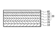
- a magnetic recording medium of one configuration example of the present invention includes a substrate, a first seed layer containing Ru, a second seed layer containing ZnO, a third seed layer containing MgO, and a magnetic recording layer containing an ordered alloy. Are included in this order.
- the magnetic recording medium of this configuration example may further include an orientation control layer between the substrate and the first seed layer.
- the magnetic recording medium of this configuration example may further include a nonmagnetic intermediate layer made of Pt between the first seed layer and the second seed layer.
- the magnetic recording medium of the present configuration example has a technology such as an adhesion layer, a soft magnetic backing layer, and / or a heat sink layer between the substrate and the first seed layer or between the substrate and the orientation control layer.
- FIG. 1 shows one configuration example of a magnetic recording medium including a substrate 10, an orientation control layer 20, a first seed layer 31, a second seed layer 32, a third seed layer 33, and a magnetic recording layer 40.
- the substrate 10 may be various plate-like members having a smooth surface.
- the substrate 10 can be formed using a material generally used for magnetic recording media. Materials that can be used include Al alloys plated with NiP, MgO single crystals, MgAl 2 O 4 , SrTiO 3 , tempered glass, crystallized glass and the like.
- An adhesion layer (not shown) that may be optionally provided is used to enhance adhesion between a layer formed on the adhesion layer and a layer formed below the adhesion layer.
- the layer formed under the adhesion layer includes the substrate 10.
- the material for forming the adhesion layer includes metals such as Ni, W, Ta, Cr, and Ru, and alloys containing the aforementioned metals.
- the adhesion layer may be a single layer or may have a laminated structure of a plurality of layers.
- a preferable adhesion layer in this configuration example is made of CrTi.
- a soft magnetic backing layer (not shown) that may be optionally provided controls the magnetic flux from the magnetic head to improve the recording / reproducing characteristics of the magnetic recording medium.
- Materials for forming the soft magnetic backing layer include NiFe alloys, Sendust (FeSiAl) alloys, crystalline materials such as CoFe alloys, microcrystalline materials such as FeTaC, CoFeNi, CoNiP, and Co alloys such as CoZrNb and CoTaZr. Includes amorphous material.
- the optimum value of the thickness of the soft magnetic underlayer depends on the structure and characteristics of the magnetic head used for magnetic recording. When the soft magnetic backing layer is formed by continuous film formation with other layers, it is preferable that the soft magnetic backing layer has a thickness in the range of 10 nm to 500 nm (including both ends) from the viewpoint of productivity.
- a heat sink layer may be provided.
- the heat sink layer is a layer for effectively absorbing excess heat of the magnetic recording layer 40 generated during the heat-assisted magnetic recording.
- the heat sink layer can be formed using a material having high thermal conductivity and specific heat capacity.
- a material includes Cu simple substance, Ag simple substance, Au simple substance, or an alloy material mainly composed of them.
- “mainly” means that the content of the material is 50% by mass or more.
- the heat sink layer can be formed using an Al—Si alloy, a Cu—B alloy, or the like.
- the heat sink layer can be formed using Sendust (FeSiAl) alloy, soft magnetic CoFe alloy, or the like.
- Sendust FeSiAl
- soft magnetic CoFe alloy By using the soft magnetic material, the function of concentrating the perpendicular magnetic field generated by the head on the magnetic recording layer 40 can be imparted to the heat sink layer, and the function of the soft magnetic backing layer can be supplemented.
- the optimum value of the heat sink layer thickness varies depending on the amount of heat and heat distribution during heat-assisted magnetic recording, the layer configuration of the magnetic recording medium, and the thickness of each component layer. In the case of forming by continuous film formation with other constituent layers, the film thickness of the heat sink layer is preferably 10 nm or more and 100 nm or less in consideration of productivity.
- the heat sink layer can be formed using any method known in the art, such as a sputtering method or a vacuum evaporation method. Usually, the heat sink layer is formed using a sputtering method.
- the heat sink layer can be provided between the substrate 10 and the adhesion layer, between the adhesion layer and the orientation control layer 20 in consideration of characteristics required for the magnetic recording medium.
- the orientation control layer 20 is a layer for forming a (002) -oriented hcp structure in the first seed layer 31 including Ru formed above.
- the orientation control layer 20 may be a single layer or may have a stacked structure of a plurality of layers.
- the orientation control layer 20 can be formed using a material used for a layer formed under a layer containing Ru in a magnetic recording medium having a magnetic recording layer containing a CoCrPt-based magnetic alloy of the prior art. This is described in, for example, Japanese Patent Application Laid-Open No. 2009-134797 (Patent Document 6).
- the material that can be used for forming the orientation control layer 20 is preferably a material having an hcp structure or a face-centered cubic (fcc) structure that is the same crystal structure as the magnetic recording layer, but is not limited thereto. is not.
- materials that can be used to form the orientation control layer 20 include Co—Ni alloys, Ni alloys, Pt alloys, Pd alloys, Ta alloys, Cr alloys, Si alloys, and Cu alloys.
- the material further includes one or more elements selected from the group consisting of Ru, W, Mo, Ta, Nb, and Ti. May be included.
- the material further includes one or more materials selected from the group consisting of B, Mn, Al, Si oxide, and Ti oxide. May be included.
- the preferred orientation control layer 20 is made of a RuCr alloy containing 50 atomic% or more of Ru.
- the RuCr alloy may contain a magnetic metal such as Fe, Ni or Co in an amount of less than 10 atomic%.
- a preferred orientation control layer 20 in this configuration example has a laminated structure of a NiTaAl alloy layer and a RuCrFe alloy layer.
- the orientation control layer 20 can be formed using any method known in the art such as sputtering.
- the first seed layer 31 includes Ru or a Ru alloy.
- the first seed layer 31 is made of Ru.
- the Ru and Ru alloy constituting the first seed layer 31 may contain inevitable impurities.
- the first seed layer 31 has a (002) -oriented hcp structure.
- the first seed layer 31 can be formed using any method known in the art such as sputtering.
- a nonmagnetic intermediate layer (not shown) that may optionally be provided between the first seed layer 31 and the second seed layer 32 is formed after the second seed layer 32 and the second seed layer 32. This is a layer for promoting the epitaxial growth of the layer.
- the nonmagnetic intermediate layer can be formed using Pt.
- the nonmagnetic intermediate layer can be formed using any method known in the art such as sputtering.
- the second seed layer 32 contains ZnO.
- ZnO may have a stoichiometric composition or a non-stoichiometric composition.
- ZnO in the second seed layer 32 has a (002) -oriented hexagonal close-packed structure, more specifically, a (002) -oriented wurtzite crystal structure.
- the compound group which has a peak is included.
- the second seed layer 32 is considered to have an effect of inducing the (002) orientation of the third seed layer 33 containing MgO and, as a result, inducing the (001) orientation of the magnetic recording layer 40. Further, it is considered that the second seed layer 32 containing ZnO has an effect of reducing the crystal orientation dispersion of the third seed layer 33 by having a small surface roughness.
- the second seed layer 32 preferably has a thickness in the range of 1 nm to 20 nm.
- the second seed layer 32 preferably contains 70% by mass or more of ZnO based on the total mass of the second seed layer 32.
- the third seed layer 33 contains MgO.
- MgO may have a stoichiometric composition or a non-stoichiometric composition.
- MgO in the third seed layer 33 has a (002) -oriented sodium chloride crystal structure.
- the third seed layer 33 induces the (001) orientation of the magnetic recording layer 40 formed thereon, and as a result, the crystal orientation dispersion of the magnetic recording layer 40 is reduced.
- the third seed layer 33 is considered to promote the separation of the magnetic crystal grains in the magnetic recording layer 40.
- the third seed layer 33 preferably has a thickness in the range of 1 nm to 20 nm.
- the third seed layer 33 preferably contains 70% by mass or more of MgO based on the total mass of the third seed layer 33.
- the second seed layer 32 and the third seed layer 33 can be formed using any method known in the art such as sputtering.
- the surface roughness of the third seed layer 33 containing MgO can be reduced by heating the substrate.
- the substrate temperature is preferably set within a range of 300 ° C to 500 ° C.
- the second seed layer 32 containing ZnO it is not necessary to heat the substrate during formation.
- the second seed layer 32 formed without heating the substrate can achieve a surface roughness equal to or lower than that of the third seed layer 33 formed with substrate heating.
- the first seed layer 31 described above by using the seed layer 30 of the laminated structure including the second seed layer 32 and the third seed layer, the ordered alloy in the magnetic recording layer 40, the crystal orientation of the particular L1 0 type ordered alloy Therefore, it is possible to obtain a (001) orientation suitable for the perpendicular magnetic recording medium.
- the magnetic recording layer 40 includes an ordered alloy.
- the ordered alloy includes at least one first element selected from the group consisting of Fe and Co, and at least one second element selected from the group consisting of Pt, Pd, Au, Ir, and Rh. .
- Preferred ordered alloy is FePt, CoPt, FePd, and L1 0 type ordered alloy selected from the group consisting of CoPd.
- the ordered alloy may further include at least one element selected from the group consisting of Ni, Mn, Cu, Ru, Ag, Au, and Cr. Desirable property modulation includes a decrease in temperature required for ordering of the ordered alloy and a decrease in heating temperature during recording by heat-assisted magnetic recording due to a decrease in Curie temperature.
- the ratio of the first element to the second element may be within the range of 0.7 to 1.3, preferably within the range of 0.8 to 1.1, based on the number of atoms. Good. By using the composition ratio within this range, it is possible to obtain L1 0 ordered structure having a large magnetic anisotropy constant Ku.
- the magnetic recording layer 40 may have a granular structure including magnetic crystal grains and nonmagnetic crystal grain boundaries surrounding the magnetic crystal grains.
- the magnetic crystal grain may include the ordered alloy described above.
- the nonmagnetic crystal grain boundary may include oxides such as SiO 2 , TiO 2 , and ZnO, nitrides such as SiN and TiN, and nonmagnetic materials such as carbon (C) and boron (B).
- the magnetic recording layer 40 may be composed of a plurality of magnetic layers. Each of the plurality of magnetic layers may have a non-granular structure or a granular structure. Furthermore, an ECC (Exchange-coupled Composite) structure in which a coupling layer such as Ru is sandwiched between magnetic layers may be provided. Further, the second magnetic layer may be provided on the upper part of the magnetic layer having the granular structure as a continuous layer (CAP layer) not including the granular structure.
- ECC Exchange-coupled Composite
- the magnetic recording layer 40 can be formed by depositing a predetermined material by a sputtering method.
- a target including a material forming the ordered alloy can be used. More specifically, it is possible to use a target containing the elements constituting the ordered alloy described above at a predetermined ratio.
- the magnetic recording layer 40 may be formed by using a plurality of targets containing a single element and adjusting the power applied to each target to control the ratio of the elements.
- a target including a material that forms magnetic crystal grains and a material that forms nonmagnetic crystal grain boundaries in a predetermined ratio can be used.
- a magnetic crystal grain and a nonmagnetic crystal grain boundary are prepared by adjusting a power applied to each target using a target containing a material that forms a magnetic crystal grain and a target containing a material that forms a nonmagnetic crystal grain boundary.
- the magnetic recording layer 40 may be formed by controlling the constituent ratio of the above.
- a plurality of targets separately containing elements constituting the ordered alloy may be used.
- the substrate is heated when the magnetic recording layer 40 is formed.
- the substrate temperature at this time is in the range of 300 ° C. to 600 ° C.
- a protective layer (not shown) which may be optionally provided can be formed using a material conventionally used in the field of magnetic recording media.
- the protective layer can be formed using a non-magnetic metal such as Pt, a carbon-based material such as diamond-like carbon, or a silicon-based material such as silicon nitride.
- the protective layer may be a single layer or may have a laminated structure of a plurality of layers.
- the protective layer having a stacked structure may be, for example, a stacked structure of two types of carbon-based materials having different characteristics, a stacked structure of a metal and a carbon-based material, or a stacked structure of a metal oxide film and a carbon-based material.
- the protective layer can be formed using any method known in the art, such as sputtering, CVD, and vacuum deposition.
- a liquid lubricant layer (not shown) which may be optionally provided can be formed using a material conventionally used in the field of magnetic recording media.
- a perfluoropolyether lubricant can be used.
- the liquid lubricant layer can be formed using, for example, a coating method such as a dip coating method or a spin coating method.
- Example 1 This embodiment relates to a magnetic recording medium having a seed layer 30 having a three-layer structure including a Ru first seed layer 31, a ZnO second seed layer 32, and an MgO third seed layer 33.
- a chemically strengthened glass substrate N-10 glass substrate manufactured by HOYA
- a 15 nm-thick CrTi adhesion layer was formed by DC magnetron sputtering using a CrTi target in Ar gas at a pressure of 0.3 Pa.
- the substrate temperature when forming the CrTi adhesion layer was room temperature (25 ° C.).
- the sputtering power when forming the CrTi adhesion layer was 200 W.
- a 4 nm thick NiTaAl film was formed by DC magnetron sputtering using a NiTaAl target in Ar gas at a pressure of 0.3 Pa.
- the substrate temperature when forming the NiTaAl film was room temperature (25 ° C.).
- the sputtering power when forming the NiTaAl film was 200 W.
- a RuCrFe film having a film thickness of 3.5 nm was formed by DC magnetron sputtering using an RuCrFe target in an Ar gas having a pressure of 0.3 Pa to obtain an orientation control layer 20 including a NiTaAl film and a RuCrFe film.
- the substrate temperature when forming the RuCrFe film was room temperature (25 ° C.).
- the sputtering power when forming the RuCrFe film was 200 W.
- a Ru first seed layer 31 having a film thickness of 6 nm was formed by a DC magnetron sputtering method using a Ru target in Ar gas at a pressure of 0.3 Pa.
- the substrate temperature when forming the Ru first seed layer 31 was room temperature (25 ° C.).
- the sputtering power when forming the Ru first seed layer 31 was 200 W.
- a ZnO second seed layer 32 having a thickness of 2 nm was formed by RF magnetron sputtering using a ZnO target in Ar gas at a pressure of 0.3 Pa.
- the substrate temperature when forming the ZnO second seed layer 32 was room temperature (25 ° C.).
- the sputtering power when forming the ZnO second seed layer 32 was 200 W.
- an MgO third seed layer 33 having a film thickness of 5 nm was formed by RF magnetron sputtering using an MgO target in Ar gas at a pressure of 0.016 Pa.
- the substrate temperature when forming the MgO third seed layer 33 was 400 ° C.
- the sputtering power when forming the MgO third seed layer 33 was 200 W.
- a 10 nm-thick FePt magnetic recording layer 40 was formed on the MgO third seed layer 33 by DC magnetron sputtering using an Fe target and a Pt target in Ar gas at a pressure of 1.0 Pa.
- the substrate temperature when forming the FePt magnetic recording layer 40 was set to 400 ° C. Further, 50 W of power was applied to the Fe target, and 17 W of power was applied to the Pt target.
- a Pt film having a film thickness of 5 nm was formed by DC magnetron sputtering using a Pt target in Ar gas at a pressure of 0.3 Pa.
- a Ta film having a film thickness of 5 nm is formed by DC magnetron sputtering using a Ta target in Ar gas at a pressure of 0.3 Pa, and a protective layer having a laminated structure of a Pt film and a Ta film is formed.
- a recording medium was obtained.
- the substrate temperature during the formation of the Pt film and the Ta film was room temperature (25 ° C.).
- the sputtering power when forming the Pt film was 50 W, and the sputtering power when forming the Ta film was 200 W.
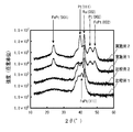
- the obtained magnetic recording medium was analyzed by X-ray diffraction (XRD), and the (001) FePt peak, (002) FePt peak, (111) FePt peak, and Pt nonmagnetic intermediate layer due to the FePt magnetic recording layer 40 were observed. The presence or absence of the (111) Pt peak and (002) Pt peak due to the occurrence, and the (002) Ru peak due to the Ru first seed layer were confirmed.
- the XRD spectrum of the obtained magnetic recording medium is shown in FIG.
- Example 2 This embodiment relates to a magnetic recording medium having a seed layer 30 having a four-layer structure including a Ru first seed layer 31, a nonmagnetic intermediate layer, a ZnO second seed layer 32, and an MgO third seed layer 33.
- the layers up to the Ru first seed layer 31 were formed by the same procedure as in Example 1.
- a Pt nonmagnetic intermediate layer having a thickness of 10 nm was formed by DC magnetron sputtering using a Pt target in Ar gas at a pressure of 0.3 Pa.
- the substrate temperature at the time of forming the Pt nonmagnetic intermediate layer was room temperature (25 ° C.).
- the sputtering power when forming the Pt nonmagnetic intermediate layer was 200 W.
- the ZnO second seed layer 32, the MgO third seed layer 33, the FePt magnetic recording layer 40, and the protective layer were formed to obtain a magnetic recording medium.
- the XRD spectrum of the obtained magnetic recording medium is shown in FIG.
- This embodiment relates to a magnetic recording medium that has only the Ru first seed layer 31 and does not have the ZnO second seed layer 32 and the MgO third seed layer 33.
- a magnetic recording medium was formed by the same procedure as in Example 1 except that the ZnO second seed layer 32 and the MgO third seed layer 33 were not formed.
- the XRD spectrum of the obtained magnetic recording medium is shown in FIG.
- the present embodiment relates to a magnetic recording medium having a Ru first seed layer 31 and a MgO third seed layer 33 and not having a ZnO second seed layer 32.
- a magnetic recording medium was formed by the same procedure as in Example 1 except that the ZnO second seed layer 32 was not formed.
- the XRD spectrum of the obtained magnetic recording medium is shown in FIG.
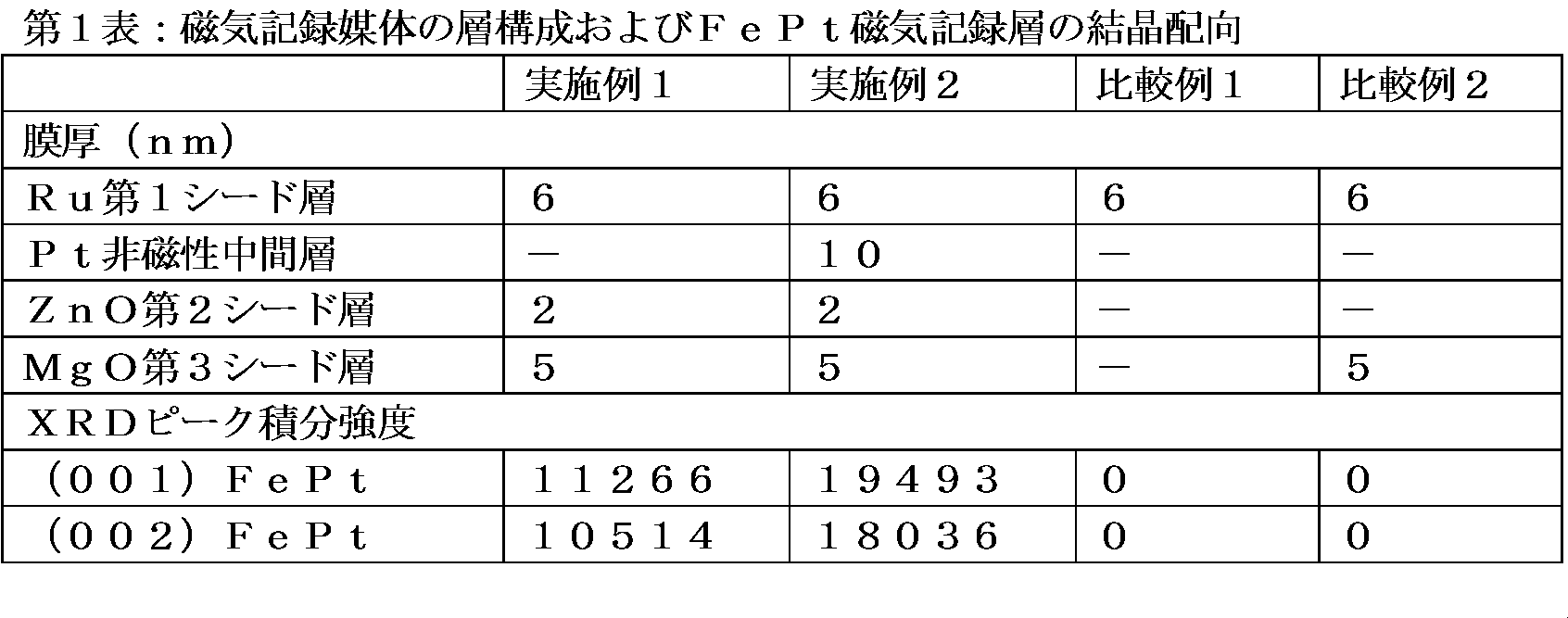
- Table 1 shows the integrated intensities of the (001) FePt peak and the (002) FePt peak obtained by XRD for the magnetic recording media of Examples 1 and 2 and Comparative Examples 1 and 2.
- the Pt nonmagnetic intermediate layer is formed of Pt having a (111) -oriented fcc structure.
- the magnetic recording medium of Example 2 showed a larger integrated intensity than the magnetic recording medium of Example 1 for both the (001) FePt peak and the (002) FePt peak. From this, it was found that the presence of the Pt nonmagnetic intermediate layer promotes the epitaxial growth of the FePt magnetic recording layer and provides a FePt magnetic recording layer having a more desirable crystal structure.
Landscapes
- Chemical & Material Sciences (AREA)
- Engineering & Computer Science (AREA)
- Materials Engineering (AREA)
- Chemical Kinetics & Catalysis (AREA)
- General Chemical & Material Sciences (AREA)
- Geochemistry & Mineralogy (AREA)
- Life Sciences & Earth Sciences (AREA)
- Organic Chemistry (AREA)
- Physics & Mathematics (AREA)
- Spectroscopy & Molecular Physics (AREA)
- Metallurgy (AREA)
- Magnetic Record Carriers (AREA)
- Inorganic Chemistry (AREA)
Abstract
Description
本実施例は、Ru第1シード層31、ZnO第2シード層32、およびMgO第3シード層33からなる3層構造のシード層30を有する磁気記録媒体に関する。最初に、平滑な表面を有する化学強化ガラス基板(HOYA社製N-10ガラス基板)を洗浄し、基板10を準備した。洗浄後の基板10を、インライン式のスパッタ装置内に導入した。圧力0.3PaのArガス中でCrTiターゲットを用いたDCマグネトロンスパッタ法により、膜厚15nmのCrTi密着層を形成した。CrTi密着層形成時の基板温度は室温(25℃)であった。CrTi密着層形成時のスパッタ電力は200Wであった。
本実施例は、Ru第1シード層31、非磁性中間層、ZnO第2シード層32、およびMgO第3シード層33からなる4層構造のシード層30を有する磁気記録媒体に関する。
本実施例は、Ru第1シード層31のみを有し、ZnO第2シード層32およびMgO第3シード層33を有さない磁気記録媒体に関する。ZnO第2シード層32およびMgO第3シード層33を形成しなかったことを除いて実施例1と同様の手順により、磁気記録媒体を形成した。得られた磁気記録媒体のXRDスペクトルを図2に示した。
本実施例は、Ru第1シード層31およびMgO第3シード層33を有し、ZnO第2シード層32を有さない磁気記録媒体に関する。ZnO第2シード層32を形成しなかったことを除いて実施例1と同様の手順により、磁気記録媒体を形成した。得られた磁気記録媒体のXRDスペクトルを図2に示した。
実施例1および2、ならびに比較例1および2の磁気記録媒体について、XRDにより得られた(001)FePtピークおよび(002)FePtピークの積分強度を第1表に示した。
20 配向制御層
30 シード層
31 第1シード層
32 第2シード層
33 第3シード層
40 磁気記録層
Claims (9)
- 基板と、Ruを含む第1シード層と、ZnOを含む第2シード層と、MgOを含む第3シード層と、規則合金を含む磁気記録層とをこの順に含むことを特徴とする磁気記録媒体。
- 前記第1シード層は、(002)配向した六方最密充填構造を有することを特徴とする請求項1に記載の磁気記録媒体。
- 前記基板と前記第1シード層との間に、配向制御層をさらに含むことを特徴とする請求項1に記載の磁気記録媒体。
- 前記第1シード層と前記第2シード層との間に、Ptからなる非磁性中間層をさらに含むことを特徴とする請求項1に記載の磁気記録媒体。
- 前記規則合金は、FeおよびCoから選択される少なくとも1種の元素と、Pt、Pd、Au、IrおよびRhからなる群から選択される少なくとも1種の元素とを含むL10型規則合金であることを特徴とする請求項1に記載の磁気記録媒体。
- 前記規則合金は、Ni、Mn、Cu、Ru、Ag、Au、およびCrからなる群から選択される少なくとも1種の元素をさらに含むことを特徴とする請求項5に記載の磁気記録媒体。
- 前記規則合金は、FePt、CoPt、FePd、およびCoPdからなる群から選択されるL10型規則合金であることを特徴とする請求項5に記載の磁気記録媒体。
- 前記磁気記録層が、磁性結晶粒と、前記磁性結晶粒を包囲する非磁性結晶粒界とを含むグラニュラー構造を有し、前記磁性結晶粒は前記規則合金を含むことを特徴とする請求項1に記載の磁気記録媒体。
- 前記非磁性結晶粒界は、炭素、ホウ素、酸化物、および窒化物からなる群から選択される非磁性材料を含むことを特徴とする請求項8に記載の磁気記録媒体。
Priority Applications (5)
| Application Number | Priority Date | Filing Date | Title |
|---|---|---|---|
| JP2017561594A JP6406462B2 (ja) | 2016-01-12 | 2017-01-05 | 磁気記録媒体 |
| SG11201710822TA SG11201710822TA (en) | 2016-01-12 | 2017-01-05 | Magnetic recording medium |
| CN201780002195.5A CN107735835B (zh) | 2016-01-12 | 2017-01-05 | 磁记录介质 |
| MYPI2017705041A MY181803A (en) | 2016-01-12 | 2017-01-05 | Magnetic recording medium |
| US15/856,036 US10847181B2 (en) | 2016-01-12 | 2017-12-27 | Magnetic recording medium |
Applications Claiming Priority (2)
| Application Number | Priority Date | Filing Date | Title |
|---|---|---|---|
| JP2016003577 | 2016-01-12 | ||
| JP2016-003577 | 2016-01-12 |
Related Child Applications (1)
| Application Number | Title | Priority Date | Filing Date |
|---|---|---|---|
| US15/856,036 Continuation US10847181B2 (en) | 2016-01-12 | 2017-12-27 | Magnetic recording medium |
Publications (1)
| Publication Number | Publication Date |
|---|---|
| WO2017122575A1 true WO2017122575A1 (ja) | 2017-07-20 |
Family
ID=59312119
Family Applications (1)
| Application Number | Title | Priority Date | Filing Date |
|---|---|---|---|
| PCT/JP2017/000160 Ceased WO2017122575A1 (ja) | 2016-01-12 | 2017-01-05 | 磁気記録媒体 |
Country Status (6)
| Country | Link |
|---|---|
| US (1) | US10847181B2 (ja) |
| JP (1) | JP6406462B2 (ja) |
| CN (1) | CN107735835B (ja) |
| MY (1) | MY181803A (ja) |
| SG (1) | SG11201710822TA (ja) |
| WO (1) | WO2017122575A1 (ja) |
Families Citing this family (2)
| Publication number | Priority date | Publication date | Assignee | Title |
|---|---|---|---|---|
| CN111435703B (zh) * | 2019-01-14 | 2024-03-22 | 联华电子股份有限公司 | 磁隧穿结装置及其形成方法 |
| JP7388226B2 (ja) * | 2020-02-13 | 2023-11-29 | 株式会社レゾナック | 磁気記録媒体およびその製造方法ならびに磁気記憶装置 |
Citations (2)
| Publication number | Priority date | Publication date | Assignee | Title |
|---|---|---|---|---|
| JP2006155865A (ja) * | 2004-10-29 | 2006-06-15 | Ken Takahashi | 垂直磁気記録媒体および垂直磁気記録再生装置 |
| JP2015026411A (ja) * | 2013-07-26 | 2015-02-05 | 昭和電工株式会社 | 磁気記録媒体および磁気記憶装置 |
Family Cites Families (15)
| Publication number | Priority date | Publication date | Assignee | Title |
|---|---|---|---|---|
| US7158346B2 (en) * | 2003-12-23 | 2007-01-02 | Seagate Technology Llc | Heat assisted magnetic recording film including superparamagnetic nanoparticles dispersed in an antiferromagnetic or ferrimagnetic matrix |
| JP2005276365A (ja) * | 2004-03-25 | 2005-10-06 | Toshiba Corp | グラニュラ薄膜、垂直磁気記録媒体および磁気記録再生装置 |
| US7405011B2 (en) | 2004-06-30 | 2008-07-29 | Hitachi Global Storage Technologies Netherlands B.V. | Magnetic recording media for tilted recording |
| JP4975335B2 (ja) * | 2006-02-16 | 2012-07-11 | 株式会社東芝 | 磁気抵抗効果素子,磁気ヘッド,および磁気記録再生装置 |
| US8063459B2 (en) * | 2007-02-12 | 2011-11-22 | Avalanche Technologies, Inc. | Non-volatile magnetic memory element with graded layer |
| JP4993296B2 (ja) | 2007-11-29 | 2012-08-08 | 富士電機株式会社 | 垂直磁気記録媒体 |
| JP5561773B2 (ja) | 2010-06-29 | 2014-07-30 | 昭和電工株式会社 | 熱アシスト磁気記録媒体及び磁気記憶装置 |
| CA2814716A1 (en) * | 2010-10-15 | 2012-04-19 | The Regents Of The University Of Michigan | Materials for controlling the epitaxial growth of photoactive layers in photovoltaic devices |
| JP2012195027A (ja) | 2011-03-15 | 2012-10-11 | Toshiba Corp | 磁気記録媒体、その製造方法、及び磁気記録再生装置 |
| JP5613910B2 (ja) * | 2011-05-17 | 2014-10-29 | 三菱マテリアル株式会社 | Pzt強誘電体薄膜の製造方法 |
| CN103534757B (zh) * | 2011-05-17 | 2016-08-17 | 昭和电工株式会社 | 磁记录介质及其制造方法以及磁记录再生装置 |
| JP5444447B2 (ja) | 2012-12-21 | 2014-03-19 | 株式会社東芝 | 磁気記録媒体、その製造方法、及び磁気記録再生装置 |
| JP6199618B2 (ja) * | 2013-04-12 | 2017-09-20 | 昭和電工株式会社 | 磁気記録媒体、磁気記憶装置 |
| JP6145332B2 (ja) * | 2013-06-20 | 2017-06-07 | 昭和電工株式会社 | 磁気記録媒体、磁気記憶装置 |
| JP2015135713A (ja) | 2014-01-17 | 2015-07-27 | 株式会社東芝 | 垂直磁気記録媒体、その製造方法、及び磁気記録再生装置 |
-
2017
- 2017-01-05 MY MYPI2017705041A patent/MY181803A/en unknown
- 2017-01-05 JP JP2017561594A patent/JP6406462B2/ja active Active
- 2017-01-05 SG SG11201710822TA patent/SG11201710822TA/en unknown
- 2017-01-05 CN CN201780002195.5A patent/CN107735835B/zh active Active
- 2017-01-05 WO PCT/JP2017/000160 patent/WO2017122575A1/ja not_active Ceased
- 2017-12-27 US US15/856,036 patent/US10847181B2/en active Active
Patent Citations (2)
| Publication number | Priority date | Publication date | Assignee | Title |
|---|---|---|---|---|
| JP2006155865A (ja) * | 2004-10-29 | 2006-06-15 | Ken Takahashi | 垂直磁気記録媒体および垂直磁気記録再生装置 |
| JP2015026411A (ja) * | 2013-07-26 | 2015-02-05 | 昭和電工株式会社 | 磁気記録媒体および磁気記憶装置 |
Also Published As
| Publication number | Publication date |
|---|---|
| SG11201710822TA (en) | 2018-02-27 |
| US10847181B2 (en) | 2020-11-24 |
| JPWO2017122575A1 (ja) | 2018-04-12 |
| CN107735835B (zh) | 2019-09-27 |
| US20180122415A1 (en) | 2018-05-03 |
| CN107735835A (zh) | 2018-02-23 |
| JP6406462B2 (ja) | 2018-10-17 |
| MY181803A (en) | 2021-01-07 |
Similar Documents
| Publication | Publication Date | Title |
|---|---|---|
| JP6439869B2 (ja) | 磁気記録媒体の製造方法 | |
| JP5999290B2 (ja) | 磁気記録媒体 | |
| JP6274305B2 (ja) | 磁気記録媒体 | |
| US10714138B2 (en) | Perpendicular magnetic recording medium | |
| CN104685566A (zh) | 磁记录介质 | |
| JPWO2015111384A1 (ja) | 垂直磁気記録媒体 | |
| JP6304468B2 (ja) | 磁気記録媒体およびこれを製造する方法 | |
| JP6406462B2 (ja) | 磁気記録媒体 | |
| JP6787433B2 (ja) | 磁気記録媒体 | |
| JP6327357B2 (ja) | 磁気記録媒体 | |
| JP6358640B2 (ja) | 磁気記録媒体 | |
| JP6304371B2 (ja) | 磁気記録媒体の製造方法 | |
| JP2015001996A (ja) | 磁気記録媒体 | |
| US10741207B2 (en) | Magnetic recording medium having an FePtRh magnetic layer | |
| WO2016079916A1 (ja) | 磁気記録媒体およびその製造方法 | |
| JP6354508B2 (ja) | 垂直磁気記録媒体 |
Legal Events
| Date | Code | Title | Description |
|---|---|---|---|
| 121 | Ep: the epo has been informed by wipo that ep was designated in this application |
Ref document number: 17738330 Country of ref document: EP Kind code of ref document: A1 |
|
| ENP | Entry into the national phase |
Ref document number: 2017561594 Country of ref document: JP Kind code of ref document: A |
|
| WWE | Wipo information: entry into national phase |
Ref document number: 11201710822T Country of ref document: SG |
|
| NENP | Non-entry into the national phase |
Ref country code: DE |
|
| 122 | Ep: pct application non-entry in european phase |
Ref document number: 17738330 Country of ref document: EP Kind code of ref document: A1 |