WO2017104669A1 - 熱硬化性接着シート、及び半導体装置の製造方法 - Google Patents
熱硬化性接着シート、及び半導体装置の製造方法 Download PDFInfo
- Publication number
- WO2017104669A1 WO2017104669A1 PCT/JP2016/087089 JP2016087089W WO2017104669A1 WO 2017104669 A1 WO2017104669 A1 WO 2017104669A1 JP 2016087089 W JP2016087089 W JP 2016087089W WO 2017104669 A1 WO2017104669 A1 WO 2017104669A1
- Authority
- WO
- WIPO (PCT)
- Prior art keywords
- acrylate
- meth
- resin component
- thermosetting adhesive
- adhesive sheet
- Prior art date
- Legal status (The legal status is an assumption and is not a legal conclusion. Google has not performed a legal analysis and makes no representation as to the accuracy of the status listed.)
- Ceased
Links
Images





Classifications
-
- C—CHEMISTRY; METALLURGY
- C09—DYES; PAINTS; POLISHES; NATURAL RESINS; ADHESIVES; COMPOSITIONS NOT OTHERWISE PROVIDED FOR; APPLICATIONS OF MATERIALS NOT OTHERWISE PROVIDED FOR
- C09J—ADHESIVES; NON-MECHANICAL ASPECTS OF ADHESIVE PROCESSES IN GENERAL; ADHESIVE PROCESSES NOT PROVIDED FOR ELSEWHERE; USE OF MATERIALS AS ADHESIVES
- C09J133/00—Adhesives based on homopolymers or copolymers of compounds having one or more unsaturated aliphatic radicals, each having only one carbon-to-carbon double bond, and at least one being terminated by only one carboxyl radical, or of salts, anhydrides, esters, amides, imides, or nitriles thereof; Adhesives based on derivatives of such polymers
- C09J133/04—Homopolymers or copolymers of esters
- C09J133/06—Homopolymers or copolymers of esters of esters containing only carbon, hydrogen and oxygen, the oxygen atom being present only as part of the carboxyl radical
- C09J133/08—Homopolymers or copolymers of acrylic acid esters
-
- C—CHEMISTRY; METALLURGY
- C09—DYES; PAINTS; POLISHES; NATURAL RESINS; ADHESIVES; COMPOSITIONS NOT OTHERWISE PROVIDED FOR; APPLICATIONS OF MATERIALS NOT OTHERWISE PROVIDED FOR
- C09J—ADHESIVES; NON-MECHANICAL ASPECTS OF ADHESIVE PROCESSES IN GENERAL; ADHESIVE PROCESSES NOT PROVIDED FOR ELSEWHERE; USE OF MATERIALS AS ADHESIVES
- C09J7/00—Adhesives in the form of films or foils
- C09J7/10—Adhesives in the form of films or foils without carriers
-
- C—CHEMISTRY; METALLURGY
- C09—DYES; PAINTS; POLISHES; NATURAL RESINS; ADHESIVES; COMPOSITIONS NOT OTHERWISE PROVIDED FOR; APPLICATIONS OF MATERIALS NOT OTHERWISE PROVIDED FOR
- C09J—ADHESIVES; NON-MECHANICAL ASPECTS OF ADHESIVE PROCESSES IN GENERAL; ADHESIVE PROCESSES NOT PROVIDED FOR ELSEWHERE; USE OF MATERIALS AS ADHESIVES
- C09J11/00—Features of adhesives not provided for in group C09J9/00, e.g. additives
- C09J11/02—Non-macromolecular additives
- C09J11/04—Non-macromolecular additives inorganic
-
- C—CHEMISTRY; METALLURGY
- C09—DYES; PAINTS; POLISHES; NATURAL RESINS; ADHESIVES; COMPOSITIONS NOT OTHERWISE PROVIDED FOR; APPLICATIONS OF MATERIALS NOT OTHERWISE PROVIDED FOR
- C09J—ADHESIVES; NON-MECHANICAL ASPECTS OF ADHESIVE PROCESSES IN GENERAL; ADHESIVE PROCESSES NOT PROVIDED FOR ELSEWHERE; USE OF MATERIALS AS ADHESIVES
- C09J11/00—Features of adhesives not provided for in group C09J9/00, e.g. additives
- C09J11/02—Non-macromolecular additives
- C09J11/06—Non-macromolecular additives organic
-
- C—CHEMISTRY; METALLURGY
- C09—DYES; PAINTS; POLISHES; NATURAL RESINS; ADHESIVES; COMPOSITIONS NOT OTHERWISE PROVIDED FOR; APPLICATIONS OF MATERIALS NOT OTHERWISE PROVIDED FOR
- C09J—ADHESIVES; NON-MECHANICAL ASPECTS OF ADHESIVE PROCESSES IN GENERAL; ADHESIVE PROCESSES NOT PROVIDED FOR ELSEWHERE; USE OF MATERIALS AS ADHESIVES
- C09J133/00—Adhesives based on homopolymers or copolymers of compounds having one or more unsaturated aliphatic radicals, each having only one carbon-to-carbon double bond, and at least one being terminated by only one carboxyl radical, or of salts, anhydrides, esters, amides, imides, or nitriles thereof; Adhesives based on derivatives of such polymers
- C09J133/04—Homopolymers or copolymers of esters
- C09J133/06—Homopolymers or copolymers of esters of esters containing only carbon, hydrogen and oxygen, the oxygen atom being present only as part of the carboxyl radical
- C09J133/10—Homopolymers or copolymers of methacrylic acid esters
-
- C—CHEMISTRY; METALLURGY
- C09—DYES; PAINTS; POLISHES; NATURAL RESINS; ADHESIVES; COMPOSITIONS NOT OTHERWISE PROVIDED FOR; APPLICATIONS OF MATERIALS NOT OTHERWISE PROVIDED FOR
- C09J—ADHESIVES; NON-MECHANICAL ASPECTS OF ADHESIVE PROCESSES IN GENERAL; ADHESIVE PROCESSES NOT PROVIDED FOR ELSEWHERE; USE OF MATERIALS AS ADHESIVES
- C09J7/00—Adhesives in the form of films or foils
-
- C—CHEMISTRY; METALLURGY
- C09—DYES; PAINTS; POLISHES; NATURAL RESINS; ADHESIVES; COMPOSITIONS NOT OTHERWISE PROVIDED FOR; APPLICATIONS OF MATERIALS NOT OTHERWISE PROVIDED FOR
- C09J—ADHESIVES; NON-MECHANICAL ASPECTS OF ADHESIVE PROCESSES IN GENERAL; ADHESIVE PROCESSES NOT PROVIDED FOR ELSEWHERE; USE OF MATERIALS AS ADHESIVES
- C09J7/00—Adhesives in the form of films or foils
- C09J7/30—Adhesives in the form of films or foils characterised by the adhesive composition
-
- H—ELECTRICITY
- H10—SEMICONDUCTOR DEVICES; ELECTRIC SOLID-STATE DEVICES NOT OTHERWISE PROVIDED FOR
- H10P—GENERIC PROCESSES OR APPARATUS FOR THE MANUFACTURE OR TREATMENT OF DEVICES COVERED BY CLASS H10
- H10P10/00—Bonding of wafers, substrates or parts of devices
- H10P10/12—Bonding of semiconductor wafers or semiconductor substrates to semiconductor wafers or semiconductor substrates
-
- H—ELECTRICITY
- H10—SEMICONDUCTOR DEVICES; ELECTRIC SOLID-STATE DEVICES NOT OTHERWISE PROVIDED FOR
- H10P—GENERIC PROCESSES OR APPARATUS FOR THE MANUFACTURE OR TREATMENT OF DEVICES COVERED BY CLASS H10
- H10P52/00—Grinding, lapping or polishing of wafers, substrates or parts of devices
-
- H—ELECTRICITY
- H10—SEMICONDUCTOR DEVICES; ELECTRIC SOLID-STATE DEVICES NOT OTHERWISE PROVIDED FOR
- H10P—GENERIC PROCESSES OR APPARATUS FOR THE MANUFACTURE OR TREATMENT OF DEVICES COVERED BY CLASS H10
- H10P54/00—Cutting or separating of wafers, substrates or parts of devices
-
- H—ELECTRICITY
- H10—SEMICONDUCTOR DEVICES; ELECTRIC SOLID-STATE DEVICES NOT OTHERWISE PROVIDED FOR
- H10P—GENERIC PROCESSES OR APPARATUS FOR THE MANUFACTURE OR TREATMENT OF DEVICES COVERED BY CLASS H10
- H10P72/00—Handling or holding of wafers, substrates or devices during manufacture or treatment thereof
- H10P72/70—Handling or holding of wafers, substrates or devices during manufacture or treatment thereof for supporting or gripping
- H10P72/74—Handling or holding of wafers, substrates or devices during manufacture or treatment thereof for supporting or gripping using temporarily an auxiliary support
- H10P72/7402—Wafer tapes, e.g. grinding or dicing support tapes
-
- C—CHEMISTRY; METALLURGY
- C08—ORGANIC MACROMOLECULAR COMPOUNDS; THEIR PREPARATION OR CHEMICAL WORKING-UP; COMPOSITIONS BASED THEREON
- C08K—Use of inorganic or non-macromolecular organic substances as compounding ingredients
- C08K3/00—Use of inorganic substances as compounding ingredients
- C08K3/01—Use of inorganic substances as compounding ingredients characterized by their specific function
- C08K3/013—Fillers, pigments or reinforcing additives
-
- C—CHEMISTRY; METALLURGY
- C09—DYES; PAINTS; POLISHES; NATURAL RESINS; ADHESIVES; COMPOSITIONS NOT OTHERWISE PROVIDED FOR; APPLICATIONS OF MATERIALS NOT OTHERWISE PROVIDED FOR
- C09J—ADHESIVES; NON-MECHANICAL ASPECTS OF ADHESIVE PROCESSES IN GENERAL; ADHESIVE PROCESSES NOT PROVIDED FOR ELSEWHERE; USE OF MATERIALS AS ADHESIVES
- C09J2203/00—Applications of adhesives in processes or use of adhesives in the form of films or foils
- C09J2203/326—Applications of adhesives in processes or use of adhesives in the form of films or foils for bonding electronic components such as wafers, chips or semiconductors
-
- C—CHEMISTRY; METALLURGY
- C09—DYES; PAINTS; POLISHES; NATURAL RESINS; ADHESIVES; COMPOSITIONS NOT OTHERWISE PROVIDED FOR; APPLICATIONS OF MATERIALS NOT OTHERWISE PROVIDED FOR
- C09J—ADHESIVES; NON-MECHANICAL ASPECTS OF ADHESIVE PROCESSES IN GENERAL; ADHESIVE PROCESSES NOT PROVIDED FOR ELSEWHERE; USE OF MATERIALS AS ADHESIVES
- C09J2301/00—Additional features of adhesives in the form of films or foils
- C09J2301/40—Additional features of adhesives in the form of films or foils characterized by the presence of essential components
- C09J2301/408—Additional features of adhesives in the form of films or foils characterized by the presence of essential components additives as essential feature of the adhesive layer
-
- C—CHEMISTRY; METALLURGY
- C09—DYES; PAINTS; POLISHES; NATURAL RESINS; ADHESIVES; COMPOSITIONS NOT OTHERWISE PROVIDED FOR; APPLICATIONS OF MATERIALS NOT OTHERWISE PROVIDED FOR
- C09J—ADHESIVES; NON-MECHANICAL ASPECTS OF ADHESIVE PROCESSES IN GENERAL; ADHESIVE PROCESSES NOT PROVIDED FOR ELSEWHERE; USE OF MATERIALS AS ADHESIVES
- C09J2433/00—Presence of (meth)acrylic polymer
-
- H—ELECTRICITY
- H10—SEMICONDUCTOR DEVICES; ELECTRIC SOLID-STATE DEVICES NOT OTHERWISE PROVIDED FOR
- H10P—GENERIC PROCESSES OR APPARATUS FOR THE MANUFACTURE OR TREATMENT OF DEVICES COVERED BY CLASS H10
- H10P72/00—Handling or holding of wafers, substrates or devices during manufacture or treatment thereof
- H10P72/70—Handling or holding of wafers, substrates or devices during manufacture or treatment thereof for supporting or gripping
- H10P72/74—Handling or holding of wafers, substrates or devices during manufacture or treatment thereof for supporting or gripping using temporarily an auxiliary support
- H10P72/7416—Handling or holding of wafers, substrates or devices during manufacture or treatment thereof for supporting or gripping using temporarily an auxiliary support used during dicing or grinding
-
- H—ELECTRICITY
- H10—SEMICONDUCTOR DEVICES; ELECTRIC SOLID-STATE DEVICES NOT OTHERWISE PROVIDED FOR
- H10P—GENERIC PROCESSES OR APPARATUS FOR THE MANUFACTURE OR TREATMENT OF DEVICES COVERED BY CLASS H10
- H10P72/00—Handling or holding of wafers, substrates or devices during manufacture or treatment thereof
- H10P72/70—Handling or holding of wafers, substrates or devices during manufacture or treatment thereof for supporting or gripping
- H10P72/74—Handling or holding of wafers, substrates or devices during manufacture or treatment thereof for supporting or gripping using temporarily an auxiliary support
- H10P72/744—Details of chemical or physical process used for separating the auxiliary support from a device or a wafer
-
- H—ELECTRICITY
- H10—SEMICONDUCTOR DEVICES; ELECTRIC SOLID-STATE DEVICES NOT OTHERWISE PROVIDED FOR
- H10W—GENERIC PACKAGES, INTERCONNECTIONS, CONNECTORS OR OTHER CONSTRUCTIONAL DETAILS OF DEVICES COVERED BY CLASS H10
- H10W72/00—Interconnections or connectors in packages
- H10W72/01—Manufacture or treatment
- H10W72/012—Manufacture or treatment of bump connectors, dummy bumps or thermal bumps
-
- H—ELECTRICITY
- H10—SEMICONDUCTOR DEVICES; ELECTRIC SOLID-STATE DEVICES NOT OTHERWISE PROVIDED FOR
- H10W—GENERIC PACKAGES, INTERCONNECTIONS, CONNECTORS OR OTHER CONSTRUCTIONAL DETAILS OF DEVICES COVERED BY CLASS H10
- H10W72/00—Interconnections or connectors in packages
- H10W72/071—Connecting or disconnecting
- H10W72/072—Connecting or disconnecting of bump connectors
-
- H—ELECTRICITY
- H10—SEMICONDUCTOR DEVICES; ELECTRIC SOLID-STATE DEVICES NOT OTHERWISE PROVIDED FOR
- H10W—GENERIC PACKAGES, INTERCONNECTIONS, CONNECTORS OR OTHER CONSTRUCTIONAL DETAILS OF DEVICES COVERED BY CLASS H10
- H10W72/00—Interconnections or connectors in packages
- H10W72/20—Bump connectors, e.g. solder bumps or copper pillars; Dummy bumps; Thermal bumps
- H10W72/241—Dispositions, e.g. layouts
Definitions
- the present invention relates to a thermosetting adhesive sheet for reinforcing a semiconductor wafer and a method for manufacturing a semiconductor device in order to prevent cracks during the dicing process.
- the dicing (individualization) process gives a great stress to the semiconductor wafer. For this reason, cracks called chipping occur in the semiconductor wafer, and the defect rate may increase.
- thermosetting adhesive sheet that reinforces the semiconductor wafer immediately before the dicing process (after back grinding) (see, for example, Patent Document 1).
- thermosetting adhesive sheet capable of reducing warpage of a semiconductor wafer and occurrence of chipping
- a method for manufacturing a semiconductor device I will provide a.
- thermosetting adhesive sheet is a thermosetting formed from a resin composition containing (meth) acrylate, a resin component containing a polymerization initiator, and a filler.
- the (meth) acrylate includes a solid (meth) acrylate and a tri- or higher functional (meth) acrylate, and the content of the solid (meth) acrylate in the resin component is 55 wt%.
- the sum of the values obtained by multiplying the number of functional groups per unit molecular weight of (meth) acrylate by the content of (meth) acrylate in the resin component is 2.7E-03 or more, and The blending amount is 80 to 220 parts by mass with respect to 100 parts by mass of the resin component.
- the method for manufacturing a semiconductor device includes a grinding process for polishing a semiconductor wafer, a thermosetting adhesive sheet attaching process for attaching a thermosetting adhesive sheet to the polished surface of the semiconductor wafer, and the thermosetting Curing process for curing the sheet and reducing the amount of warpage of the semiconductor wafer, a dicing tape attaching process for attaching a dicing tape to the thermosetting adhesive sheet surface of the semiconductor wafer, and a dicing process for the wafer with the dicing tape attached And a dicing process step for obtaining individual semiconductor chips, wherein the thermosetting adhesive sheet comprises a resin component containing (meth) acrylate, a polymerization initiator, and a filler.
- thermosetting adhesive layer It has a formed thermosetting adhesive layer, and the (meth) acrylate is solid (meth) acrylate and trifunctional or higher (meta).
- the content of solid (meth) acrylate in the resin component is 55 wt% or more, and the number of functional groups per unit molecular weight of the (meth) acrylate is the number of functional groups in the resin component.
- the sum of the values multiplied by the content is 2.7E-03 or more, and the blending amount of the filler is 80 to 220 parts by mass with respect to 100 parts by mass of the resin component.
- thermosetting adhesive sheet contracts and the warp of the semiconductor wafer can be reduced by bonding the thermosetting adhesive sheet to the polished surface of the semiconductor wafer and curing it. For this reason, dicing can be performed with the wafer flattened, so that chipping can be reduced and a high-quality semiconductor device can be obtained.
- FIG. 1 is a cross-sectional view schematically showing a thermosetting adhesive sheet.
- FIG. 2 is a cross-sectional view showing an outline of the BG tape attaching step.
- FIG. 3 is a cross-sectional view showing an outline of a grinding process.
- FIG. 4 is a cross-sectional view showing an outline of a thermosetting adhesive sheet attaching step.
- FIG. 5 is a cross-sectional view schematically showing the BG tape peeling step.
- FIG. 6 is a cross-sectional view schematically showing the curing process.
- FIG. 7 is a cross-sectional view showing an outline of the DC tape attaching step.
- FIG. 8 is a cross-sectional view schematically showing the dicing process.
- FIG. 9 is a cross-sectional view showing an outline of the expanding process.
- FIG. 10 is a cross-sectional view schematically showing the pickup process.
- FIG. 11 is a cross-sectional view schematically showing the mounting process.
- thermosetting adhesive sheet has a thermosetting adhesive layer that is bonded to the polishing surface of the semiconductor wafer when dicing the semiconductor wafer and reinforces the wafer during the dicing process, which is called chipping. This is a reinforcing sheet for preventing cracks.
- FIG. 1 is a cross-sectional view showing an outline of a thermosetting adhesive sheet. As shown in FIG. 1, the thermosetting adhesive sheet has a base film layer 11 and a thermosetting adhesive layer 12 laminated.
- a porous substrate made of a plastic film such as polyethylene terephthalate, polyethylene, polypropylene, or polyester, paper, cloth, nonwoven fabric, or the like can be used.
- the thermosetting adhesive layer 12 is formed of a resin composition containing a resin component containing (meth) acrylate, a polymerization initiator, and a filler.
- (meth) acrylate is meant to include acrylic acid ester (acrylate) and methacrylic acid ester (methacrylate).
- (meth) acrylate monofunctional (meth) acrylate, bifunctional (meth) acrylate, trifunctional or higher (meth) acrylate can be used.
- Examples of monofunctional (meth) acrylates include polyalkylene glycol ester monomers and alkyl (meth) acrylates having a linear or branched alkyl group.
- Specific examples of the polyalkylene glycol ester monomer include, for example, hydroxyethyl (meth) acrylate, hydroxypropyl (meth) acrylate, 4-hydroxybutyl acrylate, polyethylene glycol mono (meth) acrylate, and polypropylene glycol mono (meth) acrylate.
- bifunctional (meth) acrylate examples include tricyclodecane dimethanol di (meth) acrylate, dimethylol-tricyclodecane di (meth) acrylate, bisphenol AEO-modified di (meth) acrylate, 1,9-nonanediol di ( (Meth) acrylate, 1,10-decandiol di (meth) acrylate, 2-hydroxy-3-acryloyloxypropyl (meth) acrylate, propoxylated bisphenol A di (meth) acrylate, diethylene glycol di (meth) acrylate, neopentyl Glycol di (meth) acrylate, 1,4-butanediol di (meth) acrylate, polyethylene glycol (200) di (meth) acrylate, tetraethylene glycol di (meth) acrylate, polyethylene glycol Cole (400) di (meth) acrylate, cyclohexanedimethanol di (meth)
- tricyclodecane dimethanol di (meth) acrylate can be preferably used from the viewpoints of reactivity and crosslinkability.
- bifunctional (meth) acrylate available on the market include the trade name “A-DCP” (tricyclodecane dimethanol diacrylate) of Shin-Nakamura Chemical Co., Ltd.
- Trifunctional or higher functional (meth) acrylates include isocyanuric acid EO-modified tri (meth) acrylate, dipentaerythritol hexa (meth) acrylate, pentaerythritol tri (meth) acrylate, and EO-modified pentaerythritol tri (meth).
- isocyanuric acid EO-modified triacrylate and dipentaerythritol hexaacrylate can be preferably used from the viewpoints of reactivity and crosslinkability.
- Specific examples of trifunctional or higher functional (meth) acrylates available on the market include the trade name “M-315” (a mixture of isocyanuric acid ethylene oxide-modified diacrylate and isocyanuric acid ethylene oxide-modified triacrylate) manufactured by Toagosei Co., Ltd.
- solid (meth) acrylate and trifunctional or higher functional (meth) acrylate are used as (meth) acrylate.
- solid (meth) acrylate is solid (meth) acrylate in normal temperature (25 degreeC), and if it says from a viewpoint of melting
- Examples of the solid (meth) acrylate include those having a high molecular weight such as epoxy (meth) acrylate and urethane (meth) acrylate, and those having high crystallinity and a melting point of 50 ° C. or less are preferable.
- Epoxy (meth) acrylate can be obtained, for example, by reacting an epoxy resin with a vinyl group-containing monocarboxylic acid.
- Examples of the epoxy resin include novolac type epoxy resin, bisphenol A type epoxy resin, and bisphenol F type epoxy resin.
- Examples of the vinyl group-containing monocarboxylic acid include (meth) acrylic acid and (meth) acrylic acid.
- Examples thereof include ⁇ -furfuryl (meth) acrylic acid, ⁇ -styryl (meth) acrylic acid, and cinnamic acid.
- bisphenol-type epoxy (meth) acrylate obtained by reacting bisphenol A-type phenoxy resin or bisphenol F-type phenoxy resin with (meth) acrylic acid can be preferably used.
- Specific examples of the solid bisphenol type epoxy (meth) acrylate available on the market include trade names “VR-90” and “VR-60” of Showa High Polymer Co., Ltd.
- the weight average molecular weight of the solid (meth) acrylate is preferably 500 to 10,000, more preferably 800 to 3000.
- the weight average molecular weight is 500 or more, the film property tends to be improved, and when it is 10,000 or less, the tack property tends to be improved.
- the content of solid (meth) acrylate in the resin component is 55 wt% or more, preferably 60 wt% or more, more preferably 70 wt% or more.
- the warpage controllability of the wafer tends to be improved.
- the (meth) acrylate has a (meth) acryloyl group having two or more functional groups, if the molecular weight is remarkably large with respect to the number of functional groups, the property tends to approximate that of the monofunctional acrylate, and the warpage of the wafer Controllability is reduced. For this reason, it is preferable to select the polyfunctional (meth) acrylate in consideration of the “functional number per unit molecular weight” obtained by dividing the functional number by the molecular weight.
- the average crosslink density which is the sum of values obtained by multiplying the number of functional groups per unit molecular weight by the content of (meth) acrylate in the resin component, is a predetermined value or more, and thus thermosetting adhesion.
- the shrinkage rate of the layer becomes large, and it becomes possible to cancel the warpage of the wafer.
- the total sum of values obtained by multiplying the number of functional groups per unit molecular weight of (meth) acrylate by the content of (meth) acrylate in the resin component is 2.7E-03 or more.
- the upper limit of the sum of the values obtained by multiplying the number of functional groups per unit molecular weight of (meth) acrylate by the content of (meth) acrylate in the resin component is preferably 5.0E-02 or less. More preferably, it is 0E-02 or less. If the average crosslinking density is too small, it becomes difficult to cancel the warpage of the semiconductor wafer, and if it is too large, characteristics such as adhesion to the semiconductor wafer tend to deteriorate.
- the content of (meth) acrylate in the resin component is preferably 85 wt% or more, more preferably 90 wt% or more. If the content of the (meth) acrylate in the resin component is too small, it becomes difficult to cancel the warp of the semiconductor wafer, and if it is too large, the sheet characteristics tend to deteriorate.
- the weight average molecular weight of (meth) acrylate is preferably 100 to 100,000, more preferably 200 to 50,000. If the weight average molecular weight is too small or too large, the warpage controllability of the wafer tends to be lowered.
- an organic peroxide that is an initiator of a radical reaction can be used as the polymerization initiator.
- the one minute half-life temperature of the organic peroxide is preferably 130 ° C. or lower, more preferably 80 ° C. or higher and 120 ° C. or lower. If the half-life temperature for 1 minute is too large, it is difficult to obtain a large reaction rate, and if it is too small, the room temperature storage property tends to be lowered.
- organic peroxides examples include dilauroyl peroxide (1 minute half-life temperature: 116.4 ° C.), dibenzoyl peroxide (1 minute half-life temperature: 130.0 ° C.), di (4- Methylbenzoyl) peroxide (1 minute half-life temperature: 128.2 ° C), 1,1,3,3-tetramethylbutylperoxy-2-ethylhexanoate (1 minute half-life temperature: 124.3 ° C) Di (3,5,5-trimethylhexanoyl) peroxide (1 minute half-life temperature: 112.6 ° C.), t-butyl peroxypivalate (1 minute half-life temperature: 110.3 ° C.), t- Hexyl peroxypivalate (1 minute half-life temperature: 109.1 ° C), t-butyl peroxyneoheptanoate (1 minute half-life temperature: 104.6 ° C), t-butyl peroxy Odecanoate (1 minute half-life temperature: 11
- dilauroyl peroxide and 1,1,3,3-tetramethylbutylperoxy-2-ethylhexanoate can be preferably used from the viewpoint of reactivity and crosslinkability.
- Specific examples of dilauroyl peroxide available on the market include “Paroyl L”, a trade name of NOF Corporation.
- the content of the organic peroxide is preferably 0.1 parts by mass or more and 20 parts by mass or less, and more preferably 1 part by mass or more and 10 parts by mass or less with respect to 80 parts by mass of (meth) acrylate. preferable. If the content of the organic peroxide is too small, the reactivity decreases, and if it is too large, the product life tends to decrease.
- the resin component may include a polymer such as an elastomer or a phenoxy resin.
- elastomer examples include acrylic elastomers, butadiene elastomers, ethylene elastomers, propylene elastomers, and styrene elastomers, and one or more of these can be used. Among these, it is preferable to use an acrylic elastomer having excellent transparency. Specific examples of the acrylic elastomer available on the market include “SG-P3”, a trade name of Nagase ChemteX Corporation.
- phenoxy resin examples include a fluorene type phenoxy resin, a bisphenol type phenoxy resin, a novolac type phenoxy resin, a naphthalene type phenoxy resin, a biphenyl type phenoxy resin, and the like. One or more of these may be used. it can.
- the weight average molecular weight (Mw) of the polymer is preferably 5000 or more and 150,000 or less, more preferably 10,000 or more and 80000 or less. If the weight average molecular weight (Mw) is too small, the sheet characteristics tend to deteriorate, and if too large, the compatibility with other components tends to deteriorate.
- the content of the polymer in the resin component is preferably 15 wt% or less, more preferably 5% or less.
- the warp controllability of the wafer tends to decrease.
- silane coupling agent As the silane coupling agent, (meth) acrylic, epoxy-based, amino-based, mercapto-based, sulfide-based, ureido-based and the like can be used. In this embodiment, the (meth) acrylic-based silane coupling agent is used. Is preferably used. Thereby, the adhesion reliability in the interface of an organic material and an inorganic material can be improved.
- the filler either inorganic or organic can be used, and it is preferable to use a material having transparency to infrared rays used in alignment.
- the material having transparency to infrared rays include silica, silicon, germanium, quartz, sapphire, and the like, and one or more of these can be used. Among these, it is preferable to use silica from the viewpoint of laser mark visibility.
- the blending amount of the filler is 80 to 220 parts by mass with respect to 100 parts by mass of the resin component, and preferably 80 to 180 parts by mass. If the filler content is too small, the effect of reducing the amount of warpage of the wafer tends to be reduced, and if too much, the adhesion reliability tends to be reduced.
- a colorant such as a black pigment as another filler.
- the colorant causes a contrast difference between the laser marking portion and other portions, and improves the laser mark visibility.
- examples of such a colorant include carbon black, titanium black, titanium oxide, iron oxide, and the like, and one or more of these can be used. Among these, it is preferable to use carbon black from the viewpoint of improving the contrast difference.
- the transmittance of the thermosetting adhesive sheet at a wavelength of 1000 nm is preferably 30% or more. If the infrared transmittance is too low, it is difficult to perform alignment using infrared rays.
- thermosetting adhesive sheet shrinks by being bonded to the polished surface of the semiconductor wafer and cured, and the warpage of the semiconductor wafer can be reduced. For this reason, dicing can be performed with the wafer flattened, so that chipping can be reduced and a high-quality semiconductor device can be obtained.
- the method for manufacturing a semiconductor device includes a grinding process for polishing a semiconductor wafer, a process for bonding a thermosetting adhesive sheet to the polishing surface of the semiconductor wafer and curing the semiconductor wafer, and reducing the amount of warpage of the semiconductor wafer. And a dicing process in which a dicing tape is bonded to the thermosetting adhesive sheet surface of the semiconductor wafer and diced. Since warping of the semiconductor wafer is reduced and dicing is possible with the wafer flattened, chipping can be reduced and a high-quality semiconductor device can be obtained.
- the manufacturing method of the semiconductor device shown as a specific example includes a protective tape attaching step (A) for applying a protective tape having an adhesive layer, a grinding step (B), a thermosetting resin sheet attaching step (C), and a protection Tape peeling step (D), curing step (E), adhesive tape attaching step (F), dicing step (G), expanding step (H), pick-up step (I), and mounting step (J ).
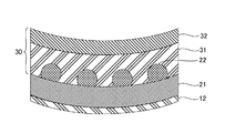
- FIG. 2 is a cross-sectional view showing an outline of the protective tape attaching step.
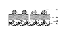
- the protective tape 30 is attached to the surface of the wafer 21 on which the protruding electrodes 22 are formed.
- Affixing temperature for applying the protective tape 30 is 25 ° C. or higher and 100 ° C. or lower, preferably 40 ° C. or higher and 80 ° C. or lower, from the viewpoint of reducing voids, improving wafer adhesion and preventing warpage after wafer grinding.
- the wafer 21 has an integrated circuit formed on a semiconductor surface such as silicon, and a protruding electrode 22 for connection called a bump.
- the thickness of the wafer 21 is not particularly limited, but is preferably 200 ⁇ m or more and 1000 ⁇ m or less.
- the protruding electrode 22 is not particularly limited, and examples thereof include a low melting point bump or a high melting point bump made of solder, a tin bump, a silver-tin bump, a silver-tin-copper bump, a gold bump, and a copper bump.
- the height of the protruding electrode 22 is not particularly limited, but is preferably 10 ⁇ m or more and 200 ⁇ m or less.
- the protective tape 30 is called a back grind tape, and protects the wafer from scratches, cracks, contamination, etc. in the next grinding process (B).
- the protective tape 30 is formed by laminating a thermoplastic resin layer 31 and a base film layer 32, and bonding them so that the formation surface of the protruding electrode 22 and the thermoplastic resin layer 31 are in contact with each other.
- the electrode 22 is embedded in the thermoplastic resin layer 31.
- thermoplastic resin layer 31 ethylene vinyl acetate copolymer (EVA), polyethylene, polypropylene, polyamide, polyacetal, polyethylene terephthalate, polybutylene terephthalate, fluororesin, polyphenylene sulfide, polystyrene, ABS resin, acrylic type Resins, polycarbonates, polyurethanes, polyvinyl chlorides, polyphenylene oxides and the like may be mentioned. These may be used alone or in combination of two or more.
- EVA ethylene vinyl acetate copolymer
- a plastic substrate such as polyethylene terephthalate, polyethylene, polypropylene, polyester, or a porous substrate made of paper, cloth, nonwoven fabric, or the like can be used.
- the protective tape 30 is not limited to the above-described configuration, and other layers may be formed on the surface of each layer or between adjacent layers.
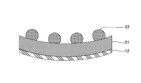
- FIG. 3 is a cross-sectional view showing an outline of a grinding process.
- the surface opposite to the surface to which the protective tape 30 is applied is ground.
- the opposite surface of the wafer 21 to which the protective tape 30 is attached is fixed to a grinding device for polishing.
- the thickness of the wafer 21 by polishing is 200 ⁇ m or less, and further 50 ⁇ m or less.
- the warpage amount of the wafer 21 is the maximum value of the warpage (Z axis) when the wafer 21 is placed on the flat stage (X, Y axes).
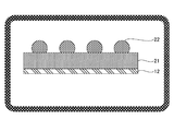
- FIG. 4 is a cross-sectional view showing an outline of a thermosetting adhesive sheet attaching step.
- the thermosetting adhesive layer 12 of the thermosetting adhesive sheet is attached to the grind treated surface of the wafer 21.
- FIG. 5 is a cross-sectional view schematically showing the protective tape peeling step.
- the protective tape 30 is peeled off.
- FIG. 6 is a cross-sectional view schematically showing the curing process.
- the thermosetting adhesive layer 12 is cured.
- a known method for curing a thermosetting adhesive can be used.
- the thermosetting adhesive layer 12 can be cured by curing at a temperature of 80 to 180 ° C. for a time of 0.1 to 5 hours.
- the thermosetting adhesive layer 12 is greatly contracted, and stress in a direction opposite to the warp of the wafer 21 is generated, so that the wafer 21 can be maintained in a flat state.
- FIG. 7 is a cross-sectional view schematically showing the adhesive tape attaching step.
- the adhesive tape 40 is applied to the grinding surface.
- the adhesive tape 40 is called a dicing tape, and is a tape for protecting and fixing the wafer 21 in the dicing process (G) and holding it until the pickup process (I).
- the adhesive tape 40 is not particularly limited, and a known tape can be used.
- the adhesive tape 40 has an adhesive layer and a base film layer.
- the pressure-sensitive adhesive layer include polyethylene-based, acrylic-based, rubber-based, and urethane-based pressure-sensitive adhesives.
- the porous base material which consists of plastic films, such as a polyethylene terephthalate, polyethylene, a polypropylene, polyester, paper, cloth, a nonwoven fabric, etc. can be used.
- it does not specifically limit as an adhesive tape sticking apparatus and conditions A well-known apparatus and conditions are used.
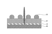
- FIG. 8 is a cross-sectional view schematically showing the dicing process.
- the wafer 21 with the adhesive tape 40 attached is diced to obtain individual semiconductor chips.
- the dicing method is not particularly limited, and a known method such as cutting the wafer 21 with a dicing saw can be used. Since the thermosetting adhesive sheet reduces the warpage of the wafer, dicing can be performed with the wafer flattened, and chipping can be reduced.
- FIG. 9 is a cross-sectional view showing an outline of the expanding process.
- the adhesive tape 40 to which a plurality of divided semiconductor chips are attached is elongated in the radial direction to widen the intervals between the individual semiconductor chips.
- FIG. 10 is a cross-sectional view schematically showing the pickup process.
- the semiconductor chip adhered and fixed on the adhesive tape 40 is pushed up from the lower surface of the adhesive tape 40 and peeled off, and the peeled semiconductor chip is adsorbed by a collet.
- the picked-up semiconductor chip is stored in a chip tray or conveyed to a chip mounting nozzle of a flip chip bonder.
- FIG. 11 is a cross-sectional view schematically showing the mounting process.
- the semiconductor chip and the circuit board are connected using a circuit connection material such as NCF (Non Conductive Film).
- NCF Non Conductive Film
- plastic substrates such as a polyimide substrate and a glass epoxy substrate, a ceramic substrate, etc. can be used.
- connection method the well-known method using a heating bonder, a reflow furnace, etc. can be used.
- thermosetting adhesive sheet is bonded to the polishing surface of the semiconductor wafer and cured, and the amount of warpage of the semiconductor wafer is reduced, so that chipping is suppressed and dicing is easily performed. be able to.
- thermosetting adhesive sheet was prepared, and this was bonded to a patterned wafer in which warpage occurred, thereby preparing a laminate. And the film film property of a thermosetting adhesive sheet, the chipping suppression at the time of dicing, and the controllability of the curvature of a wafer were evaluated.
- thermosetting adhesive sheet The following components were blended to prepare a resin composition. This was applied to peeled PET (Polyethylene terephthalate) using a bar coater and dried in an oven at 80 ° C. for 3 minutes to produce a thermosetting adhesive sheet having a thermosetting adhesive layer having a thickness of 20 ⁇ m ( Cover peeling PET (25 ⁇ m) / thermosetting adhesive layer (20 ⁇ m) / base peeling PET (50 ⁇ m)).
- VR-90 Bisphenol A type epoxy acrylate (Showa High Polymer Co., Ltd., number of functional groups per unit molecular weight (functional group / molecular
- thermosetting adhesive layer having a thickness of 20 ⁇ m was bonded onto the patterned wafer with a press and cured under conditions of 130 ° C. and 1 h to obtain a laminate.
- the 8-inch wafer with a thickness of 200 ⁇ m was used as the patterned wafer. Further, the average warpage amount (number of samples: 10) of the patterned wafer was 4 mm. The warpage amount of the patterned wafer was the maximum value of the warpage (Z axis) when the patterned wafer was placed on the flat stage (X, Y axes).
- the warpage amount of the laminated body was set to the maximum value of the warpage (Z axis) when the laminated body was placed on the planar stage (X, Y axes). 1. “A” when the warp amount of the laminate is less than 1.0 mm, “B” when the warp amount of the laminate is 1.0 mm or more and less than 1.5 mm, and 1.5 mm or more. Those having a thickness of less than 5 mm were evaluated as “C”, and those having a warped amount of 2.5 mm or more were evaluated as “D”.
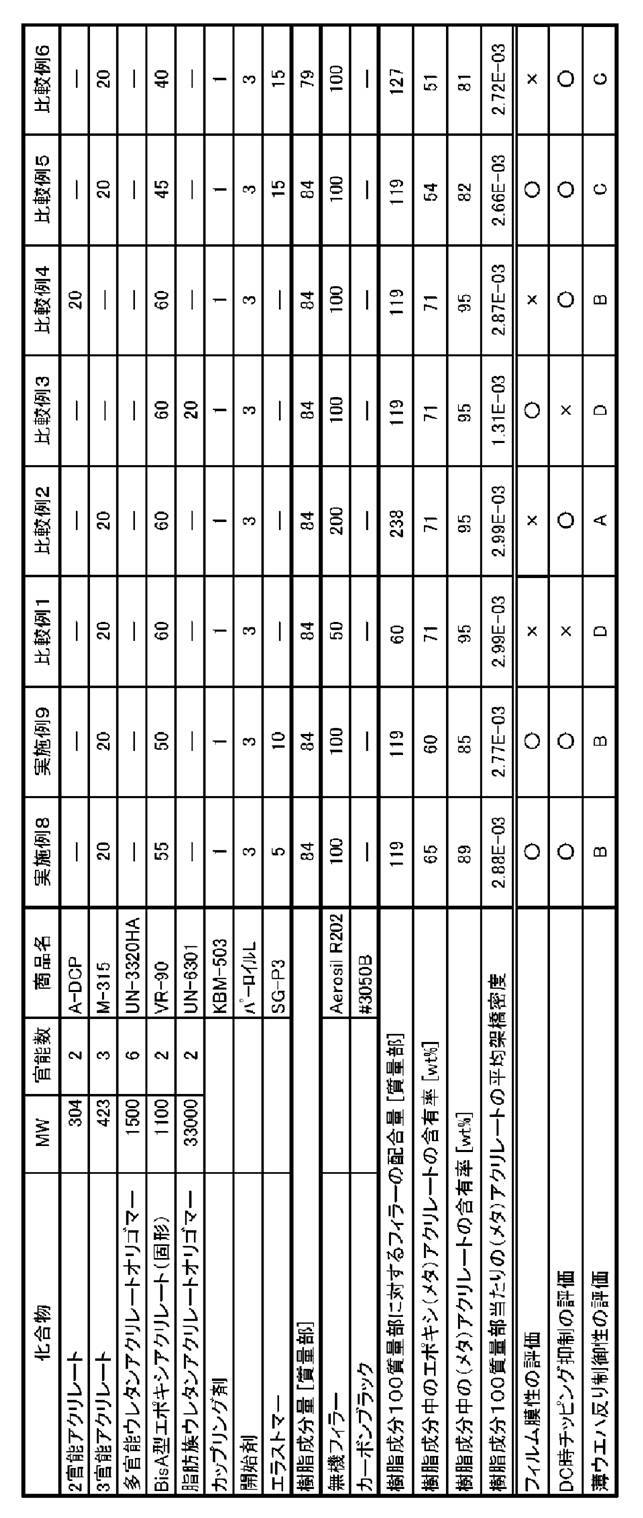
- Example 1 As shown in Table 1, 20 parts by mass of trifunctional acrylate (M-315), 60 parts by mass of bisphenol A type epoxy acrylate (VR-90), 1 part by mass of coupling agent (KBM-503), A resin composition was prepared by adding 100 parts by mass of an inorganic filler (Aerosil R202) to 84 parts by mass of a resin component containing 3 parts by mass of an oxide (Perroyl L).
- M-315 trifunctional acrylate
- VR-90 bisphenol A type epoxy acrylate
- KBM-503 1 part by mass of coupling agent
- the blending amount of the inorganic filler with respect to 100 parts by mass of the resin component is 119 parts by mass, the content of the solid (meth) acrylate in the resin component is 71 wt%, the content of the (meth) acrylate in the resin component is 95 wt%, (meth)
- the sum total of the values obtained by multiplying the number of functional groups per unit molecular weight of the acrylate by the content of the (meth) acrylate in the resin component was 2.99E-03. Evaluation of the film film property of the thermosetting adhesive sheet produced using this resin composition was ⁇ , evaluation of chipping suppression during dicing was ⁇ , and evaluation of thin wafer warpage controllability was A.
- Example 2 As shown in Table 1, a resin composition was prepared in the same manner as in Example 1 except that 70 parts by mass of an inorganic filler (Aerosil R202) was added.
- the compounding amount of the inorganic filler with respect to 100 parts by mass of the resin component is 83 parts by mass, the solid (meth) acrylate content in the resin component is 71 wt%, the (meth) acrylate content in the resin component is 95 wt%, (meth)
- the sum total of the values obtained by multiplying the number of functional groups per unit molecular weight of the acrylate by the content of the (meth) acrylate in the resin component was 2.99E-03. Evaluation of the film film property of the thermosetting adhesive sheet produced using this resin composition was ⁇ , evaluation of chipping suppression during dicing was ⁇ , and evaluation of thin wafer warpage controllability was A.
- Example 3 As shown in Table 1, a resin composition was prepared in the same manner as in Example 1 except that 150 parts by mass of an inorganic filler (Aerosil R202) was added.
- the blending amount of the inorganic filler with respect to 100 parts by mass of the resin component is 179 parts by mass, the solid (meth) acrylate content in the resin component is 71 wt%, the (meth) acrylate content in the resin component is 95 wt%, (meth)
- the sum total of the values obtained by multiplying the number of functional groups per unit molecular weight of the acrylate by the content of the (meth) acrylate in the resin component was 2.99E-03. Evaluation of the film film property of the thermosetting adhesive sheet produced using this resin composition was ⁇ , evaluation of chipping suppression during dicing was ⁇ , and evaluation of thin wafer warpage controllability was A.
- Example 4 As shown in Table 1, a resin composition was prepared in the same manner as in Example 1 except that 15 parts by mass of trifunctional acrylate (M-315) and 5 parts by mass of polyfunctional urethane acrylate oligomer (UN-3320HA) were blended. did.
- the blending amount of the inorganic filler with respect to 100 parts by mass of the resin component is 119 parts by mass, the content of the solid (meth) acrylate in the resin component is 71 wt%, the content of the (meth) acrylate in the resin component is 95 wt%, (meth)
- the total sum of the values obtained by multiplying the number of functional groups per unit molecular weight of the acrylate by the content of the (meth) acrylate in the resin component was 2.80E-03. Evaluation of the film film property of the thermosetting adhesive sheet produced using this resin composition was ⁇ , evaluation of chipping suppression during dicing was ⁇ , and evaluation of thin wafer warpage controllability was A.
- Example 5 As shown in Table 1, a resin composition was prepared in the same manner as in Example 1 except that 17 parts by mass of trifunctional acrylate (M-315) and 3 parts by mass of aliphatic urethane acrylate oligomer (UN-6301) were blended. did.
- the blending amount of the inorganic filler with respect to 100 parts by mass of the resin component is 119 parts by mass, the content of the solid (meth) acrylate in the resin component is 71 wt%, the content of the (meth) acrylate in the resin component is 95 wt%, (meth)
- the total sum of values obtained by multiplying the number of functional groups per unit molecular weight of the acrylate by the content of (meth) acrylate in the resin component was 2.74E-03. Evaluation of the film film property of the thermosetting adhesive sheet produced using this resin composition was ⁇ , evaluation of chipping suppression during dicing was ⁇ , and evaluation of thin wafer warpage controllability was B.
- Example 6 As shown in Table 1, a resin composition was prepared in the same manner as in Example 1 except that 3 parts by mass of bifunctional acrylate (A-DCP) and 17 parts by mass of trifunctional acrylate (M-315) were blended.
- the blending amount of the inorganic filler with respect to 100 parts by mass of the resin component is 119 parts by mass, the content of the solid (meth) acrylate in the resin component is 71 wt%, the content of the (meth) acrylate in the resin component is 95 wt%, (meth)
- the total sum of the values obtained by multiplying the number of functional groups per unit molecular weight of the acrylate by the content of (meth) acrylate in the resin component was 2.97E-03. Evaluation of the film film property of the thermosetting adhesive sheet produced using this resin composition was ⁇ , evaluation of chipping suppression during dicing was ⁇ , and evaluation of thin wafer warpage controllability was B.
- Example 7 As shown in Table 1, a resin composition was prepared in the same manner as in Example 1 except that 5 parts by mass of carbon black was added.
- the blending amount of the inorganic filler with respect to 100 parts by mass of the resin component is 125 parts by mass, the content of solid (meth) acrylate in the resin component is 71 wt%, the content of (meth) acrylate in the resin component is 95 wt%, (meth)
- the sum total of the values obtained by multiplying the number of functional groups per unit molecular weight of the acrylate by the content of the (meth) acrylate in the resin component was 2.99E-03. Evaluation of the film film property of the thermosetting adhesive sheet produced using this resin composition was ⁇ , evaluation of chipping suppression during dicing was ⁇ , and evaluation of thin wafer warpage controllability was A.
- Example 8> As shown in Table 2, a resin composition was prepared in the same manner as in Example 1 except that 55 parts by mass of bisphenol A type epoxy acrylate (VR-90) and 5 parts by mass of elastomer (SG-P3) were blended.
- the blending amount of the inorganic filler with respect to 100 parts by mass of the resin component is 119 parts by mass
- the solid (meth) acrylate content in the resin component is 65 wt%
- the (meth) acrylate content in the resin component is 89 wt%
- (meth) The sum of values obtained by multiplying the number of functional groups per unit molecular weight of the acrylate by the content of (meth) acrylate in the resin component was 2.88E-03.
- Evaluation of the film film property of the thermosetting adhesive sheet produced using this resin composition was ⁇
- evaluation of chipping suppression during dicing was ⁇
- evaluation of thin wafer warpage controllability was B.
- Example 9 As shown in Table 2, a resin composition was prepared in the same manner as in Example 1 except that 50 parts by mass of bisphenol A type epoxy acrylate (VR-90) and 10 parts by mass of elastomer (SG-P3) were blended.
- the blending amount of the inorganic filler with respect to 100 parts by mass of the resin component is 119 parts by mass
- the solid (meth) acrylate content in the resin component is 60 wt%
- the (meth) acrylate content in the resin component is 85 wt%
- (meth) The sum of the values obtained by multiplying the number of functional groups per unit molecular weight of the acrylate by the content of the (meth) acrylate in the resin component was 2.77E-03.
- Evaluation of the film film property of the thermosetting adhesive sheet produced using this resin composition was ⁇
- evaluation of chipping suppression during dicing was ⁇
- evaluation of thin wafer warpage controllability was B.
- a resin composition was prepared in the same manner as in Example 1 except that 50 parts by mass of the inorganic filler was added.
- the blending amount of the inorganic filler with respect to 100 parts by mass of the resin component is 60 parts by mass, the content of solid (meth) acrylate in the resin component is 71 wt%, the content of (meth) acrylate in the resin component is 95 wt%, (meth)
- the sum total of the values obtained by multiplying the number of functional groups per unit molecular weight of the acrylate by the content of the (meth) acrylate in the resin component was 2.99E-03.
- the evaluation of the film film property of the thermosetting adhesive sheet produced using this resin composition was x, the evaluation of chipping suppression during dicing was x, and the evaluation of thin wafer warpage controllability was D.
- a resin composition was prepared in the same manner as in Example 1 except that 200 parts by mass of the inorganic filler was added.
- the compounding amount of the inorganic filler with respect to 100 parts by mass of the resin component is 238 parts by mass
- the content of solid (meth) acrylate in the resin component is 71 wt%
- the content of (meth) acrylate in the resin component is 95 wt%
- (meth) The sum total of the values obtained by multiplying the number of functional groups per unit molecular weight of the acrylate by the content of the (meth) acrylate in the resin component was 2.99E-03.
- Evaluation of the film film property of the thermosetting adhesive sheet produced using this resin composition was x
- evaluation of chipping suppression during dicing was ⁇
- evaluation of thin wafer warpage controllability was A.
- a resin composition was prepared in the same manner as in Example 1 except that 20 parts by mass of an aliphatic urethane acrylate oligomer (UN-6301) was used instead of the trifunctional acrylate.
- the blending amount of the inorganic filler with respect to 100 parts by mass of the resin component is 119 parts by mass, the content of the solid (meth) acrylate in the resin component is 71 wt%, the content of the (meth) acrylate in the resin component is 95 wt%, (meth)
- the total sum of values obtained by multiplying the number of functional groups per unit molecular weight of the acrylate by the content of the (meth) acrylate in the resin component was 1.31E-03.
- the evaluation of the film film property of the thermosetting adhesive sheet produced using this resin composition was ⁇ , the evaluation of chipping suppression during dicing was ⁇ , and the evaluation of thin wafer warpage controllability was D.
- a resin composition was prepared in the same manner as in Example 1 except that 20 parts by mass of bifunctional acrylate (A-DCP) was used instead of trifunctional acrylate.
- the blending amount of the inorganic filler with respect to 100 parts by mass of the resin component is 119 parts by mass, the content of the solid (meth) acrylate in the resin component is 71 wt%, the content of the (meth) acrylate in the resin component is 95 wt%, (meth)
- the sum of the values obtained by multiplying the number of functional groups per unit molecular weight of the acrylate by the content of (meth) acrylate in the resin component was 2.87E-03. Evaluation of the film film property of the thermosetting adhesive sheet produced using this resin composition was x, evaluation of chipping suppression during dicing was ⁇ , and evaluation of thin wafer warpage controllability was B.
- a resin composition was prepared in the same manner as in Example 1 except that 45 parts by mass of bisphenol A type epoxy acrylate (VR-90) and 15 parts by mass of elastomer (SG-P3) were blended.
- the blending amount of the inorganic filler with respect to 100 parts by mass of the resin component is 119 parts by mass
- the content of the solid (meth) acrylate in the resin component is 54 wt%
- the content of the (meth) acrylate in the resin component is 82 wt%
- (meth) The sum of the values obtained by multiplying the number of functional groups per unit molecular weight of the acrylate by the content of the (meth) acrylate in the resin component was 2.66E-03.
- Evaluation of the film film property of the thermosetting adhesive sheet produced using this resin composition was ⁇
- evaluation of chipping suppression during dicing was ⁇
- evaluation of thin wafer warpage controllability was C.
- a resin composition was prepared in the same manner as in Example 1 except that 40 parts by mass of bisphenol A type epoxy acrylate (VR-90) and 15 parts by mass of elastomer (SG-P3) were blended.
- the blending amount of the inorganic filler with respect to 100 parts by mass of the resin component is 127 parts by mass
- the solid (meth) acrylate content in the resin component is 51 wt%
- the (meth) acrylate content in the resin component is 81 wt%
- (meth) The total sum of values obtained by multiplying the number of functional groups per unit molecular weight of the acrylate by the content of the (meth) acrylate in the resin component was 2.72E-03.
- Evaluation of the film film property of the thermosetting adhesive sheet produced using this resin composition was x
- evaluation of chipping suppression during dicing was ⁇
- evaluation of thin wafer warpage controllability was C.
- thermosetting adhesive layer 11 base film layer, 12 thermosetting adhesive layer, 21 wafer, 22 protruding electrode, 30 protective tape, 31 thermoplastic resin layer, 32 base film layer
Landscapes
- Chemical & Material Sciences (AREA)
- Organic Chemistry (AREA)
- Inorganic Chemistry (AREA)
- Adhesives Or Adhesive Processes (AREA)
- Adhesive Tapes (AREA)
- Mechanical Treatment Of Semiconductor (AREA)
- Dicing (AREA)
Abstract
Description
1.熱硬化性接着シート
2.半導体装置の製造方法
3.実施例
本実施の形態に係る熱硬化性接着シートは、半導体ウエハをダイシングする際に、半導体ウエハの研磨面に貼り合わされる熱硬化性接着層を有し、ダイシング工程時にウエハを補強し、チッピングと呼ばれるクラックを防止する補強シートである。
次に、前述の熱硬化性接着シートを用いた半導体装置の製造方法について説明する。本実施の形態に係る半導体装置の製造方法は、半導体ウエハを研磨するグラインド工程と、半導体ウエハの研磨面に熱硬化性接着シートを貼り合わせて硬化させ、半導体ウエハの反り量を低減させる工程と、半導体ウエハの熱硬化性接着シート面にダイシングテープを貼り合わせ、ダイシングするダイシング工程とを有する。半導体ウエハの反りを低減させ、ウエハを平坦化させた状態でダイシングが可能となるため、チッピングを低減させ、高品質な半導体装置を得ることができる。
図2は、保護テープ貼付工程の概略を示す断面図である。保護テープ貼付工程では、突起電極22が形成されたウエハ21面に保護テープ30を貼り付ける。保護テープ30を貼り付ける貼付温度は、ボイドの減少、ウエハ密着性の向上およびウエハ研削後の反り防止の観点から、25℃以上100℃以下、好ましくは40℃以上80℃以下である。
図3は、グラインド工程の概略を示す断面図である。グラインド工程では、保護テープ30貼付面の反対面をグラインド処理する。保護テープ30を貼り付けたウエハ21の反対面を研削装置に固定して研磨する。このグラインド工程において、研磨によりウエハ21の厚さは、200μm以下、さらには50μm以下である。ウエハ21の厚さを小さくすればするほど、ウエハ21の反り量が大きくなる。なお、ウエハ21の反り量は、平面ステージ(X,Y軸)にウエハ21を置いたときの反り(Z軸)の最大値である。
図4は、熱硬化性接着シート貼付工程の概略を示す断面図である。熱硬化性接着シート貼付工程では、ウエハ21のグラインド処理面に熱硬化性接着シートの熱硬化性接着層12を貼付する。
図5は、保護テープ剥離工程の概略を示す断面図である。保護テープ剥離工程では、保護テープ30を剥離する。
図6は、硬化工程の概略を示す断面図である。硬化工程では、熱硬化性接着層12を硬化させる。硬化方法及び硬化条件としては、熱硬化型の接着剤を硬化させる公知の方法を用いることができる。硬化工程では、例えば、80~180℃の温度、0.1~5hの時間でキュアすることにより、熱硬化性接着層12を硬化させることが可能である。これにより、熱硬化性接着層12が大きく収縮し、ウエハ21の反りと逆方向の応力が生じるため、ウエハ21を平坦な状態に維持させることが可能となる。
図7は、粘着テープ貼付工程の概略を示す断面図である。粘着テープ貼付工程では、グラインド処理面に粘着テープ40を貼付する。粘着テープ40は、ダイシングテープ(Dicing Tape)と呼ばれるものであり、ダイシング工程(G)において、ウエハ21を保護、固定し、ピックアップ工程(I)まで保持するためのテープである。
図8は、ダイシング処理工程の概略を示す断面図である。ダイシング処理工程では、粘着テープ40が貼付されたウエハ21をダイシング処理し、個片の半導体チップを得る。ダイシング方法としては、特に限定されず、例えばダイシングソーでウエハ21を切削して切り出すなどの公知の方法を用いることができる。熱硬化性接着シートがウエハの反りを低減させているため、ウエハを平坦化させた状態でダイシングすることができ、チッピングを低減させることができる。
図9は、エキスパンド工程の概略を示す断面図である。エキスパンド工程では、例えば分割された複数個の半導体チップが貼着されている粘着テープ40を放射方向に伸長させ、個々の半導体チップの間隔を広げる。
図10は、ピックアップ工程の概略を示す断面図である。ピックアップ工程では、粘着テープ40上に貼着固定された半導体チップを、粘着テープ40の下面より突き上げて剥離させ、この剥離された半導体チップをコレットで吸着する。ピックアップされた半導体チップは、チップトレイに収納されるか、またはフリップチップボンダーのチップ搭載ノズルへと搬送される。
図11は、実装工程の概略を示す断面図である。実装工程では、例えば半導体チップと回路基板とをNCF(Non Conductive Film)などの回路接続材料を用いて接続する。回路基板としては、特に限定されないが、ポリイミド基板、ガラスエポキシ基板などのプラスチック基板、セラミック基板などを用いることができる。また、接続方法としては、加熱ボンダー、リフロー炉などを用いる公知の方法を用いることができる。
以下、本発明の実施例について説明する。本実施例では、熱硬化性接着シートを作製し、これを反りが発生したパターン付ウエハに貼り合わせ、積層体を作製した。そして、熱硬化性接着シートのフィルム膜性、ダイシング時のチッピング抑制、及びウエハの反りの制御性について評価した。
下記成分を配合し、樹脂組成物を調製した。これを、剥離処理されたPET(Polyethylene terephthalate)にバーコーターを用いて塗布し、80℃のオーブンで3分間乾燥させ、厚み20μmの熱硬化性接着層を有する熱硬化性接着シートを作製した(カバー剥離PET(25μm)/熱硬化性接着層(20μm)/ベース剥離PET(50μm))。
A-DCP:トリシクロデカンジメタノールジアクリレート(新中村化学工業(株)、単位分子量当たりの官能基数(官能基数/分子量)=0.0065)
M-315:イソシアヌル酸エチレンオキサイド変性ジアクリレートとイソシアヌル酸エチレンオキサイド変性トリアクリレートの混合物(イソシアヌル酸エチレンオキサイド 変性ジアクリレートの含有率が3%~13%)(東亞合成(株)、単位分子量当たりの官能基数(官能基数/分子量)=0.007)
UN-3320HA:多官能ウレタンアクリレートオリゴマー(根上工業(株)、単位分子量当たりの官能基数(官能基数/分子量)=0.004)
VR-90:ビスフェノールA型エポキシアクリレート(昭和高分子(株)、単位分子量当たりの官能基数(官能基数/分子量)=0.0018)
UN-6301:脂肪族ウレタンアクリレートオリゴマー(根上工業(株)、単位分子量当たりの官能基数(官能基数/分子量)=0.00006)
KBM-503:シランカップリング剤(信越シリコーン(株))
パーロイルL:ジラウロイルパーオキサイド(日油(株)製、1分間半減期温度:116.4℃)
SG-P3:エラストマー(ナガセケムテックス(株)製)
アエロジルR202:シリカ(日本アエロジル(株))
#3050B:カーボンブラック(三菱化学(株))
厚み20μmの熱硬化性接着層をパターン付ウエハ上にプレス機にて貼り合わせ、130℃、1hの条件でキュアして積層体を得た。
熱硬化性接着シートのフィルム性、タック性、及びラミネート性について評価し、全ての評価が良好である場合を「○」と評価し、いずれか1つの評価が不良である場合を「×」と評価した。
積層体の熱硬化性接着層側にダイシングテープをラミネートし、ダイシング後の積層体を観察した。チッピングによる不良率が5%未満である場合を「○」と評価し、不良率が5%以上である場合を「×」と評価した。
パターン付ウエハの反り量の測定と同様に、積層体の反り量は、平面ステージ(X,Y軸)に積層体を置いたときの反り(Z軸)の最大値とした。積層体の反り量が1.0mm未満のものを「A」、積層体の反り量が1.0mm以上1.5mm未満のものを「B」、積層体の反り量が1.5mm以上2.5mm未満のものを「C」、積層体の反り量が2.5mm以上のものを「D」と評価した。
表1に示すように、3官能アクリレート(M-315)を20質量部、ビスフェノールA型エポキシアクリレート(VR-90)を60質量部、カップリング剤(KBM-503)を1質量部、有機過酸化物(パーロイルL)を3質量部配合した樹脂成分84質量部に、無機フィラー(アエロジルR202)100質量部を添加して樹脂組成物を調製した。樹脂成分100質量部に対する無機フィラーの配合量は119質量部、樹脂成分中の固形(メタ)アクリレートの含有率は71wt%、樹脂成分中の(メタ)アクリレートの含有率は95wt%、(メタ)アクリレートの単位分子量当たりの官能基数に、樹脂成分中の(メタ)アクリレートの含有率を乗じた値の総和は2.99E-03であった。この樹脂組成物を用いて作製した熱硬化性接着シートのフィルム膜性の評価は○、ダイシング時のチッピング抑制の評価は○、薄ウエハ反り制御性の評価はAであった。
表1に示すように、無機フィラー(アエロジルR202)を70質量部添加した以外は、実施例1と同様に樹脂組成物を調製した。樹脂成分100質量部に対する無機フィラーの配合量は83質量部、樹脂成分中の固形(メタ)アクリレートの含有率は71wt%、樹脂成分中の(メタ)アクリレートの含有率は95wt%、(メタ)アクリレートの単位分子量当たりの官能基数に、樹脂成分中の(メタ)アクリレートの含有率を乗じた値の総和は2.99E-03であった。この樹脂組成物を用いて作製した熱硬化性接着シートのフィルム膜性の評価は○、ダイシング時のチッピング抑制の評価は○、薄ウエハ反り制御性の評価はAであった。
表1に示すように、無機フィラー(アエロジルR202)を150質量部添加した以外は、実施例1と同様に樹脂組成物を調製した。樹脂成分100質量部に対する無機フィラーの配合量は179質量部、樹脂成分中の固形(メタ)アクリレートの含有率は71wt%、樹脂成分中の(メタ)アクリレートの含有率は95wt%、(メタ)アクリレートの単位分子量当たりの官能基数に、樹脂成分中の(メタ)アクリレートの含有率を乗じた値の総和は2.99E-03であった。この樹脂組成物を用いて作製した熱硬化性接着シートのフィルム膜性の評価は○、ダイシング時のチッピング抑制の評価は○、薄ウエハ反り制御性の評価はAであった。
表1に示すように、3官能アクリレート(M-315)を15質量部、多官能ウレタンアクリレートオリゴマー(UN-3320HA)を5質量部配合した以外は、実施例1と同様に樹脂組成物を調製した。樹脂成分100質量部に対する無機フィラーの配合量は119質量部、樹脂成分中の固形(メタ)アクリレートの含有率は71wt%、樹脂成分中の(メタ)アクリレートの含有率は95wt%、(メタ)アクリレートの単位分子量当たりの官能基数に、樹脂成分中の(メタ)アクリレートの含有率を乗じた値の総和は2.80E-03であった。この樹脂組成物を用いて作製した熱硬化性接着シートのフィルム膜性の評価は○、ダイシング時のチッピング抑制の評価は○、薄ウエハ反り制御性の評価はAであった。
表1に示すように、3官能アクリレート(M-315)を17質量部、脂肪族ウレタンアクリレートオリゴマー(UN-6301)を3質量部配合した以外は、実施例1と同様に樹脂組成物を調製した。樹脂成分100質量部に対する無機フィラーの配合量は119質量部、樹脂成分中の固形(メタ)アクリレートの含有率は71wt%、樹脂成分中の(メタ)アクリレートの含有率は95wt%、(メタ)アクリレートの単位分子量当たりの官能基数に、樹脂成分中の(メタ)アクリレートの含有率を乗じた値の総和は2.74E-03であった。この樹脂組成物を用いて作製した熱硬化性接着シートのフィルム膜性の評価は○、ダイシング時のチッピング抑制の評価は○、薄ウエハ反り制御性の評価はBであった。
表1に示すように、2官能アクリレート(A-DCP)を3質量部、3官能アクリレート(M-315)を17質量部配合した以外は、実施例1と同様に樹脂組成物を調製した。樹脂成分100質量部に対する無機フィラーの配合量は119質量部、樹脂成分中の固形(メタ)アクリレートの含有率は71wt%、樹脂成分中の(メタ)アクリレートの含有率は95wt%、(メタ)アクリレートの単位分子量当たりの官能基数に、樹脂成分中の(メタ)アクリレートの含有率を乗じた値の総和は2.97E-03であった。この樹脂組成物を用いて作製した熱硬化性接着シートのフィルム膜性の評価は○、ダイシング時のチッピング抑制の評価は○、薄ウエハ反り制御性の評価はBであった。
表1に示すように、カーボンブラックを5質量部添加した以外は、実施例1と同様に樹脂組成物を調製した。樹脂成分100質量部に対する無機フィラーの配合量は125質量部、樹脂成分中の固形(メタ)アクリレートの含有率は71wt%、樹脂成分中の(メタ)アクリレートの含有率は95wt%、(メタ)アクリレートの単位分子量当たりの官能基数に、樹脂成分中の(メタ)アクリレートの含有率を乗じた値の総和は2.99E-03であった。この樹脂組成物を用いて作製した熱硬化性接着シートのフィルム膜性の評価は○、ダイシング時のチッピング抑制の評価は○、薄ウエハ反り制御性の評価はAであった。
表2に示すように、ビスフェノールA型エポキシアクリレート(VR-90)を55質量部、エラストマー(SG-P3)を5質量部配合した以外は、実施例1と同様に樹脂組成物を調製した。樹脂成分100質量部に対する無機フィラーの配合量は119質量部、樹脂成分中の固形(メタ)アクリレートの含有率は65wt%、樹脂成分中の(メタ)アクリレートの含有率は89wt%、(メタ)アクリレートの単位分子量当たりの官能基数に、樹脂成分中の(メタ)アクリレートの含有率を乗じた値の総和は2.88E-03であった。この樹脂組成物を用いて作製した熱硬化性接着シートのフィルム膜性の評価は○、ダイシング時のチッピング抑制の評価は○、薄ウエハ反り制御性の評価はBであった。
表2に示すように、ビスフェノールA型エポキシアクリレート(VR-90)を50質量部、エラストマー(SG-P3)を10質量部配合した以外は、実施例1と同様に樹脂組成物を調製した。樹脂成分100質量部に対する無機フィラーの配合量は119質量部、樹脂成分中の固形(メタ)アクリレートの含有率は60wt%、樹脂成分中の(メタ)アクリレートの含有率は85wt%、(メタ)アクリレートの単位分子量当たりの官能基数に、樹脂成分中の(メタ)アクリレートの含有率を乗じた値の総和は2.77E-03であった。この樹脂組成物を用いて作製した熱硬化性接着シートのフィルム膜性の評価は○、ダイシング時のチッピング抑制の評価は○、薄ウエハ反り制御性の評価はBであった。
表2に示すように、無機フィラーを50質量部添加した以外は、実施例1と同様に樹脂組成物を調製した。樹脂成分100質量部に対する無機フィラーの配合量は60質量部、樹脂成分中の固形(メタ)アクリレートの含有率は71wt%、樹脂成分中の(メタ)アクリレートの含有率は95wt%、(メタ)アクリレートの単位分子量当たりの官能基数に、樹脂成分中の(メタ)アクリレートの含有率を乗じた値の総和は2.99E-03であった。この樹脂組成物を用いて作製した熱硬化性接着シートのフィルム膜性の評価は×、ダイシング時のチッピング抑制の評価は×、薄ウエハ反り制御性の評価はDであった。
表2に示すように、無機フィラーを200質量部添加した以外は、実施例1と同様に樹脂組成物を調製した。樹脂成分100質量部に対する無機フィラーの配合量は238質量部、樹脂成分中の固形(メタ)アクリレートの含有率は71wt%、樹脂成分中の(メタ)アクリレートの含有率は95wt%、(メタ)アクリレートの単位分子量当たりの官能基数に、樹脂成分中の(メタ)アクリレートの含有率を乗じた値の総和は2.99E-03であった。この樹脂組成物を用いて作製した熱硬化性接着シートのフィルム膜性の評価は×、ダイシング時のチッピング抑制の評価は○、薄ウエハ反り制御性の評価はAであった。
表2に示すように、3官能アクリレートに代えて脂肪族ウレタンアクリレートオリゴマー(UN-6301)を20質量部配合した以外は、実施例1と同様に樹脂組成物を調製した。樹脂成分100質量部に対する無機フィラーの配合量は119質量部、樹脂成分中の固形(メタ)アクリレートの含有率は71wt%、樹脂成分中の(メタ)アクリレートの含有率は95wt%、(メタ)アクリレートの単位分子量当たりの官能基数に、樹脂成分中の(メタ)アクリレートの含有率を乗じた値の総和は1.31E-03であった。この樹脂組成物を用いて作製した熱硬化性接着シートのフィルム膜性の評価は○、ダイシング時のチッピング抑制の評価は×、薄ウエハ反り制御性の評価はDであった。
表2に示すように、3官能アクリレートに代えて2官能アクリレート(A-DCP)を20質量部配合した以外は、実施例1と同様に樹脂組成物を調製した。樹脂成分100質量部に対する無機フィラーの配合量は119質量部、樹脂成分中の固形(メタ)アクリレートの含有率は71wt%、樹脂成分中の(メタ)アクリレートの含有率は95wt%、(メタ)アクリレートの単位分子量当たりの官能基数に、樹脂成分中の(メタ)アクリレートの含有率を乗じた値の総和は2.87E-03であった。この樹脂組成物を用いて作製した熱硬化性接着シートのフィルム膜性の評価は×、ダイシング時のチッピング抑制の評価は○、薄ウエハ反り制御性の評価はBであった。
表2に示すように、ビスフェノールA型エポキシアクリレート(VR-90)を45質量部、エラストマー(SG-P3)を15質量部配合した以外は、実施例1と同様に樹脂組成物を調製した。樹脂成分100質量部に対する無機フィラーの配合量は119質量部、樹脂成分中の固形(メタ)アクリレートの含有率は54wt%、樹脂成分中の(メタ)アクリレートの含有率は82wt%、(メタ)アクリレートの単位分子量当たりの官能基数に、樹脂成分中の(メタ)アクリレートの含有率を乗じた値の総和は2.66E-03であった。この樹脂組成物を用いて作製した熱硬化性接着シートのフィルム膜性の評価は○、ダイシング時のチッピング抑制の評価は○、薄ウエハ反り制御性の評価はCであった。
表2に示すように、ビスフェノールA型エポキシアクリレート(VR-90)を40質量部、エラストマー(SG-P3)を15質量部配合した以外は、実施例1と同様に樹脂組成物を調製した。樹脂成分100質量部に対する無機フィラーの配合量は127質量部、樹脂成分中の固形(メタ)アクリレートの含有率は51wt%、樹脂成分中の(メタ)アクリレートの含有率は81wt%、(メタ)アクリレートの単位分子量当たりの官能基数に、樹脂成分中の(メタ)アクリレートの含有率を乗じた値の総和は2.72E-03であった。この樹脂組成物を用いて作製した熱硬化性接着シートのフィルム膜性の評価は×、ダイシング時のチッピング抑制の評価は○、薄ウエハ反り制御性の評価はCであった。

Claims (10)
- (メタ)アクリレートと、重合開始剤とを含む樹脂成分と、フィラーとを含有する樹脂組成物から形成された熱硬化性接着層を有し、
前記(メタ)アクリレートが、固形(メタ)アクリレートと、3官能以上の(メタ)アクリレートとを含み、
前記樹脂成分中の固形(メタ)アクリレートの含有率が、55wt%以上であり、
前記(メタ)アクリレートの単位分子量当たりの官能基数に、前記樹脂成分中の(メタ)アクリレートの含有率を乗じた値の総和が、2.7E-03以上であり、
前記フィラーの配合量が、樹脂成分100質量部に対して80~220質量部である、
熱硬化性接着シート。 - 前記(メタ)アクリレートの重量平均分子量が、200~50000である請求項1記載の熱硬化性接着シート。
- 前記固形(メタ)アクリレートが、ビスフェノール型エポキシ(メタ)アクリレートである請求項1又は2記載の熱硬化性接着シート。
- 前記樹脂成分中の(メタ)アクリレートの含有率が、90wt%以上である請求項1又は2記載の熱硬化性接着シート。
- 前記樹脂成分中の(メタ)アクリレートの含有率が、90wt%以上である請求項3記載の熱硬化性接着シート。
- 前記フィラーが、黒色顔料を含む請求項1又は2記載の熱硬化性接着シート。
- 前記フィラーが、黒色顔料を含む請求項3記載の熱硬化性接着シート。
- 前記フィラーが、黒色顔料を含む請求項4記載の熱硬化性接着シート。
- 半導体ウエハを研磨するグラインド工程と、
前記半導体ウエハの研磨面に熱硬化性接着シートを貼付する熱硬化性接着シート貼付工程と、
前記熱硬化性シートを硬化させ、前記半導体ウエハの反り量を低減させる硬化工程と、
前記半導体ウエハの熱硬化性接着シート面にダイシングテープを貼付するダイシングテープ貼付工程と、
ダイシングテープが貼付されたウエハをダイシング処理し、個片の半導体チップを得るダイシング処理工程とを有し、
前記熱硬化性接着シートが、(メタ)アクリレートと、重合開始剤とを含む樹脂成分と、フィラーとを含有する樹脂組成物から形成された熱硬化性接着層を有し、
前記(メタ)アクリレートが、固形(メタ)アクリレートと、3官能以上の(メタ)アクリレートとを含み、
前記樹脂成分中の固形(メタ)アクリレートの含有率が、55wt%以上であり、
前記(メタ)アクリレートの単位分子量当たりの官能基数に、前記樹脂成分中の(メタ)アクリレートの含有率を乗じた値の総和が、2.7E-03以上であり、
前記フィラーの配合量が、樹脂成分100質量部に対して80~220質量部である、
半導体装置の製造方法。 - 前記グラインド工程では、厚みが200μm以下となるまで研磨する請求項9記載の半導体装置の製造方法。
Priority Applications (3)
| Application Number | Priority Date | Filing Date | Title |
|---|---|---|---|
| KR1020187008663A KR102032664B1 (ko) | 2015-12-14 | 2016-12-13 | 열경화성 접착 시트, 및 반도체 장치의 제조 방법 |
| US15/768,197 US10273386B2 (en) | 2015-12-14 | 2016-12-13 | Thermosetting adhesive sheet and semiconductor device manufacturing method |
| CN201680070276.4A CN108291116B (zh) | 2015-12-14 | 2016-12-13 | 热固化性粘接片和半导体装置的制造方法 |
Applications Claiming Priority (2)
| Application Number | Priority Date | Filing Date | Title |
|---|---|---|---|
| JP2015243651A JP6791626B2 (ja) | 2015-12-14 | 2015-12-14 | 熱硬化性接着シート、及び半導体装置の製造方法 |
| JP2015-243651 | 2015-12-14 |
Publications (1)
| Publication Number | Publication Date |
|---|---|
| WO2017104669A1 true WO2017104669A1 (ja) | 2017-06-22 |
Family
ID=59056658
Family Applications (1)
| Application Number | Title | Priority Date | Filing Date |
|---|---|---|---|
| PCT/JP2016/087089 Ceased WO2017104669A1 (ja) | 2015-12-14 | 2016-12-13 | 熱硬化性接着シート、及び半導体装置の製造方法 |
Country Status (6)
| Country | Link |
|---|---|
| US (1) | US10273386B2 (ja) |
| JP (1) | JP6791626B2 (ja) |
| KR (1) | KR102032664B1 (ja) |
| CN (1) | CN108291116B (ja) |
| TW (1) | TWI732806B (ja) |
| WO (1) | WO2017104669A1 (ja) |
Cited By (1)
| Publication number | Priority date | Publication date | Assignee | Title |
|---|---|---|---|---|
| CN108003800A (zh) * | 2017-12-15 | 2018-05-08 | 长春永固科技有限公司 | 一种可低温快速固化且低翘曲的丙烯酸酯胶黏剂及其制备方法 |
Families Citing this family (5)
| Publication number | Priority date | Publication date | Assignee | Title |
|---|---|---|---|---|
| WO2019143076A1 (ko) * | 2018-01-22 | 2019-07-25 | 주식회사 엘지화학 | 백 그라인딩 테이프 |
| KR102165321B1 (ko) * | 2018-01-22 | 2020-10-14 | 주식회사 엘지화학 | 백 그라인딩 테이프 |
| JP7109244B2 (ja) * | 2018-04-25 | 2022-07-29 | 日東電工株式会社 | 粘着テープ搬送方法および粘着テープ搬送装置 |
| KR102239210B1 (ko) * | 2018-06-04 | 2021-04-09 | 주식회사 엘지화학 | 백 그라인딩 테이프 |
| KR102769925B1 (ko) * | 2019-10-08 | 2025-02-17 | 주식회사 엘지화학 | 반도체 몰딩 패키지용 수지 조성물 및 이를 포함한 필름 |
Citations (5)
| Publication number | Priority date | Publication date | Assignee | Title |
|---|---|---|---|---|
| JP2007273768A (ja) * | 2006-03-31 | 2007-10-18 | Nippon Steel Chem Co Ltd | 接着シート及びその使用方法 |
| JP2008218930A (ja) * | 2007-03-07 | 2008-09-18 | Furukawa Electric Co Ltd:The | エネルギー線硬化型チップ保護用フィルム |
| JP2010106244A (ja) * | 2008-09-30 | 2010-05-13 | Sony Chemical & Information Device Corp | アクリル系絶縁性接着剤 |
| JP2011082368A (ja) * | 2009-10-08 | 2011-04-21 | Sumitomo Bakelite Co Ltd | 樹脂組成物及び樹脂組成物を使用して作製した半導体装置 |
| JP2015019012A (ja) * | 2013-07-12 | 2015-01-29 | パナソニック株式会社 | 半導体装置の製造方法とそれに使用される半導体封止用アクリル樹脂組成物 |
Family Cites Families (14)
| Publication number | Priority date | Publication date | Assignee | Title |
|---|---|---|---|---|
| JP3544362B2 (ja) | 2001-03-21 | 2004-07-21 | リンテック株式会社 | 半導体チップの製造方法 |
| JP2002299378A (ja) * | 2001-03-30 | 2002-10-11 | Lintec Corp | 導電体付接着シート、半導体装置製造方法および半導体装置 |
| KR20100111665A (ko) * | 2007-11-13 | 2010-10-15 | 빅토르 헤게뒤스 | 임의의 무생물체 또는 생물체를 마킹하는 방법 및 시스템, 및 특히 객체 통제와 객체 관리를 위해 임의의 객체들을 마킹하는 마킹 요소 및 그 용도 |
| JP5456440B2 (ja) * | 2009-01-30 | 2014-03-26 | 日東電工株式会社 | ダイシングテープ一体型ウエハ裏面保護フィルム |
| JP5691228B2 (ja) * | 2009-04-07 | 2015-04-01 | 日立化成株式会社 | 感光性接着剤組成物、フィルム状接着剤、接着シート、接着剤パターン、接着剤層付半導体ウェハ、半導体装置、及び、半導体装置の製造方法 |
| JP5484792B2 (ja) * | 2009-05-29 | 2014-05-07 | 日立化成株式会社 | 接着剤組成物、接着シート及び半導体装置 |
| JP2012180442A (ja) * | 2011-03-01 | 2012-09-20 | Hitachi Chemical Co Ltd | 接着フィルム及びこの接着フィルムを有する半導体装置 |
| KR101924049B1 (ko) * | 2011-11-02 | 2018-12-03 | 헨켈 아이피 앤드 홀딩 게엠베하 | 전자 부품용 접착제 |
| JP2013109236A (ja) * | 2011-11-22 | 2013-06-06 | Hitachi Chemical Co Ltd | 感光性樹脂組成物、感光性フィルム及び電子部品 |
| WO2013099869A1 (ja) * | 2011-12-26 | 2013-07-04 | リンテック株式会社 | 保護膜形成層付ダイシングシートおよびチップの製造方法 |
| JP6001273B2 (ja) * | 2012-02-13 | 2016-10-05 | 信越化学工業株式会社 | 半導体ウエハ用保護フィルム及び半導体チップの製造方法 |
| SG11201405729QA (en) * | 2012-04-10 | 2014-11-27 | Sumitomo Bakelite Co | Semiconductor device, die attaching material, and method for manufacturing semiconductor device |
| CN105683323A (zh) * | 2014-03-04 | 2016-06-15 | 积水化学工业株式会社 | 电子部件安装用粘接剂和倒装片安装用粘接膜 |
| WO2015178482A1 (ja) * | 2014-05-23 | 2015-11-26 | デクセリアルズ株式会社 | 接着剤及び接続構造体 |
-
2015
- 2015-12-14 JP JP2015243651A patent/JP6791626B2/ja active Active
-
2016
- 2016-12-13 KR KR1020187008663A patent/KR102032664B1/ko active Active
- 2016-12-13 TW TW105141138A patent/TWI732806B/zh active
- 2016-12-13 WO PCT/JP2016/087089 patent/WO2017104669A1/ja not_active Ceased
- 2016-12-13 US US15/768,197 patent/US10273386B2/en active Active
- 2016-12-13 CN CN201680070276.4A patent/CN108291116B/zh active Active
Patent Citations (5)
| Publication number | Priority date | Publication date | Assignee | Title |
|---|---|---|---|---|
| JP2007273768A (ja) * | 2006-03-31 | 2007-10-18 | Nippon Steel Chem Co Ltd | 接着シート及びその使用方法 |
| JP2008218930A (ja) * | 2007-03-07 | 2008-09-18 | Furukawa Electric Co Ltd:The | エネルギー線硬化型チップ保護用フィルム |
| JP2010106244A (ja) * | 2008-09-30 | 2010-05-13 | Sony Chemical & Information Device Corp | アクリル系絶縁性接着剤 |
| JP2011082368A (ja) * | 2009-10-08 | 2011-04-21 | Sumitomo Bakelite Co Ltd | 樹脂組成物及び樹脂組成物を使用して作製した半導体装置 |
| JP2015019012A (ja) * | 2013-07-12 | 2015-01-29 | パナソニック株式会社 | 半導体装置の製造方法とそれに使用される半導体封止用アクリル樹脂組成物 |
Cited By (2)
| Publication number | Priority date | Publication date | Assignee | Title |
|---|---|---|---|---|
| CN108003800A (zh) * | 2017-12-15 | 2018-05-08 | 长春永固科技有限公司 | 一种可低温快速固化且低翘曲的丙烯酸酯胶黏剂及其制备方法 |
| CN108003800B (zh) * | 2017-12-15 | 2020-12-01 | 长春永固科技有限公司 | 一种可低温快速固化且低翘曲的丙烯酸酯胶黏剂及其制备方法 |
Also Published As
| Publication number | Publication date |
|---|---|
| KR20180048817A (ko) | 2018-05-10 |
| CN108291116A (zh) | 2018-07-17 |
| CN108291116B (zh) | 2021-07-09 |
| JP2017110055A (ja) | 2017-06-22 |
| TW201739861A (zh) | 2017-11-16 |
| JP6791626B2 (ja) | 2020-11-25 |
| KR102032664B1 (ko) | 2019-10-15 |
| TWI732806B (zh) | 2021-07-11 |
| US10273386B2 (en) | 2019-04-30 |
| US20180312728A1 (en) | 2018-11-01 |
Similar Documents
| Publication | Publication Date | Title |
|---|---|---|
| JP6517588B2 (ja) | 熱硬化性接着シート、及び半導体装置の製造方法 | |
| JP7079200B2 (ja) | 半導体ウェハ表面保護用粘着テープ及び半導体ウェハの加工方法 | |
| JP6454580B2 (ja) | 熱硬化性接着シート、及び半導体装置の製造方法 | |
| JP5823591B1 (ja) | 半導体ウエハ表面保護用粘着テープおよび半導体ウエハの加工方法 | |
| JP4804921B2 (ja) | 粘着シート、半導体ウエハの表面保護方法およびワークの加工方法 | |
| CN108291116B (zh) | 热固化性粘接片和半导体装置的制造方法 | |
| JP6950907B2 (ja) | 半導体装置の製造方法 | |
| JP5437681B2 (ja) | 粘着シートおよび半導体装置の製造方法 | |
| CN104837942A (zh) | 保护膜形成用膜 | |
| CN108028190A (zh) | 半导体晶圆表面保护用粘合带及半导体晶圆的加工方法 | |
| JP5837272B2 (ja) | 半導体製造装置の製造方法 | |
| JP6867522B2 (ja) | 熱硬化性接着シート、及び半導体装置の製造方法 | |
| JP5738263B2 (ja) | 半導体装置の製造方法 | |
| JP5809685B2 (ja) | 粘着シートおよび半導体装置の製造方法 | |
| JP2010067772A (ja) | ダイシング−ダイボンディングテープ及び半導体チップの製造方法 |
Legal Events
| Date | Code | Title | Description |
|---|---|---|---|
| 121 | Ep: the epo has been informed by wipo that ep was designated in this application |
Ref document number: 16875646 Country of ref document: EP Kind code of ref document: A1 |
|
| ENP | Entry into the national phase |
Ref document number: 20187008663 Country of ref document: KR Kind code of ref document: A |
|
| WWE | Wipo information: entry into national phase |
Ref document number: 15768197 Country of ref document: US |
|
| NENP | Non-entry into the national phase |
Ref country code: DE |
|
| 122 | Ep: pct application non-entry in european phase |
Ref document number: 16875646 Country of ref document: EP Kind code of ref document: A1 |