WO2017092173A1 - Tft背板结构及其制作方法 - Google Patents
Tft背板结构及其制作方法 Download PDFInfo
- Publication number
- WO2017092173A1 WO2017092173A1 PCT/CN2016/072873 CN2016072873W WO2017092173A1 WO 2017092173 A1 WO2017092173 A1 WO 2017092173A1 CN 2016072873 W CN2016072873 W CN 2016072873W WO 2017092173 A1 WO2017092173 A1 WO 2017092173A1
- Authority
- WO
- WIPO (PCT)
- Prior art keywords
- layer
- drain
- polysilicon
- insulating layer
- electrode plate
- Prior art date
- Legal status (The legal status is an assumption and is not a legal conclusion. Google has not performed a legal analysis and makes no representation as to the accuracy of the status listed.)
- Ceased
Links
Images


Classifications
-
- H—ELECTRICITY
- H10—SEMICONDUCTOR DEVICES; ELECTRIC SOLID-STATE DEVICES NOT OTHERWISE PROVIDED FOR
- H10D—INORGANIC ELECTRIC SEMICONDUCTOR DEVICES
- H10D30/00—Field-effect transistors [FET]
- H10D30/60—Insulated-gate field-effect transistors [IGFET]
- H10D30/67—Thin-film transistors [TFT]
-
- H—ELECTRICITY
- H10—SEMICONDUCTOR DEVICES; ELECTRIC SOLID-STATE DEVICES NOT OTHERWISE PROVIDED FOR
- H10D—INORGANIC ELECTRIC SEMICONDUCTOR DEVICES
- H10D30/00—Field-effect transistors [FET]
- H10D30/01—Manufacture or treatment
- H10D30/021—Manufacture or treatment of FETs having insulated gates [IGFET]
- H10D30/031—Manufacture or treatment of FETs having insulated gates [IGFET] of thin-film transistors [TFT]
- H10D30/0312—Manufacture or treatment of FETs having insulated gates [IGFET] of thin-film transistors [TFT] characterised by the gate electrodes
- H10D30/0314—Manufacture or treatment of FETs having insulated gates [IGFET] of thin-film transistors [TFT] characterised by the gate electrodes of lateral top-gate TFTs comprising only a single gate
-
- H—ELECTRICITY
- H10—SEMICONDUCTOR DEVICES; ELECTRIC SOLID-STATE DEVICES NOT OTHERWISE PROVIDED FOR
- H10D—INORGANIC ELECTRIC SEMICONDUCTOR DEVICES
- H10D30/00—Field-effect transistors [FET]
- H10D30/01—Manufacture or treatment
- H10D30/021—Manufacture or treatment of FETs having insulated gates [IGFET]
- H10D30/031—Manufacture or treatment of FETs having insulated gates [IGFET] of thin-film transistors [TFT]
- H10D30/0321—Manufacture or treatment of FETs having insulated gates [IGFET] of thin-film transistors [TFT] comprising silicon, e.g. amorphous silicon or polysilicon
-
- H—ELECTRICITY
- H10—SEMICONDUCTOR DEVICES; ELECTRIC SOLID-STATE DEVICES NOT OTHERWISE PROVIDED FOR
- H10D—INORGANIC ELECTRIC SEMICONDUCTOR DEVICES
- H10D30/00—Field-effect transistors [FET]
- H10D30/60—Insulated-gate field-effect transistors [IGFET]
- H10D30/67—Thin-film transistors [TFT]
- H10D30/6729—Thin-film transistors [TFT] characterised by the electrodes
- H10D30/673—Thin-film transistors [TFT] characterised by the electrodes characterised by the shapes, relative sizes or dispositions of the gate electrodes
-
- H—ELECTRICITY
- H10—SEMICONDUCTOR DEVICES; ELECTRIC SOLID-STATE DEVICES NOT OTHERWISE PROVIDED FOR
- H10D—INORGANIC ELECTRIC SEMICONDUCTOR DEVICES
- H10D64/00—Electrodes of devices having potential barriers
- H10D64/01—Manufacture or treatment
- H10D64/013—Manufacture or treatment of electrodes having a conductor capacitively coupled to a semiconductor by an insulator
- H10D64/01302—Manufacture or treatment of electrodes having a conductor capacitively coupled to a semiconductor by an insulator the insulator being formed after the semiconductor body, the semiconductor being silicon
- H10D64/01332—Making the insulator
- H10D64/01336—Making the insulator on single crystalline silicon, e.g. chemical oxidation using a liquid
- H10D64/01342—Making the insulator on single crystalline silicon, e.g. chemical oxidation using a liquid by deposition, e.g. evaporation, ALD or laser deposition
-
- H—ELECTRICITY
- H10—SEMICONDUCTOR DEVICES; ELECTRIC SOLID-STATE DEVICES NOT OTHERWISE PROVIDED FOR
- H10D—INORGANIC ELECTRIC SEMICONDUCTOR DEVICES
- H10D64/00—Electrodes of devices having potential barriers
- H10D64/60—Electrodes characterised by their materials
- H10D64/66—Electrodes having a conductor capacitively coupled to a semiconductor by an insulator, e.g. MIS electrodes
- H10D64/68—Electrodes having a conductor capacitively coupled to a semiconductor by an insulator, e.g. MIS electrodes characterised by the insulator, e.g. by the gate insulator
- H10D64/681—Electrodes having a conductor capacitively coupled to a semiconductor by an insulator, e.g. MIS electrodes characterised by the insulator, e.g. by the gate insulator having a compositional variation, e.g. multilayered
- H10D64/685—Electrodes having a conductor capacitively coupled to a semiconductor by an insulator, e.g. MIS electrodes characterised by the insulator, e.g. by the gate insulator having a compositional variation, e.g. multilayered being perpendicular to the channel plane
-
- H—ELECTRICITY
- H10—SEMICONDUCTOR DEVICES; ELECTRIC SOLID-STATE DEVICES NOT OTHERWISE PROVIDED FOR
- H10D—INORGANIC ELECTRIC SEMICONDUCTOR DEVICES
- H10D64/00—Electrodes of devices having potential barriers
- H10D64/60—Electrodes characterised by their materials
- H10D64/66—Electrodes having a conductor capacitively coupled to a semiconductor by an insulator, e.g. MIS electrodes
- H10D64/68—Electrodes having a conductor capacitively coupled to a semiconductor by an insulator, e.g. MIS electrodes characterised by the insulator, e.g. by the gate insulator
- H10D64/693—Electrodes having a conductor capacitively coupled to a semiconductor by an insulator, e.g. MIS electrodes characterised by the insulator, e.g. by the gate insulator the insulator comprising nitrogen, e.g. nitrides, oxynitrides or nitrogen-doped materials
-
- H—ELECTRICITY
- H10—SEMICONDUCTOR DEVICES; ELECTRIC SOLID-STATE DEVICES NOT OTHERWISE PROVIDED FOR
- H10D—INORGANIC ELECTRIC SEMICONDUCTOR DEVICES
- H10D84/00—Integrated devices formed in or on semiconductor substrates that comprise only semiconducting layers, e.g. on Si wafers or on GaAs-on-Si wafers
- H10D84/01—Manufacture or treatment
-
- H—ELECTRICITY
- H10—SEMICONDUCTOR DEVICES; ELECTRIC SOLID-STATE DEVICES NOT OTHERWISE PROVIDED FOR
- H10D—INORGANIC ELECTRIC SEMICONDUCTOR DEVICES
- H10D86/00—Integrated devices formed in or on insulating or conducting substrates, e.g. formed in silicon-on-insulator [SOI] substrates or on stainless steel or glass substrates
-
- H—ELECTRICITY
- H10—SEMICONDUCTOR DEVICES; ELECTRIC SOLID-STATE DEVICES NOT OTHERWISE PROVIDED FOR
- H10D—INORGANIC ELECTRIC SEMICONDUCTOR DEVICES
- H10D86/00—Integrated devices formed in or on insulating or conducting substrates, e.g. formed in silicon-on-insulator [SOI] substrates or on stainless steel or glass substrates
- H10D86/01—Manufacture or treatment
- H10D86/021—Manufacture or treatment of multiple TFTs
-
- H—ELECTRICITY
- H10—SEMICONDUCTOR DEVICES; ELECTRIC SOLID-STATE DEVICES NOT OTHERWISE PROVIDED FOR
- H10D—INORGANIC ELECTRIC SEMICONDUCTOR DEVICES
- H10D86/00—Integrated devices formed in or on insulating or conducting substrates, e.g. formed in silicon-on-insulator [SOI] substrates or on stainless steel or glass substrates
- H10D86/40—Integrated devices formed in or on insulating or conducting substrates, e.g. formed in silicon-on-insulator [SOI] substrates or on stainless steel or glass substrates characterised by multiple TFTs
- H10D86/451—Integrated devices formed in or on insulating or conducting substrates, e.g. formed in silicon-on-insulator [SOI] substrates or on stainless steel or glass substrates characterised by multiple TFTs characterised by the compositions or shapes of the interlayer dielectrics
-
- H—ELECTRICITY
- H10—SEMICONDUCTOR DEVICES; ELECTRIC SOLID-STATE DEVICES NOT OTHERWISE PROVIDED FOR
- H10D—INORGANIC ELECTRIC SEMICONDUCTOR DEVICES
- H10D86/00—Integrated devices formed in or on insulating or conducting substrates, e.g. formed in silicon-on-insulator [SOI] substrates or on stainless steel or glass substrates
- H10D86/40—Integrated devices formed in or on insulating or conducting substrates, e.g. formed in silicon-on-insulator [SOI] substrates or on stainless steel or glass substrates characterised by multiple TFTs
- H10D86/481—Integrated devices formed in or on insulating or conducting substrates, e.g. formed in silicon-on-insulator [SOI] substrates or on stainless steel or glass substrates characterised by multiple TFTs integrated with passive devices, e.g. auxiliary capacitors
-
- H—ELECTRICITY
- H10—SEMICONDUCTOR DEVICES; ELECTRIC SOLID-STATE DEVICES NOT OTHERWISE PROVIDED FOR
- H10D—INORGANIC ELECTRIC SEMICONDUCTOR DEVICES
- H10D86/00—Integrated devices formed in or on insulating or conducting substrates, e.g. formed in silicon-on-insulator [SOI] substrates or on stainless steel or glass substrates
- H10D86/40—Integrated devices formed in or on insulating or conducting substrates, e.g. formed in silicon-on-insulator [SOI] substrates or on stainless steel or glass substrates characterised by multiple TFTs
- H10D86/60—Integrated devices formed in or on insulating or conducting substrates, e.g. formed in silicon-on-insulator [SOI] substrates or on stainless steel or glass substrates characterised by multiple TFTs wherein the TFTs are in active matrices
-
- H—ELECTRICITY
- H10—SEMICONDUCTOR DEVICES; ELECTRIC SOLID-STATE DEVICES NOT OTHERWISE PROVIDED FOR
- H10P—GENERIC PROCESSES OR APPARATUS FOR THE MANUFACTURE OR TREATMENT OF DEVICES COVERED BY CLASS H10
- H10P90/00—Preparation of wafers not covered by a single main group of this subclass, e.g. wafer reinforcement
- H10P90/12—Preparing bulk and homogeneous wafers
- H10P90/126—Preparing bulk and homogeneous wafers by chemical etching
-
- H—ELECTRICITY
- H10—SEMICONDUCTOR DEVICES; ELECTRIC SOLID-STATE DEVICES NOT OTHERWISE PROVIDED FOR
- H10W—GENERIC PACKAGES, INTERCONNECTIONS, CONNECTORS OR OTHER CONSTRUCTIONAL DETAILS OF DEVICES COVERED BY CLASS H10
- H10W20/00—Interconnections in chips, wafers or substrates
- H10W20/40—Interconnections external to wafers or substrates, e.g. back-end-of-line [BEOL] metallisations or vias connecting to gate electrodes
- H10W20/45—Interconnections external to wafers or substrates, e.g. back-end-of-line [BEOL] metallisations or vias connecting to gate electrodes characterised by their insulating parts
- H10W20/48—Insulating materials thereof
Definitions
- the present invention relates to the field of display technologies, and in particular, to a TFT backplane structure and a method of fabricating the same.
- OLED organic light emitting diodes
- OLEDs can be classified into passive OLEDs (PMOLEDs) and active OLEDs (AMOLEDs) according to the type of driving.
- Low Temperature Poly-Silicon (LTPS) Thin Film Transistor (TFT) has received industry attention in high-resolution AMOLED technology and has great application value and potential.
- LTPS TFTs Compared with amorphous silicon (a-Si), LTPS TFTs have higher carrier mobility, faster device response, and better stability, which can meet the requirements of high-resolution AMOLED displays.
- the gate insulating layer (Gate Insulation, GI) in the low temperature polysilicon TFT backsheet suitable for AMOLED commonly used in the prior art generally adopts a two-layer structure of silicon dioxide/silicon nitride (SiO 2 /SiNx), wherein SiO 2 The layer contacts the polysilicon active layer, and the SiNx layer contacts the gate.
- the SiNx layer Compared with the SiO 2 layer, the SiNx layer has better ability to block mobile ions such as sodium ions (Na+) and potassium ions (K+), and has a larger dielectric constant. The same insulating ability can be achieved than the SiO 2 layer.
- the SiNx layer is not made too thick; in addition, the SiNx layer is often caused in the process of etching the gate electrode. Etching.
- the thickness of the gate insulating layer corresponding to the storage capacitor region is simultaneously increased, resulting in a decrease in the capacitance storage performance, which can only increase the capacitance area and the sacrificial aperture ratio. Way to ensure the capacitance Storage performance.
- Another object of the present invention is to provide a method for fabricating a TFT backplane.
- the TFT backplane fabricated by the method has high reliability and can reduce the capacitance area and improve the opening under the premise of ensuring the performance of the storage capacitor. rate.
- the present invention firstly provides a TFT backplane structure including a substrate, a buffer layer covering the substrate, a polysilicon active layer and a polysilicon electrode plate disposed on the buffer layer, and covering the same.
- a polysilicon active layer, a polysilicon electrode plate, a gate insulating layer with a buffer layer, a gate electrode disposed on the gate insulating layer above the polysilicon active layer, and a gate insulating layer above the polysilicon electrode plate a metal electrode plate, an interlayer insulating layer covering the gate electrode, the metal electrode plate, and the gate insulating layer, and a source and a drain provided on the interlayer insulating layer;
- the polysilicon active layer, the gate, the source, and the drain constitute a TFT, and the polysilicon electrode plate and the metal electrode plate constitute a storage capacitor;
- the gate insulating layer has a three-layer structure corresponding to a region where the TFT is located, and is a dielectric layer, a silicon nitride layer, and a silicon dioxide layer from bottom to top; the gate insulating layer corresponds to a region where the storage capacitor is located
- the structure is a two-layer structure, which is a dielectric layer and an at least part of the silicon nitride layer from bottom to top; or the gate insulating layer is a single layer structure corresponding to a region where the storage capacitor is located, and only includes a dielectric layer.
- Doped ions are implanted on both sides of the polysilicon active layer to form a source contact region and a drain contact region, respectively, and a source region is formed between the source contact region and the drain contact region; the source The source contact region and the drain contact region are contacted with the drain via the first via and the second via, respectively, through the interlayer insulating layer and the gate insulating layer.
- the TFT backplane structure further includes a flat layer covering the source, the drain, and the interlayer insulating layer, a pixel electrode disposed on the flat layer, and a pixel definition disposed on the pixel electrode and the flat layer a layer, and a photoresist spacer disposed on the pixel defining layer;
- the pixel electrode contacts the drain via a third via that penetrates the planar layer.
- the dielectric layer is a silicon dioxide layer.
- the dielectric layer is a layer of aluminum oxide, a layer of titanium dioxide, a layer of zirconium dioxide, or a layer of hafnium oxide.
- the invention also provides a method for fabricating a TFT backplane, comprising the following steps:
- Step 1 Providing a cleaned and pre-baked substrate
- Step 2 sequentially depositing a buffer layer and an amorphous silicon layer on the substrate;
- Step 3 The amorphous silicon layer is crystallized into a polysilicon layer by an excimer laser annealing process or a solid phase crystallization process, and the polysilicon layer is patterned to define a polysilicon active layer and a polysilicon electrode plate;
- Step 4 depositing a dielectric layer, a silicon nitride layer, and a silicon dioxide layer on the buffer layer, the polysilicon active layer, and the polysilicon electrode plate from bottom to top to form a gate insulating layer;
- Step 5 etching a gate insulating layer corresponding to a region where the storage capacitor is to be formed by a photolithography process, etching away all silicon dioxide layers and a portion of the silicon nitride layer in the region or etching away all the dioxide in the region a silicon layer and all of the silicon nitride layer;
- Step 6 Depositing and patterning a first metal layer on the gate insulating layer to form a gate electrode and a metal electrode plate.
- the gate electrode is located above the polysilicon active layer, and the metal electrode plate is located at the polysilicon electrode. Above the board;
- the polysilicon electrode plate and the metal electrode plate constitute a storage capacitor
- Step 7 implanting doping ions on both sides of the polysilicon active layer by using a gate electrode and a metal electrode plate as a shielding layer, respectively forming a source contact region and a drain contact region, and the source contact region is in contact with the drain. Forming a channel region between the regions;
- Step 8 Depositing and patterning an interlayer insulating layer on the gate insulating layer, the gate electrode, and the metal electrode plate to form a first via hole exposing a surface of each of the source contact region and the drain contact region, respectively. With the second via;
- Step 9 depositing and patterning a second metal layer on the interlayer insulating layer to form a source and a drain, wherein the source and the drain respectively contact the source via the first via and the second via Contact region and drain contact region;
- the polysilicon active layer, the gate, the source, and the drain constitute a TFT.
- the method for fabricating the TFT backplane further includes a step 10 of sequentially forming a planar layer, a pixel electrode, a pixel defining layer, and a photoresist spacer from the bottom to the top of the interlayer insulating layer, the source, and the drain;
- the pixel electrode contacts the drain via a third via that penetrates the planar layer.
- the dielectric layer deposited in the step 4 is a silicon dioxide layer.
- the dielectric layer deposited in the step 4 is an aluminum oxide layer, a titanium dioxide layer, a zirconium dioxide layer, or a hafnium oxide layer.
- the doping ions implanted in the step 7 are phosphorus ions or boron ions.
- the invention also provides a method for fabricating a TFT backplane, comprising the following steps:
- Step 1 Providing a cleaned and pre-baked substrate
- Step 2 sequentially depositing a buffer layer and an amorphous silicon layer on the substrate;
- Step 3 Crystallization of the amorphous silicon layer by an excimer laser annealing process or a solid phase crystallization process a polysilicon layer, and a polysilicon layer is patterned to define a polysilicon active layer and a polysilicon electrode plate;
- Step 4 depositing a dielectric layer, a silicon nitride layer, and a silicon dioxide layer on the buffer layer, the polysilicon active layer, and the polysilicon electrode plate from bottom to top to form a gate insulating layer;
- Step 5 etching a gate insulating layer corresponding to a region where the storage capacitor is to be formed by a photolithography process, etching away all silicon dioxide layers and a portion of the silicon nitride layer in the region, or etching away all the two regions in the region a silicon oxide layer and all of the silicon nitride layer;
- Step 6 Depositing and patterning a first metal layer on the gate insulating layer to form a gate electrode and a metal electrode plate.
- the gate electrode is located above the polysilicon active layer, and the metal electrode plate is located at the polysilicon electrode. Above the board;
- the polysilicon electrode plate and the metal electrode plate constitute a storage capacitor
- Step 7 implanting doping ions on both sides of the polysilicon active layer by using a gate electrode and a metal electrode plate as a shielding layer, respectively forming a source contact region and a drain contact region, and the source contact region is in contact with the drain. Forming a channel region between the regions;
- Step 8 Depositing and patterning an interlayer insulating layer on the gate insulating layer, the gate electrode, and the metal electrode plate to form a first via hole exposing a surface of each of the source contact region and the drain contact region, respectively. With the second via;
- Step 9 depositing and patterning a second metal layer on the interlayer insulating layer to form a source and a drain, wherein the source and the drain respectively contact the source via the first via and the second via Contact region and drain contact region;
- the polysilicon active layer, the gate, the source, and the drain constitute a TFT
- the method further includes the steps of: forming a flat layer, a pixel electrode, a pixel defining layer, and a photoresist spacer in sequence from the bottom to the top on the interlayer insulating layer, the source, and the drain;
- the pixel electrode contacts the drain via a third via extending through the planar layer
- the dielectric layer deposited in the step 4 is a silicon dioxide layer
- the doping ions implanted in the step 7 are phosphorus ions or boron ions.
- the present invention provides a TFT backplane structure in which a gate insulating layer is provided with a three-layer structure corresponding to a region where a TFT is located, and a dielectric layer, a silicon nitride layer, and a second layer are sequentially arranged from bottom to top.
- a silicon oxide layer which prevents the gate from injecting carriers into the silicon nitride layer, protects the silicon nitride layer from damage, and the silicon dioxide layer prevents the silicon nitride layer from being caused Over-etching, thereby enhancing the reliability of the TFT; setting the gate insulating layer corresponding to the region where the storage capacitor is located is a two-layer structure, from bottom to top, a dielectric layer, at least a portion of the silicon nitride layer, or the gate
- the insulating layer corresponds to a region where the storage capacitor is located in a single layer structure, and only includes a dielectric layer, which can increase the dielectric constant and reduce the distance between the two electrode plates of the storage capacitor, thereby enabling Under the premise of ensuring the performance of the storage capacitor, reduce the capacitance area and increase the aperture ratio.
- the method for fabricating a TFT backplane provided by the present invention etches a gate insulating layer corresponding to a region where a storage capacitor is to be formed by a photolithography process, and etches away all silicon dioxide layers and a portion of silicon nitride layer in the region.
- the gate insulating layer in the TFT backplane fabricated by the method has a three-layer structure corresponding to the region where the TFT is located, and the gate insulating layer
- the layer corresponding to the storage capacitor is in a two-layer structure or a single-layer structure, so that the TFT backplane has strong reliability, and can reduce the capacitance area and increase the aperture ratio under the premise of ensuring the performance of the storage capacitor.
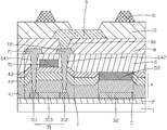
- FIG. 1 is a cross-sectional view showing a first embodiment of a TFT backplane structure of the present invention
- FIG. 2 is a cross-sectional view showing a second embodiment of a TFT backplane structure of the present invention
- FIG. 3 is a flow chart of a method of fabricating a TFT backplane of the present invention.
- a first embodiment of a TFT backplane structure of the present invention includes a substrate 1 , a buffer layer 2 covering the substrate 1 , and a polysilicon active layer 31 spaced apart from each other on the buffer layer 2 .
- Doped ions are implanted on both sides of the polysilicon active layer 31 to form a source contact region 311 and a drain contact region 312, respectively, and a channel region is formed between the source contact region 311 and the drain contact region 312. 313.
- the source 71 and the drain 72 pass through the interlayer insulating layer 6 and the gate insulating layer 4, respectively.
- the first via 641 and the second via 642 contact the source contact region 311 and the drain contact region 312.
- the pixel electrode 9 contacts the drain 72 via a third via 81 penetrating the planar layer 8.
- the polysilicon active layer 31, the gate electrode 51, the source electrode 71, and the drain electrode 72 constitute a TFT T, and the polysilicon electrode plate 32 and the metal electrode plate 52 constitute a storage capacitor C.
- the gate insulating layer 4 has a three-layer structure corresponding to the region where the TFT is located, and is sequentially composed of a dielectric layer 41 and a silicon nitride (SiNx) layer from bottom to top. 42.
- the silicon dioxide (SiO 2 ) layer 43; the gate insulating layer 4 has a two-layer structure corresponding to a region where the storage capacitor C is located, and is a dielectric layer 41 and at least a portion of the silicon nitride layer from bottom to top. 42.
- the dielectric layer 41 is a silicon dioxide layer.
- the advantage of this arrangement is that the silicon dioxide layer 43 located at the uppermost layer of the gate insulating layer 4 can effectively prevent the gate electrode 51 from injecting carriers into the silicon nitride layer 42 to protect the silicon nitride corresponding to the region where the TFT is located.
- the layer 42 is not damaged, and the reliability of the silicon dioxide layer 43 is superior to that of the silicon nitride layer 42, the influence of the carrier is small, the quality of the gate insulating layer 4 is ensured, and the silicon dioxide layer 43 is secured.
- the thickness of the gate insulating layer 4 is thinned corresponding to the region where the storage capacitor C is located, silicon dioxide
- the composition is reduced, the dielectric constant is increased, and the distance between the polysilicon electrode plate 32 and the metal electrode plate 52 of the storage capacitor C is reduced, thereby being able to reduce the storage capacitor performance (mainly the capacitance storage capacity).
- the area of the capacitor C increases the aperture ratio.
- the substrate 1 is preferably a glass substrate.
- the thickness of the buffer layer 2 is It may be a single layer of silicon nitride layer, a single layer of silicon oxide (SiOx) layer, or a superposition of a silicon nitride layer and a silicon oxide layer.
- the thickness of the polysilicon active layer 31 and the polysilicon electrode plate 32 are both the thickness of the polysilicon active layer 31 and the polysilicon electrode plate 32.
- the thickness of the dielectric layer 41 serving by the silicon dioxide layer is The thickness of the silicon nitride layer 42 is The thickness of the silicon dioxide layer 43 is
- the gate electrode 51 and the metal electrode plate 52 are both a molybdenum/aluminum/molybdenum (Mo/Al/Mo) laminated structure, or a molybdenum/aluminum (Mo/Al) laminated structure, and the thickness is
- the doping ions implanted on both sides of the polysilicon active layer 31 are phosphorus ions (P+) or boron ions (B+), and correspondingly, the TFT T is an N-type TFT or a P-type TFT.
- the thickness of the interlayer insulating layer 6 is It may be a single layer of silicon nitride layer, a single layer of silicon oxide layer, or a superposition of a silicon nitride layer and a silicon oxide layer.
- the source 71 and the drain 72 are both a Mo/Al/Mo laminated structure, or a Mo/Al laminated structure, and the thickness is
- the material of the pixel electrode 9 is Indium Tin Oxid (ITO).
- a second embodiment of the TFT backplane structure of the present invention is different from the first embodiment in that the gate insulating layer 4 has a three-layer structure corresponding to the region where the TFT T is located.
- the bottom layer is a dielectric layer 41, a silicon nitride layer 42, and a silicon dioxide layer 43.
- the region of the gate insulating layer 4 corresponding to the storage capacitor C is a single layer structure, and only the dielectric layer 41 is included.
- the dielectric layer 41 is an aluminum oxide (Al 3 O 2 ) layer, a titanium dioxide (TiO 2 ) layer, a zirconium dioxide (ZrO 2 ) layer, or cerium oxide.
- the high dielectric constant layer is used instead of the silicon dioxide layer to serve as the dielectric layer 41.
- the thickness of the region of the gate insulating layer 4 corresponding to the storage capacitor C can be further thinned. Only the dielectric layer 41 serving as the high dielectric constant layer is retained, so that the area of the capacitance C can be further reduced, and the aperture ratio can be improved.
- the present invention further provides a method for fabricating a TFT backplane, including the following steps:
- Step 1 Provide a cleaned and prebaked substrate 1.
- the substrate 1 is preferably a glass substrate.
- Step 2 Depositing a buffer layer 2 and an amorphous silicon layer on the substrate 1 in this order.
- the thickness of the buffer layer 2 is It may be a single layer of silicon nitride layer, a single layer of silicon oxide layer, or a superposition of a silicon nitride layer and a silicon oxide layer.
- the thickness of the amorphous silicon layer is
- Step 3 The amorphous silicon layer is crystallized into a polysilicon layer by an Excimer Laser Annealing (ELA) process or a Solid Phase Crystallization (SPC) process, and the polysilicon layer is patterned and defined.
- ELA Excimer Laser Annealing
- SPC Solid Phase Crystallization
- Step 4 sequentially depositing a dielectric layer 41, a silicon nitride layer 42, and a silicon dioxide layer 43 on the buffer layer 2, the polysilicon active layer 31, and the polysilicon electrode plate 32 from bottom to top to form a gate insulating layer. 4.
- the thickness of the dielectric layer 41 is The thickness of the silicon nitride layer 42 is The thickness of the silicon dioxide layer 43 is
- the dielectric layer 41 is a silicon dioxide layer.
- the dielectric layer 41 is a high dielectric constant layer such as an aluminum oxide layer, a titanium dioxide layer, a zirconium dioxide layer, or a hafnium oxide layer.
- Step 5 etching the gate insulating layer 4 corresponding to the region where the storage capacitor is to be formed by a photolithography process, as shown in FIG. 1, etching away all the silicon dioxide layer 43 and a portion of the silicon nitride layer 42 in the region.
- FIG. 2 all of the silicon dioxide layer 43 and all of the silicon nitride layer 42 in the region are etched away.
- the thickness of the gate insulating layer 4 corresponding to the region where the storage capacitor is to be formed is formed.
- the thinning was carried out.
- Step 6 Depositing and patterning a first metal layer on the gate insulating layer 4 to form a gate electrode 51 and a metal electrode plate 52.
- the gate electrode 51 is located above the polysilicon active layer 31.
- the electrode plate 52 is located above the polysilicon electrode plate 32.
- the polysilicon electrode plate 32 and the metal electrode plate 52 constitute a storage capacitor C.
- the first metal layer is a Mo/Al/Mo layered structure, or a Mo/Al layered structure, and the thickness is
- Step 7 implanting doping ions on both sides of the polysilicon active layer 31 by using the gate electrode 51 and the metal electrode plate 52 as a shielding layer, respectively forming a source contact region 311 and a drain contact region 312, and the source contacts A channel region 313 is formed between the region 311 and the drain contact region 312.
- the step 7 may select a phosphine (PH 3 ) gas source to implant P+ ions, or a diborane (B 2 H 6 ) gas source to implant B+ ions.
- a phosphine (PH 3 ) gas source to implant P+ ions
- a diborane (B 2 H 6 ) gas source to implant B+ ions.
- Step 8 Depositing and patterning the interlayer insulating layer 6 on the gate insulating layer 4, the gate electrode 51, and the metal electrode plate 52 to form portions of the source contact region 311 and the drain contact region 312, respectively.
- the thickness of the interlayer insulating layer 6 is It may be a single layer of silicon nitride layer, a single layer of silicon oxide layer, or a superposition of a silicon nitride layer and a silicon oxide layer.
- Step 9 Depositing and patterning a second metal layer on the interlayer insulating layer 6 to form a source 71 and a drain 72.
- the source 71 and the drain 72 pass through the first via 641 and the second via, respectively.
- the hole 642 contacts the source contact region 311 and the drain contact region 312.
- the polysilicon active layer 31, the gate 51, the source 71, and the drain 72 constitute a TFT T. If the above step 7 implants P+ ions, the TFT T is an N-type TFT; if the above step 7 implants B+ ions, the TFT T is a P-type TFT.
- the second metal layer is a Mo/Al/Mo laminated structure, or a Mo/Al laminated structure, and has a thickness of
- step 10 the flat layer 8, the pixel electrode 9, the pixel defining layer 10, and the photoresist spacer 11 are sequentially formed on the interlayer insulating layer 6, the source 71, and the drain 72 from bottom to top.
- the pixel electrode 9 contacts the drain 72 via a third via 81 penetrating the planar layer 8.
- the material of the pixel electrode 9 is ITO.
- the structure of the TFT backplane fabricated by the above method is as shown in FIG. 1 or FIG. 2, and the gate insulating layer 4 has a three-layer structure corresponding to the region where the TFT is located, and is sequentially composed of a dielectric layer 41 and nitrogen from bottom to top.
- the silicon layer 42 and the silicon dioxide layer 43 are located on the uppermost layer of the gate insulating layer 4, and the silicon dioxide layer 43 can effectively prevent the gate electrode 51 from injecting carriers into the silicon nitride layer 42 to protect the silicon nitride layer.
- the silicon dioxide layer 43 is superior to that of the silicon nitride layer 42, the influence of the carrier is small, the quality of the gate insulating layer 4 is ensured, and the silicon dioxide layer 43 is also It is possible to prevent the silicon nitride layer 42 from being over-etched when the gate electrode 51 is etched, so that the reliability of the TFT can be enhanced.
- the gate insulating layer 4 has a two-layer structure, which is a dielectric layer 41 serving as a silicon dioxide layer and at least a portion of the silicon nitride layer 42 from bottom to top; or
- the gate insulating layer 4 is a single-layer structure including only the dielectric layer 41 serving as a high dielectric constant layer such as an Al 3 O 2 layer, a TiO 2 layer, a ZrO 2 layer, or an HfO 2 layer, and the gate insulating layer 4
- the thickness is reduced, the silicon dioxide composition is reduced, the dielectric constant is increased, and the distance between the polysilicon electrode plate 32 and the metal electrode plate 52 of the storage capacitor C is reduced, thereby ensuring storage capacitor performance (mainly capacitance) Under the premise of storage capacity, the area of the capacitor C is reduced, and the aperture ratio is increased.
- the TFT backplane structure of the present invention has a three-layer structure in which the gate insulating layer corresponds to the region where the TFT is located, and is a dielectric layer, a silicon nitride layer, and a silicon dioxide layer from bottom to top.
- the gate insulating layer corresponds to the storage capacitor is a two-layer structure, and the bottom layer is a dielectric layer, at least partially a silicon nitride layer, or the gate insulating layer corresponds to
- the area where the storage capacitor is located is a single-layer structure, including only the dielectric layer, which can increase the dielectric constant and reduce the distance between the two electrode plates of the storage capacitor, thereby reducing the capacitance area under the premise of ensuring the performance of the storage capacitor.
- the gate insulating layer corresponding to the region where the storage capacitor is to be formed is etched by a photolithography process, and all of the silicon dioxide layer and a portion of the silicon nitride layer in the region are etched away, or etched. All the silicon dioxide layers and all the silicon nitride layers in the region are removed, so that the gate insulating layer in the TFT backplane prepared by the method corresponds to the region where the TFT is located, and the gate insulating layer corresponds to the gate insulating layer.
- the area where the storage capacitor is located is a two-layer structure or a single-layer structure, so that the TFT backplane has both strong reliability and can reduce the capacitance area and increase the aperture ratio under the premise of ensuring the performance of the storage capacitor.
Landscapes
- Thin Film Transistor (AREA)
- Chemical & Material Sciences (AREA)
- Chemical Kinetics & Catalysis (AREA)
- General Chemical & Material Sciences (AREA)
- Liquid Crystal (AREA)
Abstract
一种TFT背板结构及其制作方法。该TFT背板结构设置栅极绝缘层(4)对应于TFT(T)所在的区域为三层结构,自下至上依次为介电层(41)、氮化硅层(42)与二氧化硅层(43),能够增强TFT(T)的可靠性;设置栅极绝缘层(4)对应于存储电容(C)所在的区域为双层结构,自下至上依次为介电层(41)、与至少部分氮化硅层(42),或者所述栅极绝缘层(4)对应于存储电容(C)所在的区域为单层结构,仅包括介电层(41),能够增大介电常数,减小存储电容(C)两电极板之间的距离,从而能够在保证存储电容(C)性能的前提下,减少电容面积,提高开口率。
Description
本发明涉及显示技术领域,尤其涉及一种TFT背板结构及其制作方法。
在显示技术领域,液晶显示器(Liquid Crystal Display,LCD)与有机发光二极管显示器(Organic Light Emitting Diode,OLED)等平板显示技术已经逐步取代CRT显示器。其中,OLED具有自发光、驱动电压低、发光效率高、响应时间短、清晰度与对比度高、近180°视角、使用温度范围宽,可实现柔性显示与大面积全色显示等诸多优点,被业界公认为是最有发展潜力的显示装置。
OLED按照驱动类型可分为无源OLED(PMOLED)和有源OLED(AMOLED)。低温多晶硅(Low Temperature Poly-Silicon,LTPS)薄膜晶体管(Thin Film Transistor,TFT)在高分辨AMOLED技术中得到了业界的重视,有很大的应用价值和潜力。与非晶硅(a-Si)相比,LTPS TFT具有较高的载流子迁移率,器件反应速度快,稳定性好,可以满足高分辨率AMOLED显示器的要求。
现有技术中常见的适用于AMOLED的低温多晶硅TFT背板中的栅极绝缘层(Gate Insulation,GI)通常采用二氧化硅/氮化硅(SiO2/SiNx)的双层结构,其中SiO2层接触多晶硅有源层,SiNx层接触栅极(Gate)。SiNx层相比SiO2层,有较好的阻挡钠离子(Na+)、钾离子(K+)等可移动离子的能力,并且介电常数更大,相同的绝缘能力下可以比SiO2层做得更薄,且SiNx层氢(H)含量较多,可以对多晶硅中的悬空键起到钝化作用。但是SiNx层与多晶硅有源层的接触由于应力原因,界面性质不好,所以通常需要先沉积一层SiO2层,再加一层SiNx层构成栅极绝缘层。
SiNx层越厚,阻挡可移动离子以及钝化的效果越好,但随之而来的是TFT器件的可靠性下降,这是因为栅极不断地将载流子注入SiNx层,从而会破坏SiNx层,使得SiNx层的品质变差,导致TFT器件的可靠性降低,所以一般情况下,SiNx层都不会做的太厚;另外,在蚀刻制作栅极的过程中往往会对SiNx层造成过蚀刻。若为了保护SiNx层而单纯在SiNx层上叠加保护层则会使得存储电容区对应的栅极绝缘层的厚度同时增大,造成电容存储性能下降,只能以增大电容面积、牺牲开口率的方式来保证电容的
存储性能。
发明内容
本发明的目的在于提供一种TFT背板结构,既能够增强TFT的可靠性,又能够在保证存储电容性能的前提下,减少电容面积,提高开口率。
本发明的另一目的在于提供一种TFT背板的制作方法,通过该方法制作的TFT背板既具有较强的可靠性,又能够在保证存储电容性能的前提下,减少电容面积,提高开口率。
为实现上述目的,本发明首先提供一种TFT背板结构,包括基板、覆盖所述基板的缓冲层、设于所述缓冲层上相互间隔开的多晶硅有源层与多晶硅电极板、覆盖所述多晶硅有源层、多晶硅电极板、与缓冲层的栅极绝缘层、于所述多晶硅有源层上方设于栅极绝缘层上的栅极、于所述多晶硅电极板上方设于栅极绝缘层上的金属电极板、覆盖所述栅极、金属电极板、与栅极绝缘层的层间绝缘层、及设于所述层间绝缘层上的源极与漏极;
所述多晶硅有源层、栅极、源极、与漏极构成TFT,所述多晶硅电极板与金属电极板构成存储电容;
所述栅极绝缘层对应于TFT所在的区域为三层结构,自下至上依次为介电层、氮化硅层、与二氧化硅层;所述栅极绝缘层对应于存储电容所在的区域为双层结构,自下至上依次为介电层、与至少部分氮化硅层;或者所述栅极绝缘层对应于存储电容所在的区域为单层结构,仅包括介电层。
所述多晶硅有源层的两侧均植入掺杂离子,分别构成源极接触区与漏极接触区,所述源极接触区与漏极接触区之间构成沟道区;所述源极与漏极分别经由贯穿层间绝缘层和栅极绝缘层的第一过孔与第二过孔接触所述源极接触区与漏极接触区。
所述TFT背板结构还包括覆盖所述源极、漏极、与层间绝缘层的平坦层、设于所述平坦层上的像素电极、设于所述像素电极与平坦层上的像素定义层、及设于所述像素定义层上的光阻间隔物;
所述像素电极经由贯穿所述平坦层的第三过孔接触所述漏极。
所述介电层为二氧化硅层。
所述介电层为三氧化二铝层、二氧化钛层、二氧化锆层、或二氧化铪层。
本发明还提供一种TFT背板的制作方法,包括如下步骤:
步骤1、提供一经过清洗和预烘烤的基板;
步骤2、在所述基板上依次沉积形成缓冲层、与非晶硅层;
步骤3、通过准分子激光退火制程或固相晶化制程使非晶硅层结晶转变为多晶硅层,并对多晶硅层进行图案化处理,定义出多晶硅有源层、与多晶硅电极板;
步骤4、于所述缓冲层、多晶硅有源层、与多晶硅电极板上自下至上依次沉积介电层、氮化硅层、与二氧化硅层,形成栅极绝缘层;
步骤5、通过光刻制程对欲形成存储电容所在区域对应的栅极绝缘层进行蚀刻,蚀刻掉该区域内全部的二氧化硅层以及部分氮化硅层或者蚀刻掉该区域内全部的二氧化硅层以及全部的氮化硅层;
步骤6、于所述栅极绝缘层上沉积并图案化第一金属层,形成栅极、与金属电极板,所述栅极位于所述多晶硅有源层上方,所述金属电极板位于多晶硅电极板上方;
所述多晶硅电极板与金属电极板构成存储电容;
步骤7、以栅极、与金属电极板为遮蔽层对多晶硅有源层的两侧植入掺杂离子,分别形源极接触区与漏极接触区,所述源极接触区与漏极接触区之间构成沟道区;
步骤8、于所述栅极绝缘层、栅极、与金属电极板上沉积并图案化层间绝缘层,形成分别暴露出所述源极接触区与漏极接触区部分表面的第一过孔与第二过孔;
步骤9、于所述层间绝缘层上沉积并图案化第二金属层,形成源极与漏极,所述源极与漏极分别经由第一过孔与第二过孔接触所述源极接触区与漏极接触区;
所述多晶硅有源层、栅极、源极、与漏极构成TFT。
所述TFT背板的制作方法还包括步骤10、于所述层间绝缘层、源极、与漏极上由下至上依次制作平坦层、像素电极、像素定义层、及光阻间隔物;
所述像素电极经由贯穿所述平坦层的第三过孔接触所述漏极。
所述步骤4中沉积的介电层为二氧化硅层。
所述步骤4中沉积的介电层为三氧化二铝层、二氧化钛层、二氧化锆层、或二氧化铪层。
所述步骤7中植入的掺杂离子为磷离子、或硼离子。
本发明还提供一种TFT背板的制作方法,包括如下步骤:
步骤1、提供一经过清洗和预烘烤的基板;
步骤2、在所述基板上依次沉积形成缓冲层、与非晶硅层;
步骤3、通过准分子激光退火制程或固相晶化制程使非晶硅层结晶转变
为多晶硅层,并对多晶硅层进行图案化处理,定义出多晶硅有源层、与多晶硅电极板;
步骤4、于所述缓冲层、多晶硅有源层、与多晶硅电极板上自下至上依次沉积介电层、氮化硅层、与二氧化硅层,形成栅极绝缘层;
步骤5、通过光刻制程对欲形成存储电容所在区域对应的栅极绝缘层进行蚀刻,蚀刻掉该区域内全部的二氧化硅层以及部分氮化硅层,或者蚀刻掉该区域内全部的二氧化硅层以及全部的氮化硅层;
步骤6、于所述栅极绝缘层上沉积并图案化第一金属层,形成栅极、与金属电极板,所述栅极位于所述多晶硅有源层上方,所述金属电极板位于多晶硅电极板上方;
所述多晶硅电极板与金属电极板构成存储电容;
步骤7、以栅极、与金属电极板为遮蔽层对多晶硅有源层的两侧植入掺杂离子,分别形源极接触区与漏极接触区,所述源极接触区与漏极接触区之间构成沟道区;
步骤8、于所述栅极绝缘层、栅极、与金属电极板上沉积并图案化层间绝缘层,形成分别暴露出所述源极接触区与漏极接触区部分表面的第一过孔与第二过孔;
步骤9、于所述层间绝缘层上沉积并图案化第二金属层,形成源极与漏极,所述源极与漏极分别经由第一过孔与第二过孔接触所述源极接触区与漏极接触区;
所述多晶硅有源层、栅极、源极、与漏极构成TFT;
还包括步骤10、于所述层间绝缘层、源极、与漏极上由下至上依次制作平坦层、像素电极、像素定义层、及光阻间隔物;
所述像素电极经由贯穿所述平坦层的第三过孔接触所述漏极;
其中,所述步骤4中沉积的介电层为二氧化硅层;
其中,所述步骤7中植入的掺杂离子为磷离子、或硼离子。
本发明的有益效果:本发明提供的一种TFT背板结构,通过设置栅极绝缘层对应于TFT所在的区域为三层结构,自下至上依次为介电层、氮化硅层、与二氧化硅层,由所述二氧化硅层来阻止栅极向氮化硅层注入载流子,保护氮化硅层不受破坏,并且所述二氧化硅层还可以防止对氮化硅层造成过蚀刻,从而能够增强TFT的可靠性;设置栅极绝缘层对应于存储电容所在的区域为双层结构,自下至上依次为介电层、与至少部分氮化硅层,或者所述栅极绝缘层对应于存储电容所在的区域为单层结构,仅包括介电层,能够增大介电常数,减小存储电容两电极板之间的距离,从而能够在
保证存储电容性能的前提下,减少电容面积,提高开口率。本发明提供的一种TFT背板的制作方法,通过光刻制程对欲形成存储电容所在区域对应的栅极绝缘层进行蚀刻,蚀刻掉该区域内全部的二氧化硅层以及部分氮化硅层,或者蚀刻掉该区域内全部的二氧化硅层以及全部的氮化硅层,使得由该方法制作的TFT背板中栅极绝缘层对应于TFT所在的区域为三层结构,而栅极绝缘层对应于存储电容所在的区域为双层结构或单层结构,从而使得TFT背板既具有较强的可靠性,又能够在保证存储电容性能的前提下,减少电容面积,提高开口率。
为了能更进一步了解本发明的特征以及技术内容,请参阅以下有关本发明的详细说明与附图,然而附图仅提供参考与说明用,并非用来对本发明加以限制。
附图中,
图1为本发明的TFT背板结构第一实施例的剖面示意图;
图2为本发明的TFT背板结构第二实施例的剖面示意图;
图3为本发明的TFT背板的制作方法的流程图。
为更进一步阐述本发明所采取的技术手段及其效果,以下结合本发明的优选实施例及其附图进行详细描述。
本发明首先提供一种TFT背板结构。请参阅图1,为本发明的TFT背板结构的第一实施例,包括基板1、覆盖所述基板1的缓冲层2、设于所述缓冲层2上相互间隔开的多晶硅有源层31与多晶硅电极板32、覆盖所述多晶硅有源层31、多晶硅电极板32、与缓冲层2的栅极绝缘层4、于所述多晶硅有源层31上方设于栅极绝缘层4上的栅极51、于所述多晶硅电极板32上方设于栅极绝缘层4上的金属电极板52、覆盖所述栅极51、金属电极板52、与栅极绝缘层4的层间绝缘层6、及设于所述层间绝缘层6上的源极71与漏极72,还包括覆盖所述源极71、漏极72、与层间绝缘层6的平坦层8、设于所述平坦层8上的像素电极9、设于所述像素电极9与平坦层8上的像素定义层10、及设于所述像素定义层10上的光阻间隔物11。
所述多晶硅有源层31的两侧均植入掺杂离子,分别构成源极接触区311与漏极接触区312,所述源极接触区311与漏极接触区312之间构成沟道区313。所述源极71与漏极72分别经由贯穿层间绝缘层6和栅极绝缘层4的
第一过孔641与第二过孔642接触所述源极接触区311与漏极接触区312。所述像素电极9经由贯穿所述平坦层8的第三过孔81接触所述漏极72。
所述多晶硅有源层31、栅极51、源极71、与漏极72构成TFT T,所述多晶硅电极板32与金属电极板52构成存储电容C。
重点需要说明的是,在该第一实施例中,所述栅极绝缘层4对应于TFT所在的区域为三层结构,自下至上依次为由介电层41、氮化硅(SiNx)层42、与二氧化硅(Si02)层43;所述栅极绝缘层4对应于存储电容C所在的区域为双层结构,自下至上依次为介电层41、与至少部分氮化硅层42。进一步地,在该第一实施例中,所述介电层41为二氧化硅层。这样设置的益处在于:对应于TFT所在的区域,位于所述栅极绝缘层4最上层的二氧化硅层43能够有效阻止栅极51向氮化硅层42注入载流子,保护氮化硅层42不受破坏,而二氧化硅层43的可靠性优于氮化硅层42,受载流子的影响较小,栅极绝缘层4的品质得以保证,并且所述二氧化硅层43还可以防止在蚀刻栅极51时对氮化硅层42造成过蚀刻,从而能够增强TFT的可靠性;对应于存储电容C所在的区域,栅极绝缘层4的厚度得以减薄,二氧化硅成分减少,增大了介电常数,减小了存储电容C的多晶硅电极板32与金属电极板52之间的距离,从而能够在保证存储电容性能(主要是电容存储容量)的前提下,减少电容C的面积,提高开口率。
具体地,所述基板1优选为玻璃基板。
所述缓冲层2的厚度为 可为单层氮化硅层、单层氧化硅(SiOx)层、或氮化硅层与氧化硅层的叠加。
所述多晶硅有源层31与多晶硅电极板32的厚度均为
所述由二氧化硅层充当的介电层41的厚度为 氮化硅层42的厚度为
 二氧化硅层43的厚度为
所述栅极51与金属电极板52均为钼/铝/钼(Mo/Al/Mo)层叠结构,或钼/铝(Mo/Al)层叠结构,厚度均为
所述多晶硅有源层31的两侧均植入的掺杂离子为磷离子(P+)、或硼离子(B+),相应的,所述TFT T为N型TFT、或P型TFT。
所述层间绝缘层6的厚度为 可为单层氮化硅层、单层氧化硅层、或氮化硅层与氧化硅层的叠加。
所述源极71与漏极72均为Mo/Al/Mo层叠结构,或Mo/Al层叠结构,厚度均为
所述像素电极9的材料为氧化铟锡(Indium Tin Oxid,ITO)。
请参阅图2,为本发明的TFT背板结构的第二实施例,其与上述第一
实施例的区别在于:所述栅极绝缘层4对应于TFT T所在的区域为三层结构,自下至上依次为介电层41、氮化硅层42、与二氧化硅层43;所述栅极绝缘层4对应于存储电容C所在的区域为单层结构,仅包括介电层41。进一步地,在该第二实施例中,所述介电层41为三氧化二铝(Al3O2)层、二氧化钛(TiO2)层、二氧化锆(ZrO2)层、或二氧化铪(HfO2)层等高介电常数层。该实施例二采用高介电常数层来取代二氧化硅层充当介电层41,相比于实施例一能够进一步减薄所述栅极绝缘层4对应于存储电容C所在的区域的厚度,仅保留高介电常数层充当的介电层41,从而能够进一步减少电容C的面积,提高开口率。
请参阅图3,结合图1或图2,本发明还提供一种TFT背板的制作方法,包括如下步骤:
步骤1、提供一经过清洗和预烘烤的基板1。
所述基板1优选为玻璃基板。
步骤2、在所述基板1上依次沉积形成缓冲层2、与非晶硅层。
具体地,所述缓冲层2的厚度为 可为单层氮化硅层、单层氧化硅层、或氮化硅层与氧化硅层的叠加。
所述非晶硅层的厚度均为
步骤3、通过准分子激光退火(Excimer Laser Annealing,ELA)制程或固相晶化(Solid Phase Crystallization,SPC)制程使非晶硅层结晶转变为多晶硅层,并对多晶硅层进行图案化处理,定义出相互间隔开的多晶硅有源层31、与多晶硅电极板32。
步骤4、于所述缓冲层2、多晶硅有源层31、与多晶硅电极板32上自下至上依次沉积介电层41、氮化硅层42、与二氧化硅层43,形成栅极绝缘层4。
具体地,所述介电层41的厚度为 氮化硅层42的厚度为
 二氧化硅层43的厚度为
可选地,如图1所示,所述介电层41为二氧化硅层。
可选地,如图2所示,所述介电层41为三氧化二铝层、二氧化钛层、二氧化锆层、或二氧化铪层等高介电常数层。
步骤5、通过光刻制程对欲形成存储电容所在区域对应的栅极绝缘层4进行蚀刻,如图1所示,蚀刻掉该区域内全部的二氧化硅层43以及部分氮化硅层42,或者如图2所示,蚀刻掉该区域内全部的二氧化硅层43以及全部的氮化硅层42。
通过该步骤5对欲形成存储电容所在区域对应的栅极绝缘层4的厚度
进行了减薄。
步骤6、于所述栅极绝缘层4上沉积并图案化第一金属层,形成栅极51、与金属电极板52,所述栅极51位于所述多晶硅有源层31上方,所述金属电极板52位于多晶硅电极板32上方。
所述多晶硅电极板32与金属电极板52构成存储电容C。
具体地,所述第一金属层为Mo/Al/Mo层叠结构,或Mo/Al层叠结构,厚度为
步骤7、以栅极51、与金属电极板52为遮蔽层对多晶硅有源层31的两侧植入掺杂离子,分别形源极接触区311与漏极接触区312,所述源极接触区311与漏极接触区312之间构成沟道区313。
具体地,该步骤7可选择磷化氢(PH3)气源植入P+离子,或选择乙硼烷(B2H6)气源植入B+离子。
步骤8、于所述栅极绝缘层4、栅极51、与金属电极板52上沉积并图案化层间绝缘层6,形成分别暴露出所述源极接触区311与漏极接触区312部分表面的第一过孔641与第二过孔642。
具体地,所述层间绝缘层6的厚度为 可为单层氮化硅层、单层氧化硅层、或氮化硅层与氧化硅层的叠加。
步骤9、于所述层间绝缘层6上沉积并图案化第二金属层,形成源极71与漏极72,所述源极71与漏极72分别经由第一过孔641与第二过孔642接触所述源极接触区311与漏极接触区312。
所述多晶硅有源层31、栅极51、源极71、与漏极72构成TFT T。若上述步骤7植入的是P+离子,则所述TFT T为N型TFT;若上述步骤7植入的是B+离子,则所述TFT T为P型TFT。
具体地,所述第二金属层为Mo/Al/Mo层叠结构,或Mo/Al层叠结构,厚度为
以及步骤10、于所述层间绝缘层6、源极71、与漏极72上由下至上依次制作平坦层8、像素电极9、像素定义层10、及光阻间隔物11。
具体地,所述像素电极9经由贯穿所述平坦层8的第三过孔81接触所述漏极72。所述像素电极9的材料为ITO。
由上述方法制作的TFT背板的结构如图1或图2所示,对应于TFT所在的区域,所述栅极绝缘层4为三层结构,自下至上依次为由介电层41、氮化硅层42、与二氧化硅层43,位于所述栅极绝缘层4最上层的二氧化硅层43能够有效阻止栅极51向氮化硅层42注入载流子,保护氮化硅层42不受破坏,而二氧化硅层43的可靠性优于氮化硅层42,受载流子的影响较
小,栅极绝缘层4的品质得以保证,并且所述二氧化硅层43还可以防止在蚀刻栅极51时对氮化硅层42造成过蚀刻,从而能够增强TFT的可靠性。对应于存储电容C所在的区域,所述栅极绝缘层4为双层结构,自下至上依次为由二氧化硅层充当的介电层41、与至少部分氮化硅层42;或者所述栅极绝缘层4为单层结构,仅包括由Al3O2层、TiO2层、ZrO2层、或HfO2层等高介电常数层充当的介电层41,栅极绝缘层4的厚度得以减薄,二氧化硅成分减少,增大了介电常数,减小了存储电容C的多晶硅电极板32与金属电极板52之间的距离,从而能够在保证存储电容性能(主要是电容存储容量)的前提下,减少电容C的面积,提高开口率。
综上所述,本发明的TFT背板结构,通过设置栅极绝缘层对应于TFT所在的区域为三层结构,自下至上依次为介电层、氮化硅层、与二氧化硅层,由所述二氧化硅层来阻止栅极向氮化硅层注入载流子,保护氮化硅层不受破坏,并且所述二氧化硅层还可以防止对氮化硅层造成过蚀刻,从而能够增强TFT的可靠性;设置栅极绝缘层对应于存储电容所在的区域为双层结构,自下至上依次为介电层、与至少部分氮化硅层,或者所述栅极绝缘层对应于存储电容所在的区域为单层结构,仅包括介电层,能够增大介电常数,减小存储电容两电极板之间的距离,从而能够在保证存储电容性能的前提下,减少电容面积,提高开口率。本发明的TFT背板的制作方法,通过光刻制程对欲形成存储电容所在区域对应的栅极绝缘层进行蚀刻,蚀刻掉该区域内全部的二氧化硅层以及部分氮化硅层,或者蚀刻掉该区域内全部的二氧化硅层以及全部的氮化硅层,使得由该方法制作的TFT背板中栅极绝缘层对应于TFT所在的区域为三层结构,而栅极绝缘层对应于存储电容所在的区域为双层结构或单层结构,从而使得TFT背板既具有较强的可靠性,又能够在保证存储电容性能的前提下,减少电容面积,提高开口率。
以上所述,对于本领域的普通技术人员来说,可以根据本发明的技术方案和技术构思作出其他各种相应的改变和变形,而所有这些改变和变形都应属于本发明后附的权利要求的保护范围。
Claims (12)
- 一种TFT背板结构,包括基板、覆盖所述基板的缓冲层、设于所述缓冲层上相互间隔开的多晶硅有源层与多晶硅电极板、覆盖所述多晶硅有源层、多晶硅电极板、与缓冲层的栅极绝缘层、于所述多晶硅有源层上方设于栅极绝缘层上的栅极、于所述多晶硅电极板上方设于栅极绝缘层上的金属电极板、覆盖所述栅极、金属电极板、与栅极绝缘层的层间绝缘层、及设于所述层间绝缘层上的源极与漏极;所述多晶硅有源层、栅极、源极、与漏极构成TFT,所述多晶硅电极板与金属电极板构成存储电容;所述栅极绝缘层对应于TFT所在的区域为三层结构,自下至上依次为介电层、氮化硅层、与二氧化硅层;所述栅极绝缘层对应于存储电容所在的区域为双层结构,自下至上依次为介电层、与至少部分氮化硅层;或者所述栅极绝缘层对应于存储电容所在的区域为单层结构,仅包括介电层。
- 如权利要求1所述的TFT背板结构,其中,所述多晶硅有源层的两侧均植入掺杂离子,分别构成源极接触区与漏极接触区,所述源极接触区与漏极接触区之间构成沟道区;所述源极与漏极分别经由贯穿层间绝缘层和栅极绝缘层的第一过孔与第二过孔接触所述源极接触区与漏极接触区。
- 如权利要求1所述的TFT背板结构,还包括覆盖所述源极、漏极、与层间绝缘层的平坦层、设于所述平坦层上的像素电极、设于所述像素电极与平坦层上的像素定义层、及设于所述像素定义层上的光阻间隔物;所述像素电极经由贯穿所述平坦层的第三过孔接触所述漏极。
- 如权利要求2所述的TFT背板结构,还包括覆盖所述源极、漏极、与层间绝缘层的平坦层、设于所述平坦层上的像素电极、设于所述像素电极与平坦层上的像素定义层、及设于所述像素定义层上的光阻间隔物;所述像素电极经由贯穿所述平坦层的第三过孔接触所述漏极。
- 如权利要求1所述的TFT背板结构,其中,所述介电层为二氧化硅层。
- 如权利要求1所述的TFT背板结构,其中,所述介电层为三氧化二铝层、二氧化钛层、二氧化锆层、或二氧化铪层。
- 一种TFT背板的制作方法,包括如下步骤:步骤1、提供一经过清洗和预烘烤的基板;步骤2、在所述基板上依次沉积形成缓冲层、与非晶硅层;步骤3、通过准分子激光退火制程或固相晶化制程使非晶硅层结晶转变为多晶硅层,并对多晶硅层进行图案化处理,定义出多晶硅有源层、与多晶硅电极板;步骤4、于所述缓冲层、多晶硅有源层、与多晶硅电极板上自下至上依次沉积介电层、氮化硅层、与二氧化硅层,形成栅极绝缘层;步骤5、通过光刻制程对欲形成存储电容所在区域对应的栅极绝缘层进行蚀刻,蚀刻掉该区域内全部的二氧化硅层以及部分氮化硅层,或者蚀刻掉该区域内全部的二氧化硅层以及全部的氮化硅层;步骤6、于所述栅极绝缘层上沉积并图案化第一金属层,形成栅极、与金属电极板,所述栅极位于所述多晶硅有源层上方,所述金属电极板位于多晶硅电极板上方;所述多晶硅电极板与金属电极板构成存储电容;步骤7、以栅极、与金属电极板为遮蔽层对多晶硅有源层的两侧植入掺杂离子,分别形源极接触区与漏极接触区,所述源极接触区与漏极接触区之间构成沟道区;步骤8、于所述栅极绝缘层、栅极、与金属电极板上沉积并图案化层间绝缘层,形成分别暴露出所述源极接触区与漏极接触区部分表面的第一过孔与第二过孔;步骤9、于所述层间绝缘层上沉积并图案化第二金属层,形成源极与漏极,所述源极与漏极分别经由第一过孔与第二过孔接触所述源极接触区与漏极接触区;所述多晶硅有源层、栅极、源极、与漏极构成TFT。
- 如权利要求7所述的TFT背板的制作方法,还包括步骤10、于所述层间绝缘层、源极、与漏极上由下至上依次制作平坦层、像素电极、像素定义层、及光阻间隔物;所述像素电极经由贯穿所述平坦层的第三过孔接触所述漏极。
- 如权利要求7所述的TFT背板的制作方法,其中,所述步骤4中沉积的介电层为二氧化硅层。
- 如权利要求7所述的TFT背板的制作方法,其中,所述步骤4中沉积的介电层为三氧化二铝层、二氧化钛层、二氧化锆层、或二氧化铪层。
- 如权利要求7所述的TFT背板的制作方法,其中,所述步骤7中植入的掺杂离子为磷离子、或硼离子。
- 一种TFT背板的制作方法,包括如下步骤:步骤1、提供一经过清洗和预烘烤的基板;步骤2、在所述基板上依次沉积形成缓冲层、与非晶硅层;步骤3、通过准分子激光退火制程或固相晶化制程使非晶硅层结晶转变为多晶硅层,并对多晶硅层进行图案化处理,定义出多晶硅有源层、与多晶硅电极板;步骤4、于所述缓冲层、多晶硅有源层、与多晶硅电极板上自下至上依次沉积介电层、氮化硅层、与二氧化硅层,形成栅极绝缘层;步骤5、通过光刻制程对欲形成存储电容所在区域对应的栅极绝缘层进行蚀刻,蚀刻掉该区域内全部的二氧化硅层以及部分氮化硅层,或者蚀刻掉该区域内全部的二氧化硅层以及全部的氮化硅层;步骤6、于所述栅极绝缘层上沉积并图案化第一金属层,形成栅极、与金属电极板,所述栅极位于所述多晶硅有源层上方,所述金属电极板位于多晶硅电极板上方;所述多晶硅电极板与金属电极板构成存储电容;步骤7、以栅极、与金属电极板为遮蔽层对多晶硅有源层的两侧植入掺杂离子,分别形源极接触区与漏极接触区,所述源极接触区与漏极接触区之间构成沟道区;步骤8、于所述栅极绝缘层、栅极、与金属电极板上沉积并图案化层间绝缘层,形成分别暴露出所述源极接触区与漏极接触区部分表面的第一过孔与第二过孔;步骤9、于所述层间绝缘层上沉积并图案化第二金属层,形成源极与漏极,所述源极与漏极分别经由第一过孔与第二过孔接触所述源极接触区与漏极接触区;所述多晶硅有源层、栅极、源极、与漏极构成TFT;还包括步骤10、于所述层间绝缘层、源极、与漏极上由下至上依次制作平坦层、像素电极、像素定义层、及光阻间隔物;所述像素电极经由贯穿所述平坦层的第三过孔接触所述漏极;其中,所述步骤4中沉积的介电层为二氧化硅层;其中,所述步骤7中植入的掺杂离子为磷离子、或硼离子。
Priority Applications (1)
| Application Number | Priority Date | Filing Date | Title |
|---|---|---|---|
| US14/912,923 US9997634B2 (en) | 2015-12-03 | 2016-01-29 | TFT backplane and manufacturing method thereof |
Applications Claiming Priority (2)
| Application Number | Priority Date | Filing Date | Title |
|---|---|---|---|
| CN201510882240.3A CN105514116B (zh) | 2015-12-03 | 2015-12-03 | Tft背板结构及其制作方法 |
| CN201510882240.3 | 2015-12-03 |
Publications (1)
| Publication Number | Publication Date |
|---|---|
| WO2017092173A1 true WO2017092173A1 (zh) | 2017-06-08 |
Family
ID=55721968
Family Applications (1)
| Application Number | Title | Priority Date | Filing Date |
|---|---|---|---|
| PCT/CN2016/072873 Ceased WO2017092173A1 (zh) | 2015-12-03 | 2016-01-29 | Tft背板结构及其制作方法 |
Country Status (3)
| Country | Link |
|---|---|
| US (2) | US9997634B2 (zh) |
| CN (1) | CN105514116B (zh) |
| WO (1) | WO2017092173A1 (zh) |
Cited By (1)
| Publication number | Priority date | Publication date | Assignee | Title |
|---|---|---|---|---|
| CN109887956A (zh) * | 2019-01-25 | 2019-06-14 | 武汉华星光电半导体显示技术有限公司 | 有机发光二极管柔性阵列基板 |
Families Citing this family (34)
| Publication number | Priority date | Publication date | Assignee | Title |
|---|---|---|---|---|
| CN105932032A (zh) * | 2016-06-16 | 2016-09-07 | 深圳市华星光电技术有限公司 | 一种阵列基板及其制备方法 |
| KR102716398B1 (ko) * | 2016-06-17 | 2024-10-11 | 삼성디스플레이 주식회사 | 유기 발광 표시 장치 및 유기 발광 표시 장치의 제조 방법 |
| CN106654041B (zh) * | 2016-12-05 | 2018-10-26 | 武汉华星光电技术有限公司 | 柔性oled显示器及其制作方法 |
| CN106707638B (zh) * | 2016-12-20 | 2020-08-11 | 厦门天马微电子有限公司 | 阵列基板及其制作方法、显示面板 |
| CN107359258A (zh) * | 2017-06-01 | 2017-11-17 | 深圳市华星光电技术有限公司 | 显示基板及其制造方法、显示装置 |
| CN107134461A (zh) * | 2017-06-28 | 2017-09-05 | 深圳市华星光电技术有限公司 | 薄膜晶体管阵列基板及其制备方法、oled显示装置 |
| US10566401B2 (en) | 2017-06-28 | 2020-02-18 | Shenzhen China Star Optoelectronics Semiconductor Display Technology Co., Ltd. | Thin film transistor array substrate and preparing method therefor, and OLED display device |
| CN107342297A (zh) * | 2017-06-28 | 2017-11-10 | 深圳市华星光电半导体显示技术有限公司 | 薄膜晶体管阵列基板及其制备方法、显示装置 |
| TWI678829B (zh) * | 2017-09-05 | 2019-12-01 | 創王光電股份有限公司 | 發光元件及其製造方法 |
| CN108598089B (zh) * | 2018-04-27 | 2020-09-29 | 武汉华星光电技术有限公司 | Tft基板的制作方法及tft基板 |
| CN108538861B (zh) * | 2018-05-04 | 2021-03-16 | 武汉华星光电技术有限公司 | 阵列基板及其制造方法、显示面板 |
| CN110416257A (zh) * | 2018-07-13 | 2019-11-05 | 广东聚华印刷显示技术有限公司 | 显示面板背板结构、其制备方法及顶发射型显示面板 |
| CN109212854B (zh) * | 2018-08-29 | 2021-06-01 | 武汉华星光电技术有限公司 | 一种ltps阵列基板的制造方法 |
| US11195863B2 (en) * | 2018-09-21 | 2021-12-07 | Shenzhen China Star Optoelectronics Semiconductor Display Technology Co., Ltd. | Display panel having a storage capacitor, manufacturing method the same thereof and display module having the same |
| CN109037037B (zh) * | 2018-09-27 | 2023-09-01 | 武汉华星光电技术有限公司 | 低温多晶硅层、薄膜晶体管及其制作方法 |
| CN109637932B (zh) * | 2018-11-30 | 2020-11-10 | 武汉华星光电技术有限公司 | 薄膜晶体管及其制备方法 |
| CN110112212A (zh) * | 2019-04-25 | 2019-08-09 | 深圳市华星光电技术有限公司 | 薄膜晶体管和阵列基板 |
| CN110137225A (zh) * | 2019-05-05 | 2019-08-16 | 深圳市华星光电半导体显示技术有限公司 | Oled显示面板及其制备方法 |
| CN110164878B (zh) * | 2019-06-10 | 2022-05-03 | 惠科股份有限公司 | 阵列基板及其制备方法 |
| KR102612405B1 (ko) * | 2019-07-09 | 2023-12-12 | 엘지디스플레이 주식회사 | 전자장치 |
| CN110571226B (zh) * | 2019-09-05 | 2021-03-16 | 深圳市华星光电半导体显示技术有限公司 | 一种显示面板及其制备方法 |
| CN110600517B (zh) | 2019-09-16 | 2021-06-01 | 深圳市华星光电半导体显示技术有限公司 | 一种显示面板及其制备方法 |
| CN110707101A (zh) | 2019-10-16 | 2020-01-17 | 深圳市华星光电半导体显示技术有限公司 | 阵列基板及其制作方法、显示面板 |
| CN110993644A (zh) * | 2019-11-06 | 2020-04-10 | 深圳市华星光电半导体显示技术有限公司 | Oled显示面板及制备方法 |
| CN110911466B (zh) * | 2019-11-29 | 2022-08-19 | 京东方科技集团股份有限公司 | 一种基板及其制备方法、母板的制备方法、掩膜版和蒸镀装置 |
| CN111463244A (zh) * | 2020-04-09 | 2020-07-28 | 京东方科技集团股份有限公司 | 显示基板及其制作方法、显示装置 |
| CN111710727A (zh) * | 2020-06-12 | 2020-09-25 | 深圳市华星光电半导体显示技术有限公司 | 一种阵列基板及其制备方法以及显示面板 |
| CN111668242A (zh) * | 2020-07-02 | 2020-09-15 | 深圳市华星光电半导体显示技术有限公司 | Oled显示面板及其制备方法 |
| KR102780920B1 (ko) * | 2020-09-02 | 2025-03-12 | 양쯔 메모리 테크놀로지스 씨오., 엘티디. | 반도체 디바이스에서 온칩 커패시터 구조를 형성하기 위한 방법 |
| CN112086576B (zh) * | 2020-09-07 | 2022-09-09 | 武汉华星光电半导体显示技术有限公司 | 一种显示面板及制程方法 |
| CN113517225A (zh) * | 2021-03-30 | 2021-10-19 | 中山大学 | 基于全n型tft中心频率可调的带通放大电路制作方法 |
| CN113284910B (zh) * | 2021-04-29 | 2023-09-19 | 合肥鑫晟光电科技有限公司 | 显示背板、制作方法以及显示装置 |
| CN114220865A (zh) * | 2021-12-13 | 2022-03-22 | 深圳市华星光电半导体显示技术有限公司 | 薄膜晶体管及其制作方法、显示面板 |
| CN114823718B (zh) * | 2022-03-22 | 2026-01-06 | 福建华佳彩有限公司 | 一种ltpo背板结构及制作方法 |
Citations (3)
| Publication number | Priority date | Publication date | Assignee | Title |
|---|---|---|---|---|
| US20080128719A1 (en) * | 2006-12-01 | 2008-06-05 | Au Optronics Corporation | LCD Pixel Array Structure and Fabrication Method Thereof |
| CN103296034A (zh) * | 2013-05-28 | 2013-09-11 | 京东方科技集团股份有限公司 | 一种阵列基板、制备方法以及显示装置 |
| CN104538403A (zh) * | 2014-12-30 | 2015-04-22 | 厦门天马微电子有限公司 | 阵列基板单元结构、阵列基板、显示装置以及制作方法 |
Family Cites Families (4)
| Publication number | Priority date | Publication date | Assignee | Title |
|---|---|---|---|---|
| KR20060125066A (ko) * | 2005-06-01 | 2006-12-06 | 삼성전자주식회사 | 개구율이 향상된 어레이 기판 및 이의 제조방법 |
| US7381596B2 (en) * | 2005-09-26 | 2008-06-03 | Chunghwa Picture Tubes, Ltd. | Method of manufacturing an AMOLED |
| JP2012146805A (ja) * | 2011-01-12 | 2012-08-02 | Sony Corp | 放射線撮像装置、放射線撮像表示システムおよびトランジスタ |
| CN104022076B (zh) * | 2014-05-27 | 2017-01-25 | 京东方科技集团股份有限公司 | 阵列基板及其制作方法、显示装置 |
-
2015
- 2015-12-03 CN CN201510882240.3A patent/CN105514116B/zh not_active Expired - Fee Related
-
2016
- 2016-01-29 US US14/912,923 patent/US9997634B2/en active Active
- 2016-01-29 WO PCT/CN2016/072873 patent/WO2017092173A1/zh not_active Ceased
-
2018
- 2018-05-02 US US15/968,763 patent/US10269973B2/en not_active Expired - Fee Related
Patent Citations (3)
| Publication number | Priority date | Publication date | Assignee | Title |
|---|---|---|---|---|
| US20080128719A1 (en) * | 2006-12-01 | 2008-06-05 | Au Optronics Corporation | LCD Pixel Array Structure and Fabrication Method Thereof |
| CN103296034A (zh) * | 2013-05-28 | 2013-09-11 | 京东方科技集团股份有限公司 | 一种阵列基板、制备方法以及显示装置 |
| CN104538403A (zh) * | 2014-12-30 | 2015-04-22 | 厦门天马微电子有限公司 | 阵列基板单元结构、阵列基板、显示装置以及制作方法 |
Cited By (1)
| Publication number | Priority date | Publication date | Assignee | Title |
|---|---|---|---|---|
| CN109887956A (zh) * | 2019-01-25 | 2019-06-14 | 武汉华星光电半导体显示技术有限公司 | 有机发光二极管柔性阵列基板 |
Also Published As
| Publication number | Publication date |
|---|---|
| US20180248032A1 (en) | 2018-08-30 |
| US10269973B2 (en) | 2019-04-23 |
| CN105514116B (zh) | 2018-08-14 |
| US9997634B2 (en) | 2018-06-12 |
| CN105514116A (zh) | 2016-04-20 |
| US20180033883A1 (en) | 2018-02-01 |
Similar Documents
| Publication | Publication Date | Title |
|---|---|---|
| CN105514116B (zh) | Tft背板结构及其制作方法 | |
| US11790867B2 (en) | Active matrix substrate, liquid crystal display device, and organic EL display device | |
| US9768310B2 (en) | Thin film transistor, organic light-emitting diode display including the same, and manufacturing method thereof | |
| KR101233348B1 (ko) | 표시 장치 및 그 제조 방법 | |
| US9748280B2 (en) | Thin film transistor and method of fabricating the same, array substrate and method of fabricating the same, and display device | |
| US10937813B2 (en) | Active matrix substrate, liquid crystal display device, organic electroluminescent display device and method for producing active matrix substrate | |
| CN103730508B (zh) | 显示面板的垂直式薄膜晶体管结构及其制作方法 | |
| US10658446B2 (en) | Method for manufacturing OLED backplane comprising active layer formed of first, second, and third oxide semiconductor layers | |
| CN104465702B (zh) | Amoled背板的制作方法 | |
| US20160027887A1 (en) | Array substrate and fabrication method thereof, and display device | |
| CN104637438A (zh) | 柔性显示器及其制造方法 | |
| US9680122B1 (en) | Organic light emitting display device and method of manufacturing the same | |
| WO2016026246A1 (zh) | 薄膜晶体管及其制备方法、阵列基板及其制备方法和显示装置 | |
| WO2018188146A1 (zh) | 一种阵列基板、显示装置及其制作方法 | |
| US20150372021A1 (en) | Display device, array substrate and method for manufacturing the same | |
| CN104966718B (zh) | Amoled背板的制作方法及其结构 | |
| KR20140125186A (ko) | 박막 트랜지스터의 제조 방법, 이를 포함하는 유기 발광 표시 장치의 제조 방법 및 이를 통해 제조된 박막 트랜지스터와 유기 발광 표시 장치 | |
| US11895870B2 (en) | Display panel and display device | |
| KR20140131774A (ko) | 커패시터의 제조 방법, 이를 포함하는 유기 발광 표시 장치의 제조 방법 및 이를 통해 제조된 유기 발광 표시 장치 | |
| CN103681659A (zh) | 一种阵列基板、制备方法以及显示装置 | |
| CN107425044A (zh) | 一种柔性显示面板、其制作方法及显示装置 | |
| US20210376160A1 (en) | Thin film transistor, manufacturing method thereof, and display panel | |
| US9812541B2 (en) | Array substrate, method for fabricating the same and display device | |
| CN104040724B (zh) | 半导体装置、显示装置和半导体装置的制造方法 | |
| CN106992189A (zh) | 氧化物半导体tft基板结构及氧化物半导体tft基板的制作方法 |
Legal Events
| Date | Code | Title | Description |
|---|---|---|---|
| WWE | Wipo information: entry into national phase |
Ref document number: 14912923 Country of ref document: US |
|
| 121 | Ep: the epo has been informed by wipo that ep was designated in this application |
Ref document number: 16869487 Country of ref document: EP Kind code of ref document: A1 |
|
| NENP | Non-entry into the national phase |
Ref country code: DE |
|
| 122 | Ep: pct application non-entry in european phase |
Ref document number: 16869487 Country of ref document: EP Kind code of ref document: A1 |