WO2017081831A1 - 光センサ - Google Patents
光センサ Download PDFInfo
- Publication number
- WO2017081831A1 WO2017081831A1 PCT/JP2016/003348 JP2016003348W WO2017081831A1 WO 2017081831 A1 WO2017081831 A1 WO 2017081831A1 JP 2016003348 W JP2016003348 W JP 2016003348W WO 2017081831 A1 WO2017081831 A1 WO 2017081831A1
- Authority
- WO
- WIPO (PCT)
- Prior art keywords
- electrode
- photoelectric conversion
- layer
- conversion layer
- voltage
- Prior art date
Links
- 238000006243 chemical reaction Methods 0.000 claims abstract description 371
- 230000000903 blocking effect Effects 0.000 claims abstract description 163
- 238000001514 detection method Methods 0.000 claims abstract description 69
- 230000008859 change Effects 0.000 claims abstract description 58
- 230000005684 electric field Effects 0.000 claims abstract description 25
- 239000004065 semiconductor Substances 0.000 claims description 106
- 230000003287 optical effect Effects 0.000 claims description 81
- 238000004770 highest occupied molecular orbital Methods 0.000 claims description 20
- 238000004768 lowest unoccupied molecular orbital Methods 0.000 claims description 19
- 239000003990 capacitor Substances 0.000 claims description 18
- 239000010410 layer Substances 0.000 description 602
- 239000000463 material Substances 0.000 description 74
- 238000005036 potential barrier Methods 0.000 description 28
- 238000010586 diagram Methods 0.000 description 27
- 229910052718 tin Inorganic materials 0.000 description 27
- ATJFFYVFTNAWJD-UHFFFAOYSA-N Tin Chemical compound [Sn] ATJFFYVFTNAWJD-UHFFFAOYSA-N 0.000 description 26
- 239000010408 film Substances 0.000 description 26
- 150000001875 compounds Chemical class 0.000 description 22
- LKKPNUDVOYAOBB-UHFFFAOYSA-N naphthalocyanine Chemical compound N1C(N=C2C3=CC4=CC=CC=C4C=C3C(N=C3C4=CC5=CC=CC=C5C=C4C(=N4)N3)=N2)=C(C=C2C(C=CC=C2)=C2)C2=C1N=C1C2=CC3=CC=CC=C3C=C2C4=N1 LKKPNUDVOYAOBB-UHFFFAOYSA-N 0.000 description 22
- 150000002894 organic compounds Chemical class 0.000 description 21
- 239000000758 substrate Substances 0.000 description 20
- -1 carbamoyloxy group Chemical group 0.000 description 19
- 230000004888 barrier function Effects 0.000 description 16
- 239000010409 thin film Substances 0.000 description 15
- RBTKNAXYKSUFRK-UHFFFAOYSA-N heliogen blue Chemical compound [Cu].[N-]1C2=C(C=CC=C3)C3=C1N=C([N-]1)C3=CC=CC=C3C1=NC([N-]1)=C(C=CC=C3)C3=C1N=C([N-]1)C3=CC=CC=C3C1=N2 RBTKNAXYKSUFRK-UHFFFAOYSA-N 0.000 description 11
- 238000010521 absorption reaction Methods 0.000 description 10
- 238000003384 imaging method Methods 0.000 description 10
- 238000002347 injection Methods 0.000 description 10
- 239000007924 injection Substances 0.000 description 10
- 238000005259 measurement Methods 0.000 description 10
- VYPSYNLAJGMNEJ-UHFFFAOYSA-N Silicium dioxide Chemical compound O=[Si]=O VYPSYNLAJGMNEJ-UHFFFAOYSA-N 0.000 description 8
- 239000012535 impurity Substances 0.000 description 8
- 230000000717 retained effect Effects 0.000 description 8
- 229910052814 silicon oxide Inorganic materials 0.000 description 8
- XMWRBQBLMFGWIX-UHFFFAOYSA-N C60 fullerene Chemical class C12=C3C(C4=C56)=C7C8=C5C5=C9C%10=C6C6=C4C1=C1C4=C6C6=C%10C%10=C9C9=C%11C5=C8C5=C8C7=C3C3=C7C2=C1C1=C2C4=C6C4=C%10C6=C9C9=C%11C5=C5C8=C3C3=C7C1=C1C2=C4C6=C2C9=C5C3=C12 XMWRBQBLMFGWIX-UHFFFAOYSA-N 0.000 description 6
- RAXXELZNTBOGNW-UHFFFAOYSA-N imidazole Natural products C1=CNC=N1 RAXXELZNTBOGNW-UHFFFAOYSA-N 0.000 description 6
- 125000002080 perylenyl group Chemical class C1(=CC=C2C=CC=C3C4=CC=CC5=CC=CC(C1=C23)=C45)* 0.000 description 6
- 229920000301 poly(3-hexylthiophene-2,5-diyl) polymer Polymers 0.000 description 6
- 125000001424 substituent group Chemical group 0.000 description 6
- 229910018072 Al 2 O 3 Inorganic materials 0.000 description 5
- XUIMIQQOPSSXEZ-UHFFFAOYSA-N Silicon Chemical compound [Si] XUIMIQQOPSSXEZ-UHFFFAOYSA-N 0.000 description 5
- GVEPBJHOBDJJJI-UHFFFAOYSA-N fluoranthene Chemical class C1=CC(C2=CC=CC=C22)=C3C2=CC=CC3=C1 GVEPBJHOBDJJJI-UHFFFAOYSA-N 0.000 description 5
- 125000000623 heterocyclic group Chemical group 0.000 description 5
- 229910052710 silicon Inorganic materials 0.000 description 5
- 239000010703 silicon Substances 0.000 description 5
- OKTJSMMVPCPJKN-UHFFFAOYSA-N Carbon Chemical compound [C] OKTJSMMVPCPJKN-UHFFFAOYSA-N 0.000 description 4
- 239000010949 copper Substances 0.000 description 4
- 125000004431 deuterium atom Chemical group 0.000 description 4
- 239000011521 glass Substances 0.000 description 4
- 125000004435 hydrogen atom Chemical group [H]* 0.000 description 4
- 229910052751 metal Inorganic materials 0.000 description 4
- 239000002184 metal Substances 0.000 description 4
- 239000011368 organic material Substances 0.000 description 4
- CSHWQDPOILHKBI-UHFFFAOYSA-N peryrene Natural products C1=CC(C2=CC=CC=3C2=C2C=CC=3)=C3C2=CC=CC3=C1 CSHWQDPOILHKBI-UHFFFAOYSA-N 0.000 description 4
- 230000010287 polarization Effects 0.000 description 4
- 238000000862 absorption spectrum Methods 0.000 description 3
- 229910052782 aluminium Inorganic materials 0.000 description 3
- 238000000231 atomic layer deposition Methods 0.000 description 3
- 230000009286 beneficial effect Effects 0.000 description 3
- 230000008901 benefit Effects 0.000 description 3
- 230000000052 comparative effect Effects 0.000 description 3
- 239000000470 constituent Substances 0.000 description 3
- 229910003472 fullerene Inorganic materials 0.000 description 3
- 229910010272 inorganic material Inorganic materials 0.000 description 3
- 238000000034 method Methods 0.000 description 3
- 150000002790 naphthalenes Chemical class 0.000 description 3
- IEQIEDJGQAUEQZ-UHFFFAOYSA-N phthalocyanine Chemical class N1C(N=C2C3=CC=CC=C3C(N=C3C4=CC=CC=C4C(=N4)N3)=N2)=C(C=CC=C2)C2=C1N=C1C2=CC=CC=C2C4=N1 IEQIEDJGQAUEQZ-UHFFFAOYSA-N 0.000 description 3
- 150000003219 pyrazolines Chemical class 0.000 description 3
- XSCHRSMBECNVNS-UHFFFAOYSA-N quinoxaline Chemical compound N1=CC=NC2=CC=CC=C21 XSCHRSMBECNVNS-UHFFFAOYSA-N 0.000 description 3
- 229910052719 titanium Inorganic materials 0.000 description 3
- 239000010936 titanium Substances 0.000 description 3
- YBYIRNPNPLQARY-UHFFFAOYSA-N 1H-indene Chemical compound C1=CC=C2CC=CC2=C1 YBYIRNPNPLQARY-UHFFFAOYSA-N 0.000 description 2
- STTGYIUESPWXOW-UHFFFAOYSA-N 2,9-dimethyl-4,7-diphenyl-1,10-phenanthroline Chemical compound C=12C=CC3=C(C=4C=CC=CC=4)C=C(C)N=C3C2=NC(C)=CC=1C1=CC=CC=C1 STTGYIUESPWXOW-UHFFFAOYSA-N 0.000 description 2
- UJOBWOGCFQCDNV-UHFFFAOYSA-N 9H-carbazole Chemical compound C1=CC=C2C3=CC=CC=C3NC2=C1 UJOBWOGCFQCDNV-UHFFFAOYSA-N 0.000 description 2
- KAKZBPTYRLMSJV-UHFFFAOYSA-N Butadiene Chemical compound C=CC=C KAKZBPTYRLMSJV-UHFFFAOYSA-N 0.000 description 2
- SIKJAQJRHWYJAI-UHFFFAOYSA-N Indole Chemical compound C1=CC=C2NC=CC2=C1 SIKJAQJRHWYJAI-UHFFFAOYSA-N 0.000 description 2
- ZCQWOFVYLHDMMC-UHFFFAOYSA-N Oxazole Chemical compound C1=COC=N1 ZCQWOFVYLHDMMC-UHFFFAOYSA-N 0.000 description 2
- PCNDJXKNXGMECE-UHFFFAOYSA-N Phenazine Natural products C1=CC=CC2=NC3=CC=CC=C3N=C21 PCNDJXKNXGMECE-UHFFFAOYSA-N 0.000 description 2
- 239000004642 Polyimide Substances 0.000 description 2
- KYQCOXFCLRTKLS-UHFFFAOYSA-N Pyrazine Chemical compound C1=CN=CC=N1 KYQCOXFCLRTKLS-UHFFFAOYSA-N 0.000 description 2
- JUJWROOIHBZHMG-UHFFFAOYSA-N Pyridine Chemical compound C1=CC=NC=C1 JUJWROOIHBZHMG-UHFFFAOYSA-N 0.000 description 2
- KAESVJOAVNADME-UHFFFAOYSA-N Pyrrole Chemical compound C=1C=CNC=1 KAESVJOAVNADME-UHFFFAOYSA-N 0.000 description 2
- SMWDFEZZVXVKRB-UHFFFAOYSA-N Quinoline Chemical compound N1=CC=CC2=CC=CC=C21 SMWDFEZZVXVKRB-UHFFFAOYSA-N 0.000 description 2
- 229910004298 SiO 2 Inorganic materials 0.000 description 2
- 229910004166 TaN Inorganic materials 0.000 description 2
- YTPLMLYBLZKORZ-UHFFFAOYSA-N Thiophene Chemical compound C=1C=CSC=1 YTPLMLYBLZKORZ-UHFFFAOYSA-N 0.000 description 2
- XLOMVQKBTHCTTD-UHFFFAOYSA-N Zinc monoxide Chemical compound [Zn]=O XLOMVQKBTHCTTD-UHFFFAOYSA-N 0.000 description 2
- DZBUGLKDJFMEHC-UHFFFAOYSA-N acridine Chemical compound C1=CC=CC2=CC3=CC=CC=C3N=C21 DZBUGLKDJFMEHC-UHFFFAOYSA-N 0.000 description 2
- 229910021417 amorphous silicon Inorganic materials 0.000 description 2
- 150000001454 anthracenes Chemical class 0.000 description 2
- 150000001601 aromatic carbocyclic compounds Chemical class 0.000 description 2
- IOJUPLGTWVMSFF-UHFFFAOYSA-N benzothiazole Chemical compound C1=CC=C2SC=NC2=C1 IOJUPLGTWVMSFF-UHFFFAOYSA-N 0.000 description 2
- 239000002041 carbon nanotube Substances 0.000 description 2
- 229910021393 carbon nanotube Inorganic materials 0.000 description 2
- 150000004696 coordination complex Chemical class 0.000 description 2
- 229910052802 copper Inorganic materials 0.000 description 2
- ZSWFCLXCOIISFI-UHFFFAOYSA-N cyclopentadiene Chemical compound C1C=CC=C1 ZSWFCLXCOIISFI-UHFFFAOYSA-N 0.000 description 2
- 230000003247 decreasing effect Effects 0.000 description 2
- 230000000694 effects Effects 0.000 description 2
- 150000002484 inorganic compounds Chemical class 0.000 description 2
- AWJUIBRHMBBTKR-UHFFFAOYSA-N isoquinoline Chemical compound C1=NC=CC2=CC=CC=C21 AWJUIBRHMBBTKR-UHFFFAOYSA-N 0.000 description 2
- 239000003446 ligand Substances 0.000 description 2
- 150000004767 nitrides Chemical class 0.000 description 2
- 150000004866 oxadiazoles Chemical class 0.000 description 2
- 150000002987 phenanthrenes Chemical class 0.000 description 2
- 229910052697 platinum Inorganic materials 0.000 description 2
- 229920003229 poly(methyl methacrylate) Polymers 0.000 description 2
- 229920000412 polyarylene Chemical class 0.000 description 2
- 229920001721 polyimide Polymers 0.000 description 2
- 239000004926 polymethyl methacrylate Substances 0.000 description 2
- BBEAQIROQSPTKN-UHFFFAOYSA-N pyrene Chemical compound C1=CC=C2C=CC3=CC=CC4=CC=C1C2=C43 BBEAQIROQSPTKN-UHFFFAOYSA-N 0.000 description 2
- 150000003220 pyrenes Chemical class 0.000 description 2
- 239000000523 sample Substances 0.000 description 2
- 230000035945 sensitivity Effects 0.000 description 2
- 239000002109 single walled nanotube Substances 0.000 description 2
- 238000004544 sputter deposition Methods 0.000 description 2
- OFIYHXOOOISSDN-UHFFFAOYSA-N tellanylidenegallium Chemical compound [Te]=[Ga] OFIYHXOOOISSDN-UHFFFAOYSA-N 0.000 description 2
- 150000003518 tetracenes Chemical class 0.000 description 2
- 238000002834 transmittance Methods 0.000 description 2
- QGKMIGUHVLGJBR-UHFFFAOYSA-M (4z)-1-(3-methylbutyl)-4-[[1-(3-methylbutyl)quinolin-1-ium-4-yl]methylidene]quinoline;iodide Chemical class [I-].C12=CC=CC=C2N(CCC(C)C)C=CC1=CC1=CC=[N+](CCC(C)C)C2=CC=CC=C12 QGKMIGUHVLGJBR-UHFFFAOYSA-M 0.000 description 1
- UWRZIZXBOLBCON-VOTSOKGWSA-N (e)-2-phenylethenamine Chemical class N\C=C\C1=CC=CC=C1 UWRZIZXBOLBCON-VOTSOKGWSA-N 0.000 description 1
- POILWHVDKZOXJZ-ARJAWSKDSA-M (z)-4-oxopent-2-en-2-olate Chemical compound C\C([O-])=C\C(C)=O POILWHVDKZOXJZ-ARJAWSKDSA-M 0.000 description 1
- JYEUMXHLPRZUAT-UHFFFAOYSA-N 1,2,3-triazine Chemical compound C1=CN=NN=C1 JYEUMXHLPRZUAT-UHFFFAOYSA-N 0.000 description 1
- BCMCBBGGLRIHSE-UHFFFAOYSA-N 1,3-benzoxazole Chemical compound C1=CC=C2OC=NC2=C1 BCMCBBGGLRIHSE-UHFFFAOYSA-N 0.000 description 1
- VERMWGQSKPXSPZ-BUHFOSPRSA-N 1-[(e)-2-phenylethenyl]anthracene Chemical class C=1C=CC2=CC3=CC=CC=C3C=C2C=1\C=C\C1=CC=CC=C1 VERMWGQSKPXSPZ-BUHFOSPRSA-N 0.000 description 1
- HYZJCKYKOHLVJF-UHFFFAOYSA-N 1H-benzimidazole Chemical compound C1=CC=C2NC=NC2=C1 HYZJCKYKOHLVJF-UHFFFAOYSA-N 0.000 description 1
- BAXOFTOLAUCFNW-UHFFFAOYSA-N 1H-indazole Chemical compound C1=CC=C2C=NNC2=C1 BAXOFTOLAUCFNW-UHFFFAOYSA-N 0.000 description 1
- VEPOHXYIFQMVHW-XOZOLZJESA-N 2,3-dihydroxybutanedioic acid (2S,3S)-3,4-dimethyl-2-phenylmorpholine Chemical compound OC(C(O)C(O)=O)C(O)=O.C[C@H]1[C@@H](OCCN1C)c1ccccc1 VEPOHXYIFQMVHW-XOZOLZJESA-N 0.000 description 1
- MVWPVABZQQJTPL-UHFFFAOYSA-N 2,3-diphenylcyclohexa-2,5-diene-1,4-dione Chemical class O=C1C=CC(=O)C(C=2C=CC=CC=2)=C1C1=CC=CC=C1 MVWPVABZQQJTPL-UHFFFAOYSA-N 0.000 description 1
- FQJQNLKWTRGIEB-UHFFFAOYSA-N 2-(4-tert-butylphenyl)-5-[3-[5-(4-tert-butylphenyl)-1,3,4-oxadiazol-2-yl]phenyl]-1,3,4-oxadiazole Chemical compound C1=CC(C(C)(C)C)=CC=C1C1=NN=C(C=2C=C(C=CC=2)C=2OC(=NN=2)C=2C=CC(=CC=2)C(C)(C)C)O1 FQJQNLKWTRGIEB-UHFFFAOYSA-N 0.000 description 1
- BSKHPKMHTQYZBB-UHFFFAOYSA-N 2-methylpyridine Chemical compound CC1=CC=CC=N1 BSKHPKMHTQYZBB-UHFFFAOYSA-N 0.000 description 1
- HONWGFNQCPRRFM-UHFFFAOYSA-N 2-n-(3-methylphenyl)-1-n,1-n,2-n-triphenylbenzene-1,2-diamine Chemical compound CC1=CC=CC(N(C=2C=CC=CC=2)C=2C(=CC=CC=2)N(C=2C=CC=CC=2)C=2C=CC=CC=2)=C1 HONWGFNQCPRRFM-UHFFFAOYSA-N 0.000 description 1
- CAAMSDWKXXPUJR-UHFFFAOYSA-N 3,5-dihydro-4H-imidazol-4-one Chemical compound O=C1CNC=N1 CAAMSDWKXXPUJR-UHFFFAOYSA-N 0.000 description 1
- ONKCIMOQGCARHN-UHFFFAOYSA-N 3-methyl-n-[4-[4-(3-methylanilino)phenyl]phenyl]aniline Chemical compound CC1=CC=CC(NC=2C=CC(=CC=2)C=2C=CC(NC=3C=C(C)C=CC=3)=CC=2)=C1 ONKCIMOQGCARHN-UHFFFAOYSA-N 0.000 description 1
- DHDHJYNTEFLIHY-UHFFFAOYSA-N 4,7-diphenyl-1,10-phenanthroline Chemical compound C1=CC=CC=C1C1=CC=NC2=C1C=CC1=C(C=3C=CC=CC=3)C=CN=C21 DHDHJYNTEFLIHY-UHFFFAOYSA-N 0.000 description 1
- 150000000660 7-membered heterocyclic compounds Chemical class 0.000 description 1
- WRYCSMQKUKOKBP-UHFFFAOYSA-N Imidazolidine Chemical compound C1CNCN1 WRYCSMQKUKOKBP-UHFFFAOYSA-N 0.000 description 1
- UUIQMZJEGPQKFD-UHFFFAOYSA-N Methyl butyrate Chemical compound CCCC(=O)OC UUIQMZJEGPQKFD-UHFFFAOYSA-N 0.000 description 1
- 239000004793 Polystyrene Substances 0.000 description 1
- WTKZEGDFNFYCGP-UHFFFAOYSA-N Pyrazole Chemical compound C=1C=NNC=1 WTKZEGDFNFYCGP-UHFFFAOYSA-N 0.000 description 1
- CZPWVGJYEJSRLH-UHFFFAOYSA-N Pyrimidine Chemical compound C1=CN=CN=C1 CZPWVGJYEJSRLH-UHFFFAOYSA-N 0.000 description 1
- 229910006404 SnO 2 Inorganic materials 0.000 description 1
- FZWLAAWBMGSTSO-UHFFFAOYSA-N Thiazole Chemical compound C1=CSC=N1 FZWLAAWBMGSTSO-UHFFFAOYSA-N 0.000 description 1
- 229910010413 TiO 2 Inorganic materials 0.000 description 1
- RTAQQCXQSZGOHL-UHFFFAOYSA-N Titanium Chemical compound [Ti] RTAQQCXQSZGOHL-UHFFFAOYSA-N 0.000 description 1
- 239000007983 Tris buffer Substances 0.000 description 1
- 229910007541 Zn O Inorganic materials 0.000 description 1
- GEIAQOFPUVMAGM-UHFFFAOYSA-N ZrO Inorganic materials [Zr]=O GEIAQOFPUVMAGM-UHFFFAOYSA-N 0.000 description 1
- DGEZNRSVGBDHLK-UHFFFAOYSA-N [1,10]phenanthroline Chemical compound C1=CN=C2C3=NC=CC=C3C=CC2=C1 DGEZNRSVGBDHLK-UHFFFAOYSA-N 0.000 description 1
- MCEWYIDBDVPMES-UHFFFAOYSA-N [60]pcbm Chemical compound C123C(C4=C5C6=C7C8=C9C%10=C%11C%12=C%13C%14=C%15C%16=C%17C%18=C(C=%19C=%20C%18=C%18C%16=C%13C%13=C%11C9=C9C7=C(C=%20C9=C%13%18)C(C7=%19)=C96)C6=C%11C%17=C%15C%13=C%15C%14=C%12C%12=C%10C%10=C85)=C9C7=C6C2=C%11C%13=C2C%15=C%12C%10=C4C23C1(CCCC(=O)OC)C1=CC=CC=C1 MCEWYIDBDVPMES-UHFFFAOYSA-N 0.000 description 1
- 125000002252 acyl group Chemical group 0.000 description 1
- 125000004442 acylamino group Chemical group 0.000 description 1
- 125000004423 acyloxy group Chemical group 0.000 description 1
- 230000002730 additional effect Effects 0.000 description 1
- 230000002776 aggregation Effects 0.000 description 1
- 238000004220 aggregation Methods 0.000 description 1
- 125000003342 alkenyl group Chemical group 0.000 description 1
- 125000003545 alkoxy group Chemical group 0.000 description 1
- 125000004453 alkoxycarbonyl group Chemical group 0.000 description 1
- 125000004466 alkoxycarbonylamino group Chemical group 0.000 description 1
- 125000005194 alkoxycarbonyloxy group Chemical group 0.000 description 1
- 125000000217 alkyl group Chemical group 0.000 description 1
- 125000004644 alkyl sulfinyl group Chemical group 0.000 description 1
- 125000004390 alkyl sulfonyl group Chemical group 0.000 description 1
- 125000004656 alkyl sulfonylamino group Chemical group 0.000 description 1
- 125000004414 alkyl thio group Chemical group 0.000 description 1
- 125000000304 alkynyl group Chemical group 0.000 description 1
- HSFWRNGVRCDJHI-UHFFFAOYSA-N alpha-acetylene Natural products C#C HSFWRNGVRCDJHI-UHFFFAOYSA-N 0.000 description 1
- XAGFODPZIPBFFR-UHFFFAOYSA-N aluminium Chemical compound [Al] XAGFODPZIPBFFR-UHFFFAOYSA-N 0.000 description 1
- XEPMXWGXLQIFJN-UHFFFAOYSA-K aluminum;2-carboxyquinolin-8-olate Chemical compound [Al+3].C1=C(C([O-])=O)N=C2C(O)=CC=CC2=C1.C1=C(C([O-])=O)N=C2C(O)=CC=CC2=C1.C1=C(C([O-])=O)N=C2C(O)=CC=CC2=C1 XEPMXWGXLQIFJN-UHFFFAOYSA-K 0.000 description 1
- 150000001412 amines Chemical class 0.000 description 1
- 125000003277 amino group Chemical group 0.000 description 1
- 125000006598 aminocarbonylamino group Chemical group 0.000 description 1
- 125000004397 aminosulfonyl group Chemical group NS(=O)(=O)* 0.000 description 1
- 125000002490 anilino group Chemical group [H]N(*)C1=C([H])C([H])=C([H])C([H])=C1[H] 0.000 description 1
- 125000003118 aryl group Chemical group 0.000 description 1
- 125000005162 aryl oxy carbonyl amino group Chemical group 0.000 description 1
- 125000005161 aryl oxy carbonyl group Chemical group 0.000 description 1
- 125000005135 aryl sulfinyl group Chemical group 0.000 description 1
- 125000004391 aryl sulfonyl group Chemical group 0.000 description 1
- 125000005110 aryl thio group Chemical group 0.000 description 1
- 125000005200 aryloxy carbonyloxy group Chemical group 0.000 description 1
- 125000004104 aryloxy group Chemical group 0.000 description 1
- 125000000656 azaniumyl group Chemical group [H][N+]([H])([H])[*] 0.000 description 1
- 125000000751 azo group Chemical group [*]N=N[*] 0.000 description 1
- HFACYLZERDEVSX-UHFFFAOYSA-N benzidine Chemical class C1=CC(N)=CC=C1C1=CC=C(N)C=C1 HFACYLZERDEVSX-UHFFFAOYSA-N 0.000 description 1
- QRUDEWIWKLJBPS-UHFFFAOYSA-N benzotriazole Chemical compound C1=CC=C2N[N][N]C2=C1 QRUDEWIWKLJBPS-UHFFFAOYSA-N 0.000 description 1
- 239000012964 benzotriazole Substances 0.000 description 1
- 150000001602 bicycloalkyls Chemical group 0.000 description 1
- 230000015572 biosynthetic process Effects 0.000 description 1
- 125000005620 boronic acid group Chemical group 0.000 description 1
- LLCSWKVOHICRDD-UHFFFAOYSA-N buta-1,3-diyne Chemical group C#CC#C LLCSWKVOHICRDD-UHFFFAOYSA-N 0.000 description 1
- 125000003917 carbamoyl group Chemical group [H]N([H])C(*)=O 0.000 description 1
- 125000001951 carbamoylamino group Chemical group C(N)(=O)N* 0.000 description 1
- 150000001716 carbazoles Chemical class 0.000 description 1
- 125000003178 carboxy group Chemical group [H]OC(*)=O 0.000 description 1
- 239000000969 carrier Substances 0.000 description 1
- WCZVZNOTHYJIEI-UHFFFAOYSA-N cinnoline Chemical compound N1=NC=CC2=CC=CC=C21 WCZVZNOTHYJIEI-UHFFFAOYSA-N 0.000 description 1
- 238000001816 cooling Methods 0.000 description 1
- 125000004093 cyano group Chemical group *C#N 0.000 description 1
- 125000000392 cycloalkenyl group Chemical group 0.000 description 1
- 125000000753 cycloalkyl group Chemical group 0.000 description 1
- 238000000151 deposition Methods 0.000 description 1
- 239000010432 diamond Substances 0.000 description 1
- 229910000071 diazene Inorganic materials 0.000 description 1
- 125000002534 ethynyl group Chemical group [H]C#C* 0.000 description 1
- 230000005284 excitation Effects 0.000 description 1
- 230000005669 field effect Effects 0.000 description 1
- 150000002220 fluorenes Chemical class 0.000 description 1
- 150000008376 fluorenones Chemical class 0.000 description 1
- 230000004907 flux Effects 0.000 description 1
- 229910021389 graphene Inorganic materials 0.000 description 1
- 125000005843 halogen group Chemical group 0.000 description 1
- 150000002391 heterocyclic compounds Chemical class 0.000 description 1
- 229940083761 high-ceiling diuretics pyrazolone derivative Drugs 0.000 description 1
- 230000005525 hole transport Effects 0.000 description 1
- 125000000717 hydrazino group Chemical group [H]N([*])N([H])[H] 0.000 description 1
- 150000007857 hydrazones Chemical class 0.000 description 1
- 125000002887 hydroxy group Chemical group [H]O* 0.000 description 1
- 150000002460 imidazoles Chemical class 0.000 description 1
- 150000005232 imidazopyridines Chemical class 0.000 description 1
- 125000005462 imide group Chemical group 0.000 description 1
- 230000006872 improvement Effects 0.000 description 1
- PZOUSPYUWWUPPK-UHFFFAOYSA-N indole Natural products CC1=CC=CC2=C1C=CN2 PZOUSPYUWWUPPK-UHFFFAOYSA-N 0.000 description 1
- RKJUIXBNRJVNHR-UHFFFAOYSA-N indolenine Natural products C1=CC=C2CC=NC2=C1 RKJUIXBNRJVNHR-UHFFFAOYSA-N 0.000 description 1
- 150000002475 indoles Chemical class 0.000 description 1
- 239000011147 inorganic material Substances 0.000 description 1
- 239000011810 insulating material Substances 0.000 description 1
- 239000011229 interlayer Substances 0.000 description 1
- 229940079865 intestinal antiinfectives imidazole derivative Drugs 0.000 description 1
- 239000002346 layers by function Substances 0.000 description 1
- 230000007246 mechanism Effects 0.000 description 1
- DZVCFNFOPIZQKX-LTHRDKTGSA-M merocyanine Chemical class [Na+].O=C1N(CCCC)C(=O)N(CCCC)C(=O)C1=C\C=C\C=C/1N(CCCS([O-])(=O)=O)C2=CC=CC=C2O\1 DZVCFNFOPIZQKX-LTHRDKTGSA-M 0.000 description 1
- 229910052750 molybdenum Inorganic materials 0.000 description 1
- IBHBKWKFFTZAHE-UHFFFAOYSA-N n-[4-[4-(n-naphthalen-1-ylanilino)phenyl]phenyl]-n-phenylnaphthalen-1-amine Chemical compound C1=CC=CC=C1N(C=1C2=CC=CC=C2C=CC=1)C1=CC=C(C=2C=CC(=CC=2)N(C=2C=CC=CC=2)C=2C3=CC=CC=C3C=CC=2)C=C1 IBHBKWKFFTZAHE-UHFFFAOYSA-N 0.000 description 1
- GIFAOSNIDJTPNL-UHFFFAOYSA-N n-phenyl-n-(2-phenylphenyl)naphthalen-1-amine Chemical group C1=CC=CC=C1N(C=1C2=CC=CC=C2C=CC=1)C1=CC=CC=C1C1=CC=CC=C1 GIFAOSNIDJTPNL-UHFFFAOYSA-N 0.000 description 1
- 125000000449 nitro group Chemical group [O-][N+](*)=O 0.000 description 1
- 229910052757 nitrogen Inorganic materials 0.000 description 1
- 125000004433 nitrogen atom Chemical group N* 0.000 description 1
- QJGQUHMNIGDVPM-UHFFFAOYSA-N nitrogen group Chemical group [N] QJGQUHMNIGDVPM-UHFFFAOYSA-N 0.000 description 1
- 239000005416 organic matter Substances 0.000 description 1
- 229920000620 organic polymer Polymers 0.000 description 1
- WCPAKWJPBJAGKN-UHFFFAOYSA-N oxadiazole Chemical compound C1=CON=N1 WCPAKWJPBJAGKN-UHFFFAOYSA-N 0.000 description 1
- 150000007978 oxazole derivatives Chemical class 0.000 description 1
- 125000001820 oxy group Chemical group [*:1]O[*:2] 0.000 description 1
- 125000004430 oxygen atom Chemical group O* 0.000 description 1
- SLIUAWYAILUBJU-UHFFFAOYSA-N pentacene Chemical compound C1=CC=CC2=CC3=CC4=CC5=CC=CC=C5C=C4C=C3C=C21 SLIUAWYAILUBJU-UHFFFAOYSA-N 0.000 description 1
- JZRYQZJSTWVBBD-UHFFFAOYSA-N pentaporphyrin i Chemical compound N1C(C=C2NC(=CC3=NC(=C4)C=C3)C=C2)=CC=C1C=C1C=CC4=N1 JZRYQZJSTWVBBD-UHFFFAOYSA-N 0.000 description 1
- 125000001997 phenyl group Chemical group [H]C1=C([H])C([H])=C(*)C([H])=C1[H] 0.000 description 1
- 125000000843 phenylene group Chemical group C1(=C(C=CC=C1)*)* 0.000 description 1
- 150000004986 phenylenediamines Chemical class 0.000 description 1
- 125000005328 phosphinyl group Chemical group [PH2](=O)* 0.000 description 1
- 125000001476 phosphono group Chemical group [H]OP(*)(=O)O[H] 0.000 description 1
- LFSXCDWNBUNEEM-UHFFFAOYSA-N phthalazine Chemical compound C1=NN=CC2=CC=CC=C21 LFSXCDWNBUNEEM-UHFFFAOYSA-N 0.000 description 1
- CLYVDMAATCIVBF-UHFFFAOYSA-N pigment red 224 Chemical compound C=12C3=CC=C(C(OC4=O)=O)C2=C4C=CC=1C1=CC=C2C(=O)OC(=O)C4=CC=C3C1=C42 CLYVDMAATCIVBF-UHFFFAOYSA-N 0.000 description 1
- 229920000052 poly(p-xylylene) Polymers 0.000 description 1
- 229920000548 poly(silane) polymer Chemical class 0.000 description 1
- 229920000768 polyamine Chemical class 0.000 description 1
- 229910021420 polycrystalline silicon Inorganic materials 0.000 description 1
- 229920000642 polymer Polymers 0.000 description 1
- 229930188006 polyphyllin Natural products 0.000 description 1
- 229920005591 polysilicon Polymers 0.000 description 1
- 229920002223 polystyrene Polymers 0.000 description 1
- CPNGPNLZQNNVQM-UHFFFAOYSA-N pteridine Chemical compound N1=CN=CC2=NC=CN=C21 CPNGPNLZQNNVQM-UHFFFAOYSA-N 0.000 description 1
- 150000003212 purines Chemical class 0.000 description 1
- JEXVQSWXXUJEMA-UHFFFAOYSA-N pyrazol-3-one Chemical class O=C1C=CN=N1 JEXVQSWXXUJEMA-UHFFFAOYSA-N 0.000 description 1
- 150000003217 pyrazoles Chemical class 0.000 description 1
- PBMFSQRYOILNGV-UHFFFAOYSA-N pyridazine Chemical compound C1=CC=NN=C1 PBMFSQRYOILNGV-UHFFFAOYSA-N 0.000 description 1
- UMJSCPRVCHMLSP-UHFFFAOYSA-N pyridine Natural products COC1=CC=CN=C1 UMJSCPRVCHMLSP-UHFFFAOYSA-N 0.000 description 1
- 150000003233 pyrroles Chemical class 0.000 description 1
- 150000005255 pyrrolopyridines Chemical class 0.000 description 1
- 239000010453 quartz Substances 0.000 description 1
- JWVCLYRUEFBMGU-UHFFFAOYSA-N quinazoline Chemical compound N1=CN=CC2=CC=CC=C21 JWVCLYRUEFBMGU-UHFFFAOYSA-N 0.000 description 1
- 230000006798 recombination Effects 0.000 description 1
- 238000005215 recombination Methods 0.000 description 1
- 239000011347 resin Substances 0.000 description 1
- 229920005989 resin Polymers 0.000 description 1
- 229910052707 ruthenium Inorganic materials 0.000 description 1
- 238000000926 separation method Methods 0.000 description 1
- 125000004469 siloxy group Chemical group [SiH3]O* 0.000 description 1
- 229910052709 silver Inorganic materials 0.000 description 1
- 125000003808 silyl group Chemical group [H][Si]([H])([H])[*] 0.000 description 1
- 239000007858 starting material Substances 0.000 description 1
- PJANXHGTPQOBST-UHFFFAOYSA-N stilbene Chemical class C=1C=CC=CC=1C=CC1=CC=CC=C1 PJANXHGTPQOBST-UHFFFAOYSA-N 0.000 description 1
- 239000000126 substance Substances 0.000 description 1
- 125000000020 sulfo group Chemical group O=S(=O)([*])O[H] 0.000 description 1
- 229910052717 sulfur Inorganic materials 0.000 description 1
- 125000004434 sulfur atom Chemical group 0.000 description 1
- 238000003786 synthesis reaction Methods 0.000 description 1
- 229940042055 systemic antimycotics triazole derivative Drugs 0.000 description 1
- 229910052715 tantalum Inorganic materials 0.000 description 1
- 230000002123 temporal effect Effects 0.000 description 1
- 150000003536 tetrazoles Chemical class 0.000 description 1
- 125000004149 thio group Chemical group *S* 0.000 description 1
- 125000003396 thiol group Chemical group [H]S* 0.000 description 1
- 229930192474 thiophene Natural products 0.000 description 1
- 150000003577 thiophenes Chemical class 0.000 description 1
- 239000011135 tin Substances 0.000 description 1
- 125000005259 triarylamine group Chemical class 0.000 description 1
- 150000003852 triazoles Chemical class 0.000 description 1
- 150000004961 triphenylmethanes Chemical class 0.000 description 1
Images


Classifications
-
- H—ELECTRICITY
- H10—SEMICONDUCTOR DEVICES; ELECTRIC SOLID-STATE DEVICES NOT OTHERWISE PROVIDED FOR
- H10K—ORGANIC ELECTRIC SOLID-STATE DEVICES
- H10K30/00—Organic devices sensitive to infrared radiation, light, electromagnetic radiation of shorter wavelength or corpuscular radiation
- H10K30/30—Organic devices sensitive to infrared radiation, light, electromagnetic radiation of shorter wavelength or corpuscular radiation comprising bulk heterojunctions, e.g. interpenetrating networks of donor and acceptor material domains
- H10K30/353—Organic devices sensitive to infrared radiation, light, electromagnetic radiation of shorter wavelength or corpuscular radiation comprising bulk heterojunctions, e.g. interpenetrating networks of donor and acceptor material domains comprising blocking layers, e.g. exciton blocking layers
-
- G—PHYSICS
- G01—MEASURING; TESTING
- G01J—MEASUREMENT OF INTENSITY, VELOCITY, SPECTRAL CONTENT, POLARISATION, PHASE OR PULSE CHARACTERISTICS OF INFRARED, VISIBLE OR ULTRAVIOLET LIGHT; COLORIMETRY; RADIATION PYROMETRY
- G01J1/00—Photometry, e.g. photographic exposure meter
- G01J1/02—Details
- G01J1/04—Optical or mechanical part supplementary adjustable parts
- G01J1/0407—Optical elements not provided otherwise, e.g. manifolds, windows, holograms, gratings
-
- G—PHYSICS
- G01—MEASURING; TESTING
- G01J—MEASUREMENT OF INTENSITY, VELOCITY, SPECTRAL CONTENT, POLARISATION, PHASE OR PULSE CHARACTERISTICS OF INFRARED, VISIBLE OR ULTRAVIOLET LIGHT; COLORIMETRY; RADIATION PYROMETRY
- G01J1/00—Photometry, e.g. photographic exposure meter
- G01J1/42—Photometry, e.g. photographic exposure meter using electric radiation detectors
-
- G—PHYSICS
- G01—MEASURING; TESTING
- G01J—MEASUREMENT OF INTENSITY, VELOCITY, SPECTRAL CONTENT, POLARISATION, PHASE OR PULSE CHARACTERISTICS OF INFRARED, VISIBLE OR ULTRAVIOLET LIGHT; COLORIMETRY; RADIATION PYROMETRY
- G01J5/00—Radiation pyrometry, e.g. infrared or optical thermometry
- G01J5/02—Constructional details
- G01J5/08—Optical arrangements
- G01J5/0853—Optical arrangements having infrared absorbers other than the usual absorber layers deposited on infrared detectors like bolometers, wherein the heat propagation between the absorber and the detecting element occurs within a solid
-
- G—PHYSICS
- G01—MEASURING; TESTING
- G01J—MEASUREMENT OF INTENSITY, VELOCITY, SPECTRAL CONTENT, POLARISATION, PHASE OR PULSE CHARACTERISTICS OF INFRARED, VISIBLE OR ULTRAVIOLET LIGHT; COLORIMETRY; RADIATION PYROMETRY
- G01J5/00—Radiation pyrometry, e.g. infrared or optical thermometry
- G01J5/10—Radiation pyrometry, e.g. infrared or optical thermometry using electric radiation detectors
- G01J5/20—Radiation pyrometry, e.g. infrared or optical thermometry using electric radiation detectors using resistors, thermistors or semiconductors sensitive to radiation, e.g. photoconductive devices
- G01J5/22—Electrical features thereof
- G01J5/24—Use of specially adapted circuits, e.g. bridge circuits
-
- H—ELECTRICITY
- H04—ELECTRIC COMMUNICATION TECHNIQUE
- H04N—PICTORIAL COMMUNICATION, e.g. TELEVISION
- H04N25/00—Circuitry of solid-state image sensors [SSIS]; Control thereof
- H04N25/70—SSIS architectures; Circuits associated therewith
-
- H—ELECTRICITY
- H10—SEMICONDUCTOR DEVICES; ELECTRIC SOLID-STATE DEVICES NOT OTHERWISE PROVIDED FOR
- H10K—ORGANIC ELECTRIC SOLID-STATE DEVICES
- H10K30/00—Organic devices sensitive to infrared radiation, light, electromagnetic radiation of shorter wavelength or corpuscular radiation
- H10K30/80—Constructional details
- H10K30/81—Electrodes
- H10K30/82—Transparent electrodes, e.g. indium tin oxide [ITO] electrodes
-
- H—ELECTRICITY
- H10—SEMICONDUCTOR DEVICES; ELECTRIC SOLID-STATE DEVICES NOT OTHERWISE PROVIDED FOR
- H10K—ORGANIC ELECTRIC SOLID-STATE DEVICES
- H10K39/00—Integrated devices, or assemblies of multiple devices, comprising at least one organic radiation-sensitive element covered by group H10K30/00
- H10K39/30—Devices controlled by radiation
- H10K39/32—Organic image sensors
-
- H—ELECTRICITY
- H04—ELECTRIC COMMUNICATION TECHNIQUE
- H04N—PICTORIAL COMMUNICATION, e.g. TELEVISION
- H04N25/00—Circuitry of solid-state image sensors [SSIS]; Control thereof
- H04N25/70—SSIS architectures; Circuits associated therewith
- H04N25/71—Charge-coupled device [CCD] sensors; Charge-transfer registers specially adapted for CCD sensors
- H04N25/75—Circuitry for providing, modifying or processing image signals from the pixel array
-
- H—ELECTRICITY
- H04—ELECTRIC COMMUNICATION TECHNIQUE
- H04N—PICTORIAL COMMUNICATION, e.g. TELEVISION
- H04N5/00—Details of television systems
- H04N5/30—Transforming light or analogous information into electric information
- H04N5/33—Transforming infrared radiation
-
- H—ELECTRICITY
- H10—SEMICONDUCTOR DEVICES; ELECTRIC SOLID-STATE DEVICES NOT OTHERWISE PROVIDED FOR
- H10K—ORGANIC ELECTRIC SOLID-STATE DEVICES
- H10K85/00—Organic materials used in the body or electrodes of devices covered by this subclass
- H10K85/30—Coordination compounds
-
- Y—GENERAL TAGGING OF NEW TECHNOLOGICAL DEVELOPMENTS; GENERAL TAGGING OF CROSS-SECTIONAL TECHNOLOGIES SPANNING OVER SEVERAL SECTIONS OF THE IPC; TECHNICAL SUBJECTS COVERED BY FORMER USPC CROSS-REFERENCE ART COLLECTIONS [XRACs] AND DIGESTS
- Y02—TECHNOLOGIES OR APPLICATIONS FOR MITIGATION OR ADAPTATION AGAINST CLIMATE CHANGE
- Y02E—REDUCTION OF GREENHOUSE GAS [GHG] EMISSIONS, RELATED TO ENERGY GENERATION, TRANSMISSION OR DISTRIBUTION
- Y02E10/00—Energy generation through renewable energy sources
- Y02E10/50—Photovoltaic [PV] energy
- Y02E10/549—Organic PV cells
Definitions
- This disclosure relates to an optical sensor.
- a light detection element is used in a light detection device, an image sensor, or the like.
- a typical example of the light detection element is a photoelectric conversion element such as a photodiode or a phototransistor.
- light can be detected by detecting a photocurrent generated in a photoelectric conversion element by light irradiation.
- Patent Document 1 discloses a thin film transistor (TFT) having, as FIG. 2, an organic film in which a predetermined compound is dispersed in an organic polymer as a gate insulating film.
- a predetermined compound constituting the organic film a compound whose polarization state is changed by light irradiation is selected.
- the thin film transistor disclosed in Patent Document 1 when the gate insulating film is irradiated with light, the dielectric constant of the gate insulating film changes. Therefore, the current flowing between the source and the drain changes due to the light irradiation to the gate insulating film.
- Patent Document 1 describes that such a thin film transistor can be used for an optical sensor.
- a voltage supply circuit that applies a voltage to at least one of the first electrode and the second electrode so as to generate an electric field in a direction toward the first electrode in the photoelectric conversion layer; and light incident on the photoelectric conversion layer.
- a detection circuit that detects a signal corresponding to a change in capacitance between the first electrode and the second electrode, and the first charge blocking layer includes a movement of holes from the photoelectric conversion layer to the first electrode; The movement of electrons from the first electrode to the photoelectric conversion layer is suppressed.
- the second charge blocking layer is configured to suppress movement of electrons from the photoelectric conversion layer to the second electrode and movement of holes from the second electrode to the photoelectric conversion layer.
- a voltage supply circuit that applies a voltage to at least one of the first electrode and the second electrode so as to generate an electric field, and a capacitance between the first electrode and the second electrode that is generated by the incidence of light on the photoelectric conversion layer
- a detection circuit for detecting a signal corresponding to the change in the optical sensor.
- a comprehensive or specific aspect may be realized by an element, a device, an apparatus, a system, an integrated circuit, or a method.
- comprehensive or specific aspects may be realized by any combination of elements, devices, apparatuses, systems, integrated circuits, and methods.
- an optical sensor having a novel configuration is provided.
- FIG. 1 is a schematic diagram for explaining a change in dielectric constant due to light irradiation.
- FIG. 2 is a schematic diagram illustrating an exemplary configuration of the photosensor according to the first embodiment of the present disclosure.
- FIG. 3 is an exemplary energy diagram of the photodetecting element 10A shown in FIG.
- FIG. 4 is an exemplary energy diagram of an imaging device having an organic thin film as a comparative example.
- FIG. 5 is a diagram illustrating an example of an absorption spectrum in a photoelectric conversion layer formed from a material containing tin naphthalocyanine.
- FIG. 6 is a schematic cross-sectional view illustrating an example of a configuration of a photodetecting element having a photoelectric conversion layer formed using an organic semiconductor material containing tin naphthalocyanine represented by the general formula (1).
- FIG. 7 is an exemplary energy diagram of the photodetecting element in which the hole blocking layer 20 h and the photoelectric conversion layer 23 ⁇ / b> C are disposed between the first electrode 21 and the second electrode 22.
- FIG. 8 is an energy diagram showing an example of the relative relationship of the energy of each part in the photodetecting element having the hole blocking layer 20h arranged between the first electrode 21 and the photoelectric conversion layer 23C.
- FIG. 9 is an exemplary energy diagram of the photodetector in which the photoelectric conversion layer 23 ⁇ / b> C and the electron blocking layer 20 e are disposed between the first electrode 21 and the second electrode 22.
- FIG. 10 is an energy diagram showing an example of the relative relationship of the energy of each part in the photodetecting element having the electron blocking layer 20e disposed between the photoelectric conversion layer 23C and the second electrode 22.
- FIG. 11 is a schematic diagram illustrating an exemplary configuration of an optical sensor according to the second embodiment of the present disclosure.
- FIG. 12 is an exemplary energy diagram of the photodetecting element 10 ⁇ / b> C illustrated in FIG. 11.
- FIG. 13 is an exemplary energy diagram of the photodetecting element in which the insulating layer 29 a and the photoelectric conversion layer 23 ⁇ / b> C are disposed between the first electrode 21 and the second electrode 22.
- FIG. 14 is an energy diagram showing an example of the relative relationship of the energy of each part in a photodetecting element having an insulating layer 29a disposed between the first electrode 21 and the photoelectric conversion layer 23C.
- FIG. 15 is an exemplary energy diagram of the photodetecting element in which the photoelectric conversion layer 23 ⁇ / b> C and the insulating layer 29 b are disposed between the first electrode 21 and the second electrode 22.
- FIG. 14 is an energy diagram showing an example of the relative relationship of the energy of each part in a photodetecting element having an insulating layer 29a disposed between the first electrode 21 and the photoelectric conversion layer 23C.
- FIG. 15 is an exemplary energy diagram of the photodetecting element in which the photoelectric conversion layer 23 ⁇ / b> C and the insulating layer 29 b are disposed between
- FIG. 16 is an energy diagram showing an example of the relative relationship of the energy of each part in the photodetecting element having the insulating layer 29 b disposed between the photoelectric conversion layer 23 ⁇ / b> C and the second electrode 22.
- FIG. 17 is a schematic diagram showing the structure of the photodetecting element 10D used for measuring the change in dielectric constant.
- FIG. 18 is a diagram illustrating a measurement result of the capacitance value of the dielectric structure 2D of the light detection element 10D.
- FIG. 19 is a schematic cross-sectional view showing an example of the device structure of the light detection element.
- FIG. 20 is a schematic cross-sectional view showing another example of the device structure of the light detection element.
- FIG. 21 is a schematic cross-sectional view showing still another example of the device structure of the light detection element.
- FIG. 22 is a schematic cross-sectional view showing still another example of the device structure of the light detection element.
- FIG. 23 is a graph showing the film thickness dependence of the leakage current flowing in the
- the movement of the charge generated by the photoelectric conversion to the electrode is suppressed, and the charge generated by the photoelectric conversion is used as the charge contributing to the change in the dielectric constant between the two electrodes. obtain.
- a semiconductor layer disposed between the hole blocking layer and the first electrode; A third electrode disposed in contact with the semiconductor layer, and The first electrode is disposed so as to contact the semiconductor layer at a distance from the third electrode, Item 3.
- the change in the dielectric constant in the dielectric structure between the first electrode and the second electrode can be detected as the change in the current flowing between the first electrode and the third electrode.
- Item 3 The optical sensor according to Item 1 or 2, wherein an ionization potential of the photoelectric conversion layer is larger than a work function of the second electrode.
- a potential barrier can be formed between the second electrode and the photoelectric conversion layer.
- the movement of holes from the second electrode to the photoelectric conversion layer can be suppressed by the potential barrier between the second electrode and the photoelectric conversion layer.
- the electron blocking layer can more effectively suppress the movement of electrons from the photoelectric conversion layer to the second electrode.
- the movement of the charge generated by the photoelectric conversion to the electrode is suppressed, and the charge generated by the photoelectric conversion is used as the charge contributing to the change in the dielectric constant between the two electrodes. obtain.
- a semiconductor layer disposed between the electron blocking layer and the second electrode; A third electrode disposed in contact with the semiconductor layer, and The second electrode is disposed so as to contact the semiconductor layer at a distance from the third electrode, Item 6.
- the change in the dielectric constant in the dielectric structure between the first electrode and the second electrode can be detected as the change in the current flowing between the second electrode and the third electrode.
- Item 7 The optical sensor according to Item 5 or 6, wherein the photoelectric affinity of the photoelectric conversion layer is smaller than the work function of the first electrode.
- a potential barrier can be formed between the first electrode and the photoelectric conversion layer.
- the potential barrier between the first electrode and the photoelectric conversion layer can suppress the movement of electrons from the first electrode to the photoelectric conversion layer.
- Item 7 The optical sensor according to Item 5 or 6, further comprising a hole blocking layer disposed between the first electrode and the photoelectric conversion layer.
- the hole blocking layer can more effectively suppress the movement of holes from the photoelectric conversion layer to the first electrode.
- the movement of the charge generated by the photoelectric conversion to the electrode is suppressed, and the charge generated by the photoelectric conversion is used as the charge contributing to the change in the dielectric constant between the two electrodes. obtain.
- a semiconductor layer disposed between the insulating layer and the first electrode; A third electrode disposed in contact with the semiconductor layer, and The first electrode is disposed so as to contact the semiconductor layer at a distance from the third electrode, Item 10.
- a change in the dielectric constant in the dielectric structure between the first electrode and the second electrode can be detected as a change in the current flowing between the first electrode and the third electrode.
- Item 11 The optical sensor according to Item 9 or 10, wherein an ionization potential of the photoelectric conversion layer is larger than a work function of the second electrode.
- a potential barrier can be formed between the second electrode and the photoelectric conversion layer.
- the movement of holes from the second electrode to the photoelectric conversion layer can be suppressed by the potential barrier between the second electrode and the photoelectric conversion layer.
- the movement of the electric charge between a 2nd electrode and a photoelectric converting layer can be suppressed more reliably by the 2nd insulating layer arrange
- the movement of the charge generated by the photoelectric conversion to the electrode is suppressed, and the charge generated by the photoelectric conversion is used as the charge contributing to the change in the dielectric constant between the two electrodes. obtain.
- a semiconductor layer disposed between the insulating layer and the second electrode; A third electrode disposed in contact with the semiconductor layer, and The second electrode is disposed so as to contact the semiconductor layer at a distance from the third electrode, Item 14.
- a change in the dielectric constant in the dielectric structure between the first electrode and the second electrode can be detected as a change in the current flowing between the second electrode and the third electrode.
- Item 15 The optical sensor according to Item 13 or 14, wherein the photoelectric affinity of the photoelectric conversion layer is smaller than the work function of the first electrode.
- a potential barrier can be formed between the first electrode and the photoelectric conversion layer.
- the potential barrier between the first electrode and the photoelectric conversion layer can suppress the movement of electrons from the first electrode to the photoelectric conversion layer.
- Item 16 Item 15. The optical sensor according to Item 13 or 14, further comprising a second insulating layer disposed between the first electrode and the photoelectric conversion layer.
- the movement of electric charge between the first electrode and the photoelectric conversion layer can be more reliably suppressed by the second insulating layer disposed between the first electrode and the photoelectric conversion layer.
- a voltage supply circuit for applying a voltage to at least one of the electrodes;
- a detection circuit for detecting a signal corresponding to a change in capacitance between the first electrode and the second electrode, which is caused by the incidence of light on the photoelectric conversion layer;
- the first charge blocking layer is configured to suppress movement of holes from the photoelectric conversion layer to the first electrode and movement of electrons from the first electrode to the photoelectric conversion layer.
- the second charge blocking layer is configured to suppress movement of electrons from the photoelectric conversion layer to the second electrode and movement of holes from the second electrode to the photoelectric conversion layer.
- the voltage supply circuit applies a voltage to one of the first electrode and the second electrode, Item 18.
- Item 19 The optical sensor according to Item 18, further comprising a capacitor having one end connected to the other of the first electrode and the second electrode and a predetermined voltage applied to the other end.
- [Item 20] A semiconductor layer located between the second charge blocking layer and the second electrode and in contact with the second electrode; A third electrode in contact with the semiconductor layer; Further comprising The voltage supply circuit applies a voltage to the first electrode and the second electrode, Item 18.
- the voltage supply circuit has a period of amplitude as a DC voltage that generates an electric field in the photoelectric conversion layer in the direction from the second electrode to the first electrode between the first electrode and the second electrode. Applying a voltage superimposed with a voltage that changes with time, Item 18.
- a current supply circuit for applying a current whose amplitude periodically changes between the first electrode and the second electrode;
- the voltage supply circuit applies a DC voltage between the first electrode and the second electrode so as to generate an electric field in the photoelectric conversion layer in a direction from the second electrode toward the first electrode.
- Item 18 The optical sensor according to Item 17, wherein the detection circuit detects a potential difference between the first electrode and the second electrode.
- the HOMO level of the first charge blocking layer is 0.3 eV or more deeper than the HOMO level of the photoelectric conversion layer, 24.
- the LUMO level of the second charge blocking layer is 0.3 eV or more shallower than the LUMO level of the photoelectric conversion layer, Item 25.
- An optical sensor comprising: a detection circuit configured to detect a signal corresponding to a change in capacitance between the first electrode and the second electrode, which is caused by light incident on the photoelectric conversion layer.
- the voltage supply circuit applies a voltage to one of the first electrode and the second electrode, 28.
- the voltage supply circuit has a period of amplitude as a DC voltage that generates an electric field in the photoelectric conversion layer in the direction from the second electrode to the first electrode between the first electrode and the second electrode. Applying a voltage superimposed with a voltage that changes with time, 28.
- a current supply circuit for applying a current whose amplitude periodically changes between the first electrode and the second electrode;
- the voltage supply circuit applies a DC voltage between the first electrode and the second electrode so as to generate an electric field in the photoelectric conversion layer in a direction from the second electrode toward the first electrode.
- 28. The optical sensor according to item 27, wherein the detection circuit detects a potential difference between the first electrode and the second electrode.
- an optical sensor generally includes a photodetecting element having a configuration in which a dielectric structure is sandwiched between two electrodes.
- a dielectric structure disposed between two electrodes typically includes a photoelectric conversion layer that generates an electric charge when irradiated with light.
- light detection is performed using a change in dielectric constant in a dielectric structure caused by the incidence of light on the photoelectric conversion layer.
- FIG. 1 is a diagram for explaining an outline of the principle of light detection in the embodiment of the present disclosure.
- FIG. 1 schematically shows an element 90 having two electrodes 91 and 92 and a dielectric structure 94 sandwiched between them.
- FIG. 1 schematically shows a state in which an electric field is applied to the dielectric structure 94 from the outside by connecting a DC power source to the electrodes 91 and 92.
- polarization occurs in the dielectric structure 94.
- An arrow P in FIG. 1 represents dielectric polarization in the dielectric structure 94.
- Arrow D represents the electric flux density.
- ⁇ f is the charge density at the electrode
- ⁇ p is the density of charge generated on the surface of the dielectric structure 94 facing the electrode due to polarization.
- a structure including a photoelectric conversion layer is used as the dielectric structure 94. Therefore, when light enters the dielectric structure 94, hole-electron pairs are generated inside the photoelectric conversion layer.
- the photoelectric conversion layer in the dielectric structure 94 is supplied from the electrode 91 to the photoelectric conversion layer. An electric field in the direction toward the electrode 92 is formed. Therefore, holes and electrons generated in the photoelectric conversion layer by photoelectric conversion are separated from each other, a part of the holes moves toward the electrode 92, and a part of the electrons moves toward the electrode 91.
- the charge generated by the photoelectric conversion is not taken out of the dielectric structure 94 through the electrode 91 or the electrode 92.
- the charge density ⁇ p effectively increases due to the separated charges.
- the dielectric constant of the dielectric structure 94 increases. This means that the dielectric constant between the electrodes 91 and 92 changes when light enters the dielectric structure 94. That is, the capacitance value between the electrode 91 and the electrode 92 is changed by separating holes and electrons generated by photoelectric conversion and retaining the separated charges in the dielectric structure. By detecting the change in the capacitance value, the light incident on the dielectric structure 94 can be detected.
- the optical sensor of each embodiment described below has a configuration capable of detecting light based on a change in dielectric constant between two electrodes. It should be noted that in the embodiment of the present disclosure, no charge is exchanged between the photoelectric conversion layer and the electrode. That is, the charge generated in the photoelectric conversion layer by light irradiation is retained inside the photoelectric conversion layer and basically does not move to the electrode. Further, basically, the photoelectric conversion layer is not supplied with charges from the electrode. This is one of the differences from conventional solar cells, light emitting diodes, and the like that utilize photoelectric conversion.
- FIG. 2 shows an outline of an exemplary configuration of the photosensor according to the first embodiment of the present disclosure.
- An optical sensor 100A illustrated in FIG. 2 includes a light detection element 10A and a voltage supply circuit 12 connected to the light detection element 10A.
- the photodetecting element 10A includes a first electrode 21, a second electrode 22, and a dielectric structure 2A including a photoelectric conversion layer 23A disposed therebetween.
- FIG. 2 schematically shows the arrangement of the respective parts constituting the photodetecting element 10A, and the dimensions of the respective parts shown in FIG. 2 do not necessarily accurately reflect the dimensions of an actual device. The same applies to other drawings of the present disclosure.
- the material constituting the photoelectric conversion layer 23A As the material constituting the photoelectric conversion layer 23A, a semiconductor material is typically used.
- the photoelectric conversion layer 23A generates electron-hole pairs inside when irradiated with light.
- an organic semiconductor material is used as a material constituting the photoelectric conversion layer 23A. Details of the photoelectric conversion layer 23A will be described later.
- the voltage supply circuit 12 is configured to be able to apply a predetermined voltage to each of the first electrode 21 and the second electrode 22. At the time of detecting light, the voltage supply circuit 12 supplies a first voltage to the first electrode 21 and supplies a second voltage higher than the first voltage to the second electrode 22.
- the voltage supply circuit 12 is not limited to a specific power supply circuit, and may be a circuit that generates a predetermined voltage, or may be a circuit that converts a voltage supplied from another power supply into a predetermined voltage. .
- the first voltage and / or the second voltage may be applied as a pulse, or the application may be repeated periodically or quasi-periodically.
- At least one of the first electrode 21 and the second electrode 22 is a transparent electrode.
- the photoelectric conversion layer 23 ⁇ / b> A receives light transmitted through the second electrode 22.
- the first electrode 21 to which a relatively low voltage is applied when detecting light may be a transparent electrode, or both the first electrode 21 and the second electrode 22 may be transparent electrodes.
- transparent in this specification means that at least part of light in the wavelength range to be detected is transmitted, and it is not essential to transmit light over the entire wavelength range of visible light.
- the light detected by the optical sensor of the present disclosure is not limited to light within the wavelength range of visible light (for example, 380 nm or more and 780 nm or less).
- electromagnetic waves in general including infrared rays and ultraviolet rays are expressed as “light” for convenience.
- the dielectric structure 2 ⁇ / b> A has a hole blocking layer 20 h between the first electrode 21 and the photoelectric conversion layer 23 ⁇ / b> A.
- the dielectric structure 2A includes an electron blocking layer 20e between the second electrode 22 and the photoelectric conversion layer 23A.
- the hole blocking layer 20h and the electron blocking layer 20e have a function of retaining charges generated in the photoelectric conversion layer 23A by photoelectric conversion inside the photoelectric conversion layer 23A. That is, the hole blocking layer 20 h has a function of suppressing movement of holes generated by photoelectric conversion into the first electrode 21.
- the electron blocking layer 20 e has a function of suppressing movement of electrons generated by photoelectric conversion into the second electrode 22.
- FIG. 3 is an exemplary energy diagram in the photodetecting element 10A.
- the thick horizontal lines on the left side of the three rectangles represent the Fermi level of the first electrode 21, and the thick horizontal lines on the right side of the three rectangles represent the Fermi level of the second electrode 22.
- the bottom of the leftmost rectangle represents the energy level of the highest occupied molecular orbital (HOMO) of the hole blocking layer 20h, and the side facing the bottom is the lowest free molecule. This represents the energy level of orbit (LUMO).
- HOMO highest occupied molecular orbital
- LUMO energy level of orbit
- a first voltage is supplied to the first electrode 21 from the voltage supply circuit 12 (not shown in FIG. 3, see FIG. 2), and a second voltage higher than the first voltage is applied to the second electrode 22.
- a second voltage higher than the first voltage is applied to the second electrode 22.
- an electric field is applied to the photoelectric conversion layer 23A from the outside in the direction from right to left in FIG.
- the thin arrow in the energy diagram shown in FIG. 3 schematically shows the direction of the voltage applied to the first electrode 21 and the second electrode 22.
- the photoelectric conversion layer 23A When light is incident on the photoelectric conversion layer 23A in a state where the first voltage and the second voltage are applied to the first electrode 21 and the second electrode 22, respectively, at least a part of the charge generated by the photoelectric conversion is the first It moves according to the electric field formed by the application of the voltage and the second voltage. For example, the generated electrons move toward the second electrode 22 in the photoelectric conversion layer 23A.
- the electron blocking layer 20e is disposed between the photoelectric conversion layer 23A and the second electrode 22, the movement of electrons from the photoelectric conversion layer 23A to the second electrode 22 is caused by the photoelectric conversion layer 23A and the electron blocking layer. Blocked by an energy barrier between 20e.
- the movement of holes from the photoelectric conversion layer 23A to the first electrode 21 is also blocked by the energy barrier between the photoelectric conversion layer 23A and the hole blocking layer 20h. That is, the movement of the charge generated by the photoelectric conversion to the electrode is suppressed, and the generated charge is retained in the photoelectric conversion layer 23A.
- the movement of the charge generated by the photoelectric conversion to the electrode is suppressed.
- the difference between the HOMO energy level of the photoelectric conversion layer 23A and the HOMO energy level of the hole blocking layer 20h is relatively large. Therefore, a relatively large potential barrier for holes is formed between the photoelectric conversion layer 23A and the hole blocking layer 20h. Therefore, the movement of holes from the photoelectric conversion layer 23A to the hole blocking layer 20h hardly occurs.
- the HOMO energy level of the hole blocking layer 20h is desirably 0.3 eV or more deeper than the HOMO energy level of the photoelectric conversion layer 23A, and more desirably 0.7 eV or more.
- the difference between the LUMO energy level of the electron blocking layer 20e and the LUMO energy level of the photoelectric conversion layer 23A is relatively large, and the electron blocking layer 20e and the photoelectric conversion layer A relatively large potential barrier against electrons is formed between the two electrodes 23A. Therefore, the movement of electrons from the photoelectric conversion layer 23A to the electron blocking layer 20e hardly occurs.
- the LUMO energy level of the electron blocking layer 20e is desirably 0.3 eV or more shallower than the LUMO energy level of the photoelectric conversion layer 23A, and more desirably 0.7 eV or more.
- the hole blocking layer, the electron blocking layer, and the photoelectric conversion layer are organic materials.
- these layers are inorganic compounds, HOMO is used as a valence band, and LUMO May be replaced with a conduction band.
- the difference between the Fermi level of the first electrode 21 and the LUMO energy level of the hole blocking layer 20h is relatively large. Therefore, a relatively large potential barrier against electrons is formed between the first electrode 21 and the hole blocking layer 20h. Therefore, injection of electrons from the first electrode 21 into the hole blocking layer 20h hardly occurs.
- the LUMO energy level of the hole blocking layer 20 h is desirably 0.3 eV or more shallower than the Fermi level of the first electrode 21, and more desirably 0.7 eV or more.
- the difference between the HOMO energy level of the electron blocking layer 20 e and the Fermi level of the second electrode 22 is relatively large.
- the HOMO energy level of the electron blocking layer 20e is preferably 0.3 eV or more deeper than the Fermi level of the second electrode 22, and more preferably 0.7 eV or more deeper.
- the hole blocking layer, the electron blocking layer, and the photoelectric conversion layer are organic materials.
- these layers are inorganic compounds, HOMO is used as a valence band, and LUMO May be replaced with a conduction band.
- the movement of charges between the photoelectric conversion layer 23A and the first electrode 21 and between the photoelectric conversion layer 23A and the second electrode 22 is suppressed.
- the current density between the first electrode 21 and the second electrode 22 1 second after applying a voltage to the first electrode 21 and the second electrode 22 is 1 ⁇ 10 ⁇ 9 A / cm 2 or less. It can be.
- the charge generated by the photoelectric conversion is regarded as the charge that contributes to the change in the dielectric constant between the two electrodes (here, the first electrode 21 and the second electrode 22). It is possible to use.
- a photodetecting element 10A having a photoelectric conversion layer 23A formed using an organic semiconductor material is illustrated.
- devices utilizing photoelectric conversion by organic thin films imaging devices having organic thin films and organic thin film solar cells are known, and functional layers such as a hole blocking layer and an electron blocking layer are also used in these devices.
- functional layers such as a hole blocking layer and an electron blocking layer are also used in these devices.
- the conventional structure is different from the embodiment of the present disclosure in that a configuration in which charges generated by photoelectric conversion can be extracted from the photoelectric conversion layer to the electrode according to an electric field is essential.
- FIG. 4 shows an exemplary energy diagram of an image sensor having an organic thin film as a comparative example.
- a hole blocking layer 80 h is disposed between the pixel electrode 82 and the photoelectric conversion layer 83, and photoelectric conversion is performed with a transparent electrode 81 (for example, an ITO electrode) disposed opposite to the pixel electrode 82.
- An electron blocking layer 80 e is disposed between the layer 83.
- a predetermined voltage is applied to the transparent electrode 81, whereby one of holes and electrons generated in the photoelectric conversion layer 83 is applied to the pixel electrode 82 as a signal charge. Collected.
- the pixel electrode 82 collects electrons generated by photoelectric conversion in the photoelectric conversion layer 83 as signal charges.
- the material of the pixel electrode 82 Al, TiN, Cu, Al, TaN, ITO, or the like is used.
- an electrode here, transparent electrode 81
- a hole blocking layer 80 h is not disposed between the layer 83 and the layer 83.
- the electron blocking layer 80e is not disposed between an electrode (here, the pixel electrode 82) to which a relatively high voltage is applied and the photoelectric conversion layer 83.
- the hole blocking layer 80 h is disposed between an electrode (here, the pixel electrode 82) that is set to a high potential during operation and the photoelectric conversion layer 83. Is done. Further, the electron blocking layer 80 e is disposed between an electrode (here, the transparent electrode 81) that is set to a low potential during operation and the photoelectric conversion layer 83. That is, the arrangement of the hole blocking layer and the electron blocking layer is opposite to each other with respect to the photoelectric conversion layer between the conventional imaging element using the organic thin film and the photosensor according to the embodiment of the present disclosure.
- the hole blocking layer 80h prevents the injection of holes from the pixel electrode 82, and the electrons generated by the photoelectric conversion are transferred from the photoelectric conversion layer 83 to the pixel electrode. This is because it is provided for the purpose of selectively passing toward 82.
- the electron blocking layer 80 e prevents injection of electrons from the transparent electrode 81, while holes generated by photoelectric conversion are transferred from the photoelectric conversion layer 83 to the transparent electrode 81. This is because it is provided for the purpose of selectively passing it.
- the hole blocking layer must have a function to block holes and allow electrons to selectively pass through, and the electron blocking layer must have a function to block electrons and selectively allow holes to pass through. The same applies to solar cells using organic thin films.
- the optical sensor when the application of the electric field to the photoelectric conversion layer is stopped, the holes and electrons are recombined, and the dielectric constant of the dielectric structure that has been increased by the light irradiation is decreased.
- the reset operation by supplying the reset voltage is unnecessary, which is advantageous for speeding up the operation. Further, there is no need to provide a separate reset circuit, which is advantageous for miniaturization.
- the movement of charges from the photoelectric conversion layer 23A to the first electrode 21 and the movement of charges from the photoelectric conversion layer 23A to the second electrode 22 can be suppressed.
- the arrangement of the hole blocking layer 20h and the electron blocking layer 20e in the light detection element (for example, the light detection element 10A) is determined.
- the first electrode 21 is set so that the relative relationship between the energy in each part of the photodetecting element 10A and the direction of the voltage applied between the first electrode 21 and the second electrode 22 have the relationship shown in FIG.
- the material of the hole blocking layer 20h, the photoelectric conversion layer 23A, the electron blocking layer 20e and the second electrode 22, and the values of the first voltage and the second voltage are selected.
- the movement of charges from the photoelectric conversion layer 23A to the first electrode 21 and the movement of charges from the photoelectric conversion layer 23A to the second electrode 22 are suppressed. Therefore, the charge generated by the light entering the photoelectric conversion layer 23A through the first electrode 21 and / or the second electrode 22 is retained in the photoelectric conversion layer 23A.
- the dielectric constant of the dielectric structure 2A including the photoelectric conversion layer 23A increases. That is, the capacitance value between the first electrode 21 and the second electrode 22 in the optical sensor 100A changes due to light irradiation on the optical sensor 100A.
- the optical sensor 100A can generate a signal corresponding to a change in the dielectric constant of the dielectric structure 2A caused by incident light.
- the first voltage and / or the second voltage need not always be a constant voltage, and may be a voltage that changes with time.
- a voltage higher than the first voltage is used as the second voltage.
- the second voltage is not always limited to a voltage that constantly exceeds the first voltage, and there may be a moment when the second voltage and the first voltage are equal in the temporal change of the voltage.
- the first electrode 21, the photoelectric conversion layer 23A, and the first One of the hole blocking layer 20 h and the electron blocking layer 20 e can be omitted by selecting an appropriate combination of materials as the material of the two electrodes 22.
- the work function of the electrode is defined as the difference between the vacuum level and the Fermi level at the electrode.
- the ionization potential is defined as the difference between the vacuum level and HOMO, and the electron affinity is defined as the difference between the vacuum level and LUMO.
- the work function, ionization potential, and electron affinity values may be represented by WF, IP, and EA, respectively.
- the photoelectric conversion layer 23 ⁇ / b> A includes, for example, tin naphthalocyanine represented by the following general formula (1) (hereinafter sometimes simply referred to as “tin naphthalocyanine”).
- R 1 to R 24 independently represent a hydrogen atom or a substituent.
- the substituent is not limited to a specific substituent.
- Substituents include deuterium atoms, halogen atoms, alkyl groups (including cycloalkyl groups, bicycloalkyl groups, and tricycloalkyl groups), alkenyl groups (including cycloalkenyl groups and bicycloalkenyl groups), alkynyl groups, aryl groups, Heterocyclic group (may be referred to as heterocyclic group), cyano group, hydroxy group, nitro group, carboxy group, alkoxy group, aryloxy group, silyloxy group, heterocyclic oxy group, acyloxy group, carbamoyloxy group, alkoxycarbonyl Oxy group, aryloxycarbonyloxy group, amino group (including anilino group), ammonio group, acylamino group, aminocarbonylamino group, alkoxycarbonyla
- tin naphthalocyanine represented by the above general formula (1) a commercially available product can be used.
- tin naphthalocyanine represented by the above general formula (1) is obtained by using a naphthalene derivative represented by the following general formula (2) as a starting material as disclosed in, for example, JP-A-2010-232410. Can be synthesized.
- R 25 to R 30 in the general formula (2) may be the same substituents as R 1 to R 24 in the general formula (1).
- R 1 to R 24 are hydrogen atoms or deuterium atoms from the viewpoint of easy control of the molecular aggregation state. It is useful that 16 or more of R 1 to R 24 are hydrogen atoms or deuterium atoms, and it is more useful that all are hydrogen atoms or deuterium atoms. Furthermore, tin naphthalocyanine represented by the following formula (3) is advantageous from the viewpoint of ease of synthesis.
- the tin naphthalocyanine represented by the general formula (1) has absorption in a wavelength band of approximately 200 nm to 1100 nm.
- the absorption peak of tin naphthalocyanine can be at a position where the wavelength is approximately 940 nm.
- the tin naphthalocyanine represented by the above formula (3) has an absorption peak at a wavelength of about 870 nm as shown in FIG.
- FIG. 5 is an example of an absorption spectrum in the photoelectric conversion layer containing tin naphthalocyanine represented by the above formula (3).
- the quantum efficiency at a wavelength of 900 nm of the photoelectric conversion layer containing tin naphthalocyanine represented by the formula (3) may be about 10 times that of silicon.
- a sample in which a photoelectric conversion layer (thickness: 30 nm) is stacked on a quartz substrate is used.
- the photoelectric conversion layer formed of a material containing tin naphthalocyanine has absorption in the near infrared region. That is, by selecting a material containing tin naphthalocyanine as the material constituting the photoelectric conversion layer 23A, an optical sensor capable of detecting near infrared rays can be realized. According to the embodiment of the present disclosure, an optical sensor having sensitivity in a desired wavelength region can be realized by using an appropriate material according to a wavelength region to be detected.
- P3HT poly (3-hexylthiophene-2,5-diyl)
- copper phthalocyanine has a wavelength of 620 nm and a wavelength of 700 nm. Has an absorption peak.
- the photoelectric conversion layer 23A may be formed of an organic p-type semiconductor (compound) described later, or may be formed of an organic n-type semiconductor (compound) described later. Alternatively, the photoelectric conversion layer 23A may be formed by combining an organic p-type semiconductor (compound) and an organic n-type semiconductor (compound).
- the photoelectric conversion layer 23A may include an inorganic semiconductor material such as amorphous silicon.
- the photoelectric conversion layer 23A may include a layer made of an organic material and a layer made of an inorganic material.
- FIG. 6 shows an example of the configuration of a photodetecting element having a photoelectric conversion layer formed using an organic semiconductor material containing tin naphthalocyanine represented by the above general formula (1).
- a dielectric structure 2B of the photodetecting element 10B shown in FIG. 6 includes a hole blocking layer 20h, a photoelectric conversion layer 23B, and an electron blocking layer 20e.
- the hole blocking layer 20 h is disposed between the first electrode 21 and the photoelectric conversion layer 23 ⁇ / b> B
- the electron blocking layer 20 e is formed between the photoelectric conversion layer 23 ⁇ / b> B and the second electrode 22. Arranged between.
- the photoelectric conversion layer 23B includes at least one of a p-type semiconductor and an n-type semiconductor.
- the photoelectric conversion layer 23B includes a p-type semiconductor layer 230p, an n-type semiconductor layer 230n, and a mixed layer 230h sandwiched between the p-type semiconductor layer 230p and the n-type semiconductor layer 230n.
- Have The p-type semiconductor layer 230p is disposed between the hole blocking layer 20h and the mixed layer 230h, and has a function as a photoelectric conversion layer and / or a hole transport layer.
- the n-type semiconductor layer 230n is disposed between the mixed layer 230h and the electron blocking layer 20e and has a function as a photoelectric conversion layer and / or an electron transport layer.
- the mixed layer 230h is a layer including a p-type semiconductor and an n-type semiconductor.
- the p-type semiconductor layer 230p and the n-type semiconductor layer 230n include an organic p-type semiconductor and an organic n-type semiconductor, respectively.
- the photoelectric conversion layer 23B may include an organic photoelectric conversion material containing tin naphthalocyanine represented by the above general formula (1), and at least one of an organic p-type semiconductor and an organic n-type semiconductor.
- Organic p-type semiconductors are donor organic semiconductors (compounds), which are typically represented by hole-transporting organic compounds and refer to organic compounds that have the property of easily donating electrons. More specifically, an organic p-type semiconductor (compound) refers to an organic compound having a smaller ionization potential when two organic materials are used in contact with each other. Therefore, any organic compound can be used as the donor organic compound as long as it is an electron-donating organic compound.
- the donor organic semiconductor is not limited thereto, and as described above, any organic compound having an ionization potential smaller than that of the organic compound used as the n-type (acceptor) compound can be used as the donor organic semiconductor.
- the above-described tin naphthalocyanine is an example of an organic p-type semiconductor material.
- Organic n-type semiconductors are acceptor organic semiconductors (compounds), which are mainly represented by electron-transporting organic compounds and refer to organic compounds that easily accept electrons. More specifically, an organic n-type semiconductor (compound) refers to an organic compound having a higher electron affinity when two organic compounds are used in contact with each other. Therefore, as the acceptor organic compound, any organic compound can be used as long as it is an electron-accepting organic compound.
- fullerenes such as phenyl C 61 butyric acid methyl ester (PCBM), a fused aromatic carbocyclic compound (naphthalene derivatives, anthracene derivatives, phenanthrene derivatives, tetracene derivatives, pyrene derivatives, perylene derivatives, fluoranthene derivatives), nitrogen atom, 5- to 7-membered heterocyclic compounds containing oxygen atom and sulfur atom (for example, pyridine, pyrazine, pyrimidine, pyridazine, triazine, quinoline, quinoxaline, quinazoline, phthalazine, cinnoline, isoquinoline, pteridine, acridine, phenazine, phenanthroline, tetrazole, Pyrazole, imidazole, thiazole, oxazole, indazole, benzimidazole, benzotri
- the dielectric structure 2B includes the photoelectric conversion layer 23B including the p-type semiconductor layer 230p and the n-type semiconductor layer 230n
- the holes and electrons generated by the photoelectric conversion are separated from each other.
- Cheap Therefore, by using the photoelectric conversion layer 23B including the p-type semiconductor layer 230p and the n-type semiconductor layer 230n, the charge separation efficiency is improved, and a larger change in dielectric constant is obtained with respect to a change in incident light intensity. It is done.
- the mixed layer 230h can be, for example, a bulk heterojunction structure layer including a p-type semiconductor and an n-type semiconductor.
- tin naphthalocyanine represented by the above general formula (1) can be used as a p-type semiconductor material.
- the n-type semiconductor material for example, fullerene and / or fullerene derivatives can be used.
- the bulk heterojunction structure is described in detail in Japanese Patent No. 5553727. For reference, the entire disclosure of Japanese Patent No. 5553727 is incorporated herein by reference.
- an n-type semiconductor or an electron transporting organic compound can be used as a material for forming the hole blocking layer 20h.
- fullerenes such as C 60 and C 70 , fullerene derivatives such as indene C 60 bis adduct (ICBA), carbon nanotubes and derivatives thereof, OXD-7 (1,3-bis (4-tert Oxadiazole derivatives such as -butylphenyl-1,3,4-oxadiazolyl) phenylene), anthraquinodimethane derivatives, diphenylquinone derivatives, bathocuproine (BCP), bathophenanthroline and its derivatives, distyrylarylene derivatives, triazole compounds, Silole compound, tris (8-hydroxyquinolinate) aluminum complex, bis (4-methyl-8-quinolinato) aluminum complex, acetylacetonate complex, copper phthalocyanine, 3,4,9,10-perylenetetracarboxylic dianhydr
- the material for forming the hole blocking layer 20h can be selected from the above materials in consideration of the ionization potential of the material constituting the photoelectric conversion layer 23A (or the p-type semiconductor layer 230p in the photoelectric conversion layer 23B).
- the hole blocking layer 20h has a high transmittance in a wavelength region to be detected. .
- the thickness of the hole blocking layer 20h may be reduced.
- the hole blocking layer 20h may have a thickness in the range of 5 nm to 50 nm, for example.
- a p-type semiconductor or a hole transporting organic compound can be used as a material for forming the electron blocking layer 20e.
- examples of such materials are TPD (N, N′-bis (3-methylphenyl)-(1,1′-biphenyl) -4,4′-diamine), ⁇ -NPD (4,4′-bis Aromatic diamine compounds such as [N- (naphthyl) -N-phenyl-amino] biphenyl), oxazole, oxadiazole, triazole, imidazole, imidazolone, stilbene derivative, pyrazoline derivative, tetrahydroimidazole, polyarylalkane, butadiene, m -MTDATA (4,4 ', 4 "-tris (N- (3-methylphenyl) N-phenylamino) triphenylamine), perylene, and porphine, tetraphenylporphine copper,
- a polymer such as phenylene vinylene, fluorene, carbazole, indole, pyrene, pyrrole, picoline, thiophene, acetylene, diacetylene, or a derivative thereof may be used as a material for forming the electron blocking layer 20e.
- the material for forming the electron blocking layer 20e is the photoelectric conversion layer 23A (or the n-type semiconductor layer 230n in the photoelectric conversion layer 23B).
- the electron affinity of the material in consideration may be selected from the above materials.
- the electron blocking layer 20e has a high transmittance in a wavelength region to be detected.
- the thickness of the electron blocking layer 20e may be reduced.
- the electron blocking layer 20e may have a thickness in the range of 5 nm to 50 nm, for example.
- FIG. 7 is an exemplary energy diagram of the photodetecting element in which the hole blocking layer 20 h and the photoelectric conversion layer 23 ⁇ / b> C are disposed between the first electrode 21 and the second electrode 22.
- the photoelectric conversion layer 23C is adjacent to the second electrode 22 to which the second voltage is applied. That is, FIG. 7 shows an example of a configuration in which the above-described electron blocking layer 20e is omitted.
- the photoelectric conversion layer 23C has a heterojunction structure of a p-type semiconductor layer 230p and an n-type semiconductor layer 230n will be described.
- the photoelectric conversion layer 23C may be a layer having a bulk heterojunction structure.
- the hole transfer from the photoelectric conversion layer 23 ⁇ / b> C to the first electrode 21 is performed by the hole blocking layer 20 h similarly to the light detection element 10 ⁇ / b> A described with reference to FIGS. 2 and 3. Is suppressed.
- the difference between the LUMO of the hole blocking layer 20 h and the Fermi level of the first electrode 21 is large, and the electrons are between the first electrode 21 and the hole blocking layer 20 h.
- a potential barrier is formed. Due to this potential barrier, movement of electrons from the first electrode 21 to the hole blocking layer 20h is suppressed. In other words, the transport of electrons from the first electrode 21 to the hole blocking layer 20h is suppressed without using an electron blocking layer.
- the work function between the electrode and the ionization potential of the organic film adjacent to the electrode It is known that if the difference is large, it is difficult for holes to enter the organic film from the electrode.
- the ionization potential of the photoelectric conversion layer 23 ⁇ / b> C is larger than the work function of the second electrode 22, and the difference between the HOMO of the photoelectric conversion layer 23 ⁇ / b> C and the Fermi level of the second electrode 22. Is relatively large, the injection of holes from the second electrode 22 into the photoelectric conversion layer 23C is suppressed by the potential barrier between the photoelectric conversion layer 23C and the second electrode 22.
- the charge generated by photoelectric conversion is also suppressed by suppressing the movement of one of the positive and negative charges generated by photoelectric conversion (here, holes) to the electrode (here, the first electrode 21). Can be retained in the photoelectric conversion layer 23C. That is, even if the electron blocking layer 20e is not provided, the first electrode 21, the hole blocking layer 20h, and the photoelectric conversion layer 23C so that the relative relationship of energy in each part of the photodetecting element becomes the relationship illustrated in FIG. Further, by appropriately selecting the material of the second electrode 22, a change in dielectric constant with respect to light irradiation can be realized.
- First electrode 21 ITO (WF: 4.7 eV)
- Hole blocking layer 20h ICBA (IP: 6.5 eV, EA: 3.7 eV)
- p-type semiconductor layer 230p copper phthalocyanine (IP: 5.2 eV, EA: 3.5 eV)
- n-type semiconductor layer 230n C 60 (IP: 6.2 eV, EA: 4.5 eV)
- Second electrode 22 Al (WF: 4.2 eV)
- FIG. 8 schematically illustrates the relative energy relationships that can be realized in such a combination.
- FIG. 8 schematically illustrates the relative energy relationships that can be realized in such a combination.
- an arrow ⁇ 1 represents a potential barrier against electrons between the hole blocking layer 20h and the first electrode 21, and an arrow ⁇ 2 represents a positive barrier between the n-type semiconductor layer 230n and the second electrode 22. Represents a potential barrier to holes.
- An arrow ⁇ 3 represents a potential barrier against holes between the p-type semiconductor layer 230p and the hole blocking layer 20h.
- P3HT, tin naphthalocyanine, or the like may be used instead of copper phthalocyanine exemplified as the material of the p-type semiconductor layer 230p.
- FIG. 9 is an exemplary energy diagram in the photodetecting element in which the photoelectric conversion layer 23 ⁇ / b> C and the electron blocking layer 20 e are disposed between the first electrode 21 and the second electrode 22.
- the photoelectric conversion layer 23C is adjacent to the first electrode 21 to which the first voltage is applied. That is, FIG. 9 shows an example of a configuration in which the above-described hole blocking layer 20h is omitted.
- the electron blocking layer 20e suppresses the movement of electrons from the photoelectric conversion layer 23C to the second electrode 22 in the same manner as the photodetector 10A described with reference to FIGS. 2 and 3. Further, in the configuration illustrated in FIG. 9, the difference between the HOMO of the electron blocking layer 20 e and the Fermi level of the second electrode 22 is large, and between the electron blocking layer 20 e and the second electrode 22, A potential barrier is formed. By this potential barrier, movement of holes from the second electrode 22 to the electron blocking layer 20e is suppressed. In other words, the transport of holes from the second electrode 22 to the electron blocking layer 20e is suppressed without using a hole blocking layer.
- the electrode here, the first electrode 21
- the photoelectric conversion layer here, the photoelectric conversion layer 23C
- First electrode 21 ITO (WF: 4.7 eV) p-type semiconductor layer 230p: copper phthalocyanine (IP: 5.2 eV, EA: 3.5 eV) n-type semiconductor layer 230n: C 60 (IP: 6.2eV , EA: 4.5eV) Electron blocking layer 20e: perylene (IP: 5.3 eV, EA: 2.3 eV) Second electrode 22: Al (WF: 4.2 eV) FIG. 10 schematically illustrates the relative energy relationships that can be realized in such a combination. In FIG.
- an arrow ⁇ 5 represents a potential barrier against electrons between the first electrode 21 and the p-type semiconductor layer 230p
- an arrow ⁇ 6 represents a hole between the electron blocking layer 20e and the second electrode 22. Represents the potential barrier to.
- An arrow ⁇ 7 represents a potential barrier against electrons between the n-type semiconductor layer 230n and the electron blocking layer 20e.
- copper phthalocyanine exemplified below, P3HT, tin naphthalocyanine or the like may be used, or copper phthalocyanine may be used instead of perylene exemplified as the material of the electron blocking layer 20e.
- the movement of the charge generated by the photoelectric conversion to the electrode can be suppressed even by the light detection element in which either the hole blocking layer 20h or the electron blocking layer 20e is omitted.
- the light detection element having both the hole blocking layer 20h and the electron blocking layer 20e.
- the photodetector in which one of the hole blocking layer 20h and the electron blocking layer 20e is arranged in the dielectric structure, depending on which of the two electrodes is set to a high potential by applying a voltage. It should be noted that the position where the blocking layer (the hole blocking layer 20h or the electron blocking layer 20e) is to be interposed is determined.
- an insulating layer that does not allow holes or electrons to pass may be used instead of the hole blocking layer 20h and / or the electron blocking layer 20e.
- an insulating layer that does not allow holes or electrons to pass may be used instead of the hole blocking layer 20h and / or the electron blocking layer 20e.
- FIG. 11 shows an outline of an exemplary configuration of an optical sensor according to the second embodiment of the present disclosure.
- An optical sensor 100 ⁇ / b> C illustrated in FIG. 11 includes a light detection element 10 ⁇ / b> C including a dielectric structure 2 ⁇ / b> C disposed between the first electrode 21 and the second electrode 22, and a voltage supply circuit 12.
- the dielectric structure 2C includes an insulating layer 29a and an insulating layer 29b. As shown in the drawing, the insulating layer 29a is disposed between the first electrode 21 and the photoelectric conversion layer 23C.
- the insulating layer 29 b is disposed between the photoelectric conversion layer 23 ⁇ / b> C and the second electrode 22.
- FIG. 12 is an exemplary energy diagram in the photodetecting element 10C.
- the bottom of the leftmost rectangle represents the upper end of the valence band of the insulating layer 29a, and the side opposite to the bottom represents the bottom of the conduction band.
- the rightmost rectangle in FIG. 12 schematically shows the height of the energy level at each of the upper end of the valence band and the bottom of the conduction band in the insulating layer 29b.
- the difference between the top of the valence band and the vacuum level and the difference between the bottom of the conduction band and the vacuum level may be represented by VB and CB, respectively.
- the first electrode 21 can be applied even when a voltage is applied between the first electrode 21 and the second electrode 22. And the movement of electric charge between the photoelectric conversion layer 23C can be suppressed.
- the insulating layer 29b between the second electrode 22 and the photoelectric conversion layer 23C, the movement of charges between the second electrode 22 and the photoelectric conversion layer 23C can be suppressed.
- the electric charge generated by the photoelectric conversion can be used as an electric charge that contributes to a change in the dielectric constant of the dielectric structure 2 ⁇ / b> C because movement to the electrode (the first electrode 21 and / or the second electrode 22) is suppressed.
- the “insulating layer” in the present specification is the above-described hole blocking layer 20h and electron blocking layer 20e in that both positive and negative charge movements are blocked regardless of the direction of an externally applied electric field. Differentiated. In other words, the “insulating layer” in this specification suppresses the movement from the electrode to the photoelectric conversion layer and the movement from the photoelectric conversion layer to the electrode with respect to both positive and negative charges.
- Examples of the material for forming the insulating layers 29a and 29b include oxides such as SiO 2 , Al 2 O 3 , ZrO 2 , HfO 2 , and Y 2 O 3 , or polymethyl methacrylate (PMMA) and polyimide. , Parylene (registered trademark), resins such as polystyrene, and the like can be used.
- the materials constituting the insulating layers 29a and 29b may be the same or different from each other.
- a silicon oxynitride film (SiON film) generally used in a silicon semiconductor may be applied.
- the insulating layer 29a and / or the insulating layer 29b using a so-called high dielectric constant material (also called a high-k material, typically having a relative dielectric constant of more than 3.9).
- the thickness of the insulating layer 29a and the insulating layer 29b can be set as appropriate according to the electrical conductivity of the insulating layer 29a and the insulating layer 29b.
- the insulating layer 29a is disposed between the first electrode 21 and the photoelectric conversion layer 23C.
- an insulating layer 29 b is disposed between the photoelectric conversion layer 23 ⁇ / b> C and the second electrode 22. Therefore, during the operation of the optical sensor 100C, either the first electrode 21 or the second electrode 22 may have a high potential. That is, according to the configuration illustrated in FIG. 11, there is also an advantage that restrictions on the material of the first electrode 21 and the material of the second electrode 22 are small.
- the material of the second electrode 22 is a transparent electrode
- the material of the second electrode 22 is a transparent conductive oxide (TCO) such as ITO, IZO, AZO, FTO, SnO 2 , TiO 2 , ZnO 2 , Alternatively, carbon nanotubes, graphene, or the like can be used.
- TCO transparent conductive oxide
- the first electrode 21 is a transparent electrode
- Al, TiN, Cu, TaN or the like may be used as the material of the second electrode 22.
- the same material as that of the second electrode 22 can be used.
- Al, TiN, Cu, TaN, ITO, or the like can be used as the material of the first electrode 21, Al, TiN, Cu, TaN, ITO, or the like can be used.
- the insulating layers 29a and 29b can be selected by selecting an appropriate combination of materials for the first electrode 21, the photoelectric conversion layer 23C (or the photoelectric conversion layers 23A and 23B), and the second electrode 22. One can be omitted.
- FIG. 13 is an exemplary energy diagram of the photodetecting element in which the insulating layer 29a and the photoelectric conversion layer 23C are disposed between the first electrode 21 and the second electrode 22. As shown in the figure, in this example, the photoelectric conversion layer 23C is adjacent to the second electrode 22 to which the second voltage is applied. That is, FIG. 13 shows an example of a configuration in which the above-described insulating layer 29b is omitted.
- the movement of holes from the photoelectric conversion layer 23C to the first electrode 21 and the movement of electrons from the first electrode 21 to the photoelectric conversion layer 23C are suppressed by the insulating layer 29a.
- the ionization potential of the photoelectric conversion layer 23 ⁇ / b> C is set larger than the work function of the second electrode 22. Therefore, injection of holes from the second electrode 22 into the photoelectric conversion layer 23 ⁇ / b> C is suppressed by the potential barrier between the photoelectric conversion layer 23 ⁇ / b> C and the second electrode 22.
- the materials of the first electrode 21, the insulating layer 29a, the photoelectric conversion layer 23C, and the second electrode 22 are appropriately set so that the relative relationship of the energy in each part of the light detection element becomes the relationship shown in FIG. By selecting, it is possible to suppress the movement of charges generated by photoelectric conversion to the electrode without providing the insulating layer 29b between the photoelectric conversion layer 23C and the second electrode 22.
- First electrode 21 ITO (WF: 4.7 eV)
- Insulating layer 29a Al 2 O 3 (VB: 10.0 eV, CB: 1.2 eV)
- p-type semiconductor layer 230p copper phthalocyanine (IP: 5.2 eV, EA: 3.5 eV)
- n-type semiconductor layer 230n C 60 (IP: 6.2 eV, EA: 4.5 eV)
- Second electrode 22 Al (WF: 4.2 eV)
- FIG. 14 schematically illustrates the relative energy relationships that can be realized in such a combination.
- Ti, Ta, Ag, or the like may be used instead of Al exemplified below.
- a material of the n-type semiconductor layer 230n adjacent to the second electrode 22 a material having an ionization potential of approximately 5 eV or more may be used.
- Al 2 O 3 instead of Al 2 O 3 exemplified as the material of the insulating layer 29a, SiO 2 , ZrO 2 , HfO 2 , Y 2 O 3 or the like may be used.
- FIG. 15 is an exemplary energy diagram of the photodetecting element in which the photoelectric conversion layer 23 ⁇ / b> C and the insulating layer 29 b are disposed between the first electrode 21 and the second electrode 22. As shown in the figure, in this example, the photoelectric conversion layer 23C is adjacent to the first electrode 21 to which the first voltage is applied. That is, FIG. 15 shows an example of a configuration in which the above-described insulating layer 29a is omitted.
- the movement of electrons from the photoelectric conversion layer 23C to the second electrode 22 and the movement of holes from the second electrode 22 to the photoelectric conversion layer 23C are blocked by the insulating layer 29b.
- the electron affinity of the photoelectric conversion layer 23 ⁇ / b> C is set smaller than the work function of the first electrode 21. Therefore, injection of electrons from the first electrode 21 into the photoelectric conversion layer 23C is suppressed by the potential barrier between the first electrode 21 and the photoelectric conversion layer 23C. Therefore, even with such a configuration, a part of charges (for example, electrons) generated by photoelectric conversion can be retained in the photoelectric conversion layer 23C and used as charges that contribute to the change in the dielectric constant of the photoelectric conversion layer 23C.
- the materials of the first electrode 21, the photoelectric conversion layer 23C, the insulating layer 29b, and the second electrode 22 are appropriately set so that the relative relationship of energy in each part of the light detection element becomes the relationship shown in FIG.
- the movement of the charge generated by the photoelectric conversion to the electrode can be suppressed without providing the insulating layer 29a between the first electrode 21 and the photoelectric conversion layer 23C.
- First electrode 21 Au (WF: 4.9 eV) p-type semiconductor layer 230p: copper phthalocyanine (IP: 5.2 eV, EA: 3.5 eV) n-type semiconductor layer 230n: C 60 (IP: 6.2 eV, EA: 4.5 eV) Insulating layer 29b: Al 2 O 3 (VB: 10.0 eV, CB: 1.2 eV) Second electrode 22: ITO (WF: 4.7 eV) FIG. 16 schematically illustrates the relative energy relationships that can be realized in such a combination.
- a metal having a work function of approximately 4.8 eV or more can be used.
- Pt, Ni, ITO or the like may be used instead of Au exemplified below.
- FIG. 17 schematically shows the structure of the photodetection element used for measuring the change in dielectric constant.
- the photodetector 10D having the structure shown in FIG. 17 was manufactured by the following procedure.
- a glass substrate 2GL was prepared.
- an ITO electrode (thickness: 50 nm) as the second electrode 22 was formed by depositing ITO on the glass substrate 2GL using sputtering.
- an HfO 2 layer (thickness: 30 nm) as the insulating layer 29b was formed on the second electrode 22 by using atomic layer deposition (ALD).
- tin naphthalocyanine and C 60 were co-evaporated to form a co-evaporated layer (thickness: 150 nm) as the photoelectric conversion layer 23D on the insulating layer 29b.
- an Al 2 O 3 layer (thickness: 30 nm) as an insulating layer 29a was formed on the photoelectric conversion layer 23D using ALD. Thereafter, Al was deposited on the insulating layer 29a by sputtering to form an Al electrode (thickness: 80 nm) as the first electrode 21.
- a photodetecting element 10D having the structure shown in FIG. 17 was obtained.
- the shape of photoelectric conversion layer 23D when it sees from the normal line direction of glass substrate 2GL was a rectangular shape of 1 mm square.
- an LED light source (wavelength: 940 nm, rated power consumption: approximately 70 mW) was used.
- a measuring device 300 was connected to the first electrode 21 and the second electrode 22, and a potential difference of 4 V was applied between the first electrode 21 and the second electrode 22.
- the capacitance value in the dielectric structure 2D between the first electrode 21 and the second electrode 22 was measured.
- a semiconductor device parameter analyzer, B1500A (measurement frequency: 1 kHz, amplitude: 0.1 V) manufactured by Keysight Corporation is used, and the LOW side of the probe of the measuring instrument is brought into contact with the first electrode 21, and HIGH Measurement was performed with the side in contact with the second electrode 22.
- FIG. 18 shows the measurement result of the capacitance value of the dielectric structure 2D.
- white squares ( ⁇ ) indicate the measurement results of the capacitance value when the photoelectric conversion layer 23 ⁇ / b> D is not irradiated with light (LED light source: off, dark state).
- a white triangle ( ⁇ ) indicates a measurement result of the capacitance value in a state where the photoelectric conversion layer 23D is irradiated with light (LED light source: lighting).
- the capacitance value in a state where light is not irradiated is about 6.3 ⁇ F
- the capacitance value in a state where light is irradiated is about 2 ⁇ F. Therefore, in this example, the capacitance value of the dielectric structure 2D shows an improvement of about three times compared to the dark state by irradiation of the photoelectric conversion layer 23D with light.
- the LED light source was turned on and off every second with a potential difference of 4 V applied to the first electrode 21 and the second electrode 22, and the change in capacitance value in the dielectric structure 2D was measured.
- white diamonds ( ⁇ ) indicate measurement results of capacitance values when the LED light source is switched on and off every second.
- the capacitance value of the dielectric structure 2D rapidly increased due to the incidence of light on the photoelectric conversion layer 23D. Further, when the LED light source was turned off, the capacitance value of the dielectric structure 2D quickly decreased.
- FIG. 19 shows an example of the device structure of the light detection element.
- a photodetecting element 10 ⁇ / b> E shown in FIG. 19 is supported on the substrate 2.
- the substrate 2 for example, a silicon substrate having an oxide film on the surface, a glass substrate, a polyimide substrate, or the like can be used.
- the second electrode 22 is disposed on the substrate 2.
- the dielectric structure 2E disposed between the first electrode 21 and the second electrode 22 includes barrier layers B1 and B2 and a photoelectric conversion layer 23A.
- the barrier layer B1 disposed between the first electrode 21 and the photoelectric conversion layer 23A can be either the hole blocking layer 20h or the insulating layer 29a described above. That is, the barrier layer B ⁇ b> 1 is a layer having a function of suppressing transport of holes from at least the photoelectric conversion layer (here, the photoelectric conversion layer 23 ⁇ / b> A) to the first electrode 21.
- the barrier layer B2 disposed between the photoelectric conversion layer 23A and the second electrode 22 can be either the electron blocking layer 20e or the insulating layer 29b described above. That is, the barrier layer B ⁇ b> 2 is a layer having a function of suppressing transport of electrons from at least the photoelectric conversion layer (here, the photoelectric conversion layer 23 ⁇ / b> A) to the second electrode 22.
- the photoelectric conversion layer 23A By adopting a capacitor structure as illustrated in FIG. 19, it is possible to detect light incident on the photoelectric conversion layer 23A as a change in capacitance value between the first electrode 21 and the second electrode 22.
- the light may be incident from either side of the first electrode 21 and the second electrode 22.
- the first electrode 21 is a transparent electrode
- light may be incident on the photoelectric conversion layer 23 ⁇ / b> A via the first electrode 21.
- the substrate 2 is a transparent substrate and the second electrode 22 is a transparent electrode
- light may be incident on the photoelectric conversion layer 23 ⁇ / b> A via the substrate 2 and the second electrode 22.
- the illustration of the voltage supply circuit 12 (see, for example, FIG. 2) is omitted.
- the voltage supply circuit 12 may be disposed on the substrate. Good.
- the change in the capacitance value between the first electrode 21 and the second electrode 22 may be detected as follows, for example. First, an alternating voltage is applied between the electrode 21 and the electrode 22, and a change in the current flowing between the electrode 21 and the electrode 22 is detected. At this time, the frequency of the alternating voltage is ⁇ , the amplitude ratio of the voltage to the current is A, the phase difference is ⁇ , and tan ⁇ is D. If the equivalent circuit between the electrode 21 and the electrode 22 is a series circuit of a resistance component and a capacitance component, the capacitance can be calculated from the following equation.
- the capacitance can be calculated from the following equation.
- an appropriate one of the above two formulas can be selected according to the configuration of the element and the frequency of the AC voltage.
- FIG. 22 schematically illustrates a cross section of a photodetection device including the capacitor structure of the present disclosure.
- the optical sensor 100C includes a transistor 60 and a photoelectric conversion unit.
- the transistor 60 is a field effect transistor formed on the semiconductor substrate 20.
- the transistor 60 includes an impurity region 20d, an impurity region 20s, an insulating layer 23x on the semiconductor substrate, and a gate electrode 24 on the insulating layer 23x.
- the impurity region 20d functions as a drain region (or source region) of the transistor 60, and the impurity region 20s functions as a source region (or drain region) of the transistor 60.
- the impurity region 20 d is configured to be able to apply a predetermined voltage during operation of the light detection device 1000 by having a connection with the power supply wiring 42.
- the insulating layer 23 x functions as a gate insulating layer of the transistor 60.
- the insulating layer 23x is, for example, a silicon thermal oxide film having a thickness of 4.6 nm.
- the photoelectric conversion unit of the optical sensor 100C includes a pixel electrode 21, a transparent electrode 22 facing the pixel electrode 21, and a photoelectric conversion layer 23p sandwiched therebetween. Furthermore, an insulating layer 29a is disposed between the pixel electrode 21 and the photoelectric conversion layer 23p, and an insulating layer 29b is disposed between the photoelectric conversion layer 23p and the transparent electrode 22.
- the pixel electrode 21 is spatially separated from the adjacent unit pixel cell 10C. Thus, the pixel electrode 21 is electrically separated from the pixel electrode 21 in the other unit pixel cell 10C.
- the pixel electrode 21 is typically a metal electrode or a metal nitride electrode.
- Examples of the material for forming the pixel electrode 21 are Al, Cu, Ti, TiN, Ta, TaN, Mo, Ru, and Pt.
- the pixel electrode 21 may be formed of polysilicon or the like to which conductivity is imparted by doping impurities.
- a TiN electrode is used as the pixel electrode 21.
- a material constituting the insulating layer 29a and the insulating layer 29b for example, a material having a leakage current smaller than that of the material constituting the photoelectric conversion layer 23p can be selected.
- a silicon oxide film having a thickness of 5.4 nm is used as the insulating layer 29a and the insulating layer 29b.
- the silicon oxide film can be formed by, for example, CVD.
- the photoelectric conversion layer 23p is formed over the other unit pixel cells 10C.
- the thickness of the photoelectric conversion layer 23p can be, for example, about 200 nm.
- the transparent electrode 22 is formed over the other unit pixel cells 10C using a transparent conductive oxide (Transparent Conducting Oxide (TCO)).
- TCO Transparent Conducting Oxide
- the transparent electrode 22 has a connection with a gate voltage control line (not shown), and is configured to be able to apply a predetermined voltage when the photodetector 1000 is in operation.
- the transparent electrode 22 and the photoelectric conversion layer 23p are arranged on the interlayer insulating layer 50, and the pixel electrode 21 of the photoelectric conversion unit is connected to a part of the multilayer wiring 40 and the connection unit 54 including the contact plug 52.
- the gate electrode 24 of the capacitance modulation transistor 60 is connected.
- FIG. 23 shows the film thickness dependence of the leakage current flowing through the silicon oxide film when a voltage of 2.5 V is applied.
- the leakage current to the channel region of the capacitance modulation transistor 60 is 1 ⁇ 10 ⁇ 11 A / cm 2 or less.
- the leakage current in the silicon oxide film is reduced to 1 ⁇ 10 ⁇ by setting the thickness of the silicon oxide film to 5.4 nm or more. It can be reduced to 11 A / cm 2 or less.
- a fixed capacitor connected in series is further arranged via the electrode 21 or the electrode 22 of the capacitor structure illustrated in FIG. 19, and a fixed capacitance is fixed between two electrodes that are not used for mutual connection. It is also possible to read out an intermediate voltage between the capacitor structure and the fixed capacitor in a state where a voltage is applied.
- a fixed capacitor has a structure in which an insulating material using any one of an oxide film, a nitride film, and an organic film is sandwiched between two electrodes, and a change in the capacitance with respect to light is slight (which can be regarded as fixed). Can say) capacity.
- the initial capacitance value of the capacitor structure under the condition where no light is incident is designed to be lower than the capacitance value of the fixed capacitance.
- the positional relationship between the fixed capacitor and the capacitor structure is preferably arranged so that the light incident side has a capacitor structure.
- the capacitance value of the capacitor structure is C1
- the capacitance value of the fixed capacitance is C2
- the intermediate voltage can be expressed by the following equation. From this equation, the change in the capacitance of the capacitor structure according to the incident light can be read as a voltage change.
- a transistor can be used for reading the voltage, and the signal can be read nondestructively by connecting to the gate electrode side of the transistor.
- the light detection element in the optical sensor of the present disclosure can be configured as a three-terminal element.
- FIGS. 20 and 21 another specific example of the device structure of the light detection element will be described with reference to FIGS. 20 and 21.
- FIG. 20 and 21 another specific example of the device structure of the light detection element will be described with reference to FIGS. 20 and 21.
- FIG. 20 shows another example of the device structure of the light detection element.
- the photodetecting element 10F shown in FIG. 20 has a device structure similar to the photodetecting element 10E described with reference to FIG. However, the configuration illustrated in FIG. 20 is different from the photodetector 10E illustrated in FIG. 19 in that the semiconductor layer SL, the electrode Ed, and the electrode Es are disposed on the barrier layer B1 instead of the first electrode 21. ing. As illustrated, the electrode Ed and the electrode Es are arranged on the semiconductor layer SL with a space therebetween. As can be seen from FIG. 20, the photodetecting element 10F has a device structure similar to a bottom gate thin film transistor.
- Examples of the material constituting the semiconductor layer SL include single-walled carbon nanotubes (SWCNT), oxide semiconductors including In—Ga—Zn—O-based semiconductors (IGZO), organic semiconductors such as pentacene and P3HT, amorphous silicon, and the like. It is.
- SWCNT single-walled carbon nanotubes
- IGZO oxide semiconductors including In—Ga—Zn—O-based semiconductors
- organic semiconductors such as pentacene and P3HT, amorphous silicon, and the like. It is.
- a first voltage is applied to one of the electrode Ed and the electrode Es
- a second voltage is applied to the second electrode 22.
- the dielectric constant of the dielectric structure 2E changes.
- the dielectric constant of the dielectric structure 2E increases, electric current is induced in the semiconductor layer SL, whereby the current flowing between the electrode Ed and the electrode Es changes. Therefore, a signal corresponding to the illuminance of light can be extracted from the electrode to which the first voltage is not applied among the electrodes Ed and Es.
- FIG. 21 shows still another example of the device structure of the light detection element.
- a device structure similar to a top gate thin film transistor may also be applied.
- the semiconductor layer SL is arranged so as to cover the electrodes Ed and Es arranged with a space therebetween, and the dielectric structure 2E is arranged on the semiconductor layer SL.
- the first electrode 21 is disposed on the dielectric structure 2E.
- a first voltage is applied to the first electrode 21, and a second voltage is applied to one of the electrode Ed and the electrode Es.
- a signal corresponding to the illuminance of light is extracted from the electrode to which the second voltage is not applied among the electrode Ed and the electrode Es.
- the arrangement of the barrier layer B1 and the barrier layer B2 may be interchanged.
- the potential of one of the electrode Ed and the electrode Es may be set higher than the potential of the second electrode 22 when detecting light.
- the arrangement of the barrier layer B1 and the barrier layer B2 may be interchanged.
- the potential of one of the electrode Ed and the electrode Es may be set lower than the potential of the first electrode 21 when detecting light.
- the carrier that is organic in the region sandwiched between the electrode Ed and the electrode Es may be an electron or a hole.
- the charge generated by the photoelectric conversion is retained in the photoelectric conversion layer, and this charge is regarded as a charge that contributes to the change in the dielectric constant of the dielectric structure including the photoelectric conversion layer.
- the movement of electric charge is suppressed between the photoelectric conversion layer and the electrode.
- a configuration in which a photoelectric conversion material having absorption in the infrared region is applied to the photoelectric conversion layer is illustrated. Since the photoelectric conversion material having absorption in the infrared region has a narrow band gap, dark current increases with an increase in thermally excited carriers and a decrease in electric resistance value. Therefore, when a photoelectric conversion material having absorption in the infrared region is used as a material for the photoelectric conversion layer, there is a possibility that a sufficient S / N ratio cannot be ensured. However, in the embodiment of the present disclosure, since the barrier layer is disposed between at least one of the two electrodes and the photoelectric conversion layer, leakage between the electrodes can be reduced.
- charge injection from the electrode to the photoelectric conversion layer can be suppressed by the potential barrier of the barrier layer.
- fixed noise due to thermal excitation or the like can be removed by reading out a change in dielectric constant when the potential difference between the electrodes is changed. Therefore, a low-noise infrared light sensor can be realized using a photoelectric conversion material having absorption in the infrared region.
- holes and electrons generated by photoelectric conversion are separated from each other by forming an electric field in the photoelectric conversion layer. Therefore, it is relatively easy to adopt an organic compound as a material for the photoelectric conversion layer, which generally has a relatively short time until recombination of holes and electrons.
- an optical sensor having sensitivity in the infrared region can be realized with a relatively simple configuration.
- the detection of infrared rays in the optical sensor according to the embodiment of the present disclosure is not detection through heat, and thus it is not necessary to provide a cooling mechanism.
- the optical sensor of the present disclosure can be applied to a light detection device, an image sensor, and the like.
- a light detection device an image sensor, and the like.
- An optical sensor that performs imaging using infrared rays can be used, for example, in a security camera, a camera mounted on a vehicle, and the like.
- the vehicle-mounted camera can be used, for example, as an input to the control device for the vehicle to travel safely. Alternatively, it can be used for assistance of an operator for the vehicle to travel safely.
Abstract
本開示の光センサは、第1電極と、第2電極と、第1電極と第2電極との間に位置し、光電変換により電荷を発生させる光電変換層と、第1電極と光電変換層との間に位置する第1電荷ブロッキング層と、第2電極と光電変換層との間に位置する第2電荷ブロッキング層と、第2電極から第1電極に向かう方向の電場を光電変換層内に発生させるように、第1電極および第2電極の少なくとも一方に電圧を印加する電圧供給回路と、光電変換層への光の入射によって生じる、第1電極と第2電極との間の容量の変化に対応する信号を検出する検出回路と、を備え、第1電荷ブロッキング層は、光電変換層から第1電極への正孔の移動と、第1電極から光電変換層への電子の移動と、を抑制するように構成されており、第2電荷ブロッキング層は、光電変換層から第2電極への電子の移動と、第2電極から光電変換層への正孔の移動と、を抑制するように構成されている。
Description
本開示は、光センサに関する。
従来、光検出装置、イメージセンサなどに光検出素子が用いられている。光検出素子の典型例は、フォトダイオード、フォトトランジスタなどの光電変換素子である。よく知られているように、光の照射によって光電変換素子に生じる光電流を検出することにより、光を検出することができる。
下記の特許文献1は、図2に、所定の化合物が有機重合体中に分散された有機膜をゲート絶縁膜として有する薄膜トランジスタ(TFT)を開示している。有機膜を構成する所定の化合物としては、光の照射によって分極の状態が変化する化合物が選ばれる。特許文献1の薄膜トランジスタでは、ゲート絶縁膜に光が照射されると、ゲート絶縁膜の誘電率が変化する。そのため、ゲート絶縁膜への光の照射によって、ソース-ドレイン間を流れる電流が変化する。特許文献1には、このような薄膜トランジスタを光センサに用いることが可能であると記載されている。
新規な構成を有する光センサを提供する。
本開示の限定的ではないある例示的な実施形態によれば、以下が提供される。
第1電極と、第1電極と対向する第2電極と、第1電極と第2電極との間に位置し、光電変換により電荷を発生させる光電変換層と、第1電極と光電変換層との間に位置する第1電荷ブロッキング層と、第2電極と光電変換層との間に位置する第2電荷ブロッキング層と、第1電極および第2電極の少なくとも一方に接続され、第2電極から第1電極に向かう方向の電場を光電変換層内に発生させるように、第1電極および第2電極の少なくとも一方に電圧を印加する電圧供給回路と、光電変換層への光の入射によって生じる、第1電極と第2電極との間の容量の変化に対応する信号を検出する検出回路と、を備え、第1電荷ブロッキング層は、光電変換層から第1電極への正孔の移動と、第1電極から光電変換層への電子の移動と、を抑制するように構成されており、第2電荷ブロッキング層は、光電変換層から第2電極への電子の移動と、第2電極から光電変換層への正孔の移動と、を抑制するように構成されている、光センサ。
第1電極と、第1電極と対向する第2電極と、記第1電極と第2電極との間に位置し、光電変換により電荷を発生させる光電変換層と、第1電極と光電変換層との間に位置する第1絶縁層と、第2電極と光電変換層との間に位置する第2絶縁層と、第1電極および第2電極の少なくとも一方に接続され、光電変換層内に電場を発生させるように、第1電極および第2電極の少なくとも一方に電圧を印加する電圧供給回路と、光電変換層への光の入射によって生じる、第1電極と第2電極との間の容量の変化に対応する信号を検出する検出回路と、を備える、光センサ。
包括的または具体的な態様は、素子、デバイス、装置、システム、集積回路または方法で実現されてもよい。また、包括的または具体的な態様は、素子、デバイス、装置、システム、集積回路および方法の任意の組み合わせによって実現されてもよい。
開示された実施形態の追加的な効果および利点は、明細書および図面から明らかになる。効果および/または利点は、明細書および図面に開示の様々な実施形態または特徴によって個々に提供され、これらの1つ以上を得るために全てを必要とはしない。
本開示の一態様によれば、新規な構成を有する光センサが提供される。
本開示の一態様の概要は以下のとおりである。
[項目1]
少なくとも一方が透光性の第1電極および第2電極と、
第1電極と第2電極との間に配置された光電変換層と、
第1電圧および第1電圧よりも高い第2電圧をそれぞれ第1電極および第2電極に供給する電圧供給回路と、
第1電極と光電変換層との間に配置された正孔ブロッキング層と、を備え、
第1電極および第2電極の少なくとも一方を介した光電変換層への光の入射によって生じる、第1電極および第2電極の間の誘電率の変化に対応した電気信号を出力する、光センサ。
少なくとも一方が透光性の第1電極および第2電極と、
第1電極と第2電極との間に配置された光電変換層と、
第1電圧および第1電圧よりも高い第2電圧をそれぞれ第1電極および第2電極に供給する電圧供給回路と、
第1電極と光電変換層との間に配置された正孔ブロッキング層と、を備え、
第1電極および第2電極の少なくとも一方を介した光電変換層への光の入射によって生じる、第1電極および第2電極の間の誘電率の変化に対応した電気信号を出力する、光センサ。
項目1の構成によれば、光電変換によって生成された電荷の電極への移動を抑制して、光電変換によって生成された電荷を、2つの電極間の誘電率の変化に寄与する電荷として利用し得る。
[項目2]
正孔ブロッキング層と第1電極との間に配置された半導体層と、
半導体層に接するように配置された第3電極と、をさらに備え、
第1電極は、第3電極と間隔をあけて半導体層に接するように配置されており、
第3電極から電気信号を出力する、項目1に記載の光センサ。
正孔ブロッキング層と第1電極との間に配置された半導体層と、
半導体層に接するように配置された第3電極と、をさらに備え、
第1電極は、第3電極と間隔をあけて半導体層に接するように配置されており、
第3電極から電気信号を出力する、項目1に記載の光センサ。
項目2の構成によれば、第1電極と第2電極との間の誘電体構造における誘電率の変化を、第1電極と第3電極との間に流れる電流の変化として検出し得る。
[項目3]
光電変換層のイオン化ポテンシャルは、第2電極の仕事関数よりも大きい、項目1または2に記載の光センサ。
光電変換層のイオン化ポテンシャルは、第2電極の仕事関数よりも大きい、項目1または2に記載の光センサ。
項目3の構成によれば、第2電極と光電変換層との間にポテンシャル障壁を形成し得る。第2電極と光電変換層との間のポテンシャル障壁により、第2電極からの光電変換層への正孔の移動を抑制し得る。
[項目4]
第2電極と光電変換層との間に配置された電子ブロッキング層をさらに備える、項目1または2に記載の光センサ。
第2電極と光電変換層との間に配置された電子ブロッキング層をさらに備える、項目1または2に記載の光センサ。
項目4の構成によれば、電子ブロッキング層により、光電変換層からの第2電極への電子の移動をより効果的に抑制し得る。
[項目5]
少なくとも一方が透光性の第1電極および第2電極と、
第1電極と第2電極との間に配置された光電変換層と、
第1電圧および第1電圧よりも高い第2電圧をそれぞれ第1電極および第2電極に供給する電圧供給回路と、
第2電極と光電変換層との間に配置された電子ブロッキング層と、を備え、
第1電極および第2電極の少なくとも一方を介した光電変換層への光の入射によって生じる、第1電極および第2電極の間の誘電率の変化に対応した電気信号を出力する、光センサ。
少なくとも一方が透光性の第1電極および第2電極と、
第1電極と第2電極との間に配置された光電変換層と、
第1電圧および第1電圧よりも高い第2電圧をそれぞれ第1電極および第2電極に供給する電圧供給回路と、
第2電極と光電変換層との間に配置された電子ブロッキング層と、を備え、
第1電極および第2電極の少なくとも一方を介した光電変換層への光の入射によって生じる、第1電極および第2電極の間の誘電率の変化に対応した電気信号を出力する、光センサ。
項目5の構成によれば、光電変換によって生成された電荷の電極への移動を抑制して、光電変換によって生成された電荷を、2つの電極間の誘電率の変化に寄与する電荷として利用し得る。
[項目6]
電子ブロッキング層と第2電極との間に配置された半導体層と、
半導体層に接するように配置された第3電極と、をさらに備え、
第2電極は、第3電極と間隔をあけて半導体層に接するように配置されており、
第3電極から電気信号を出力する、項目5に記載の光センサ。
電子ブロッキング層と第2電極との間に配置された半導体層と、
半導体層に接するように配置された第3電極と、をさらに備え、
第2電極は、第3電極と間隔をあけて半導体層に接するように配置されており、
第3電極から電気信号を出力する、項目5に記載の光センサ。
項目6の構成によれば、第1電極と第2電極との間の誘電体構造における誘電率の変化を、第2電極と第3電極との間に流れる電流の変化として検出し得る。
[項目7]
光電変換層の電気親和力は、第1電極の仕事関数よりも小さい、項目5または6に記載の光センサ。
光電変換層の電気親和力は、第1電極の仕事関数よりも小さい、項目5または6に記載の光センサ。
項目7の構成によれば、第1電極と光電変換層との間にポテンシャル障壁を形成し得る。第1電極と光電変換層との間のポテンシャル障壁により、第1電極からの光電変換層への電子の移動を抑制し得る。
[項目8]
第1電極と光電変換層との間に配置された正孔ブロッキング層をさらに備える、項目5または6に記載の光センサ。
第1電極と光電変換層との間に配置された正孔ブロッキング層をさらに備える、項目5または6に記載の光センサ。
項目8の構成によれば、正孔ブロッキング層により、光電変換層からの第1電極への正孔の移動をより効果的に抑制し得る。
[項目9]
少なくとも一方が透光性の第1電極および第2電極と、
第1電極と第2電極との間に配置された光電変換層と、
第1電圧および第1電圧よりも高い第2電圧をそれぞれ第1電極および第2電極に供給する電圧供給回路と、
第1電極と光電変換層との間に配置された絶縁層と、を備え、
第1電極および第2電極の少なくとも一方を介した光電変換層への光の入射によって生じる、第1電極および第2電極の間の誘電率の変化に対応した電気信号を出力する、光センサ。
少なくとも一方が透光性の第1電極および第2電極と、
第1電極と第2電極との間に配置された光電変換層と、
第1電圧および第1電圧よりも高い第2電圧をそれぞれ第1電極および第2電極に供給する電圧供給回路と、
第1電極と光電変換層との間に配置された絶縁層と、を備え、
第1電極および第2電極の少なくとも一方を介した光電変換層への光の入射によって生じる、第1電極および第2電極の間の誘電率の変化に対応した電気信号を出力する、光センサ。
項目9の構成によれば、光電変換によって生成された電荷の電極への移動を抑制して、光電変換によって生成された電荷を、2つの電極間の誘電率の変化に寄与する電荷として利用し得る。
[項目10]
絶縁層と第1電極との間に配置された半導体層と、
半導体層に接するように配置された第3電極と、をさらに備え、
第1電極は、第3電極と間隔をあけて半導体層に接するように配置されており、
第3電極から電気信号を出力する、項目9に記載の光センサ。
絶縁層と第1電極との間に配置された半導体層と、
半導体層に接するように配置された第3電極と、をさらに備え、
第1電極は、第3電極と間隔をあけて半導体層に接するように配置されており、
第3電極から電気信号を出力する、項目9に記載の光センサ。
項目10の構成によれば、第1電極と第2電極との間の誘電体構造における誘電率の変化を、第1電極と第3電極との間に流れる電流の変化として検出し得る。
[項目11]
光電変換層のイオン化ポテンシャルは、第2電極の仕事関数よりも大きい、項目9または10に記載の光センサ。
光電変換層のイオン化ポテンシャルは、第2電極の仕事関数よりも大きい、項目9または10に記載の光センサ。
項目11の構成によれば、第2電極と光電変換層との間にポテンシャル障壁を形成し得る。第2電極と光電変換層との間のポテンシャル障壁により、第2電極からの光電変換層への正孔の移動を抑制し得る。
[項目12]
第2電極と光電変換層との間に配置された第2の絶縁層をさらに備える、項目9または10に記載の光センサ。
第2電極と光電変換層との間に配置された第2の絶縁層をさらに備える、項目9または10に記載の光センサ。
項目12の構成によれば、第2電極と光電変換層との間に配置された第2の絶縁層により、第2電極と光電変換層との間の電荷の移動をより確実に抑制し得る。
[項目13]
少なくとも一方が透光性の第1電極および第2電極と、
第1電極と第2電極との間に配置された光電変換層と、
第1電圧および第1電圧よりも高い第2電圧をそれぞれ第1電極および第2電極に供給する電圧供給回路と、
第2電極と光電変換層との間に配置された絶縁層と、を備え、
第1電極および第2電極の少なくとも一方を介した光電変換層への光の入射によって生じる、第1電極および第2電極の間の誘電率の変化に対応した電気信号を出力する、光センサ。
少なくとも一方が透光性の第1電極および第2電極と、
第1電極と第2電極との間に配置された光電変換層と、
第1電圧および第1電圧よりも高い第2電圧をそれぞれ第1電極および第2電極に供給する電圧供給回路と、
第2電極と光電変換層との間に配置された絶縁層と、を備え、
第1電極および第2電極の少なくとも一方を介した光電変換層への光の入射によって生じる、第1電極および第2電極の間の誘電率の変化に対応した電気信号を出力する、光センサ。
項目13の構成によれば、光電変換によって生成された電荷の電極への移動を抑制して、光電変換によって生成された電荷を、2つの電極間の誘電率の変化に寄与する電荷として利用し得る。
[項目14]
絶縁層と第2電極との間に配置された半導体層と、
半導体層に接するように配置された第3電極と、をさらに備え、
第2電極は、第3電極と間隔をあけて半導体層に接するように配置されており、
第3電極から電気信号を出力する、項目13に記載の光センサ。
絶縁層と第2電極との間に配置された半導体層と、
半導体層に接するように配置された第3電極と、をさらに備え、
第2電極は、第3電極と間隔をあけて半導体層に接するように配置されており、
第3電極から電気信号を出力する、項目13に記載の光センサ。
項目14の構成によれば、第1電極と第2電極との間の誘電体構造における誘電率の変化を、第2電極と第3電極との間に流れる電流の変化として検出し得る。
[項目15]
光電変換層の電気親和力は、第1電極の仕事関数よりも小さい、項目13または14に記載の光センサ。
光電変換層の電気親和力は、第1電極の仕事関数よりも小さい、項目13または14に記載の光センサ。
項目15の構成によれば、第1電極と光電変換層との間にポテンシャル障壁を形成し得る。第1電極と光電変換層との間のポテンシャル障壁により、第1電極からの光電変換層への電子の移動を抑制し得る。
[項目16]
第1電極と光電変換層との間に配置された第2の絶縁層をさらに備える、項目13または14に記載の光センサ。
第1電極と光電変換層との間に配置された第2の絶縁層をさらに備える、項目13または14に記載の光センサ。
項目16の構成によれば、第1電極と光電変換層との間に配置された第2の絶縁層により、第1電極と光電変換層との間の電荷の移動をより確実に抑制し得る。
[項目17]
第1電極と、
前記第1電極と対向する第2電極と、
前記第1電極と前記第2電極との間に位置し、光電変換により電荷を発生させる光電変換層と、
前記第1電極と前記光電変換層との間に位置する第1電荷ブロッキング層と、
前記第2電極と前記光電変換層との間に位置する第2電荷ブロッキング層と、
前記第1電極および前記第2電極の少なくとも一方に接続され、前記第2電極から前記第1電極に向かう方向の電場を前記光電変換層内に発生させるように、前記第1電極および前記第2電極の少なくとも一方に電圧を印加する電圧供給回路と、
前記光電変換層への光の入射によって生じる、前記第1電極と前記第2電極との間の容量の変化に対応する信号を検出する検出回路と、
を備え、
前記第1電荷ブロッキング層は、前記光電変換層から前記第1電極への正孔の移動と、前記第1電極から前記光電変換層への電子の移動と、を抑制するように構成されており、
前記第2電荷ブロッキング層は、前記光電変換層から前記第2電極への電子の移動と、前記第2電極から前記光電変換層への正孔の移動と、を抑制するように構成されている、光センサ。
[項目18]
前記電圧供給回路は、前記第1電極および前記第2電極の一方に電圧を印加し、
前記検出回路は、前記第1電極および前記第2電極の他方の電圧を検出する、項目17に記載の光センサ。
前記電圧供給回路は、前記第1電極および前記第2電極の一方に電圧を印加し、
前記検出回路は、前記第1電極および前記第2電極の他方の電圧を検出する、項目17に記載の光センサ。
[項目19]
一端が前記第1電極および前記第2電極の前記他方に接続され、他端に所定の電圧が印加されているコンデンサをさらに有する、項目18に記載の光センサ。
一端が前記第1電極および前記第2電極の前記他方に接続され、他端に所定の電圧が印加されているコンデンサをさらに有する、項目18に記載の光センサ。
[項目20]
前記第2電荷ブロッキング層と前記第2電極との間に位置し、前記第2電極に接する半導体層と、
前記半導体層に接する第3電極と、
をさらに備え、
前記電圧供給回路は、前記第1電極および前記第2電極に電圧を印加し、
前記検出回路は、前記第2電極と前記第3電極との間に流れる電流を検出する、項目17に記載の光センサ。
前記第2電荷ブロッキング層と前記第2電極との間に位置し、前記第2電極に接する半導体層と、
前記半導体層に接する第3電極と、
をさらに備え、
前記電圧供給回路は、前記第1電極および前記第2電極に電圧を印加し、
前記検出回路は、前記第2電極と前記第3電極との間に流れる電流を検出する、項目17に記載の光センサ。
[項目21]
前記第1電荷ブロッキング層と前記第1電極との間に位置し、前記第1電極に接する半導体層と、
前記半導体層に接する第3電極と、
をさらに備え、
前記電圧供給回路は、前記第1電極および前記第2電極に電圧を印加し、
前記検出回路は、前記第1電極と前記第3電極との間に流れる電流を検出する、項目17に記載の光センサ。
前記第1電荷ブロッキング層と前記第1電極との間に位置し、前記第1電極に接する半導体層と、
前記半導体層に接する第3電極と、
をさらに備え、
前記電圧供給回路は、前記第1電極および前記第2電極に電圧を印加し、
前記検出回路は、前記第1電極と前記第3電極との間に流れる電流を検出する、項目17に記載の光センサ。
[項目22]
前記電圧供給回路は、前記第1電極と前記第2電極との間に、前記第2電極から前記第1電極に向かう方向の電場を前記光電変換層内に発生させる直流電圧に、振幅が周期的に変化する電圧が重畳された電圧を印加し、
前記検出回路は、前記第1電極と前記第2電極との間に流れる電流を検出する、項目17に記載の光センサ。
前記電圧供給回路は、前記第1電極と前記第2電極との間に、前記第2電極から前記第1電極に向かう方向の電場を前記光電変換層内に発生させる直流電圧に、振幅が周期的に変化する電圧が重畳された電圧を印加し、
前記検出回路は、前記第1電極と前記第2電極との間に流れる電流を検出する、項目17に記載の光センサ。
[項目23]
前記第1電極と前記第2電極との間に、振幅が周期的に変化する電流を印加する電流供給回路をさらに備え、
前記電圧供給回路は、前記第2電極から前記第1電極に向かう方向の電場を前記光電変換層内に発生させるように、前記第1電極と前記第2電極との間に直流電圧を印加し、
前記検出回路は、前記第1電極と前記第2電極との間の電位差を検出する、項目17に記載の光センサ。
前記第1電極と前記第2電極との間に、振幅が周期的に変化する電流を印加する電流供給回路をさらに備え、
前記電圧供給回路は、前記第2電極から前記第1電極に向かう方向の電場を前記光電変換層内に発生させるように、前記第1電極と前記第2電極との間に直流電圧を印加し、
前記検出回路は、前記第1電極と前記第2電極との間の電位差を検出する、項目17に記載の光センサ。
[項目24]
前記第1電荷ブロッキング層のHOMO準位は、前記光電変換層のHOMO準位よりも0.3eV以上深く、
前記第1電荷ブロッキング層のLUMO準位は、前記第1電極のフェルミ準位よりも0.3eV以上浅い、項目17~23のいずれか1項に記載の光センサ。
前記第1電荷ブロッキング層のHOMO準位は、前記光電変換層のHOMO準位よりも0.3eV以上深く、
前記第1電荷ブロッキング層のLUMO準位は、前記第1電極のフェルミ準位よりも0.3eV以上浅い、項目17~23のいずれか1項に記載の光センサ。
[項目25]
前記第2電荷ブロッキング層のLUMO準位は、前記光電変換層のLUMO準位よりも0.3eV以上浅く、
前記第2電荷ブロッキング層のHOMO準位は、前記第2電極のフェルミ準位よりも0.3eV以上深い、項目17~24のいずれか1項に記載の光センサ。
前記第2電荷ブロッキング層のLUMO準位は、前記光電変換層のLUMO準位よりも0.3eV以上浅く、
前記第2電荷ブロッキング層のHOMO準位は、前記第2電極のフェルミ準位よりも0.3eV以上深い、項目17~24のいずれか1項に記載の光センサ。
[項目26]
前記第1電荷ブロッキング層および前記第2電荷ブロッキング層の少なくとも一方は絶縁層である、項目17~25のいずれか1項に記載の光センサ。
前記第1電荷ブロッキング層および前記第2電荷ブロッキング層の少なくとも一方は絶縁層である、項目17~25のいずれか1項に記載の光センサ。
[項目27]
第1電極と、
前記第1電極と対向する第2電極と、
前記第1電極と前記第2電極との間に位置し、光電変換により電荷を発生させる光電変換層と、
前記第1電極と前記光電変換層との間に位置する第1絶縁層と、
前記第2電極と前記光電変換層との間に位置する第2絶縁層と、
前記第1電極および前記第2電極の少なくとも一方に接続され、前記光電変換層内に電場を発生させるように、前記第1電極および前記第2電極の少なくとも一方に電圧を印加する電圧供給回路と、
前記光電変換層への光の入射によって生じる、前記第1電極と前記第2電極との間の容量の変化に対応する信号を検出する検出回路と、を備える、光センサ。
第1電極と、
前記第1電極と対向する第2電極と、
前記第1電極と前記第2電極との間に位置し、光電変換により電荷を発生させる光電変換層と、
前記第1電極と前記光電変換層との間に位置する第1絶縁層と、
前記第2電極と前記光電変換層との間に位置する第2絶縁層と、
前記第1電極および前記第2電極の少なくとも一方に接続され、前記光電変換層内に電場を発生させるように、前記第1電極および前記第2電極の少なくとも一方に電圧を印加する電圧供給回路と、
前記光電変換層への光の入射によって生じる、前記第1電極と前記第2電極との間の容量の変化に対応する信号を検出する検出回路と、を備える、光センサ。
[項目28]
前記電圧供給回路は、前記第1電極および前記第2電極の一方に電圧を印加し、
前記検出回路は、前記第1電極および前記第2電極の他方の電圧を検出する、項目27に記載の光センサ。
前記電圧供給回路は、前記第1電極および前記第2電極の一方に電圧を印加し、
前記検出回路は、前記第1電極および前記第2電極の他方の電圧を検出する、項目27に記載の光センサ。
[項目29]
一端が前記第1電極および前記第2電極の前記他方に接続され、他端に所定の電圧が印加されているコンデンサをさらに有する、項目28に記載の光センサ。
一端が前記第1電極および前記第2電極の前記他方に接続され、他端に所定の電圧が印加されているコンデンサをさらに有する、項目28に記載の光センサ。
[項目30]
前記第2絶縁層と前記第2電極との間に位置し、前記第2電極に接する半導体層と、
前記半導体層に接する第3電極と、
をさらに備え、
前記電圧供給回路は、前記第1電極および前記第2電極に電圧を印加し、
前記検出回路は、前記第2電極と前記第3電極との間に流れる電流を検出する、項目27に記載の光センサ。
前記第2絶縁層と前記第2電極との間に位置し、前記第2電極に接する半導体層と、
前記半導体層に接する第3電極と、
をさらに備え、
前記電圧供給回路は、前記第1電極および前記第2電極に電圧を印加し、
前記検出回路は、前記第2電極と前記第3電極との間に流れる電流を検出する、項目27に記載の光センサ。
[項目31]
前記電圧供給回路は、前記第1電極と前記第2電極との間に、前記第2電極から前記第1電極に向かう方向の電場を前記光電変換層内に発生させる直流電圧に、振幅が周期的に変化する電圧が重畳された電圧を印加し、
前記検出回路は、前記第1電極と前記第2電極との間に流れる電流を検出する、項目27に記載の光センサ。
前記電圧供給回路は、前記第1電極と前記第2電極との間に、前記第2電極から前記第1電極に向かう方向の電場を前記光電変換層内に発生させる直流電圧に、振幅が周期的に変化する電圧が重畳された電圧を印加し、
前記検出回路は、前記第1電極と前記第2電極との間に流れる電流を検出する、項目27に記載の光センサ。
[項目32]
前記第1電極と前記第2電極との間に、振幅が周期的に変化する電流を印加する電流供給回路をさらに備え、
前記電圧供給回路は、前記第2電極から前記第1電極に向かう方向の電場を前記光電変換層内に発生させるように、前記第1電極と前記第2電極との間に直流電圧を印加し、
前記検出回路は、前記第1電極と前記第2電極との間の電位差を検出する、項目27に記載の光センサ。
前記第1電極と前記第2電極との間に、振幅が周期的に変化する電流を印加する電流供給回路をさらに備え、
前記電圧供給回路は、前記第2電極から前記第1電極に向かう方向の電場を前記光電変換層内に発生させるように、前記第1電極と前記第2電極との間に直流電圧を印加し、
前記検出回路は、前記第1電極と前記第2電極との間の電位差を検出する、項目27に記載の光センサ。
以下、図面を参照しながら、本開示の実施形態を詳細に説明する。なお、以下で説明する実施形態は、いずれも包括的または具体的な例を示す。以下の実施形態で示される数値、形状、材料、構成要素、構成要素の配置および接続形態、ステップ、ステップの順序などは、一例であり、本開示を限定する主旨ではない。本明細書において説明される種々の態様は、矛盾が生じない限り互いに組み合わせることが可能である。また、以下の実施形態における構成要素のうち、最上位概念を示す独立請求項に記載されていない構成要素については、任意の構成要素として説明される。以下の説明において、実質的に同じ機能を有する構成要素は共通の参照符号で示し、説明を省略することがある。
(光検出の原理)
本開示の実施形態を詳細に説明する前に、まず、本開示の実施形態における光検出の原理の概要を説明する。後に図面を参照して詳しく説明するように、本開示の実施形態に係る光センサは、概略的には、2つの電極に誘電体構造が挟まれた構成を有する光検出素子を含む。2つの電極の間に配置される誘電体構造は、典型的には、光の照射を受けて電荷を生成する光電変換層を含む。以下に説明する実施形態では、光電変換層への光の入射に起因する、誘電体構造における誘電率の変化を利用して光検出が行われる。
本開示の実施形態を詳細に説明する前に、まず、本開示の実施形態における光検出の原理の概要を説明する。後に図面を参照して詳しく説明するように、本開示の実施形態に係る光センサは、概略的には、2つの電極に誘電体構造が挟まれた構成を有する光検出素子を含む。2つの電極の間に配置される誘電体構造は、典型的には、光の照射を受けて電荷を生成する光電変換層を含む。以下に説明する実施形態では、光電変換層への光の入射に起因する、誘電体構造における誘電率の変化を利用して光検出が行われる。
図1は、本開示の実施形態における光検出の原理の概要を説明するための図である。図1は、2つの電極91、92と、これらの間に挟まれた誘電体構造94とを有する素子90を模式的に示している。図1は、電極91および92に直流電源が接続されることにより、誘電体構造94に外部から電場が印加された状態を模式的に示している。
電極91と電極92との間に電場が形成されると、誘電体構造94において分極が生じる。図1中の矢印Pは、誘電体構造94における誘電分極を表す。矢印Dは電束密度を表す。σfは、電極における電荷密度であり、σpは、分極により、誘電体構造94において電極に対向する表面に生じる電荷の密度である。
誘電体構造94中の電場の大きさをEとすれば、ガウスの法則により、E=((σf-σp)/ε0)およびE=(σf/ε)が成り立つ。ε0およびεは、それぞれ、真空の誘電率および誘電体構造94の誘電率である。E=((σf-σp)/ε0)およびE=(σf/ε)から、ε=ε0(σf/(σf-σp))が得られる。この式から、電荷密度σpが増大すると、誘電体構造94の誘電率が増大することがわかる。
本開示の実施形態では、誘電体構造94として、光電変換層を含む構造が用いられる。そのため、誘電体構造94に光が入射すると、光電変換層の内部に正孔-電子対が発生する。この例では、誘電体構造94を挟んで互いに対向するように配置された電極91および92にそれぞれ所定の電圧が供給されているので、誘電体構造94中の光電変換層には、電極91から電極92に向かう方向の電場が形成されている。そのため、光電変換によって光電変換層内に生じた正孔および電子は互いに分離され、正孔の一部は電極92に向かって移動し、電子の一部は電極91に向かって移動する。
ここで、光電変換によって生じた電荷を、電極91または電極92を介して誘電体構造94の外部に取り出さないと仮定する。別の言い方をすれば、光電変換によって生じた正孔と電子とを互いに分離し、分離した状態を維持したとする。その場合、分離した電荷によって実効的に電荷密度σpが増大する。上述したように、電荷密度σpが増大すると、誘電体構造94の誘電率が増大する。このことは、誘電体構造94に光が入射することにより、電極91および92の間の誘電率が変化することを意味する。つまり、光電変換によって生じた正孔と電子とを分離し、分離された電荷を誘電体構造中に留めることにより、電極91と電極92との間の容量値が変化する。この容量値の変化を検出することによって、誘電体構造94に入射した光を検出し得る。
以下に説明する各実施形態の光センサは、2つの電極間における誘電率の変化に基づく光検出が可能な構成を有する。なお、本開示の実施形態では、光電変換層と電極との間において電荷のやりとりが行われない点に注意すべきである。すなわち、光の照射によって光電変換層内に生じた電荷は、光電変換層の内部に留められ、基本的には電極に移動しない。また、基本的に光電変換層が電極から電荷の供給を受けることもない。これは、光電変換を利用した従来の太陽電池、発光ダイオードなどと異なる点の1つである。
(光センサの第1の実施形態)
図2は、本開示の第1の実施形態に係る光センサの例示的な構成の概略を示す。図2に示す光センサ100Aは、光検出素子10Aと、光検出素子10Aに接続された電圧供給回路12とを有する。光検出素子10Aは、第1電極21と、第2電極22と、これらの間に配置された光電変換層23Aを含む誘電体構造2Aとを有する。なお、図2は、光検出素子10Aを構成する各部の配置をあくまでも模式的に示しており、図2に示す各部の寸法は、必ずしも現実のデバイスにおける寸法を厳密に反映しない。このことは、本開示の他の図面においても同様である。
図2は、本開示の第1の実施形態に係る光センサの例示的な構成の概略を示す。図2に示す光センサ100Aは、光検出素子10Aと、光検出素子10Aに接続された電圧供給回路12とを有する。光検出素子10Aは、第1電極21と、第2電極22と、これらの間に配置された光電変換層23Aを含む誘電体構造2Aとを有する。なお、図2は、光検出素子10Aを構成する各部の配置をあくまでも模式的に示しており、図2に示す各部の寸法は、必ずしも現実のデバイスにおける寸法を厳密に反映しない。このことは、本開示の他の図面においても同様である。
光電変換層23Aを構成する材料としては、典型的には、半導体材料が用いられる。光電変換層23Aは、光の照射を受けて内部に電子-正孔対を生成する。ここでは、光電変換層23Aを構成する材料として有機半導体材料を用いる。光電変換層23Aの詳細は、後述する。
電圧供給回路12は、第1電極21および第2電極22の各々に、所定の電圧を印加可能に構成されている。光の検出時において、電圧供給回路12は、第1電極21に第1電圧を供給し、第2電極22に第1電圧よりも高い第2電圧を供給する。電圧供給回路12は、特定の電源回路に限定されず、所定の電圧を生成する回路であってもよいし、他の電源から供給された電圧を所定の電圧に変換する回路であってもよい。第1電圧および/または第2電圧は、パルスとして印加されてもよいし、周期的または準周期的に印加が繰り返されてもよい。
第1電極21および第2電極22の少なくとも一方は、透明電極である。例えば、第2電極22が透明電極である場合、光電変換層23Aは、第2電極22を透過した光を受ける。もちろん、光の検出時に相対的に低い電圧が印加される第1電極21が透明電極であってもよいし、第1電極21および第2電極22の両方が透明電極であってもよい。
なお、本明細書における「透明」は、検出しようとする波長範囲の光の少なくとも一部を透過することを意味し、可視光の波長範囲全体にわたって光を透過することは必須ではない。本開示の光センサによって検出される光は、可視光の波長範囲(例えば、380nm以上780nm以下)内の光に限定されない。本明細書では、赤外線および紫外線を含めた電磁波全般を、便宜上「光」と表現する。
図2に例示する構成において、誘電体構造2Aは、第1電極21と光電変換層23Aとの間に正孔ブロッキング層20hを有している。また、誘電体構造2Aは、第2電極22と光電変換層23Aとの間に電子ブロッキング層20eを有している。正孔ブロッキング層20hおよび電子ブロッキング層20eは、光電変換によって光電変換層23A中に生じた電荷を、光電変換層23Aの内部に留める機能を有する。つまり、正孔ブロッキング層20hは、光電変換によって生じた正孔の第1電極21内への移動を抑制する機能を有する。電子ブロッキング層20eは、光電変換によって生じた電子の第2電極22内への移動を抑制する機能を有する。
図3は、光検出素子10Aにおける例示的なエネルギー図である。図3中、3つの矩形の左側にある太い横線は、第1電極21のフェルミ準位を表し、3つの矩形の右側にある太い横線は、第2電極22のフェルミ準位を表す。図3において3つ並ぶ矩形のうち、一番左の矩形の底辺は、正孔ブロッキング層20hの最高被占分子軌道(HOMO)のエネルギー準位を表し、底辺に対向する辺は、最低空分子軌道(LUMO)のエネルギー準位を表す。同様に、図3中の中央の矩形およびその矩形の右側の矩形は、光電変換層23Aおよび電子ブロッキング層20eのそれぞれにおけるHOMOおよびLUMOのエネルギー準位の高さを模式的に示している。以下、特に断りのない限り、他のエネルギー図についても同様である。
光の検出動作においては、電圧供給回路12(図3において不図示、図2参照)から第1電圧が第1電極21に供給され、第1電圧よりも高い第2電圧が第2電極22に印加される。つまり、光電変換層23Aには、図3の右から左に向かう向きに、外部から電場が印加される。なお、図3に示すエネルギー図中の細い矢印は、第1電極21および第2電極22に印加される電圧の方向を模式的に示している。
第1電極21および第2電極22にそれぞれ第1電圧および第2電圧が印加された状態において、光電変換層23Aに光が入射すると、光電変換によって生成された電荷の少なくとも一部は、第1電圧および第2電圧の印加によって形成される電場に従って移動する。例えば、生成された電子は、光電変換層23A中を第2電極22に向かって移動する。
しかしながら、光電変換層23Aと第2電極22との間に電子ブロッキング層20eが配置されているので、光電変換層23Aから第2電極22への電子の移動が、光電変換層23Aと電子ブロッキング層20eとの間のエネルギー障壁によってブロックされる。同様に、光電変換層23Aからの第1電極21への正孔の移動も、光電変換層23Aと正孔ブロッキング層20hとの間のエネルギー障壁によってブロックされる。すなわち、光電変換によって生成された電荷の電極への移動が抑制され、生成された電荷は、光電変換層23A内に留められる。このように、本開示の実施形態では、光電変換によって生成された電荷の電極への移動が抑制されている。
図3に示す例では、光電変換層23AのHOMOのエネルギー準位と、正孔ブロッキング層20hのHOMOのエネルギー準位との間の差が比較的大きい。そのため、光電変換層23Aと正孔ブロッキング層20hとの間には、正孔に対する比較的大きなポテンシャル障壁が形成されている。したがって、光電変換層23Aから正孔ブロッキング層20hへの正孔の移動は、ほとんど起こらない。正孔ブロッキング層20hのHOMOのエネルギー準位は、光電変換層23AのHOMOのエネルギー準位よりも0.3eV以上深いことが望ましく、0.7eV以上深いことがより望ましい。同様に、図3に示す例では、電子ブロッキング層20eのLUMOのエネルギー準位と、光電変換層23AのLUMOのエネルギー準位との間の差が比較的大きく、電子ブロッキング層20eと光電変換層23Aとの間には、電子に対する比較的大きなポテンシャル障壁が形成されている。そのため、光電変換層23Aから電子ブロッキング層20eへの電子の移動もほとんど起こらない。電子ブロッキング層20eのLUMOのエネルギー準位は、光電変換層23AのLUMOのエネルギー準位よりも0.3eV以上浅いことが望ましく、0.7eV以上浅いことがより望ましい。
なお、上記においては、正孔ブロッキング層、電子ブロッキング層、および光電変換層が有機材料である場合について述べたが、これらの層が無機化合物である場合には、HOMOを価電子帯とし、LUMOを伝導帯に置き換えればよい。
また、図3に示す例では、第1電極21のフェルミ準位と、正孔ブロッキング層20hのLUMOのエネルギー準位との間の差が比較的大きい。そのため、第1電極21と正孔ブロッキング層20hとの間には、電子に対する比較的大きなポテンシャル障壁が形成されている。したがって、第1電極21から正孔ブロッキング層20hへの電子の注入は、ほとんど起こらない。正孔ブロッキング層20hのLUMOのエネルギー準位は、第1電極21のフェルミ準位よりも0.3eV以上浅いことが望ましく、0.7eV以上浅いことがより望ましい。同様に、図3に示す例では、電子ブロッキング層20eのHOMOのエネルギー準位と、第2電極22のフェルミ準位との間の差が比較的大きい。そのため、電子ブロッキング層20eと第2電極22との間には、正孔に対する比較的大きなポテンシャル障壁が形成されている。そのため、第2電極22から電子ブロッキング層20eへの正孔の注入もほとんど起こらない。電子ブロッキング層20eのHOMOのエネルギー準位は、第2電極22のフェルミ準位よりも0.3eV以上深いことが望ましく、0.7eV以上深いことがより望ましい。
なお、上記においては、正孔ブロッキング層、電子ブロッキング層、および光電変換層が有機材料である場合について述べたが、これらの層が無機化合物である場合には、HOMOを価電子帯とし、LUMOを伝導帯に置き換えればよい。
本開示の実施形態では、光電変換層23Aと第1電極21との間、および、光電変換層23Aと第2電極22との間における電荷の移動が抑制されている。例えば、第1電極21および第2電極22に電圧を印加してから1秒後の、第1電極21と第2電極22との間の電流密度は、1×10⁻⁹A/cm2以下であり得る。このように、本開示の実施形態によれば、光電変換によって生成された電荷を、2つの電極(ここでは第1電極21および第2電極22)の間の誘電率の変化に寄与する電荷として利用することが可能である。
ここでは、有機半導体材料を用いて形成された光電変換層23Aを有する光検出素子10Aを例示している。有機薄膜による光電変換を利用したデバイスとしては、有機薄膜を有する撮像素子、有機薄膜太陽電池が知られており、これらのデバイスにおいても正孔ブロッキング層、電子ブロッキング層などの機能層が用いられることがある。しかしながら、従来の構造では、光電変換によって生成された電荷を、電場に従って光電変換層から電極に取り出せる構成が必須という点で、本開示の実施形態と異なる。
図4は、有機薄膜を有する撮像素子における例示的なエネルギー図を比較例として示す。図4に示す構成では、画素電極82と光電変換層83との間に、正孔ブロッキング層80hが配置され、画素電極82に対向して配置される透明電極81(例えばITO電極)と光電変換層83との間に、電子ブロッキング層80eが配置されている。
有機薄膜を利用した撮像素子では、一般に、透明電極81に所定の電圧が印加され、これにより、光電変換層83において生成された正孔および電子のうちの一方が、信号電荷として画素電極82に収集される。例えば、透明電極81に負の電圧が印加される場合、画素電極82は、光電変換層83において光電変換によって生じた電子を信号電荷として収集する。なお、画素電極82の材料としては、Al、TiN、Cu、Al、TaN、ITOなどが用いられる。
ここで注目すべき点は、有機薄膜を利用した、従来の撮像素子では、上述の光検出素子10Aとは異なり、相対的に低い電圧が印加される電極(ここでは透明電極81)と光電変換層83との間には、正孔ブロッキング層80hが配置されないという点である。同様に、有機薄膜を利用した従来の撮像素子では、相対的に高い電圧が印加される電極(ここでは画素電極82)と光電変換層83との間には、電子ブロッキング層80eは配置されない。
図4に模式的に示すように、比較例の撮像素子では、正孔ブロッキング層80hは、動作時に高電位とされる電極(ここでは画素電極82)と、光電変換層83との間に配置される。また、電子ブロッキング層80eは、動作時に低電位とされる電極(ここでは透明電極81)と、光電変換層83との間に配置される。つまり、有機薄膜を利用した従来の撮像素子と、本開示の実施形態に係る光センサとの間では、正孔ブロッキング層および電子ブロッキング層の配置が、光電変換層に関して互いに逆である。これは、有機薄膜を利用した、従来の撮像素子では、正孔ブロッキング層80hが、画素電極82からの正孔の注入を阻止しつつ、光電変換によって生じた電子を光電変換層83から画素電極82に向けて選択的に通過させることを目的として設けられるからである。また、有機薄膜を利用した、従来の撮像素子では、電子ブロッキング層80eが、透明電極81からの電子の注入を阻止しつつ、光電変換によって生じた正孔を光電変換層83から透明電極81に向けて選択的に通過させることを目的として設けられるからである。正孔ブロッキング層には、正孔をブロックし、かつ電子を選択的に通過させる機能が不可欠であり、電子ブロッキング層には、電子をブロックし、かつ正孔を選択的に通過させる機能が不可欠である点は、有機薄膜を利用した太陽電池においても同様である。
光電変換層83から電荷が排出される速度、および、光電変換層83へ電荷が流入する速度は遅い。これに対し、本開示の実施形態では、既に説明したように、光電変換層23Aと第1電極21との間、および、光電変換層23Aと第2電極22との間において、電荷のやりとりは行われない。本開示の実施形態では、光電変換によって生じた正負の電荷が分離されればよいので、比較的高速な検出が可能である。したがって、本開示の実施形態は、イメージセンサへの適用において有利である。また、本開示の実施形態による光センサでは、光電変換によって生じた正孔または電子を信号電荷として取り出し、その電荷量を読み出すことをしないので、いわゆるリセット動作が不要である。本開示の実施形態による光センサでは、光電変換層への電場の印加をやめれば、正孔および電子が再結合し、光の照射によって増大していた誘電体構造の誘電率は低下する。すなわち、本開示の実施形態によれば、リセット電圧の供給によるリセット動作が不要であり、動作の高速化に有利である。また、別途リセット回路を設ける必要がないので、微細化に有利である。
本開示の実施形態では、光電変換層23Aからの第1電極21への電荷の移動と、光電変換層23Aからの第2電極22への電荷の移動とを抑制することが可能なように、光検出素子(例えば光検出素子10A)における正孔ブロッキング層20hおよび電子ブロッキング層20eの配置が決定される。例えば、光検出素子10Aの各部におけるエネルギーの相対的な関係と、第1電極21および第2電極22の間に印加する電圧の方向とが図3に示す関係となるように、第1電極21、正孔ブロッキング層20h、光電変換層23A、電子ブロッキング層20eおよび第2電極22の材料、ならびに、第1電圧および第2電圧の値が選ばれる。
このように、光センサ100Aでは、光電変換層23Aからの第1電極21への電荷の移動と、光電変換層23Aからの第2電極22への電荷の移動とが抑制されている。したがって、第1電極21および/または第2電極22を介して光電変換層23Aに光が入射することによって生じた電荷は、光電変換層23A内に留められる。光電変換によって生じた電荷が光電変換層23A内に留められることにより、光電変換層23Aを含む誘電体構造2Aの誘電率が増大する。すなわち、光センサ100Aにおける第1電極21および第2電極22の間の容量値が、光センサ100Aへの光の照射によって変化する。適当な検出回路により、第1電極21および第2電極22の間の容量値の変化を例えば電流または電圧の変化として検出することにより、光センサ100Aへの入射光を検出することが可能である。このように、光センサ100Aは、入射光に起因する、誘電体構造2Aの誘電率の変化に対応した信号を生成することが可能である。
第1電圧および/または第2電圧は、常に一定の電圧である必要はなく、時間的に変化する電圧であってもよい。本開示の実施形態では、第2電圧として、第1電圧よりも大きい電圧を用いている。しかしながら、これは、第2電圧と第1電圧とが等しくなるような状態の存在を完全に排除することを意図しない。第2電圧は、恒常的に第1電圧を上回る電圧に限定されず、電圧の時間的変化において、第2電圧と第1電圧とが等しくなるような瞬間が存在してもよい。
なお、光電変換層23Aのイオン化ポテンシャルまたは電子親和力の大きさと、電極(第1電極21、第2電極22)の仕事関数の大きさとを考慮して、第1電極21、光電変換層23Aおよび第2電極22の材料として適切な材料の組み合わせを選択することにより、正孔ブロッキング層20hおよび電子ブロッキング層20eの一方を省略することも可能である。このような構成の例は、後述する。電極の仕事関数は、真空準位と電極におけるフェルミ準位との差として定義される。イオン化ポテンシャルは、真空準位とHOMOとの差として定義され、電子親和力は、真空準位とLUMOとの差として定義される。以下では、仕事関数、イオン化ポテンシャルおよび電子親和力の値を、それぞれ、WF、IPおよびEAで表すことがある。
以下、光電変換層23A、正孔ブロッキング層20hおよび電子ブロッキング層20eの構成の例を詳細に説明する。
(光電変換層)
光電変換層23Aは、例えば、下記一般式(1)で表されるスズナフタロシアニン(以下、単に「スズナフタロシアニン」と呼ぶことがある)を含む。
光電変換層23Aは、例えば、下記一般式(1)で表されるスズナフタロシアニン(以下、単に「スズナフタロシアニン」と呼ぶことがある)を含む。
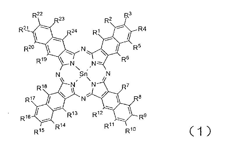
一般式(1)中、R1~R24は、独立して、水素原子または置換基を表す。置換基は、特定の置換基に限定されない。置換基は、重水素原子、ハロゲン原子、アルキル基(シクロアルキル基、ビシクロアルキル基、トリシクロアルキル基を含む)、アルケニル基(シクロアルケニル基、ビシクロアルケニル基を含む)、アルキニル基、アリール基、複素環基(ヘテロ環基といってもよい)、シアノ基、ヒドロキシ基、ニトロ基、カルボキシ基、アルコキシ基、アリールオキシ基、シリルオキシ基、ヘテロ環オキシ基、アシルオキシ基、カルバモイルオキシ基、アルコキシカルボニルオキシ基、アリールオキシカルボニルオキシ基、アミノ基(アニリノ基を含む)、アンモニオ基、アシルアミノ基、アミノカルボニルアミノ基、アルコキシカルボニルアミノ基、アリールオキシカルボニルアミノ基、スルファモイルアミノ基、アルキルスルホニルアミノ基、アリールスルホニルアミノ基、メルカプト基、アルキルチオ基、アリールチオ基、ヘテロ環チオ基、スルファモイル基、スルホ基、アルキルスルフィニル基、アリールスルフィニル基、アルキルスルホニル基、アリールスルホニル基、アシル基、アリールオキシカルボニル基、アルコキシカルボニル基、カルバモイル基、アリールアゾ基、ヘテロ環アゾ基、イミド基、ホスフィノ基、ホスフィニル基、ホスフィニルオキシ基、ホスフィニルアミノ基、ホスホノ基、シリル基、ヒドラジノ基、ウレイド基、ボロン酸基(-B(OH)2)、ホスファト基(-OPO(OH)2)、スルファト基(-OSO3H)、または、その他の公知の置換基であり得る。
上述の一般式(1)で表されるスズナフタロシアニンとしては、市販されている製品を用いることができる。あるいは、上述の一般式(1)で表されるスズナフタロシアニンは、例えば特開2010-232410号公報に示されているように、下記の一般式(2)で表されるナフタレン誘導体を出発原料として合成することができる。一般式(2)中のR25~R30は、一般式(1)におけるR1~R24と同様の置換基であり得る。

上述の一般式(1)で表されるスズナフタロシアニンにおいて、分子の凝集状態の制御のし易さの観点から、R1~R24のうち、8個以上が水素原子または重水素原子であると有益であり、R1~R24のうち、16個以上が水素原子または重水素原子であるとより有益であり、全てが水素原子または重水素原子であるとさらに有益である。さらに、以下の式(3)で表されるスズナフタロシアニンは、合成の容易さの観点で有利である。

上述の一般式(1)で表されるスズナフタロシアニンは、概ね200nm以上1100nm以下の波長帯域に吸収を有する。スズナフタロシアニンの吸収ピークは、波長が概ね940nmの位置であり得る。なお、上述の式(3)で表されるスズナフタロシアニンは、図5に示すように、波長が概ね870nmの位置に吸収ピークを有する。図5は、上述の式(3)で表されるスズナフタロシアニンを含む光電変換層における吸収スペクトルの一例である。式(3)で表されるスズナフタロシアニンを含む光電変換層の、波長900nmにおける量子効率は、シリコンの10倍程度であり得る。吸収スペクトルの測定においては、石英基板上に光電変換層(厚さ:30nm)が積層されたサンプルを用いている。
図5からわかるように、スズナフタロシアニンを含む材料から形成された光電変換層は、近赤外領域に吸収を有する。すなわち、光電変換層23Aを構成する材料として、スズナフタロシアニンを含む材料を選択することにより、近赤外線を検出可能な光センサを実現し得る。本開示の実施形態によれば、検出を行いたい波長域に応じて適切な材料を用いることにより、所望の波長域に感度を有する光センサを実現し得る。例えば、有機p型半導体化合物の一例であるP3HT(ポリ(3-ヘキシルチオフェン-2,5-ジイル))は、波長550nmに吸収ピークを有しており、銅フタロシアニンは、波長620nmおよび波長700nmに吸収ピークを有する。
光を吸収することによって電荷を発生させることができれば、光電変換層23Aを形成するための材料に特に制限はない。光電変換層23Aは、後述する有機p型半導体(化合物)から形成されていてもよいし、後述する有機n型半導体(化合物)から形成されていてもよい。あるいは、有機p型半導体(化合物)と有機n型半導体(化合物)とを組み合わせて、光電変換層23Aを形成してもよい。光電変換層23Aが、アモルファスシリコンなどの無機半導体材料を含んでいてもよい。光電変換層23Aが、有機材料から構成される層と無機材料から構成される層とを含んでいてもよい。
図6は、上述の一般式(1)で表されるスズナフタロシアニンを含む有機半導体材料を用いて形成した光電変換層を有する光検出素子の構成の一例を示す。図6に示す光検出素子10Bの誘電体構造2Bは、正孔ブロッキング層20h、光電変換層23Bおよび電子ブロッキング層20eを含む。図6に例示する構成において、正孔ブロッキング層20hは、第1電極21と光電変換層23Bとの間に配置されており、電子ブロッキング層20eは、光電変換層23Bと第2電極22との間に配置されている。
光電変換層23Bは、p型半導体およびn型半導体の少なくとも一方を含む。図6に例示する構成では、光電変換層23Bは、p型半導体層230pと、n型半導体層230nと、p型半導体層230pとn型半導体層230nとの間に挟まれた混合層230hとを有する。p型半導体層230pは、正孔ブロッキング層20hと混合層230hとの間に配置されており、光電変換層および/または正孔輸送層としての機能を有する。n型半導体層230nは、混合層230hと電子ブロッキング層20eとの間に配置されており、光電変換層および/または電子輸送層としての機能を有する。後述するように、混合層230hは、p型半導体およびn型半導体を含む層である。
p型半導体層230pおよびn型半導体層230nは、それぞれ、有機p型半導体および有機n型半導体を含む。光電変換層23Bが、上述の一般式(1)で表されるスズナフタロシアニンを含む有機光電変換材料と、有機p型半導体および有機n型半導体の少なくとも一方とを含んでいてもよい。
有機p型半導体(化合物)は、ドナー性有機半導体(化合物)であり、主に正孔輸送性有機化合物に代表され、電子を供与しやすい性質がある有機化合物をいう。さらに詳しくは、有機p型半導体(化合物)は、2つの有機材料を接触させて用いたときにイオン化ポテンシャルの小さい方の有機化合物をいう。したがって、ドナー性有機化合物としては、電子供与性のある有機化合物であればいずれの有機化合物も使用可能である。例えば、トリアリールアミン化合物、ベンジジン化合物、ピラゾリン化合物、スチリルアミン化合物、ヒドラゾン化合物、トリフェニルメタン化合物、カルバゾール化合物、ポリシラン化合物、P3HTなどのチオフェン化合物、銅フタロシアニンなどのフタロシアニン化合物、シアニン化合物、メロシアニン化合物、オキソノール化合物、ポリアミン化合物、インドール化合物、ピロール化合物、ピラゾール化合物、ポリアリーレン化合物、縮合芳香族炭素環化合物(ナフタレン誘導体、アントラセン誘導体、フェナントレン誘導体、テトラセン誘導体、ピレン誘導体、ペリレン誘導体、フルオランテン誘導体)、含窒素ヘテロ環化合物を配位子として有する金属錯体などを用いることができる。なお、ドナー性有機半導体は、これらに限らず、上述したように、n型(アクセプター性)化合物として用いた有機化合物よりもイオン化ポテンシャルの小さい有機化合物であればドナー性有機半導体として用い得る。上述のスズナフタロシアニンは、有機p型半導体材料の一例である。
有機n型半導体(化合物)は、アクセプター性有機半導体(化合物)であり、主に電子輸送性有機化合物に代表され、電子を受容しやすい性質がある有機化合物をいう。さらに詳しくは、有機n型半導体(化合物)は、2つの有機化合物を接触させて用いたときに電子親和力の大きい方の有機化合物をいう。したがって、アクセプター性有機化合物としては、電子受容性のある有機化合物であればいずれの有機化合物も使用可能である。例えば、フラーレン、フェニルC61酪酸メチルエステル(PCBM)などのフラーレン誘導体、縮合芳香族炭素環化合物(ナフタレン誘導体、アントラセン誘導体、フェナントレン誘導体、テトラセン誘導体、ピレン誘導体、ペリレン誘導体、フルオランテン誘導体)、窒素原子、酸素原子、硫黄原子を含有する5ないし7員のヘテロ環化合物(例えばピリジン、ピラジン、ピリミジン、ピリダジン、トリアジン、キノリン、キノキサリン、キナゾリン、フタラジン、シンノリン、イソキノリン、プテリジン、アクリジン、フェナジン、フェナントロリン、テトラゾール、ピラゾール、イミダゾール、チアゾール、オキサゾール、インダゾール、ベンズイミダゾール、ベンゾトリアゾール、ベンゾオキサゾール、ベンゾチアゾール、カルバゾール、プリン、トリアゾロピリダジン、トリアゾロピリミジン、テトラザインデン、オキサジアゾール、イミダゾピリジン、ピラリジン、ピロロピリジン、チアジアゾロピリジン、ジベンズアゼピン、トリベンズアゼピンなど)、ポリアリーレン化合物、フルオレン化合物、シクロペンタジエン化合物、シリル化合物、ペリレンテトラカルボキシルジイミド化合物(PTCDI)、含窒素ヘテロ環化合物を配位子として有する金属錯体などを用いることができる。なお、これらに限らず、上述したように、p型(ドナー性)有機化合物として用いた有機化合物よりも電子親和力の大きな有機化合物であればアクセプター性有機半導体として用い得る。
図6に例示するように、誘電体構造2Bが、p型半導体層230pとn型半導体層230nとを含む光電変換層23Bを有すると、光電変換によって生成された正孔および電子を互いに分離させやすい。そのため、p型半導体層230pとn型半導体層230nとを含む光電変換層23Bを用いることにより、電荷分離の効率が向上し、入射光強度の変化に対して、より大きな誘電率の変化が得られる。
混合層230hは、例えば、p型半導体およびn型半導体を含むバルクヘテロ接合構造層であり得る。バルクへテロ接合構造を有する層として混合層230hを形成する場合、上述の一般式(1)で表されるスズナフタロシアニンをp型半導体材料として用い得る。n型半導体材料としては、例えば、フラーレンおよび/またはフラーレン誘導体を用いることができる。バルクへテロ接合構造は、特許第5553727号公報において詳細に説明されている。参考のため、特許第5553727号公報の開示内容の全てを本明細書に援用する。
(正孔ブロッキング層)
正孔ブロッキング層20hを形成するための材料としては、n型半導体あるいは電子輸送性有機化合物を用いることができる。このような材料の例は、C60およびC70などのフラーレン、インデンーC60ビス付加物(ICBA)などのフラーレン誘導体、カーボンナノチューブおよびその誘導体、OXD-7(1,3-ビス(4-tert-ブチルフェニル-1,3,4-オキサジアゾリル)フェニレン)などのオキサジアゾール誘導体、アントラキノジメタン誘導体、ジフェニルキノン誘導体、バソクプロイン(BCP)、バソフェナントロリンおよびその誘導体、ジスチリルアリーレン誘導体、トリアゾール化合物、シロール化合物、トリス(8-ヒドロキシキノリナート)アルミニウム錯体、ビス(4-メチル-8-キノリナート)アルミニウム錯体、アセチルアセトネート錯体、銅フタロシアニン、3,4,9,10-ペリレンテトラカルボン酸二無水物(PTCDA)、Alqなどの有機物もしくは有機-金属化合物、または、MgAg、MgOなどの無機物などである。正孔ブロッキング層20hを形成するための材料は、光電変換層23A(または光電変換層23Bにおけるp型半導体層230p)を構成する材料のイオン化ポテンシャルを考慮して上記の材料から選択され得る。
正孔ブロッキング層20hを形成するための材料としては、n型半導体あるいは電子輸送性有機化合物を用いることができる。このような材料の例は、C60およびC70などのフラーレン、インデンーC60ビス付加物(ICBA)などのフラーレン誘導体、カーボンナノチューブおよびその誘導体、OXD-7(1,3-ビス(4-tert-ブチルフェニル-1,3,4-オキサジアゾリル)フェニレン)などのオキサジアゾール誘導体、アントラキノジメタン誘導体、ジフェニルキノン誘導体、バソクプロイン(BCP)、バソフェナントロリンおよびその誘導体、ジスチリルアリーレン誘導体、トリアゾール化合物、シロール化合物、トリス(8-ヒドロキシキノリナート)アルミニウム錯体、ビス(4-メチル-8-キノリナート)アルミニウム錯体、アセチルアセトネート錯体、銅フタロシアニン、3,4,9,10-ペリレンテトラカルボン酸二無水物(PTCDA)、Alqなどの有機物もしくは有機-金属化合物、または、MgAg、MgOなどの無機物などである。正孔ブロッキング層20hを形成するための材料は、光電変換層23A(または光電変換層23Bにおけるp型半導体層230p)を構成する材料のイオン化ポテンシャルを考慮して上記の材料から選択され得る。
第1電極21側から光電変換層23B(または光電変換層23A)に光が入射するような構成においては、正孔ブロッキング層20hにおいて、検出を行いたい波長域の透過率が高いと有益である。例えば、正孔ブロッキング層20hの厚さを小さくしてもよい。正孔ブロッキング層20hは、例えば、5nm以上50nm以下の範囲の厚さを有し得る。
(電子ブロッキング層)
電子ブロッキング層20eを形成するための材料としては、p型半導体あるいは正孔輸送性有機化合物を用いることができる。このような材料の例は、TPD(N,N’-ビス(3-メチルフェニル)-(1,1’-ビフェニル)-4,4’-ジアミン)、α-NPD(4,4’-ビス[N-(ナフチル)-N-フェニル-アミノ]ビフェニル)などの芳香族ジアミン化合物、オキサゾール、オキサジアゾール、トリアゾール、イミダゾール、イミダゾロン、スチルベン誘導体、ピラゾリン誘導体、テトラヒドロイミダゾール、ポリアリールアルカン、ブタジエン、m-MTDATA(4,4’,4”-トリス(N-(3-メチルフェニル)N-フェニルアミノ)トリフェニルアミン)、ぺリレン、ならびに、ポルフィン、テトラフェニルポルフィン銅、フタロシアニン、銅フタロシアニンおよびチタニウムフタロシアニンオキサイドなどのポリフィリン化合物、トリアゾール誘導体、オキサジザゾール誘導体、イミダゾール誘導体、ポリアリールアルカン誘導体、ピラゾリン誘導体、ピラゾロン誘導体、フェニレンジアミン誘導体、アニールアミン誘導体、アミノ置換カルコン誘導体、オキサゾール誘導体、スチリルアントラセン誘導体、フルオレノン誘導体、ヒドラゾン誘導体、シラザン誘導体などである。あるいは、電子ブロッキング層20eを形成するための材料として、フェニレンビニレン、フルオレン、カルバゾール、インドール、ピレン、ピロール、ピコリン、チオフェン、アセチレン、ジアセチレンなどの重合体、または、これらの誘導体を用いることができる。電子ブロッキング層20eを形成するための材料は、光電変換層23A(または光電変換層23Bにおけるn型半導体層230n)を構成する材料の電子親和力を考慮して上記の材料から選択され得る。
電子ブロッキング層20eを形成するための材料としては、p型半導体あるいは正孔輸送性有機化合物を用いることができる。このような材料の例は、TPD(N,N’-ビス(3-メチルフェニル)-(1,1’-ビフェニル)-4,4’-ジアミン)、α-NPD(4,4’-ビス[N-(ナフチル)-N-フェニル-アミノ]ビフェニル)などの芳香族ジアミン化合物、オキサゾール、オキサジアゾール、トリアゾール、イミダゾール、イミダゾロン、スチルベン誘導体、ピラゾリン誘導体、テトラヒドロイミダゾール、ポリアリールアルカン、ブタジエン、m-MTDATA(4,4’,4”-トリス(N-(3-メチルフェニル)N-フェニルアミノ)トリフェニルアミン)、ぺリレン、ならびに、ポルフィン、テトラフェニルポルフィン銅、フタロシアニン、銅フタロシアニンおよびチタニウムフタロシアニンオキサイドなどのポリフィリン化合物、トリアゾール誘導体、オキサジザゾール誘導体、イミダゾール誘導体、ポリアリールアルカン誘導体、ピラゾリン誘導体、ピラゾロン誘導体、フェニレンジアミン誘導体、アニールアミン誘導体、アミノ置換カルコン誘導体、オキサゾール誘導体、スチリルアントラセン誘導体、フルオレノン誘導体、ヒドラゾン誘導体、シラザン誘導体などである。あるいは、電子ブロッキング層20eを形成するための材料として、フェニレンビニレン、フルオレン、カルバゾール、インドール、ピレン、ピロール、ピコリン、チオフェン、アセチレン、ジアセチレンなどの重合体、または、これらの誘導体を用いることができる。電子ブロッキング層20eを形成するための材料は、光電変換層23A(または光電変換層23Bにおけるn型半導体層230n)を構成する材料の電子親和力を考慮して上記の材料から選択され得る。
第2電極22側から光電変換層23B(または光電変換層23A)に光が入射するような構成においては、電子ブロッキング層20eにおいて、検出を行いたい波長域の透過率が高いと有益である。例えば、電子ブロッキング層20eの厚さを小さくしてもよい。電子ブロッキング層20eは、例えば、5nm以上50nm以下の範囲の厚さを有し得る。
(光検出素子の他の構成例)
第1電極21、光電変換層(光電変換層23Aまたは23B)および第2電極22の材料として、適切な材料の組み合わせを選択することにより、正孔ブロッキング層20hおよび電子ブロッキング層20eの一方を省略することが可能である。以下、このような構成の例を説明する。
第1電極21、光電変換層(光電変換層23Aまたは23B)および第2電極22の材料として、適切な材料の組み合わせを選択することにより、正孔ブロッキング層20hおよび電子ブロッキング層20eの一方を省略することが可能である。以下、このような構成の例を説明する。
図7は、第1電極21と第2電極22との間に正孔ブロッキング層20hおよび光電変換層23Cが配置された光検出素子における例示的なエネルギー図である。図示するように、この例では、第2電圧が印加される第2電極22に、光電変換層23Cが隣接している。つまり、図7は、上述の電子ブロッキング層20eが省略された構成の例を示している。ここでは、光電変換層23Cが、p型半導体層230pおよびn型半導体層230nのヘテロ接合構造を有する例を説明する。もちろん、光電変換層23Cは、バルクヘテロ接合構造を有する層であっても構わない。
図7に例示する構成では、図2および図3を参照して説明した光検出素子10Aと同様に、正孔ブロッキング層20hによって、第1電極21への光電変換層23Cからの正孔の移動が抑制される。また、図7に例示する構成では、正孔ブロッキング層20hのLUMOと第1電極21のフェルミ準位との間の差が大きく、第1電極21と正孔ブロッキング層20hとの間に、電子に対するポテンシャル障壁が形成されている。このポテンシャル障壁により、正孔ブロッキング層20hへの第1電極21からの電子の移動が抑制される。換言すれば、電子ブロッキング層を用いることなく、第1電極21から正孔ブロッキング層20hへの電子の輸送が抑制されている。
光電変換層(ここでは光電変換層23C)と電極(ここでは第2電極22)とが隣接して配置された構成では、電極の仕事関数と、電極に隣接する有機膜のイオン化ポテンシャルとの間の差が大きければ、電極からの有機膜への正孔の進入が起こりにくいことが知られている。図7に例示する構成では、光電変換層23Cのイオン化ポテンシャルが第2電極22の仕事関数よりも大きく、かつ、光電変換層23CのHOMOと、第2電極22のフェルミ準位との間の差が比較的大きいので、光電変換層23Cと第2電極22との間のポテンシャル障壁によって、第2電極22からの光電変換層23Cへの正孔の注入が抑制される。
このように、光電変換によって生じた正および負の電荷のうちの一方(ここでは正孔)の電極(ここでは第1電極21)への移動を抑制することによっても、光電変換によって生じた電荷を光電変換層23C中に留め得る。つまり、電子ブロッキング層20eを設けなくても、光検出素子の各部におけるエネルギーの相対的な関係が図7に示す関係となるように、第1電極21、正孔ブロッキング層20h、光電変換層23Cおよび第2電極22の材料を適切に選択することによって、光の照射に対する誘電率変化を実現し得る。
光検出素子の各部におけるエネルギーの相対的な関係が図7に示す関係を満たし得る材料の組み合わせとして、以下の組み合わせを例示することができる。
第1電極21:ITO(WF:4.7eV)
正孔ブロッキング層20h:ICBA(IP:6.5eV、EA:3.7eV)
p型半導体層230p:銅フタロシアニン(IP:5.2eV、EA:3.5eV)
n型半導体層230n:C60(IP:6.2eV、EA:4.5eV)
第2電極22:Al(WF:4.2eV)
図8は、このような組み合わせにおいて実現され得る、エネルギーの相対的な関係を模式的に示す。図8中、矢印φ1は、正孔ブロッキング層20hと第1電極21との間の、電子に対するポテンシャル障壁を表し、矢印φ2は、n型半導体層230nと第2電極22との間の、正孔に対するポテンシャル障壁を表す。矢印φ3は、p型半導体層230pと正孔ブロッキング層20hとの間の、正孔に対するポテンシャル障壁を表す。言うまでもないが、上記組み合わせは、あくまでも例であり、例えば、p型半導体層230pの材料として例示されている銅フタロシアニンに代えて、P3HT、スズナフタロシアニンなどを用いてももちろん構わない。
図9は、第1電極21と第2電極22との間に光電変換層23Cおよび電子ブロッキング層20eが配置された光検出素子における例示的なエネルギー図である。図示するように、この例では、第1電圧が印加される第1電極21に、光電変換層23Cが隣接している。つまり、図9は、上述の正孔ブロッキング層20hが省略された構成の例を示している。
図示する例では、図2および図3を参照して説明した光検出素子10Aと同様に、電子ブロッキング層20eによって、第2電極22への光電変換層23Cからの電子の移動が抑制される。また、図9に例示する構成では、電子ブロッキング層20eのHOMOと第2電極22のフェルミ準位との間の差が大きく、電子ブロッキング層20eと第2電極22との間に、正孔に対するポテンシャル障壁が形成されている。このポテンシャル障壁により、電子ブロッキング層20eへの第2電極22からの正孔の移動が抑制される。換言すれば、正孔ブロッキング層を用いることなく、第2電極22から電子ブロッキング層20eへの正孔の輸送が抑制されている。
電極(ここでは第1電極21)と光電変換層(ここでは光電変換層23C)とが隣接して配置された構成では、電極の仕事関数と、電極に隣接する有機膜の電子親和力との間の差が大きければ、電極からの有機膜への電子の注入が起こりにくい。図9に例示する構成では、光電変換層23Cの電子親和力が第1電極21の仕事関数よりも小さく、かつ、第1電極21のフェルミ準位と、光電変換層23CのLUMOとの間の差が比較的大きい。そのため、第1電極21と光電変換層23Cとの間に、ポテンシャル障壁が形成されている。このポテンシャル障壁により、第1電極21からの光電変換層23Cへの電子の注入が抑制される。このように、正孔ブロッキング層20hを設けることなく、光検出素子の各部におけるエネルギーの相対的な関係が図9に示す関係となるように、第1電極21、光電変換層23C、電子ブロッキング層20eおよび第2電極22の材料を適切に選択することによって、光の照射に対する誘電率変化を実現することも可能である。
光検出素子の各部におけるエネルギーの相対的な関係が図9に示す関係となるような、第1電極21、光電変換層23C、電子ブロッキング層20eおよび第2電極22の材料の組み合わせとして、以下の組み合わせを例示することができる。
第1電極21:ITO(WF:4.7eV)
p型半導体層230p:銅フタロシアニン(IP:5.2eV、EA:3.5eV)
n型半導体層230n:C60(IP:6.2eV、EA:4.5eV)
電子ブロッキング層20e:ぺリレン(IP:5.3eV、EA:2.3eV)
第2電極22:Al(WF:4.2eV)
図10は、このような組み合わせにおいて実現され得る、エネルギーの相対的な関係を模式的に示す。図10中、矢印φ5は、第1電極21とp型半導体層230pとの間の、電子に対するポテンシャル障壁を表し、矢印φ6は、電子ブロッキング層20eと第2電極22との間の、正孔に対するポテンシャル障壁を表す。矢印φ7は、n型半導体層230nと電子ブロッキング層20eとの間の、電子に対するポテンシャル障壁を表す。以下に例示されている銅フタロシアニンに代えて、P3HT、スズナフタロシアニンなどを用いてもよいし、電子ブロッキング層20eの材料として例示されているぺリレンに代えて、銅フタロシアニンを用いてもよい。
このように、正孔ブロッキング層20hおよび電子ブロッキング層20eのいずれかが省略された光検出素子によっても、光電変換によって生成された電荷の電極への移動を抑制し得る。換言すれば、より簡易な構造により、正孔ブロッキング層20hおよび電子ブロッキング層20eの両方を有する光検出素子と同様の効果を得ることが可能である。ここで、誘電体構造に正孔ブロッキング層20hおよび電子ブロッキング層20eのいずれか一方が配置された光検出素子では、電圧の印加によって2つの電極のうちのいずれを高電位とするかに応じて、ブロッキング層(正孔ブロッキング層20hまたは電子ブロッキング層20e)を介在させるべき位置が決まることに注意すべきである。
(光センサの第2の実施形態)
光電変換によって生成された電荷の電極への移動を抑制するという観点から、正孔ブロッキング層20hおよび/または電子ブロッキング層20eに代えて、正孔も電子も通さない絶縁層を用いてもよい。以下、光電変換層と電極との間に絶縁層を配置した構成の例を説明する。
光電変換によって生成された電荷の電極への移動を抑制するという観点から、正孔ブロッキング層20hおよび/または電子ブロッキング層20eに代えて、正孔も電子も通さない絶縁層を用いてもよい。以下、光電変換層と電極との間に絶縁層を配置した構成の例を説明する。
図11は、本開示の第2の実施形態に係る光センサの例示的な構成の概略を示す。図11に示す光センサ100Cは、第1電極21および第2電極22の間に配置された誘電体構造2Cを含む光検出素子10Cと、電圧供給回路12とを有する。誘電体構造2Cは、絶縁層29aおよび絶縁層29bを有する。図示するように、絶縁層29aは、第1電極21と光電変換層23Cとの間に配置されている。絶縁層29bは、光電変換層23Cと第2電極22との間に配置されている。
図12は、光検出素子10Cにおける例示的なエネルギー図である。図12中、3つ並ぶ矩形のうち、一番左の矩形の底辺は、絶縁層29aの価電子帯の上端を表し、底辺に対向する辺は、伝導帯の底を表す。同様に、図12中、一番右側の矩形は、絶縁層29bにおける価電子帯の上端および伝導帯の底のそれぞれにおけるエネルギー準位の高さを模式的に示している。以下では、価電子帯の上端と真空準位との間の差、および、伝導帯の底と真空準位との間の差を、それぞれ、VBおよびCBで表すことがある。
第1電極21と光電変換層23Cとの間に絶縁層29aを配置することにより、第1電極21と第2電極22との間に電圧が印加された状態であっても、第1電極21と光電変換層23Cとの間における電荷の移動を抑制できる。また、第2電極22と光電変換層23Cとの間に絶縁層29bを配置することにより、第2電極22と光電変換層23Cとの間における電荷の移動を抑制できる。したがって、光電変換によって生じた電荷は、電極(第1電極21および/または第2電極22)への移動が抑制され、誘電体構造2Cの誘電率の変化に寄与する電荷として利用できる。本明細書における「絶縁層」は、正および負の両方の電荷の移動を、外部から印加された電場の方向に関わらずブロックする点で、上述の正孔ブロッキング層20hおよび電子ブロッキング層20eと区別される。別の言い方をすれば、本明細書における「絶縁層」は、正および負の両方の電荷に関して、電極から光電変換層への移動、および、光電変換層から電極への移動を抑制する。
絶縁層29aおよび29bを形成するための材料としては、例えば、SiO2、Al2O3、ZrO2、HfO2、Y2O3などの酸化物、または、ポリメタクリル酸メチル(PMMA)、ポリイミド、パリレン(登録商標)、ポリスチレンなどの樹脂などを用いることができる。絶縁層29aおよび29bを構成する材料は、同一であってもよいし、互いに異なっていてもよい。絶縁層29aおよび/または絶縁層29bとして、シリコン半導体において一般的に用いられるシリコン酸窒化膜(SiON膜)を適用してもよい。いわゆる高誘電率材料(high-k材料とも呼ばれ、典型的には比誘電率が3.9超である)を用いて絶縁層29aおよび/または絶縁層29bを形成すると有益である。絶縁層29aおよび絶縁層29bの厚さは、絶縁層29aおよび絶縁層29bの電気伝導率に応じて適宜設定し得る。
図11および図12に例示する構成では、第1電極21と光電変換層23Cとの間に、絶縁層29aが配置されている。また、光電変換層23Cと第2電極22との間に、絶縁層29bが配置されている。したがって、光センサ100Cの動作時、第1電極21および第2電極22のいずれを高電位としてもよい。つまり、図11に例示するような構成によれば、第1電極21の材料および第2電極22の材料に対する制約が小さいという利点も得られる。例えば、第2電極22が透明電極である場合には、第2電極22の材料として、ITO、IZO、AZO、FTO、SnO2、TiO2、ZnO2などの透明導電性酸化物(TCO)、あるいは、カーボンナノチューブ、グラフェンなどを用いることができる。第1電極21が透明電極である場合、第2電極22の材料として、Al、TiN、Cu、TaNなどを用いてもよい。第1電極21についても、第2電極22と同様の材料を用い得る。例えば、第1電極21の材料として、Al、TiN、Cu、TaN、ITOなどを用いることができる。
(光検出素子の他の構成例)
以下に説明するように、第1電極21、光電変換層23C(または光電変換層23A、23B)および第2電極22の材料として適切な材料の組み合わせを選択することにより、絶縁層29aおよび29bの一方を省略することが可能である。
以下に説明するように、第1電極21、光電変換層23C(または光電変換層23A、23B)および第2電極22の材料として適切な材料の組み合わせを選択することにより、絶縁層29aおよび29bの一方を省略することが可能である。
図13は、第1電極21と第2電極22との間に絶縁層29aおよび光電変換層23Cが配置された光検出素子における例示的なエネルギー図である。図示するように、この例では、第2電圧が印加される第2電極22に、光電変換層23Cが隣接している。つまり、図13は、上述の絶縁層29bが省略された構成の例を示している。
図13に例示する構成では、光電変換層23Cから第1電極21への正孔の移動、および、第1電極21から光電変換層23Cへの電子の移動が、絶縁層29aによって抑制される。また、この例では、光電変換層23Cのイオン化ポテンシャルが第2電極22の仕事関数よりも大きく設定されている。したがって、第2電極22から光電変換層23Cへの正孔の注入は、光電変換層23Cと第2電極22との間のポテンシャル障壁によって抑制される。したがって、光電変換によって生じた電荷(例えば正孔)の一部を光電変換層23Cに留めて、光電変換層23Cの誘電率の変化に寄与する電荷として利用し得る。このように、光検出素子の各部におけるエネルギーの相対的な関係が図13に示す関係となるように、第1電極21、絶縁層29a、光電変換層23Cおよび第2電極22の材料を適切に選択することにより、光電変換層23Cと第2電極22との間に絶縁層29bを設けることなく、光電変換によって生成された電荷の電極への移動を抑制することも可能である。
光検出素子の各部におけるエネルギーの相対的な関係が図13に示す関係を満たし得る材料の組み合わせとして、以下の組み合わせを例示することができる。
第1電極21:ITO(WF:4.7eV)
絶縁層29a:Al2O3(VB:10.0eV、CB:1.2eV)
p型半導体層230p:銅フタロシアニン(IP:5.2eV、EA:3.5eV)
n型半導体層230n:C60(IP:6.2eV、EA:4.5eV)
第2電極22:Al(WF:4.2eV)
図14は、このような組み合わせにおいて実現され得る、エネルギーの相対的な関係を模式的に示す。第2電極22の材料としては、仕事関数が概ね4.1eV以上4.3eV以下の範囲にある金属を用い得る。したがって、以下に例示されているAlに代えて、Ti、Ta、Agなどを用いてもよい。第2電極22に隣接するn型半導体層230nの材料としては、イオン化ポテンシャルが概ね5eV以上の材料を用いればよい。また、絶縁層29aの材料として例示されているAl2O3に代えて、SiO2、ZrO2、HfO2、Y2O3などを用いてもよい。
図15は、第1電極21と第2電極22との間に光電変換層23Cおよび絶縁層29bが配置された光検出素子における例示的なエネルギー図である。図示するように、この例では、第1電圧が印加される第1電極21に、光電変換層23Cが隣接している。つまり、図15は、上述の絶縁層29aが省略された構成の例を示している。
図15に例示する構成では、光電変換層23Cから第2電極22への電子の移動、および、第2電極22から光電変換層23Cへの正孔の移動が、絶縁層29bによってブロックされる。また、この例では、光電変換層23Cの電子親和力が第1電極21の仕事関数よりも小さく設定されている。したがって、第1電極21から光電変換層23Cへの電子の注入は、第1電極21と光電変換層23Cとの間のポテンシャル障壁によって抑制される。したがって、このような構成によっても、光電変換によって生じた電荷(例えば電子)の一部を光電変換層23Cに留めて、光電変換層23Cの誘電率の変化に寄与する電荷として利用し得る。このように、光検出素子の各部におけるエネルギーの相対的な関係が図15に示す関係となるように、第1電極21、光電変換層23C、絶縁層29bおよび第2電極22の材料を適切に選択することにより、第1電極21と光電変換層23Cとの間に絶縁層29aを設けることなく、光電変換によって生成された電荷の電極への移動を抑制し得る。
光検出素子の各部におけるエネルギーの相対的な関係が図15に示す関係を満たし得る材料の組み合わせとして、以下の組み合わせを例示することができる。
第1電極21:Au(WF:4.9eV)
p型半導体層230p:銅フタロシアニン(IP:5.2eV、EA:3.5eV)
n型半導体層230n:C60(IP:6.2eV、EA:4.5eV)
絶縁層29b:Al2O3(VB:10.0eV、CB:1.2eV)
第2電極22:ITO(WF:4.7eV)
図16は、このような組み合わせにおいて実現され得る、エネルギーの相対的な関係を模式的に示す。第1電極21の材料としては、仕事関数が概ね4.8eV以上の金属を用い得る。例えば、以下に例示されているAuに代えて、Pt、Ni、ITOなどを用いてもよい。
p型半導体層230p:銅フタロシアニン(IP:5.2eV、EA:3.5eV)
n型半導体層230n:C60(IP:6.2eV、EA:4.5eV)
絶縁層29b:Al2O3(VB:10.0eV、CB:1.2eV)
第2電極22:ITO(WF:4.7eV)
図16は、このような組み合わせにおいて実現され得る、エネルギーの相対的な関係を模式的に示す。第1電極21の材料としては、仕事関数が概ね4.8eV以上の金属を用い得る。例えば、以下に例示されているAuに代えて、Pt、Ni、ITOなどを用いてもよい。
次に、実施例を参照しながら、光照射による、光電変換層における誘電率の変化の一例を説明する。図17は、誘電率の変化の測定に使用した光検出素子の構造を模式的に示す。以下の手順により、図17に示す構造を有する光検出素子10Dを製作した。
まず、ガラス基板2GLを用意した。次に、スパッタリングを用いてITOをガラス基板2GL上に堆積することにより、第2電極22としてのITO電極(厚さ:50nm)を形成した。次に、原子層堆積法(Atomic Layer Deposition(ALD))を用いて、第2電極22上に、絶縁層29bとしてのHfO2層(厚さ:30nm)を形成した。さらに、スズナフタロシアニンとC60とを共蒸着することにより、光電変換層23Dとしての共蒸着層(厚さ:150nm)を絶縁層29b上に形成した。
次に、ALDを用いて、光電変換層23D上に、絶縁層29aとしてのAl2O3層(厚さ:30nm)を形成した。その後、スパッタリングを用いてAlを絶縁層29a上に堆積することにより、第1電極21としてのAl電極(厚さ:80nm)を形成した。以上の工程により、図17に示す構造の光検出素子10Dを得た。なお、ガラス基板2GLの法線方向からみたときの光電変換層23Dの形状は、1mm角の矩形状であった。
ここでは、LED光源(波長:940nm、定格消費電力:およそ70mW)を用いた。図17に模式的に示すように、第1電極21および第2電極22に測定機300を接続して、第1電極21および第2電極22の間に4Vの電位差を与えた。この状態で、第1電極21および第2電極22の間の誘電体構造2Dにおける容量値を測定した。容量値の測定には、Keysight社製、半導体デバイスパラメータアナライザ、B1500A(測定周波数:1kHz、振幅:0.1V)を使用し、測定機のプローブのLOW側を第1電極21に接触させ、HIGH側を第2電極22に接触させた状態で測定を行った。
図18は、誘電体構造2Dの容量値の測定結果を示す。図18中、白抜きの四角形(□)は、光電変換層23Dに光が照射されていない状態(LED光源:消灯、暗状態)についての容量値の測定結果を示す。白抜きの三角形(△)は、光電変換層23Dに光が照射された状態(LED光源:点灯)についての容量値の測定結果を示す。図18に示すように、光が照射されていない状態の容量値は約6.3μFであり、光が照射された状態の容量値は約2μFである。したがって、この例では、誘電体構造2Dの容量値は、光電変換層23Dへの光の照射により、暗状態と比較しておよそ3倍の向上を示している。
さらに、第1電極21および第2電極22に4Vの電位差を与えた状態で、1秒ごとにLED光源の点灯および消灯を切り替え、誘電体構造2Dにおける容量値の変化を測定した。図18中、白抜きの菱形(◇)は、1秒ごとにLED光源の点灯および消灯を切り替えたときの容量値の測定結果を示す。図18に示すように、光電変換層23Dへの光の入射により、誘電体構造2Dの容量値が、速やかな上昇を示した。また、LED光源を消灯すると、誘電体構造2Dの容量値が、速やかに低下した。
このように、本開示の実施形態によれば、照度の変化に応じて電極間の容量値が変化する光センサを実現し得る。
(デバイス構造の具体例)
以下、図面を参照しながら、光の照射による誘電率の変化に対応した信号を生成可能な光検出素子におけるデバイス構造の具体例を説明する。
以下、図面を参照しながら、光の照射による誘電率の変化に対応した信号を生成可能な光検出素子におけるデバイス構造の具体例を説明する。
図19は、光検出素子のデバイス構造の一例を示す。図19に示す光検出素子10Eは、基板2に支持されている。基板2としては、例えば、表面に酸化膜を有するシリコン基板、ガラス基板、ポリイミド基板などを用い得る。図示する例では、基板2上に第2電極22が配置されている。
図19に例示する構成において、第1電極21と第2電極22との間に配置された誘電体構造2Eは、障壁層B1、B2と、光電変換層23Aとを有する。第1電極21と光電変換層23Aとの間に配置された障壁層B1は、上述した正孔ブロッキング層20hまたは絶縁層29aのいずれかであり得る。すなわち、障壁層B1は、少なくとも、光電変換層(ここでは光電変換層23A)から第1電極21への正孔の輸送を抑制する機能を有する層である。光電変換層23Aと第2電極22との間に配置された障壁層B2は、上述した電子ブロッキング層20eまたは絶縁層29bのいずれかであり得る。すなわち、障壁層B2は、少なくとも、光電変換層(ここでは光電変換層23A)から第2電極22への電子の輸送を抑制する機能を有する層である。
図19に例示するようなキャパシタ構造を採用することにより、光電変換層23Aに入射する光を、第1電極21および第2電極22の間における容量値の変化として検出することが可能である。なお、光は、第1電極21および第2電極22のいずれの側から入射されてもよい。例えば、第1電極21が透明電極である場合には、第1電極21を介して、光が光電変換層23Aに入射されてもよい。あるいは、基板2が透明基板であり、かつ、第2電極22が透明電極である場合、基板2および第2電極22を介して、光が光電変換層23Aに入射されてもよい。
図19では、電圧供給回路12(例えば図2参照)の図示は、省略されている。図19に例示するように、光検出素子(ここでは光検出素子10E)が基板(ここでは基板2)上に支持される構成においては、電圧供給回路12が、基板上に配置されていてもよい。
第1電極21および第2電極22の間の容量値の変化は、例えば、以下のようにして検出してもよい。まず、電極21と電極22との間に交流電圧を印加し、電極21と電極22との間に流れる電流の変化を検出する。このとき、交流電圧の周波数をω、電流に対する電圧の振幅比をA、位相差をδ、tanδをDとする。電極21と電極22との間の等価回路を、抵抗成分と容量成分の直列回路とすれば、容量は以下の式から算出することができる。

また、電極21と電極22との間の等価回路を、抵抗成分と容量成分の並列回路とすれば、容量は以下の式から算出することができる。
実際の測定では、素子の構成や交流電圧の周波数に応じて、上記2つの式のうち適切な方を選択することができる。
さらに別の検出方法を、図22を参照しながら説明する。図22は、本開示のキャパシタ構造を含む光検出装置の断面を模式的に示す。
図22において、光センサ100Cは、トランジスタ60と、光電変換部とを有する。トランジスタ60は、半導体基板20に形成された電界効果トランジスタである。トランジスタ60は、不純物領域20dと、不純物領域20sと、半導体基板上の絶縁層23xと、絶縁層23x上のゲート電極24とを有する。不純物領域20dは、トランジスタ60のドレイン領域(またはソース領域)として機能し、不純物領域20sは、トランジスタ60のソース領域(またはドレイン領域)として機能する。不純物領域20dは、電源配線42との接続を有することにより、光検出装置1000の動作時に所定の電圧を印加可能に構成されている。絶縁層23xは、トランジスタ60のゲート絶縁層として機能する。絶縁層23xは、例えば、厚さが4.6nmのシリコン熱酸化膜である。
光センサ100Cの光電変換部は、画素電極21と、画素電極21に対向する透明電極22と、これらの間に挟まれた光電変換層23pとを含む。さらに、画素電極21と光電変換層23pとの間には、絶縁層29aが配置されており、光電変換層23pと透明電極22との間には、絶縁層29bが配置されている。画素電極21は、隣接する単位画素セル10Cとの間で空間的に分離して配置されている。これにより画素電極21は、他の単位画素セル10Cにおける画素電極21と電気的に分離されている。画素電極21は、典型的には、金属電極または金属窒化物電極である。画素電極21を形成するための材料の例は、Al、Cu、Ti、TiN、Ta、TaN、Mo、RuおよびPtである。画素電極21は、不純物がドープされることにより導電性が付与されたポリシリコンなどから形成されてもよい。ここでは、画素電極21としてTiN電極を用いる。
絶縁層29aおよび絶縁層29bを構成する材料としては、例えば、光電変換層23pを構成する材料よりもリーク電流の小さい材料を選択することができる。ここでは、絶縁層29aおよび絶縁層29bとして、厚さが5.4nmのシリコン酸化膜を用いる。シリコン酸化膜は、例えばCVDにより形成することができる。
光電変換層23pは、他の単位画素セル10Cにわたって形成されている。光電変換層23pの厚さは、例えば200nm程度であり得る。透明電極22は、透明導電性酸化物(Transparent Conducting Oxide(TCO))を用いて他の単位画素セル10Cにわたって形成されている。また、透明電極22は、ゲート電圧制御線(不図示)との接続を有し、光検出装置1000の動作時に所定の電圧を印加可能に構成されている。
図示する例では、透明電極22および光電変換層23pが層間絶縁層50上に配置されており、多層配線40の一部およびコンタクトプラグ52を含む接続部54により、光電変換部の画素電極21と、容量変調トランジスタ60のゲート電極24とが接続されている。
ここでは、第1電圧として1.2Vの電圧を不純物領域20dに印加し、第2電圧として3.7Vの電圧を透明電極22に印加する例を説明する。つまり、ここでは、不純物領域20dおよび透明電極22の間に、約2.5Vの電位差が与えられる。
図23は、2.5Vの電圧を印加したときの、シリコン酸化膜に流れるリーク電流の膜厚依存性を示す。既に説明したように、光の非照射時における特性を確保する観点からは、容量変調トランジスタ60のチャネル領域へのリーク電流が1×10-11A/cm2以下であることが有益である。図23に示すように、シリコン酸化膜に2.5Vの電圧を印加する場合には、シリコン酸化膜の厚さを5.4nm以上とすることにより、シリコン酸化膜におけるリーク電流を1×10-11A/cm2以下に低減することができる。
光電変換層23pに光が入射すると、光電変換層23p内に正孔-電子対が生成され、光電変換層23pの誘電率が変化する。光電変換層23pにおける誘電率の変化に伴い、容量変調トランジスタ60の実効的なゲート電圧が変化し、容量変調トランジスタ60におけるドレイン電流が変化する。したがって、照度の変化を、例えば垂直信号線46における電圧の変化として検出することが可能である。
さらに別の検出方法として、図19に例示するキャパシタ構造の電極21または電極22を介し、直列に接続された固定容量をさらに配置し、互いの接続に使用していない2つの電極間に一定の電圧を印加した状態で、キャパシタ構造と固定容量との間の中間電圧を読み出すことでも可能である。
固定容量とは、酸化膜、窒化膜、有機膜のいずれかを用いた絶縁材料を、2つの電極で挟んだ構成をとり、光に対して容量の変化がわずかである(固定とみなすことができる)容量を言う。
キャパシタ構造の容量変化を効率よく読みだすためには、光を入射させない条件でのキャパシタ構造の初期容量値が、固定容量の容量値よりも低くなるように設計されることが望ましい。
また、固定容量とキャパシタ構造の位置関係は、光が入射する側がキャパシタ構造となるように配置されることが望ましい。
印加する一定の電圧をVG、キャパシタ構造の容量値をC1と固定容量の容量値をC2とすると、中間電圧は以下の式で表すことができる。この式より、入射した光に応じたキャパシタ構造の容量の変化を、電圧変化として読みだすことができる。

なお、電圧の読み出しには、トランジスタを用いることができ、トランジスタのゲート電極側に接続することで、信号を非破壊で読み出すことができる。
本開示の光センサにおける光検出素子は、3端子素子として構成することも可能である。以下、図20および図21を参照しながら、光検出素子のデバイス構造の他の具体例を説明する。
図20は、光検出素子のデバイス構造の他の一例を示す。図20に示す光検出素子10Fは、図19を参照して説明した光検出素子10Eに似たデバイス構造を有する。ただし、図20に例示する構成では、第1電極21に代えて、障壁層B1上に半導体層SL、電極Edおよび電極Esが配置されている点で、図19に示す光検出素子10Eと異なっている。図示するように、電極Edおよび電極Esは、半導体層SL上に間隔をあけて配置されている。図20からわかるように、光検出素子10Fは、ボトムゲート薄膜トランジスタに似たデバイス構造を有する。半導体層SLを構成する材料は、例えば、単層カーボンナノチューブ(SWCNT)、In-Ga-Zn-O系の半導体(IGZO)を含む酸化物半導体、ペンタセン、P3HTのような有機半導体、アモルファスシリコンなどである。
例えば基板2および第2電極22を介して光電変換層23Aに光が入射したとき、電極Edおよび電極Esのうちの一方に第1電圧を印加し、第2電極22に第2電圧を印加すると、誘電体構造2Eの誘電率が変化する。誘電体構造2Eの誘電率が増大すると、半導体層SL中に電荷が誘起されることにより、電極Edと電極Esとの間に流れる電流が変化する。したがって、電極EdおよびEsのうち、第1電圧が印加されていない方の電極から、光の照度に応じた信号を取り出すことができる。
図21は、光検出素子のデバイス構造のさらに他の一例を示す。図21に例示するように、トップゲート薄膜トランジスタに似たデバイス構造も適用し得る。この例では、間隔をあけて配置された電極EdおよびEsを覆うように半導体層SLが配置されており、半導体層SL上に誘電体構造2Eが配置されている。誘電体構造2E上には、第1電極21が配置されている。
図21に示す光検出素子10Gを利用した光検出においては、例えば、第1電極21に第1電圧が印加され、電極Edおよび電極Esのうちの一方に第2電圧が印加される。これにより、上述の光検出素子10Fと同様に、電極Edおよび電極Esのうち、第2電圧が印加されていない方の電極から、光の照度に応じた信号が取り出される。
なお、図20に例示する構成において、障壁層B1および障壁層B2の配置を互いに入れ替えてもよい。この場合は、光の検出時に、電極Edおよび電極Esのうちの一方の電位を第2電極22の電位よりも高くすればよい。同様に、図21に例示する構成において、障壁層B1および障壁層B2の配置を互いに入れ替えてもよい。この場合、光の検出時に、電極Edおよび電極Esのうちの一方の電位を第1電極21の電位よりも低くすればよい。半導体層SLにおいて電極Edと電極Esとに挟まれた領域に有機されるキャリアは、電子であってもよいし、正孔であってもよい。
以上に説明したように、本開示の実施形態では、光電変換によって生成された電荷を光電変換層中に留め、この電荷を光電変換層を含む誘電体構造の誘電率の変化に寄与する電荷として利用している。本開示の実施形態では、光電変換層と電極との間で電荷の移動が抑制されている。上述の各実施形態に係る光センサを用いることにより、光の照射による誘電率の変化に対応した電気信号を光センサから取り出すことが可能である。
上述の各実施形態では、赤外領域に吸収を有する光電変換材料を光電変換層に適用した構成を例示している。赤外領域に吸収を有する光電変換材料は、バンドギャップが狭いので、熱励起キャリアの増加および電気抵抗値の低下に伴い暗電流が増大する。そのため、光電変換層の材料として、赤外領域に吸収を有する光電変換材料を用いると、十分なS/N比を確保できない可能性がある。しかしながら、本開示の実施形態では、2つの電極のうちの少なくとも一方と光電変換層との間に障壁層が配置されるので、電極間におけるリークを低減し得る。さらに、障壁層のポテンシャル障壁によって電極からの光電変換層への電荷注入も抑制し得る。例えば電極間の電位差を変化させたときの誘電率変化を読み出すことにより、熱励起などによる固定ノイズも除去可能である。したがって、赤外領域に吸収を有する光電変換材料を用いて、低ノイズの赤外光センサを実現し得る。
また、本開示の実施形態では、光電変換層内に電場を形成することにより、光電変換によって生成された正孔と電子とを互いに分離している。そのため、一般に正孔および電子の再結合までの時間が比較的短い有機化合物を光電変換層の材料として採用することも比較的容易である。
このように、本開示の実施形態によれば、赤外領域に感度を有する光センサを比較的簡易な構成で実現し得る。本開示の実施形態による光センサにおける赤外線の検出は、熱を介した検出ではないので、冷却機構を設ける必要もない。
本開示の光センサは、光検出装置、イメージセンサなどに適用可能である。光電変換層の材料を適切に選択することにより、赤外線を利用した画像の取得も可能である。赤外線を利用した撮像を行う光センサは、例えば、セキュリティカメラ、車両に搭載されて使用されるカメラなどに用いることができる。車両搭載用カメラは、例えば、車両が安全に走行するための、制御装置に対する入力として利用され得る。あるいは、車両が安全に走行するための、オペレータの支援に利用され得る。
2 基板
2A~2E 誘電体構造
10A~10G 光検出素子
12 電圧供給回路
20e 電子ブロッキング層
20h 正孔ブロッキング層
21 第1電極
22 第2電極
23A~23D 光電変換層
29a,29b 絶縁層
100A,100C 光センサ
230h 混合層
230n n型半導体層
230p p型半導体層
B1,B2 障壁層
Ed,Es 電極
SL 半導体層
2A~2E 誘電体構造
10A~10G 光検出素子
12 電圧供給回路
20e 電子ブロッキング層
20h 正孔ブロッキング層
21 第1電極
22 第2電極
23A~23D 光電変換層
29a,29b 絶縁層
100A,100C 光センサ
230h 混合層
230n n型半導体層
230p p型半導体層
B1,B2 障壁層
Ed,Es 電極
SL 半導体層
Claims (16)
- 第1電極と、
前記第1電極と対向する第2電極と、
前記第1電極と前記第2電極との間に位置し、光電変換により電荷を発生させる光電変換層と、
前記第1電極と前記光電変換層との間に位置する第1電荷ブロッキング層と、
前記第2電極と前記光電変換層との間に位置する第2電荷ブロッキング層と、
前記第1電極および前記第2電極の少なくとも一方に接続され、前記第2電極から前記第1電極に向かう方向の電場を前記光電変換層内に発生させるように、前記第1電極および前記第2電極の少なくとも一方に電圧を印加する電圧供給回路と、
前記光電変換層への光の入射によって生じる、前記第1電極と前記第2電極との間の容量の変化に対応する信号を検出する検出回路と、
を備え、
前記第1電荷ブロッキング層は、前記光電変換層から前記第1電極への正孔の移動と、前記第1電極から前記光電変換層への電子の移動と、を抑制するように構成されており、
前記第2電荷ブロッキング層は、前記光電変換層から前記第2電極への電子の移動と、前記第2電極から前記光電変換層への正孔の移動と、を抑制するように構成されている、
光センサ。 - 前記電圧供給回路は、前記第1電極および前記第2電極の一方に電圧を印加し、
前記検出回路は、前記第1電極および前記第2電極の他方の電圧を検出する、
請求項1に記載の光センサ。 - 一端が前記第1電極および前記第2電極の前記他方に接続され、他端に所定の電圧が印加されているコンデンサをさらに有する、
請求項2に記載の光センサ。 - 前記第2電荷ブロッキング層と前記第2電極との間に位置し、前記第2電極に接する半導体層と、
前記半導体層に接する第3電極と、
をさらに備え、
前記電圧供給回路は、前記第1電極および前記第2電極に電圧を印加し、
前記検出回路は、前記第2電極と前記第3電極との間に流れる電流を検出する、
請求項1に記載の光センサ。 - 前記第1電荷ブロッキング層と前記第1電極との間に位置し、前記第1電極に接する半導体層と、
前記半導体層に接する第3電極と、
をさらに備え、
前記電圧供給回路は、前記第1電極および前記第2電極に電圧を印加し、
前記検出回路は、前記第1電極と前記第3電極との間に流れる電流を検出する、
請求項1に記載の光センサ。 - 前記電圧供給回路は、前記第1電極と前記第2電極との間に、前記第2電極から前記第1電極に向かう方向の電場を前記光電変換層内に発生させる直流電圧に、振幅が周期的に変化する電圧が重畳された電圧を印加し、
前記検出回路は、前記第1電極と前記第2電極との間に流れる電流を検出する、
請求項1に記載の光センサ。 - 前記第1電極と前記第2電極との間に、振幅が周期的に変化する電流を印加する電流供給回路をさらに備え、
前記電圧供給回路は、前記第2電極から前記第1電極に向かう方向の電場を前記光電変換層内に発生させるように、前記第1電極と前記第2電極との間に直流電圧を印加し、
前記検出回路は、前記第1電極と前記第2電極との間の電位差を検出する、
請求項1に記載の光センサ。 - 前記第1電荷ブロッキング層のHOMO準位は、前記光電変換層のHOMO準位よりも0.3eV以上深く、
前記第1電荷ブロッキング層のLUMO準位は、前記第1電極のフェルミ準位よりも0.3eV以上浅い、
請求項1~7のいずれか1項に記載の光センサ。 - 前記第2電荷ブロッキング層のLUMO準位は、前記光電変換層のLUMO準位よりも0.3eV以上浅く、
前記第2電荷ブロッキング層のHOMO準位は、前記第2電極のフェルミ準位よりも0.3eV以上深い、
請求項1~8のいずれか1項に記載の光センサ。 - 前記第1電荷ブロッキング層および前記第2電荷ブロッキング層の少なくとも一方は絶縁層である、
請求項1~9のいずれか1項に記載の光センサ。 - 第1電極と、
前記第1電極と対向する第2電極と、
前記第1電極と前記第2電極との間に位置し、光電変換により電荷を発生させる光電変換層と、
前記第1電極と前記光電変換層との間に位置する第1絶縁層と、
前記第2電極と前記光電変換層との間に位置する第2絶縁層と、
前記第1電極および前記第2電極の少なくとも一方に接続され、前記光電変換層内に電場を発生させるように、前記第1電極および前記第2電極の少なくとも一方に電圧を印加する電圧供給回路と、
前記光電変換層への光の入射によって生じる、前記第1電極と前記第2電極との間の容量の変化に対応する信号を検出する検出回路と、
を備える、光センサ。 - 前記電圧供給回路は、前記第1電極および前記第2電極の一方に電圧を印加し、
前記検出回路は、前記第1電極および前記第2電極の他方の電圧を検出する、
請求項11に記載の光センサ。 - 一端が前記第1電極および前記第2電極の前記他方に接続され、他端に所定の電圧が印加されているコンデンサをさらに有する、
請求項12に記載の光センサ。 - 前記第2絶縁層と前記第2電極との間に位置し、前記第2電極に接する半導体層と、
前記半導体層に接する第3電極と、
をさらに備え、
前記電圧供給回路は、前記第1電極および前記第2電極に電圧を印加し、
前記検出回路は、前記第2電極と前記第3電極との間に流れる電流を検出する、
請求項11に記載の光センサ。 - 前記電圧供給回路は、前記第1電極と前記第2電極との間に、前記第2電極から前記第1電極に向かう方向の電場を前記光電変換層内に発生させる直流電圧に、振幅が周期的に変化する電圧が重畳された電圧を印加し、
前記検出回路は、前記第1電極と前記第2電極との間に流れる電流を検出する、
請求項11に記載の光センサ。 - 前記第1電極と前記第2電極との間に、振幅が周期的に変化する電流を印加する電流供給回路をさらに備え、
前記電圧供給回路は、前記第2電極から前記第1電極に向かう方向の電場を前記光電変換層内に発生させるように、前記第1電極と前記第2電極との間に直流電圧を印加し、
前記検出回路は、前記第1電極と前記第2電極との間の電位差を検出する、
請求項11に記載の光センサ。
Priority Applications (5)
| Application Number | Priority Date | Filing Date | Title |
|---|---|---|---|
| CN201680044615.1A CN107851652A (zh) | 2015-11-12 | 2016-07-15 | 光传感器 |
| JP2017527830A JPWO2017081831A1 (ja) | 2015-11-12 | 2016-07-15 | 光センサ |
| EP16863798.1A EP3376543A4 (en) | 2015-11-12 | 2016-07-15 | Photosensor |
| US15/939,381 US10658430B2 (en) | 2015-11-12 | 2018-03-29 | Photosensor |
| US16/849,210 US11228725B2 (en) | 2015-11-12 | 2020-04-15 | Photosensor |
Applications Claiming Priority (4)
| Application Number | Priority Date | Filing Date | Title |
|---|---|---|---|
| JP2015-222063 | 2015-11-12 | ||
| JP2015222063 | 2015-11-12 | ||
| JP2015-222064 | 2015-11-12 | ||
| JP2015222064 | 2015-11-12 |
Related Child Applications (1)
| Application Number | Title | Priority Date | Filing Date |
|---|---|---|---|
| US15/939,381 Continuation US10658430B2 (en) | 2015-11-12 | 2018-03-29 | Photosensor |
Publications (1)
| Publication Number | Publication Date |
|---|---|
| WO2017081831A1 true WO2017081831A1 (ja) | 2017-05-18 |
Family
ID=58694907
Family Applications (1)
| Application Number | Title | Priority Date | Filing Date |
|---|---|---|---|
| PCT/JP2016/003348 WO2017081831A1 (ja) | 2015-11-12 | 2016-07-15 | 光センサ |
Country Status (5)
| Country | Link |
|---|---|
| US (2) | US10658430B2 (ja) |
| EP (1) | EP3376543A4 (ja) |
| JP (2) | JPWO2017081831A1 (ja) |
| CN (1) | CN107851652A (ja) |
| WO (1) | WO2017081831A1 (ja) |
Cited By (7)
| Publication number | Priority date | Publication date | Assignee | Title |
|---|---|---|---|---|
| CN108933182A (zh) * | 2017-05-24 | 2018-12-04 | 清华大学 | 光探测器 |
| WO2019126590A1 (en) * | 2017-12-20 | 2019-06-27 | The Regents Of The University Of California | Infrared organic photodiode with an increased dielectric constant |
| WO2019131028A1 (ja) | 2017-12-28 | 2019-07-04 | パナソニックIpマネジメント株式会社 | 撮像装置 |
| US10777699B2 (en) | 2017-06-23 | 2020-09-15 | Panasonic Intellectual Property Management Co., Ltd. | Photodetection element including photoelectric conversion structure and avalanche structure |
| WO2020218264A1 (ja) * | 2019-04-22 | 2020-10-29 | 保土谷化学工業株式会社 | インデノカルバゾール環を有する化合物からなる有機薄膜を備える光電変換素子 |
| WO2022244302A1 (ja) * | 2021-05-18 | 2022-11-24 | ソニーセミコンダクタソリューションズ株式会社 | 固体撮像装置及び固体撮像装置の製造方法 |
| US11777050B2 (en) | 2018-12-14 | 2023-10-03 | Panasonic Intellectual Property Management Co., Ltd. | Optical sensor |
Families Citing this family (12)
| Publication number | Priority date | Publication date | Assignee | Title |
|---|---|---|---|---|
| JP6920652B2 (ja) * | 2017-02-03 | 2021-08-18 | パナソニックIpマネジメント株式会社 | 撮像装置 |
| TWI782937B (zh) * | 2017-04-10 | 2022-11-11 | 日商松下知識產權經營股份有限公司 | 攝像裝置 |
| KR102590315B1 (ko) * | 2018-05-28 | 2023-10-16 | 삼성전자주식회사 | 유기 광전 소자 및 이를 포함하는 적층형 이미지 센서 |
| JP7027286B2 (ja) * | 2018-09-13 | 2022-03-01 | 株式会社東芝 | 検出素子および検出器 |
| US11158819B2 (en) | 2018-12-27 | 2021-10-26 | Samsung Electronics Co., Ltd. | P-type organic semiconductor, composition, photoelectric conversion film, photoelectric conversion device, and image sensor |
| EP3923361A4 (en) * | 2019-02-08 | 2022-04-06 | Panasonic Intellectual Property Management Co., Ltd. | PHOTOELECTRIC CONVERSION ELEMENT AND IMAGING DEVICE |
| KR20210015311A (ko) | 2019-08-01 | 2021-02-10 | 삼성전자주식회사 | 센서 및 전자 장치 |
| CN115428157A (zh) * | 2020-03-31 | 2022-12-02 | 索尼半导体解决方案公司 | 摄像元件和摄像装置 |
| GB2598117A (en) * | 2020-08-18 | 2022-02-23 | Ibmetrix Ltd | Photo-capacitance sensor |
| CN112420768B (zh) * | 2020-11-09 | 2022-11-08 | 电子科技大学 | 一种可切换红外光电记忆与探测功能的晶体管及制备方法 |
| WO2022249595A1 (ja) * | 2021-05-26 | 2022-12-01 | ソニーセミコンダクタソリューションズ株式会社 | 光電変換素子および撮像装置 |
| CN113791326A (zh) * | 2021-09-08 | 2021-12-14 | 严群 | 通过电介质层注入电流实现led器件光电性能测试的设备 |
Citations (2)
| Publication number | Priority date | Publication date | Assignee | Title |
|---|---|---|---|---|
| JPH0864793A (ja) * | 1994-08-22 | 1996-03-08 | Canon Inc | 光電変換装置 |
| JP2011060830A (ja) * | 2009-09-07 | 2011-03-24 | Japan Advanced Institute Of Science & Technology Hokuriku | 光照射によって誘電率が変化する膜およびそれを用いた電子デバイス |
Family Cites Families (22)
| Publication number | Priority date | Publication date | Assignee | Title |
|---|---|---|---|---|
| JPS60194345A (ja) * | 1984-03-14 | 1985-10-02 | Sharp Corp | 電界効果型センサの駆動方法 |
| JPS62222668A (ja) | 1986-03-25 | 1987-09-30 | Toshiba Corp | 有機薄膜素子 |
| JPH01277746A (ja) * | 1988-04-30 | 1989-11-08 | Toshiba Corp | 半導体センサ |
| JPH02137267A (ja) * | 1988-11-17 | 1990-05-25 | Matsushita Electric Ind Co Ltd | 焦電型赤外線固体撮像装置及びその駆動方法 |
| JP3135309B2 (ja) | 1991-09-27 | 2001-02-13 | キヤノン株式会社 | 光電変換装置及び情報処理装置 |
| US5591963A (en) | 1994-08-22 | 1997-01-07 | Canon Kabushiki Kaisha | Photoelectric conversion device with dual insulating layer |
| US5841180A (en) * | 1996-03-27 | 1998-11-24 | Canon Kabushiki Kaisha | Photoelectric conversion device, method of driving photoelectric conversion device, and system having the device |
| JP5108339B2 (ja) * | 2007-03-12 | 2012-12-26 | 富士フイルム株式会社 | 固体撮像素子 |
| EP1970959A3 (en) | 2007-03-12 | 2013-07-31 | FUJIFILM Corporation | Photoelectric conversion element and solid-state imaging device |
| KR101036213B1 (ko) * | 2010-01-26 | 2011-05-20 | 광주과학기술원 | 발광소자와 태양전지 성능을 포함하는 전자소자 |
| JP5114541B2 (ja) * | 2010-02-25 | 2013-01-09 | 富士フイルム株式会社 | 光センサの製造方法 |
| JP5533046B2 (ja) * | 2010-03-05 | 2014-06-25 | ソニー株式会社 | 固体撮像装置、固体撮像装置の製造方法、固体撮像装置の駆動方法、及び電子機器 |
| WO2012004923A1 (ja) * | 2010-07-09 | 2012-01-12 | パナソニック株式会社 | 固体撮像装置および固体撮像装置の駆動方法 |
| EP2919278B1 (en) * | 2012-11-06 | 2020-09-23 | Sony Corporation | Photoelectric conversion element, solid-state imaging device and electronic device |
| DE112013007458T5 (de) * | 2013-09-27 | 2016-07-14 | Fujitsu Limited | Photoelektrische Umwandlungselemente und Verfahren zu ihrer Herstellung |
| US9588549B2 (en) * | 2014-02-28 | 2017-03-07 | Semiconductor Energy Laboratory Co., Ltd. | Electronic device |
| US9812604B2 (en) * | 2014-05-30 | 2017-11-07 | Klaus Y. J. Hsu | Photosensing device with graphene |
| JP6577700B2 (ja) * | 2014-06-30 | 2019-09-18 | キヤノン株式会社 | 放射線検出装置、その制御方法、放射線撮影装置、およびプログラム |
| JP2016021445A (ja) * | 2014-07-11 | 2016-02-04 | キヤノン株式会社 | 光電変換装置、および、撮像システム |
| JP2016063084A (ja) * | 2014-09-18 | 2016-04-25 | 株式会社東芝 | 有機光電変換素子及びこれを備える撮像装置 |
| KR102314133B1 (ko) * | 2014-11-25 | 2021-10-15 | 삼성전자주식회사 | 유기 광전 소자용 화합물, 유기 광전 소자 및 이미지 센서 |
| WO2016208326A1 (ja) * | 2015-06-25 | 2016-12-29 | ソニー株式会社 | 光電変換素子、撮像素子、積層型撮像素子及び撮像装置 |
-
2016
- 2016-07-15 WO PCT/JP2016/003348 patent/WO2017081831A1/ja unknown
- 2016-07-15 EP EP16863798.1A patent/EP3376543A4/en active Pending
- 2016-07-15 CN CN201680044615.1A patent/CN107851652A/zh active Pending
- 2016-07-15 JP JP2017527830A patent/JPWO2017081831A1/ja active Pending
-
2018
- 2018-03-29 US US15/939,381 patent/US10658430B2/en active Active
- 2018-04-25 JP JP2018084205A patent/JP6830211B2/ja active Active
-
2020
- 2020-04-15 US US16/849,210 patent/US11228725B2/en active Active
Patent Citations (2)
| Publication number | Priority date | Publication date | Assignee | Title |
|---|---|---|---|---|
| JPH0864793A (ja) * | 1994-08-22 | 1996-03-08 | Canon Inc | 光電変換装置 |
| JP2011060830A (ja) * | 2009-09-07 | 2011-03-24 | Japan Advanced Institute Of Science & Technology Hokuriku | 光照射によって誘電率が変化する膜およびそれを用いた電子デバイス |
Non-Patent Citations (1)
| Title |
|---|
| See also references of EP3376543A4 * |
Cited By (9)
| Publication number | Priority date | Publication date | Assignee | Title |
|---|---|---|---|---|
| CN108933182A (zh) * | 2017-05-24 | 2018-12-04 | 清华大学 | 光探测器 |
| US10777699B2 (en) | 2017-06-23 | 2020-09-15 | Panasonic Intellectual Property Management Co., Ltd. | Photodetection element including photoelectric conversion structure and avalanche structure |
| US10847669B1 (en) | 2017-06-23 | 2020-11-24 | Panasonic Intellectual Property Management Co., Ltd. | Photodetection element including photoelectric conversion structure and avalanche structure |
| WO2019126590A1 (en) * | 2017-12-20 | 2019-06-27 | The Regents Of The University Of California | Infrared organic photodiode with an increased dielectric constant |
| WO2019131028A1 (ja) | 2017-12-28 | 2019-07-04 | パナソニックIpマネジメント株式会社 | 撮像装置 |
| US11317043B2 (en) | 2017-12-28 | 2022-04-26 | Panasonic Intellectual Property Management Co., Ltd. | Imaging device |
| US11777050B2 (en) | 2018-12-14 | 2023-10-03 | Panasonic Intellectual Property Management Co., Ltd. | Optical sensor |
| WO2020218264A1 (ja) * | 2019-04-22 | 2020-10-29 | 保土谷化学工業株式会社 | インデノカルバゾール環を有する化合物からなる有機薄膜を備える光電変換素子 |
| WO2022244302A1 (ja) * | 2021-05-18 | 2022-11-24 | ソニーセミコンダクタソリューションズ株式会社 | 固体撮像装置及び固体撮像装置の製造方法 |
Also Published As
| Publication number | Publication date |
|---|---|
| CN107851652A (zh) | 2018-03-27 |
| US11228725B2 (en) | 2022-01-18 |
| JP2018113489A (ja) | 2018-07-19 |
| US20180219047A1 (en) | 2018-08-02 |
| US20200243609A1 (en) | 2020-07-30 |
| EP3376543A4 (en) | 2018-11-21 |
| US10658430B2 (en) | 2020-05-19 |
| EP3376543A1 (en) | 2018-09-19 |
| JPWO2017081831A1 (ja) | 2017-11-09 |
| JP6830211B2 (ja) | 2021-02-17 |
Similar Documents
| Publication | Publication Date | Title |
|---|---|---|
| JP6830211B2 (ja) | 光センサ | |
| JP6176583B1 (ja) | 光検出装置 | |
| JP6567276B2 (ja) | 固体撮像素子、および電子機器 | |
| JP5677921B2 (ja) | 光電変換素子の製造方法 | |
| JP6160852B1 (ja) | 光センサ | |
| JP2016225456A (ja) | 撮像装置および光電変換膜の製造方法 | |
| JP2009032854A (ja) | 放射線撮像素子 | |
| US20210005816A1 (en) | Photoelectric conversion film, solid-state image sensor, and electronic device | |
| TWI683463B (zh) | 光電轉換元件及使用其的影像感測器 | |
| US11818450B2 (en) | Camera system | |
| US10998380B2 (en) | Imaging device including at least one unit pixel cell and voltage application circuit | |
| JP2019169693A (ja) | 光電変換材料および光電変換素子 | |
| JP2017220577A (ja) | 光検出装置 | |
| JP2022017302A (ja) | 固体撮像素子および電子機器 |
Legal Events
| Date | Code | Title | Description |
|---|---|---|---|
| ENP | Entry into the national phase |
Ref document number: 2017527830 Country of ref document: JP Kind code of ref document: A |
|
| 121 | Ep: the epo has been informed by wipo that ep was designated in this application |
Ref document number: 16863798 Country of ref document: EP Kind code of ref document: A1 |
|
| NENP | Non-entry into the national phase |
Ref country code: DE |