EP3376543A1 - Photosensor - Google Patents
Photosensor Download PDFInfo
- Publication number
- EP3376543A1 EP3376543A1 EP16863798.1A EP16863798A EP3376543A1 EP 3376543 A1 EP3376543 A1 EP 3376543A1 EP 16863798 A EP16863798 A EP 16863798A EP 3376543 A1 EP3376543 A1 EP 3376543A1
- Authority
- EP
- European Patent Office
- Prior art keywords
- electrode
- photoelectric conversion
- conversion layer
- layer
- voltage
- Prior art date
- Legal status (The legal status is an assumption and is not a legal conclusion. Google has not performed a legal analysis and makes no representation as to the accuracy of the status listed.)
- Pending
Links
- 238000006243 chemical reaction Methods 0.000 claims abstract description 380
- 230000000903 blocking effect Effects 0.000 claims abstract description 163
- 230000008859 change Effects 0.000 claims abstract description 65
- 238000001514 detection method Methods 0.000 claims abstract description 33
- 230000005684 electric field Effects 0.000 claims abstract description 25
- 239000004065 semiconductor Substances 0.000 claims description 113
- 239000003990 capacitor Substances 0.000 claims description 23
- 238000004770 highest occupied molecular orbital Methods 0.000 claims description 20
- 238000004768 lowest unoccupied molecular orbital Methods 0.000 claims description 20
- 239000010410 layer Substances 0.000 description 604
- 239000000463 material Substances 0.000 description 74
- 238000005036 potential barrier Methods 0.000 description 28
- 229910052718 tin Inorganic materials 0.000 description 27
- ATJFFYVFTNAWJD-UHFFFAOYSA-N Tin Chemical compound [Sn] ATJFFYVFTNAWJD-UHFFFAOYSA-N 0.000 description 26
- 239000010408 film Substances 0.000 description 26
- 238000010586 diagram Methods 0.000 description 24
- 150000001875 compounds Chemical class 0.000 description 23
- LKKPNUDVOYAOBB-UHFFFAOYSA-N naphthalocyanine Chemical compound N1C(N=C2C3=CC4=CC=CC=C4C=C3C(N=C3C4=CC5=CC=CC=C5C=C4C(=N4)N3)=N2)=C(C=C2C(C=CC=C2)=C2)C2=C1N=C1C2=CC3=CC=CC=C3C=C2C4=N1 LKKPNUDVOYAOBB-UHFFFAOYSA-N 0.000 description 22
- 239000000758 substrate Substances 0.000 description 20
- -1 carbamoyloxy group Chemical group 0.000 description 17
- 150000002894 organic compounds Chemical class 0.000 description 17
- 239000010409 thin film Substances 0.000 description 15
- 230000004888 barrier function Effects 0.000 description 13
- VYPSYNLAJGMNEJ-UHFFFAOYSA-N Silicium dioxide Chemical compound O=[Si]=O VYPSYNLAJGMNEJ-UHFFFAOYSA-N 0.000 description 12
- RBTKNAXYKSUFRK-UHFFFAOYSA-N heliogen blue Chemical compound [Cu].[N-]1C2=C(C=CC=C3)C3=C1N=C([N-]1)C3=CC=CC=C3C1=NC([N-]1)=C(C=CC=C3)C3=C1N=C([N-]1)C3=CC=CC=C3C1=N2 RBTKNAXYKSUFRK-UHFFFAOYSA-N 0.000 description 11
- 238000010521 absorption reaction Methods 0.000 description 10
- 238000003384 imaging method Methods 0.000 description 10
- 238000005259 measurement Methods 0.000 description 10
- 239000012535 impurity Substances 0.000 description 9
- 230000000717 retained effect Effects 0.000 description 9
- 239000011368 organic material Substances 0.000 description 8
- 229910052814 silicon oxide Inorganic materials 0.000 description 8
- 230000009286 beneficial effect Effects 0.000 description 7
- 230000008901 benefit Effects 0.000 description 7
- 238000002347 injection Methods 0.000 description 7
- 239000007924 injection Substances 0.000 description 7
- XMWRBQBLMFGWIX-UHFFFAOYSA-N C60 fullerene Chemical class C12=C3C(C4=C56)=C7C8=C5C5=C9C%10=C6C6=C4C1=C1C4=C6C6=C%10C%10=C9C9=C%11C5=C8C5=C8C7=C3C3=C7C2=C1C1=C2C4=C6C4=C%10C6=C9C9=C%11C5=C5C8=C3C3=C7C1=C1C2=C4C6=C2C9=C5C3=C12 XMWRBQBLMFGWIX-UHFFFAOYSA-N 0.000 description 6
- RAXXELZNTBOGNW-UHFFFAOYSA-N imidazole Natural products C1=CNC=N1 RAXXELZNTBOGNW-UHFFFAOYSA-N 0.000 description 6
- 229910052751 metal Inorganic materials 0.000 description 6
- 239000002184 metal Substances 0.000 description 6
- 229920000301 poly(3-hexylthiophene-2,5-diyl) polymer Polymers 0.000 description 6
- 230000004044 response Effects 0.000 description 6
- 125000001424 substituent group Chemical group 0.000 description 6
- XUIMIQQOPSSXEZ-UHFFFAOYSA-N Silicon Chemical compound [Si] XUIMIQQOPSSXEZ-UHFFFAOYSA-N 0.000 description 5
- PNEYBMLMFCGWSK-UHFFFAOYSA-N aluminium oxide Inorganic materials [O-2].[O-2].[O-2].[Al+3].[Al+3] PNEYBMLMFCGWSK-UHFFFAOYSA-N 0.000 description 5
- 229910052593 corundum Inorganic materials 0.000 description 5
- GVEPBJHOBDJJJI-UHFFFAOYSA-N fluoranthene Chemical class C1=CC(C2=CC=CC=C22)=C3C2=CC=CC3=C1 GVEPBJHOBDJJJI-UHFFFAOYSA-N 0.000 description 5
- 125000002080 perylenyl group Chemical class C1(=CC=C2C=CC=C3C4=CC=CC5=CC=CC(C1=C23)=C45)* 0.000 description 5
- 229910052710 silicon Inorganic materials 0.000 description 5
- 239000010703 silicon Substances 0.000 description 5
- 229910001845 yogo sapphire Inorganic materials 0.000 description 5
- UJOBWOGCFQCDNV-UHFFFAOYSA-N 9H-carbazole Chemical compound C1=CC=C2C3=CC=CC=C3NC2=C1 UJOBWOGCFQCDNV-UHFFFAOYSA-N 0.000 description 4
- MCMNRKCIXSYSNV-UHFFFAOYSA-N Zirconium dioxide Chemical compound O=[Zr]=O MCMNRKCIXSYSNV-UHFFFAOYSA-N 0.000 description 4
- 229910052782 aluminium Inorganic materials 0.000 description 4
- 239000010949 copper Substances 0.000 description 4
- 229910052805 deuterium Inorganic materials 0.000 description 4
- 125000004431 deuterium atom Chemical group 0.000 description 4
- 230000001747 exhibiting effect Effects 0.000 description 4
- 239000011521 glass Substances 0.000 description 4
- 125000000623 heterocyclic group Chemical group 0.000 description 4
- 125000004435 hydrogen atom Chemical group [H]* 0.000 description 4
- 229910010272 inorganic material Inorganic materials 0.000 description 4
- 230000010287 polarization Effects 0.000 description 4
- OKTJSMMVPCPJKN-UHFFFAOYSA-N Carbon Chemical compound [C] OKTJSMMVPCPJKN-UHFFFAOYSA-N 0.000 description 3
- 238000000862 absorption spectrum Methods 0.000 description 3
- 238000000231 atomic layer deposition Methods 0.000 description 3
- 230000000052 comparative effect Effects 0.000 description 3
- 230000007423 decrease Effects 0.000 description 3
- 229910003472 fullerene Inorganic materials 0.000 description 3
- CJNBYAVZURUTKZ-UHFFFAOYSA-N hafnium(IV) oxide Inorganic materials O=[Hf]=O CJNBYAVZURUTKZ-UHFFFAOYSA-N 0.000 description 3
- 230000005525 hole transport Effects 0.000 description 3
- 239000011147 inorganic material Substances 0.000 description 3
- 238000000034 method Methods 0.000 description 3
- 150000002790 naphthalenes Chemical class 0.000 description 3
- CSHWQDPOILHKBI-UHFFFAOYSA-N peryrene Natural products C1=CC(C2=CC=CC=3C2=C2C=CC=3)=C3C2=CC=CC3=C1 CSHWQDPOILHKBI-UHFFFAOYSA-N 0.000 description 3
- IEQIEDJGQAUEQZ-UHFFFAOYSA-N phthalocyanine Chemical class N1C(N=C2C3=CC=CC=C3C(N=C3C4=CC=CC=C4C(=N4)N3)=N2)=C(C=CC=C2)C2=C1N=C1C2=CC=CC=C2C4=N1 IEQIEDJGQAUEQZ-UHFFFAOYSA-N 0.000 description 3
- 150000003219 pyrazolines Chemical class 0.000 description 3
- XSCHRSMBECNVNS-UHFFFAOYSA-N quinoxaline Chemical compound N1=CC=NC2=CC=CC=C21 XSCHRSMBECNVNS-UHFFFAOYSA-N 0.000 description 3
- 239000000523 sample Substances 0.000 description 3
- 229910052719 titanium Inorganic materials 0.000 description 3
- 239000010936 titanium Substances 0.000 description 3
- STTGYIUESPWXOW-UHFFFAOYSA-N 2,9-dimethyl-4,7-diphenyl-1,10-phenanthroline Chemical compound C=12C=CC3=C(C=4C=CC=CC=4)C=C(C)N=C3C2=NC(C)=CC=1C1=CC=CC=C1 STTGYIUESPWXOW-UHFFFAOYSA-N 0.000 description 2
- NAZODJSYHDYJGP-UHFFFAOYSA-N 7,18-bis[2,6-di(propan-2-yl)phenyl]-7,18-diazaheptacyclo[14.6.2.22,5.03,12.04,9.013,23.020,24]hexacosa-1(23),2,4,9,11,13,15,20(24),21,25-decaene-6,8,17,19-tetrone Chemical compound CC(C)C1=CC=CC(C(C)C)=C1N(C(=O)C=1C2=C3C4=CC=1)C(=O)C2=CC=C3C(C=C1)=C2C4=CC=C3C(=O)N(C=4C(=CC=CC=4C(C)C)C(C)C)C(=O)C1=C23 NAZODJSYHDYJGP-UHFFFAOYSA-N 0.000 description 2
- KDCGOANMDULRCW-UHFFFAOYSA-N 7H-purine Chemical compound N1=CNC2=NC=NC2=C1 KDCGOANMDULRCW-UHFFFAOYSA-N 0.000 description 2
- IJGRMHOSHXDMSA-UHFFFAOYSA-N Atomic nitrogen Chemical compound N#N IJGRMHOSHXDMSA-UHFFFAOYSA-N 0.000 description 2
- KAKZBPTYRLMSJV-UHFFFAOYSA-N Butadiene Chemical compound C=CC=C KAKZBPTYRLMSJV-UHFFFAOYSA-N 0.000 description 2
- SIKJAQJRHWYJAI-UHFFFAOYSA-N Indole Chemical compound C1=CC=C2NC=CC2=C1 SIKJAQJRHWYJAI-UHFFFAOYSA-N 0.000 description 2
- ZCQWOFVYLHDMMC-UHFFFAOYSA-N Oxazole Chemical compound C1=COC=N1 ZCQWOFVYLHDMMC-UHFFFAOYSA-N 0.000 description 2
- PCNDJXKNXGMECE-UHFFFAOYSA-N Phenazine Natural products C1=CC=CC2=NC3=CC=CC=C3N=C21 PCNDJXKNXGMECE-UHFFFAOYSA-N 0.000 description 2
- 239000004642 Polyimide Substances 0.000 description 2
- KYQCOXFCLRTKLS-UHFFFAOYSA-N Pyrazine Chemical compound C1=CN=CC=N1 KYQCOXFCLRTKLS-UHFFFAOYSA-N 0.000 description 2
- JUJWROOIHBZHMG-UHFFFAOYSA-N Pyridine Chemical compound C1=CC=NC=C1 JUJWROOIHBZHMG-UHFFFAOYSA-N 0.000 description 2
- KAESVJOAVNADME-UHFFFAOYSA-N Pyrrole Chemical compound C=1C=CNC=1 KAESVJOAVNADME-UHFFFAOYSA-N 0.000 description 2
- SMWDFEZZVXVKRB-UHFFFAOYSA-N Quinoline Chemical compound N1=CC=CC2=CC=CC=C21 SMWDFEZZVXVKRB-UHFFFAOYSA-N 0.000 description 2
- 229910004166 TaN Inorganic materials 0.000 description 2
- YTPLMLYBLZKORZ-UHFFFAOYSA-N Thiophene Chemical compound C=1C=CSC=1 YTPLMLYBLZKORZ-UHFFFAOYSA-N 0.000 description 2
- GWEVSGVZZGPLCZ-UHFFFAOYSA-N Titan oxide Chemical compound O=[Ti]=O GWEVSGVZZGPLCZ-UHFFFAOYSA-N 0.000 description 2
- 239000007983 Tris buffer Substances 0.000 description 2
- DZBUGLKDJFMEHC-UHFFFAOYSA-N acridine Chemical compound C1=CC=CC2=CC3=CC=CC=C3N=C21 DZBUGLKDJFMEHC-UHFFFAOYSA-N 0.000 description 2
- XAGFODPZIPBFFR-UHFFFAOYSA-N aluminium Chemical compound [Al] XAGFODPZIPBFFR-UHFFFAOYSA-N 0.000 description 2
- 229910021417 amorphous silicon Inorganic materials 0.000 description 2
- 150000001454 anthracenes Chemical class 0.000 description 2
- 150000001601 aromatic carbocyclic compounds Chemical class 0.000 description 2
- IOJUPLGTWVMSFF-UHFFFAOYSA-N benzothiazole Chemical compound C1=CC=C2SC=NC2=C1 IOJUPLGTWVMSFF-UHFFFAOYSA-N 0.000 description 2
- 239000002041 carbon nanotube Substances 0.000 description 2
- 229910021393 carbon nanotube Inorganic materials 0.000 description 2
- 239000000969 carrier Substances 0.000 description 2
- 229910052681 coesite Inorganic materials 0.000 description 2
- 229910052802 copper Inorganic materials 0.000 description 2
- 229910052906 cristobalite Inorganic materials 0.000 description 2
- 230000023077 detection of light stimulus Effects 0.000 description 2
- 230000000694 effects Effects 0.000 description 2
- AWJUIBRHMBBTKR-UHFFFAOYSA-N isoquinoline Chemical compound C1=NC=CC2=CC=CC=C21 AWJUIBRHMBBTKR-UHFFFAOYSA-N 0.000 description 2
- 239000003446 ligand Substances 0.000 description 2
- IBHBKWKFFTZAHE-UHFFFAOYSA-N n-[4-[4-(n-naphthalen-1-ylanilino)phenyl]phenyl]-n-phenylnaphthalen-1-amine Chemical compound C1=CC=CC=C1N(C=1C2=CC=CC=C2C=CC=1)C1=CC=C(C=2C=CC(=CC=2)N(C=2C=CC=CC=2)C=2C3=CC=CC=C3C=CC=2)C=C1 IBHBKWKFFTZAHE-UHFFFAOYSA-N 0.000 description 2
- 150000004767 nitrides Chemical class 0.000 description 2
- WCPAKWJPBJAGKN-UHFFFAOYSA-N oxadiazole Chemical compound C1=CON=N1 WCPAKWJPBJAGKN-UHFFFAOYSA-N 0.000 description 2
- 150000004866 oxadiazoles Chemical class 0.000 description 2
- 150000002987 phenanthrenes Chemical class 0.000 description 2
- CLYVDMAATCIVBF-UHFFFAOYSA-N pigment red 224 Chemical compound C=12C3=CC=C(C(OC4=O)=O)C2=C4C=CC=1C1=CC=C2C(=O)OC(=O)C4=CC=C3C1=C42 CLYVDMAATCIVBF-UHFFFAOYSA-N 0.000 description 2
- 229910052697 platinum Inorganic materials 0.000 description 2
- 229920003229 poly(methyl methacrylate) Polymers 0.000 description 2
- 229920000412 polyarylene Chemical class 0.000 description 2
- 229920001721 polyimide Polymers 0.000 description 2
- 239000004926 polymethyl methacrylate Substances 0.000 description 2
- BBEAQIROQSPTKN-UHFFFAOYSA-N pyrene Chemical compound C1=CC=C2C=CC3=CC=CC4=CC=C1C2=C43 BBEAQIROQSPTKN-UHFFFAOYSA-N 0.000 description 2
- 150000003220 pyrenes Chemical class 0.000 description 2
- 230000035945 sensitivity Effects 0.000 description 2
- 239000000377 silicon dioxide Substances 0.000 description 2
- 125000003808 silyl group Chemical group [H][Si]([H])([H])[*] 0.000 description 2
- 239000002109 single walled nanotube Substances 0.000 description 2
- 238000004544 sputter deposition Methods 0.000 description 2
- 229910052682 stishovite Inorganic materials 0.000 description 2
- OFIYHXOOOISSDN-UHFFFAOYSA-N tellanylidenegallium Chemical compound [Te]=[Ga] OFIYHXOOOISSDN-UHFFFAOYSA-N 0.000 description 2
- 150000003518 tetracenes Chemical class 0.000 description 2
- XOLBLPGZBRYERU-UHFFFAOYSA-N tin dioxide Chemical compound O=[Sn]=O XOLBLPGZBRYERU-UHFFFAOYSA-N 0.000 description 2
- 238000002834 transmittance Methods 0.000 description 2
- 229910052905 tridymite Inorganic materials 0.000 description 2
- RUDFQVOCFDJEEF-UHFFFAOYSA-N yttrium(III) oxide Inorganic materials [O-2].[O-2].[O-2].[Y+3].[Y+3] RUDFQVOCFDJEEF-UHFFFAOYSA-N 0.000 description 2
- QGKMIGUHVLGJBR-UHFFFAOYSA-M (4z)-1-(3-methylbutyl)-4-[[1-(3-methylbutyl)quinolin-1-ium-4-yl]methylidene]quinoline;iodide Chemical class [I-].C12=CC=CC=C2N(CCC(C)C)C=CC1=CC1=CC=[N+](CCC(C)C)C2=CC=CC=C12 QGKMIGUHVLGJBR-UHFFFAOYSA-M 0.000 description 1
- UWRZIZXBOLBCON-VOTSOKGWSA-N (e)-2-phenylethenamine Chemical class N\C=C\C1=CC=CC=C1 UWRZIZXBOLBCON-VOTSOKGWSA-N 0.000 description 1
- POILWHVDKZOXJZ-ARJAWSKDSA-M (z)-4-oxopent-2-en-2-olate Chemical class C\C([O-])=C\C(C)=O POILWHVDKZOXJZ-ARJAWSKDSA-M 0.000 description 1
- JYEUMXHLPRZUAT-UHFFFAOYSA-N 1,2,3-triazine Chemical compound C1=CN=NN=C1 JYEUMXHLPRZUAT-UHFFFAOYSA-N 0.000 description 1
- BCMCBBGGLRIHSE-UHFFFAOYSA-N 1,3-benzoxazole Chemical compound C1=CC=C2OC=NC2=C1 BCMCBBGGLRIHSE-UHFFFAOYSA-N 0.000 description 1
- VERMWGQSKPXSPZ-BUHFOSPRSA-N 1-[(e)-2-phenylethenyl]anthracene Chemical class C=1C=CC2=CC3=CC=CC=C3C=C2C=1\C=C\C1=CC=CC=C1 VERMWGQSKPXSPZ-BUHFOSPRSA-N 0.000 description 1
- HYZJCKYKOHLVJF-UHFFFAOYSA-N 1H-benzimidazole Chemical compound C1=CC=C2NC=NC2=C1 HYZJCKYKOHLVJF-UHFFFAOYSA-N 0.000 description 1
- BAXOFTOLAUCFNW-UHFFFAOYSA-N 1H-indazole Chemical compound C1=CC=C2C=NNC2=C1 BAXOFTOLAUCFNW-UHFFFAOYSA-N 0.000 description 1
- XWIYUCRMWCHYJR-UHFFFAOYSA-N 1h-pyrrolo[3,2-b]pyridine Chemical compound C1=CC=C2NC=CC2=N1 XWIYUCRMWCHYJR-UHFFFAOYSA-N 0.000 description 1
- VEPOHXYIFQMVHW-XOZOLZJESA-N 2,3-dihydroxybutanedioic acid (2S,3S)-3,4-dimethyl-2-phenylmorpholine Chemical compound OC(C(O)C(O)=O)C(O)=O.C[C@H]1[C@@H](OCCN1C)c1ccccc1 VEPOHXYIFQMVHW-XOZOLZJESA-N 0.000 description 1
- MVWPVABZQQJTPL-UHFFFAOYSA-N 2,3-diphenylcyclohexa-2,5-diene-1,4-dione Chemical class O=C1C=CC(=O)C(C=2C=CC=CC=2)=C1C1=CC=CC=C1 MVWPVABZQQJTPL-UHFFFAOYSA-N 0.000 description 1
- FQJQNLKWTRGIEB-UHFFFAOYSA-N 2-(4-tert-butylphenyl)-5-[3-[5-(4-tert-butylphenyl)-1,3,4-oxadiazol-2-yl]phenyl]-1,3,4-oxadiazole Chemical compound C1=CC(C(C)(C)C)=CC=C1C1=NN=C(C=2C=C(C=CC=2)C=2OC(=NN=2)C=2C=CC(=CC=2)C(C)(C)C)O1 FQJQNLKWTRGIEB-UHFFFAOYSA-N 0.000 description 1
- BSKHPKMHTQYZBB-UHFFFAOYSA-N 2-methylpyridine Chemical compound CC1=CC=CC=N1 BSKHPKMHTQYZBB-UHFFFAOYSA-N 0.000 description 1
- CBHTTYDJRXOHHL-UHFFFAOYSA-N 2h-triazolo[4,5-c]pyridazine Chemical compound N1=NC=CC2=C1N=NN2 CBHTTYDJRXOHHL-UHFFFAOYSA-N 0.000 description 1
- CAAMSDWKXXPUJR-UHFFFAOYSA-N 3,5-dihydro-4H-imidazol-4-one Chemical compound O=C1CNC=N1 CAAMSDWKXXPUJR-UHFFFAOYSA-N 0.000 description 1
- ONKCIMOQGCARHN-UHFFFAOYSA-N 3-methyl-n-[4-[4-(3-methylanilino)phenyl]phenyl]aniline Chemical compound CC1=CC=CC(NC=2C=CC(=CC=2)C=2C=CC(NC=3C=C(C)C=CC=3)=CC=2)=C1 ONKCIMOQGCARHN-UHFFFAOYSA-N 0.000 description 1
- DHDHJYNTEFLIHY-UHFFFAOYSA-N 4,7-diphenyl-1,10-phenanthroline Chemical compound C1=CC=CC=C1C1=CC=NC2=C1C=CC1=C(C=3C=CC=CC=3)C=CN=C21 DHDHJYNTEFLIHY-UHFFFAOYSA-N 0.000 description 1
- GAMYYCRTACQSBR-UHFFFAOYSA-N 4-azabenzimidazole Chemical compound C1=CC=C2NC=NC2=N1 GAMYYCRTACQSBR-UHFFFAOYSA-N 0.000 description 1
- DIVZFUBWFAOMCW-UHFFFAOYSA-N 4-n-(3-methylphenyl)-1-n,1-n-bis[4-(n-(3-methylphenyl)anilino)phenyl]-4-n-phenylbenzene-1,4-diamine Chemical compound CC1=CC=CC(N(C=2C=CC=CC=2)C=2C=CC(=CC=2)N(C=2C=CC(=CC=2)N(C=2C=CC=CC=2)C=2C=C(C)C=CC=2)C=2C=CC(=CC=2)N(C=2C=CC=CC=2)C=2C=C(C)C=CC=2)=C1 DIVZFUBWFAOMCW-UHFFFAOYSA-N 0.000 description 1
- LCGTWRLJTMHIQZ-UHFFFAOYSA-N 5H-dibenzo[b,f]azepine Chemical compound C1=CC2=CC=CC=C2NC2=CC=CC=C21 LCGTWRLJTMHIQZ-UHFFFAOYSA-N 0.000 description 1
- WRYCSMQKUKOKBP-UHFFFAOYSA-N Imidazolidine Chemical compound C1CNCN1 WRYCSMQKUKOKBP-UHFFFAOYSA-N 0.000 description 1
- MURCDOXDAHPNRQ-ZJKZPDEISA-N L-685,458 Chemical compound C([C@@H]([C@H](O)C[C@H](C(=O)N[C@@H](CC(C)C)C(=O)N[C@@H](CC=1C=CC=CC=1)C(N)=O)CC=1C=CC=CC=1)NC(=O)OC(C)(C)C)C1=CC=CC=C1 MURCDOXDAHPNRQ-ZJKZPDEISA-N 0.000 description 1
- 229910004727 OSO3H Inorganic materials 0.000 description 1
- 239000004793 Polystyrene Substances 0.000 description 1
- WTKZEGDFNFYCGP-UHFFFAOYSA-N Pyrazole Chemical compound C=1C=NNC=1 WTKZEGDFNFYCGP-UHFFFAOYSA-N 0.000 description 1
- CZPWVGJYEJSRLH-UHFFFAOYSA-N Pyrimidine Chemical compound C1=CN=CN=C1 CZPWVGJYEJSRLH-UHFFFAOYSA-N 0.000 description 1
- FZWLAAWBMGSTSO-UHFFFAOYSA-N Thiazole Chemical compound C1=CSC=N1 FZWLAAWBMGSTSO-UHFFFAOYSA-N 0.000 description 1
- RTAQQCXQSZGOHL-UHFFFAOYSA-N Titanium Chemical compound [Ti] RTAQQCXQSZGOHL-UHFFFAOYSA-N 0.000 description 1
- 229910007541 Zn O Inorganic materials 0.000 description 1
- DGEZNRSVGBDHLK-UHFFFAOYSA-N [1,10]phenanthroline Chemical compound C1=CN=C2C3=NC=CC=C3C=CC2=C1 DGEZNRSVGBDHLK-UHFFFAOYSA-N 0.000 description 1
- 125000002252 acyl group Chemical group 0.000 description 1
- 125000004442 acylamino group Chemical group 0.000 description 1
- 125000004423 acyloxy group Chemical group 0.000 description 1
- 125000003342 alkenyl group Chemical group 0.000 description 1
- 125000003545 alkoxy group Chemical group 0.000 description 1
- 125000004453 alkoxycarbonyl group Chemical group 0.000 description 1
- 125000004466 alkoxycarbonylamino group Chemical group 0.000 description 1
- 125000005194 alkoxycarbonyloxy group Chemical group 0.000 description 1
- 125000000217 alkyl group Chemical group 0.000 description 1
- 125000004644 alkyl sulfinyl group Chemical group 0.000 description 1
- 125000004390 alkyl sulfonyl group Chemical group 0.000 description 1
- 125000004656 alkyl sulfonylamino group Chemical group 0.000 description 1
- 125000004414 alkyl thio group Chemical group 0.000 description 1
- 125000000304 alkynyl group Chemical group 0.000 description 1
- HSFWRNGVRCDJHI-UHFFFAOYSA-N alpha-acetylene Natural products C#C HSFWRNGVRCDJHI-UHFFFAOYSA-N 0.000 description 1
- 125000003277 amino group Chemical group 0.000 description 1
- 125000006598 aminocarbonylamino group Chemical group 0.000 description 1
- 125000004397 aminosulfonyl group Chemical group NS(=O)(=O)* 0.000 description 1
- 125000002490 anilino group Chemical group [H]N(*)C1=C([H])C([H])=C([H])C([H])=C1[H] 0.000 description 1
- 150000004982 aromatic amines Chemical class 0.000 description 1
- 125000003118 aryl group Chemical group 0.000 description 1
- 125000005162 aryl oxy carbonyl amino group Chemical group 0.000 description 1
- 125000005161 aryl oxy carbonyl group Chemical group 0.000 description 1
- 125000005135 aryl sulfinyl group Chemical group 0.000 description 1
- 125000004657 aryl sulfonyl amino group Chemical group 0.000 description 1
- 125000004391 aryl sulfonyl group Chemical group 0.000 description 1
- 125000005110 aryl thio group Chemical group 0.000 description 1
- 125000005200 aryloxy carbonyloxy group Chemical group 0.000 description 1
- 125000004104 aryloxy group Chemical group 0.000 description 1
- QVGXLLKOCUKJST-UHFFFAOYSA-N atomic oxygen Chemical compound [O] QVGXLLKOCUKJST-UHFFFAOYSA-N 0.000 description 1
- 125000000656 azaniumyl group Chemical group [H][N+]([H])([H])[*] 0.000 description 1
- 125000000751 azo group Chemical group [*]N=N[*] 0.000 description 1
- HFACYLZERDEVSX-UHFFFAOYSA-N benzidine Chemical class C1=CC(N)=CC=C1C1=CC=C(N)C=C1 HFACYLZERDEVSX-UHFFFAOYSA-N 0.000 description 1
- QRUDEWIWKLJBPS-UHFFFAOYSA-N benzotriazole Chemical compound C1=CC=C2N[N][N]C2=C1 QRUDEWIWKLJBPS-UHFFFAOYSA-N 0.000 description 1
- 239000012964 benzotriazole Substances 0.000 description 1
- 150000001602 bicycloalkyls Chemical group 0.000 description 1
- 230000015572 biosynthetic process Effects 0.000 description 1
- KGBXLFKZBHKPEV-UHFFFAOYSA-N boric acid Chemical group OB(O)O KGBXLFKZBHKPEV-UHFFFAOYSA-N 0.000 description 1
- LLCSWKVOHICRDD-UHFFFAOYSA-N buta-1,3-diyne Chemical group C#CC#C LLCSWKVOHICRDD-UHFFFAOYSA-N 0.000 description 1
- 125000003917 carbamoyl group Chemical group [H]N([H])C(*)=O 0.000 description 1
- 125000001951 carbamoylamino group Chemical group C(N)(=O)N* 0.000 description 1
- 150000001716 carbazoles Chemical class 0.000 description 1
- 125000003178 carboxy group Chemical group [H]OC(*)=O 0.000 description 1
- WCZVZNOTHYJIEI-UHFFFAOYSA-N cinnoline Chemical compound N1=NC=CC2=CC=CC=C21 WCZVZNOTHYJIEI-UHFFFAOYSA-N 0.000 description 1
- 239000013065 commercial product Substances 0.000 description 1
- 238000001816 cooling Methods 0.000 description 1
- 125000004093 cyano group Chemical group *C#N 0.000 description 1
- 125000000392 cycloalkenyl group Chemical group 0.000 description 1
- 125000000753 cycloalkyl group Chemical group 0.000 description 1
- ZSWFCLXCOIISFI-UHFFFAOYSA-N cyclopentadiene Chemical class C1C=CC=C1 ZSWFCLXCOIISFI-UHFFFAOYSA-N 0.000 description 1
- 239000010432 diamond Substances 0.000 description 1
- 125000002534 ethynyl group Chemical group [H]C#C* 0.000 description 1
- 230000005284 excitation Effects 0.000 description 1
- 230000005669 field effect Effects 0.000 description 1
- 150000002220 fluorenes Chemical class 0.000 description 1
- 150000008376 fluorenones Chemical class 0.000 description 1
- 230000004907 flux Effects 0.000 description 1
- 229910021389 graphene Inorganic materials 0.000 description 1
- 125000005843 halogen group Chemical group 0.000 description 1
- 150000002391 heterocyclic compounds Chemical class 0.000 description 1
- 229940083761 high-ceiling diuretics pyrazolone derivative Drugs 0.000 description 1
- 125000000717 hydrazino group Chemical group [H]N([*])N([H])[H] 0.000 description 1
- 150000007857 hydrazones Chemical class 0.000 description 1
- 125000002887 hydroxy group Chemical group [H]O* 0.000 description 1
- 150000002460 imidazoles Chemical class 0.000 description 1
- PZOUSPYUWWUPPK-UHFFFAOYSA-N indole Natural products CC1=CC=CC2=C1C=CN2 PZOUSPYUWWUPPK-UHFFFAOYSA-N 0.000 description 1
- RKJUIXBNRJVNHR-UHFFFAOYSA-N indolenine Natural products C1=CC=C2CC=NC2=C1 RKJUIXBNRJVNHR-UHFFFAOYSA-N 0.000 description 1
- 150000002475 indoles Chemical class 0.000 description 1
- 150000002484 inorganic compounds Chemical class 0.000 description 1
- 239000011810 insulating material Substances 0.000 description 1
- 239000011229 interlayer Substances 0.000 description 1
- 229940079865 intestinal antiinfectives imidazole derivative Drugs 0.000 description 1
- 239000002346 layers by function Substances 0.000 description 1
- 230000031700 light absorption Effects 0.000 description 1
- 230000007246 mechanism Effects 0.000 description 1
- DZVCFNFOPIZQKX-LTHRDKTGSA-M merocyanine Chemical class [Na+].O=C1N(CCCC)C(=O)N(CCCC)C(=O)C1=C\C=C\C=C/1N(CCCS([O-])(=O)=O)C2=CC=CC=C2O\1 DZVCFNFOPIZQKX-LTHRDKTGSA-M 0.000 description 1
- 229910052750 molybdenum Inorganic materials 0.000 description 1
- 125000000449 nitro group Chemical group [O-][N+](*)=O 0.000 description 1
- 229910052757 nitrogen Inorganic materials 0.000 description 1
- 229920000620 organic polymer Polymers 0.000 description 1
- 150000007978 oxazole derivatives Chemical class 0.000 description 1
- 125000001820 oxy group Chemical group [*:1]O[*:2] 0.000 description 1
- 229910052760 oxygen Inorganic materials 0.000 description 1
- 239000001301 oxygen Substances 0.000 description 1
- SLIUAWYAILUBJU-UHFFFAOYSA-N pentacene Chemical compound C1=CC=CC2=CC3=CC4=CC5=CC=CC=C5C=C4C=C3C=C21 SLIUAWYAILUBJU-UHFFFAOYSA-N 0.000 description 1
- JZRYQZJSTWVBBD-UHFFFAOYSA-N pentaporphyrin i Chemical compound N1C(C=C2NC(=CC3=NC(=C4)C=C3)C=C2)=CC=C1C=C1C=CC4=N1 JZRYQZJSTWVBBD-UHFFFAOYSA-N 0.000 description 1
- 150000004986 phenylenediamines Chemical class 0.000 description 1
- 125000002467 phosphate group Chemical group [H]OP(=O)(O[H])O[*] 0.000 description 1
- 125000005328 phosphinyl group Chemical group [PH2](=O)* 0.000 description 1
- 125000001476 phosphono group Chemical group [H]OP(*)(=O)O[H] 0.000 description 1
- LFSXCDWNBUNEEM-UHFFFAOYSA-N phthalazine Chemical compound C1=NN=CC2=CC=CC=C21 LFSXCDWNBUNEEM-UHFFFAOYSA-N 0.000 description 1
- 229920000052 poly(p-xylylene) Polymers 0.000 description 1
- 229920000548 poly(silane) polymer Chemical class 0.000 description 1
- 229920000768 polyamine Chemical class 0.000 description 1
- 229910021420 polycrystalline silicon Inorganic materials 0.000 description 1
- 229920000642 polymer Polymers 0.000 description 1
- 229920005591 polysilicon Polymers 0.000 description 1
- 229920002223 polystyrene Polymers 0.000 description 1
- CPNGPNLZQNNVQM-UHFFFAOYSA-N pteridine Chemical compound N1=CN=CC2=NC=CN=C21 CPNGPNLZQNNVQM-UHFFFAOYSA-N 0.000 description 1
- JEXVQSWXXUJEMA-UHFFFAOYSA-N pyrazol-3-one Chemical class O=C1C=CN=N1 JEXVQSWXXUJEMA-UHFFFAOYSA-N 0.000 description 1
- 150000003217 pyrazoles Chemical class 0.000 description 1
- PBMFSQRYOILNGV-UHFFFAOYSA-N pyridazine Chemical compound C1=CC=NN=C1 PBMFSQRYOILNGV-UHFFFAOYSA-N 0.000 description 1
- UMJSCPRVCHMLSP-UHFFFAOYSA-N pyridine Natural products COC1=CC=CN=C1 UMJSCPRVCHMLSP-UHFFFAOYSA-N 0.000 description 1
- 150000003233 pyrroles Chemical class 0.000 description 1
- 239000010453 quartz Substances 0.000 description 1
- JWVCLYRUEFBMGU-UHFFFAOYSA-N quinazoline Chemical compound N1=CN=CC2=CC=CC=C21 JWVCLYRUEFBMGU-UHFFFAOYSA-N 0.000 description 1
- 230000006798 recombination Effects 0.000 description 1
- 238000005215 recombination Methods 0.000 description 1
- 239000011347 resin Substances 0.000 description 1
- 229920005989 resin Polymers 0.000 description 1
- 229910052707 ruthenium Inorganic materials 0.000 description 1
- 238000000926 separation method Methods 0.000 description 1
- 150000003967 siloles Chemical class 0.000 description 1
- 125000004469 siloxy group Chemical group [SiH3]O* 0.000 description 1
- 229910052709 silver Inorganic materials 0.000 description 1
- 239000007858 starting material Substances 0.000 description 1
- PJANXHGTPQOBST-UHFFFAOYSA-N stilbene Chemical class C=1C=CC=CC=1C=CC1=CC=CC=C1 PJANXHGTPQOBST-UHFFFAOYSA-N 0.000 description 1
- QAOWNCQODCNURD-UHFFFAOYSA-L sulfate group Chemical group S(=O)(=O)([O-])[O-] QAOWNCQODCNURD-UHFFFAOYSA-L 0.000 description 1
- 125000000020 sulfo group Chemical group O=S(=O)([*])O[H] 0.000 description 1
- 229910052717 sulfur Inorganic materials 0.000 description 1
- 125000004434 sulfur atom Chemical group 0.000 description 1
- 238000003786 synthesis reaction Methods 0.000 description 1
- 229940042055 systemic antimycotics triazole derivative Drugs 0.000 description 1
- 229910052715 tantalum Inorganic materials 0.000 description 1
- 150000003536 tetrazoles Chemical class 0.000 description 1
- QKTRRACPJVYJNU-UHFFFAOYSA-N thiadiazolo[5,4-b]pyridine Chemical compound C1=CN=C2SN=NC2=C1 QKTRRACPJVYJNU-UHFFFAOYSA-N 0.000 description 1
- 125000004149 thio group Chemical group *S* 0.000 description 1
- 125000003396 thiol group Chemical group [H]S* 0.000 description 1
- 229930192474 thiophene Natural products 0.000 description 1
- 150000003577 thiophenes Chemical class 0.000 description 1
- 239000011135 tin Substances 0.000 description 1
- 125000005259 triarylamine group Chemical class 0.000 description 1
- 150000003852 triazoles Chemical class 0.000 description 1
- YWBFPKPWMSWWEA-UHFFFAOYSA-O triazolopyrimidine Chemical compound BrC1=CC=CC(C=2N=C3N=CN[N+]3=C(NCC=3C=CN=CC=3)C=2)=C1 YWBFPKPWMSWWEA-UHFFFAOYSA-O 0.000 description 1
- ODHXBMXNKOYIBV-UHFFFAOYSA-N triphenylamine Chemical compound C1=CC=CC=C1N(C=1C=CC=CC=1)C1=CC=CC=C1 ODHXBMXNKOYIBV-UHFFFAOYSA-N 0.000 description 1
- 150000004961 triphenylmethanes Chemical class 0.000 description 1
Images


Classifications
-
- H—ELECTRICITY
- H10—SEMICONDUCTOR DEVICES; ELECTRIC SOLID-STATE DEVICES NOT OTHERWISE PROVIDED FOR
- H10K—ORGANIC ELECTRIC SOLID-STATE DEVICES
- H10K30/00—Organic devices sensitive to infrared radiation, light, electromagnetic radiation of shorter wavelength or corpuscular radiation
- H10K30/30—Organic devices sensitive to infrared radiation, light, electromagnetic radiation of shorter wavelength or corpuscular radiation comprising bulk heterojunctions, e.g. interpenetrating networks of donor and acceptor material domains
- H10K30/353—Organic devices sensitive to infrared radiation, light, electromagnetic radiation of shorter wavelength or corpuscular radiation comprising bulk heterojunctions, e.g. interpenetrating networks of donor and acceptor material domains comprising blocking layers, e.g. exciton blocking layers
-
- G—PHYSICS
- G01—MEASURING; TESTING
- G01J—MEASUREMENT OF INTENSITY, VELOCITY, SPECTRAL CONTENT, POLARISATION, PHASE OR PULSE CHARACTERISTICS OF INFRARED, VISIBLE OR ULTRAVIOLET LIGHT; COLORIMETRY; RADIATION PYROMETRY
- G01J1/00—Photometry, e.g. photographic exposure meter
- G01J1/02—Details
- G01J1/04—Optical or mechanical part supplementary adjustable parts
- G01J1/0407—Optical elements not provided otherwise, e.g. manifolds, windows, holograms, gratings
-
- G—PHYSICS
- G01—MEASURING; TESTING
- G01J—MEASUREMENT OF INTENSITY, VELOCITY, SPECTRAL CONTENT, POLARISATION, PHASE OR PULSE CHARACTERISTICS OF INFRARED, VISIBLE OR ULTRAVIOLET LIGHT; COLORIMETRY; RADIATION PYROMETRY
- G01J1/00—Photometry, e.g. photographic exposure meter
- G01J1/42—Photometry, e.g. photographic exposure meter using electric radiation detectors
-
- G—PHYSICS
- G01—MEASURING; TESTING
- G01J—MEASUREMENT OF INTENSITY, VELOCITY, SPECTRAL CONTENT, POLARISATION, PHASE OR PULSE CHARACTERISTICS OF INFRARED, VISIBLE OR ULTRAVIOLET LIGHT; COLORIMETRY; RADIATION PYROMETRY
- G01J5/00—Radiation pyrometry, e.g. infrared or optical thermometry
- G01J5/02—Constructional details
- G01J5/08—Optical arrangements
- G01J5/0853—Optical arrangements having infrared absorbers other than the usual absorber layers deposited on infrared detectors like bolometers, wherein the heat propagation between the absorber and the detecting element occurs within a solid
-
- G—PHYSICS
- G01—MEASURING; TESTING
- G01J—MEASUREMENT OF INTENSITY, VELOCITY, SPECTRAL CONTENT, POLARISATION, PHASE OR PULSE CHARACTERISTICS OF INFRARED, VISIBLE OR ULTRAVIOLET LIGHT; COLORIMETRY; RADIATION PYROMETRY
- G01J5/00—Radiation pyrometry, e.g. infrared or optical thermometry
- G01J5/10—Radiation pyrometry, e.g. infrared or optical thermometry using electric radiation detectors
- G01J5/20—Radiation pyrometry, e.g. infrared or optical thermometry using electric radiation detectors using resistors, thermistors or semiconductors sensitive to radiation, e.g. photoconductive devices
- G01J5/22—Electrical features thereof
- G01J5/24—Use of specially adapted circuits, e.g. bridge circuits
-
- H—ELECTRICITY
- H04—ELECTRIC COMMUNICATION TECHNIQUE
- H04N—PICTORIAL COMMUNICATION, e.g. TELEVISION
- H04N25/00—Circuitry of solid-state image sensors [SSIS]; Control thereof
- H04N25/70—SSIS architectures; Circuits associated therewith
-
- H—ELECTRICITY
- H04—ELECTRIC COMMUNICATION TECHNIQUE
- H04N—PICTORIAL COMMUNICATION, e.g. TELEVISION
- H04N25/00—Circuitry of solid-state image sensors [SSIS]; Control thereof
- H04N25/70—SSIS architectures; Circuits associated therewith
- H04N25/76—Addressed sensors, e.g. MOS or CMOS sensors
-
- H—ELECTRICITY
- H10—SEMICONDUCTOR DEVICES; ELECTRIC SOLID-STATE DEVICES NOT OTHERWISE PROVIDED FOR
- H10K—ORGANIC ELECTRIC SOLID-STATE DEVICES
- H10K30/00—Organic devices sensitive to infrared radiation, light, electromagnetic radiation of shorter wavelength or corpuscular radiation
- H10K30/80—Constructional details
- H10K30/81—Electrodes
- H10K30/82—Transparent electrodes, e.g. indium tin oxide [ITO] electrodes
-
- H—ELECTRICITY
- H10—SEMICONDUCTOR DEVICES; ELECTRIC SOLID-STATE DEVICES NOT OTHERWISE PROVIDED FOR
- H10K—ORGANIC ELECTRIC SOLID-STATE DEVICES
- H10K39/00—Integrated devices, or assemblies of multiple devices, comprising at least one organic radiation-sensitive element covered by group H10K30/00
- H10K39/30—Devices controlled by radiation
- H10K39/32—Organic image sensors
-
- H—ELECTRICITY
- H04—ELECTRIC COMMUNICATION TECHNIQUE
- H04N—PICTORIAL COMMUNICATION, e.g. TELEVISION
- H04N25/00—Circuitry of solid-state image sensors [SSIS]; Control thereof
- H04N25/70—SSIS architectures; Circuits associated therewith
- H04N25/71—Charge-coupled device [CCD] sensors; Charge-transfer registers specially adapted for CCD sensors
- H04N25/75—Circuitry for providing, modifying or processing image signals from the pixel array
-
- H—ELECTRICITY
- H04—ELECTRIC COMMUNICATION TECHNIQUE
- H04N—PICTORIAL COMMUNICATION, e.g. TELEVISION
- H04N5/00—Details of television systems
- H04N5/30—Transforming light or analogous information into electric information
- H04N5/33—Transforming infrared radiation
-
- H—ELECTRICITY
- H10—SEMICONDUCTOR DEVICES; ELECTRIC SOLID-STATE DEVICES NOT OTHERWISE PROVIDED FOR
- H10K—ORGANIC ELECTRIC SOLID-STATE DEVICES
- H10K85/00—Organic materials used in the body or electrodes of devices covered by this subclass
- H10K85/30—Coordination compounds
-
- Y—GENERAL TAGGING OF NEW TECHNOLOGICAL DEVELOPMENTS; GENERAL TAGGING OF CROSS-SECTIONAL TECHNOLOGIES SPANNING OVER SEVERAL SECTIONS OF THE IPC; TECHNICAL SUBJECTS COVERED BY FORMER USPC CROSS-REFERENCE ART COLLECTIONS [XRACs] AND DIGESTS
- Y02—TECHNOLOGIES OR APPLICATIONS FOR MITIGATION OR ADAPTATION AGAINST CLIMATE CHANGE
- Y02E—REDUCTION OF GREENHOUSE GAS [GHG] EMISSIONS, RELATED TO ENERGY GENERATION, TRANSMISSION OR DISTRIBUTION
- Y02E10/00—Energy generation through renewable energy sources
- Y02E10/50—Photovoltaic [PV] energy
- Y02E10/549—Organic PV cells
Definitions
- the present disclosure relates to a photosensor.
- Photodetection elements have conventionally been used for photodetectors, image sensors, etc.
- Typical examples of the photodetection elements include photoelectric conversion elements such as photodiodes and phototransistors.
- photoelectric conversion elements such as photodiodes and phototransistors.
- PTL 1 below discloses in Fig. 2 a thin film transistor (TFT) including, as a gate insulating film, an organic film in which a prescribed compound is dispersed in an organic polymer. A compound whose polarization state changes when it is irradiated with light is selected as the compound included in the organic film.
- TFT thin film transistor
- the permittivity of the gate insulating film changes. Therefore, an electric current flowing between the source and the drain changes when the gate insulating film is irradiated with light. It is stated in PTL 1 that such a thin film transistor can be used for a photosensor.
- the present disclosure provides a photosensor having a novel structure.
- Non-limiting and exemplary embodiments of the present disclosure provide the following.
- a photosensor comprising: a first electrode; a second electrode facing the first electrode; a photoelectric conversion layer located between the first electrode and the second electrode, the photoelectric conversion layer generating electric charges by photoelectric conversion; a first charge blocking layer located between the first electrode and the photoelectric conversion layer; a second charge blocking layer located between the second electrode and the photoelectric conversion layer; a voltage supply circuit connected to at least one of the first electrode and the second electrode, the voltage supply circuit applying a voltage to the at least one of the first electrode and the second electrode such that an electric field directed from the second electrode toward the first electrode is generated in the photoelectric conversion layer; and a detection circuit that detects a signal corresponding to a change in capacitance between the first electrode and the second electrode, the change in capacitance being caused by incident light to the photoelectric conversion layer, wherein the first charge blocking layer is configured to suppress movement of holes from the photoelectric conversion layer to the first electrode and movement of electrons from the first electrode to the photoelectric conversion layer, and the second charge blocking layer is configured to suppress movement of electrons from the photo
- a photosensor comprising: a first electrode; a second electrode facing the first electrode; a photoelectric conversion layer located between the first electrode and the second electrode, the photoelectric conversion layer generating electric charges by photoelectric conversion; a first insulating layer located between the first electrode and the photoelectric conversion layer; a second insulating layer located between the second electrode and the photoelectric conversion layer; a voltage supply circuit connected to at least one of the first electrode and the second electrode, the voltage supply circuit applying a voltage to the at least one of the first electrode and the second electrode such that an electric field is generated in the photoelectric conversion layer; and a detection circuit that detects a signal corresponding to a change in capacitance between the first electrode and the second electrode, the change in capacitance being caused by incident light to the photoelectric conversion layer.
- general or specific embodiments may be implemented as an element, a device, an apparatus, a system, an integrated circuit, or a method. Alternatively, the general or specific embodiments may be implemented as any selective combination of an element, a device, an apparatus, a system, an integrated circuit, and a method.
- the embodiments of the present disclosure provide photosensors having novel structures.
- a photosensor comprising:
- the change in permittivity in the dielectric structure between the first electrode and the second electrode can be detected as a change in electric current flowing between the first electrode and the third electrode.
- a potential barrier can be formed between the second electrode and the photoelectric conversion layer.
- the potential barrier between the second electrode and the photoelectric conversion layer can suppress movement of holes from the second electrode to the photoelectric conversion layer.
- the photosensor according to item 1 or 2 further comprising an electron blocking layer disposed between the second electrode and the photoelectric conversion layer.
- the electron blocking layer can effectively suppress movement of electrons from the photoelectric conversion layer to the second electrode.
- a photosensor comprising:
- the change in permittivity in the dielectric structure between the first electrode and the second electrode can be detected as a change in electric current flowing between the second electrode and the third electrode.
- a potential barrier can be formed between the first electrode and the photoelectric conversion layer.
- the potential barrier between the first electrode and the photoelectric conversion layer can suppress movement of electrons from the first electrode to the photoelectric conversion layer.
- the hole blocking layer can effectively suppress movement of holes from the photoelectric conversion layer to the first electrode.
- a photosensor comprising:
- the change in permittivity in the dielectric structure between the first electrode and the second electrode can be detected as a change in electric current flowing between the first electrode and the third electrode.
- a potential barrier can be formed between the second electrode and the photoelectric conversion layer.
- the potential barrier between the second electrode and the photoelectric conversion layer can suppress movement of electrons from the second electrode to the photoelectric conversion layer.
- the photosensor according to item 9 or 10 further comprising a second insulating layer disposed between the second electrode and the photoelectric conversion layer.
- the second insulating layer disposed between the second electrode and the photoelectric conversion layer can more reliably suppress the movement of the electric charges between the second electrode and the photoelectric conversion layer.
- a photosensor comprising:
- the change in permittivity in the dielectric structure between the first electrode and the second electrode can be detected as a change in electric current flowing between the second electrode and the third electrode.
- a potential barrier can be formed between the first electrode and the photoelectric conversion layer.
- the potential barrier between the first electrode and the photoelectric conversion layer can suppress movement of electrons from the first electrode to the photoelectric conversion layer.
- the second insulating layer disposed between the first electrode and the photoelectric conversion layer can more reliably suppress the movement of electric charges between the first electrode and the photoelectric conversion layer.
- a photosensor comprising:
- the photosensor according to item 18 further comprising a capacitor having a first end connected to the other one of the first electrode and the second electrode and a second end to which a prescribed voltage is applied.
- the photosensor according to item 17, further comprising a current supply circuit that applies, between the first electrode and the second electrode, an electric current having an amplitude that varies periodically, wherein the voltage supply circuit applies a DC voltage between the first electrode and the second electrode such that an electric field directed from the second electrode toward the first electrode is generated in the photoelectric conversion layer, and the detection circuit detects a potential difference between the first electrode and the second electrode.
- a photosensor comprising:
- the photosensor according to item 28 further comprising a capacitor having a first end connected to the other one of the first electrode and the second electrode and a second end to which a prescribed voltage is applied.
- a photosensor includes a photodetection element having a general structure in which a dielectric structure is sandwiched between two electrodes.
- the dielectric structure disposed between the two electrodes typically includes a photoelectric conversion layer that generates electric charges when irradiated with light.
- light is detected by using a change in the permittivity of the dielectric structure due to the light entering the photoelectric conversion layer.
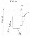
- Fig. 1 is an illustration for describing the outline of the principle of photodetection in an embodiment of the present disclosure.
- Fig. 1 schematically shows an element 90 including two electrodes 91 and 92 and a dielectric structure 94 sandwiched between them.
- Fig. 1 schematically shows the state in which a DC power source is connected to the electrodes 91 and 92 and an electric field is thereby applied from the outside to the dielectric structure 94.
- polarization occurs in the dielectric structure 94.
- An arrow P in Fig. 1 represents dielectric polarization in the dielectric structure 94.
- An arrow D represents electric flux density.
- ⁇ f is the density of electric charges in the electrodes
- ⁇ p is the density of electric charges generated by polarization within the dielectric structure 94 at its surfaces facing the electrodes.
- the dielectric structure 94 used is a structure including a photoelectric conversion layer. Therefore, when light enters the dielectric structure 94, hole-electron pairs are generated in the photoelectric conversion layer.
- a prescribed voltage is supplied between the electrodes 91 and 92 disposed so as to face each other with the dielectric structure 94 interposed therebetween, an electric field directed from the electrode 91 toward the electrode 92 is formed in the photoelectric conversion layer in the dielectric structure 94. This causes the holes and electrons formed in the photoelectric conversion layer by photoelectric conversion to be separated from each other. Part of the holes move toward the electrode 92, and part of the electrons move toward the electrode 91.
- the electric charges generated by photoelectric conversion are not extracted from the dielectric structure 94 to the outside through the electrode 91 or the electrode 92.
- the holes and electrons generated by photoelectric conversion are separated from each other, and the separated state is maintained.
- the separated charges cause the charge density ⁇ p to increase effectively.
- the permittivity of the dielectric structure 94 increases, as described above. This means that, when light enters the dielectric structure 94, the permittivity between the electrodes 91 and 92 changes.
- the capacitance value between the electrode 91 and the electrode 92 is changed. By detecting the change in the capacitance value, the light entering the dielectric structure 94 can be detected.
- Photosensors in the embodiments described below each have a structure capable of detecting light on the basis of a change in permittivity between two electrodes. It should be noted that, in the embodiments of the present disclosure, no electric charges are exchanged between the photoelectric conversion layer and the electrodes. Specifically, the electric charges generated in the photoelectric conversion layer by irradiation with light are retained within the photoelectric conversion layer and are basically not transferred to the electrodes. Basically, no electric charges are supplied from the electrodes to the photoelectric conversion layer. This is one of the differences from conventional solar cells and light emitting diodes utilizing photoelectric conversion.
- Fig. 2 shows the outline of an exemplary structure of a photosensor according to a first embodiment of the present disclosure.
- the photosensor 100A shown in Fig. 2 includes a photodetection element 10A and a voltage supply circuit 12 connected to the photodetection element 10A.
- the photodetection element 10A includes a first electrode 21, a second electrode 22, and a dielectric structure 2A disposed therebetween and including a photoelectric conversion layer 23A.
- Fig. 2 shows only schematically the arrangement of the components forming the photodetection element 10A, and the dimensions of the components shown in Fig. 2 do not strictly reflect the dimensions of an actual device. The same also applies to other figures in the present disclosure.
- a semiconductor material is used as the material forming the photoelectric conversion layer 23A.
- the photoelectric conversion layer 23A electron-hole pairs are generated in response to irradiation with light.
- an organic semiconductor material is used as the material forming the photoelectric conversion layer 23A. The details of the photoelectric conversion layer 23A will be described later.
- the voltage supply circuit 12 is configured such that prescribed voltages can be applied to the first electrode 21 and the second electrode 22. During photodetection, the voltage supply circuit 12 supplies a first voltage to the first electrode 21 and supplies a second voltage higher than the first voltage to the second electrode 22.
- the voltage supply circuit 12 is not limited to a specific power source circuit but may be a circuit generating the prescribed voltages or may be a circuit that converts a voltage supplied from another power source to the prescribed voltages.
- the first voltage and/or the second voltage may be applied in the form of pulses, or the application of the first voltage and/or the second voltage may be repeated periodically or quasi-periodically.
- At least one of the first electrode 21 and the second electrode 22 is a transparent electrode.
- the photoelectric conversion layer 23A receives light passing through the second electrode 22.
- the first electrode 21 to which the lower voltage is applied during photodetection may be a transparent electrode, or both the first electrode 21 and the second electrode 22 may be transparent electrodes.
- the term "transparent” as used herein means that at least part of light in a detection wavelength range is allowed to pass through, and it is not necessary that light in the entire visible wavelength range be allowed to pass through.
- the light detected by the photosensor of the present disclosure is not limited to light in the visible wavelength range (e.g., of from 380 nm to 780 nm inclusive).
- general electromagnetic waves including infrared rays and ultraviolet rays are expressed as "light" for convenience.
- the dielectric structure 2A includes a hole blocking layer 20h disposed between the first electrode 21 and the photoelectric conversion layer 23A.
- the dielectric structure 2A further includes an electron blocking layer 20e disposed between the second electrode 22 and the photoelectric conversion layer 23A.
- the hole blocking layer 20h and the electron blocking layer 20e have the function of retaining, within the photoelectric conversion layer 23A, electric charges generated in the photoelectric conversion layer 23A by photoelectric conversion.
- the hole blocking layer 20h has the function of suppressing movement of the holes generated by photoelectric conversion to the first electrode 21.
- the electron blocking layer 20e has the function of suppressing movement of the electrons generated by photoelectric conversion to the second electrode 22.
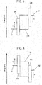
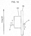
- Fig. 3 is an exemplary energy diagram of the photodetection element 10A.
- a thick horizontal line on the left of three rectangles represents the Fermi level of the first electrode 21, and a thick horizontal line on the right of the three rectangles represents the Fermi level of the second electrode 22.
- the base of the leftmost one of the three rectangles represents the energy level of the highest occupied molecular orbital (HOMO) of the hole blocking layer 20h, and its side opposed to the base represents the energy level of the lowest unoccupied molecular orbital (LUMO).
- the central and right rectangles in Fig. 3 schematically represent the HOMO and LUMO energy levels of the photoelectric conversion layer 23A and the electron blocking layer 20e, respectively. The same applies to other energy diagrams, unless otherwise specified.
- the first voltage is supplied from the voltage supply circuit 12 (not shown in Fig. 3 , see Fig. 2 ) to the first electrode 21, and the second voltage higher than the first voltage is applied to the second electrode 22.
- the second voltage higher than the first voltage is applied to the second electrode 22.
- an electric field directed from the right to the left in Fig. 3 is applied to the photoelectric conversion layer 23A from the outside.
- Thin arrows in the energy diagram shown in Fig. 3 schematically indicate the directions of the voltages applied to the first electrode 21 and the second electrode 22.
- the electron blocking layer 20e is disposed between the photoelectric conversion layer 23A and the second electrode 22, movement of electrons from the photoelectric conversion layer 23A to the second electrode 22 is blocked by an energy barrier between the photoelectric conversion layer 23A and the electron blocking layer 20e. Similarly, movement of holes from the photoelectric conversion layer 23A to the first electrode 21 is blocked by an energy barrier between the photoelectric conversion layer 23A and the hole blocking layer 20h. Specifically, movement of the electric charges generated by photoelectric conversion to the electrodes is suppressed, and the electric charges generated are retained within the photoelectric conversion layer 23A. As described above, in this embodiment of the present disclosure, the movement of the electric charges generated by photoelectric conversion to the electrodes is suppressed.
- the difference between the HOMO energy level of the photoelectric conversion layer 23A and the HOMO energy level of the hole blocking layer 20h is relatively large. Therefore, a relatively large potential barrier for holes is formed between the photoelectric conversion layer 23A and the hole blocking layer 20h. In this case, almost no holes move from the photoelectric conversion layer 23A to the hole blocking layer 20h.
- the HOMO energy level of the hole blocking layer 20h is deeper by desirably at least 0.3 eV and more desirably at least 0.7 eV than the HOMO energy level of the photoelectric conversion layer 23A.
- the difference between the LUMO energy level of the electron blocking layer 20e and the LUMO energy level of the photoelectric conversion layer 23A is relatively large, and therefore a relatively large potential barrier for electrons is formed between the electron blocking layer 20e and the photoelectric conversion layer 23A. In this case, almost no electrons move from the photoelectric conversion layer 23A to the electron blocking layer 20e.
- the LUMO energy level of the electron blocking layer 20e is shallower than the LUMO energy level of the photoelectric conversion layer 23A by desirably at least 0.3 eV and more desirably at least 0.7 eV.
- the hole blocking layer, the electron blocking layer, and the photoelectric conversion layer are formed of organic materials.
- these layers are formed of inorganic compounds, their HOMO is replaced with a valence band, and their LUMO is replaced with a conduction band.
- the difference between the Fermi level of the first electrode 21 and the LUMO energy level of the hole blocking layer 20h is relatively large. Therefore, a relatively high potential barrier for electrons is formed between the first electrode 21 and the hole blocking layer 20h. In this case, almost no electrons are injected from the first electrode 21 into the hole blocking layer 20h.
- the LUMO energy level of the hole blocking layer 20h is shallower than the Fermi level of the first electrode 21 by desirably at least 0.3 eV and more desirably at least 0.7 eV.
- the difference between the HOMO energy level of the electron blocking layer 20e and the Fermi level of the second electrode 22 is relatively large.
- a relatively high potential barrier for holes is formed between the electron blocking layer 20e and the second electrode 22. In this case, almost no holes are injected from the second electrode 22 into the electron blocking layer 20e.
- the HOMO energy level of the electron blocking layer 20e is deeper than the Fermi level of the second electrode 22 by desirably at least 0.3 eV and more desirably at least 0.7 eV.
- the hole blocking layer, the electron blocking layer, and the photoelectric conversion layer are formed of organic materials.
- these layers are formed of inorganic materials, their HOMO is replaced with a valence band, and their LUMO is replaced with a conduction band.
- the current density between the first electrode 21 and the second electrode 22 one second after the application of the voltage between the first electrode 21 and the second electrode 22 can be 1 ⁇ 10 -9 A/cm 2 or less.
- the electric charges generated by photoelectric conversion can be utilized as electric charges contributing to the change in the permittivity between the two electrodes (the first electrode 21 and the second electrode 22 in this case).
- the photodetection element 10A exemplified above includes the photoelectric conversion layer 23A formed using an organic semiconductor material.
- a device utilizing photoelectric conversion by an organic thin film include an imaging element having an organic thin film and an organic thin film solar cell.
- Functional layers such as the hole blocking layer and electron blocking layer may be used in the above devices.
- the conventional structures differ from the structure in this embodiment of the present disclosure in that the conventional structures must be configured such that electric charges generated by photoelectric conversion can be extracted from the photoelectric conversion layer to the electrodes along an electric field.
- Fig. 4 is an exemplary energy diagram of an imaging element having an organic thin film and shown as a comparative example.
- a hole blocking layer 80h is disposed between a pixel electrode 82 and a photoelectric conversion layer 83
- an electron blocking layer 80e is disposed between the photoelectric conversion layer 83 and a transparent electrode 81 (e.g., an ITO electrode) disposed so as to face the pixel electrode 82.
- a transparent electrode 81 e.g., an ITO electrode
- a prescribed voltage is applied to the transparent electrode 81, and holes or electrons generated in the photoelectric conversion layer 83 are thereby collected as signal charges by the pixel electrode 82.
- the pixel electrode 82 collects, as signal charges, electrons generated in the photoelectric conversion layer 83 by photoelectric conversion.
- Al, TiN, Cu, Al, TaN, or ITO is used as the material of the pixel electrode 82.
- no hole blocking layer 80h is disposed between the photoelectric conversion layer 83 and the electrode to which a lower voltage is applied (the transparent electrode 81 in this case).
- no electron blocking layer 80e is disposed between the photoelectric conversion layer 83 and the electrode to which a higher voltage is applied (the pixel electrode 82 in this case).
- the hole blocking layer 80h is disposed between the photoelectric conversion layer 83 and the electrode whose potential is higher during operation (the pixel electrode 82 in this case).
- the electron blocking layer 80e is disposed between the photoelectric conversion layer 83 and the electrode whose potential is lower during operation (the transparent electrode 81 in this case).
- the arrangement of the hole blocking layer and the electron blocking layer relative to the photoelectric conversion layer is inverted from that in the photosensor according to this embodiment of the present disclosure.
- the hole blocking layer 80h is provided for the purpose of allowing the electrons generated by photoelectric conversion to selectively pass therethrough from the photoelectric conversion layer 83 to the pixel electrode 82 while injection of holes from the pixel electrode 82 is suppressed.
- the electron blocking layer 80e is provided for the purpose of allowing the holes generated by photoelectric conversion to selectively pass therethrough from the photoelectric conversion layer 83 to the transparent electrode 81 while injection of electrons from the transparent electrode 81 is suppressed.
- its hole blocking layer must have the function of allowing electrons to selectively pass through while holes are blocked, and its electron blocking layer must have the function of allowing holes to selectively pass through while electrons are blocked.
- the rate of discharge of electric charges from the photoelectric conversion layer 83 and the rate of inflow of electric charges into the photoelectric conversion layer 83 are low.
- no electric charges are exchanged between the photoelectric conversion layer 23A and the first electrode 21 and between the photoelectric conversion layer 23A and the second electrode 22.
- this embodiment of the present disclosure it is only necessary that the positive and negative charges generated by photoelectric conversion be separated from each other, and detection can be performed at relatively high speed. Therefore, this embodiment of the present disclosure is advantageously applied to an image sensor.
- the holes or electrons generated by photoelectric conversion are not extracted as signal charges, and the amount of the signal charges is not read, so that a so-called reset operation is unnecessary.
- the photosensor according to this embodiment of the present disclosure when the application of the electric field to the photoelectric conversion layer is stopped, the holes and the electrons are recombined, and the permittivity of the dielectric structure that has been increased by irradiation with light decreases.
- a reset operation performed by supplying a reset voltage is unnecessary, and this is advantageous to increase the speed of operation. It is unnecessary to provide a separate reset circuit, and this is advantageous for miniaturization.
- the configuration of the hole blocking layer 20h and the electron blocking layer 20e in the photodetection element is determined such that movement of electric charges from the photoelectric conversion layer 23A to the first electrode 21 and movement of electric charges from the photoelectric conversion layer 23A to the second electrode 22 can be suppressed.
- the materials of the first electrode 21, the hole blocking layer 20h, the photoelectric conversion layer 23A, the electron blocking layer 20e, and the second electrode 22 and the values of the first and second voltages are selected such that the relative relations among the energy levels of the components of the photodetection element 10A and the direction of the voltage applied between the first electrode 21 and the second electrode 22 are as shown in Fig. 3 .
- the movement of electric charges from the photoelectric conversion layer 23A to the first electrode 21 and the movement of electric charges from the photoelectric conversion layer 23A to the second electrode 22 are suppressed. Therefore, the electric charges generated when light enters the photoelectric conversion layer 23A through the first electrode 21 and/or the second electrode 22 are retained within the photoelectric conversion layer 23A. Since the electric charges generated by photoelectric conversion are retained within the photoelectric conversion layer 23A, the permittivity of the dielectric structure 2A including the photoelectric conversion layer 23A increases. Specifically, the capacitance value between the first electrode 21 and the second electrode 22 in the photosensor 100A changes when light enters the photosensor 100A.
- the photosensor 100A By detecting the change in the capacitance value between the first electrode 21 and the second electrode 22 as a change in electric current or voltage using an appropriate detection circuit, the light entering the photosensor 100A can be detected. As described above, the photosensor 100A can generate a signal corresponding to the change in the permittivity of the dielectric structure 2A caused by the incident light.
- the first voltage and/or second voltage is not necessarily a steady constant voltage and may be a voltage varying with time.
- the second voltage used is higher than the first voltage.
- the second voltage is not limited to a voltage that is always higher than the first voltage. When the voltages vary with time, the second voltage may be equal to the first voltage in some instances.
- One of the hole blocking layer 20h and the electron blocking layer 20e can be omitted by selecting an appropriate combination of the materials of the first electrode 21, the photoelectric conversion layer 23A, and the second electrode 22 in consideration of the magnitude of the ionization potential or electron affinity of the photoelectric conversion layer 23A and the magnitudes of the work functions of the electrodes (the first electrode 21 and the second electrode 22). Examples of such a structure will be described later.
- the work function of an electrode is defined as the difference between the vacuum level and the Fermi level of the electrode.
- the ionization potential is defined as the difference between the vacuum level and the HOMO
- the electron affinity is defined as the difference between the vacuum level and the LUMO.
- WF work function
- IP IP
- EA electron affinity
- the photoelectric conversion layer 23A contains, for example, tin naphthalocyanine represented by general formula (1) below (hereinafter may be referred to simply as "tin naphthalocyanine").
- R 1 to R 24 each independently represent a hydrogen atom or a substituent.
- the substituent is not limited to a specific substituent.
- the substituent may be selected from a deuterium atom, halogen atoms, alkyl groups (including cycloalkyl groups, bicycloalkyl groups, and tricycloalkyl groups), alkenyl groups (including cycloalkenyl groups and bicycloalkenyl groups), alkynyl groups, aryl groups, heterocyclic groups, a cyano group, a hydroxy group, a nitro group, a carboxy group, alkoxy groups, aryloxy groups, silyloxy groups, heterocyclic oxy groups, acyloxy groups, a carbamoyloxy group, alkoxycarbonyloxy groups, aryloxycarbonyloxy groups, amino groups (including an anilino group), an ammonio group, acylamino groups, an aminocarbonylamino group, alkoxycarbonyla
- a commercial product may be used as the tin naphthalocyanine represented by general formula (1) above.
- the tin naphthalocyanine represented by general formula (1) above can be synthesized using a naphthalene derivative represented by general formula (2) below as a starting material.
- R 25 to R 30 in general formula (2) may be selected from the same substituents as those for R 1 to R 24 in general formula (1).
- tin naphthalocyanine represented by general formula (1) above it is beneficial, in terms of ease of controlling the cohesion state of the molecules, that at least eight of R 1 to R 24 are each a hydrogen atom or a deuterium atom. It is more beneficial that at least sixteen of R 1 to R 24 are each a hydrogen atom or a deuterium atom, and it is still more beneficial that all of R 1 to R 24 are each a hydrogen atom or a deuterium atom.
- Tin naphthalocyanine represented by formula (3) below is advantageous in terms of ease of synthesis.
- the tin naphthalocyanine represented by general formula (1) above exhibits absorption in the wavelength range of from about 200 nm to 1,100 nm inclusive.
- the absorption peak of tin naphthalocyanine can be located at a wavelength of about 940 nm.
- the tin naphthalocyanine represented by formula (3) above has an absorption peak at a wavelength of about 870 nm as shown in Fig. 5.
- Fig. 5 is an example of the absorption spectrum in a photoelectric conversion layer containing the tin naphthalocyanine represented by formula (3) above.
- the quantum efficiency of the photoelectric conversion layer containing the tin naphthalocyanine represented by formula (3) at a wavelength of 900 nm can be about 10 times higher than that of silicon.
- a sample in which the photoelectric conversion layer (thickness: 30 nm) was stacked on a quartz substrate was used.
- the photoelectric conversion layer formed from a material containing the tin naphthalocyanine exhibits absorption in the near infrared region.
- the material containing the tin naphthalocyanine as the material forming the photoelectric conversion layer 23A, a photosensor capable of detecting near infrared rays can be obtained.
- a photosensor having sensitivity in the desired wavelength range can be obtained.
- P3HT poly(3-hexylthiophene-2,5-diyl)
- P3HT poly(3-hexylthiophene-2,5-diyl)
- copper phthalocyanine has absorption peaks at wavelengths of 620 nm and 700 nm.
- the photoelectric conversion layer 23A may be formed from an organic p-type semiconductor (compound) described later or may be formed from an organic n-type semiconductor (compound) described later. Alternatively, a combination of an organic p-type semiconductor (compound) and an organic n-type semiconductor (compound) may be used to form the photoelectric conversion layer 23A.
- the photoelectric conversion layer 23A may contain an inorganic semiconductor material such as amorphous silicon.
- the photoelectric conversion layer 23A may include a layer formed from an organic material and a layer formed from an inorganic material.
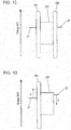
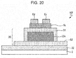
- FIG. 6 shows an example of the structure of a photodetection element including a photoelectric conversion layer formed using an organic semiconductor material containing the tin naphthalocyanine represented by general formula (1) above.
- a dielectric structure 2B in the photodetection element 10B shown in Fig. 6 includes a hole blocking layer 20h, a photoelectric conversion layer 23B, and an electron blocking layer 20e.
- the hole blocking layer 20h is disposed between a first electrode 21 and the photoelectric conversion layer 23B
- the electron blocking layer 20e is disposed between the photoelectric conversion layer 23B and a second electrode 22.
- the photoelectric conversion layer 23B contains at least one of a p-type semiconductor and an n-type semiconductor.
- the photoelectric conversion layer 23B includes a p-type semiconductor layer 230p, an n-type semiconductor layer 230n, and a mixed layer 230h sandwiched between the p-type semiconductor layer 230p and the n-type semiconductor layer 230n.
- the p-type semiconductor layer 230p is disposed between the hole blocking layer 20h and the mixed layer 230h and functions as a photoelectric conversion layer and/or a hole transport layer.
- the n-type semiconductor layer 230n is disposed between the mixed layer 230h and the electron blocking layer 20e and functions as a photoelectric conversion layer and/or an electron transport layer. As described later, the mixed layer 230h contains a p-type semiconductor and an n-type semiconductor.
- the p-type semiconductor layer 230p and the n-type semiconductor layer 230n contain an organic p-type semiconductor and an organic n-type semiconductor, respectively.
- the photoelectric conversion layer 23B may contain an organic photoelectric conversion material containing the tin naphthalocyanine represented by general formula (1) above and at least one of an organic p-type semiconductor and an organic n-type semiconductor.
- the organic p-type semiconductor is a donating organic semiconductor (compound) typified mainly by a hole transport organic compound and is an organic compound having the property of easily donating electrons. More specifically, when two organic materials in contact with each other are used, one of the organic materials that has a lower ionization potential is an organic p-type semiconductor (compound). Therefore, any organic compound having the ability to donate electrons can be used as the donating organic compound.
- organic compound examples include triarylamine compounds, benzidine compounds, pyrazoline compounds, styrylamine compounds, hydrazone compounds, triphenylmethane compounds, carbazole compounds, polysilane compounds, thiophene compounds such as P3HT, phthalocyanine compounds such as copper phthalocyanine, cyanine compounds, merocyanine compounds, oxonol compounds, polyamine compounds, indole compounds, pyrrole compounds, pyrazole compounds, polyarylene compounds, condensed aromatic carbocyclic compounds (naphthalene derivatives, anthracene derivatives, phenanthrene derivatives, tetracene derivatives, pyrene derivatives, perylene derivatives, and fluoranthene derivatives), and metal complexes containing a nitrogen-containing heterocyclic compound as a ligand.
- phthalocyanine compounds such as copper phthalocyanine, cyanine compounds, merocyanine compounds, oxonol compounds
- the donating organic semiconductor is not limited to these compounds, and any other organic compound that has a lower ionization potential than an organic compound used as the n-type (accepting) compound can be used as the donating organic semiconductor, as described above.
- the tin naphthalocyanine described above is an example of the organic p-type semiconductor material.
- the organic n-type semiconductor is an accepting organic semiconductor (compound) typified mainly by an electron transport organic compound and is an organic compound having the property of easily accepting electrons. More specifically, when two organic materials in contact with each other are used, one of the organic materials that has a higher electron affinity is an organic n-type semiconductor (compound). Therefore, any organic compound having the ability to accept electrons can be used as the accepting organic compound.
- organic compound examples include fullerenes, fullerene derivatives such as phenyl-C 61 -butyric acid methyl ester (PCBM), condensed aromatic carbocyclic compounds (naphthalene derivatives, anthracene derivatives, phenanthrene derivatives, tetracene derivatives, pyrene derivatives, perylene derivatives, and fluoranthene derivatives), 5- to 7-membered nitrogen, oxygen, and/or sulfur atom-containing heterocyclic compounds (such as pyridine, pyrazine, pyrimidine, pyridazine, triazine, quinoline, quinoxaline, quinazoline, phthalazine, cinnoline, isoquinoline, pteridine, acridine, phenazine, phenanthroline, tetrazole, pyrazole, imidazole, thiazole, oxazole, indazole, benz
- the dielectric structure 2B has the photoelectric conversion layer 23B including the p-type semiconductor layer 230p and the n-type semiconductor layer 230n as exemplified in Fig. 6 , holes and electrons generated by photoelectric conversion can be easily separated from each other. Therefore, when the photoelectric conversion layer 23B including the p-type semiconductor layer 230p and the n-type semiconductor layer 230n is used, the efficiency of charge separation is improved, and a change in the intensity of incident light can cause a larger change in permittivity.
- the mixed layer 230h may be, for example, a bulk heterojunction structure layer containing a p-type semiconductor and an n-type semiconductor.
- the tin naphthalocyanine represented by general formula (1) above may be used as the p-type semiconductor material.
- the n-type semiconductor material used may be a fullerene and/or a fullerene derivative.
- the details of the bulk heterojunction structure are described in Japanese Patent No. 5553727 . The entire disclosure of Japanese Patent No. 5553727 is incorporated herein for reference purposes.
- the material used to form the hole blocking layer 20h may be an n-type semiconductor or an electron transport organic compound.
- examples of such materials include: organic materials and organic-metal compounds such as fullerenes, e.g., C 60 and C 70 , fullerene derivatives, e.g., indene-C 60 bisadduct (ICBA), carbon nanotubes and derivatives thereof, oxadiazole derivatives, e.g., OXD-7 (1,3-bis(4-tert-butylphenyl-1,3,4-oxadiazolyl)phenylene), anthraquinodimethane derivatives, diphenylquinone derivatives, bathocuproine (BCP), bathophenanthroline and derivatives thereof, distyrylarylene derivatives, triazole compounds, silole compounds, a tris(8-hydroxyquinolinato)aluminum complex, a bis(4-methyl-8-quinolinato)aluminum complex, acety
- the hole blocking layer 20h may be reduced in thickness.
- the hole blocking layer 20h may have a thickness within the range of, for example, from 5 nm to 50 nm inclusive.
- the material used to form the electron blocking layer 20e may be a p-type semiconductor or a hole transport organic compound.
- aromatic diamine compounds such as TPD (N,N'-bis(3-methylphenyl)-(1,1'-biphenyl)-4,4'-diamine) and ⁇ -NPD (4,4'-bis[N-(naphthyl)-N-phenyl-amino]biphenyl), oxazole, oxadiazole, triazole, imidazole, imidazolone, stilbene derivatives, pyrazoline derivatives, tetrahydroimidazole, polyarylalkanes, butadiene, m-MTDATA (4,4',4"-tris(N-(3-methylphenyl)N-phenylamino)triphenylamine), perylene, porphyrin compounds such as porphine, copper tetraphenylporphine, phthalocyanine,
- the material used to form the electron blocking layer 20e may be: polymers of phenylenevinylene, fluorene, carbazole, indole, pyrene, pyrrole, picoline, thiophene, acetylene, and diacetylene; and derivatives thereof.
- the material used to form the electron blocking layer 20e is selected from the above materials in consideration of the electron affinity of the photoelectric conversion layer 23A (or the n-type semiconductor layer 230n in the photoelectric conversion layer 23B).
- the electron blocking layer 20e may be reduced in thickness.
- the electron blocking layer 20e may have a thickness within the range of, for example, from 5 nm to 50 nm inclusive.
- the photoelectric conversion layer (the photoelectric conversion layer 23A or 23B), and the second electrode 22
- one of the hole blocking layer 20h and the electron blocking layer 20e can be omitted. Examples of such a structure will next be described.
- Fig. 7 is an exemplary energy diagram of a photodetection element in which the hole blocking layer 20h and a photoelectric conversion layer 23C are disposed between the first electrode 21 and the second electrode 22.
- the photoelectric conversion layer 23C is adjacent to the second electrode 22 to which the second voltage is applied.
- Fig. 7 shows a structural example in which the electron blocking layer 20e is omitted.
- the photoelectric conversion layer 23C has a heterojunction structure between the p-type semiconductor layer 230p and the n-type semiconductor layer 230n.
- the photoelectric conversion layer 23C may have a bulk heterojunction structure.
- the hole blocking layer 20h suppresses movement of holes from the photoelectric conversion layer 23C to the first electrode 21.
- the difference between the LUMO of the hole blocking layer 20h and the Fermi level of the first electrode 21 is large, and therefore a potential barrier for electrons is formed between the first electrode 21 and the hole blocking layer 20h.
- the potential barrier suppresses movement of electrons from the first electrode 21 to the hole blocking layer 20h. In other words, transport of electrons from the first electrode 21 to the hole blocking layer 20h is suppressed without using an electron blocking layer.
- the photoelectric conversion layer (the photoelectric conversion layer 23C in this case) and an electrode (the second electrode 22 in this case) are disposed adjacent to each other
- the ionization potential of the photoelectric conversion layer 23C is higher than the work function of the second electrode 22, and the difference between the HOMO of the photoelectric conversion layer 23C and the Fermi level of the second electrode 22 is relatively large. Therefore, the potential barrier between the photoelectric conversion layer 23C and the second electrode 22 suppresses injection of holes from the second electrode 22 into the photoelectric conversion layer 23C.
- the charges generated by photoelectric conversion can be retained within the photoelectric conversion layer 23C.
- the permittivity can be changed in response to irradiation with light when the materials of the first electrode 21, the hole blocking layer 20h, the photoelectric conversion layer 23C, and the second electrode 22 are appropriately selected such that the relative relations among the energies of the components of the photodetection element are as shown in Fig. 7 .
- Fig. 8 schematically shows the relative relations among the energies obtained by the above combination.
- an arrow ⁇ 1 represents a potential barrier for electrons between the hole blocking layer 20h and the first electrode 21
- an arrow ⁇ 2 represents a potential barrier for holes between the n-type semiconductor layer 230n and the second electrode 22.
- An arrow ⁇ 3 represents a potential barrier for holes between the p-type semiconductor layer 230p and the hole blocking layer 20h.
- the above combination is merely an example.
- P3HT, tin naphthalocyanine, etc. may be used instead of copper phthalocyanine exemplified as the material of the p-type semiconductor layer 230p.
- Fig. 9 is an exemplary energy diagram of a photodetection element in which the photoelectric conversion layer 23C and the electron blocking layer 20e are disposed between the first electrode 21 and the second electrode 22. As illustrated, in this example, the photoelectric conversion layer 23C is adjacent to the first electrode 21 to which the first voltage is applied. Specifically, Fig. 9 shows a structural example in which the hole blocking layer 20h is omitted.
- the electron blocking layer 20e suppresses movement of electrons from the photoelectric conversion layer 23C to the second electrode 22.
- the difference between the HOMO of the electron blocking layer 20e and the Fermi level of the second electrode 22 is large, and a potential barrier for holes is formed between the electron blocking layer 20e and the second electrode 22.
- This potential barrier suppresses movement of holes from the second electrode 22 to the electron blocking layer 20e. In other words, transport of holes from the second electrode 22 to the electron blocking layer 20e is suppressed without using a hole blocking layer.
- the photoelectric conversion layer (the photoelectric conversion layer 23C in this case) and an electrode (the first electrode 21 in this case) are disposed adjacent to each other
- the electron affinity of the photoelectric conversion layer 23C is lower than the work function of the first electrode 21, and the difference between the Fermi level of the first electrode 21 and the LUMO of the photoelectric conversion layer 23C is relatively large. Therefore, a potential barrier is formed between the first electrode 21 and the photoelectric conversion layer 23C.
- This potential barrier suppresses injection of electrons from the first electrode 21 into the photoelectric conversion layer 23C.
- the permittivity can be changed in response to irradiation with light when the materials of the first electrode 21, the photoelectric conversion layer 23C, the electron blocking layer 20e, and the second electrode 22 are appropriately selected such that the relative relations among the energies of the components of the photodetection element are as shown in Fig. 9 .
- One example of the combination of the materials of the first electrode 21, the photoelectric conversion layer 23C, the electron blocking layer 20e, and the second electrode 22 that are combined so as to satisfy the relative relations among the energies of the components of the photodetection element in Fig. 9 is as follows.
- FIG. 10 schematically shows the relative relations among the energies obtained by the above combination.
- an arrow ⁇ 5 represents a potential barrier for electrons between the first electrode 21 and the p-type semiconductor layer 230p.
- An arrow ⁇ 6 represents a potential barrier for holes between the electron blocking layer 20e and the second electrode 22, and an arrow ⁇ 7 represents a potential barrier for electrons between the n-type semiconductor layer 230n and the electron blocking layer 20e.
- P3HT, tin naphthalocyanine, etc. may be used instead of copper phthalocyanine exemplified below. Copper phthalocyanine may be used instead of perylene exemplified as the material of the electron blocking layer 20e.
- the photodetection element in which the hole blocking layer 20h or the electron blocking layer 20e is omitted can also suppress movement of electric charges generated by photoelectric conversion to the electrodes.
- the same effects as those of the photodetection element having both the hole blocking layer 20h and the electron blocking layer 20e can be obtained using the simpler structures.
- the position of the interposed blocking layer is determined according to which of the two electrodes is at a higher electric potential under the application of voltage.
- an insulating layer that does not allow holes and electron to pass through may be used instead of the hole blocking layer 20h and/or the electron blocking layer 20e.
- a description will be given of an example of the structure in which an insulating layer is disposed between a photoelectric conversion layer and electrodes.
- Fig. 11 shows the outline of an exemplary structure of a photosensor according to a second embodiment of the present disclosure.
- the photosensor 100C shown in Fig. 11 includes: a photodetection element 10C including a dielectric structure 2C disposed between a first electrode 21 and a second electrode 22; and a voltage supply circuit 12.
- the dielectric structure 2C includes an insulating layer 29a and an insulating layer 29b. As illustrated, the insulating layer 29a is disposed between the first electrode 21 and the photoelectric conversion layer 23C.
- the insulating layer 29b is disposed between the photoelectric conversion layer 23C and the second electrode 22.
- Fig. 12 is an exemplary energy diagram of the photodetection element 10C.
- the base of the leftmost one of three rectangles represents the upper edge of the valence band of the insulating layer 29a, and the side opposite to the base represents the bottom of its conduction band.
- the rightmost rectangle in Fig. 12 schematically shows the energy levels of the upper edge of the valence band of the insulating layer 29b and the bottom of its conduction band.
- the difference between the upper edge of a valence band and the vacuum level and the difference between the bottom of a conduction band and the vacuum level may be represented by VB and CB, respectively.
- the insulating layer 29a between the first electrode 21 and the photoelectric conversion layer 23C, movement of electric charges between the first electrode 21 and the photoelectric conversion layer 23C can be suppressed even when a voltage is applied between the first electrode 21 and the second electrode 22.
- the insulating layer 29b between the second electrode 22 and the photoelectric conversion layer 23C, movement of electric charges between the second electrode 22 and the photoelectric conversion layer 23C can be suppressed. Therefore, the electric charges generated by photoelectric conversion are suppressed from migrating to the electrodes (the first electrode 21 and/or the second electrode 22) and can be used as electric charges contributing to a change in the permittivity of the dielectric structure 2C.
- the “insulating layers” as used herein are distinguished from the hole blocking layer 20h and the electron blocking layer 20e because the insulating layers block the movement of both the positive and negative charges irrespective of the direction of the electric field applied from the outside.
- the “insulating layers” as used herein suppress both the positive and negative charges from migrating from the electrodes to the photoelectric conversion layer and from migrating from the photoelectric conversion layer to the electrodes.
- the material used to form the insulating layers 29a and 29b may be, for example, an oxide such as SiO 2 , Al 2 O 3 , ZrO 2 , HfO 2 , or Y 2 O 3 or a resin such as polymethyl methacrylate (PMMA), polyimide, parylene (registered trademark), or polystyrene.
- PMMA polymethyl methacrylate
- PMMA polymethyl methacrylate
- polyimide polyimide
- parylene registered trademark
- polystyrene polystyrene.
- a silicon oxynitride film (SiON film) generally used for silicon semiconductors may be used for the insulating layer 29a and/or the insulating layer 29b.
- a so-called high-permittivity material (referred to also as a high-k material and having a relative permittivity of typically more than 3.9) is used to form the insulating layer 29a and/or the insulating layer 29b.
- the thicknesses of the insulating layer 29a and the insulating layer 29b may be appropriately set according to the electric conductivities of the insulating layer 29a and the insulating layer 29b.
- the insulating layer 29a is disposed between the first electrode 21 and the photoelectric conversion layer 23C. Moreover, the insulating layer 29b is disposed between the photoelectric conversion layer 23C and the second electrode 22. Therefore, during operation of the photosensor 100C, any one of the first electrode 21 and the second electrode 22 may be at a higher potential than the other. Specifically, the structure exemplified in Fig. 11 has an advantage in that less restrictions are imposed on the material of the first electrode 21 and the material of the second electrode 22.
- the material used for the second electrode 22 may be a transparent conductive oxide (TCO) such as ITO, IZO, AZO, FTO, SnO 2 , TiO 2 , or ZnO 2 , a carbon nanotube, graphene, etc.
- TCO transparent conductive oxide
- the material used for the second electrode 22 may be Al, TiN, Cu, TaN, etc.
- the material used for the first electrode 21 may be selected from the same materials as those for the second electrode 22.
- the material used for the first electrode 21 may be Al, TiN, Cu, TaN, ITO, etc.
- one of the insulating layers 29a and 29b can be omitted by selecting an appropriate combination of the materials of the first electrode 21, the photoelectric conversion layer 23C (or the photoelectric conversion layer 23A or 23B), and the second electrode 22.
- Fig. 13 is an exemplary energy diagram of a photodetection element in which the insulating layer 29a and the photoelectric conversion layer 23C are disposed between the first electrode 21 and the second electrode 22. As illustrated, in this example, the photoelectric conversion layer 23C is adjacent to the second electrode 22 to which the second voltage is applied. Specifically, Fig. 13 shows a structural example in which the insulating layer 29b is omitted.
- the insulating layer 29a suppresses movement of holes from the photoelectric conversion layer 23C to the first electrode 21 and movement of electrons from the first electrode 21 to the photoelectric conversion layer 23C.
- the ionization potential of the photoelectric conversion layer 23C is set to be larger than the work function of the second electrode 22. Therefore, injection of holes from the second electrode 22 into the photoelectric conversion layer 23C is suppressed by the potential barrier between the photoelectric conversion layer 23C and the second electrode 22.
- part of electric charges (e.g., holes) generated by photoelectric conversion can be retained within the photoelectric conversion layer 23C and can be utilized as electric charges contributing to a change in the permittivity of the photoelectric conversion layer 23C.
- the insulating layer 29b is not provided between the photoelectric conversion layer 23C and the second electrode 22, movement of electric charges generated by photoelectric conversion to the electrodes can be suppressed by appropriately selecting the materials of the first electrode 21, the insulating layer 29a, the photoelectric conversion layer 23C, and the second electrode 22 such that the relative relations among the energies of the components of the photodetection element are as shown in Fig. 13 .
- Fig. 14 schematically shows the relative relations among the energies obtained by the above combination.
- the material used for the second electrode 22 may be a metal having a work function of from about 4.1 eV to about 4.3 eV inclusive. Therefore, instead of Al exemplified below, Ti, Ta, Ag, etc. may be used.
- the material used for the n-type semiconductor layer 230n adjacent to the second electrode 22 may be a material having an ionization potential of about 5 eV or more.
- Al 2 O 3 exemplified as the material of the insulating layer 29a, SiO 2 , ZrO 2 , HfO 2 , Y 2 O 3 , etc. may be used.
- Fig. 15 is an exemplary energy diagram of a photodetection element in which the photoelectric conversion layer 23C and the insulating layer 29b are disposed between the first electrode 21 and the second electrode 22. As illustrated, in this example, the photoelectric conversion layer 23C is adjacent to the first electrode 21 to which the first voltage is applied. Specifically, Fig. 15 shows an example in which the insulating layer 29a is omitted.
- the insulating layer 29b blocks movement of electrons from the photoelectric conversion layer 23C to the second electrode 22 and movement of holes from the second electrode 22 to the photoelectric conversion layer 23C.
- the electron affinity of the photoelectric conversion layer 23C is set to be lower than the work function of the first electrode 21. In this case, injection of electrons from the first electrode 21 into the photoelectric conversion layer 23C is suppressed by the potential barrier between the first electrode 21 and the photoelectric conversion layer 23C.
- part of electric charges (e.g., electrons) generated by photoelectric conversion can be retained within the photoelectric conversion layer 23C and can be used as electric charges contributing to a change in the permittivity of the photoelectric conversion layer 23C.
- the insulating layer 29a is not provided between the first electrode 21 and the photoelectric conversion layer 23C, movement of electric charges generated by photoelectric conversion to the electrodes can be suppressed by appropriately selecting the materials of the first electrode 21, the photoelectric conversion layer 23C, the insulating layer 29b, and the second electrode 22 such that the relative relations among the energies of the components of the photodetection element are as shown in Fig. 15 .
- Fig. 16 schematically shows the relative relations among the energies obtained by the above combination.
- the material used for the first electrode 21 may be a metal having a work function of about 4.8 eV or more.
- Pt, Ni, ITO, etc. may be used instead of Au exemplified below.
- Fig. 17 schematically shows the structure of a photodetection element used for measurement of the change in permittivity.
- the photodetection element 10D having the structure shown in Fig. 17 was produced using the following procedure.
- a glass substrate 2GL was prepared.
- ITO was deposited on the glass substrate 2GL by sputtering to thereby form an ITO electrode (thickness: 50 nm) serving as a second electrode 22.
- atomic layer deposition ALD was used to form a HfO 2 layer (thickness: 30 nm) serving as an insulating layer 29b on the second electrode 22.
- tin naphthalocyanine and C 60 were co-evaporated to form a co-evaporated layer (thickness: 150 nm) serving as a photoelectric conversion layer 23D on the insulating layer 29b.
- ALD was used to form an Al 2 O 3 layer (thickness: 30 nm) serving as an insulating layer 29a on the photoelectric conversion layer 23D.
- sputtering was used to deposit Al on the insulating layer 29a to thereby form an Al electrode (thickness: 80 nm) serving as a first electrode 21.
- a photodetection element 10D having the structure shown in Fig. 17 was obtained.
- the shape of the photoelectric conversion layer 23D was a rectangle with 1 mm sides when viewed in a direction normal to the glass substrate 2GL.
- an LED light source (wavelength: 940 nm, rated power consumption: about 70 mW) was used.
- a measuring apparatus 300 was connected to the first electrode 21 and the second electrode 22 to apply a potential difference of 4 V between the first electrode 21 and the second electrode 22.
- the capacitance value of a dielectric structure 2D between the first electrode 21 and the second electrode 22 was measured.
- a semiconductor device parameter analyzer B1500A (measurement frequency: 1 kHz, amplitude: 0.1 V) manufactured by Keysight was used.
- a LOW side of a probe of the measuring apparatus was brought into contact with the first electrode 21, and a HIGH side of the probe was brought into contact with the second electrode 22.
- Fig. 18 shows the results of the measurement of the capacitance value of the dielectric structure 2D.
- open squares ( ⁇ ) show the results of the capacitance value measurement when the photoelectric conversion layer 23D was not irradiated with light (LED light source: off, dark condition).
- Open triangles ( ⁇ ) show the results of the capacitance value measurement when the photoelectric conversion layer 23D was irradiated with light (LED light source: on).
- the capacitance value without light irradiation was about 6.3 ⁇ F
- the capacitance value under light irradiation was about 2 ⁇ F. Therefore, in this example, when the photoelectric conversion layer 23D was irradiated with light, the capacitance value of the dielectric structure 2D was increased by a factor of about 3 as compared to that in the dark condition.
- a photosensor in which the capacitance value between its electrodes changes in response to a change in illuminance can be obtained.
- Fig. 19 shows an example of the device structure of the photodetection element.
- the photodetection element 10E shown in Fig. 19 is supported by a substrate 2.
- the substrate 2 used may be, for example, a silicon substrate having an oxide film on its surface, a glass substrate, or a polyimide substrate.
- a second electrode 22 is disposed on the substrate 2.
- a dielectric structure 2E disposed between a first electrode 21 and the second electrode 22 includes barrier layers B1 and B2 and a photoelectric conversion layer 23A.
- the barrier layer B1 disposed between the first electrode 21 and the photoelectric conversion layer 23A may be the hole blocking layer 20h described above or the insulating layer 29a described above.
- the barrier layer B1 is a layer having the function of suppressing at least transport of holes from the photoelectric conversion layer (the photoelectric conversion layer 23A in this case) to the first electrode 21.
- the barrier layer B2 disposed between the photoelectric conversion layer 23A and the second electrode 22 may be the electron blocking layer 20e described above or the insulating layer 29b described above.
- the barrier layer B2 is a layer having the function of suppressing at least transport of electrons from the photoelectric conversion layer (the photoelectric conversion layer 23A in this case) to the second electrode 22.
- light entering the photoelectric conversion layer 23A can be detected as a change in the capacitance value between the first electrode 21 and the second electrode 22.
- the light may enter from the first electrode 21 side or may enter from the second electrode 22 side.
- the first electrode 21 is a transparent electrode
- the light may enter the photoelectric conversion layer 23A through the first electrode 21.
- the substrate 2 is a transparent substrate and the second electrode 22 is a transparent electrode
- the light may enter the photoelectric conversion layer 23A through the substrate 2 and the second electrode 22.
- the voltage supply circuit 12 (see, for example, Fig. 2 ) is not illustrated and is omitted.
- the voltage supply circuit 12 may be disposed on the substrate.
- the change in the capacitance value between the first electrode 21 and the second electrode 22 may be detected, for example, in the following manner.
- the capacitance can be computed from the following formula.
- C p 1 ⁇ A 1 + D 2
- an appropriate one of the above two formulas can be selected according to the structure of the element and the frequency of the AC voltage.
- Fig. 22 schematically shows a cross section of a photodetector including the capacitor structure of the present disclosure.
- a photosensor 100C includes a transistor 60 and a photoelectric conversion unit.
- the transistor 60 is a field effect transistor formed on a semiconductor substrate 20.
- the transistor 60 includes an impurity region 20d, an impurity region 20s, an insulating layer 23x on the semiconductor substrate, and a gate electrode 24 on the insulating layer 23x.
- the impurity region 20d functions as a drain region (or a source region) of the transistor 60, and the impurity region 20s function as the source region (or the drain region) of the transistor 60.
- the impurity region 20d is connected to a power source line 42, so that a prescribed voltage can be applied to the impurity region 20d during operation of the photodetector 1000.
- the insulating layer 23x functions as a gate insulating layer of the transistor 60.
- the insulating layer 23x is, for example, a thermally oxidized silicon film having a thickness of 4.6 nm.
- the photoelectric conversion unit of the photosensor 100C includes a pixel electrode 21, a transparent electrode 22 facing the pixel electrode 21, and a photoelectric conversion layer 23p sandwiched therebetween.
- An insulating layer 29a is disposed between the pixel electrode 21 and the photoelectric conversion layer 23p, and an insulating layer 29b is disposed between the photoelectric conversion layer 23p and the transparent electrode 22.
- the pixel electrode 21 is disposed so as to be spaced apart from adjacent unit pixel cells 10C. Therefore, the pixel electrode 21 is electrically isolated from pixel electrodes 21 of other unit pixel cells 10C.
- the pixel electrode 21 is typically a metal electrode or a metal nitride electrode.
- Examples of the material for forming the pixel electrode 21 include Al, Cu, Ti, TiN, Ta, TaN, Mo, Ru, and Pt.
- the pixel electrode 21 may be formed from polysilicon doped with an impurity to impart electrical conductivity. In the above case, the pixel electrode 21 used is a TiN electrode.
- a material through which a smaller leakage current can flow than through the material forming the photoelectric conversion layer 23p may be selected as the material forming the insulating layers 29a and 29b.
- a silicon oxide film having a thickness of 5.4 nm is used for the insulating layers 29a and 29b.
- the silicon oxide film can be formed by, for example, CVD.
- the photoelectric conversion layer 23p is formed so as to extend over other unit pixel cells 10C.
- the thickness of the photoelectric conversion layer 23p may be, for example, about 200 nm.
- the transparent electrode 22 is formed using a transparent conducting oxide (TCO) so as to extend over other unit pixel cells 10C.
- TCO transparent conducting oxide
- the transparent electrode 22 is connected to a gate voltage control line (not illustrated), so that a prescribed voltage can be applied to the transparent electrode 22 during operation of the photodetector 1000.
- the transparent electrode 22 and the photoelectric conversion layer 23p are disposed above an interlayer insulating layer 50, and the pixel electrode 21 of the photoelectric conversion unit is connected to the gate electrode 24 of the capacitance-modulated transistor 60 through a connection portion 54 including part of multilayer wiring 40 and a contact plug 52.
- a first voltage applied to the impurity region 20d is 1.2 V
- a second voltage applied to the transparent electrode 22 is 3.7 V.
- a potential difference of about 2.5 V is applied between the impurity region 20d and the transparent electrode 22.
- Fig. 23 shows the film thickness dependence of a leakage current flowing through the silicon oxide film when a voltage of 2.5 V is applied.
- the leakage current to the channel region of the capacitance-modulated transistor 60 is 1 ⁇ 10 -11 A/cm 2 or less.
- the leakage current through the silicon oxide film can be reduced to 1 ⁇ 10 -11 A/cm 2 or less when the thickness of the silicon oxide film is 5.4 nm or more.
- the permittivity of the photoelectric conversion layer 23p changes.
- the permittivity of the photoelectric conversion layer 23p changes, the effective gate voltage of the capacitance-modulated transistor 60 changes, and a drain current in the capacitance-modulated transistor 60 changes. Therefore, the change in illuminance can be detected as, for example, a change in voltage in a vertical signal line 46.
- a fixed capacitor connected in series to the electrode 21 or 22 in the capacitor structure exemplified in Fig. 19 is further provided. With a constant voltage applied between two electrodes not used for the mutual connection between the fixed capacitor and the electrode, an intermediate voltage between the capacitor structure and the fixed capacitor is read, whereby the change in illuminance can be detected.
- the fixed capacitor has a structure in which an insulating material using an oxide film, a nitride film, or an organic film is sandwiched between two electrodes and a change in capacitance in response to light is small (the capacity can be regarded as a constant).
- the constant voltage applied be VG
- the capacitance value of the capacitor structure be C1
- the capacitance value of the fixed capacitor be C2.
- a transistor can be used, and the signal can be read nondestructively through connection to the gate electrode side of the transistor.
- the photodetection element in the photosensor of the present disclosure can be configured as a three-terminal element. Other specific examples of the device structure of the photodetection element will be described with reference to Figs. 20 and 21 .
- Fig. 20 shows another example of the device structure of the photodetection element.
- the photodetection element 10F shown in Fig. 20 has a device structure similar to the device structure of the photodetection element 10E described with reference to Fig. 19 .
- the structure exemplified in Fig. 20 differs from the photodetection element 10E shown in Fig. 19 in that, instead of the first electrode 21, a semiconductor layer SL, an electrode Ed, and an electrode Es are disposed on the barrier layer B1.
- the electrode Ed and the electrode Es are disposed on the semiconductor layer SL so as to be spaced apart from each other.
- the photodetection element 10F has the device structure similar to a bottom gate thin film transistor.
- the material forming the semiconductor layer SL include single-walled carbon nanotubes (SWCNTs), oxide semiconductors including In-Ga-Zn-O-based (IGZO) semiconductors, organic semiconductors such as pentacene and P3HT, and amorphous silicon.
- the permittivity of the dielectric structure 2E changes.
- the permittivity of the dielectric structure 2E increases, electric charges are induced in the semiconductor layer SL, and a current flowing between the electrode Ed and the electrode Es changes. Therefore, a signal corresponding to the illuminance of the light can be taken from the other one of the electrodes Ed and Es to which the first voltage is not applied.
- Fig. 21 shows another example of the device structure of the photodetection element.
- a device structure similar to a top gate thin film transistor can be used.
- a semiconductor layer SL is disposed so as to cover electrodes Ed and Es spaced apart from each other, and a dielectric structure 2E is disposed on the semiconductor layer SL.
- a first electrode 21 is disposed on the dielectric structure 2E.
- the first voltage is applied to, for example, the first electrode 21, and the second voltage is applied to one of the electrode Ed and the electrode Es.
- a signal corresponding to the illuminance of the light can be taken from the other one of the electrodes Ed and Es to which the first voltage is not applied.
- the placement positions of the barrier layers B1 and B2 may be exchanged.
- the electric potential at one of the electrode Ed and the electrode Es is set to be higher than the electric potential at the second electrode 22 during detection of light.
- the placement positions of the barrier layers B1 and B2 may be exchanged.
- the electric potential at one of the electrode Ed and the electrode Es is set to be lower than the electric potential at the first electrode 21 during detection of light.
- carriers induced in a region sandwiched between the electrode Ed and the electrode Es may be electrons or may be holes.
- electric charges generated by photoelectric conversion are retained in the photoelectric conversion layer and used as electric charges contributing to the change in the permittivity of the dielectric structure including the photoelectric conversion layer.
- movement of electric charges between the photoelectric conversion layer and the electrodes is suppressed.
- the photoelectric conversion material exhibiting absorption in the infrared range is used for the photoelectric conversion layer.
- the photoelectric conversion material exhibiting absorption in the infrared range has a narrow bandgap, and therefore dark current increases as the number of thermally excited carriers increases and the value of electrical resistance decreases. Therefore, when the photoelectric conversion material exhibiting absorption in the infrared range is used as the material of the photoelectric conversion layer, a sufficient S/N ratio may not be obtained.
- a barrier layer is disposed between the photoelectric conversion layer and at least one of the two electrodes, leakage to the electrode can be reduced.
- the potential barrier of the barrier layer can suppress injection of electric charges from the electrode to the photoelectric conversion layer. For example, by reading the change in permittivity when the potential difference between the electrodes is changed, fixed noise due to thermal excitation etc. can be removed. Therefore, a low-noise infrared photosensor can be obtained using the photoelectric conversion material exhibiting absorption in the infrared range.
- holes and electrons generated by photoelectric conversion are separated from each other by forming an electric field in the photoelectric conversion layer. Therefore, an organic compound in which the time until recombination of holes and electrons is generally relatively short can be relatively easily used as the material of the photoelectric conversion layer.
- a photosensor having sensitivity in the infrared range can be obtained using a relatively simple structure,
- infrared light is detected not through heat, and therefore it is not necessary to provide a cooling mechanism.
- the photosensor of the present disclosure is applicable to photodetectors, image sensors, etc.
- an image can be acquired using infrared light.
- the photosensor that captures an image using infrared light can be used for, for example, security cameras, vehicle-mounted cameras, etc.
- a vehicle-mounted camera can be used for, for example, input into a controller in order to allow the vehicle to drive safely.
- the vehicle-mounted camera can also be used to assist the operator in order to allow the vehicle to drive safely.
Landscapes
- Physics & Mathematics (AREA)
- General Physics & Mathematics (AREA)
- Spectroscopy & Molecular Physics (AREA)
- Engineering & Computer Science (AREA)
- Multimedia (AREA)
- Signal Processing (AREA)
- Electromagnetism (AREA)
- Light Receiving Elements (AREA)
- Solid State Image Pick-Up Elements (AREA)
- Transforming Light Signals Into Electric Signals (AREA)
Abstract
Description
- The present disclosure relates to a photosensor.
- Photodetection elements have conventionally been used for photodetectors, image sensors, etc. Typical examples of the photodetection elements include photoelectric conversion elements such as photodiodes and phototransistors. As is well known, when a photoelectric conversion element is irradiated with light, a photocurrent is generated, and the light can be detected by detecting the photocurrent.
-
PTL 1 below discloses inFig. 2 a thin film transistor (TFT) including, as a gate insulating film, an organic film in which a prescribed compound is dispersed in an organic polymer. A compound whose polarization state changes when it is irradiated with light is selected as the compound included in the organic film. In the thin film transistor inPTL 1, when the gate insulating film is irradiated with light, the permittivity of the gate insulating film changes. Therefore, an electric current flowing between the source and the drain changes when the gate insulating film is irradiated with light. It is stated inPTL 1 that such a thin film transistor can be used for a photosensor. - PTL 1: Japanese Unexamined Patent Application Publication No.
2011-60830 - The present disclosure provides a photosensor having a novel structure.
- Non-limiting and exemplary embodiments of the present disclosure provide the following.
- A photosensor comprising: a first electrode; a second electrode facing the first electrode; a photoelectric conversion layer located between the first electrode and the second electrode, the photoelectric conversion layer generating electric charges by photoelectric conversion; a first charge blocking layer located between the first electrode and the photoelectric conversion layer; a second charge blocking layer located between the second electrode and the photoelectric conversion layer; a voltage supply circuit connected to at least one of the first electrode and the second electrode, the voltage supply circuit applying a voltage to the at least one of the first electrode and the second electrode such that an electric field directed from the second electrode toward the first electrode is generated in the photoelectric conversion layer; and a detection circuit that detects a signal corresponding to a change in capacitance between the first electrode and the second electrode, the change in capacitance being caused by incident light to the photoelectric conversion layer, wherein the first charge blocking layer is configured to suppress movement of holes from the photoelectric conversion layer to the first electrode and movement of electrons from the first electrode to the photoelectric conversion layer, and the second charge blocking layer is configured to suppress movement of electrons from the photoelectric conversion layer to the second electrode and movement of holes from the second electrode to the photoelectric conversion layer.
- A photosensor comprising: a first electrode; a second electrode facing the first electrode; a photoelectric conversion layer located between the first electrode and the second electrode, the photoelectric conversion layer generating electric charges by photoelectric conversion; a first insulating layer located between the first electrode and the photoelectric conversion layer; a second insulating layer located between the second electrode and the photoelectric conversion layer; a voltage supply circuit connected to at least one of the first electrode and the second electrode, the voltage supply circuit applying a voltage to the at least one of the first electrode and the second electrode such that an electric field is generated in the photoelectric conversion layer; and a detection circuit that detects a signal corresponding to a change in capacitance between the first electrode and the second electrode, the change in capacitance being caused by incident light to the photoelectric conversion layer.
- It should be noted that general or specific embodiments may be implemented as an element, a device, an apparatus, a system, an integrated circuit, or a method. Alternatively, the general or specific embodiments may be implemented as any selective combination of an element, a device, an apparatus, a system, an integrated circuit, and a method.
- Additional benefits and advantages of the disclosed embodiments will become apparent from the description and drawings. The benefits and/or advantages may be individually obtained by the various embodiments and features of the description and drawings, which need not all be provided in order to obtain one or more of such benefits and/or advantages.
- The embodiments of the present disclosure provide photosensors having novel structures.
-
- [
Fig. 1] Fig. 1 is a schematic diagram for illustrating a change in permittivity in response to irradiation with light. - [
Fig. 2] Fig. 2 is a schematic diagram illustrating an exemplary structure of a photosensor according to a first embodiment of the present disclosure. - [
Fig. 3] Fig. 3 is an exemplary energy diagram of aphotodetection element 10A shown inFig. 2 . - [
Fig. 4] Fig. 4 is an exemplary energy diagram of an imaging element having an organic thin film and shown as a comparative example. - [
Fig. 5] Fig. 5 is a graph showing an example of an absorption spectrum in a photoelectric conversion layer formed from a material containing tin naphthalocyanine. - [
Fig. 6] Fig. 6 is a schematic cross-sectional view showing an example of the structure of a photodetection element including a photoelectric conversion layer formed using an organic semiconductor material containing tin naphthalocyanine represented by general formula (1). - [
Fig. 7] Fig. 7 is an exemplary energy diagram of a photodetection element in which ahole blocking layer 20h and aphotoelectric conversion layer 23C are disposed between afirst electrode 21 and asecond electrode 22. - [
Fig. 8] Fig. 8 is an energy diagram showing an example of the relative relations among the energies of the components of the photodetection element including thehole blocking layer 20h disposed between thefirst electrode 21 and thephotoelectric conversion layer 23C. - [
Fig. 9] Fig. 9 is an exemplary energy diagram of a photodetection element in which thephotoelectric conversion layer 23C and anelectron blocking layer 20e are disposed between thefirst electrode 21 and thesecond electrode 22. - [
Fig. 10] Fig. 10 is an energy diagram showing an example of the relative relations among the energies of the components of the photodetection element including theelectron blocking layer 20e disposed between thephotoelectric conversion layer 23C and thesecond electrode 22. - [
Fig. 11] Fig. 11 is a schematic diagram showing an exemplary structure of a photosensor according to a second embodiment of the present disclosure. - [
Fig. 12] Fig. 12 is an exemplary energy diagram of aphotodetection element 10C shown inFig. 11 . - [
Fig. 13] Fig. 13 is an exemplary energy diagram of a photodetection element in which aninsulating layer 29a and aphotoelectric conversion layer 23C are disposed between afirst electrode 21 and asecond electrode 22. - [
Fig. 14] Fig. 14 is an energy diagram showing an example of the relative relations among the energies of the components of the photodetection element including theinsulating layer 29a disposed between thefirst electrode 21 and thephotoelectric conversion layer 23C. - [
Fig. 15] Fig. 15 is an exemplary energy diagram of a photodetection element in which thephotoelectric conversion layer 23C and aninsulating layer 29b are disposed between thefirst electrode 21 and thesecond electrode 22. - [
Fig. 16] Fig. 16 is an energy diagram showing an example of the relative relations among the energies of the components of the photodetection element including theinsulating layer 29b disposed between thephotoelectric conversion layer 23C and thesecond electrode 22. - [
Fig. 17] Fig. 17 is a schematic diagram showing the structure of aphotodetection element 10D used to measure a change in permittivity. - [
Fig. 18] Fig. 18 is a graph showing the results of measurement of the capacitance value of adielectric structure 2D of thephotodetection element 10D. - [
Fig. 19] Fig. 19 is a schematic cross-sectional view showing an example of the device structure of a photodetection element. - [
Fig. 20] Fig. 20 is a schematic cross-sectional view showing another example of the device structure of the photodetection element. - [
Fig. 21] Fig. 21 is a schematic cross-sectional view showing yet another example of the device structure of the photodetection element. - [
Fig. 22] Fig. 22 is a schematic cross-sectional view showing still another example of the device structure of the photodetection element. - [
Fig. 23] Fig. 23 is a graph showing the film thickness dependence of a leakage current flowing through a silicon oxide film when a voltage of 2.5 V is applied. - Aspects of the present disclosure are summarized as follows.
- A photosensor comprising:
- a first electrode and a second electrode, at least one of the first electrode and the second electrode having light-transmitting properties;
- a photoelectric conversion layer disposed between the first electrode and the second electrode;
- a voltage supply circuit that supplies a first voltage and a second voltage higher than the first voltage to the first electrode and the second electrode, respectively; and
- a hole blocking layer disposed between the first electrode and the photoelectric conversion layer, wherein
- the photosensor outputs an electric signal that corresponds to a change in permittivity between the first electrode and the second electrode, the change in permittivity being caused by incident light to the photoelectric conversion layer through at least one of the first electrode and the second electrode.
- In the structure in
item 1, movement of electric charges generated by photoelectric conversion to the electrodes is suppressed, and the electric charges generated by photoelectric conversion can be utilized as electric charges contributing to the change in permittivity between the two electrodes. - The photosensor according to
item 1, further comprising: - a semiconductor layer disposed between the hole blocking layer and the first electrode; and
- a third electrode disposed in contact with the semiconductor layer, wherein
- the first electrode is disposed in contact with the semiconductor layer so as to be spaced apart from the third electrode, and
- the electric signal is outputted from the third electrode.
- In the structure in
item 2, the change in permittivity in the dielectric structure between the first electrode and the second electrode can be detected as a change in electric current flowing between the first electrode and the third electrode. - The photosensor according to
item - In the structure in
item 3, a potential barrier can be formed between the second electrode and the photoelectric conversion layer. The potential barrier between the second electrode and the photoelectric conversion layer can suppress movement of holes from the second electrode to the photoelectric conversion layer. - The photosensor according to
item
an electron blocking layer disposed between the second electrode and the photoelectric conversion layer. - In the structure in
item 4, the electron blocking layer can effectively suppress movement of electrons from the photoelectric conversion layer to the second electrode. - A photosensor comprising:
- a first electrode and a second electrode, at least one of the first electrode and the second electrode having light-transmitting properties;
- a photoelectric conversion layer disposed between the first electrode and the second electrode;
- a voltage supply circuit that supplies a first voltage and a second voltage higher than the first voltage to the first electrode and the second electrode, respectively; and
- an electron blocking layer disposed between the second electrode and the photoelectric conversion layer, wherein
- the photosensor outputs an electric signal that corresponds to a change in permittivity between the first electrode and the second electrode, the change in permittivity being caused by incident light to the photoelectric conversion layer through at least one of the first electrode and the second electrode.
- In the structure in
item 5, movement of electric charges generated by photoelectric conversion to the electrodes is suppressed, and the electric charges generated by photoelectric conversion can be utilized as electric charges contributing to the change in permittivity between the two electrodes. - The photosensor according to
item 5, further comprising: - a semiconductor layer disposed between the electron blocking layer and the second electrode; and
- a third electrode disposed in contact with the semiconductor layer, wherein
- the second electrode is disposed in contact with the semiconductor layer so as to be spaced apart from the third electrode, and
- the electric signal is outputted from the third electrode.
- In the structure in
item 6, the change in permittivity in the dielectric structure between the first electrode and the second electrode can be detected as a change in electric current flowing between the second electrode and the third electrode. - The photosensor according to
item - In the structure in
item 7, a potential barrier can be formed between the first electrode and the photoelectric conversion layer. The potential barrier between the first electrode and the photoelectric conversion layer can suppress movement of electrons from the first electrode to the photoelectric conversion layer. - The photosensor according to
item
a hole blocking layer disposed between the first electrode and the photoelectric conversion layer. - In the structure in item 8, the hole blocking layer can effectively suppress movement of holes from the photoelectric conversion layer to the first electrode.
- A photosensor comprising:
- a first electrode and a second electrode, at least one of the first electrode and the second electrode having light-transmitting properties;
- a photoelectric conversion layer disposed between the first electrode and the second electrode;
- a voltage supply circuit that supplies a first voltage and a second voltage higher than the first voltage to the first electrode and the second electrode, respectively; and
- an insulating layer disposed between the first electrode and the photoelectric conversion layer,
- wherein the photosensor outputs an electric signal that corresponds to a change in permittivity between the first electrode and the second electrode, the change in permittivity being caused by incident light to the photoelectric conversion layer through at least one of the first electrode and the second electrode.
- In the structure in
item 9, movement of electric charges generated by photoelectric conversion to the electrodes is suppressed, and the electric charges generated by photoelectric conversion can be utilized as electric charges contributing to the change in permittivity between the two electrodes. - The photosensor according to
item 9, further comprising: - a semiconductor layer disposed between the insulating layer and the first electrode; and
- a third electrode disposed in contact with the semiconductor layer, wherein
- the first electrode is disposed in contact with the semiconductor layer so as to be spaced apart from the third electrode, and
- the electric signal is outputted from the third electrode.
- In the structure in item 10, the change in permittivity in the dielectric structure between the first electrode and the second electrode can be detected as a change in electric current flowing between the first electrode and the third electrode.
- The photosensor according to
item 9 or 10, wherein
the ionization potential of the photoelectric conversion layer is higher than the work function of the second electrode. - In the structure in
item 11, a potential barrier can be formed between the second electrode and the photoelectric conversion layer. The potential barrier between the second electrode and the photoelectric conversion layer can suppress movement of electrons from the second electrode to the photoelectric conversion layer. - The photosensor according to
item 9 or 10, further comprising
a second insulating layer disposed between the second electrode and the photoelectric conversion layer. - In the structure in
item 12, the second insulating layer disposed between the second electrode and the photoelectric conversion layer can more reliably suppress the movement of the electric charges between the second electrode and the photoelectric conversion layer. - A photosensor comprising:
- a first electrode and a second electrode, at least one of the first electrode and the second electrode having light-transmitting properties;
- a photoelectric conversion layer disposed between the first electrode and the second electrode;
- a voltage supply circuit that supplies a first voltage and a second voltage higher than the first voltage to the first electrode and the second electrode, respectively; and
- an insulating layer disposed between the second electrode and the photoelectric conversion layer, wherein
- the photosensor outputs an electric signal that corresponds to a change in permittivity between the first electrode and the second electrode, the change in permittivity being caused by incident light to the photoelectric conversion layer through at least one of the first electrode and the second electrode.
- In the structure in
item 13, movement of electric charges generated by photoelectric conversion to the electrodes is suppressed, and the electric charges generated by photoelectric conversion can be utilized as electric charges contributing to the change in permittivity between the two electrodes. - The photosensor according to
item 13, further comprising: - a semiconductor layer disposed between the insulating layer and the second electrode; and
- a third electrode disposed in contact with the semiconductor layer, wherein
- the second electrode is disposed in contact with the semiconductor layer so as to be spaced apart from the third electrode, and
- the electric signal is outputted from the third electrode.
- In the structure in
item 14, the change in permittivity in the dielectric structure between the first electrode and the second electrode can be detected as a change in electric current flowing between the second electrode and the third electrode. - The photosensor according to
item - In the structure in
item 15, a potential barrier can be formed between the first electrode and the photoelectric conversion layer. The potential barrier between the first electrode and the photoelectric conversion layer can suppress movement of electrons from the first electrode to the photoelectric conversion layer. - The photosensor according to
item
a second insulating layer disposed between the first electrode and the photoelectric conversion layer. - In the structure in
item 16, the second insulating layer disposed between the first electrode and the photoelectric conversion layer can more reliably suppress the movement of electric charges between the first electrode and the photoelectric conversion layer. - A photosensor comprising:
- a first electrode;
- a second electrode facing the first electrode;
- a photoelectric conversion layer located between the first electrode and the second electrode, the photoelectric conversion layer generating electric charges by photoelectric conversion;
- a first charge blocking layer located between the first electrode and the photoelectric conversion layer;
- a second charge blocking layer located between the second electrode and the photoelectric conversion layer;
- a voltage supply circuit connected to at least one of the first electrode and the second electrode, the voltage supply circuit applying a voltage to the at least one of the first electrode and the second electrode such that an electric field directed from the second electrode toward the first electrode is generated in the photoelectric conversion layer; and
- a detection circuit that detects a signal corresponding to a change in capacitance between the first electrode and the second electrode, the change in capacitance being caused by incident light to the photoelectric conversion layer, wherein
- the first charge blocking layer is configured to suppress movement of holes from the photoelectric conversion layer to the first electrode and movement of electrons from the first electrode to the photoelectric conversion layer, and
- the second charge blocking layer is configured to suppress movement of electrons from the photoelectric conversion layer to the second electrode and movement of holes from the second electrode to the photoelectric conversion layer.
- The photosensor according to item 17, wherein
the voltage supply circuit applies a voltage to one of the first electrode and the second electrode, and
the detection circuit detects a voltage of the other one of the first electrode and the second electrode. - The photosensor according to item 18, further comprising
a capacitor having a first end connected to the other one of the first electrode and the second electrode and a second end to which a prescribed voltage is applied. - The photosensor according to item 17, further comprising:
- a semiconductor layer located between the second charge blocking layer and the second electrode, the semiconductor layer being in contact with the second electrode; and
- a third electrode in contact with the semiconductor layer, wherein
- the voltage supply circuit applies a voltage to the first electrode and the second electrode, and
- the detection circuit detects an electric current flowing between the second electrode and the third electrode.
- The photosensor according to item 17, further comprising:
- a semiconductor layer located between the first charge blocking layer and the first electrode, the semiconductor layer being in contact with the first electrode; and
- a third electrode in contact with the semiconductor layer, wherein
- the voltage supply circuit applies a voltage to the first electrode and the second electrode, and
- the detection circuit detects an electric current flowing between the first electrode and the third electrode.
- The photosensor according to item 17, wherein
the voltage supply circuit applies, between the first electrode and the second electrode, a voltage obtained by superimposing a first voltage on a second voltage, the first voltage having an amplitude that varies periodically, the second voltage being a DC voltage that causes an electric field directed from the second electrode toward the first electrode to be generated in the photoelectric conversion layer, and
the detection circuit detects an electric current flowing between the first electrode and the second electrode. - The photosensor according to item 17, further comprising
a current supply circuit that applies, between the first electrode and the second electrode, an electric current having an amplitude that varies periodically, wherein
the voltage supply circuit applies a DC voltage between the first electrode and the second electrode such that an electric field directed from the second electrode toward the first electrode is generated in the photoelectric conversion layer, and
the detection circuit detects a potential difference between the first electrode and the second electrode. - The photosensor according to any one of items 17 to 23, wherein
the HOMO level of the first charge blocking layer is deeper than the HOMO level of the photoelectric conversion layer by at least 0.3 eV, and
the LUMO level of the first charge blocking layer is shallower than the Fermi level of the first electrode by at least 0.3 eV. - The photosensor according to any one of items 17 to 24, wherein
the LUMO level of the second charge blocking layer is shallower than the LUMO level of the photoelectric conversion layer by at least 0.3 eV, and
the HOMO level of the second charge blocking layer is deeper than the Fermi level of the second electrode by at least 0.3 eV. - The photosensor according to any one of items 17 to 25, wherein at least one of the first charge blocking layer and the second charge blocking layer is an insulating layer.
- A photosensor comprising:
- a first electrode;
- a second electrode facing the first electrode;
- a photoelectric conversion layer located between the first electrode and the second electrode, the photoelectric conversion layer generating electric charges by photoelectric conversion;
- a first insulating layer located between the first electrode and the photoelectric conversion layer;
- a second insulating layer located between the second electrode and the photoelectric conversion layer;
- a voltage supply circuit connected to at least one of the first electrode and the second electrode, the voltage supply circuit applying a voltage to the at least one of the first electrode and the second electrode such that an electric field is generated in the photoelectric conversion layer; and
- a detection circuit that detects a signal corresponding to a change in capacitance between the first electrode and the second electrode, the change in capacitance being caused by incident light to the photoelectric conversion layer.
- The photosensor according to item 27, wherein
the voltage supply circuit applies a voltage to one of the first electrode and the second electrode, and
the detection circuit detects a voltage at the other one of the first electrode and the second electrode. - The photosensor according to
item 28, further comprising
a capacitor having a first end connected to the other one of the first electrode and the second electrode and a second end to which a prescribed voltage is applied. - The photosensor according to item 27, further comprising:
- a semiconductor layer located between the second insulating layer and the second electrode, the semiconductor layer being in contact with the second electrode; and
- a third electrode in contact with the semiconductor layer, wherein
- the voltage supply circuit applies a voltage to the first electrode and the second electrode, and
- the detection circuit detects an electric current flowing between the second electrode and the third electrode.
- The photosensor according to item 27, wherein
the voltage supply circuit applies, between the first electrode and the second electrode, voltage obtained by superimposing a first voltage on a second voltage, the first voltage having an amplitude that varies periodically, the second voltage being a DC voltage that causes an electric field directed from the second electrode toward the first electrode to be generated in the photoelectric conversion layer, and
the detection circuit detects an electric current flowing between the first electrode and the second electrode. - The photosensor according to item 27, further comprising
a current supply circuit that applies, between the first electrode and the second electrode, an electric current having an amplitude that varies periodically, wherein
the voltage supply circuit applies a DC voltage between the first electrode and the second electrode such that an electric field directed from the second electrode toward the first electrode is generated in the photoelectric conversion layer, and
the detection circuit detects a potential difference between the first electrode and the second electrode. - Embodiments of the present disclosure will next be described in detail with reference to the drawings. The embodiments described below show general or specific examples. Numerical values, shapes, materials, components, arrangements and connections of the components, steps, the order of the steps, etc. shown in the following embodiments are examples and are not intended to limit the present disclosure. Various aspects described herein can be mutually combined so long as no conflict arises. Among the components in the following embodiments, components not described in independent claims representing the broadest concepts are described as optional components. In the following description, components having substantially the same functions are denoted by the same reference numerals, and their description may be omitted.
- Before the embodiments of the present disclosure are described in detail, an outline of the principle of photodetection will first be described. As will be described later in detail with reference to the drawings, a photosensor according to an embodiment of the present disclosure includes a photodetection element having a general structure in which a dielectric structure is sandwiched between two electrodes. The dielectric structure disposed between the two electrodes typically includes a photoelectric conversion layer that generates electric charges when irradiated with light. In the embodiments described below, light is detected by using a change in the permittivity of the dielectric structure due to the light entering the photoelectric conversion layer.
-
Fig. 1 is an illustration for describing the outline of the principle of photodetection in an embodiment of the present disclosure.Fig. 1 schematically shows anelement 90 including twoelectrodes dielectric structure 94 sandwiched between them.Fig. 1 schematically shows the state in which a DC power source is connected to theelectrodes dielectric structure 94. - When the electric field is formed between the
electrode 91 and theelectrode 92, polarization occurs in thedielectric structure 94. An arrow P inFig. 1 represents dielectric polarization in thedielectric structure 94. An arrow D represents electric flux density. σf is the density of electric charges in the electrodes, and σp is the density of electric charges generated by polarization within thedielectric structure 94 at its surfaces facing the electrodes. - Let the magnitude of the electric field in the
dielectric structure 94 be E. According to the Gauss' law, E = ((σf - σp)/ε0) and E = (σf/ε) hold. ε0 and ε are the permittivity of vacuum and the permittivity of thedielectric structure 94, respectively. From E = ((σf - σp)/ε0) and E = (σf/ε), ε = ε0 (σf/(σf - σp)) is obtained. As can be seen from this formula, as the charge density σp increases, the permittivity of thedielectric structure 94 increases. - In this embodiment of the present disclosure, the
dielectric structure 94 used is a structure including a photoelectric conversion layer. Therefore, when light enters thedielectric structure 94, hole-electron pairs are generated in the photoelectric conversion layer. In this example, since a prescribed voltage is supplied between theelectrodes dielectric structure 94 interposed therebetween, an electric field directed from theelectrode 91 toward theelectrode 92 is formed in the photoelectric conversion layer in thedielectric structure 94. This causes the holes and electrons formed in the photoelectric conversion layer by photoelectric conversion to be separated from each other. Part of the holes move toward theelectrode 92, and part of the electrons move toward theelectrode 91. - Suppose that the electric charges generated by photoelectric conversion are not extracted from the
dielectric structure 94 to the outside through theelectrode 91 or theelectrode 92. In other words, the holes and electrons generated by photoelectric conversion are separated from each other, and the separated state is maintained. In this case, the separated charges cause the charge density σp to increase effectively. When the charge density σp increases, the permittivity of thedielectric structure 94 increases, as described above. This means that, when light enters thedielectric structure 94, the permittivity between theelectrodes electrode 91 and theelectrode 92 is changed. By detecting the change in the capacitance value, the light entering thedielectric structure 94 can be detected. - Photosensors in the embodiments described below each have a structure capable of detecting light on the basis of a change in permittivity between two electrodes. It should be noted that, in the embodiments of the present disclosure, no electric charges are exchanged between the photoelectric conversion layer and the electrodes. Specifically, the electric charges generated in the photoelectric conversion layer by irradiation with light are retained within the photoelectric conversion layer and are basically not transferred to the electrodes. Basically, no electric charges are supplied from the electrodes to the photoelectric conversion layer. This is one of the differences from conventional solar cells and light emitting diodes utilizing photoelectric conversion.
-
Fig. 2 shows the outline of an exemplary structure of a photosensor according to a first embodiment of the present disclosure. Thephotosensor 100A shown inFig. 2 includes aphotodetection element 10A and avoltage supply circuit 12 connected to thephotodetection element 10A. Thephotodetection element 10A includes afirst electrode 21, asecond electrode 22, and adielectric structure 2A disposed therebetween and including aphotoelectric conversion layer 23A.Fig. 2 shows only schematically the arrangement of the components forming thephotodetection element 10A, and the dimensions of the components shown inFig. 2 do not strictly reflect the dimensions of an actual device. The same also applies to other figures in the present disclosure. - Typically, a semiconductor material is used as the material forming the
photoelectric conversion layer 23A. In thephotoelectric conversion layer 23A, electron-hole pairs are generated in response to irradiation with light. In this case, an organic semiconductor material is used as the material forming thephotoelectric conversion layer 23A. The details of thephotoelectric conversion layer 23A will be described later. - The
voltage supply circuit 12 is configured such that prescribed voltages can be applied to thefirst electrode 21 and thesecond electrode 22. During photodetection, thevoltage supply circuit 12 supplies a first voltage to thefirst electrode 21 and supplies a second voltage higher than the first voltage to thesecond electrode 22. Thevoltage supply circuit 12 is not limited to a specific power source circuit but may be a circuit generating the prescribed voltages or may be a circuit that converts a voltage supplied from another power source to the prescribed voltages. The first voltage and/or the second voltage may be applied in the form of pulses, or the application of the first voltage and/or the second voltage may be repeated periodically or quasi-periodically. - At least one of the
first electrode 21 and thesecond electrode 22 is a transparent electrode. For example, when thesecond electrode 22 is a transparent electrode, thephotoelectric conversion layer 23A receives light passing through thesecond electrode 22. Of course, thefirst electrode 21 to which the lower voltage is applied during photodetection may be a transparent electrode, or both thefirst electrode 21 and thesecond electrode 22 may be transparent electrodes. - The term "transparent" as used herein means that at least part of light in a detection wavelength range is allowed to pass through, and it is not necessary that light in the entire visible wavelength range be allowed to pass through. The light detected by the photosensor of the present disclosure is not limited to light in the visible wavelength range (e.g., of from 380 nm to 780 nm inclusive). Herein, general electromagnetic waves including infrared rays and ultraviolet rays are expressed as "light" for convenience.
- In the structure exemplified in
Fig. 2 , thedielectric structure 2A includes ahole blocking layer 20h disposed between thefirst electrode 21 and thephotoelectric conversion layer 23A. Thedielectric structure 2A further includes anelectron blocking layer 20e disposed between thesecond electrode 22 and thephotoelectric conversion layer 23A. Thehole blocking layer 20h and theelectron blocking layer 20e have the function of retaining, within thephotoelectric conversion layer 23A, electric charges generated in thephotoelectric conversion layer 23A by photoelectric conversion. Specifically, thehole blocking layer 20h has the function of suppressing movement of the holes generated by photoelectric conversion to thefirst electrode 21. Theelectron blocking layer 20e has the function of suppressing movement of the electrons generated by photoelectric conversion to thesecond electrode 22. -
Fig. 3 is an exemplary energy diagram of thephotodetection element 10A. InFig. 3 , a thick horizontal line on the left of three rectangles represents the Fermi level of thefirst electrode 21, and a thick horizontal line on the right of the three rectangles represents the Fermi level of thesecond electrode 22. InFig. 3 , the base of the leftmost one of the three rectangles represents the energy level of the highest occupied molecular orbital (HOMO) of thehole blocking layer 20h, and its side opposed to the base represents the energy level of the lowest unoccupied molecular orbital (LUMO). Similarly, the central and right rectangles inFig. 3 schematically represent the HOMO and LUMO energy levels of thephotoelectric conversion layer 23A and theelectron blocking layer 20e, respectively. The same applies to other energy diagrams, unless otherwise specified. - During the photodetection operation, the first voltage is supplied from the voltage supply circuit 12 (not shown in
Fig. 3 , seeFig. 2 ) to thefirst electrode 21, and the second voltage higher than the first voltage is applied to thesecond electrode 22. Specifically, an electric field directed from the right to the left inFig. 3 is applied to thephotoelectric conversion layer 23A from the outside. Thin arrows in the energy diagram shown inFig. 3 schematically indicate the directions of the voltages applied to thefirst electrode 21 and thesecond electrode 22. - When light enters the
photoelectric conversion layer 23A with the first voltage and the second voltage applied to thefirst electrode 21 and thesecond electrode 22, respectively, at least part of electric charges generated by photoelectric conversion move along the electric field generated by the application of the first voltage and the second voltage. For example, the electrons generated move within thephotoelectric conversion layer 23A toward thesecond electrode 22. - However, since the
electron blocking layer 20e is disposed between thephotoelectric conversion layer 23A and thesecond electrode 22, movement of electrons from thephotoelectric conversion layer 23A to thesecond electrode 22 is blocked by an energy barrier between thephotoelectric conversion layer 23A and theelectron blocking layer 20e. Similarly, movement of holes from thephotoelectric conversion layer 23A to thefirst electrode 21 is blocked by an energy barrier between thephotoelectric conversion layer 23A and thehole blocking layer 20h. Specifically, movement of the electric charges generated by photoelectric conversion to the electrodes is suppressed, and the electric charges generated are retained within thephotoelectric conversion layer 23A. As described above, in this embodiment of the present disclosure, the movement of the electric charges generated by photoelectric conversion to the electrodes is suppressed. - In the example shown in
Fig. 3 , the difference between the HOMO energy level of thephotoelectric conversion layer 23A and the HOMO energy level of thehole blocking layer 20h is relatively large. Therefore, a relatively large potential barrier for holes is formed between thephotoelectric conversion layer 23A and thehole blocking layer 20h. In this case, almost no holes move from thephotoelectric conversion layer 23A to thehole blocking layer 20h. The HOMO energy level of thehole blocking layer 20h is deeper by desirably at least 0.3 eV and more desirably at least 0.7 eV than the HOMO energy level of thephotoelectric conversion layer 23A. Similarly, in the example shown inFig. 3 , the difference between the LUMO energy level of theelectron blocking layer 20e and the LUMO energy level of thephotoelectric conversion layer 23A is relatively large, and therefore a relatively large potential barrier for electrons is formed between theelectron blocking layer 20e and thephotoelectric conversion layer 23A. In this case, almost no electrons move from thephotoelectric conversion layer 23A to theelectron blocking layer 20e. The LUMO energy level of theelectron blocking layer 20e is shallower than the LUMO energy level of thephotoelectric conversion layer 23A by desirably at least 0.3 eV and more desirably at least 0.7 eV. - In the above description, the hole blocking layer, the electron blocking layer, and the photoelectric conversion layer are formed of organic materials. However, when these layers are formed of inorganic compounds, their HOMO is replaced with a valence band, and their LUMO is replaced with a conduction band.
- In the example shown in
Fig. 3 , the difference between the Fermi level of thefirst electrode 21 and the LUMO energy level of thehole blocking layer 20h is relatively large. Therefore, a relatively high potential barrier for electrons is formed between thefirst electrode 21 and thehole blocking layer 20h. In this case, almost no electrons are injected from thefirst electrode 21 into thehole blocking layer 20h. The LUMO energy level of thehole blocking layer 20h is shallower than the Fermi level of thefirst electrode 21 by desirably at least 0.3 eV and more desirably at least 0.7 eV. Similarly, in the example shown inFig. 3 , the difference between the HOMO energy level of theelectron blocking layer 20e and the Fermi level of thesecond electrode 22 is relatively large. Therefore, a relatively high potential barrier for holes is formed between theelectron blocking layer 20e and thesecond electrode 22. In this case, almost no holes are injected from thesecond electrode 22 into theelectron blocking layer 20e. The HOMO energy level of theelectron blocking layer 20e is deeper than the Fermi level of thesecond electrode 22 by desirably at least 0.3 eV and more desirably at least 0.7 eV. - In the above description, the hole blocking layer, the electron blocking layer, and the photoelectric conversion layer are formed of organic materials. When these layers are formed of inorganic materials, their HOMO is replaced with a valence band, and their LUMO is replaced with a conduction band.
- In this embodiment of the present disclosure, movement of electric charges between the
photoelectric conversion layer 23A and thefirst electrode 21 and movement of electric charges between thephotoelectric conversion layer 23A and thesecond electrode 22 are suppressed. For example, the current density between thefirst electrode 21 and thesecond electrode 22 one second after the application of the voltage between thefirst electrode 21 and thesecond electrode 22 can be 1×10⁻⁹ A/cm2 or less. As described above, in this embodiment of the present disclosure, the electric charges generated by photoelectric conversion can be utilized as electric charges contributing to the change in the permittivity between the two electrodes (thefirst electrode 21 and thesecond electrode 22 in this case). - The
photodetection element 10A exemplified above includes thephotoelectric conversion layer 23A formed using an organic semiconductor material. Known examples of a device utilizing photoelectric conversion by an organic thin film include an imaging element having an organic thin film and an organic thin film solar cell. Functional layers such as the hole blocking layer and electron blocking layer may be used in the above devices. However, the conventional structures differ from the structure in this embodiment of the present disclosure in that the conventional structures must be configured such that electric charges generated by photoelectric conversion can be extracted from the photoelectric conversion layer to the electrodes along an electric field. -
Fig. 4 is an exemplary energy diagram of an imaging element having an organic thin film and shown as a comparative example. In the structure shown inFig. 4 , ahole blocking layer 80h is disposed between apixel electrode 82 and a photoelectric conversion layer 83, and anelectron blocking layer 80e is disposed between the photoelectric conversion layer 83 and a transparent electrode 81 (e.g., an ITO electrode) disposed so as to face thepixel electrode 82. - Generally, in the imaging element using the organic thin film, a prescribed voltage is applied to the
transparent electrode 81, and holes or electrons generated in the photoelectric conversion layer 83 are thereby collected as signal charges by thepixel electrode 82. For example, when a negative voltage is applied to thetransparent electrode 81, thepixel electrode 82 collects, as signal charges, electrons generated in the photoelectric conversion layer 83 by photoelectric conversion. For example, Al, TiN, Cu, Al, TaN, or ITO is used as the material of thepixel electrode 82. - It should be noted that, in the conventional imaging element using the organic thin film, unlike in the
photodetection element 10A described above, nohole blocking layer 80h is disposed between the photoelectric conversion layer 83 and the electrode to which a lower voltage is applied (thetransparent electrode 81 in this case). Similarly, in the conventional imaging element using the organic thin film, noelectron blocking layer 80e is disposed between the photoelectric conversion layer 83 and the electrode to which a higher voltage is applied (thepixel electrode 82 in this case). - As schematically shown in
Fig. 4 , in the imaging element in the comparative example, thehole blocking layer 80h is disposed between the photoelectric conversion layer 83 and the electrode whose potential is higher during operation (thepixel electrode 82 in this case). Theelectron blocking layer 80e is disposed between the photoelectric conversion layer 83 and the electrode whose potential is lower during operation (thetransparent electrode 81 in this case). Specifically, in the conventional imaging element using the organic thin film, the arrangement of the hole blocking layer and the electron blocking layer relative to the photoelectric conversion layer is inverted from that in the photosensor according to this embodiment of the present disclosure. This is because, in the conventional imaging element using the organic thin film, thehole blocking layer 80h is provided for the purpose of allowing the electrons generated by photoelectric conversion to selectively pass therethrough from the photoelectric conversion layer 83 to thepixel electrode 82 while injection of holes from thepixel electrode 82 is suppressed. This is also because, in the conventional imaging element using the organic thin film, theelectron blocking layer 80e is provided for the purpose of allowing the holes generated by photoelectric conversion to selectively pass therethrough from the photoelectric conversion layer 83 to thetransparent electrode 81 while injection of electrons from thetransparent electrode 81 is suppressed. Also in a solar cell using an organic thin film, its hole blocking layer must have the function of allowing electrons to selectively pass through while holes are blocked, and its electron blocking layer must have the function of allowing holes to selectively pass through while electrons are blocked. - The rate of discharge of electric charges from the photoelectric conversion layer 83 and the rate of inflow of electric charges into the photoelectric conversion layer 83 are low. As described above, in this embodiment of the present disclosure, no electric charges are exchanged between the
photoelectric conversion layer 23A and thefirst electrode 21 and between thephotoelectric conversion layer 23A and thesecond electrode 22. In this embodiment of the present disclosure, it is only necessary that the positive and negative charges generated by photoelectric conversion be separated from each other, and detection can be performed at relatively high speed. Therefore, this embodiment of the present disclosure is advantageously applied to an image sensor. In the photosensor according to this embodiment of the present disclosure, the holes or electrons generated by photoelectric conversion are not extracted as signal charges, and the amount of the signal charges is not read, so that a so-called reset operation is unnecessary. In the photosensor according to this embodiment of the present disclosure, when the application of the electric field to the photoelectric conversion layer is stopped, the holes and the electrons are recombined, and the permittivity of the dielectric structure that has been increased by irradiation with light decreases. Specifically, in this embodiment of the present disclosure, a reset operation performed by supplying a reset voltage is unnecessary, and this is advantageous to increase the speed of operation. It is unnecessary to provide a separate reset circuit, and this is advantageous for miniaturization. - In this embodiment of the present disclosure, the configuration of the
hole blocking layer 20h and theelectron blocking layer 20e in the photodetection element (e.g., thephotodetection element 10A) is determined such that movement of electric charges from thephotoelectric conversion layer 23A to thefirst electrode 21 and movement of electric charges from thephotoelectric conversion layer 23A to thesecond electrode 22 can be suppressed. For example, the materials of thefirst electrode 21, thehole blocking layer 20h, thephotoelectric conversion layer 23A, theelectron blocking layer 20e, and thesecond electrode 22 and the values of the first and second voltages are selected such that the relative relations among the energy levels of the components of thephotodetection element 10A and the direction of the voltage applied between thefirst electrode 21 and thesecond electrode 22 are as shown inFig. 3 . - As described above, in the
photosensor 100A, the movement of electric charges from thephotoelectric conversion layer 23A to thefirst electrode 21 and the movement of electric charges from thephotoelectric conversion layer 23A to thesecond electrode 22 are suppressed. Therefore, the electric charges generated when light enters thephotoelectric conversion layer 23A through thefirst electrode 21 and/or thesecond electrode 22 are retained within thephotoelectric conversion layer 23A. Since the electric charges generated by photoelectric conversion are retained within thephotoelectric conversion layer 23A, the permittivity of thedielectric structure 2A including thephotoelectric conversion layer 23A increases. Specifically, the capacitance value between thefirst electrode 21 and thesecond electrode 22 in thephotosensor 100A changes when light enters thephotosensor 100A. By detecting the change in the capacitance value between thefirst electrode 21 and thesecond electrode 22 as a change in electric current or voltage using an appropriate detection circuit, the light entering thephotosensor 100A can be detected. As described above, thephotosensor 100A can generate a signal corresponding to the change in the permittivity of thedielectric structure 2A caused by the incident light. - The first voltage and/or second voltage is not necessarily a steady constant voltage and may be a voltage varying with time. In this embodiment of the present disclosure, the second voltage used is higher than the first voltage. However, this is not intended to completely exclude the presence of the state in which the second voltage is equal to the first voltage. The second voltage is not limited to a voltage that is always higher than the first voltage. When the voltages vary with time, the second voltage may be equal to the first voltage in some instances.
- One of the
hole blocking layer 20h and theelectron blocking layer 20e can be omitted by selecting an appropriate combination of the materials of thefirst electrode 21, thephotoelectric conversion layer 23A, and thesecond electrode 22 in consideration of the magnitude of the ionization potential or electron affinity of thephotoelectric conversion layer 23A and the magnitudes of the work functions of the electrodes (thefirst electrode 21 and the second electrode 22). Examples of such a structure will be described later. The work function of an electrode is defined as the difference between the vacuum level and the Fermi level of the electrode. The ionization potential is defined as the difference between the vacuum level and the HOMO, and the electron affinity is defined as the difference between the vacuum level and the LUMO. In the following description, the values of the work function, the ionization potential, and the electron affinity may be denoted by WF, IP, and EA, respectively. - Examples of the structures of the
photoelectric conversion layer 23A, thehole blocking layer 20h, and theelectron blocking layer 20e will be described in detail. - The
photoelectric conversion layer 23A contains, for example, tin naphthalocyanine represented by general formula (1) below (hereinafter may be referred to simply as "tin naphthalocyanine").
- In general formula (1), R1 to R24 each independently represent a hydrogen atom or a substituent. The substituent is not limited to a specific substituent. The substituent may be selected from a deuterium atom, halogen atoms, alkyl groups (including cycloalkyl groups, bicycloalkyl groups, and tricycloalkyl groups), alkenyl groups (including cycloalkenyl groups and bicycloalkenyl groups), alkynyl groups, aryl groups, heterocyclic groups, a cyano group, a hydroxy group, a nitro group, a carboxy group, alkoxy groups, aryloxy groups, silyloxy groups, heterocyclic oxy groups, acyloxy groups, a carbamoyloxy group, alkoxycarbonyloxy groups, aryloxycarbonyloxy groups, amino groups (including an anilino group), an ammonio group, acylamino groups, an aminocarbonylamino group, alkoxycarbonylamino groups, aryloxycarbonylamino groups, a sulfamoylamino group, alkylsulfonylamino groups, arylsulfonylamino groups, a mercapto group, alkylthio groups, arylthio groups, heterocyclic thio groups, a sulfamoyl group, a sulfo group, alkylsulfinyl groups, arylsulfinyl groups, alkylsulfonyl groups, arylsulfonyl groups, acyl groups, aryloxycarbonyl groups, alkoxycarbonyl groups, a carbamoyl group, arylazo groups, heterocyclic azo groups, an imido group, phosphino groups, phosphinyl groups, phosphinyloxy groups, phosphinylamino groups, a phosphono group, silyl groups, a hydrazino group, a ureido group, a borate group (-B(OH)2), a phosphate group (-OPO(OH)2), a sulfate group (-OSO3H), and other well-known substituents.
- A commercial product may be used as the tin naphthalocyanine represented by general formula (1) above. Alternatively, as shown in, for example, Japanese Unexamined Patent Application Publication No.
2010-232410 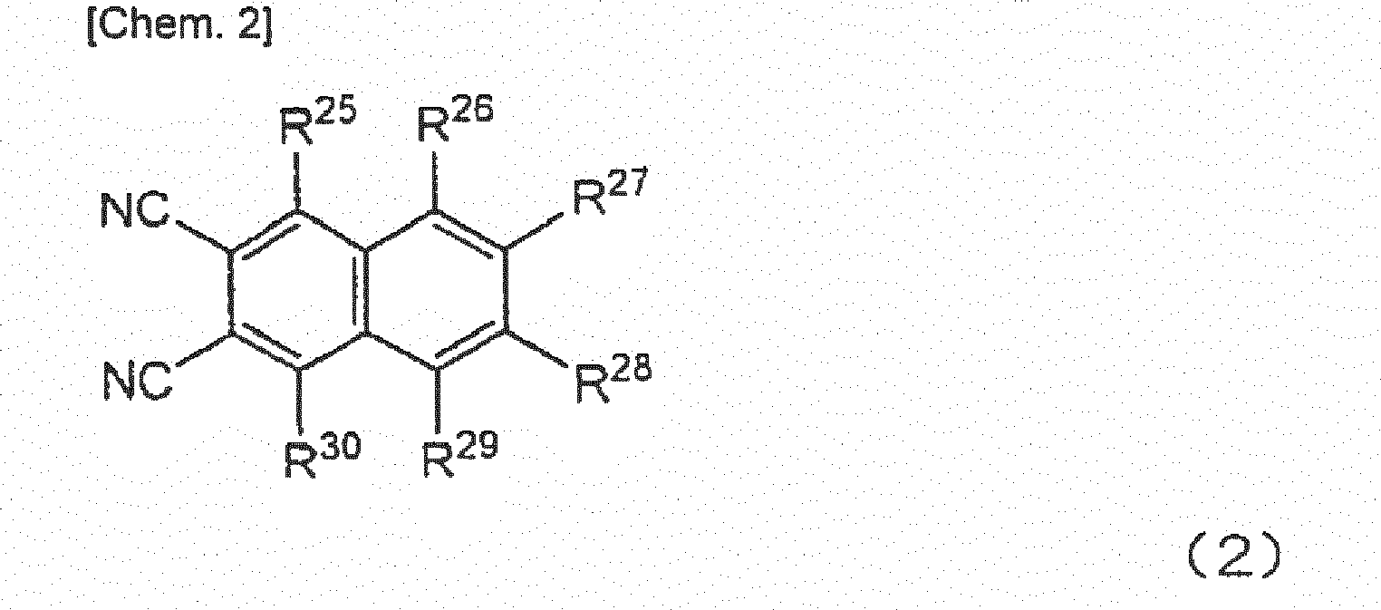
- In the tin naphthalocyanine represented by general formula (1) above, it is beneficial, in terms of ease of controlling the cohesion state of the molecules, that at least eight of R1 to R24 are each a hydrogen atom or a deuterium atom. It is more beneficial that at least sixteen of R1 to R24 are each a hydrogen atom or a deuterium atom, and it is still more beneficial that all of R1 to R24 are each a hydrogen atom or a deuterium atom. Tin naphthalocyanine represented by formula (3) below is advantageous in terms of ease of synthesis.


- The tin naphthalocyanine represented by general formula (1) above exhibits absorption in the wavelength range of from about 200 nm to 1,100 nm inclusive. The absorption peak of tin naphthalocyanine can be located at a wavelength of about 940 nm. The tin naphthalocyanine represented by formula (3) above has an absorption peak at a wavelength of about 870 nm as shown in
Fig. 5. Fig. 5 is an example of the absorption spectrum in a photoelectric conversion layer containing the tin naphthalocyanine represented by formula (3) above. The quantum efficiency of the photoelectric conversion layer containing the tin naphthalocyanine represented by formula (3) at a wavelength of 900 nm can be about 10 times higher than that of silicon. In the measurement of the absorption spectrum, a sample in which the photoelectric conversion layer (thickness: 30 nm) was stacked on a quartz substrate was used. - As can be seen from
Fig. 5 , the photoelectric conversion layer formed from a material containing the tin naphthalocyanine exhibits absorption in the near infrared region. Specifically, by selecting the material containing the tin naphthalocyanine as the material forming thephotoelectric conversion layer 23A, a photosensor capable of detecting near infrared rays can be obtained. In this embodiment of the present disclosure, by using an appropriate material suitable for an intended detection wavelength range, a photosensor having sensitivity in the desired wavelength range can be obtained. For example, P3HT (poly(3-hexylthiophene-2,5-diyl)), which is an example of an organic p-type semiconductor compound, has an absorption peak at a wavelength of 550 nm, and copper phthalocyanine has absorption peaks at wavelengths of 620 nm and 700 nm. - No particular limitation is imposed on the material for forming the
photoelectric conversion layer 23A so long as the material can generate electric charges by absorption of light. Thephotoelectric conversion layer 23A may be formed from an organic p-type semiconductor (compound) described later or may be formed from an organic n-type semiconductor (compound) described later. Alternatively, a combination of an organic p-type semiconductor (compound) and an organic n-type semiconductor (compound) may be used to form thephotoelectric conversion layer 23A. Thephotoelectric conversion layer 23A may contain an inorganic semiconductor material such as amorphous silicon. Thephotoelectric conversion layer 23A may include a layer formed from an organic material and a layer formed from an inorganic material. -
Fig. 6 shows an example of the structure of a photodetection element including a photoelectric conversion layer formed using an organic semiconductor material containing the tin naphthalocyanine represented by general formula (1) above. Adielectric structure 2B in thephotodetection element 10B shown inFig. 6 includes ahole blocking layer 20h, aphotoelectric conversion layer 23B, and anelectron blocking layer 20e. In the structure exemplified inFig. 6 , thehole blocking layer 20h is disposed between afirst electrode 21 and thephotoelectric conversion layer 23B, and theelectron blocking layer 20e is disposed between thephotoelectric conversion layer 23B and asecond electrode 22. - The
photoelectric conversion layer 23B contains at least one of a p-type semiconductor and an n-type semiconductor. In the structure exemplified inFig. 6 , thephotoelectric conversion layer 23B includes a p-type semiconductor layer 230p, an n-type semiconductor layer 230n, and amixed layer 230h sandwiched between the p-type semiconductor layer 230p and the n-type semiconductor layer 230n. The p-type semiconductor layer 230p is disposed between thehole blocking layer 20h and themixed layer 230h and functions as a photoelectric conversion layer and/or a hole transport layer. The n-type semiconductor layer 230n is disposed between themixed layer 230h and theelectron blocking layer 20e and functions as a photoelectric conversion layer and/or an electron transport layer. As described later, themixed layer 230h contains a p-type semiconductor and an n-type semiconductor. - The p-
type semiconductor layer 230p and the n-type semiconductor layer 230n contain an organic p-type semiconductor and an organic n-type semiconductor, respectively. Thephotoelectric conversion layer 23B may contain an organic photoelectric conversion material containing the tin naphthalocyanine represented by general formula (1) above and at least one of an organic p-type semiconductor and an organic n-type semiconductor. - The organic p-type semiconductor (compound) is a donating organic semiconductor (compound) typified mainly by a hole transport organic compound and is an organic compound having the property of easily donating electrons. More specifically, when two organic materials in contact with each other are used, one of the organic materials that has a lower ionization potential is an organic p-type semiconductor (compound). Therefore, any organic compound having the ability to donate electrons can be used as the donating organic compound. Examples of the organic compound that can be used include triarylamine compounds, benzidine compounds, pyrazoline compounds, styrylamine compounds, hydrazone compounds, triphenylmethane compounds, carbazole compounds, polysilane compounds, thiophene compounds such as P3HT, phthalocyanine compounds such as copper phthalocyanine, cyanine compounds, merocyanine compounds, oxonol compounds, polyamine compounds, indole compounds, pyrrole compounds, pyrazole compounds, polyarylene compounds, condensed aromatic carbocyclic compounds (naphthalene derivatives, anthracene derivatives, phenanthrene derivatives, tetracene derivatives, pyrene derivatives, perylene derivatives, and fluoranthene derivatives), and metal complexes containing a nitrogen-containing heterocyclic compound as a ligand. The donating organic semiconductor is not limited to these compounds, and any other organic compound that has a lower ionization potential than an organic compound used as the n-type (accepting) compound can be used as the donating organic semiconductor, as described above. The tin naphthalocyanine described above is an example of the organic p-type semiconductor material.
- The organic n-type semiconductor (compound) is an accepting organic semiconductor (compound) typified mainly by an electron transport organic compound and is an organic compound having the property of easily accepting electrons. More specifically, when two organic materials in contact with each other are used, one of the organic materials that has a higher electron affinity is an organic n-type semiconductor (compound). Therefore, any organic compound having the ability to accept electrons can be used as the accepting organic compound. Examples of the organic compound that can be used include fullerenes, fullerene derivatives such as phenyl-C61-butyric acid methyl ester (PCBM), condensed aromatic carbocyclic compounds (naphthalene derivatives, anthracene derivatives, phenanthrene derivatives, tetracene derivatives, pyrene derivatives, perylene derivatives, and fluoranthene derivatives), 5- to 7-membered nitrogen, oxygen, and/or sulfur atom-containing heterocyclic compounds (such as pyridine, pyrazine, pyrimidine, pyridazine, triazine, quinoline, quinoxaline, quinazoline, phthalazine, cinnoline, isoquinoline, pteridine, acridine, phenazine, phenanthroline, tetrazole, pyrazole, imidazole, thiazole, oxazole, indazole, benzimidazole, benzotriazole, benzoxazole, benzothiazole, carbazole, purine, triazolopyridazine, triazolopyrimidine, tetrazaindene, oxadiazole, imidazopyridine, pyrrolopyridine, thiadiazolopyridine, dibenzazepine, and tribenzazepine), polyarylene compounds, fluorene compounds, cyclopentadiene compounds, silyl compounds, perylenetetracarboxylic diimide (PTCDI) compounds, and metal complexes containing a nitrogen-containing heterocyclic compound as a ligand. The accepting organic semiconductor is not limited to these compounds, and any other organic compound that has a higher electron affinity than an organic compound used as the p-type (donating) compound can be used as the accepting organic semiconductor, as described above.
- When the
dielectric structure 2B has thephotoelectric conversion layer 23B including the p-type semiconductor layer 230p and the n-type semiconductor layer 230n as exemplified inFig. 6 , holes and electrons generated by photoelectric conversion can be easily separated from each other. Therefore, when thephotoelectric conversion layer 23B including the p-type semiconductor layer 230p and the n-type semiconductor layer 230n is used, the efficiency of charge separation is improved, and a change in the intensity of incident light can cause a larger change in permittivity. - The
mixed layer 230h may be, for example, a bulk heterojunction structure layer containing a p-type semiconductor and an n-type semiconductor. When themixed layer 230h is formed as a layer having the bulk heterojunction structure, the tin naphthalocyanine represented by general formula (1) above may be used as the p-type semiconductor material. The n-type semiconductor material used may be a fullerene and/or a fullerene derivative. The details of the bulk heterojunction structure are described in Japanese Patent No.5553727 5553727 - The material used to form the
hole blocking layer 20h may be an n-type semiconductor or an electron transport organic compound. Examples of such materials include: organic materials and organic-metal compounds such as fullerenes, e.g., C60 and C70, fullerene derivatives, e.g., indene-C60 bisadduct (ICBA), carbon nanotubes and derivatives thereof, oxadiazole derivatives, e.g., OXD-7 (1,3-bis(4-tert-butylphenyl-1,3,4-oxadiazolyl)phenylene), anthraquinodimethane derivatives, diphenylquinone derivatives, bathocuproine (BCP), bathophenanthroline and derivatives thereof, distyrylarylene derivatives, triazole compounds, silole compounds, a tris(8-hydroxyquinolinato)aluminum complex, a bis(4-methyl-8-quinolinato)aluminum complex, acetylacetonate complexes, copper phthalocyanine, 3,4,9,10-perylenetetracarboxylic dianhydride (PTCDA), and Alq; and inorganic materials such as MgAg and MgO. The material used to form thehole blocking layer 20h may be selected from the above materials in consideration of the ionization potential of the material forming thephotoelectric conversion layer 23A (or the p-type semiconductor layer 230p in thephotoelectric conversion layer 23B). - In a structure in which light enters the
photoelectric conversion layer 23B (or thephotoelectric conversion layer 23A) from thefirst electrode 21 side, it is beneficial when the transmittance of thehole blocking layer 20h in the intended detection wavelength range is high. For example, thehole blocking layer 20h may be reduced in thickness. Thehole blocking layer 20h may have a thickness within the range of, for example, from 5 nm to 50 nm inclusive. - The material used to form the
electron blocking layer 20e may be a p-type semiconductor or a hole transport organic compound. Examples of such materials include aromatic diamine compounds such as TPD (N,N'-bis(3-methylphenyl)-(1,1'-biphenyl)-4,4'-diamine) and α-NPD (4,4'-bis[N-(naphthyl)-N-phenyl-amino]biphenyl), oxazole, oxadiazole, triazole, imidazole, imidazolone, stilbene derivatives, pyrazoline derivatives, tetrahydroimidazole, polyarylalkanes, butadiene, m-MTDATA (4,4',4"-tris(N-(3-methylphenyl)N-phenylamino)triphenylamine), perylene, porphyrin compounds such as porphine, copper tetraphenylporphine, phthalocyanine, copper phthalocyanine, and titanium phthalocyanine oxide, triazole derivatives, oxadiazole derivatives, imidazole derivatives, polyarylalkane derivatives, pyrazoline derivatives, pyrazolone derivatives, phenylenediamine derivatives, arylamine derivatives, amino-substituted chalcone derivatives, oxazole derivatives, styrylanthracene derivatives, fluorenone derivatives, hydrazone derivatives, and silazane derivatives. The material used to form theelectron blocking layer 20e may be: polymers of phenylenevinylene, fluorene, carbazole, indole, pyrene, pyrrole, picoline, thiophene, acetylene, and diacetylene; and derivatives thereof. The material used to form theelectron blocking layer 20e is selected from the above materials in consideration of the electron affinity of thephotoelectric conversion layer 23A (or the n-type semiconductor layer 230n in thephotoelectric conversion layer 23B). - In a structure in which light enters the
photoelectric conversion layer 23B (or thephotoelectric conversion layer 23A) from thesecond electrode 22 side, it is beneficial when the transmittance of theelectron blocking layer 20e in the intended detection wavelength range is high. For example, theelectron blocking layer 20e may be reduced in thickness. Theelectron blocking layer 20e may have a thickness within the range of, for example, from 5 nm to 50 nm inclusive. - By selecting an appropriate combination of the materials of the
first electrode 21, the photoelectric conversion layer (thephotoelectric conversion layer second electrode 22, one of thehole blocking layer 20h and theelectron blocking layer 20e can be omitted. Examples of such a structure will next be described. -
Fig. 7 is an exemplary energy diagram of a photodetection element in which thehole blocking layer 20h and aphotoelectric conversion layer 23C are disposed between thefirst electrode 21 and thesecond electrode 22. As illustrated, in this example, thephotoelectric conversion layer 23C is adjacent to thesecond electrode 22 to which the second voltage is applied. Specifically,Fig. 7 shows a structural example in which theelectron blocking layer 20e is omitted. In the example described here, thephotoelectric conversion layer 23C has a heterojunction structure between the p-type semiconductor layer 230p and the n-type semiconductor layer 230n. Of course, thephotoelectric conversion layer 23C may have a bulk heterojunction structure. - In the structure exemplified in
Fig. 7 , as in thephotodetection element 10A described with reference toFigs. 2 and3 , thehole blocking layer 20h suppresses movement of holes from thephotoelectric conversion layer 23C to thefirst electrode 21. In the structure exemplified inFig. 7 , the difference between the LUMO of thehole blocking layer 20h and the Fermi level of thefirst electrode 21 is large, and therefore a potential barrier for electrons is formed between thefirst electrode 21 and thehole blocking layer 20h. The potential barrier suppresses movement of electrons from thefirst electrode 21 to thehole blocking layer 20h. In other words, transport of electrons from thefirst electrode 21 to thehole blocking layer 20h is suppressed without using an electron blocking layer. - In the structure in which the photoelectric conversion layer (the
photoelectric conversion layer 23C in this case) and an electrode (thesecond electrode 22 in this case) are disposed adjacent to each other, it is known that, when the difference between the work function of the electrode and the ionization potential of the organic film adjacent to the electrode is large, holes are unlikely to enter the organic film from the electrode. In the structure exemplified inFig. 7 , the ionization potential of thephotoelectric conversion layer 23C is higher than the work function of thesecond electrode 22, and the difference between the HOMO of thephotoelectric conversion layer 23C and the Fermi level of thesecond electrode 22 is relatively large. Therefore, the potential barrier between thephotoelectric conversion layer 23C and thesecond electrode 22 suppresses injection of holes from thesecond electrode 22 into thephotoelectric conversion layer 23C. - As described above, also by suppressing movement of positive charges or negative charges (holes in this case) generated by photoelectric conversion to an electrode (the
first electrode 21 in this case), the charges generated by photoelectric conversion can be retained within thephotoelectric conversion layer 23C. Specifically, even though theelectron blocking layer 20e is not provided, the permittivity can be changed in response to irradiation with light when the materials of thefirst electrode 21, thehole blocking layer 20h, thephotoelectric conversion layer 23C, and thesecond electrode 22 are appropriately selected such that the relative relations among the energies of the components of the photodetection element are as shown inFig. 7 . - One example of the combination of the materials that can satisfy the relative relations among the energies of the components of the photodetection element in
Fig. 7 is as follows. -
- First electrode 21: ITO (WF: 4.7 eV)
-
Hole blocking layer 20h: ICBA (IP: 6.5 eV, EA: 3.7 eV) - p-
Type semiconductor layer 230p: copper phthalocyanine (IP: 5.2 eV, EA: 3.5 eV) - n-
Type semiconductor layer 230n: C60 (IP: 6.2 eV, EA: 4.5 eV) - Second electrode 22: Al (WF: 4.2 eV)
-
Fig. 8 schematically shows the relative relations among the energies obtained by the above combination. InFig. 8 , an arrow φ1 represents a potential barrier for electrons between thehole blocking layer 20h and thefirst electrode 21, and an arrow φ2 represents a potential barrier for holes between the n-type semiconductor layer 230n and thesecond electrode 22. An arrow φ3 represents a potential barrier for holes between the p-type semiconductor layer 230p and thehole blocking layer 20h. Of course, the above combination is merely an example. For example, P3HT, tin naphthalocyanine, etc. may be used instead of copper phthalocyanine exemplified as the material of the p-type semiconductor layer 230p. -
Fig. 9 is an exemplary energy diagram of a photodetection element in which thephotoelectric conversion layer 23C and theelectron blocking layer 20e are disposed between thefirst electrode 21 and thesecond electrode 22. As illustrated, in this example, thephotoelectric conversion layer 23C is adjacent to thefirst electrode 21 to which the first voltage is applied. Specifically,Fig. 9 shows a structural example in which thehole blocking layer 20h is omitted. - In the example illustrated, as in the
photodetection element 10A described with reference toFigs. 2 and3 , theelectron blocking layer 20e suppresses movement of electrons from thephotoelectric conversion layer 23C to thesecond electrode 22. In the structure exemplified inFig. 9 , the difference between the HOMO of theelectron blocking layer 20e and the Fermi level of thesecond electrode 22 is large, and a potential barrier for holes is formed between theelectron blocking layer 20e and thesecond electrode 22. This potential barrier suppresses movement of holes from thesecond electrode 22 to theelectron blocking layer 20e. In other words, transport of holes from thesecond electrode 22 to theelectron blocking layer 20e is suppressed without using a hole blocking layer. - In the structure in which the photoelectric conversion layer (the
photoelectric conversion layer 23C in this case) and an electrode (thefirst electrode 21 in this case) are disposed adjacent to each other, when the difference between the work function of the electrode and the electron affinity of the organic film adjacent to the electrode is large, electrons are unlikely to be injected into the organic film from the electrode. In the structure exemplified inFig. 9 , the electron affinity of thephotoelectric conversion layer 23C is lower than the work function of thefirst electrode 21, and the difference between the Fermi level of thefirst electrode 21 and the LUMO of thephotoelectric conversion layer 23C is relatively large. Therefore, a potential barrier is formed between thefirst electrode 21 and thephotoelectric conversion layer 23C. This potential barrier suppresses injection of electrons from thefirst electrode 21 into thephotoelectric conversion layer 23C. As described above, even though thehole blocking layer 20h is not provided, the permittivity can be changed in response to irradiation with light when the materials of thefirst electrode 21, thephotoelectric conversion layer 23C, theelectron blocking layer 20e, and thesecond electrode 22 are appropriately selected such that the relative relations among the energies of the components of the photodetection element are as shown inFig. 9 . - One example of the combination of the materials of the
first electrode 21, thephotoelectric conversion layer 23C, theelectron blocking layer 20e, and thesecond electrode 22 that are combined so as to satisfy the relative relations among the energies of the components of the photodetection element inFig. 9 is as follows. -
- First electrode 21: ITO (WF: 4.7 eV)
- p-
Type semiconductor layer 230p: copper phthalocyanine (IP: 5.2 eV, EA: 3.5 eV) - n-
Type semiconductor layer 230n: C60 (IP: 6.2 eV, EA: 4.5 eV) -
Electron blocking layer 20e: perylene (IP: 5.3 eV, EA: 2.3 eV) - Second electrode 22: Al (WF: 4.2 eV)
-
Fig. 10 schematically shows the relative relations among the energies obtained by the above combination. InFig. 10 , an arrow φ5 represents a potential barrier for electrons between thefirst electrode 21 and the p-type semiconductor layer 230p. An arrow φ6 represents a potential barrier for holes between theelectron blocking layer 20e and thesecond electrode 22, and an arrow φ7 represents a potential barrier for electrons between the n-type semiconductor layer 230n and theelectron blocking layer 20e. P3HT, tin naphthalocyanine, etc. may be used instead of copper phthalocyanine exemplified below. Copper phthalocyanine may be used instead of perylene exemplified as the material of theelectron blocking layer 20e. - As described above, the photodetection element in which the
hole blocking layer 20h or theelectron blocking layer 20e is omitted can also suppress movement of electric charges generated by photoelectric conversion to the electrodes. In other words, the same effects as those of the photodetection element having both thehole blocking layer 20h and theelectron blocking layer 20e can be obtained using the simpler structures. It should be noted that, in the photodetection element in which one of thehole blocking layer 20h and theelectron blocking layer 20e is disposed in the dielectric structure, the position of the interposed blocking layer (thehole blocking layer 20h or theelectron blocking layer 20e) is determined according to which of the two electrodes is at a higher electric potential under the application of voltage. - In terms of suppressing movement of electric charges generated by photoelectric conversion to the electrodes, an insulating layer that does not allow holes and electron to pass through may be used instead of the
hole blocking layer 20h and/or theelectron blocking layer 20e. A description will be given of an example of the structure in which an insulating layer is disposed between a photoelectric conversion layer and electrodes. -
Fig. 11 shows the outline of an exemplary structure of a photosensor according to a second embodiment of the present disclosure. The photosensor 100C shown inFig. 11 includes: aphotodetection element 10C including a dielectric structure 2C disposed between afirst electrode 21 and asecond electrode 22; and avoltage supply circuit 12. The dielectric structure 2C includes an insulatinglayer 29a and an insulatinglayer 29b. As illustrated, the insulatinglayer 29a is disposed between thefirst electrode 21 and thephotoelectric conversion layer 23C. The insulatinglayer 29b is disposed between thephotoelectric conversion layer 23C and thesecond electrode 22. -
Fig. 12 is an exemplary energy diagram of thephotodetection element 10C. InFig. 12 , the base of the leftmost one of three rectangles represents the upper edge of the valence band of the insulatinglayer 29a, and the side opposite to the base represents the bottom of its conduction band. Similarly, the rightmost rectangle inFig. 12 schematically shows the energy levels of the upper edge of the valence band of the insulatinglayer 29b and the bottom of its conduction band. In the following description, the difference between the upper edge of a valence band and the vacuum level and the difference between the bottom of a conduction band and the vacuum level may be represented by VB and CB, respectively. - By disposing the insulating
layer 29a between thefirst electrode 21 and thephotoelectric conversion layer 23C, movement of electric charges between thefirst electrode 21 and thephotoelectric conversion layer 23C can be suppressed even when a voltage is applied between thefirst electrode 21 and thesecond electrode 22. By disposing the insulatinglayer 29b between thesecond electrode 22 and thephotoelectric conversion layer 23C, movement of electric charges between thesecond electrode 22 and thephotoelectric conversion layer 23C can be suppressed. Therefore, the electric charges generated by photoelectric conversion are suppressed from migrating to the electrodes (thefirst electrode 21 and/or the second electrode 22) and can be used as electric charges contributing to a change in the permittivity of the dielectric structure 2C. The "insulating layers" as used herein are distinguished from thehole blocking layer 20h and theelectron blocking layer 20e because the insulating layers block the movement of both the positive and negative charges irrespective of the direction of the electric field applied from the outside. In other words, the "insulating layers" as used herein suppress both the positive and negative charges from migrating from the electrodes to the photoelectric conversion layer and from migrating from the photoelectric conversion layer to the electrodes. - The material used to form the insulating
layers layers layer 29a and/or the insulatinglayer 29b. It is beneficial that a so-called high-permittivity material (referred to also as a high-k material and having a relative permittivity of typically more than 3.9) is used to form the insulatinglayer 29a and/or the insulatinglayer 29b. The thicknesses of the insulatinglayer 29a and the insulatinglayer 29b may be appropriately set according to the electric conductivities of the insulatinglayer 29a and the insulatinglayer 29b. - In the structure exemplified in
Figs. 11 and12 , the insulatinglayer 29a is disposed between thefirst electrode 21 and thephotoelectric conversion layer 23C. Moreover, the insulatinglayer 29b is disposed between thephotoelectric conversion layer 23C and thesecond electrode 22. Therefore, during operation of the photosensor 100C, any one of thefirst electrode 21 and thesecond electrode 22 may be at a higher potential than the other. Specifically, the structure exemplified inFig. 11 has an advantage in that less restrictions are imposed on the material of thefirst electrode 21 and the material of thesecond electrode 22. For example, when thesecond electrode 22 is a transparent electrode, the material used for thesecond electrode 22 may be a transparent conductive oxide (TCO) such as ITO, IZO, AZO, FTO, SnO2, TiO2, or ZnO2, a carbon nanotube, graphene, etc. When thefirst electrode 21 is a transparent electrode, the material used for thesecond electrode 22 may be Al, TiN, Cu, TaN, etc. The material used for thefirst electrode 21 may be selected from the same materials as those for thesecond electrode 22. For example, the material used for thefirst electrode 21 may be Al, TiN, Cu, TaN, ITO, etc. - As described below, one of the insulating
layers first electrode 21, thephotoelectric conversion layer 23C (or thephotoelectric conversion layer second electrode 22. -
Fig. 13 is an exemplary energy diagram of a photodetection element in which the insulatinglayer 29a and thephotoelectric conversion layer 23C are disposed between thefirst electrode 21 and thesecond electrode 22. As illustrated, in this example, thephotoelectric conversion layer 23C is adjacent to thesecond electrode 22 to which the second voltage is applied. Specifically,Fig. 13 shows a structural example in which the insulatinglayer 29b is omitted. - In the structure exemplified in
Fig. 13 , the insulatinglayer 29a suppresses movement of holes from thephotoelectric conversion layer 23C to thefirst electrode 21 and movement of electrons from thefirst electrode 21 to thephotoelectric conversion layer 23C. In this example, the ionization potential of thephotoelectric conversion layer 23C is set to be larger than the work function of thesecond electrode 22. Therefore, injection of holes from thesecond electrode 22 into thephotoelectric conversion layer 23C is suppressed by the potential barrier between thephotoelectric conversion layer 23C and thesecond electrode 22. In this case, part of electric charges (e.g., holes) generated by photoelectric conversion can be retained within thephotoelectric conversion layer 23C and can be utilized as electric charges contributing to a change in the permittivity of thephotoelectric conversion layer 23C. As described above, even though the insulatinglayer 29b is not provided between thephotoelectric conversion layer 23C and thesecond electrode 22, movement of electric charges generated by photoelectric conversion to the electrodes can be suppressed by appropriately selecting the materials of thefirst electrode 21, the insulatinglayer 29a, thephotoelectric conversion layer 23C, and thesecond electrode 22 such that the relative relations among the energies of the components of the photodetection element are as shown inFig. 13 . - One example of the combination of the materials that can satisfy the relative relations among the energies of the components of the photodetection element in
Fig. 13 is as follows. -
- First electrode 21: ITO (WF: 4.7 eV)
- Insulating
layer 29a: Al2O3 (VB: 10.0 eV, CB: 1.2 eV) - p-
Type semiconductor layer 230p: copper phthalocyanine (IP: 5.2 eV, EA: 3.5 eV) - n-
Type semiconductor layer 230n: C60 (IP: 6.2 eV, EA: 4.5 eV) - Second electrode 22: Al (WF: 4.2 eV)
-
Fig. 14 schematically shows the relative relations among the energies obtained by the above combination. The material used for thesecond electrode 22 may be a metal having a work function of from about 4.1 eV to about 4.3 eV inclusive. Therefore, instead of Al exemplified below, Ti, Ta, Ag, etc. may be used. The material used for the n-type semiconductor layer 230n adjacent to thesecond electrode 22 may be a material having an ionization potential of about 5 eV or more. Instead of Al2O3 exemplified as the material of the insulatinglayer 29a, SiO2, ZrO2, HfO2, Y2O3, etc. may be used. -
Fig. 15 is an exemplary energy diagram of a photodetection element in which thephotoelectric conversion layer 23C and the insulatinglayer 29b are disposed between thefirst electrode 21 and thesecond electrode 22. As illustrated, in this example, thephotoelectric conversion layer 23C is adjacent to thefirst electrode 21 to which the first voltage is applied. Specifically,Fig. 15 shows an example in which the insulatinglayer 29a is omitted. - In the structure exemplified in
Fig. 15 , the insulatinglayer 29b blocks movement of electrons from thephotoelectric conversion layer 23C to thesecond electrode 22 and movement of holes from thesecond electrode 22 to thephotoelectric conversion layer 23C. In this example, the electron affinity of thephotoelectric conversion layer 23C is set to be lower than the work function of thefirst electrode 21. In this case, injection of electrons from thefirst electrode 21 into thephotoelectric conversion layer 23C is suppressed by the potential barrier between thefirst electrode 21 and thephotoelectric conversion layer 23C. Therefore, also in the above structure, part of electric charges (e.g., electrons) generated by photoelectric conversion can be retained within thephotoelectric conversion layer 23C and can be used as electric charges contributing to a change in the permittivity of thephotoelectric conversion layer 23C. As described above, even though the insulatinglayer 29a is not provided between thefirst electrode 21 and thephotoelectric conversion layer 23C, movement of electric charges generated by photoelectric conversion to the electrodes can be suppressed by appropriately selecting the materials of thefirst electrode 21, thephotoelectric conversion layer 23C, the insulatinglayer 29b, and thesecond electrode 22 such that the relative relations among the energies of the components of the photodetection element are as shown inFig. 15 . - One example of the combination of the materials that can satisfy the relative relations among the energies of the components of the photodetection element in
Fig. 15 is as follows. -
- First electrode 21: Au (WF: 4.9 eV)
- p-
Type semiconductor layer 230p: copper phthalocyanine (IP: 5.2 eV, EA: 3.5 eV) - n-
Type semiconductor layer 230n: C60 (IP: 6.2 eV, EA: 4.5 eV) - Insulating
layer 29b: Al2O3 (VB: 10.0 eV, CB: 1.2 eV) - Second electrode 22: ITO (WF: 4.7 eV)
-
Fig. 16 schematically shows the relative relations among the energies obtained by the above combination. The material used for thefirst electrode 21 may be a metal having a work function of about 4.8 eV or more. For example, instead of Au exemplified below, Pt, Ni, ITO, etc. may be used. - An example of the change in the permittivity of a photoelectric conversion layer due to light irradiation will be described with reference to an Example.
Fig. 17 schematically shows the structure of a photodetection element used for measurement of the change in permittivity. Thephotodetection element 10D having the structure shown inFig. 17 was produced using the following procedure. - First, a glass substrate 2GL was prepared. Next, ITO was deposited on the glass substrate 2GL by sputtering to thereby form an ITO electrode (thickness: 50 nm) serving as a
second electrode 22. Next, atomic layer deposition (ALD) was used to form a HfO2 layer (thickness: 30 nm) serving as an insulatinglayer 29b on thesecond electrode 22. Then tin naphthalocyanine and C60 were co-evaporated to form a co-evaporated layer (thickness: 150 nm) serving as aphotoelectric conversion layer 23D on the insulatinglayer 29b. - Next, ALD was used to form an Al2O3 layer (thickness: 30 nm) serving as an insulating
layer 29a on thephotoelectric conversion layer 23D. Then sputtering was used to deposit Al on the insulatinglayer 29a to thereby form an Al electrode (thickness: 80 nm) serving as afirst electrode 21. Through the above steps, aphotodetection element 10D having the structure shown inFig. 17 was obtained. The shape of thephotoelectric conversion layer 23D was a rectangle with 1 mm sides when viewed in a direction normal to the glass substrate 2GL. - In this example, an LED light source (wavelength: 940 nm, rated power consumption: about 70 mW) was used. As schematically shown in
Fig. 17 , a measuringapparatus 300 was connected to thefirst electrode 21 and thesecond electrode 22 to apply a potential difference of 4 V between thefirst electrode 21 and thesecond electrode 22. In this state, the capacitance value of adielectric structure 2D between thefirst electrode 21 and thesecond electrode 22 was measured. To measure the capacitance value, a semiconductor device parameter analyzer B1500A (measurement frequency: 1 kHz, amplitude: 0.1 V) manufactured by Keysight was used. During the measurement, a LOW side of a probe of the measuring apparatus was brought into contact with thefirst electrode 21, and a HIGH side of the probe was brought into contact with thesecond electrode 22. -
Fig. 18 shows the results of the measurement of the capacitance value of thedielectric structure 2D. InFig. 18 , open squares (□) show the results of the capacitance value measurement when thephotoelectric conversion layer 23D was not irradiated with light (LED light source: off, dark condition). Open triangles (Δ) show the results of the capacitance value measurement when thephotoelectric conversion layer 23D was irradiated with light (LED light source: on). As shown inFig. 18 , the capacitance value without light irradiation was about 6.3 µF, and the capacitance value under light irradiation was about 2 µF. Therefore, in this example, when thephotoelectric conversion layer 23D was irradiated with light, the capacitance value of thedielectric structure 2D was increased by a factor of about 3 as compared to that in the dark condition. - Changes in the capacitance value of the
dielectric structure 2D were measured with a potential difference of 4 V applied between thefirst electrode 21 and thesecond electrode 22 while the LED light source was repeatedly turned on and off at one second intervals. InFig. 18 , open diamonds (◊) show the results of the capacitance value measurement when the LED light source was repeatedly turned on and off at one second intervals. As shown inFig. 18 , when light enters thephotoelectric conversion layer 23D, the capacitance value of thedielectric structure 2D increases steeply. When the LED light source is turned off, the capacitance value of thedielectric structure 2D decreases steeply. - As described above, according to this embodiment of the present disclosure, a photosensor in which the capacitance value between its electrodes changes in response to a change in illuminance can be obtained.
- Next, referring to the drawings, a description will be given of specific examples of the device structure of the photodetection element capable of generating a signal that corresponds to a change in permittivity due to irradiation with light.
-
Fig. 19 shows an example of the device structure of the photodetection element. Thephotodetection element 10E shown inFig. 19 is supported by asubstrate 2. Thesubstrate 2 used may be, for example, a silicon substrate having an oxide film on its surface, a glass substrate, or a polyimide substrate. In the example illustrated, asecond electrode 22 is disposed on thesubstrate 2. - In the structure exemplified in
Fig. 19 , adielectric structure 2E disposed between afirst electrode 21 and thesecond electrode 22 includes barrier layers B1 and B2 and aphotoelectric conversion layer 23A. The barrier layer B1 disposed between thefirst electrode 21 and thephotoelectric conversion layer 23A may be thehole blocking layer 20h described above or the insulatinglayer 29a described above. Specifically, the barrier layer B1 is a layer having the function of suppressing at least transport of holes from the photoelectric conversion layer (thephotoelectric conversion layer 23A in this case) to thefirst electrode 21. The barrier layer B2 disposed between thephotoelectric conversion layer 23A and thesecond electrode 22 may be theelectron blocking layer 20e described above or the insulatinglayer 29b described above. Specifically, the barrier layer B2 is a layer having the function of suppressing at least transport of electrons from the photoelectric conversion layer (thephotoelectric conversion layer 23A in this case) to thesecond electrode 22. - By employing the capacitor structure exemplified in
Fig. 19 , light entering thephotoelectric conversion layer 23A can be detected as a change in the capacitance value between thefirst electrode 21 and thesecond electrode 22. The light may enter from thefirst electrode 21 side or may enter from thesecond electrode 22 side. For example, when thefirst electrode 21 is a transparent electrode, the light may enter thephotoelectric conversion layer 23A through thefirst electrode 21. Alternatively, when thesubstrate 2 is a transparent substrate and thesecond electrode 22 is a transparent electrode, the light may enter thephotoelectric conversion layer 23A through thesubstrate 2 and thesecond electrode 22. - In
Fig. 19 , the voltage supply circuit 12 (see, for example,Fig. 2 ) is not illustrated and is omitted. In the structure in which the photodetection element (thephotodetection element 10E in this case) is supported by the substrate (thesubstrate 2 in this case) as exemplified inFig. 19 , thevoltage supply circuit 12 may be disposed on the substrate. - The change in the capacitance value between the
first electrode 21 and thesecond electrode 22 may be detected, for example, in the following manner. First, an AC voltage is applied between theelectrodes electrodes electrodes 
- When the equivalent circuit between the
electrodes 
- In actual measurement, an appropriate one of the above two formulas can be selected according to the structure of the element and the frequency of the AC voltage.
- A different detection method will be described with reference to
Fig. 22. Fig. 22 schematically shows a cross section of a photodetector including the capacitor structure of the present disclosure. - In
Fig. 22 , aphotosensor 100C includes atransistor 60 and a photoelectric conversion unit. Thetransistor 60 is a field effect transistor formed on asemiconductor substrate 20. Thetransistor 60 includes animpurity region 20d, animpurity region 20s, an insulatinglayer 23x on the semiconductor substrate, and agate electrode 24 on the insulatinglayer 23x. Theimpurity region 20d functions as a drain region (or a source region) of thetransistor 60, and theimpurity region 20s function as the source region (or the drain region) of thetransistor 60. Theimpurity region 20d is connected to apower source line 42, so that a prescribed voltage can be applied to theimpurity region 20d during operation of thephotodetector 1000. The insulatinglayer 23x functions as a gate insulating layer of thetransistor 60. The insulatinglayer 23x is, for example, a thermally oxidized silicon film having a thickness of 4.6 nm. - The photoelectric conversion unit of the photosensor 100C includes a
pixel electrode 21, atransparent electrode 22 facing thepixel electrode 21, and aphotoelectric conversion layer 23p sandwiched therebetween. An insulatinglayer 29a is disposed between thepixel electrode 21 and thephotoelectric conversion layer 23p, and an insulatinglayer 29b is disposed between thephotoelectric conversion layer 23p and thetransparent electrode 22. Thepixel electrode 21 is disposed so as to be spaced apart from adjacentunit pixel cells 10C. Therefore, thepixel electrode 21 is electrically isolated frompixel electrodes 21 of otherunit pixel cells 10C. Thepixel electrode 21 is typically a metal electrode or a metal nitride electrode. Examples of the material for forming thepixel electrode 21 include Al, Cu, Ti, TiN, Ta, TaN, Mo, Ru, and Pt. Thepixel electrode 21 may be formed from polysilicon doped with an impurity to impart electrical conductivity. In the above case, thepixel electrode 21 used is a TiN electrode. - For example, a material through which a smaller leakage current can flow than through the material forming the
photoelectric conversion layer 23p may be selected as the material forming the insulatinglayers layers - The
photoelectric conversion layer 23p is formed so as to extend over otherunit pixel cells 10C. The thickness of thephotoelectric conversion layer 23p may be, for example, about 200 nm. Thetransparent electrode 22 is formed using a transparent conducting oxide (TCO) so as to extend over otherunit pixel cells 10C. Thetransparent electrode 22 is connected to a gate voltage control line (not illustrated), so that a prescribed voltage can be applied to thetransparent electrode 22 during operation of thephotodetector 1000. - In the example illustrated, the
transparent electrode 22 and thephotoelectric conversion layer 23p are disposed above aninterlayer insulating layer 50, and thepixel electrode 21 of the photoelectric conversion unit is connected to thegate electrode 24 of the capacitance-modulatedtransistor 60 through aconnection portion 54 including part ofmultilayer wiring 40 and acontact plug 52. - In the example described, a first voltage applied to the
impurity region 20d is 1.2 V, and a second voltage applied to thetransparent electrode 22 is 3.7 V. Specifically, in this example, a potential difference of about 2.5 V is applied between theimpurity region 20d and thetransparent electrode 22. -
Fig. 23 shows the film thickness dependence of a leakage current flowing through the silicon oxide film when a voltage of 2.5 V is applied. As described above, in terms of maintaining the characteristics with no light irradiation, it is beneficial that the leakage current to the channel region of the capacitance-modulatedtransistor 60 is 1×10-11 A/cm2 or less. As shown inFig. 23 , in the case in which a voltage of 2.5 V is applied to the silicon oxide film, the leakage current through the silicon oxide film can be reduced to 1×10-11 A/cm2 or less when the thickness of the silicon oxide film is 5.4 nm or more. - When light enters the
photoelectric conversion layer 23p, hole-electron pairs are generated in thephotoelectric conversion layer 23p, and the permittivity of thephotoelectric conversion layer 23p changes. As the permittivity of thephotoelectric conversion layer 23p changes, the effective gate voltage of the capacitance-modulatedtransistor 60 changes, and a drain current in the capacitance-modulatedtransistor 60 changes. Therefore, the change in illuminance can be detected as, for example, a change in voltage in avertical signal line 46. - In another detection method, a fixed capacitor connected in series to the
electrode Fig. 19 is further provided. With a constant voltage applied between two electrodes not used for the mutual connection between the fixed capacitor and the electrode, an intermediate voltage between the capacitor structure and the fixed capacitor is read, whereby the change in illuminance can be detected. - The fixed capacitor has a structure in which an insulating material using an oxide film, a nitride film, or an organic film is sandwiched between two electrodes and a change in capacitance in response to light is small (the capacity can be regarded as a constant).
- To read the change in the capacitance of the capacitor structure efficiently, it is desirable to design the capacitor structure such that the initial capacitance value of the capacitor structure under the condition in which no light enters the capacitor structure is lower than the capacitance value of the fixed capacitor.
- It is also desirable to set the positional relation between the fixed capacitor and the capacitor structure such that the capacitor structure is disposed on the light incident side.
- Let the constant voltage applied be VG, the capacitance value of the capacitor structure be C1, and the capacitance value of the fixed capacitor be C2. Then the intermediate voltage can be represented by a formula below. Using this formula, the change in the capacitance of the capacitor structure due to the incident light can be read as a change in voltage.

- To read the voltage, a transistor can be used, and the signal can be read nondestructively through connection to the gate electrode side of the transistor.
- The photodetection element in the photosensor of the present disclosure can be configured as a three-terminal element. Other specific examples of the device structure of the photodetection element will be described with reference to
Figs. 20 and21 . -
Fig. 20 shows another example of the device structure of the photodetection element. Thephotodetection element 10F shown inFig. 20 has a device structure similar to the device structure of thephotodetection element 10E described with reference toFig. 19 . However, the structure exemplified inFig. 20 differs from thephotodetection element 10E shown inFig. 19 in that, instead of thefirst electrode 21, a semiconductor layer SL, an electrode Ed, and an electrode Es are disposed on the barrier layer B1. As illustrated, the electrode Ed and the electrode Es are disposed on the semiconductor layer SL so as to be spaced apart from each other. As can be seen fromFig. 20 , thephotodetection element 10F has the device structure similar to a bottom gate thin film transistor. Examples of the material forming the semiconductor layer SL include single-walled carbon nanotubes (SWCNTs), oxide semiconductors including In-Ga-Zn-O-based (IGZO) semiconductors, organic semiconductors such as pentacene and P3HT, and amorphous silicon. - For example, suppose that light enters the
photoelectric conversion layer 23A through thesubstrate 2 and thesecond electrode 22. In this case, when the first voltage is applied to one of the electrode Ed and the electrode Es and when the second voltage is applied to thesecond electrode 22, the permittivity of thedielectric structure 2E changes. When the permittivity of thedielectric structure 2E increases, electric charges are induced in the semiconductor layer SL, and a current flowing between the electrode Ed and the electrode Es changes. Therefore, a signal corresponding to the illuminance of the light can be taken from the other one of the electrodes Ed and Es to which the first voltage is not applied. -
Fig. 21 shows another example of the device structure of the photodetection element. As exemplified inFig. 21 , a device structure similar to a top gate thin film transistor can be used. In this example, a semiconductor layer SL is disposed so as to cover electrodes Ed and Es spaced apart from each other, and adielectric structure 2E is disposed on the semiconductor layer SL. Afirst electrode 21 is disposed on thedielectric structure 2E. - When light is detected using the
photodetection element 10G shown inFig. 21 , the first voltage is applied to, for example, thefirst electrode 21, and the second voltage is applied to one of the electrode Ed and the electrode Es. In this case, as in thephotodetection element 10F described above, a signal corresponding to the illuminance of the light can be taken from the other one of the electrodes Ed and Es to which the first voltage is not applied. - In the structure shown in
Fig. 20 , the placement positions of the barrier layers B1 and B2 may be exchanged. In this case, the electric potential at one of the electrode Ed and the electrode Es is set to be higher than the electric potential at thesecond electrode 22 during detection of light. Similarly, in the structure exemplified inFig. 21 , the placement positions of the barrier layers B1 and B2 may be exchanged. In this case, the electric potential at one of the electrode Ed and the electrode Es is set to be lower than the electric potential at thefirst electrode 21 during detection of light. In the semiconductor layer SL, carriers induced in a region sandwiched between the electrode Ed and the electrode Es may be electrons or may be holes. - As described above, in the embodiments of the present disclosure, electric charges generated by photoelectric conversion are retained in the photoelectric conversion layer and used as electric charges contributing to the change in the permittivity of the dielectric structure including the photoelectric conversion layer. In the embodiments of the present disclosure, movement of electric charges between the photoelectric conversion layer and the electrodes is suppressed. By using the photosensor according to any of the above embodiments, an electric signal corresponding to the change in permittivity due to light irradiation can be taken from the photosensor.
- In the structures exemplified in the above embodiments, the photoelectric conversion material exhibiting absorption in the infrared range is used for the photoelectric conversion layer. The photoelectric conversion material exhibiting absorption in the infrared range has a narrow bandgap, and therefore dark current increases as the number of thermally excited carriers increases and the value of electrical resistance decreases. Therefore, when the photoelectric conversion material exhibiting absorption in the infrared range is used as the material of the photoelectric conversion layer, a sufficient S/N ratio may not be obtained. However, in the embodiments of the present disclosure, since a barrier layer is disposed between the photoelectric conversion layer and at least one of the two electrodes, leakage to the electrode can be reduced. In addition, the potential barrier of the barrier layer can suppress injection of electric charges from the electrode to the photoelectric conversion layer. For example, by reading the change in permittivity when the potential difference between the electrodes is changed, fixed noise due to thermal excitation etc. can be removed. Therefore, a low-noise infrared photosensor can be obtained using the photoelectric conversion material exhibiting absorption in the infrared range.
- In the embodiments of the present disclosure, holes and electrons generated by photoelectric conversion are separated from each other by forming an electric field in the photoelectric conversion layer. Therefore, an organic compound in which the time until recombination of holes and electrons is generally relatively short can be relatively easily used as the material of the photoelectric conversion layer.
- As described above, according to the embodiments of the present disclosure, a photosensor having sensitivity in the infrared range can be obtained using a relatively simple structure, In the photosensor according to any of the embodiments of the present disclosure, infrared light is detected not through heat, and therefore it is not necessary to provide a cooling mechanism.
- The photosensor of the present disclosure is applicable to photodetectors, image sensors, etc. By appropriately selecting the material of the photoelectric conversion layer, an image can be acquired using infrared light. The photosensor that captures an image using infrared light can be used for, for example, security cameras, vehicle-mounted cameras, etc. A vehicle-mounted camera can be used for, for example, input into a controller in order to allow the vehicle to drive safely. The vehicle-mounted camera can also be used to assist the operator in order to allow the vehicle to drive safely.
-
- 2 substrate
- 2A to 2E dielectric structure
- 10A to 10G photodetection element
- 12 voltage supply circuit
- 20e electron blocking layer
- 20h hole blocking layer
- 21 first electrode
- 22 second electrode
- 23A to 23D photoelectric conversion layer
- 29a, 29b insulating layer
- 100A, 100C photosensor
- 230h mixed layer
- 230n n-type semiconductor layer
- 230p p-type semiconductor layer
- B1, B2 barrier layer
- Ed, Es electrode
- SL semiconductor layer
Claims (16)
- A photosensor comprising:a first electrode;a second electrode facing the first electrode;a photoelectric conversion layer located between the first electrode and the second electrode, the photoelectric conversion layer generating electric charges by photoelectric conversion;a first charge blocking layer located between the first electrode and the photoelectric conversion layer;a second charge blocking layer located between the second electrode and the photoelectric conversion layer;a voltage supply circuit connected to at least one of the first electrode and the second electrode, the voltage supply circuit applying a voltage to the at least one of the first electrode and the second electrode such that an electric field directed from the second electrode toward the first electrode is generated in the photoelectric conversion layer; anda detection circuit that detects a signal corresponding to a change in capacitance between the first electrode and the second electrode, the change in capacitance being caused by incident light to the photoelectric conversion layer, whereinthe first charge blocking layer is configured to suppress movement of holes from the photoelectric conversion layer to the first electrode and movement of electrons from the first electrode to the photoelectric conversion layer, andthe second charge blocking layer is configured to suppress movement of electrons from the photoelectric conversion layer to the second electrode and movement of holes from the second electrode to the photoelectric conversion layer.
- The photosensor according to claim 1, wherein
the voltage supply circuit applies a voltage to one of the first electrode and the second electrode, and
the detection circuit detects a voltage of the other one of the first electrode and the second electrode. - The photosensor according to claim 2, further comprising
a capacitor having a first end connected to the other one of the first electrode and the second electrode and a second end to which a prescribed voltage is applied. - The photosensor according to claim 1, further comprising:a semiconductor layer located between the second charge blocking layer and the second electrode, the semiconductor layer being in contact with the second electrode; anda third electrode in contact with the semiconductor layer, whereinthe voltage supply circuit applies a voltage to the first electrode and the second electrode, andthe detection circuit detects an electric current flowing between the second electrode and the third electrode.
- The photosensor according to claim 1, further comprising:a semiconductor layer located between the first charge blocking layer and the first electrode, the semiconductor layer being in contact with the first electrode; anda third electrode in contact with the semiconductor layer, whereinthe voltage supply circuit applies a voltage to the first electrode and the second electrode, andthe detection circuit detects an electric current flowing between the first electrode and the third electrode.
- The photosensor according to claim 1, wherein
the voltage supply circuit applies, between the first electrode and the second electrode, a voltage obtained by superimposing a first voltage on a second voltage, the first voltage having an amplitude that varies periodically, the second voltage being a DC voltage that causes an electric field directed from the second electrode toward the first electrode to be generated in the photoelectric conversion layer, and
the detection circuit detects an electric current flowing between the first electrode and the second electrode. - The photosensor according to claim 1, further comprising
a current supply circuit that applies, between the first electrode and the second electrode, an electric current having an amplitude that varies periodically, wherein
the voltage supply circuit applies a DC voltage between the first electrode and the second electrode such that an electric field directed from the second electrode toward the first electrode is generated in the photoelectric conversion layer, and
the detection circuit detects a potential difference between the first electrode and the second electrode. - The photosensor according to any one of claims 1 to 7, wherein
the HOMO level of the first charge blocking layer is deeper than the HOMO level of the photoelectric conversion layer by at least 0.3 eV, and
the LUMO level of the first charge blocking layer is shallower than the Fermi level of the first electrode by at least 0.3 eV. - The photosensor according to any one of claims 1 to 8, wherein
the LUMO level of the second charge blocking layer is shallower than the LUMO level of the photoelectric conversion layer by at least 0.3 eV, and
the HOMO level of the second charge blocking layer is deeper than the Fermi level of the second electrode by at least 0.3 eV. - The photosensor according to any one of claims 1 to 9, wherein at least one of the first charge blocking layer and the second charge blocking layer is an insulating layer.
- A photosensor comprising:a first electrode;a second electrode facing the first electrode;a photoelectric conversion layer located between the first electrode and the second electrode, the photoelectric conversion layer generating electric charges by photoelectric conversion;a first insulating layer located between the first electrode and the photoelectric conversion layer;a second insulating layer located between the second electrode and the photoelectric conversion layer;a voltage supply circuit connected to at least one of the first electrode and the second electrode, the voltage supply circuit applying a voltage to the at least one of the first electrode and the second electrode such that an electric field is generated in the photoelectric conversion layer; anda detection circuit that detects a signal corresponding to a change in capacitance between the first electrode and the second electrode, the change in capacitance being caused by incident light to the photoelectric conversion layer.
- The photosensor according to claim 11, wherein
the voltage supply circuit applies a voltage to one of the first electrode and the second electrode, and
the detection circuit detects a voltage at the other one of the first electrode and the second electrode. - The photosensor according to claim 12, further comprising
a capacitor having a first end connected to the other one of the first electrode and the second electrode and a second end to which a prescribed voltage is applied. - The photosensor according to claim 11, further comprising:a semiconductor layer located between the second insulating layer and the second electrode, the semiconductor layer being in contact with the second electrode; anda third electrode in contact with the semiconductor layer, whereinthe voltage supply circuit applies a voltage to the first electrode and the second electrode, andthe detection circuit detects an electric current flowing between the second electrode and the third electrode.
- The photosensor according to claim 11, wherein
the voltage supply circuit applies, between the first electrode and the second electrode, a voltage obtained by superimposing a first voltage on a second voltage, the first voltage having an amplitude that varies periodically, the second voltage being a DC voltage that causes an electric field directed from the second electrode toward the first electrode to be generated in the photoelectric conversion layer, and
the detection circuit detects an electric current flowing between the first electrode and the second electrode. - The photosensor according to claim 11, further comprising
a current supply circuit that applies, between the first electrode and the second electrode, an electric current having an amplitude that varies periodically, wherein
the voltage supply circuit applies a DC voltage between the first electrode and the second electrode such that an electric field directed from the second electrode toward the first electrode is generated in the photoelectric conversion layer, and
the detection circuit detects a potential difference between the first electrode and the second electrode.
Applications Claiming Priority (3)
| Application Number | Priority Date | Filing Date | Title |
|---|---|---|---|
| JP2015222063 | 2015-11-12 | ||
| JP2015222064 | 2015-11-12 | ||
| PCT/JP2016/003348 WO2017081831A1 (en) | 2015-11-12 | 2016-07-15 | Photosensor |
Publications (2)
| Publication Number | Publication Date |
|---|---|
| EP3376543A1 true EP3376543A1 (en) | 2018-09-19 |
| EP3376543A4 EP3376543A4 (en) | 2018-11-21 |
Family
ID=58694907
Family Applications (1)
| Application Number | Title | Priority Date | Filing Date |
|---|---|---|---|
| EP16863798.1A Pending EP3376543A4 (en) | 2015-11-12 | 2016-07-15 | Photosensor |
Country Status (5)
| Country | Link |
|---|---|
| US (2) | US10658430B2 (en) |
| EP (1) | EP3376543A4 (en) |
| JP (2) | JPWO2017081831A1 (en) |
| CN (1) | CN107851652A (en) |
| WO (1) | WO2017081831A1 (en) |
Cited By (1)
| Publication number | Priority date | Publication date | Assignee | Title |
|---|---|---|---|---|
| EP4131386A4 (en) * | 2020-03-31 | 2023-09-27 | Sony Semiconductor Solutions Corporation | Imaging element and imaging device |
Families Citing this family (19)
| Publication number | Priority date | Publication date | Assignee | Title |
|---|---|---|---|---|
| JP6920652B2 (en) * | 2017-02-03 | 2021-08-18 | パナソニックIpマネジメント株式会社 | Imaging device |
| TWI782937B (en) * | 2017-04-10 | 2022-11-11 | 日商松下知識產權經營股份有限公司 | camera device |
| CN108933182B (en) * | 2017-05-24 | 2020-05-15 | 清华大学 | Light detector |
| CN109119509B (en) | 2017-06-23 | 2023-10-27 | 松下知识产权经营株式会社 | Light detecting element |
| WO2019126590A1 (en) * | 2017-12-20 | 2019-06-27 | The Regents Of The University Of California | Infrared organic photodiode with an increased dielectric constant |
| JP7145438B2 (en) | 2017-12-28 | 2022-10-03 | パナソニックIpマネジメント株式会社 | Imaging device |
| KR102590315B1 (en) * | 2018-05-28 | 2023-10-16 | 삼성전자주식회사 | Organic photoelectric device and image sensor including the same |
| JP7027286B2 (en) * | 2018-09-13 | 2022-03-01 | 株式会社東芝 | Detection element and detector |
| JP2022031994A (en) | 2018-12-14 | 2022-02-24 | パナソニックIpマネジメント株式会社 | Optical sensor |
| US11158819B2 (en) | 2018-12-27 | 2021-10-26 | Samsung Electronics Co., Ltd. | P-type organic semiconductor, composition, photoelectric conversion film, photoelectric conversion device, and image sensor |
| EP3923361A4 (en) * | 2019-02-08 | 2022-04-06 | Panasonic Intellectual Property Management Co., Ltd. | Photoelectric conversion element and imaging device |
| KR20220002858A (en) * | 2019-04-22 | 2022-01-07 | 호도가야 가가쿠 고교 가부시키가이샤 | A photoelectric conversion element comprising an organic thin film made of a compound having an indenocarbazole ring |
| KR20210015311A (en) * | 2019-08-01 | 2021-02-10 | 삼성전자주식회사 | Sensor and electronic device |
| GB2598117A (en) * | 2020-08-18 | 2022-02-23 | Ibmetrix Ltd | Photo-capacitance sensor |
| CN112420768B (en) * | 2020-11-09 | 2022-11-08 | 电子科技大学 | Transistor capable of switching infrared photoelectric memory and detection functions and preparation method thereof |
| DE102021200003A1 (en) * | 2021-01-04 | 2022-07-07 | Robert Bosch Gesellschaft mit beschränkter Haftung | Method and device for using a semiconductor device |
| JP2022177527A (en) * | 2021-05-18 | 2022-12-01 | ソニーセミコンダクタソリューションズ株式会社 | Solid-state imaging device and method of manufacturing solid-state imaging device |
| WO2022249595A1 (en) * | 2021-05-26 | 2022-12-01 | ソニーセミコンダクタソリューションズ株式会社 | Photoelectric conversion element and imaging device |
| CN113791326B (en) * | 2021-09-08 | 2024-06-14 | 严群 | Device for realizing photoelectric performance test of LED device by injecting current through dielectric layer |
Family Cites Families (24)
| Publication number | Priority date | Publication date | Assignee | Title |
|---|---|---|---|---|
| JPS60194345A (en) * | 1984-03-14 | 1985-10-02 | Sharp Corp | Method for driving electric field effective type sensor |
| JPS62222668A (en) | 1986-03-25 | 1987-09-30 | Toshiba Corp | Organic thin-film element |
| JPH01277746A (en) * | 1988-04-30 | 1989-11-08 | Toshiba Corp | Semiconductor sensor |
| JPH02137267A (en) * | 1988-11-17 | 1990-05-25 | Matsushita Electric Ind Co Ltd | Pyroelectric type infrared solid state image sensor and its driving method |
| JP3135309B2 (en) | 1991-09-27 | 2001-02-13 | キヤノン株式会社 | Photoelectric conversion device and information processing device |
| JP2921821B2 (en) * | 1994-08-22 | 1999-07-19 | キヤノン株式会社 | Photoelectric conversion device |
| US5591963A (en) | 1994-08-22 | 1997-01-07 | Canon Kabushiki Kaisha | Photoelectric conversion device with dual insulating layer |
| US5841180A (en) * | 1996-03-27 | 1998-11-24 | Canon Kabushiki Kaisha | Photoelectric conversion device, method of driving photoelectric conversion device, and system having the device |
| JP5108339B2 (en) * | 2007-03-12 | 2012-12-26 | 富士フイルム株式会社 | Solid-state image sensor |
| EP2750191A1 (en) | 2007-03-12 | 2014-07-02 | Fujifilm Corporation | Photoelectric conversion element and solid-state imaging device |
| JP5382711B2 (en) * | 2009-09-07 | 2014-01-08 | 国立大学法人北陸先端科学技術大学院大学 | Electronic devices using films whose dielectric constant changes with light irradiation |
| KR101036213B1 (en) * | 2010-01-26 | 2011-05-20 | 광주과학기술원 | Electronic device with a dual function of light emitting device and solar cell |
| JP5114541B2 (en) * | 2010-02-25 | 2013-01-09 | 富士フイルム株式会社 | Manufacturing method of optical sensor |
| JP5533046B2 (en) * | 2010-03-05 | 2014-06-25 | ソニー株式会社 | Solid-state imaging device, method for manufacturing solid-state imaging device, driving method for solid-state imaging device, and electronic apparatus |
| WO2012004923A1 (en) * | 2010-07-09 | 2012-01-12 | パナソニック株式会社 | Solid-state image pickup device and method for driving solid-state image pickup device |
| KR102114092B1 (en) * | 2012-11-06 | 2020-05-25 | 소니 주식회사 | Photoelectric conversion element, solid-state imaging device and electronic device |
| WO2015045123A1 (en) * | 2013-09-27 | 2015-04-02 | 富士通株式会社 | Photoelectric conversion element and process for producing same |
| US9588549B2 (en) * | 2014-02-28 | 2017-03-07 | Semiconductor Energy Laboratory Co., Ltd. | Electronic device |
| US9812604B2 (en) * | 2014-05-30 | 2017-11-07 | Klaus Y. J. Hsu | Photosensing device with graphene |
| JP6577700B2 (en) * | 2014-06-30 | 2019-09-18 | キヤノン株式会社 | Radiation detection apparatus, control method therefor, radiation imaging apparatus, and program |
| JP2016021445A (en) * | 2014-07-11 | 2016-02-04 | キヤノン株式会社 | Photoelectric conversion device and imaging system |
| JP2016063084A (en) * | 2014-09-18 | 2016-04-25 | 株式会社東芝 | Organic photoelectric conversion element and imaging device comprising the same |
| KR102314133B1 (en) * | 2014-11-25 | 2021-10-15 | 삼성전자주식회사 | Compound for organic photoelectric device and organic photoelectric device and image sensor including the same |
| JP6769435B2 (en) * | 2015-06-25 | 2020-10-14 | ソニー株式会社 | Photoelectric conversion element, image sensor, stacked image sensor and image sensor |
-
2016
- 2016-07-15 JP JP2017527830A patent/JPWO2017081831A1/en active Pending
- 2016-07-15 EP EP16863798.1A patent/EP3376543A4/en active Pending
- 2016-07-15 WO PCT/JP2016/003348 patent/WO2017081831A1/en unknown
- 2016-07-15 CN CN201680044615.1A patent/CN107851652A/en active Pending
-
2018
- 2018-03-29 US US15/939,381 patent/US10658430B2/en active Active
- 2018-04-25 JP JP2018084205A patent/JP6830211B2/en active Active
-
2020
- 2020-04-15 US US16/849,210 patent/US11228725B2/en active Active
Cited By (1)
| Publication number | Priority date | Publication date | Assignee | Title |
|---|---|---|---|---|
| EP4131386A4 (en) * | 2020-03-31 | 2023-09-27 | Sony Semiconductor Solutions Corporation | Imaging element and imaging device |
Also Published As
| Publication number | Publication date |
|---|---|
| US10658430B2 (en) | 2020-05-19 |
| JP2018113489A (en) | 2018-07-19 |
| CN107851652A (en) | 2018-03-27 |
| US20180219047A1 (en) | 2018-08-02 |
| EP3376543A4 (en) | 2018-11-21 |
| JPWO2017081831A1 (en) | 2017-11-09 |
| WO2017081831A1 (en) | 2017-05-18 |
| US20200243609A1 (en) | 2020-07-30 |
| JP6830211B2 (en) | 2021-02-17 |
| US11228725B2 (en) | 2022-01-18 |
Similar Documents
| Publication | Publication Date | Title |
|---|---|---|
| US11228725B2 (en) | Photosensor | |
| Han et al. | Narrow-band organic photodiodes for high-resolution imaging | |
| JP6567276B2 (en) | Solid-state imaging device and electronic device | |
| TWI402981B (en) | Organic double-heterostructure photovoltaic cells having reciprocal-carrier exciton blocking layer | |
| US10861904B2 (en) | Imaging device including a photoelectric converter and a voltage application circuit | |
| Belova et al. | Evidence for anisotropic electronic coupling of charge transfer states in weakly interacting organic semiconductor mixtures | |
| JP2016225456A (en) | Imaging device and method for producing photoelectric conversion film | |
| JP2009032854A (en) | Radiation imaging element | |
| TWI683463B (en) | Photoelectric conversion element and image sensor using the same | |
| US11523037B2 (en) | Camera system | |
| JP2019169693A (en) | Photoelectric conversion material and photoelectric conversion element | |
| US11456337B2 (en) | Imaging device including at least one unit pixel cell and voltage application circuit | |
| JP7535701B2 (en) | Imaging device | |
| Fleetham et al. | Enhanced open-circuit voltage in organic photovoltaic cells with partially chlorinated zinc phthalocyanine | |
| US20140014183A1 (en) | Organic thin-film solar cell and organic thin-film solar cell module | |
| Shafique et al. | Lateral organic semiconductor photodetector. Part I: Use of an insulating layer for low dark current | |
| Lin et al. | A new anodic buffer layer material for non-mixed planar heterojunction chloroboron subphthalocyanine organic photovoltaic achieving 96% internal quantum efficiency | |
| Tang et al. | Towards high performance near infrared sensitive multilayer organic phototransistors: Effects of the acceptor and its position | |
| Lee | Study of Charge Recombination in Organic Solar Cells | |
| Meinhardt et al. | Photovoltaic Effect in Multilayer Organic Systems |
Legal Events
| Date | Code | Title | Description |
|---|---|---|---|
| STAA | Information on the status of an ep patent application or granted ep patent |
Free format text: STATUS: THE INTERNATIONAL PUBLICATION HAS BEEN MADE |
|
| PUAI | Public reference made under article 153(3) epc to a published international application that has entered the european phase |
Free format text: ORIGINAL CODE: 0009012 |
|
| STAA | Information on the status of an ep patent application or granted ep patent |
Free format text: STATUS: REQUEST FOR EXAMINATION WAS MADE |
|
| 17P | Request for examination filed |
Effective date: 20180410 |
|
| AK | Designated contracting states |
Kind code of ref document: A1 Designated state(s): AL AT BE BG CH CY CZ DE DK EE ES FI FR GB GR HR HU IE IS IT LI LT LU LV MC MK MT NL NO PL PT RO RS SE SI SK SM TR |
|
| AX | Request for extension of the european patent |
Extension state: BA ME |
|
| A4 | Supplementary search report drawn up and despatched |
Effective date: 20181023 |
|
| RIC1 | Information provided on ipc code assigned before grant |
Ipc: H04N 5/369 20110101ALI20181017BHEP Ipc: H01L 27/146 20060101AFI20181017BHEP Ipc: H01L 51/42 20060101ALI20181017BHEP |
|
| DAV | Request for validation of the european patent (deleted) | ||
| DAX | Request for extension of the european patent (deleted) | ||
| STAA | Information on the status of an ep patent application or granted ep patent |
Free format text: STATUS: EXAMINATION IS IN PROGRESS |
|
| 17Q | First examination report despatched |
Effective date: 20210706 |
|
| STAA | Information on the status of an ep patent application or granted ep patent |
Free format text: STATUS: EXAMINATION IS IN PROGRESS |