WO2017002808A1 - ディスプレイ用ガラス基板およびその製造方法 - Google Patents
ディスプレイ用ガラス基板およびその製造方法 Download PDFInfo
- Publication number
- WO2017002808A1 WO2017002808A1 PCT/JP2016/069145 JP2016069145W WO2017002808A1 WO 2017002808 A1 WO2017002808 A1 WO 2017002808A1 JP 2016069145 W JP2016069145 W JP 2016069145W WO 2017002808 A1 WO2017002808 A1 WO 2017002808A1
- Authority
- WO
- WIPO (PCT)
- Prior art keywords
- glass
- glass substrate
- display
- strain point
- sio
- Prior art date
Links
- 239000011521 glass Substances 0.000 title claims abstract description 241
- 239000000758 substrate Substances 0.000 title claims abstract description 127
- 238000004519 manufacturing process Methods 0.000 title claims abstract description 29
- 238000004031 devitrification Methods 0.000 claims abstract description 79
- 238000002844 melting Methods 0.000 claims abstract description 62
- 230000008018 melting Effects 0.000 claims abstract description 62
- 239000006060 molten glass Substances 0.000 claims abstract description 30
- 238000010438 heat treatment Methods 0.000 claims abstract description 29
- 239000005357 flat glass Substances 0.000 claims abstract description 22
- 238000001816 cooling Methods 0.000 claims abstract description 18
- 239000000203 mixture Substances 0.000 claims abstract description 16
- 229910018072 Al 2 O 3 Inorganic materials 0.000 claims description 50
- 229910004298 SiO 2 Inorganic materials 0.000 claims description 50
- 238000005530 etching Methods 0.000 claims description 28
- 238000010583 slow cooling Methods 0.000 claims description 18
- 239000002994 raw material Substances 0.000 claims description 14
- 239000010409 thin film Substances 0.000 claims description 7
- 229910021420 polycrystalline silicon Inorganic materials 0.000 claims description 4
- 239000004065 semiconductor Substances 0.000 claims description 4
- 229920005591 polysilicon Polymers 0.000 claims description 3
- 238000000465 moulding Methods 0.000 abstract description 11
- 239000000463 material Substances 0.000 abstract description 4
- 238000000137 annealing Methods 0.000 abstract description 3
- VYPSYNLAJGMNEJ-UHFFFAOYSA-N Silicium dioxide Chemical compound O=[Si]=O VYPSYNLAJGMNEJ-UHFFFAOYSA-N 0.000 abstract 6
- PNEYBMLMFCGWSK-UHFFFAOYSA-N aluminium oxide Inorganic materials [O-2].[O-2].[O-2].[Al+3].[Al+3] PNEYBMLMFCGWSK-UHFFFAOYSA-N 0.000 abstract 3
- 229910052681 coesite Inorganic materials 0.000 abstract 3
- 229910052593 corundum Inorganic materials 0.000 abstract 3
- 229910052906 cristobalite Inorganic materials 0.000 abstract 3
- 239000000377 silicon dioxide Substances 0.000 abstract 3
- 229910052682 stishovite Inorganic materials 0.000 abstract 3
- 229910052905 tridymite Inorganic materials 0.000 abstract 3
- 229910001845 yogo sapphire Inorganic materials 0.000 abstract 3
- GHPGOEFPKIHBNM-UHFFFAOYSA-N antimony(3+);oxygen(2-) Chemical compound [O-2].[O-2].[O-2].[Sb+3].[Sb+3] GHPGOEFPKIHBNM-UHFFFAOYSA-N 0.000 abstract 2
- MCMNRKCIXSYSNV-UHFFFAOYSA-N Zirconium dioxide Chemical compound O=[Zr]=O MCMNRKCIXSYSNV-UHFFFAOYSA-N 0.000 description 38
- 238000000034 method Methods 0.000 description 25
- 230000007423 decrease Effects 0.000 description 21
- 229910006404 SnO 2 Inorganic materials 0.000 description 20
- 229910018068 Li 2 O Inorganic materials 0.000 description 12
- XEEYBQQBJWHFJM-UHFFFAOYSA-N iron Substances [Fe] XEEYBQQBJWHFJM-UHFFFAOYSA-N 0.000 description 12
- 239000006025 fining agent Substances 0.000 description 10
- 238000007500 overflow downdraw method Methods 0.000 description 7
- 230000000694 effects Effects 0.000 description 6
- 230000007613 environmental effect Effects 0.000 description 6
- 230000008602 contraction Effects 0.000 description 5
- 238000003280 down draw process Methods 0.000 description 5
- BASFCYQUMIYNBI-UHFFFAOYSA-N platinum Chemical compound [Pt] BASFCYQUMIYNBI-UHFFFAOYSA-N 0.000 description 5
- 229910010413 TiO 2 Inorganic materials 0.000 description 4
- 230000003628 erosive effect Effects 0.000 description 4
- 239000004973 liquid crystal related substance Substances 0.000 description 4
- 230000003247 decreasing effect Effects 0.000 description 3
- 238000010309 melting process Methods 0.000 description 3
- 229910052697 platinum Inorganic materials 0.000 description 3
- 238000007670 refining Methods 0.000 description 3
- 238000006124 Pilkington process Methods 0.000 description 2
- 238000005452 bending Methods 0.000 description 2
- 239000011449 brick Substances 0.000 description 2
- 238000005352 clarification Methods 0.000 description 2
- 238000005520 cutting process Methods 0.000 description 2
- 238000010828 elution Methods 0.000 description 2
- 230000009477 glass transition Effects 0.000 description 2
- 229910052742 iron Inorganic materials 0.000 description 2
- 238000005259 measurement Methods 0.000 description 2
- 230000002093 peripheral effect Effects 0.000 description 2
- 238000005498 polishing Methods 0.000 description 2
- 238000007088 Archimedes method Methods 0.000 description 1
- 229910021193 La 2 O 3 Inorganic materials 0.000 description 1
- 229910017493 Nd 2 O 3 Inorganic materials 0.000 description 1
- -1 Pr 2 O 3 Inorganic materials 0.000 description 1
- 206010040925 Skin striae Diseases 0.000 description 1
- 229910052771 Terbium Inorganic materials 0.000 description 1
- 239000002253 acid Substances 0.000 description 1
- 229910052784 alkaline earth metal Inorganic materials 0.000 description 1
- 229910000287 alkaline earth metal oxide Inorganic materials 0.000 description 1
- 150000001342 alkaline earth metals Chemical class 0.000 description 1
- 239000003795 chemical substances by application Substances 0.000 description 1
- 239000003086 colorant Substances 0.000 description 1
- 238000004040 coloring Methods 0.000 description 1
- 238000002485 combustion reaction Methods 0.000 description 1
- 230000000052 comparative effect Effects 0.000 description 1
- 230000002542 deteriorative effect Effects 0.000 description 1
- 238000011156 evaluation Methods 0.000 description 1
- 239000006260 foam Substances 0.000 description 1
- 238000007496 glass forming Methods 0.000 description 1
- 239000012535 impurity Substances 0.000 description 1
- 229910052751 metal Inorganic materials 0.000 description 1
- 239000002184 metal Substances 0.000 description 1
- 229910044991 metal oxide Inorganic materials 0.000 description 1
- 150000004706 metal oxides Chemical class 0.000 description 1
- 238000002156 mixing Methods 0.000 description 1
- 229910052750 molybdenum Inorganic materials 0.000 description 1
- 230000003287 optical effect Effects 0.000 description 1
- 230000003647 oxidation Effects 0.000 description 1
- 238000007254 oxidation reaction Methods 0.000 description 1
- 239000002245 particle Substances 0.000 description 1
- 230000000704 physical effect Effects 0.000 description 1
- 150000003057 platinum Chemical class 0.000 description 1
- 229910001404 rare earth metal oxide Inorganic materials 0.000 description 1
- 230000000630 rising effect Effects 0.000 description 1
- 238000007372 rollout process Methods 0.000 description 1
- 230000035939 shock Effects 0.000 description 1
- 238000007573 shrinkage measurement Methods 0.000 description 1
- 230000001629 suppression Effects 0.000 description 1
- 229910052718 tin Inorganic materials 0.000 description 1
- 238000002834 transmittance Methods 0.000 description 1
- 229910052721 tungsten Inorganic materials 0.000 description 1
Classifications
-
- H—ELECTRICITY
- H01—ELECTRIC ELEMENTS
- H01L—SEMICONDUCTOR DEVICES NOT COVERED BY CLASS H10
- H01L27/00—Devices consisting of a plurality of semiconductor or other solid-state components formed in or on a common substrate
- H01L27/02—Devices consisting of a plurality of semiconductor or other solid-state components formed in or on a common substrate including semiconductor components specially adapted for rectifying, oscillating, amplifying or switching and having potential barriers; including integrated passive circuit elements having potential barriers
- H01L27/12—Devices consisting of a plurality of semiconductor or other solid-state components formed in or on a common substrate including semiconductor components specially adapted for rectifying, oscillating, amplifying or switching and having potential barriers; including integrated passive circuit elements having potential barriers the substrate being other than a semiconductor body, e.g. an insulating body
- H01L27/1214—Devices consisting of a plurality of semiconductor or other solid-state components formed in or on a common substrate including semiconductor components specially adapted for rectifying, oscillating, amplifying or switching and having potential barriers; including integrated passive circuit elements having potential barriers the substrate being other than a semiconductor body, e.g. an insulating body comprising a plurality of TFTs formed on a non-semiconducting substrate, e.g. driving circuits for AMLCDs
- H01L27/1218—Devices consisting of a plurality of semiconductor or other solid-state components formed in or on a common substrate including semiconductor components specially adapted for rectifying, oscillating, amplifying or switching and having potential barriers; including integrated passive circuit elements having potential barriers the substrate being other than a semiconductor body, e.g. an insulating body comprising a plurality of TFTs formed on a non-semiconducting substrate, e.g. driving circuits for AMLCDs with a particular composition or structure of the substrate
-
- C—CHEMISTRY; METALLURGY
- C03—GLASS; MINERAL OR SLAG WOOL
- C03C—CHEMICAL COMPOSITION OF GLASSES, GLAZES OR VITREOUS ENAMELS; SURFACE TREATMENT OF GLASS; SURFACE TREATMENT OF FIBRES OR FILAMENTS MADE FROM GLASS, MINERALS OR SLAGS; JOINING GLASS TO GLASS OR OTHER MATERIALS
- C03C3/00—Glass compositions
- C03C3/04—Glass compositions containing silica
- C03C3/076—Glass compositions containing silica with 40% to 90% silica, by weight
- C03C3/089—Glass compositions containing silica with 40% to 90% silica, by weight containing boron
- C03C3/091—Glass compositions containing silica with 40% to 90% silica, by weight containing boron containing aluminium
-
- C—CHEMISTRY; METALLURGY
- C03—GLASS; MINERAL OR SLAG WOOL
- C03B—MANUFACTURE, SHAPING, OR SUPPLEMENTARY PROCESSES
- C03B17/00—Forming molten glass by flowing-out, pushing-out, extruding or drawing downwardly or laterally from forming slits or by overflowing over lips
- C03B17/06—Forming glass sheets
- C03B17/064—Forming glass sheets by the overflow downdraw fusion process; Isopipes therefor
-
- C—CHEMISTRY; METALLURGY
- C03—GLASS; MINERAL OR SLAG WOOL
- C03B—MANUFACTURE, SHAPING, OR SUPPLEMENTARY PROCESSES
- C03B25/00—Annealing glass products
- C03B25/04—Annealing glass products in a continuous way
-
- C—CHEMISTRY; METALLURGY
- C03—GLASS; MINERAL OR SLAG WOOL
- C03B—MANUFACTURE, SHAPING, OR SUPPLEMENTARY PROCESSES
- C03B25/00—Annealing glass products
- C03B25/04—Annealing glass products in a continuous way
- C03B25/06—Annealing glass products in a continuous way with horizontal displacement of the glass products
- C03B25/08—Annealing glass products in a continuous way with horizontal displacement of the glass products of glass sheets
-
- C—CHEMISTRY; METALLURGY
- C03—GLASS; MINERAL OR SLAG WOOL
- C03B—MANUFACTURE, SHAPING, OR SUPPLEMENTARY PROCESSES
- C03B5/00—Melting in furnaces; Furnaces so far as specially adapted for glass manufacture
- C03B5/02—Melting in furnaces; Furnaces so far as specially adapted for glass manufacture in electric furnaces, e.g. by dielectric heating
- C03B5/027—Melting in furnaces; Furnaces so far as specially adapted for glass manufacture in electric furnaces, e.g. by dielectric heating by passing an electric current between electrodes immersed in the glass bath, i.e. by direct resistance heating
-
- C—CHEMISTRY; METALLURGY
- C03—GLASS; MINERAL OR SLAG WOOL
- C03C—CHEMICAL COMPOSITION OF GLASSES, GLAZES OR VITREOUS ENAMELS; SURFACE TREATMENT OF GLASS; SURFACE TREATMENT OF FIBRES OR FILAMENTS MADE FROM GLASS, MINERALS OR SLAGS; JOINING GLASS TO GLASS OR OTHER MATERIALS
- C03C3/00—Glass compositions
- C03C3/04—Glass compositions containing silica
- C03C3/076—Glass compositions containing silica with 40% to 90% silica, by weight
- C03C3/083—Glass compositions containing silica with 40% to 90% silica, by weight containing aluminium oxide or an iron compound
- C03C3/085—Glass compositions containing silica with 40% to 90% silica, by weight containing aluminium oxide or an iron compound containing an oxide of a divalent metal
- C03C3/087—Glass compositions containing silica with 40% to 90% silica, by weight containing aluminium oxide or an iron compound containing an oxide of a divalent metal containing calcium oxide, e.g. common sheet or container glass
-
- C—CHEMISTRY; METALLURGY
- C03—GLASS; MINERAL OR SLAG WOOL
- C03C—CHEMICAL COMPOSITION OF GLASSES, GLAZES OR VITREOUS ENAMELS; SURFACE TREATMENT OF GLASS; SURFACE TREATMENT OF FIBRES OR FILAMENTS MADE FROM GLASS, MINERALS OR SLAGS; JOINING GLASS TO GLASS OR OTHER MATERIALS
- C03C3/00—Glass compositions
- C03C3/04—Glass compositions containing silica
- C03C3/076—Glass compositions containing silica with 40% to 90% silica, by weight
- C03C3/089—Glass compositions containing silica with 40% to 90% silica, by weight containing boron
- C03C3/091—Glass compositions containing silica with 40% to 90% silica, by weight containing boron containing aluminium
- C03C3/093—Glass compositions containing silica with 40% to 90% silica, by weight containing boron containing aluminium containing zinc or zirconium
-
- C—CHEMISTRY; METALLURGY
- C03—GLASS; MINERAL OR SLAG WOOL
- C03C—CHEMICAL COMPOSITION OF GLASSES, GLAZES OR VITREOUS ENAMELS; SURFACE TREATMENT OF GLASS; SURFACE TREATMENT OF FIBRES OR FILAMENTS MADE FROM GLASS, MINERALS OR SLAGS; JOINING GLASS TO GLASS OR OTHER MATERIALS
- C03C4/00—Compositions for glass with special properties
-
- G—PHYSICS
- G02—OPTICS
- G02F—OPTICAL DEVICES OR ARRANGEMENTS FOR THE CONTROL OF LIGHT BY MODIFICATION OF THE OPTICAL PROPERTIES OF THE MEDIA OF THE ELEMENTS INVOLVED THEREIN; NON-LINEAR OPTICS; FREQUENCY-CHANGING OF LIGHT; OPTICAL LOGIC ELEMENTS; OPTICAL ANALOGUE/DIGITAL CONVERTERS
- G02F1/00—Devices or arrangements for the control of the intensity, colour, phase, polarisation or direction of light arriving from an independent light source, e.g. switching, gating or modulating; Non-linear optics
- G02F1/01—Devices or arrangements for the control of the intensity, colour, phase, polarisation or direction of light arriving from an independent light source, e.g. switching, gating or modulating; Non-linear optics for the control of the intensity, phase, polarisation or colour
- G02F1/13—Devices or arrangements for the control of the intensity, colour, phase, polarisation or direction of light arriving from an independent light source, e.g. switching, gating or modulating; Non-linear optics for the control of the intensity, phase, polarisation or colour based on liquid crystals, e.g. single liquid crystal display cells
- G02F1/133—Constructional arrangements; Operation of liquid crystal cells; Circuit arrangements
- G02F1/1333—Constructional arrangements; Manufacturing methods
-
- H—ELECTRICITY
- H01—ELECTRIC ELEMENTS
- H01L—SEMICONDUCTOR DEVICES NOT COVERED BY CLASS H10
- H01L27/00—Devices consisting of a plurality of semiconductor or other solid-state components formed in or on a common substrate
- H01L27/02—Devices consisting of a plurality of semiconductor or other solid-state components formed in or on a common substrate including semiconductor components specially adapted for rectifying, oscillating, amplifying or switching and having potential barriers; including integrated passive circuit elements having potential barriers
- H01L27/12—Devices consisting of a plurality of semiconductor or other solid-state components formed in or on a common substrate including semiconductor components specially adapted for rectifying, oscillating, amplifying or switching and having potential barriers; including integrated passive circuit elements having potential barriers the substrate being other than a semiconductor body, e.g. an insulating body
- H01L27/1214—Devices consisting of a plurality of semiconductor or other solid-state components formed in or on a common substrate including semiconductor components specially adapted for rectifying, oscillating, amplifying or switching and having potential barriers; including integrated passive circuit elements having potential barriers the substrate being other than a semiconductor body, e.g. an insulating body comprising a plurality of TFTs formed on a non-semiconducting substrate, e.g. driving circuits for AMLCDs
- H01L27/1222—Devices consisting of a plurality of semiconductor or other solid-state components formed in or on a common substrate including semiconductor components specially adapted for rectifying, oscillating, amplifying or switching and having potential barriers; including integrated passive circuit elements having potential barriers the substrate being other than a semiconductor body, e.g. an insulating body comprising a plurality of TFTs formed on a non-semiconducting substrate, e.g. driving circuits for AMLCDs with a particular composition, shape or crystalline structure of the active layer
- H01L27/1225—Devices consisting of a plurality of semiconductor or other solid-state components formed in or on a common substrate including semiconductor components specially adapted for rectifying, oscillating, amplifying or switching and having potential barriers; including integrated passive circuit elements having potential barriers the substrate being other than a semiconductor body, e.g. an insulating body comprising a plurality of TFTs formed on a non-semiconducting substrate, e.g. driving circuits for AMLCDs with a particular composition, shape or crystalline structure of the active layer with semiconductor materials not belonging to the group IV of the periodic table, e.g. InGaZnO
-
- H—ELECTRICITY
- H01—ELECTRIC ELEMENTS
- H01L—SEMICONDUCTOR DEVICES NOT COVERED BY CLASS H10
- H01L27/00—Devices consisting of a plurality of semiconductor or other solid-state components formed in or on a common substrate
- H01L27/02—Devices consisting of a plurality of semiconductor or other solid-state components formed in or on a common substrate including semiconductor components specially adapted for rectifying, oscillating, amplifying or switching and having potential barriers; including integrated passive circuit elements having potential barriers
- H01L27/12—Devices consisting of a plurality of semiconductor or other solid-state components formed in or on a common substrate including semiconductor components specially adapted for rectifying, oscillating, amplifying or switching and having potential barriers; including integrated passive circuit elements having potential barriers the substrate being other than a semiconductor body, e.g. an insulating body
- H01L27/1214—Devices consisting of a plurality of semiconductor or other solid-state components formed in or on a common substrate including semiconductor components specially adapted for rectifying, oscillating, amplifying or switching and having potential barriers; including integrated passive circuit elements having potential barriers the substrate being other than a semiconductor body, e.g. an insulating body comprising a plurality of TFTs formed on a non-semiconducting substrate, e.g. driving circuits for AMLCDs
- H01L27/1259—Multistep manufacturing methods
- H01L27/1262—Multistep manufacturing methods with a particular formation, treatment or coating of the substrate
-
- H—ELECTRICITY
- H01—ELECTRIC ELEMENTS
- H01L—SEMICONDUCTOR DEVICES NOT COVERED BY CLASS H10
- H01L29/00—Semiconductor devices specially adapted for rectifying, amplifying, oscillating or switching and having potential barriers; Capacitors or resistors having potential barriers, e.g. a PN-junction depletion layer or carrier concentration layer; Details of semiconductor bodies or of electrodes thereof ; Multistep manufacturing processes therefor
- H01L29/66—Types of semiconductor device ; Multistep manufacturing processes therefor
- H01L29/68—Types of semiconductor device ; Multistep manufacturing processes therefor controllable by only the electric current supplied, or only the electric potential applied, to an electrode which does not carry the current to be rectified, amplified or switched
- H01L29/76—Unipolar devices, e.g. field effect transistors
- H01L29/772—Field effect transistors
- H01L29/78—Field effect transistors with field effect produced by an insulated gate
- H01L29/786—Thin film transistors, i.e. transistors with a channel being at least partly a thin film
- H01L29/78603—Thin film transistors, i.e. transistors with a channel being at least partly a thin film characterised by the insulating substrate or support
-
- H—ELECTRICITY
- H01—ELECTRIC ELEMENTS
- H01L—SEMICONDUCTOR DEVICES NOT COVERED BY CLASS H10
- H01L29/00—Semiconductor devices specially adapted for rectifying, amplifying, oscillating or switching and having potential barriers; Capacitors or resistors having potential barriers, e.g. a PN-junction depletion layer or carrier concentration layer; Details of semiconductor bodies or of electrodes thereof ; Multistep manufacturing processes therefor
- H01L29/66—Types of semiconductor device ; Multistep manufacturing processes therefor
- H01L29/68—Types of semiconductor device ; Multistep manufacturing processes therefor controllable by only the electric current supplied, or only the electric potential applied, to an electrode which does not carry the current to be rectified, amplified or switched
- H01L29/76—Unipolar devices, e.g. field effect transistors
- H01L29/772—Field effect transistors
- H01L29/78—Field effect transistors with field effect produced by an insulated gate
- H01L29/786—Thin film transistors, i.e. transistors with a channel being at least partly a thin film
- H01L29/78651—Silicon transistors
- H01L29/7866—Non-monocrystalline silicon transistors
- H01L29/78672—Polycrystalline or microcrystalline silicon transistor
- H01L29/78675—Polycrystalline or microcrystalline silicon transistor with normal-type structure, e.g. with top gate
-
- H—ELECTRICITY
- H01—ELECTRIC ELEMENTS
- H01L—SEMICONDUCTOR DEVICES NOT COVERED BY CLASS H10
- H01L29/00—Semiconductor devices specially adapted for rectifying, amplifying, oscillating or switching and having potential barriers; Capacitors or resistors having potential barriers, e.g. a PN-junction depletion layer or carrier concentration layer; Details of semiconductor bodies or of electrodes thereof ; Multistep manufacturing processes therefor
- H01L29/66—Types of semiconductor device ; Multistep manufacturing processes therefor
- H01L29/68—Types of semiconductor device ; Multistep manufacturing processes therefor controllable by only the electric current supplied, or only the electric potential applied, to an electrode which does not carry the current to be rectified, amplified or switched
- H01L29/76—Unipolar devices, e.g. field effect transistors
- H01L29/772—Field effect transistors
- H01L29/78—Field effect transistors with field effect produced by an insulated gate
- H01L29/786—Thin film transistors, i.e. transistors with a channel being at least partly a thin film
- H01L29/7869—Thin film transistors, i.e. transistors with a channel being at least partly a thin film having a semiconductor body comprising an oxide semiconductor material, e.g. zinc oxide, copper aluminium oxide, cadmium stannate
-
- G—PHYSICS
- G02—OPTICS
- G02F—OPTICAL DEVICES OR ARRANGEMENTS FOR THE CONTROL OF LIGHT BY MODIFICATION OF THE OPTICAL PROPERTIES OF THE MEDIA OF THE ELEMENTS INVOLVED THEREIN; NON-LINEAR OPTICS; FREQUENCY-CHANGING OF LIGHT; OPTICAL LOGIC ELEMENTS; OPTICAL ANALOGUE/DIGITAL CONVERTERS
- G02F1/00—Devices or arrangements for the control of the intensity, colour, phase, polarisation or direction of light arriving from an independent light source, e.g. switching, gating or modulating; Non-linear optics
- G02F1/01—Devices or arrangements for the control of the intensity, colour, phase, polarisation or direction of light arriving from an independent light source, e.g. switching, gating or modulating; Non-linear optics for the control of the intensity, phase, polarisation or colour
- G02F1/13—Devices or arrangements for the control of the intensity, colour, phase, polarisation or direction of light arriving from an independent light source, e.g. switching, gating or modulating; Non-linear optics for the control of the intensity, phase, polarisation or colour based on liquid crystals, e.g. single liquid crystal display cells
- G02F1/133—Constructional arrangements; Operation of liquid crystal cells; Circuit arrangements
- G02F1/1333—Constructional arrangements; Manufacturing methods
- G02F1/133302—Rigid substrates, e.g. inorganic substrates
-
- G—PHYSICS
- G02—OPTICS
- G02F—OPTICAL DEVICES OR ARRANGEMENTS FOR THE CONTROL OF LIGHT BY MODIFICATION OF THE OPTICAL PROPERTIES OF THE MEDIA OF THE ELEMENTS INVOLVED THEREIN; NON-LINEAR OPTICS; FREQUENCY-CHANGING OF LIGHT; OPTICAL LOGIC ELEMENTS; OPTICAL ANALOGUE/DIGITAL CONVERTERS
- G02F1/00—Devices or arrangements for the control of the intensity, colour, phase, polarisation or direction of light arriving from an independent light source, e.g. switching, gating or modulating; Non-linear optics
- G02F1/01—Devices or arrangements for the control of the intensity, colour, phase, polarisation or direction of light arriving from an independent light source, e.g. switching, gating or modulating; Non-linear optics for the control of the intensity, phase, polarisation or colour
- G02F1/13—Devices or arrangements for the control of the intensity, colour, phase, polarisation or direction of light arriving from an independent light source, e.g. switching, gating or modulating; Non-linear optics for the control of the intensity, phase, polarisation or colour based on liquid crystals, e.g. single liquid crystal display cells
- G02F1/133—Constructional arrangements; Operation of liquid crystal cells; Circuit arrangements
- G02F1/136—Liquid crystal cells structurally associated with a semi-conducting layer or substrate, e.g. cells forming part of an integrated circuit
- G02F1/1362—Active matrix addressed cells
- G02F1/1368—Active matrix addressed cells in which the switching element is a three-electrode device
-
- G—PHYSICS
- G02—OPTICS
- G02F—OPTICAL DEVICES OR ARRANGEMENTS FOR THE CONTROL OF LIGHT BY MODIFICATION OF THE OPTICAL PROPERTIES OF THE MEDIA OF THE ELEMENTS INVOLVED THEREIN; NON-LINEAR OPTICS; FREQUENCY-CHANGING OF LIGHT; OPTICAL LOGIC ELEMENTS; OPTICAL ANALOGUE/DIGITAL CONVERTERS
- G02F2202/00—Materials and properties
- G02F2202/10—Materials and properties semiconductor
- G02F2202/104—Materials and properties semiconductor poly-Si
-
- H—ELECTRICITY
- H10—SEMICONDUCTOR DEVICES; ELECTRIC SOLID-STATE DEVICES NOT OTHERWISE PROVIDED FOR
- H10K—ORGANIC ELECTRIC SOLID-STATE DEVICES
- H10K59/00—Integrated devices, or assemblies of multiple devices, comprising at least one organic light-emitting element covered by group H10K50/00
- H10K59/10—OLED displays
- H10K59/12—Active-matrix OLED [AMOLED] displays
- H10K59/121—Active-matrix OLED [AMOLED] displays characterised by the geometry or disposition of pixel elements
- H10K59/1213—Active-matrix OLED [AMOLED] displays characterised by the geometry or disposition of pixel elements the pixel elements being TFTs
-
- Y—GENERAL TAGGING OF NEW TECHNOLOGICAL DEVELOPMENTS; GENERAL TAGGING OF CROSS-SECTIONAL TECHNOLOGIES SPANNING OVER SEVERAL SECTIONS OF THE IPC; TECHNICAL SUBJECTS COVERED BY FORMER USPC CROSS-REFERENCE ART COLLECTIONS [XRACs] AND DIGESTS
- Y02—TECHNOLOGIES OR APPLICATIONS FOR MITIGATION OR ADAPTATION AGAINST CLIMATE CHANGE
- Y02P—CLIMATE CHANGE MITIGATION TECHNOLOGIES IN THE PRODUCTION OR PROCESSING OF GOODS
- Y02P40/00—Technologies relating to the processing of minerals
- Y02P40/50—Glass production, e.g. reusing waste heat during processing or shaping
- Y02P40/57—Improving the yield, e-g- reduction of reject rates
Definitions
- the present invention relates to a glass substrate for display and a method for producing the same.
- the present invention relates to a glass substrate for a low-temperature polysilicon thin film transistor (hereinafter referred to as LTPS-TFT (Low-Temperature-Polycrystalline-Silicon Thin-Film-Transistor)) display.
- the present invention also relates to a glass substrate for an oxide semiconductor thin film transistor (hereinafter referred to as OS-TFT (Oxide-Semiconductor Thin-Film-Transistor)) display.
- OS-TFT Oxide-Semiconductor Thin-Film-Transistor
- the present invention relates to a glass substrate for display, wherein the display is a liquid crystal display.
- the said display is related with the glass substrate for a display which is an organic electroluminescent display. Furthermore, the present invention relates to a glass substrate for flat panel display, wherein the display is a flat panel display.
- LTPS thin film transistors
- the relatively high temperature is 400 to 600 ° C. Heat treatment at a high temperature is necessary.
- higher definition has been required for displays of small portable devices. Therefore, there is a problem of thermal shrinkage of the glass substrate that occurs during display panel manufacturing, which causes pixel pitch shift. Similarly, in the glass substrate on which the OS-TFT is formed, the suppression of thermal shrinkage is also a problem.
- the thermal contraction rate of the glass substrate can be generally reduced by increasing the glass strain point, increasing the glass transition point (hereinafter referred to as Tg), or decreasing the slow cooling rate.
- Tg glass transition point
- Patent Document 1 a technique for increasing the strain point of glass in order to reduce the thermal shrinkage rate is disclosed.
- Patent Document 2 a technique for reducing thermal shrinkage by adjusting the ratio of the gradient of the average density curve and the average linear expansion coefficient in the temperature region from the annealing point to the vicinity of the strain point.
- Patent Document 3 a technique for increasing Tg in order to reduce the thermal shrinkage rate.
- Patent Document 4 a technique for setting the strain point of glass to 725 ° C. or higher is also disclosed (Patent Document 4).
- Patent Document 1 Japanese Patent Laid-Open No. 2010-6649
- Patent Document 2 Japanese Patent Laid-Open No. 2004-315354
- Patent Document 3 Japanese Patent Laid-Open No. 2011-126728
- Patent Document 4 Japanese Patent Laid-Open No. 2012-106919 The entire description of 1-4 is hereby specifically incorporated by reference.
- the strain point of the glass disclosed in Patent Document 2 is 682 to 699 ° C., it is necessary to make the slow cooling rate extremely slow in order to obtain a gradient of the average density curve so as to sufficiently reduce the heat shrinkage. There was a problem that productivity was lowered. Furthermore, since the glass disclosed in Patent Document 2 has a devitrification temperature of 1287 ° C. or higher, devitrification is likely to occur. Further, the above-described problem becomes particularly remarkable when molding is performed using the downdraw method.
- the display glass substrate is required to achieve both improvement in productivity due to increase in etching rate and reduction in heat shrinkage rate.
- the glass substrate described in Patent Document 4 has a problem that the etching rate is not considered although the strain point is high.
- an object of the present invention is to provide a glass substrate that satisfies a high strain point while keeping the devitrification temperature low, and a manufacturing method thereof.
- an object of the present invention is to provide a display glass substrate suitable for a display using LTPS-TFT or OS-TFT and a method for producing the same.
- the present invention is as follows. [1] Containing SiO 2 , Al 2 O 3 , In mass% display, B 2 O 3 0% or more and less than 3%, BaO is 5-14%, Substantially free of Sb 2 O 3 A glass substrate for display, made of glass, having a devitrification temperature of 1235 ° C or lower and a strain point of 720 ° C or higher.
- a glass substrate for display made of glass, having a devitrification temperature of 1260 ° C or lower and a strain point of 720 ° C or higher. [3] The glass substrate is held at a temperature of 500 ° C.
- thermal shrinkage (ppm) ⁇ Shrinkage amount of glass before and after heat treatment / Glass length before heat treatment ⁇ ⁇ 10 6
- the manufacturing method of the glass substrate for a display which manufactures the glass substrate of any one of these.
- the glass substrate of the present invention it is possible to manufacture a glass substrate that satisfies a high strain point while keeping the devitrification temperature low.
- a display glass substrate capable of reducing thermal shrinkage during display manufacturing particularly a display glass substrate suitable for a flat panel display using LTPS-TFT or OS-TFT is provided with high productivity. Can do.
- the glass composition is expressed in mass%, and the content in% means mass%.
- the ratio of the component which comprises a glass composition is displayed by mass ratio.
- Glass substrate for display of the present invention (first aspect), Containing SiO 2 , Al 2 O 3 , In mass% display, B 2 O 3 is 0% or more and less than 3%, BaO is 5-14%, Substantially free of Sb 2 O 3
- the glass is made of glass having a devitrification temperature of 1235 ° C or lower and a strain point of 720 ° C or higher.
- the glass substrate for display of the present invention (second embodiment) Containing SiO 2 , Al 2 O 3 , In mass% display, B 2 O 3 is 0% or more and less than 3%, MgO is 1.8% or more, BaO is 5-14%, Substantially free of Sb 2 O 3 (SiO 2 + MgO + CaO)-(Al 2 O 3 + SrO + BaO) is less than 42%,
- the glass is made of glass having a devitrification temperature of 1260 ° C or lower and a strain point of 720 ° C or higher.
- the glass constituting the glass substrate for display of the present invention contains SiO 2 and Al 2 O 3 .
- SiO 2 is a skeletal component of glass and is therefore an essential component. When the content decreases, the strain point tends to decrease and the thermal expansion coefficient tends to increase. If the SiO 2 content is too small, it is difficult to reduce the density of the glass substrate. On the other hand, if the SiO 2 content is too large, the specific resistance of the molten glass increases, the melting temperature tends to be extremely high, and melting tends to be difficult. Further, the SiO 2 content is too large, the etching rate becomes slow. From such a viewpoint, the content of SiO 2 can be adjusted as appropriate.
- the SiO 2 content of the glass is preferably in the range of 45 to 80%, for example.
- the content of SiO 2 is more preferably in the range of 50 to 75% or 50 to 70%, still more preferably 52 to 68%, and still more preferably 55 to 65%.
- Al 2 O 3 is an essential component that increases the strain point. If the Al 2 O 3 content is too small, the strain point is lowered. Furthermore, if the Al 2 O 3 content is too small, the Young's modulus and acid etching rate tend to decrease. On the other hand, the Al 2 O 3 content is too large, the devitrification temperature of the glass rises, since the devitrification resistance is decreased, there is a tendency that moldability is deteriorated. From such a viewpoint, it can adjust suitably.
- the content of Al 2 O 3 in the glass is, for example, in the range of 10 to 35%.
- the content of Al 2 O 3 is preferably in the range of 13 to 30%, more preferably 15 to 25%, more preferably 15 to 23%, and further preferably 16 to 22%.
- B 2 O 3 is a component that lowers the high temperature viscosity of the glass and improves the meltability. That is, since the viscosity in the vicinity of the melting temperature is lowered, the meltability is improved. It is also a component that lowers the devitrification temperature.
- the content of B 2 O 3 is small, meltability and devitrification resistance tends to be lowered.
- the strain point and the Young's modulus is reduced.
- devitrification is likely to occur due to volatilization of B 2 O 3 during glass forming. In particular, a glass having a high strain point tends to have a high molding temperature. Therefore, the volatilization is promoted, and the generation of devitrification becomes a significant problem.
- the B 2 O 3 content is 0% or more and less than 3%.
- the B 2 O 3 content is preferably 0 to 2.8%, more preferably 0 to 2.6%, further preferably 0.1 to 2.4%, more preferably 0.3 to 2.2%, and still more preferably 0.5 to 2.0. % Range.
- MgO is a component that improves meltability, and is an essential component in the second aspect of the present invention. Moreover, since it is a component which is hard to increase a density in alkaline-earth metal, when the content is increased relatively, it will become easy to achieve a low density. By containing, the specific resistance and melting temperature of the molten glass can be reduced. However, if the content of MgO is too large, the devitrification temperature of the glass rises abruptly, so that it tends to devitrify particularly in the molding process. From such a viewpoint, in the second embodiment of the present invention, the MgO content is 1.8 to 15%, preferably 1.8 to 13%, more preferably 1.9 to 10%, and still more preferably 1.9 to 7%. It is a range. Alternatively, in the first embodiment of the present invention, the MgO content is preferably 0 to 15%, more preferably 0 to 13%, and further preferably 0 to 10%.
- CaO is not essential, but when it is contained, it is an effective component for improving the meltability of the glass without rapidly increasing the devitrification temperature of the glass. Moreover, since it is a component which is hard to increase a density in alkaline-earth metal oxide, when the content is increased relatively, it will become easy to aim at a density reduction. When there is too little content, there exists a tendency for the raise of the specific resistance of molten glass, and a devitrification resistance fall to arise. If the CaO content is too large, the coefficient of thermal expansion increases and the density tends to increase. From such a viewpoint, the CaO content is preferably in the range of 0 to 20%, more preferably 0 to 15%, and still more preferably 0 to 10%.
- SrO is a component that can lower the devitrification temperature of glass. Although SrO is not essential, when it is contained, devitrification resistance and meltability are improved. However, if the SrO content is too high, the density will increase. From such a viewpoint, the SrO content is 0 to 15%, preferably 0 to 10%, more preferably 0 to 7%, still more preferably 0 to 5%, and still more preferably 0 to 3%. Range.
- BaO is an essential component that can effectively lower the devitrification temperature of glass and the specific resistance of molten glass.
- the BaO content is in the range of 5 to 14% because of the environmental load and the tendency of the thermal expansion coefficient to increase.
- the BaO content is preferably 6 to 13.5%, more preferably 7 to 13%, still more preferably 8 to 12%, and still more preferably 8.5 to 12%.
- MgO, CaO, SrO and BaO are components that lower the specific resistance and melting temperature of the molten glass and improve the meltability. If the MgO + CaO + SrO + BaO (hereinafter referred to as RO), which is the total content of MgO, CaO, SrO and BaO, is too small, the meltability deteriorates. When there is too much RO, a strain point and a Young's modulus will fall, and a density and a thermal expansion coefficient will rise. From such a viewpoint, RO is preferably in the range of 5 to 35%, more preferably 9 to 30%, still more preferably 10 to 27%, and still more preferably 12 to 25%.
- RO is preferably in the range of 5 to 35%, more preferably 9 to 30%, still more preferably 10 to 27%, and still more preferably 12 to 25%.
- Li 2 O and Na 2 O are components that may increase the thermal expansion coefficient of glass and damage the substrate during heat treatment. It is also a component that lowers the strain point. On the other hand, since the specific resistance of the molten glass can be reduced, it is possible to suppress the erosion of the melting tank by the inclusion. From the above viewpoint, the content of Li 2 O is preferably 0 to 0.5%, more preferably not substantially contained. The content of Na 2 O is preferably 0 to 0.5%, more preferably 0 to 0.2%. Incidentally, Na 2 O, since compared with Li 2 O is a difficult component to lower the strain point is preferably Na 2 O> Li 2 O. Note that it is preferable that Li 2 O and Na 2 O are not substantially contained from the viewpoint of preventing elution from the glass substrate and deteriorating the TFT characteristics.
- K 2 O is a component that increases the basicity of the glass and promotes clarity. Moreover, it is a component which reduces the specific resistance of molten glass. When it is contained, the specific resistance of the molten glass is lowered, so that it is possible to prevent a current from flowing through the refractory constituting the melting tank and to suppress the erosion of the melting tank. In addition, when the refractory constituting the melting tank contains zirconia, the melting tank can be prevented from being eroded and the zirconia can be prevented from being eluted from the melting tank to the molten glass, so devitrification caused by zirconia can also be suppressed. .
- the K 2 O content is preferably in the range of 0 to 0.8%, more preferably 0.01 to 0.6%, and still more preferably 0.1 to 0.5%.
- Li 2 O, Na 2 O, and K 2 O are components that increase the basicity of the glass, facilitate oxidation of the fining agent, and exhibit fining properties. Moreover, it is a component which reduces the viscosity in melting temperature and improves meltability. Moreover, it is also a component which reduces the specific resistance of molten glass. When Li 2 O, Na 2 O and K 2 O are contained, the specific resistance of the molten glass decreases, and the clarity and meltability are improved. In particular, it is possible to prevent the current from flowing excessively through the refractory constituting the melting tank and to suppress the erosion of the melting tank.
- the total content of Li 2 O, Na 2 O and K 2 O (hereinafter referred to as R 2 O) is preferably 1.0% or less, more preferably 0.01 to 1.0%, still more preferably 0.01 to 0.8. %, Even more preferably 0.1 to 0.5%.
- ZrO 2 and TiO 2 are components that improve the strain point of glass.
- the amount of ZrO 2 and the amount of TiO 2 are too large, the devitrification temperature is remarkably increased, so that the devitrification resistance tends to be lowered.
- ZrO 2 has a high melting point and is hardly melted, it causes a problem that a part of the raw material is deposited on the bottom of the melting tank. When these unmelted components are mixed into the glass substrate, the quality of the glass is deteriorated as inclusions.
- TiO 2 is a component that colors glass, and thus is not preferable for a display substrate. From such a viewpoint, in the glass substrate of the present embodiment, the contents of ZrO 2 and TiO 2 are each preferably 0 to 10%, more preferably 0 to 5%, and substantially not contained. More preferably.
- the ZnO is a component that improves meltability. However, it is not an essential component. When the ZnO content is too high, the devitrification temperature is increased, the strain point is decreased, and the density tends to increase. From such a viewpoint, the ZnO content is preferably in the range of 0 to 5%, more preferably 0 to 2%, and even more preferably not contained.
- the glass substrate of this embodiment can contain a fining agent.
- the fining agent is not particularly limited as long as it has a low environmental impact and excellent glass fining properties.
- it is selected from the group of Sn, Fe, Ce, Tb, Mo, and W metal oxides. At least one selected from the above.
- the glass substrate of the present embodiment does not substantially contain Sb 2 O 3 . By substantially not including Sb 2 O 3 , the environmental load can be reduced.
- SnO 2 is suitable. If the content of the fining agent is too small, the foam quality is deteriorated, and if it is too large, devitrification and coloring may be caused.
- the content of the fining agent depends on the type of fining agent and the composition of the glass.
- the total amount of SnO 2 and Fe 2 O 3 is preferably 0.05 to 0.50%, and more preferably 0.05 to 0.40%.
- SnO 2 is a refining agent that can achieve a refining effect even at 1600 ° C or higher, and glass substrates for flat panel displays that can contain only a small amount of Li 2 O, Na 2 O and K 2 O (for example, Li 2 O, Na 2 O And a few fining agents that can be used for the production of 0.01 to 0.8% of the total amount of K 2 O.
- SnO 2 is a component that easily causes devitrification, and is a component that promotes the generation of devitrification of other components. Therefore, it is not preferable to add a large amount from the viewpoint of suppressing devitrification.
- glass with a high strain point (for example, a glass with a strain point of 720 ° C. or higher) tends to have a higher devitrification temperature than glass with a low strain point (for example, a glass with a strain point less than 720 ° C.). Therefore, in order to suppress devitrification, the temperature of the molten glass in the forming process may have to be higher than that of a glass having a low strain point.
- the molded object used by the overflow downdraw method is comprised including the refractory containing a zirconia from a viewpoint of creep resistance and heat resistance.
- a glass having a high strain point (for example, a glass having a strain point of 720 ° C. or higher) has a higher melting temperature than a glass having a low strain point (for example, a glass having a strain point of less than 720 ° C.). It tends to be high.
- the melting tank which performs a melting process is comprised including the high zirconia refractory containing a zirconia from a viewpoint of erosion resistance. From the viewpoint of energy efficiency, it is preferable to melt the glass raw material by electric melting or a combination of electric melting and other heating means.
- the SnO 2 content is, for example, preferably 0.01 or more and 0.8% or less, preferably 0.02 to 0.6%, more preferably 0.05 to 0.50%, and still more preferably 0.05 to 0.40%. is there.
- Fe 2 O 3 is a component that lowers the specific resistance of the molten glass in addition to having a function as a fining agent. In high-viscosity and hardly meltable glass, it is preferably contained in order to reduce the specific resistance of the molten glass. However, if the Fe 2 O 3 content is too high, the glass is colored and the transmittance is lowered. Therefore, the Fe 2 O 3 content is in the range of 0 to 0.1%, preferably 0 to 0.08%, more preferably 0.001 to 0.06%, still more preferably 0.001 to 0.05%, and still more preferably 0.001 to 0.04%. It is.
- the fining agent is preferably used in combination of SnO 2 and Fe 2 O 3 .
- SnO 2 and Fe 2 O 3 it is not preferable to contain a large amount of SnO 2 from the viewpoint of suppressing devitrification.
- it is required to contain a clarifier at a predetermined value or more. Therefore, by combination of SnO 2 and Fe 2 O 3, without much as the content of SnO 2 devitrification occurs, obtain sufficient refining effect, it is possible to manufacture a glass substrate with little bubbles.
- the total amount of SnO 2 and Fe 2 O 3 is preferably in the range of 0.05 to 0.50%, more preferably 0.05 to 0.45%, and still more preferably 0.05 to 0.40%.
- the range is preferably 0.6 to 1.0, and more preferably 0.7 to 0.98.
- the glass substrate of the present embodiment preferably contains substantially no As 2 O 3 because of environmental load problems.
- the glass substrate of the present embodiment does not substantially contain Sb 2 O 3 due to environmental load problems.
- the glass substrate of this embodiment preferably contains substantially no PbO and F for environmental reasons.
- substantially does not contain means that a material that is a raw material of these components is not used in the glass raw material, and a component contained as an impurity in the glass raw material of another component, It does not exclude the mixing of components that elute from the manufacturing apparatus such as the melting tank and the molded body into the glass.
- SiO 2 — (1/4 ⁇ Al 2 O 3 ) is preferably 40% to 65%, more preferably 45% to 60%, and still more preferably 50% to 55%.
- the mass ratio (SiO 2 + Al 2 O 3 ) / (B 2 O 3 + RO) is mainly an index of strain point and devitrification resistance. If the value is too small, the strain point decreases. On the other hand, when the value is too large, meltability and devitrification resistance are lowered. Therefore, the mass ratio (SiO 2 + Al 2 O 3 ) / (B 2 O 3 + RO) is preferably 1 to 8, more preferably 2 to 7, further preferably 2.5 to 6.5, and more preferably 3 to 6 Range.
- B 2 O 3 + RO + ZnO is a predominantly soluble indicator. If the value is too small, the solubility decreases. On the other hand, if the value is too large, the strain point decreases and the thermal expansion coefficient increases. From such a viewpoint, B 2 O 3 + RO + ZnO is preferably in the range of 5 to 35%, more preferably 9 to 30%, still more preferably 12 to 28%, and still more preferably 15 to 25%. Range.
- SiO 2 + Al 2 O 3 is the total amount of the content of the content and Al 2 O 3 of SiO 2 is too small, there is a tendency that the strain point is lowered, while when too large, the devitrification resistance deteriorates Tend to. Therefore, SiO 2 + Al 2 O 3 is preferably 70 to 90%, preferably 73 to 88%, more preferably 75 to 85%, and further preferably 77 to 83%.
- the mass ratio B 2 O 3 / (SiO 2 + Al 2 O 3 ) is mainly an indicator of solubility, devitrification resistance, and strain point. If B 2 O 3 / (SiO 2 + Al 2 O 3 ) is too large, the strain point decreases. On the other hand, if B 2 O 3 / (SiO 2 + Al 2 O 3 ) is too small, the solubility and devitrification resistance tend to deteriorate.
- B 2 O 3 / (SiO 2 + Al 2 O 3 ) is preferably in the range of 0 to 0.050, more preferably 0 to 0.045, still more preferably 0.001 to 0.040, and still more preferably 0.005 to 0.035.
- the mass ratio SiO 2 / Al 2 O 3 is preferably 1.5 to 4.5, more preferably 2.0 to 4.0, and still more preferably 2.5 to 3.7.
- the etching rate depends more remarkably on SiO 2 / Al 2 O 3 .
- SiO 2 + Al 2 O 3 is 70 to 90% and SiO 2 / Al 2 O 3 is 1.5 to 4.5.
- SiO 2 + Al 2 O 3 is the 73 to 88%, and it is preferable SiO 2 / Al 2 O 3 is in the range of 2.0-4.0.
- B 2 O 3 and RO are both components that improve solubility.
- B 2 O 3 has the effect of improving devitrification resistance, but if it is too much, the strain point is lowered.
- RO has the effect of reducing the specific resistance of the glass, but if it is too much, the devitrification resistance is lowered.
- the mass ratio B 2 O 3 / RO is preferably in the range of 0 to 0.5, more preferably 0 to 0.4, still more preferably 0.01 to 0.3, even more. Preferably, it is in the range of 0.02 to 0.2.
- the mass ratio BaO / RO is preferably in the range of 0 to 0.9, preferably 0.1 to 0.85, more preferably 0.2 to 0.8.
- the mass ratio (3 ⁇ BaO) / (MgO + CaO + SrO) is preferably 5.0 or less, preferably 0.5 to 5, more preferably 1 to 5.
- the mass ratio CaO / RO is preferably 0 to 0.8, more preferably 0.1 to 0.7, still more preferably 0.15 to 0.6, and still more preferably, in order to effectively reduce the devitrification temperature without increasing the density too much. It is in the range of 0.2 to 0.5.
- the mass ratio (MgO / (RO + ZnO)) is preferably in the range of 0.01 to 0.8, preferably 0.02 to 0.6, and 0.03 to 0.4.
- the mass ratio (MgO / (CaO + SrO)) is 0.6 or less, preferably 0.36 or more, and preferably 0.4 or more.
- Mass ratio (SiO 2 + Al 2 O 3 ) / (B 2 O 3 + RO + (10 ⁇ R 2 O)) is mainly a strain point and the melting of the indicator. If the value is too small, the strain point decreases. Therefore, the mass ratio (SiO 2 + Al 2 O 3 ) / (B 2 O 3 + RO + (10 ⁇ R 2 O)) is 1.0 or more, preferably 2.0 or more. On the other hand, when the value is too large, meltability and devitrification resistance are lowered. Therefore, the mass ratio (SiO 2 + Al 2 O 3 ) / (B 2 O 3 + RO + (10 ⁇ R 2 O)) is preferably in the range of 1.0 to 10, more preferably 2.0 to 7. (SiO 2 + Al 2 O 3 ) / (B 2 O 3 + RO + (10 ⁇ R 2 O)) is preferably 2.5 to 5.
- RE 2 O 3 is the total amount of rare earth metal oxides, which include Sc 2 O 3 , Y 2 O 3 , La 2 O 3 , Pr 2 O 3 , Nd 2 O 3 , Sm Examples include 2 O 3 , Eu 2 O 3 , Gd 2 O 3 , Tb 2 O 3 , Dy 2 O 3 , Ho 2 O 3 , Er 2 O 3 , Tm 2 O 3 , Yb 2 O 3 , and Lu 2 O 3 As mentioned. RE 2 O 3 is a component that increases the density and the thermal expansion coefficient. Moreover, it is a component with high cost. Therefore, RE 2 O 3 is 0 or more and less than 1.0% (including 0), more preferably in the range of 0 to 0.5% (including 0), and it is particularly preferable that it is not substantially contained.
- Y 2 O 3 and La 2 O are not substantially contained.
- the glass substrate has a devitrification temperature of 1260 ° C. or lower.
- the devitrification temperature of the glass substrate is 1235 ° C. or lower, preferably 1230 ° C. or lower, more preferably 1225 ° C. or lower, further preferably 1220 ° C. or lower, and more preferably 1210 ° C. or lower. .
- the lower the devitrification temperature the easier it is to form the glass plate by the overflow downdraw method.
- the step of polishing the surface of the glass substrate can be omitted, so that the surface quality of the glass substrate can be improved.
- the production cost can be reduced. If the devitrification temperature is too high, devitrification is likely to occur, so that application to the overflow downdraw method tends to be difficult.
- the glass substrate of the present embodiment has an average coefficient of thermal expansion (100-300 ° C.) at 100 ° C. to 300 ° C. of 50.0 ⁇ 10 ⁇ 7 ° C.- 1 or less, and 28.0 to 50.0 ⁇ 10 ⁇ 7 ° C. ⁇ 1 . More preferably, 33.0 to 47.0 ⁇ 10 ⁇ 7 ° C. ⁇ 1 , further preferably 33.0 to 46.0 ⁇ 10 ⁇ 7 ° C. ⁇ 1 , more preferably 35.0 to 44.0 ⁇ 10 ⁇ 7 ° C. ⁇ 1 , even more preferably in the range of 38.0 ⁇ 43.0 ⁇ 10 -7 °C -1 .
- the thermal expansion coefficient When the thermal expansion coefficient is large, the thermal shock and the thermal contraction rate tend to increase in the heat treatment process. Further, if the thermal expansion coefficient is large, it is difficult to reduce the thermal shrinkage rate. Note that, regardless of whether the thermal expansion coefficient is large or small, it is difficult to match the thermal expansion coefficient with the peripheral material such as metal or thin film formed on the glass substrate, and the peripheral member may be peeled off.
- the glass substrate of this embodiment has a strain point of 720 ° C. or higher, preferably 725 ° C. or higher, more preferably 730 ° C. or higher, and further preferably 735 ° C. or higher.
- the glass substrate of this embodiment preferably has a heat shrinkage rate of 15 ppm or less. If the thermal contraction rate becomes too large, a large pitch shift of pixels is caused, and a high-definition display cannot be realized.
- the strain point of the glass substrate is preferably set to 720 ° C. or higher or 730 ° C. or higher. In order to reduce the heat shrinkage rate to 0 ppm, it is required to make the slow cooling process extremely long, or to perform heat shrinkage reduction treatment (offline slow cooling) after the slow cooling and cutting process. Will drop and costs will rise.
- the heat shrinkage rate is preferably, for example, 0.1 ppm to 15 ppm, or 0.5 ppm to 15 ppm, more preferably 1 ppm to 15 ppm, still more preferably 1 ppm to 13 ppm, and even more preferably 2 ppm to 10ppm.
- the thermal shrinkage rate is represented by the following formula after a glass substrate is held at a temperature of 500 ° C. for 30 minutes and then subjected to a heat treatment for cooling to room temperature.
- Thermal shrinkage (ppm) ⁇ Shrinkage amount of glass before and after heat treatment / Glass length before heat treatment ⁇ ⁇ 10 6
- the amount of shrinkage of the glass before and after the heat treatment is “the length of the glass before the heat treatment ⁇ the length of the glass after the heat treatment”.
- the glass substrate of the present embodiment has a density of preferably 3.0 g / cm 3 or less, more preferably 2.8 g / cm 3 or less, and further preferably 2.65 g / cm, from the viewpoints of reducing the weight of the glass substrate and the display. 3 or less. If the density becomes too high, it is difficult to reduce the weight of the glass substrate, and it is difficult to reduce the weight of the display.
- the glass substrate of the present embodiment has a Tg of preferably 770 ° C. or higher, more preferably 775 ° C. or higher, and further preferably 780 ° C. or higher.
- Tg glass transition point
- the glass substrate of the present embodiment for example, more components such as SiO 2 and Al 2 O 3 , or B 2 O 3 , RO, R It is appropriate to reduce the 2 O component.
- the glass of the present embodiment has a temperature at which the viscosity is 10 2.5 [dPa ⁇ s] (hereinafter referred to as a melting temperature), preferably 1680 ° C. or less, more preferably in the range of 1500 to 1680 ° C., and still more preferably It is in the range of 1520 to 1660 ° C, more preferably 1540 to 1640 ° C. Glass having a low melting temperature tends to have a low strain point. In order to increase the strain point, it is necessary to increase the melting temperature to some extent. However, when the melting temperature is high, the load on the melting tank increases. Moreover, since energy is used in large quantities, cost also becomes high.
- the molten glass when producing the glass substrate of the present embodiment has a specific resistance (at 1550 ° C.) of preferably 30 to 700 ⁇ ⁇ cm, more preferably 30 to 400 ⁇ ⁇ cm, still more preferably 30 to 300 ⁇ ⁇ cm, and more The range is preferably 50 to 300 ⁇ ⁇ cm. If the specific resistance becomes too small, the current value necessary for melting becomes excessive, and there may be restrictions on the equipment. In addition, there is a tendency that the consumption of the electrode increases. If the specific resistance of the molten glass becomes too large, the current may flow not to the glass but to the heat-resistant brick forming the melting tank, and the melting tank may be melted.
- the specific resistance of the molten glass can be adjusted to the above range mainly by controlling the contents of RO, R 2 O, and Fe 2 O 3 .
- the glass constituting the glass substrate of the present embodiment preferably has an etching rate of 50 ⁇ m / h or more.
- Productivity improves as the etching rate increases.
- the etching rate affects the productivity.
- the productivity at the time of manufacturing the display is improved, but the devitrification resistance of the glass is lowered.
- the thermal shrinkage tends to increase.
- the etching rate is preferably 60 to 140 ⁇ m / h, more preferably 70 to 120 ⁇ m / h, still more preferably greater than 75 and 120 ⁇ m / h or less, more preferably 77 to 120 ⁇ m / h.
- SiO 2 + MgO + CaO ⁇ (Al 2 O 3 + SrO + BaO), SiO 2 ⁇ (1/4 ⁇ Al 2 O 3 ), or SiO 2 / Al 2 O 3 The value of can be reduced.
- the etching rate is defined as measured under the following conditions.
- the etching rate ( ⁇ m / h) in this specification is a unit time when the glass substrate is immersed in an etching solution at 40 ° C. adjusted to have an HF concentration of 1 mol / kg and an HCl concentration of 5 mol / kg for 1 hour. It is the thickness reduction amount ( ⁇ m) of one surface of the glass substrate per (1 hour).
- the glass substrate of the present embodiment can have a thickness of, for example, 0.1 to 1.1 mm ⁇ or 0.3 to 1.1 mm. However, it is not intended to limit to this range.
- the plate thickness may be in the range of 0.3 to 0.7 mm, 0.3 to 0.5 mm, for example. If the glass plate is too thin, the strength of the glass substrate itself is reduced. For example, damage during flat panel display manufacturing is likely to occur. If the plate thickness is too thick, it is not preferable for a display that is required to be thin. In addition, since the weight of the glass substrate becomes heavy, it is difficult to reduce the weight of the flat panel display. Furthermore, when the glass substrate is etched after the TFT is formed, the amount of the etching process increases, which increases cost and time.
- the glass substrate of this embodiment is used, for example, in the manufacture of a flat panel display in which the glass substrate surface is etched after the array and color filters are bonded together.
- the glass substrate of the present embodiment is suitable for a display glass substrate (however, a CRT (CRT) display is excluded).
- the glass substrate of the present embodiment is suitable for a glass substrate for flat panel display on which LTPS-TFT or OS-TFT is formed.
- it is suitable for a glass substrate for liquid crystal display and a glass substrate for organic EL display.
- it is suitable for a glass substrate for LTPS-TFT liquid crystal display and a glass substrate for LTPS-TFT organic EL display.
- the present embodiment includes a flat panel display in which LTPS-TFT or OS-TFT is formed on the surface of a glass substrate.
- the glass substrate is the glass substrate of the present embodiment.
- the flat panel display of this embodiment can be, for example, a liquid crystal display or an organic EL display.
- the method for producing a glass substrate for display according to this embodiment includes a melting step of melting a glass raw material prepared to a predetermined composition, for example, using at least direct current heating, and a flat plate of molten glass melted in the melting step.
- the slow cooling step is preferably a step of controlling the cooling conditions of the flat glass so as to reduce the thermal shrinkage rate of the flat glass.
- the glass raw material prepared to have a predetermined composition is melted using, for example, direct current heating and / or combustion heating.
- the glass raw material can be appropriately selected from known materials. From the viewpoint of energy efficiency, in the melting step, it is preferable to melt the glass raw material using at least direct current heating.
- the melting tank which performs a melting process is comprised including a high zirconia refractory.
- the said predetermined composition can be suitably adjusted, for example in the range with which content mentioned above regarding each component of glass is satisfy
- the molten glass melted in the melting step is formed into flat glass.
- the down-draw method particularly the overflow down-draw method is suitable as a method for forming the flat glass, and a glass ribbon is formed as the flat glass.
- a float method, a redraw method, a rollout method, etc. can be applied.
- the downdraw method compared to the case where other molding methods such as the float method are used, the main surface of the obtained glass substrate is formed with a free surface that is non-contact except for the atmosphere. Since it has high smoothness and does not require a polishing step on the surface of the glass substrate after molding, the manufacturing cost can be reduced and the productivity can also be improved.
- both main surfaces of the glass substrate molded using the downdraw method have a uniform composition, etching is performed uniformly regardless of the front and back of the molding process. Can do.
- the heat shrinkage rate of the glass substrate can be controlled by appropriately adjusting the conditions during slow cooling. In particular, it is preferable to control the cooling conditions of the flat glass so as to reduce the thermal shrinkage of the flat glass. As described above, the thermal shrinkage rate of the glass substrate is 15 ppm or less, preferably 13 ppm or less, more preferably 1 to 13 ppm. In order to manufacture a glass substrate having such a thermal shrinkage rate, for example, when using the downdraw method, the cooling rate of the glass ribbon as a flat glass is changed from Tg (Tg-100 ° C). In this temperature range, it is preferable to carry out slow cooling so as to be 30 to 300 ° C./min.
- the cooling rate is too high, the heat shrinkage rate cannot be reduced sufficiently.
- productivity is lowered and a problem arises that the glass manufacturing apparatus (slow cooling furnace) is enlarged.
- a preferable range of the cooling rate is 30 to 300 ° C./min, 50 to 200 ° C./min is more preferable, and 60 to 120 ° C./min is more preferable.
- the thermal shrinkage rate can also be reduced by separately cooling it offline, but in this case, in addition to the equipment for performing the slow cooling step, separately Equipment that performs slow cooling offline is required.
- the cooling rate of a glass ribbon shall show the cooling rate of the center part of the width direction of a glass ribbon.
- strain point Measurement was performed using a beam bending measuring apparatus (manufactured by Tokyo Kogyo Co., Ltd.), and the strain point was determined by calculation according to the beam bending method (ASTM C-598).
- the glass was crushed, and glass particles that passed through a 2380 ⁇ m sieve and remained on the 1000 ⁇ m sieve were placed in a platinum boat.
- This platinum boat was kept in an electric furnace having a temperature gradient of 1050 to 1380 ° C. for 5 hours, and then removed from the furnace, and devitrification generated in the glass was observed with a 50 ⁇ optical microscope.
- the maximum temperature at which devitrification was observed was defined as the devitrification temperature.
- the thermal shrinkage rate was determined by the marking line method for glass having a size of 90 mm to 200 mm ⁇ 15 to 30 mm ⁇ 0.3 to 1 mm.
- an air circulation furnace N120 / 85HA manufactured by Nabertherm
- Thermal contraction rate (ppm) ⁇ Shrinkage amount of glass in heat treatment / Distance between marking lines of glass before heat treatment ⁇ ⁇ 10 6
- the density of the glass was measured by the Archimedes method.
- the etching rate ( ⁇ m / h) is the value when glass (12.5 mm x 20 mm x 0.7 mm) is immersed in an etching solution (200 mL) adjusted to HF concentration 1 mol / kg and HCl concentration 5 mol / kg for 1 hour.
- the thickness reduction amount ( ⁇ m) was measured, and the thickness reduction amount ( ⁇ m) of one surface of the glass substrate per unit time (1 hour) was calculated.
- Glasses of Examples 1 to 63 were produced according to the following procedure so as to have the glass composition shown in Table 1.
- the strain point, devitrification temperature, Tg, average thermal expansion coefficient ( ⁇ ) in the range of 100 to 300 ° C., thermal contraction rate, density, and etching rate were determined.
- Examples 1 to 63 had a devitrification temperature of 1260 ° C. or lower and a strain point of 720 ° C. or higher (Example of the glass substrate according to claim 2). .
- Examples 1 to 6, 9, 15 to 18, 21, 25, 29 to 31, 34 to 45, 47 to 57, 59 to 60 have a devitrification temperature of 1235 ° C. or lower and a strain point.
- the temperature was 720 ° C. or higher (Example of the glass substrate according to claim 1).
- the same result was obtained also when the glass raw material was melted using direct current heating and a glass substrate was produced by the overflow down draw method. Therefore, by using these glasses, a glass substrate that can be used for a display to which LTPS-TFT is applied can be manufactured by an overflow down draw method.
- These glass substrates are also suitable as glass substrates for OS-TFT.
Landscapes
- Engineering & Computer Science (AREA)
- Chemical & Material Sciences (AREA)
- Power Engineering (AREA)
- Microelectronics & Electronic Packaging (AREA)
- Physics & Mathematics (AREA)
- Materials Engineering (AREA)
- Organic Chemistry (AREA)
- General Physics & Mathematics (AREA)
- Computer Hardware Design (AREA)
- Condensed Matter Physics & Semiconductors (AREA)
- Chemical Kinetics & Catalysis (AREA)
- Life Sciences & Earth Sciences (AREA)
- Geochemistry & Mineralogy (AREA)
- General Chemical & Material Sciences (AREA)
- Crystallography & Structural Chemistry (AREA)
- Ceramic Engineering (AREA)
- Nonlinear Science (AREA)
- Electrochemistry (AREA)
- Optics & Photonics (AREA)
- Manufacturing & Machinery (AREA)
- Mathematical Physics (AREA)
- Glass Compositions (AREA)
- Glass Melting And Manufacturing (AREA)
- Liquid Crystal (AREA)
Abstract
Description
関連出願の相互参照
本出願は、2015年6月30日出願の日本特願2015-131780号の優先権を主張し、それらの全記載は、ここに特に開示として援用される。
特許文献2:日本特開2004-315354号公報
特許文献3:日本特開2011-126728号公報
特許文献4:日本特開2012-106919号公報
特許文献1~4の全記載は、ここに特に開示として援用される。
[1]
SiO2、Al2O3を含有し、
質量%表示で、
B2O3が0%以上、3%未満であり、
BaOが5~14%であり、
Sb2O3を実質的に含有せず、
失透温度が1235℃以下であり、かつ
歪点が720℃以上である、ガラスからなる、ディスプレイ用ガラス基板。
[2]
SiO2、Al2O3を含有し、
質量%表示で、
B2O3が0%以上、3%未満であり、
MgOが1.8%以上であり、
BaOが5~14%であり、
Sb2O3を実質的に含有せず、
(SiO2+MgO+CaO)-(Al2O3+SrO+BaO)が42%未満であり、
失透温度が1260℃以下であり、かつ
歪点が720℃以上である、ガラスからなる、ディスプレイ用ガラス基板。
[3]
前記ガラス基板は500℃の温度で30分間保持し、その後、常温まで放冷した場合の下記式で示される熱収縮率が15ppm以下である、[1]~[2]のいずれか1項に記載のガラス基板。
熱収縮率(ppm)={熱処理前後のガラスの収縮量/熱処理前のガラスの長さ}×106
[4]
前記ガラス基板は、エッチングレートが75μm/hより大きい、[1]~[3]のいずれか1項に記載のガラス基板。
[5]
低温ポリシリコンまたは酸化物半導体を用いて形成された薄膜トランジスタがガラス基板表面に形成されたフラットパネルディスプレイ用ガラス基板である、[1]~[4]のいずれかに記載のガラス基板。
[6]
所定の組成に調合したガラス原料を少なくとも直接通電加熱を用いて熔解する熔解工程と、
前記熔解工程にて熔解した熔融ガラスを平板状ガラスに成形する成形工程と、
前記平板状ガラスを徐冷する工程であって、前記平板状ガラスの熱収縮率を低減するように前記平板状ガラスの冷却条件を制御する徐冷工程と、を含む[1]~[5]のいずれか1項に記載のガラス基板を製造するディスプレイ用ガラス基板の製造方法。
SiO2、Al2O3を含有し、
質量%表示で、
B2O3が0%以上、3%未満であり、
BaOが5~14%であり、
Sb2O3を実質的に含有せず、
失透温度が1235℃以下であり、かつ
歪点が720℃以上である、ガラスからなる。
SiO2、Al2O3を含有し、
質量%表示で、
B2O3が0%以上、3%未満であり、
MgOが1.8%以上であり、
BaOが5~14%であり、
Sb2O3を実質的に含有せず、
(SiO2+MgO+CaO)-(Al2O3+SrO+BaO)が42%未満であり、
失透温度が1260℃以下であり、かつ
歪点が720℃以上である、ガラスからなる。
熱収縮率(ppm)={熱処理前後のガラスの収縮量/熱処理前のガラスの長さ}×106
このとき、「熱処理前後のガラスの収縮量」とは、「熱処理前のガラスの長さ-熱処理後のガラスの長さ」である。
本実施形態は、LTPS-TFTまたはOS-TFTをガラス基板表面に形成したフラットパネルディスプレイを包含し、このフラットパネルディスプレイはガラス基板が上記本実施形態のガラス基板である。本実施形態のフラットパネルディスプレイは、例えば、液晶ディスプレイまたは有機ELディスプレイであることかできる。
本実施形態のディスプレイ用ガラス基板の製造方法は、所定の組成に調合したガラス原料を、例えば、少なくとも直接通電加熱を用いて、熔解する熔解工程と、前記熔解工程にて熔解した熔融ガラスを平板状ガラスに成形する成形工程と、前記平板状ガラスを徐冷する徐冷工程と、を有する。
特に、前記徐冷工程は、前記平板状ガラスの熱収縮率を低減するように前記平板状ガラスの冷却条件を制御する工程であることが好ましい。
熔解工程においては、所定の組成を有するように調合したガラス原料を、例えば、直接通電加熱及び/又は燃焼加熱を用いて熔解する。ガラス原料は、公知の材料から適宜選択できる。エネルギー効率の観点から、熔解工程では、ガラス原料を、少なくとも直接通電加熱を用いて熔解することが好ましい。また、熔解工程を行う熔解槽は、高ジルコニア系耐火物を含んで構成されることが好ましい。上記所定の組成は、例えば、ガラスの各成分に関して上述した含有量を満たす範囲で適宜調整できる。
成形工程では、熔解工程にて熔解した熔融ガラスを平板状ガラスに成形する。平板状ガラスへの成形方法は、例えば、ダウンドロー法、特にオーバーフローダウンドロー法が好適であり、平板状ガラスとしてガラスリボンが成形される。その他、フロート法、リドロー法、ロールアウト法などを適用できる。ダウンドロー法を採用することにより、フロート法など他の成形方法を用いた場合に比べ、得られたガラス基板の主表面が雰囲気以外とは非接触である自由表面で形成されるために、極めて高い平滑性を有しており、成形後のガラス基板表面の研磨工程が不要となるために、製造コストを低減することができ、さらに生産性も向上させることができる。さらに、ダウンドロー法を使用して成形したガラス基板の両主表面は均一な組成を有しているために、エッチング処理を行った際に、成型時の表裏に関係なく均一にエッチングを行うことができる。
徐冷時の条件を適宜調整することでガラス基板の熱収縮率をコントロールすることができる。特に、前記平板状ガラスの熱収縮率を低減するように前記平板状ガラスの冷却条件を制御することが好ましい。ガラス基板の熱収縮率は上述のように、15ppm以下であり、好ましくは13ppm以下、より好ましくは1~13ppmである。このような数値の熱収縮率を持つガラス基板を製造するためには、例えば、ダウンドロー法を使用する場合は、平板状ガラスとしてのガラスリボンの冷却速度を、Tgから(Tg-100℃)の温度範囲内において、30~300℃/分とするように徐冷を行うことが好ましい。冷却速度が速すぎると、熱収縮率を十分低減することができない。一方、冷却速度が遅すぎると、生産性が低下すると共に、ガラス製造装置(徐冷炉)が大型化してしまうという問題が生じる。冷却速度の好ましい範囲は、30~300℃/分であり、50~200℃/分がより好ましく、60~120℃/分がさらに好ましい。冷却速度を30~300℃/分とすることで、本実施形態のガラス基板をより確実に製造することができる。なお、徐冷工程の下流で平板状ガラスを切断した後に、別途オフラインで徐冷を行うことでも熱収縮率は低下させることができるが、この場合、徐冷工程を行う設備の他に、別途オフラインで徐冷を行う設備が必要となる。そのため、上述したように、オフライン徐冷を省略することができるように、徐冷工程において熱収縮率を低減できるように制御したほうが、生産性及びコストの観点からも好ましい。なお、本明細書では、ガラスリボンの冷却速度とは、ガラスリボンの幅方向中央部の冷却速度を示すものとする。
ビーム曲げ測定装置(東京工業株式会社製)を用いて測定を行い、ビーム曲げ法(ASTM C-598)に従い、計算により歪点を求めた。
ガラスを粉砕し、2380μmのふるいを通過し、1000μmのふるい上に留まったガラス粒を白金ボートに入れた。この白金ボートを、1050~1380℃の温度勾配をもった電気炉内に5時間保持し、その後、炉から取り出して、ガラス内部に発生した失透を50倍の光学顕微鏡にて観察した。失透が観察された最高温度を、失透温度とした。
示差熱膨張計(Thermo Plus2 TMA8310)を用いて測定した。この時の昇温速度は5℃/分とした。測定結果を元に100~300℃の温度範囲における平均熱膨張係数およびTgを求めた。
熱収縮率は、90mm~200mm×15~30mm×0.3~1mmの大きさのガラスについて、ケガキ線法で求めた。熱収縮測定の熱処理としては、エアサーキュレーション炉(Nabertherm製N120/85HA)を用いて、500℃の温度で30分間保持し、室温まで放冷した。
熱収縮率(ppm)={熱処理でのガラスの収縮量/熱処理前のガラスのケガキ線間距離}×106
なお、ガラス原料を白金ルツボで熔解した後に鉄板上に流し出し、冷却固化して得たガラスの熱収縮を測定する場合は、0.5mmの厚さとなるように切断・研削・研磨を施し、電気炉を用いて、Tg+15℃の温度で30分間保持した後、降温速度150~250℃/分の速度で炉外へ取り出したガラスを用いた。
ガラスの密度は、アルキメデス法によって測定した。
エッチングレート(μm/h)は、ガラス(12.5mmx20mmx0.7mm)を、HF濃度1mol/kg、HCl濃度5mol/kgとなるように調整した40℃のエッチング液(200mL)に1時間浸漬した場合の厚み減少量(μm)を測定し、単位時間(1時間)当たりのガラス基板の一方の表面の厚み減少量(μm)を算出することで求めた。

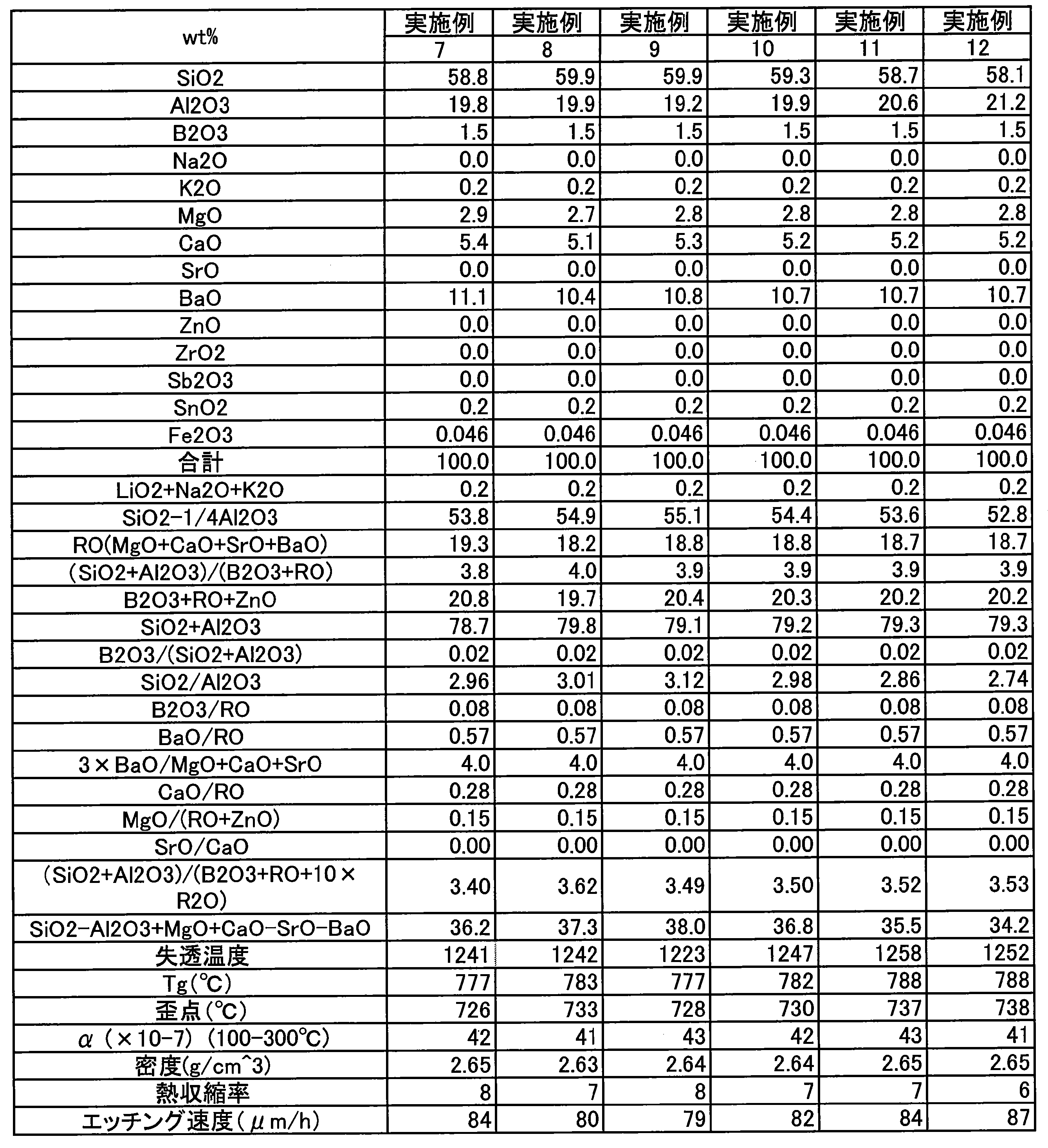
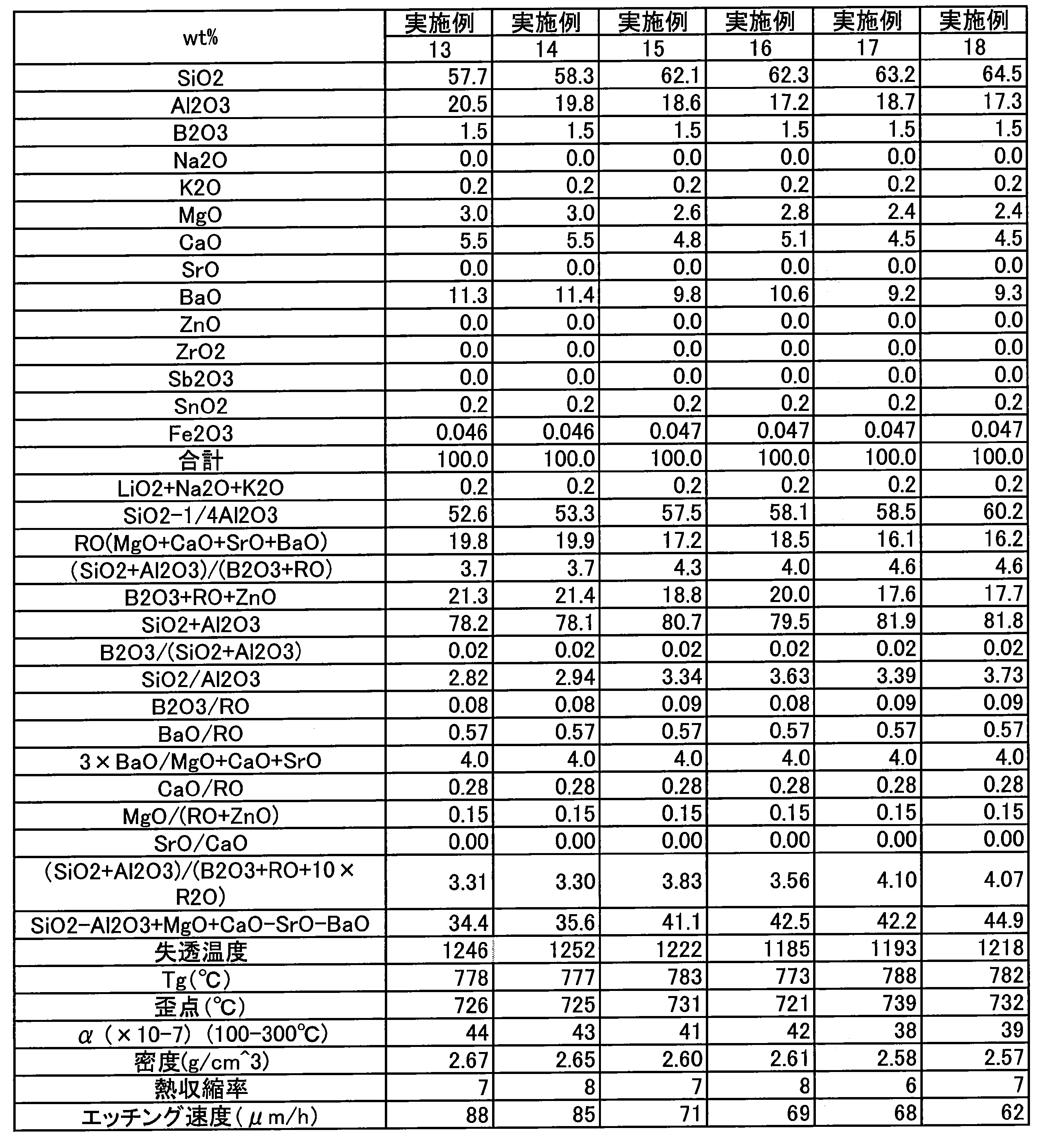


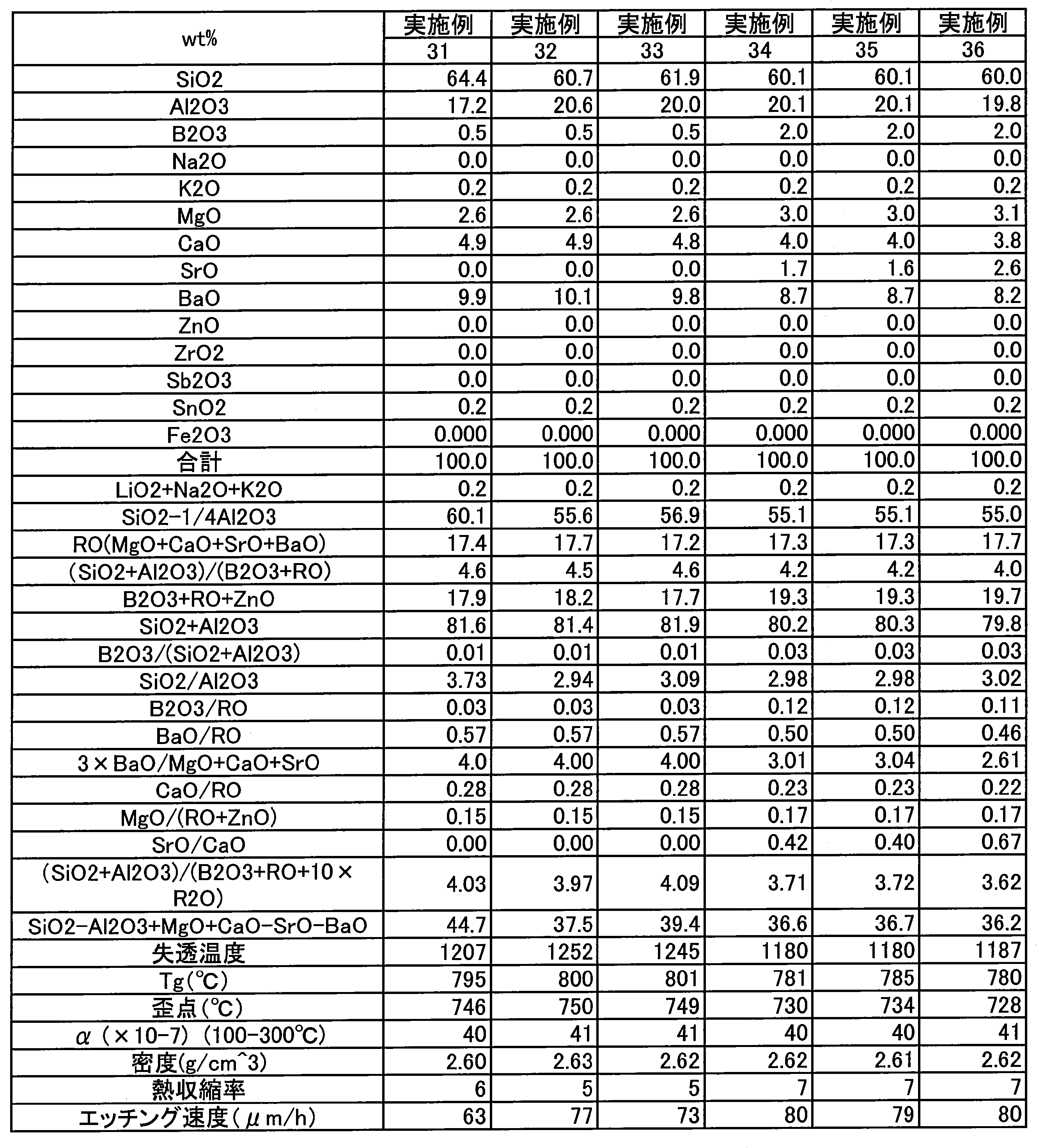


Claims (6)
- SiO2、Al2O3を含有し、
質量%表示で、
B2O3が0%以上、3%未満であり、
BaOが5~14%であり、
Sb2O3を実質的に含有せず、
失透温度が1235℃以下であり、かつ
歪点が720℃以上である、ガラスからなる、ディスプレイ用ガラス基板。 - SiO2、Al2O3を含有し、
質量%表示で、
B2O3が0%以上、3%未満であり、
MgOが1.8%以上であり、
BaOが5~14%であり、
Sb2O3を実質的に含有せず、
(SiO2+MgO+CaO)-(Al2O3+SrO+BaO)が42%未満であり、
失透温度が1260℃以下であり、かつ
歪点が720℃以上である、ガラスからなる、ディスプレイ用ガラス基板。 - 前記ガラス基板は500℃の温度で30分間保持し、その後、常温まで放冷した場合の下記式で示される熱収縮率が15ppm以下である、請求項1~2のいずれか1項に記載のガラス基板。
熱収縮率(ppm)={熱処理前後のガラスの収縮量/熱処理前のガラスの長さ}×106 - 前記ガラス基板は、エッチングレートが75μm/hより大きい、請求項1~3のいずれか1項に記載のガラス基板。
- 低温ポリシリコンまたは酸化物半導体を用いて形成された薄膜トランジスタがガラス基板表面に形成されたフラットパネルディスプレイ用ガラス基板である、請求項1~4のいずれかに記載のガラス基板。
- 所定の組成に調合したガラス原料を少なくとも直接通電加熱を用いて熔解する熔解工程と、
前記熔解工程にて熔解した熔融ガラスを平板状ガラスに成形する成形工程と、
前記平板状ガラスを徐冷する工程であって、前記平板状ガラスの熱収縮率を低減するように前記平板状ガラスの冷却条件を制御する徐冷工程と、を含む請求項1~5のいずれか1項に記載のガラス基板を製造するディスプレイ用ガラス基板の製造方法。
Priority Applications (5)
| Application Number | Priority Date | Filing Date | Title |
|---|---|---|---|
| CN201680037857.8A CN107735376A (zh) | 2015-06-30 | 2016-06-28 | 显示器用玻璃基板及其制造方法 |
| US15/740,906 US11069716B2 (en) | 2015-06-30 | 2016-06-28 | Glass substrate for display and method for producing same |
| KR1020187002478A KR102295451B1 (ko) | 2015-06-30 | 2016-06-28 | 디스플레이용 유리 기판 및 그 제조 방법 |
| JP2017526371A JP6692812B2 (ja) | 2015-06-30 | 2016-06-28 | ディスプレイ用ガラス基板およびその製造方法 |
| CN201810967486.4A CN109133615B (zh) | 2015-06-30 | 2016-06-28 | 显示器用玻璃基板及其制造方法 |
Applications Claiming Priority (2)
| Application Number | Priority Date | Filing Date | Title |
|---|---|---|---|
| JP2015-131780 | 2015-06-30 | ||
| JP2015131780 | 2015-06-30 |
Publications (1)
| Publication Number | Publication Date |
|---|---|
| WO2017002808A1 true WO2017002808A1 (ja) | 2017-01-05 |
Family
ID=57609393
Family Applications (1)
| Application Number | Title | Priority Date | Filing Date |
|---|---|---|---|
| PCT/JP2016/069145 WO2017002808A1 (ja) | 2015-06-30 | 2016-06-28 | ディスプレイ用ガラス基板およびその製造方法 |
Country Status (6)
| Country | Link |
|---|---|
| US (1) | US11069716B2 (ja) |
| JP (1) | JP6692812B2 (ja) |
| KR (1) | KR102295451B1 (ja) |
| CN (2) | CN109133615B (ja) |
| TW (1) | TWI687382B (ja) |
| WO (1) | WO2017002808A1 (ja) |
Cited By (6)
| Publication number | Priority date | Publication date | Assignee | Title |
|---|---|---|---|---|
| JP2019131429A (ja) * | 2018-01-31 | 2019-08-08 | 日本電気硝子株式会社 | ガラス |
| JPWO2018123675A1 (ja) * | 2016-12-28 | 2019-10-31 | 日本電気硝子株式会社 | ガラス |
| KR20200016964A (ko) * | 2017-06-30 | 2020-02-17 | 퉁수 테크놀로지 그룹 컴퍼니 리미티드 | 알루미노보로실리케이트 유리 및 그 제조방법 및 그 적용 |
| JP2022009065A (ja) * | 2017-03-22 | 2022-01-14 | 日本電気硝子株式会社 | ガラス板及びその製造方法 |
| WO2023084979A1 (ja) * | 2021-11-10 | 2023-05-19 | 日本電気硝子株式会社 | 無アルカリガラス板 |
| JP7478340B2 (ja) | 2018-10-17 | 2024-05-07 | 日本電気硝子株式会社 | 無アルカリガラス板 |
Families Citing this family (4)
| Publication number | Priority date | Publication date | Assignee | Title |
|---|---|---|---|---|
| CN107709257A (zh) * | 2015-06-30 | 2018-02-16 | 安瀚视特控股株式会社 | 显示器用玻璃基板及其制造方法 |
| CN110357420B (zh) * | 2019-07-23 | 2022-03-04 | 中国洛阳浮法玻璃集团有限责任公司 | 一种低热收缩率电子基板玻璃的制备方法 |
| JPWO2021261446A1 (ja) * | 2020-06-25 | 2021-12-30 | ||
| CN112557435A (zh) * | 2020-12-08 | 2021-03-26 | 河北光兴半导体技术有限公司 | 玻璃热收缩率测定系统、方法、存储介质和电子设备 |
Citations (7)
| Publication number | Priority date | Publication date | Assignee | Title |
|---|---|---|---|---|
| JPH04175242A (ja) * | 1990-11-06 | 1992-06-23 | Asahi Glass Co Ltd | 無アルカリガラス |
| JP2009525942A (ja) * | 2006-02-10 | 2009-07-16 | コーニング インコーポレイテッド | 熱および化学安定性が高いガラス組成物ならびにその製造方法 |
| WO2012063643A1 (ja) * | 2010-11-08 | 2012-05-18 | 日本電気硝子株式会社 | 無アルカリガラス |
| WO2012108345A1 (ja) * | 2011-02-08 | 2012-08-16 | 旭硝子株式会社 | ガラス組成物およびガラス組成物を用いた太陽電池用ガラス基板、並びにディスプレイパネル用ガラス基板 |
| JP2012184146A (ja) * | 2011-03-08 | 2012-09-27 | Nippon Electric Glass Co Ltd | 無アルカリガラス |
| JP2015071523A (ja) * | 2012-12-28 | 2015-04-16 | AvanStrate株式会社 | ディスプレイ用ガラス基板およびその製造方法 |
| JP2015512849A (ja) * | 2012-02-28 | 2015-04-30 | コーニング インコーポレイテッド | 高歪点アルミノシリケートガラス |
Family Cites Families (19)
| Publication number | Priority date | Publication date | Assignee | Title |
|---|---|---|---|---|
| JP2004315354A (ja) | 2003-03-31 | 2004-11-11 | Asahi Glass Co Ltd | 無アルカリガラス |
| US7727917B2 (en) * | 2003-10-24 | 2010-06-01 | Schott Ag | Lithia-alumina-silica containing glass compositions and glasses suitable for chemical tempering and articles made using the chemically tempered glass |
| CN101522584B (zh) * | 2006-10-10 | 2012-12-05 | 日本电气硝子株式会社 | 钢化玻璃基板 |
| JP5483821B2 (ja) * | 2007-02-27 | 2014-05-07 | AvanStrate株式会社 | 表示装置用ガラス基板および表示装置 |
| JP5435394B2 (ja) * | 2007-06-08 | 2014-03-05 | 日本電気硝子株式会社 | 強化ガラス基板及びその製造方法 |
| JP5467490B2 (ja) * | 2007-08-03 | 2014-04-09 | 日本電気硝子株式会社 | 強化ガラス基板の製造方法及び強化ガラス基板 |
| JP5573157B2 (ja) * | 2007-10-25 | 2014-08-20 | 旭硝子株式会社 | 基板用ガラス組成物および板ガラスの製造方法 |
| US8187715B2 (en) * | 2008-05-13 | 2012-05-29 | Corning Incorporated | Rare-earth-containing glass material and substrate and device comprising such substrate |
| JP5333984B2 (ja) | 2008-06-27 | 2013-11-06 | 日本電気硝子株式会社 | 無アルカリガラス |
| JP5622069B2 (ja) * | 2009-01-21 | 2014-11-12 | 日本電気硝子株式会社 | 強化ガラス、強化用ガラス及び強化ガラスの製造方法 |
| JP5537144B2 (ja) | 2009-12-16 | 2014-07-02 | AvanStrate株式会社 | ガラス組成物とそれを用いたフラットパネルディスプレイ用ガラス基板 |
| JP5874316B2 (ja) | 2010-10-27 | 2016-03-02 | 日本電気硝子株式会社 | 無アルカリガラス |
| JP5172045B2 (ja) * | 2011-07-01 | 2013-03-27 | AvanStrate株式会社 | フラットパネルディスプレイ用ガラス基板及びその製造方法 |
| IN2014DN07444A (ja) | 2012-02-29 | 2015-04-24 | Corning Inc | |
| CN104125935A (zh) * | 2012-06-08 | 2014-10-29 | 日本电气硝子株式会社 | 强化玻璃、强化玻璃板以及强化用玻璃 |
| JP6037117B2 (ja) * | 2012-12-14 | 2016-11-30 | 日本電気硝子株式会社 | ガラス及びガラス基板 |
| JP2017007870A (ja) | 2013-11-13 | 2017-01-12 | 旭硝子株式会社 | 板ガラスの製造方法 |
| CN107406303A (zh) * | 2015-06-02 | 2017-11-28 | 日本电气硝子株式会社 | 玻璃 |
| CN107709257A (zh) * | 2015-06-30 | 2018-02-16 | 安瀚视特控股株式会社 | 显示器用玻璃基板及其制造方法 |
-
2016
- 2016-06-28 CN CN201810967486.4A patent/CN109133615B/zh active Active
- 2016-06-28 JP JP2017526371A patent/JP6692812B2/ja active Active
- 2016-06-28 KR KR1020187002478A patent/KR102295451B1/ko active IP Right Grant
- 2016-06-28 WO PCT/JP2016/069145 patent/WO2017002808A1/ja active Application Filing
- 2016-06-28 CN CN201680037857.8A patent/CN107735376A/zh active Pending
- 2016-06-28 US US15/740,906 patent/US11069716B2/en active Active
- 2016-06-30 TW TW105120827A patent/TWI687382B/zh active
Patent Citations (7)
| Publication number | Priority date | Publication date | Assignee | Title |
|---|---|---|---|---|
| JPH04175242A (ja) * | 1990-11-06 | 1992-06-23 | Asahi Glass Co Ltd | 無アルカリガラス |
| JP2009525942A (ja) * | 2006-02-10 | 2009-07-16 | コーニング インコーポレイテッド | 熱および化学安定性が高いガラス組成物ならびにその製造方法 |
| WO2012063643A1 (ja) * | 2010-11-08 | 2012-05-18 | 日本電気硝子株式会社 | 無アルカリガラス |
| WO2012108345A1 (ja) * | 2011-02-08 | 2012-08-16 | 旭硝子株式会社 | ガラス組成物およびガラス組成物を用いた太陽電池用ガラス基板、並びにディスプレイパネル用ガラス基板 |
| JP2012184146A (ja) * | 2011-03-08 | 2012-09-27 | Nippon Electric Glass Co Ltd | 無アルカリガラス |
| JP2015512849A (ja) * | 2012-02-28 | 2015-04-30 | コーニング インコーポレイテッド | 高歪点アルミノシリケートガラス |
| JP2015071523A (ja) * | 2012-12-28 | 2015-04-16 | AvanStrate株式会社 | ディスプレイ用ガラス基板およびその製造方法 |
Cited By (11)
| Publication number | Priority date | Publication date | Assignee | Title |
|---|---|---|---|---|
| JPWO2018123675A1 (ja) * | 2016-12-28 | 2019-10-31 | 日本電気硝子株式会社 | ガラス |
| JP7121345B2 (ja) | 2016-12-28 | 2022-08-18 | 日本電気硝子株式会社 | ガラス |
| JP2022009065A (ja) * | 2017-03-22 | 2022-01-14 | 日本電気硝子株式会社 | ガラス板及びその製造方法 |
| US11753329B2 (en) | 2017-03-22 | 2023-09-12 | Nippon Electric Glass Co., Ltd. | Glass plate and method for manufacturing same |
| JP7382014B2 (ja) | 2017-03-22 | 2023-11-16 | 日本電気硝子株式会社 | ガラス板及びその製造方法 |
| KR20200016964A (ko) * | 2017-06-30 | 2020-02-17 | 퉁수 테크놀로지 그룹 컴퍼니 리미티드 | 알루미노보로실리케이트 유리 및 그 제조방법 및 그 적용 |
| KR102292470B1 (ko) | 2017-06-30 | 2021-08-23 | 퉁수 테크놀로지 그룹 컴퍼니 리미티드 | 알루미노보로실리케이트 유리 및 그 제조방법 및 그 적용 |
| JP2019131429A (ja) * | 2018-01-31 | 2019-08-08 | 日本電気硝子株式会社 | ガラス |
| JP7418947B2 (ja) | 2018-01-31 | 2024-01-22 | 日本電気硝子株式会社 | ガラス |
| JP7478340B2 (ja) | 2018-10-17 | 2024-05-07 | 日本電気硝子株式会社 | 無アルカリガラス板 |
| WO2023084979A1 (ja) * | 2021-11-10 | 2023-05-19 | 日本電気硝子株式会社 | 無アルカリガラス板 |
Also Published As
| Publication number | Publication date |
|---|---|
| CN109133615A (zh) | 2019-01-04 |
| CN109133615B (zh) | 2022-05-10 |
| TWI687382B (zh) | 2020-03-11 |
| US11069716B2 (en) | 2021-07-20 |
| CN107735376A (zh) | 2018-02-23 |
| KR20180022872A (ko) | 2018-03-06 |
| KR102295451B1 (ko) | 2021-08-27 |
| JP6692812B2 (ja) | 2020-05-13 |
| JPWO2017002808A1 (ja) | 2018-04-12 |
| TW201706223A (zh) | 2017-02-16 |
| US20180190675A1 (en) | 2018-07-05 |
Similar Documents
| Publication | Publication Date | Title |
|---|---|---|
| JP6375277B2 (ja) | ディスプレイ用ガラス基板およびその製造方法 | |
| JP6692812B2 (ja) | ディスプレイ用ガラス基板およびその製造方法 | |
| JP6105539B2 (ja) | フラットパネルディスプレイ用ガラス基板およびその製造方法 | |
| KR101351112B1 (ko) | 플랫 패널 디스플레이용 유리 기판 및 그 제조 방법 | |
| JP2017071548A (ja) | フラットパネルディスプレイ用ガラス基板及びその製造方法 | |
| JP6867946B2 (ja) | ディスプレイ用ガラス基板およびその製造方法 | |
| JP6587969B2 (ja) | 磁気記録媒体用ガラス基板およびその製造方法 | |
| JP5753895B2 (ja) | フラットパネルディスプレイ用ガラス基板 | |
| JP7140582B2 (ja) | ディスプレイ用ガラス基板 |
Legal Events
| Date | Code | Title | Description |
|---|---|---|---|
| 121 | Ep: the epo has been informed by wipo that ep was designated in this application |
Ref document number: 16817916 Country of ref document: EP Kind code of ref document: A1 |
|
| ENP | Entry into the national phase |
Ref document number: 2017526371 Country of ref document: JP Kind code of ref document: A |
|
| NENP | Non-entry into the national phase |
Ref country code: DE |
|
| ENP | Entry into the national phase |
Ref document number: 20187002478 Country of ref document: KR Kind code of ref document: A |
|
| 122 | Ep: pct application non-entry in european phase |
Ref document number: 16817916 Country of ref document: EP Kind code of ref document: A1 |