WO2016194893A1 - 半導体用保護フィルム、半導体装置及び複合シート - Google Patents
半導体用保護フィルム、半導体装置及び複合シート Download PDFInfo
- Publication number
- WO2016194893A1 WO2016194893A1 PCT/JP2016/065992 JP2016065992W WO2016194893A1 WO 2016194893 A1 WO2016194893 A1 WO 2016194893A1 JP 2016065992 W JP2016065992 W JP 2016065992W WO 2016194893 A1 WO2016194893 A1 WO 2016194893A1
- Authority
- WO
- WIPO (PCT)
- Prior art keywords
- semiconductor
- layer
- protective film
- protective layer
- protective
- Prior art date
- Legal status (The legal status is an assumption and is not a legal conclusion. Google has not performed a legal analysis and makes no representation as to the accuracy of the status listed.)
- Ceased
Links
Images




Classifications
-
- H—ELECTRICITY
- H10—SEMICONDUCTOR DEVICES; ELECTRIC SOLID-STATE DEVICES NOT OTHERWISE PROVIDED FOR
- H10W—GENERIC PACKAGES, INTERCONNECTIONS, CONNECTORS OR OTHER CONSTRUCTIONAL DETAILS OF DEVICES COVERED BY CLASS H10
- H10W74/00—Encapsulations, e.g. protective coatings
- H10W74/10—Encapsulations, e.g. protective coatings characterised by their shape or disposition
-
- H—ELECTRICITY
- H10—SEMICONDUCTOR DEVICES; ELECTRIC SOLID-STATE DEVICES NOT OTHERWISE PROVIDED FOR
- H10W—GENERIC PACKAGES, INTERCONNECTIONS, CONNECTORS OR OTHER CONSTRUCTIONAL DETAILS OF DEVICES COVERED BY CLASS H10
- H10W90/00—Package configurations
-
- H—ELECTRICITY
- H10—SEMICONDUCTOR DEVICES; ELECTRIC SOLID-STATE DEVICES NOT OTHERWISE PROVIDED FOR
- H10P—GENERIC PROCESSES OR APPARATUS FOR THE MANUFACTURE OR TREATMENT OF DEVICES COVERED BY CLASS H10
- H10P72/00—Handling or holding of wafers, substrates or devices during manufacture or treatment thereof
- H10P72/70—Handling or holding of wafers, substrates or devices during manufacture or treatment thereof for supporting or gripping
- H10P72/74—Handling or holding of wafers, substrates or devices during manufacture or treatment thereof for supporting or gripping using temporarily an auxiliary support
- H10P72/7422—Handling or holding of wafers, substrates or devices during manufacture or treatment thereof for supporting or gripping using temporarily an auxiliary support used to protect an active side of a device or wafer
-
- H—ELECTRICITY
- H10—SEMICONDUCTOR DEVICES; ELECTRIC SOLID-STATE DEVICES NOT OTHERWISE PROVIDED FOR
- H10W—GENERIC PACKAGES, INTERCONNECTIONS, CONNECTORS OR OTHER CONSTRUCTIONAL DETAILS OF DEVICES COVERED BY CLASS H10
- H10W42/00—Arrangements for protection of devices
- H10W42/121—Arrangements for protection of devices protecting against mechanical damage
-
- H—ELECTRICITY
- H10—SEMICONDUCTOR DEVICES; ELECTRIC SOLID-STATE DEVICES NOT OTHERWISE PROVIDED FOR
- H10W—GENERIC PACKAGES, INTERCONNECTIONS, CONNECTORS OR OTHER CONSTRUCTIONAL DETAILS OF DEVICES COVERED BY CLASS H10
- H10W74/00—Encapsulations, e.g. protective coatings
- H10W74/01—Manufacture or treatment
- H10W74/012—Manufacture or treatment of encapsulations on active surfaces of flip-chip devices, e.g. forming underfills
-
- H—ELECTRICITY
- H10—SEMICONDUCTOR DEVICES; ELECTRIC SOLID-STATE DEVICES NOT OTHERWISE PROVIDED FOR
- H10P—GENERIC PROCESSES OR APPARATUS FOR THE MANUFACTURE OR TREATMENT OF DEVICES COVERED BY CLASS H10
- H10P54/00—Cutting or separating of wafers, substrates or parts of devices
-
- H—ELECTRICITY
- H10—SEMICONDUCTOR DEVICES; ELECTRIC SOLID-STATE DEVICES NOT OTHERWISE PROVIDED FOR
- H10P—GENERIC PROCESSES OR APPARATUS FOR THE MANUFACTURE OR TREATMENT OF DEVICES COVERED BY CLASS H10
- H10P72/00—Handling or holding of wafers, substrates or devices during manufacture or treatment thereof
- H10P72/70—Handling or holding of wafers, substrates or devices during manufacture or treatment thereof for supporting or gripping
- H10P72/74—Handling or holding of wafers, substrates or devices during manufacture or treatment thereof for supporting or gripping using temporarily an auxiliary support
- H10P72/7402—Wafer tapes, e.g. grinding or dicing support tapes
-
- H—ELECTRICITY
- H10—SEMICONDUCTOR DEVICES; ELECTRIC SOLID-STATE DEVICES NOT OTHERWISE PROVIDED FOR
- H10P—GENERIC PROCESSES OR APPARATUS FOR THE MANUFACTURE OR TREATMENT OF DEVICES COVERED BY CLASS H10
- H10P72/00—Handling or holding of wafers, substrates or devices during manufacture or treatment thereof
- H10P72/70—Handling or holding of wafers, substrates or devices during manufacture or treatment thereof for supporting or gripping
- H10P72/74—Handling or holding of wafers, substrates or devices during manufacture or treatment thereof for supporting or gripping using temporarily an auxiliary support
- H10P72/7416—Handling or holding of wafers, substrates or devices during manufacture or treatment thereof for supporting or gripping using temporarily an auxiliary support used during dicing or grinding
-
- H—ELECTRICITY
- H10—SEMICONDUCTOR DEVICES; ELECTRIC SOLID-STATE DEVICES NOT OTHERWISE PROVIDED FOR
- H10W—GENERIC PACKAGES, INTERCONNECTIONS, CONNECTORS OR OTHER CONSTRUCTIONAL DETAILS OF DEVICES COVERED BY CLASS H10
- H10W46/00—Marks applied to devices, e.g. for alignment or identification
-
- H—ELECTRICITY
- H10—SEMICONDUCTOR DEVICES; ELECTRIC SOLID-STATE DEVICES NOT OTHERWISE PROVIDED FOR
- H10W—GENERIC PACKAGES, INTERCONNECTIONS, CONNECTORS OR OTHER CONSTRUCTIONAL DETAILS OF DEVICES COVERED BY CLASS H10
- H10W46/00—Marks applied to devices, e.g. for alignment or identification
- H10W46/401—Marks applied to devices, e.g. for alignment or identification for identification or tracking
-
- H—ELECTRICITY
- H10—SEMICONDUCTOR DEVICES; ELECTRIC SOLID-STATE DEVICES NOT OTHERWISE PROVIDED FOR
- H10W—GENERIC PACKAGES, INTERCONNECTIONS, CONNECTORS OR OTHER CONSTRUCTIONAL DETAILS OF DEVICES COVERED BY CLASS H10
- H10W46/00—Marks applied to devices, e.g. for alignment or identification
- H10W46/601—Marks applied to devices, e.g. for alignment or identification for use after dicing
- H10W46/607—Located on parts of packages, e.g. on encapsulations or on package substrates
-
- H—ELECTRICITY
- H10—SEMICONDUCTOR DEVICES; ELECTRIC SOLID-STATE DEVICES NOT OTHERWISE PROVIDED FOR
- H10W—GENERIC PACKAGES, INTERCONNECTIONS, CONNECTORS OR OTHER CONSTRUCTIONAL DETAILS OF DEVICES COVERED BY CLASS H10
- H10W70/00—Package substrates; Interposers; Redistribution layers [RDL]
- H10W70/60—Insulating or insulated package substrates; Interposers; Redistribution layers
-
- H—ELECTRICITY
- H10—SEMICONDUCTOR DEVICES; ELECTRIC SOLID-STATE DEVICES NOT OTHERWISE PROVIDED FOR
- H10W—GENERIC PACKAGES, INTERCONNECTIONS, CONNECTORS OR OTHER CONSTRUCTIONAL DETAILS OF DEVICES COVERED BY CLASS H10
- H10W70/00—Package substrates; Interposers; Redistribution layers [RDL]
- H10W70/60—Insulating or insulated package substrates; Interposers; Redistribution layers
- H10W70/62—Insulating or insulated package substrates; Interposers; Redistribution layers characterised by their interconnections
- H10W70/63—Vias, e.g. via plugs
- H10W70/635—Through-vias
-
- H—ELECTRICITY
- H10—SEMICONDUCTOR DEVICES; ELECTRIC SOLID-STATE DEVICES NOT OTHERWISE PROVIDED FOR
- H10W—GENERIC PACKAGES, INTERCONNECTIONS, CONNECTORS OR OTHER CONSTRUCTIONAL DETAILS OF DEVICES COVERED BY CLASS H10
- H10W72/00—Interconnections or connectors in packages
- H10W72/01—Manufacture or treatment
- H10W72/013—Manufacture or treatment of die-attach connectors
-
- H—ELECTRICITY
- H10—SEMICONDUCTOR DEVICES; ELECTRIC SOLID-STATE DEVICES NOT OTHERWISE PROVIDED FOR
- H10W—GENERIC PACKAGES, INTERCONNECTIONS, CONNECTORS OR OTHER CONSTRUCTIONAL DETAILS OF DEVICES COVERED BY CLASS H10
- H10W72/00—Interconnections or connectors in packages
- H10W72/01—Manufacture or treatment
- H10W72/0198—Manufacture or treatment batch processes
-
- H—ELECTRICITY
- H10—SEMICONDUCTOR DEVICES; ELECTRIC SOLID-STATE DEVICES NOT OTHERWISE PROVIDED FOR
- H10W—GENERIC PACKAGES, INTERCONNECTIONS, CONNECTORS OR OTHER CONSTRUCTIONAL DETAILS OF DEVICES COVERED BY CLASS H10
- H10W72/00—Interconnections or connectors in packages
- H10W72/30—Die-attach connectors
- H10W72/321—Structures or relative sizes of die-attach connectors
- H10W72/322—Multilayered die-attach connectors, e.g. a coating on a top surface of a core
-
- H—ELECTRICITY
- H10—SEMICONDUCTOR DEVICES; ELECTRIC SOLID-STATE DEVICES NOT OTHERWISE PROVIDED FOR
- H10W—GENERIC PACKAGES, INTERCONNECTIONS, CONNECTORS OR OTHER CONSTRUCTIONAL DETAILS OF DEVICES COVERED BY CLASS H10
- H10W72/00—Interconnections or connectors in packages
- H10W72/30—Die-attach connectors
- H10W72/321—Structures or relative sizes of die-attach connectors
- H10W72/325—Die-attach connectors having a filler embedded in a matrix
-
- H—ELECTRICITY
- H10—SEMICONDUCTOR DEVICES; ELECTRIC SOLID-STATE DEVICES NOT OTHERWISE PROVIDED FOR
- H10W—GENERIC PACKAGES, INTERCONNECTIONS, CONNECTORS OR OTHER CONSTRUCTIONAL DETAILS OF DEVICES COVERED BY CLASS H10
- H10W72/00—Interconnections or connectors in packages
- H10W72/30—Die-attach connectors
- H10W72/351—Materials of die-attach connectors
- H10W72/353—Materials of die-attach connectors not comprising solid metals or solid metalloids, e.g. ceramics
-
- H—ELECTRICITY
- H10—SEMICONDUCTOR DEVICES; ELECTRIC SOLID-STATE DEVICES NOT OTHERWISE PROVIDED FOR
- H10W—GENERIC PACKAGES, INTERCONNECTIONS, CONNECTORS OR OTHER CONSTRUCTIONAL DETAILS OF DEVICES COVERED BY CLASS H10
- H10W72/00—Interconnections or connectors in packages
- H10W72/30—Die-attach connectors
- H10W72/351—Materials of die-attach connectors
- H10W72/353—Materials of die-attach connectors not comprising solid metals or solid metalloids, e.g. ceramics
- H10W72/354—Materials of die-attach connectors not comprising solid metals or solid metalloids, e.g. ceramics comprising polymers
-
- H—ELECTRICITY
- H10—SEMICONDUCTOR DEVICES; ELECTRIC SOLID-STATE DEVICES NOT OTHERWISE PROVIDED FOR
- H10W—GENERIC PACKAGES, INTERCONNECTIONS, CONNECTORS OR OTHER CONSTRUCTIONAL DETAILS OF DEVICES COVERED BY CLASS H10
- H10W72/00—Interconnections or connectors in packages
- H10W72/50—Bond wires
- H10W72/541—Dispositions of bond wires
- H10W72/5445—Dispositions of bond wires being orthogonal to a side surface of the chip, e.g. parallel arrangements
-
- H—ELECTRICITY
- H10—SEMICONDUCTOR DEVICES; ELECTRIC SOLID-STATE DEVICES NOT OTHERWISE PROVIDED FOR
- H10W—GENERIC PACKAGES, INTERCONNECTIONS, CONNECTORS OR OTHER CONSTRUCTIONAL DETAILS OF DEVICES COVERED BY CLASS H10
- H10W72/00—Interconnections or connectors in packages
- H10W72/823—Interconnections through encapsulations, e.g. pillars through molded resin on a lateral side a chip
-
- H—ELECTRICITY
- H10—SEMICONDUCTOR DEVICES; ELECTRIC SOLID-STATE DEVICES NOT OTHERWISE PROVIDED FOR
- H10W—GENERIC PACKAGES, INTERCONNECTIONS, CONNECTORS OR OTHER CONSTRUCTIONAL DETAILS OF DEVICES COVERED BY CLASS H10
- H10W72/00—Interconnections or connectors in packages
- H10W72/851—Dispositions of multiple connectors or interconnections
- H10W72/874—On different surfaces
- H10W72/877—Bump connectors and die-attach connectors
-
- H—ELECTRICITY
- H10—SEMICONDUCTOR DEVICES; ELECTRIC SOLID-STATE DEVICES NOT OTHERWISE PROVIDED FOR
- H10W—GENERIC PACKAGES, INTERCONNECTIONS, CONNECTORS OR OTHER CONSTRUCTIONAL DETAILS OF DEVICES COVERED BY CLASS H10
- H10W72/00—Interconnections or connectors in packages
- H10W72/851—Dispositions of multiple connectors or interconnections
- H10W72/874—On different surfaces
- H10W72/884—Die-attach connectors and bond wires
-
- H—ELECTRICITY
- H10—SEMICONDUCTOR DEVICES; ELECTRIC SOLID-STATE DEVICES NOT OTHERWISE PROVIDED FOR
- H10W—GENERIC PACKAGES, INTERCONNECTIONS, CONNECTORS OR OTHER CONSTRUCTIONAL DETAILS OF DEVICES COVERED BY CLASS H10
- H10W74/00—Encapsulations, e.g. protective coatings
-
- H—ELECTRICITY
- H10—SEMICONDUCTOR DEVICES; ELECTRIC SOLID-STATE DEVICES NOT OTHERWISE PROVIDED FOR
- H10W—GENERIC PACKAGES, INTERCONNECTIONS, CONNECTORS OR OTHER CONSTRUCTIONAL DETAILS OF DEVICES COVERED BY CLASS H10
- H10W74/00—Encapsulations, e.g. protective coatings
- H10W74/10—Encapsulations, e.g. protective coatings characterised by their shape or disposition
- H10W74/111—Encapsulations, e.g. protective coatings characterised by their shape or disposition the semiconductor body being completely enclosed
- H10W74/114—Encapsulations, e.g. protective coatings characterised by their shape or disposition the semiconductor body being completely enclosed by a substrate and the encapsulations
- H10W74/117—Encapsulations, e.g. protective coatings characterised by their shape or disposition the semiconductor body being completely enclosed by a substrate and the encapsulations the substrate having spherical bumps for external connection
-
- H—ELECTRICITY
- H10—SEMICONDUCTOR DEVICES; ELECTRIC SOLID-STATE DEVICES NOT OTHERWISE PROVIDED FOR
- H10W—GENERIC PACKAGES, INTERCONNECTIONS, CONNECTORS OR OTHER CONSTRUCTIONAL DETAILS OF DEVICES COVERED BY CLASS H10
- H10W74/00—Encapsulations, e.g. protective coatings
- H10W74/10—Encapsulations, e.g. protective coatings characterised by their shape or disposition
- H10W74/15—Encapsulations, e.g. protective coatings characterised by their shape or disposition on active surfaces of flip-chip devices, e.g. underfills
-
- H—ELECTRICITY
- H10—SEMICONDUCTOR DEVICES; ELECTRIC SOLID-STATE DEVICES NOT OTHERWISE PROVIDED FOR
- H10W—GENERIC PACKAGES, INTERCONNECTIONS, CONNECTORS OR OTHER CONSTRUCTIONAL DETAILS OF DEVICES COVERED BY CLASS H10
- H10W90/00—Package configurations
- H10W90/20—Configurations of stacked chips
- H10W90/24—Configurations of stacked chips at least one of the stacked chips being laterally offset from a neighbouring stacked chip, e.g. chip stacks having a staircase shape
-
- H—ELECTRICITY
- H10—SEMICONDUCTOR DEVICES; ELECTRIC SOLID-STATE DEVICES NOT OTHERWISE PROVIDED FOR
- H10W—GENERIC PACKAGES, INTERCONNECTIONS, CONNECTORS OR OTHER CONSTRUCTIONAL DETAILS OF DEVICES COVERED BY CLASS H10
- H10W90/00—Package configurations
- H10W90/20—Configurations of stacked chips
- H10W90/28—Configurations of stacked chips the stacked chips having different sizes, e.g. chip stacks having a pyramidal shape
-
- H—ELECTRICITY
- H10—SEMICONDUCTOR DEVICES; ELECTRIC SOLID-STATE DEVICES NOT OTHERWISE PROVIDED FOR
- H10W—GENERIC PACKAGES, INTERCONNECTIONS, CONNECTORS OR OTHER CONSTRUCTIONAL DETAILS OF DEVICES COVERED BY CLASS H10
- H10W90/00—Package configurations
- H10W90/20—Configurations of stacked chips
- H10W90/291—Configurations of stacked chips characterised by containers, encapsulations, or other housings for the stacked chips
-
- H—ELECTRICITY
- H10—SEMICONDUCTOR DEVICES; ELECTRIC SOLID-STATE DEVICES NOT OTHERWISE PROVIDED FOR
- H10W—GENERIC PACKAGES, INTERCONNECTIONS, CONNECTORS OR OTHER CONSTRUCTIONAL DETAILS OF DEVICES COVERED BY CLASS H10
- H10W90/00—Package configurations
- H10W90/701—Package configurations characterised by the relative positions of pads or connectors relative to package parts
- H10W90/721—Package configurations characterised by the relative positions of pads or connectors relative to package parts of bump connectors
- H10W90/722—Package configurations characterised by the relative positions of pads or connectors relative to package parts of bump connectors between stacked chips
-
- H—ELECTRICITY
- H10—SEMICONDUCTOR DEVICES; ELECTRIC SOLID-STATE DEVICES NOT OTHERWISE PROVIDED FOR
- H10W—GENERIC PACKAGES, INTERCONNECTIONS, CONNECTORS OR OTHER CONSTRUCTIONAL DETAILS OF DEVICES COVERED BY CLASS H10
- H10W90/00—Package configurations
- H10W90/701—Package configurations characterised by the relative positions of pads or connectors relative to package parts
- H10W90/721—Package configurations characterised by the relative positions of pads or connectors relative to package parts of bump connectors
- H10W90/724—Package configurations characterised by the relative positions of pads or connectors relative to package parts of bump connectors between a chip and a stacked insulating package substrate, interposer or RDL
-
- H—ELECTRICITY
- H10—SEMICONDUCTOR DEVICES; ELECTRIC SOLID-STATE DEVICES NOT OTHERWISE PROVIDED FOR
- H10W—GENERIC PACKAGES, INTERCONNECTIONS, CONNECTORS OR OTHER CONSTRUCTIONAL DETAILS OF DEVICES COVERED BY CLASS H10
- H10W90/00—Package configurations
- H10W90/701—Package configurations characterised by the relative positions of pads or connectors relative to package parts
- H10W90/731—Package configurations characterised by the relative positions of pads or connectors relative to package parts of die-attach connectors
- H10W90/732—Package configurations characterised by the relative positions of pads or connectors relative to package parts of die-attach connectors between stacked chips
-
- H—ELECTRICITY
- H10—SEMICONDUCTOR DEVICES; ELECTRIC SOLID-STATE DEVICES NOT OTHERWISE PROVIDED FOR
- H10W—GENERIC PACKAGES, INTERCONNECTIONS, CONNECTORS OR OTHER CONSTRUCTIONAL DETAILS OF DEVICES COVERED BY CLASS H10
- H10W90/00—Package configurations
- H10W90/701—Package configurations characterised by the relative positions of pads or connectors relative to package parts
- H10W90/731—Package configurations characterised by the relative positions of pads or connectors relative to package parts of die-attach connectors
- H10W90/734—Package configurations characterised by the relative positions of pads or connectors relative to package parts of die-attach connectors between a chip and a stacked insulating package substrate, interposer or RDL
-
- H—ELECTRICITY
- H10—SEMICONDUCTOR DEVICES; ELECTRIC SOLID-STATE DEVICES NOT OTHERWISE PROVIDED FOR
- H10W—GENERIC PACKAGES, INTERCONNECTIONS, CONNECTORS OR OTHER CONSTRUCTIONAL DETAILS OF DEVICES COVERED BY CLASS H10
- H10W90/00—Package configurations
- H10W90/701—Package configurations characterised by the relative positions of pads or connectors relative to package parts
- H10W90/751—Package configurations characterised by the relative positions of pads or connectors relative to package parts of bond wires
- H10W90/754—Package configurations characterised by the relative positions of pads or connectors relative to package parts of bond wires between a chip and a stacked insulating package substrate, interposer or RDL
Definitions
- the present invention relates to a protective film for a semiconductor that is adhered to the back surface of a semiconductor element such as a semiconductor chip, a semiconductor device including the same, and a composite sheet.
- the surface (active surface) constituting the circuit surface of the semiconductor chip is arranged to face the wiring substrate, and is formed on the wiring substrate via a plurality of electrodes called bumps formed on the surface of the semiconductor chip. Connected electrically and mechanically.
- a protective film is often attached to the back surface (inactive surface) of a semiconductor chip mounted in a face-down manner for the purpose of protecting the semiconductor chip.
- a flip chip type semiconductor back film comprising an adhesive layer and a protective layer laminated on the adhesive layer, wherein the protective layer is made of a heat resistant resin or metal. It is known (see, for example, Patent Document 1).
- Patent Document 1 in the adhesive layer of the protective film attached to the back surface of the semiconductor chip, the warping of the package is suppressed by making the content of the thermosetting resin with respect to all the resin components below a predetermined value.
- Patent Document 1 has been proposed (paragraph [0034] of Patent Document 1).
- the rigidity or elastic modulus of the adhesive layer made of synthetic resin is relatively low, so that the warp of the semiconductor chip cannot be sufficiently suppressed.
- a relatively high elastic modulus can be ensured by forming the protective layer from a metal.
- productivity decreases, such as a reduction in processing accuracy during dicing, abrasion of the dicing saw (blade), short circuit failure of the semiconductor chip circuit surface due to chip adhesion, etc. It causes various problems in terms of reliability.
- visibility cannot be secured.
- an object of the present invention is to provide a semiconductor protective film capable of suppressing warpage of a semiconductor chip and further ensuring visibility without impairing productivity and reliability.
- An object of the present invention is to provide a semiconductor device and a composite sheet.
- a protective film for a semiconductor includes a protective layer and an adhesive layer.
- the protective layer is made of a nonconductive inorganic material.
- the adhesive layer is provided on one surface of the protective layer.
- the semiconductor protective film can increase the elastic modulus of the protective layer as compared with the case where the protective layer is made of a synthetic resin. Thereby, it is possible to effectively suppress warping of the semiconductor element to be protected.
- the protective layer is made of a non-conductive inorganic material, compared to the case where the protective layer is made of metal, the processing accuracy during dicing is improved and the wear and deterioration of the dicing saw are suppressed. can do. Moreover, even if chips adhere to the circuit surface of the semiconductor chip, no short circuit failure occurs. As a result, productivity and reliability can be improved.
- the nonconductive inorganic material constituting the protective layer is not particularly limited, and typically includes a vitreous material, a ceramic material, or a mixture thereof.
- Typical examples of the glassy material include plate glass and glass fiber.
- the structure of the glass used for plate glass or glass fiber may be either amorphous or crystalline.
- a light-transmitting material such as glass for the non-conductive inorganic material, it is possible to ensure visibility even when printing on the surface of the adhesive layer with a laser or the like.
- the thickness can be, for example, 10 ⁇ m or more and 300 ⁇ m or less.
- the plate glass having such a thickness it is possible to contribute to the thinning of the semiconductor device, and the flexibility of the protective layer is enhanced, so that handling becomes easy.
- a semiconductor device includes a wiring substrate, a semiconductor element, and a protective film.
- the semiconductor element is flip-chip mounted on the wiring board.
- the protective film includes a protective layer made of a non-conductive inorganic material and an adhesive layer provided on one surface of the protective layer, and the adhesive layer is bonded to the back surface of the semiconductor element.
- the protective film is provided on the back surface of the semiconductor element, it is possible to obtain a semiconductor device with high connection reliability while suppressing warping of the semiconductor element.
- a printing layer may be provided on at least one surface of the protective layer.
- the print layer typically includes characters, symbols, graphics, and the like, and displays the type of the semiconductor element or semiconductor device in an identifiable manner.
- the printing layer is typically composed of at least a part of a protective layer or an adhesive layer, and is formed, for example, on the surface of the adhesive layer that is bonded to the protective layer.
- the print layer may be formed, for example, by scraping the surface of the protective layer by a laser processing method or the like, or may be formed by modifying the surface of the adhesive layer by laser light irradiation.
- the protective layer is made of a light-transmitting material such as plate glass or transparent ceramics, the protective layer is provided with light-transmitting properties. Therefore, a printing layer can be easily formed on the protective layer by laser printing or the like. can do.
- the protective film may have a print layer separately. In other words, the print layer may be composed of a layer different from the protective layer and the adhesive layer.
- the semiconductor device may further include a semiconductor package component electrically connected to the wiring board.
- the semiconductor element is disposed between the wiring board and the semiconductor package component.
- a semiconductor device includes a first wiring board, a first semiconductor element, a second semiconductor element, and a second wiring board.
- the first semiconductor element is flip-chip mounted on the first wiring board.
- the second wiring board is disposed between the first semiconductor element and the second semiconductor element.
- the second wiring board includes a protective layer, a wiring layer, and an adhesive layer.
- the protective layer is made of a nonconductive inorganic material.
- the wiring layer is provided on the protective layer and electrically connects the first wiring substrate and the second semiconductor element.
- the adhesive layer is provided on one surface of the protective layer and bonded to the back surface of the first semiconductor element.
- the second wiring board has a protective layer made of a non-conductive inorganic material, and is bonded to the back surface of the first semiconductor element through an adhesive layer.
- the composite sheet according to an embodiment of the present invention includes a pressure-sensitive adhesive sheet in which a pressure-sensitive adhesive layer is laminated on one surface side of the base layer, and a protective film laminated on the pressure-sensitive adhesive layer side of the pressure-sensitive adhesive sheet.
- the said protective film has a protective layer comprised with the nonelectroconductive inorganic material, and the adhesive bond layer provided in the surface on the opposite side to the said adhesion layer side of the said protective layer.
- warpage of a semiconductor chip can be suppressed without impairing productivity and reliability.
- FIG. 1 is a schematic sectional side view showing a configuration of a semiconductor device according to a first embodiment of the present invention. It is an enlarged view of the principal part in FIG. It is a schematic sectional side view which shows the protective film which concerns on one Embodiment of this invention. It is a schematic diagram which exaggerates somewhat the mode of the curvature of the semiconductor package which is not provided with the protective film. It is a schematic sectional side view which shows the structural example of the semiconductor device with which the protective film which has a printing layer was stuck. It is a schematic process sectional drawing explaining the manufacturing method of the 1st semiconductor package in the said semiconductor device.
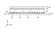
- FIG. 1 is a schematic sectional side view showing a configuration of a semiconductor device 100 according to an embodiment of the present invention.
- FIG. 2 is an enlarged view of a main part (first semiconductor package P1) in FIG.
- an X axis, a Y axis, and a Z axis indicate triaxial directions orthogonal to each other, and the Z axis direction corresponds to the height direction (thickness direction) of the semiconductor device 100.
- the semiconductor device 100 of this embodiment has a stacked structure (PoP: Package on Package) of a first semiconductor package P1 and a second semiconductor package P2.
- PoP Package on Package
- the first semiconductor package P1 includes a first wiring board 21 and a first semiconductor chip C1 that is flip-chip mounted (flip-chip connected) on the first wiring board 21.
- the second semiconductor package P2 is mounted on the first semiconductor package P1.
- the second semiconductor package P ⁇ b> 2 includes a second wiring substrate 22 and a second semiconductor chip C ⁇ b> 2 that is wire bonded to the second wiring substrate 22.
- the second semiconductor chip C2 has a stacked structure of two semiconductor chips C21 and C22 having different sizes.
- the first semiconductor chip C1 and the second semiconductor chip C2 are typically composed of a single crystal silicon (Si) substrate, and a plurality of circuit elements such as transistors and memories are integrated on the surface thereof. A circuitized circuit surface is formed.
- the first semiconductor chip C1 is mounted on the upper surface of the first wiring board 21 by a face-down method with its circuit surface facing the first wiring board 21.
- the first semiconductor chip C1 is electrically and mechanically connected to the first wiring substrate 21 via a plurality of bumps (projection electrodes) 41 formed on the circuit surface (lower surface in the drawing).
- a reflow soldering method using a reflow furnace is employed for joining the first semiconductor chip C1 to the first wiring board 21.
- An underfill resin layer 51 is typically provided between the first semiconductor chip C1 and the first wiring substrate 21.
- the underfill resin layer 51 seals the circuit surface of the first semiconductor chip C ⁇ b> 1 and the bumps 41 to shield them from the outside air, and further, the bonding strength between the first semiconductor chip C ⁇ b> 1 and the first wiring substrate 21. Is provided for the purpose of ensuring the connection reliability of the bumps 41 by increasing the resistance.
- a protective film for semiconductor (hereinafter referred to as a protective film) 10 for protecting the semiconductor chip C1 is provided on the back surface (the surface opposite to the circuit surface and the top surface in the figure) of the first semiconductor chip C1. It is stuck. As will be described later, the protective film 10 has a function of suppressing warping of the first semiconductor chip C1 and the first semiconductor package P1.
- the second semiconductor chip C2 (C21, C22) is mounted on the upper surface of the second wiring substrate 22 by a face-up method in which the back surface opposite to each circuit surface is directed to the second wiring substrate 22. Is done.
- the second semiconductor chip C2 (C21, C22) has a plurality of electrode pads (not shown) arranged around the circuit surface (upper surface in the drawing), and a plurality of electrode pads connected to each electrode pad. It is electrically connected to the second wiring board 22 via the bonding wire 42.
- the second wiring board 22 and the semiconductor chip C21, and the two semiconductor chips C21 and C22 are joined to each other by a non-conductive adhesive or the like.
- the sealing layer 52 for sealing the second semiconductor chip C2 (C21, C22) and the bonding wire 42 is provided on the upper surface of the second wiring board 22. Similarly to the underfill resin layer 51, the sealing layer 52 blocks the circuit surface of the second semiconductor chip C2 (C21, C22) from the outside air, and the second semiconductor chip C2 (C21, C22) and the second semiconductor chip C2 (C21, C22). It is provided for the purpose of improving the connection reliability with the wiring board 22.
- the first wiring board 21 and the second wiring board 22 may be made of the same material or different materials.
- the first wiring board 21 and the second wiring board 22 are typically configured by organic wiring boards such as a glass epoxy board and a polyimide board, but are not limited thereto, and a ceramic board or a metal board is used. May be.
- the type of wiring board is not particularly limited, and various boards such as a single-sided board, a double-sided board, a multilayer board, and an element-embedded board can be applied.
- the first and second wiring boards 21 and 22 are constituted by glass epoxy multilayer wiring boards having vias V1 and V2, respectively.
- a plurality of external connection terminals 31 connected to a control board 110 called a mother board or the like are provided on the back surface (lower surface in the drawing) of the first wiring board 21. That is, the first wiring substrate 21 is configured as an interposer substrate (daughter substrate) interposed between the first semiconductor chip C1 and the control substrate 110, and bumps on the circuit surface of the first semiconductor chip C1. It also has a function as a rewiring layer that converts the arrangement interval of 51 into the land pitch of the control board 110.
- a plurality of bumps 32 connected to the front surface of the first wiring substrate 21 are provided on the back surface (lower surface in the drawing) of the second wiring substrate 22. That is, the second wiring substrate 22 is configured as an interposer substrate that connects the second semiconductor chip C2 (C21, C22) to the first wiring substrate, and the first wiring substrate 21 and the external connection terminal 31 are interposed therebetween. , And electrically connected to the control board 110.
- the external connection terminal 31 and the bumps 41 and 32 are typically configured by solder bumps (ball bumps), but are not limited thereto, and may be configured by other protruding electrodes such as plating bumps and stud bumps. .
- a reflow soldering method is employed for the connection of the second wiring substrate 22 to the first wiring substrate 21 and the connection of the semiconductor device 100 to the control substrate 110.
- warp deformation of a semiconductor chip or a semiconductor device during reflow mounting is one of the important issues because it causes failure of electronic devices, mounting defects, and reduced reliability.
- a semiconductor device 100 having a PoP structure as shown in FIG. 1 since the first and second semiconductor packages P1 and P2 have a single-side sealing structure, warping is likely to occur.
- the first semiconductor package P1 located on the lower side is thinner than the second semiconductor package P2 located on the upper side, and the sealing region is partial.
- warpage is likely to occur in the first semiconductor package P1. If the first semiconductor package P1 is greatly warped during solder reflow, the bumps 32 of the second semiconductor package P2 may be separated from the first wiring board 21 and a connection failure may occur.
- the semiconductor device 100 of this embodiment has a function of suppressing the warp of the first semiconductor package P1 on the protective film 10 attached to the back surface of the first semiconductor chip C1. ing.
- the details of the protective film 10 will be described.
- FIG. 3 is a schematic sectional side view showing the protective film 10 according to one embodiment of the present invention.
- the protective film 10 is provided on the back surface of the first semiconductor chip C1.
- the protective film 10 is provided on the back surface of the first semiconductor chip C1, so that the rigidity of the first semiconductor chip C1 is improved, the back surface of the first semiconductor chip C1 is protected, and the type of the first semiconductor chip C1 is changed. It is configured to perform various functions such as display and warpage suppression of the first semiconductor package P1.
- the protective film 10 is typically attached to the back surface of the semiconductor wafer after the back grinding (back surface grinding) step and before dicing.
- the protective film 10 of this embodiment has a laminated structure of a protective layer 11 and an adhesive layer 12. As shown in FIG. 2, the protective film 10 is attached to the back surface of the first semiconductor chip C ⁇ b> 1 via the adhesive layer 12. The protective film 10 is formed by cutting out a wafer-sized protective film 10F (see FIG. 6A) attached to the back surface of a semiconductor wafer used for manufacturing the first semiconductor chip C1 at the chip level.
- the protective film according to the present invention can be used as a protective film for a semiconductor chip other than the semiconductor device shown in FIG.
- the protective layer 11 is configured as a base material for the protective film 10.
- the protective layer 11 is made of a nonconductive inorganic material.
- the non-conductive inorganic material is not particularly limited as long as it is suitable for workpiece processing, for example, dicing of a semiconductor wafer, and typically includes a vitreous material, a ceramic material, or a mixture thereof.
- the glassy material includes plate glass, glass fiber, and the like.
- the structure of the glass used for the plate glass or glass fiber may be amorphous or crystalline.
- the kind of glass is not particularly limited, and typical examples include soda lime glass, lead glass, borosilicate glass, and quartz glass.
- the plate glass for example, a thin plate glass for display, particularly an ultra-thin plate glass having flexibility that can be wound into a roll shape is preferable.
- the glass fiber for example, glass fiber configured as glass fiber paper (glass paper) or a battery material (separator) is applicable.
- the protective film 10 of the present embodiment increases the elastic modulus of the protective layer 11 as compared to the case where the protective layer 11 is made of a synthetic resin. Can do.
- the elastic modulus of the protective layer 11 is not particularly limited as long as it can typically suppress the warp of the first semiconductor package P1 during reflow mounting.
- the warpage of the first semiconductor package P1 is mainly caused by mismatching between the linear expansion coefficient of the first semiconductor chip C1 and the linear expansion coefficient of the first wiring substrate 21, and the difference between the two is larger. A large warp is induced.
- the direction of warpage varies depending on the type and characteristics of the material, but tends to be opposite to each other during heating and cooling.
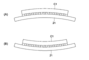
- FIGS. 4A and 4B are schematic views showing a slightly warped state of a semiconductor package not provided with a protective film.
- FIG. 4A shows a state at a normal temperature
- FIG. 4B shows a state at a high temperature. Therefore, it is preferable that the elastic modulus of the protective layer 11 can suppress warpage in both directions of the first semiconductor package P1.
- the first semiconductor chip C1 is made of a silicon substrate
- the first wiring board 21 is made of a glass epoxy organic material.
- the linear expansion coefficient ( ⁇ 10 ⁇ 6 / ° C.) of the first semiconductor chip C1 and the linear expansion coefficient ( ⁇ 10 ⁇ 5 / ° C.) of the first wiring board 21 are different by about one digit, and the first wiring board 21 However, the thermal expansion (thermal contraction) is larger than that of the first semiconductor chip C1.
- the linear expansion coefficient of the protective layer 11 may be set with reference to the linear expansion coefficient of the first wiring substrate 21 or may be set with reference to the linear expansion coefficient of the first semiconductor chip C1.
- the linear expansion coefficient of the protective layer 11 is matched with the linear expansion coefficient of the first wiring board 21 or is made smaller than the linear expansion coefficient of the first wiring board 21 to protect the first wiring board 21.
- the deformation of the first semiconductor chip C1 sandwiched between the film 10 can be suppressed.
- the rigidity of the first semiconductor chip C1 is adjusted by matching the linear expansion coefficient of the protective layer 11 with the linear expansion coefficient of the first semiconductor chip C1, or by making it smaller than the linear expansion coefficient of the first semiconductor chip C1.
- the linear expansion coefficient of the protective layer 11 may be set to an appropriate value between the linear expansion coefficient of the first wiring substrate 21 and the linear expansion coefficient of the first semiconductor chip C1.
- the warp of the first semiconductor package P1 can be effectively suppressed. What is necessary is just to select the nonelectroconductive inorganic material which comprises the protective layer 11 from the material from which the target linear expansion coefficient is obtained. Further, a plurality of types of non-conductive inorganic materials may be combined so as to obtain a target linear expansion coefficient.
- the protective layer 11 is made of a glassy material, and more specifically, is made of plate glass.
- the handleability of the protective film 10 is enhanced and the productivity is improved.
- a so-called tempered glass material may be used for the plate glass, or a normal glass material may be used.
- a rigid glass sheet may be used, or a flexible glass film may be used.
- a material having optical transparency is used for the plate glass, but a colored material may be used.
- the linear expansion coefficient of the protective layer 11 can be selected or adjusted according to the components of the plate glass constituting the protective layer 11, the processing method, and the like.
- the plate glass constituting the protective layer 11 can typically be selected from those having a linear expansion coefficient on the order of 10 ⁇ 5 to 10 ⁇ 7 / ° C.
- the softening point (Tg) of the vitreous material constituting the protective layer 11 is preferably higher than the reflow temperature (for example, 260 ° C. or higher). As a result, the softening and deformation of the protective layer 11 during reflow mounting can be suppressed, and the warpage suppressing effect of the semiconductor chip C1 can be maintained.
- the thickness of the protective layer 11 includes the size (thickness and size) of the first semiconductor chip C1, the size (thickness and size) of the first semiconductor package P1, the first semiconductor package P1 and the first semiconductor package C1. It is possible to set appropriately according to the gap between the two semiconductor packages P2.
- a plate glass having a flexibility of 10 ⁇ m or more and 300 ⁇ m or less, preferably 50 ⁇ m or more and 200 ⁇ m or less is used as the protective layer 11. As a result, it is possible to effectively prevent the warp deformation of the first semiconductor package P1 while ensuring the thinning of the first semiconductor package P1.
- the protective layer 11 has flexibility, the protective film 10 can be wound in a roll shape, and handling property, storage property, transportability and the like are improved.
- a flexible glass film has an advantage of excellent handling properties because it has little deformation such as curling when unwound from a roll.
- plate glass For such plate glass, commercially available materials may be used, or materials optimized according to applications may be used.
- a commercially available material for example, non-alkali ultrathin glass “G-Leaf” (registered trademark) manufactured by Nippon Electric Glass Co., Ltd. can be used.
- the adhesive layer 12 is provided on one surface of the protective layer 11.
- the adhesive layer 12 typically includes at least one of a thermosetting component and an energy ray curable component and a binder polymer component.
- thermosetting component examples include epoxy resin, phenol resin, melamine resin, urea resin, polyester resin, urethane resin, acrylic resin, polyimide resin, benzoxazine resin, and mixtures thereof.
- an epoxy resin, a phenol resin, and a mixture thereof are preferably used.
- bisphenol glycidyl type epoxy resin, o-cresol novolak type epoxy resin and phenol novolak type epoxy resin are preferably used. These epoxy resins can be used alone or in combination of two or more.
- the energy ray-curable component is composed of a compound that is polymerized and cured when irradiated with energy rays such as ultraviolet rays and electron beams.
- This compound has at least one polymerizable double bond in the molecule, and usually has a molecular weight of about 100 to 30,000, preferably about 300 to 10,000.
- energy beam polymerization type compounds include trimethylolpropane triacrylate, tetramethylolmethane tetraacrylate, pentaerythritol triacrylate, dipentaerythritol monohydroxypentaacrylate, dipentaerythritol hexaacrylate, and 1,4-butylene glycol.
- Diacrylate, 1,6-hexanediol diacrylate, polyethylene glycol diacrylate, oligoester acrylate, polyester-type or polyether-type urethane acrylate oligomer, polyester acrylate, polyether acrylate, epoxy-modified acrylate, and the like can be used.
- an ultraviolet curable resin is preferably used, and specifically, an oligoester acrylate, a urethane acrylate oligomer, or the like is particularly preferably used.
- an oligoester acrylate, a urethane acrylate oligomer, or the like is particularly preferably used.
- the binder polymer component is used to give an appropriate tack to the protective layer 11 and improve the operability of the sheet.
- the weight average molecular weight of the binder polymer is usually in the range of 50,000 to 2,000,000, preferably 100,000 to 1,500,000, particularly preferably 200,000 to 1,000,000. If the molecular weight is too low, sheet formation will be insufficient, and if it is too high, compatibility with other components will deteriorate, and as a result, uniform sheet formation will be hindered.
- binder polymer for example, an acrylic polymer, a polyester resin, a urethane resin, a silicone resin, a rubber polymer, and the like are used, and an acrylic polymer is particularly preferably used.
- the acrylic polymer examples include (meth) acrylic acid ester copolymers composed of structural units derived from (meth) acrylic acid ester monomers and (meth) acrylic acid derivatives.
- the (meth) acrylic acid ester monomer is preferably a (meth) acrylic acid alkyl ester having an alkyl group having 1 to 18 carbon atoms, such as methyl (meth) acrylate, ethyl (meth) acrylate, (meth) ) Propyl acrylate, butyl (meth) acrylate, etc. are used.
- the (meth) acrylic acid derivative include (meth) acrylic acid, glycidyl (meth) acrylate, hydroxyethyl (meth) acrylate, and the like.
- the adhesive layer 12 may be colored.
- the adhesive layer 12 is colored by, for example, blending a pigment, a dye, or the like. When the adhesive layer 12 is colored, the appearance can be improved and the visibility and distinguishability can be enhanced when laser printing is performed.
- the color of the adhesive layer 12 is not particularly limited, and may be an achromatic color or a chromatic color. In the present embodiment, the adhesive layer 12 is colored black.
- a coupling agent may be added to the adhesive layer 12 for the purpose of improving the adhesion and adhesion between the protective film 10 and the chip back surface after curing.
- a coupling agent can improve adhesiveness and adhesiveness without impairing the heat resistance of the protective film 10, and further improves water resistance (moisture heat resistance).
- a commercially available material may be used, or a material optimized according to the application may be used.
- a commercially available material for example, a chip back surface protection tape “LC tape” series (for example, LC2841, LC2824H, LC2826H, LC2850) manufactured by Lintec Corporation is preferably used.
- the protective film 10 of this embodiment further includes a release sheet 13.
- the release sheet 13 is provided so as to cover the adhesive layer 12, and is peeled from the adhesive layer 12 when the protective film 10 is used.
- Examples of the release sheet 13 include polyethylene film, polypropylene film, polybutene film, polybutadiene film, polymethylpentene film, polyvinyl chloride film, vinyl chloride copolymer film, polyethylene terephthalate film, polyethylene naphthalate film, and polybutylene terephthalate film. , Polyurethane film, ethylene vinyl acetate film, ionomer resin film, ethylene / (meth) acrylic acid copolymer film, ethylene / (meth) acrylic acid ester copolymer film, polystyrene film, polycarbonate film, polyimide film, fluororesin film, etc. Is used. These crosslinked films are also used. Furthermore, these laminated films may be sufficient.
- the surface tension of the release sheet 1 is preferably 40 mN / m or less, more preferably 37 mN / m or less, and particularly preferably 35 mN / m or less.
- a release sheet 13 having a low surface tension can be obtained by appropriately selecting the material, and can be obtained by applying a silicone resin or the like to the surface of the release sheet 13 and performing a release treatment. You can also.
- the thickness of the release sheet 13 is usually about 5 to 300 ⁇ m, preferably about 10 to 200 ⁇ m, particularly preferably about 20 to 150 ⁇ m.
- a commercially available material may be used, or a material optimized according to the application may be used.
- a commercially available material for example, a release film “D-645H” manufactured by Lintec Corporation is preferably used.
- a printing layer may be provided on at least one surface of the protective layer 11.
- the print layer typically includes characters, symbols, graphics, and the like, and displays the type of the semiconductor element or semiconductor device in an identifiable manner.
- the printing layer is typically composed of at least a part of the protective layer 11 or the adhesive layer 12, and is formed, for example, on the surface of the adhesive layer that is bonded to the protective layer.
- the printing layer may be formed, for example, by scraping the surface of the protective layer 11 by a laser processing method or the like, or may be formed by modifying the surface of the adhesive layer 12 by laser light irradiation.
- the protective layer 11 is made of a light-transmitting material such as plate glass or transparent ceramic, the protective layer 11 is provided with light-transmitting properties.
- the printing layer on the surface can be easily formed.
- the protective film 10 may have a printing layer separately. In other words, the print layer may be composed of a layer different from the protective layer 11 and the adhesive layer 12.
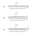
- FIGS. 5A to 5C are schematic cross-sectional side views illustrating a configuration example of a semiconductor device to which a protective film 10 having a printing layer is attached.
- FIG. 5A shows an example in which the printing layer 14 is provided on the lower surface (adhesive layer 12) of the protective layer 11.
- the printing layer 14 is composed of at least a part of the adhesive layer 12 and is formed by irradiating the adhesive layer 12 with an infrared laser (laser marking) from above the protective layer 11. Since the protective layer 11 is made of a glassy material having translucency, the infrared laser can easily reach the adhesive layer 12 via the protective layer 11.
- the print layer 14 is formed at the interface between the protective layer 11 and the adhesive layer 12 (surface on the adhesion side of the adhesive layer 12 to the protective layer 11), and can be recognized through the protective layer 11. Includes symbols or graphics.
- the print layer 14 typically displays the type of semiconductor chip or semiconductor device.
- FIG. 5B shows an example in which the printing layer 14 is provided on the upper surface of the protective layer 11.
- the printing layer 14 may be made of the same material as the adhesive layer 12 or may be made of a material different from the adhesive layer 12.
- the protective layer 11 may not transmit infrared rays.
- the laser marking on the print layer 14 may be performed before the adhesive layer 12 is cured, or may be performed after the adhesive layer 12 is cured.
- FIG. 5C shows an example in which the print layer 14 is provided on at least a part of the protective layer 11.
- the protective layer 11 is made of a light-transmitting non-conductive inorganic material such as a glassy material
- laser processing or surface processing using a micro cutter is possible.
- print information may be written on the surface of the protective layer 11 using a laser beam that can process the protective layer 11 (which can absorb a glassy material).
- the print layer 14 formed in this manner can make print information float on the surface of the protective layer 11 by viewing the protective layer 11 from the front or oblique direction.
- 6A to 6E are schematic process cross-sectional views illustrating a method for manufacturing the first semiconductor package P1.
- a protective film 10F is attached to the back surface (upper surface in the drawing) of the semiconductor wafer W thinned to a predetermined thickness (for example, 50 ⁇ m) by the back grinding process.
- the protective film 10 ⁇ / b> F is formed in, for example, a size and shape substantially the same as the semiconductor wafer W, and is attached to the back surface of the semiconductor wafer W via the adhesive layer 12.
- the release sheet 13 (see FIG. 3) of the protective film 10 is peeled from the adhesive layer 12 before being attached to the semiconductor wafer W. Thereafter, the adhesive layer 12 is cured by heat treatment or energy ray irradiation treatment.
- the protective film 10F By sticking the protective film 10F to the semiconductor wafer W, the apparent thickness of the semiconductor wafer W is increased. As a result, the rigidity of the semiconductor wafer W is increased and the handling property and dicing suitability are improved. As a result, the semiconductor wafer W is effectively protected from damage and cracks.
- a printing layer 14 (FIG. 5A) for displaying product information is formed on the protective film 10F.
- the print layer 14 is formed by irradiating the adhesive layer 12 with an infrared laser through the protective layer 11 (laser marking). By forming the printing layer 14 at the wafer level, predetermined product information can be efficiently printed on each chip area.
- the semiconductor wafer W to which the protective film 10F is bonded is mounted on the adhesive surface of the dicing tape T.
- the dicing tape T is disposed on a dicing table (not shown) provided on one surface of the dicing tape T with the adhesive layer facing upward, and is fixed by the ring frame F.
- the semiconductor wafer W is fixed on the dicing tape T via the protective film 10F with its circuit surface facing upward.
- the semiconductor wafer W is diced for each circuit (on a chip basis) by the dicer D.
- the blade of the dicer D cuts the semiconductor wafer W at a depth reaching the upper surface (adhesive surface) of the dicing tape T, whereby the protective film 10F is cut together with the semiconductor wafer W in units of chips.
- a protective film 10 corresponding to the chip C1 is formed.
- the semiconductor chip C ⁇ b> 1 is peeled from the adhesive layer of the dicing tape T together with the protective film 10 by the collet K. Thereafter, flux is attached to the circuit surface (bump) of the semiconductor chip C1, and as shown in FIG. 6E, the semiconductor chip (first semiconductor chip) C1 is connected to the wiring board (first semiconductor chip) using the mounter M. Flip chip mounting is performed on a wiring board 21.
- the protective film 10 is bonded to the back surface of the semiconductor chip C1, the apparent rigidity of the semiconductor chip C1 is increased, thereby improving the dicing suitability, the picking process from the dicing tape, Chip stress can be prevented from stress acting in the mounting process on the wiring board.
- the protective layer 11 is composed of a glassy material (non-conductive inorganic material), the dicing process is performed while improving the processing accuracy during dicing, as compared with the case where the protective layer 11 is composed of metal. Wear and deterioration of the saw (blade) can be suppressed. Further, even if the chips adhere to the circuit surface of the semiconductor chip C1, no short circuit failure occurs. As a result, productivity and reliability can be improved.
- the protective layer 11 is made of a vitreous material, warpage of the semiconductor chip C1 in the reflow mounting process of the semiconductor chip C1 on the wiring substrate 21 can be suppressed.
- FIGS. 7A and 7B show the evaluation results of the coplanarity of a semiconductor chip to which two protective films having different structures are attached.
- the silicon semiconductor chip used for the evaluation had a thickness of 50 ⁇ m and a size of 10 mm ⁇ 10 mm.
- the amount of warpage of the upper surface of the chip (the upper surface of the protective film) after reflow mounting on the glass epoxy wiring board was evaluated.
- IR reflow was performed three times with a preheating temperature of 130 ° C., a heating temperature (maximum temperature) of 260 ° C., and a heating time (holding time at the heating temperature) of 1 minute.
- a reflow furnace “WL-15-20DNX type” manufactured by Sagami Riko Co., Ltd. was used.
- “Thermoray PS200e” manufactured by Akrometrix was used as a coplanarity evaluation apparatus.
- a protective tape “LC2850” (hereinafter referred to as a protective tape) having a thickness of 25 ⁇ m is used as the protective film, and the sample shown in FIG. 7 (B) is used.
- a protective film a laminate (corresponding to the protective film 10 according to this embodiment) of the protective tape and a glass film having a thickness of 100 ⁇ m (Nippon Electric Glass Co., Ltd. ultra-thin glass “G-Leaf” (registered trademark)) ) was used.
- the warp of the chip was 214 ⁇ m, whereas in the sample shown in FIG. 7B, the warp of the chip was 56 ⁇ m.
- the amount of warpage of the chip when the thickness of the glass film was 50 ⁇ m was 111 ⁇ m.
- the warp amount of the chip when a 30 ⁇ m thick aluminum film was laminated was 106 ⁇ m
- the warp amount of the chip when an aluminum film of 40 ⁇ m thickness was laminated was 69 ⁇ m. It was.
- the first semiconductor package P1 with less warp can be manufactured stably. Therefore, even when the second semiconductor package P2 is mounted on the first semiconductor package P1 and the semiconductor device 100 is mounted on the control substrate 110, warping of the first semiconductor package P1 or the semiconductor device 100 is effectively suppressed. Therefore, it is possible to prevent the connection reliability of each terminal portion from being lowered due to warping deformation.
- FIG. 8 is a schematic sectional side view showing a configuration of a semiconductor device 200 according to another embodiment of the present invention.
- configurations different from those of the first embodiment will be mainly described, and configurations similar to those of the above-described embodiment will be denoted by the same reference numerals, and description thereof will be omitted or simplified.
- the semiconductor device 200 of this embodiment is common in that it has a PoP structure as in the first embodiment, but the base material 211 of the second wiring board 210 in the second semiconductor package P2 is made of a vitreous material. It differs from 1st Embodiment by the point comprised while being comprised as a protective layer of 1st semiconductor chip C1.
- the second wiring board 210 includes a base material 211, a wiring layer (via V2), and an adhesive layer 212.
- the substrate 211 is made of a vitreous material.
- the wiring layer includes a wiring pattern provided on the upper surface and the lower surface of the base material 211 and an interlayer connection portion (via V2) provided in the base material 211, and the first wiring substrate 21 and the second wiring layer 21 are provided.
- the semiconductor chip C2 (C21, C22) is electrically connected.
- the adhesive layer 212 is provided on the lower surface of the base material 211 and bonded to the back surface (upper surface in the drawing) of the first semiconductor chip C1.
- the thickness of the base material 211 is not particularly limited as long as a predetermined rigidity required for a wiring board can be ensured, and for example, a thickness of 50 ⁇ m or more and 300 ⁇ m or less is used.
- the form of the base material 211 is not particularly limited, and may be configured in a rigid sheet shape having high self-supporting property (self-supporting property) or may be configured in a film shape having flexibility.
- plate glass is used as the vitreous material constituting the substrate 211, but other than this, a laminated body of glass fibers, a sintered body of glass powder, or the like may be used.
- the base material 211 may be comprised with other nonelectroconductive inorganic materials other than a glassy material, for example, a ceramic board.
- the adhesive layer 212 is configured similarly to the first embodiment (adhesive layer 12).
- the adhesive layer 212 functions as a sealing layer that brings the base material 211 and the first semiconductor chip C1 into close contact with each other and blocks the back surface of the first semiconductor chip C1 from the outside air.
- the illustrated adhesive layer 212 is provided only in a region facing the back surface of the first semiconductor chip C1, but the present invention is not limited thereto, and the adhesive layer 212 may be provided over the entire lower surface of the base material 211. Good. In this case, an opening may be formed in the adhesive layer 212 at a position where the bump 32 is provided, or the adhesive layer 212 itself may be a conductive adhesive layer or an ACF (anisotropic conductive film) / ACP (anisotropic conductive film). It may be made of an anisotropic conductive material such as paste).
- the second wiring board 210 has the base material 211 made of a vitreous material, and the first semiconductor chip is interposed via the adhesive layer 212. Bonded to the back surface of C1.
- the warp of the first semiconductor chip C1 can be effectively suppressed, so that the warp deformation of the semiconductor device 200 can be prevented and the connection of each terminal portion can be prevented. Reliability can be increased.
- the adhesive layer 212 of the second wiring substrate 210 is bonded to the back surface of the first semiconductor chip C1, the first semiconductor package P1 and the second semiconductor package P2 As a result, the bonding reliability of the bumps 32 can be improved. Further, since the clearance between the second wiring substrate 210 and the first semiconductor chip C1 becomes zero, it is possible to contribute to the thinning of the semiconductor device 200.
- FIG. 9 is a schematic cross-sectional side view illustrating a configuration of a composite sheet 300 according to another embodiment of the present invention.
- configurations different from those of the first embodiment will be mainly described, and configurations similar to those of the above-described embodiment will be denoted by the same reference numerals, and description thereof will be omitted or simplified.
- the composite sheet 300 according to this embodiment is laminated on the pressure-sensitive adhesive sheet 70 in which the pressure-sensitive adhesive layer 72 is laminated on one surface of the base layer 71 and the pressure-sensitive adhesive sheet 70 on the pressure-sensitive adhesive layer 72 side.
- a protective film 10 is configured in the same manner as in the first embodiment, and is an adhesive provided on the surface of the protective layer 11 that is formed of a non-conductive inorganic material and on the surface opposite to the adhesive layer 74 side of the protective layer 11.
- the composite sheet 300 is used to form a protective film on the workpiece or a workpiece obtained by processing the workpiece while being attached to the workpiece and holding the workpiece when the workpiece is processed.
- This protective film is comprised from the protective film 10, Preferably, the protective film 10 which the adhesive bond layer 12 hardened
- the composite sheet 300 is used for holding a semiconductor wafer during dicing processing of a semiconductor wafer as a workpiece and forming a protective film on a semiconductor chip obtained by dicing, but is not limited thereto.
- the pressure-sensitive adhesive sheet 70 of the composite sheet 300 is generally referred to as a dicing sheet.
- the base layer 71 of the pressure-sensitive adhesive sheet 70 is not particularly limited as long as the base layer 71 is suitable for work processing, for example, dicing and expanding of a semiconductor wafer.
- a film mainly a resin-based material (Hereinafter referred to as “resin film”).
- resin films include polyethylene films such as low density polyethylene (LDPE) films, linear low density polyethylene (LLDPE) films, and high density polyethylene (HDPE) films, polypropylene films, polybutene films, polybutadiene films, and polymethylpentene films.
- LDPE low density polyethylene
- LLDPE linear low density polyethylene
- HDPE high density polyethylene
- Polyolefin films such as ethylene-norbornene copolymer film and norbornene resin film; ethylene-vinyl acetate copolymer film, ethylene- (meth) acrylic acid copolymer film, ethylene- (meth) acrylic acid ester copolymer
- Ethylene copolymer films such as films; Polyvinyl chloride films such as polyvinyl chloride films and vinyl chloride copolymer films; Polyethylene terephthalate films, Polybutylene films Polyester film such as terephthalate film; polyurethane film; polyimide film; polystyrene films; polycarbonate films; and fluorine resin film. Further, modified films such as these crosslinked films and ionomer films are also used.
- the base layer 71 may be a film made of one of these, or may be a laminated film in which two or more of these are combined.
- (meth) acrylic acid in the present specification means both acrylic acid and methacrylic acid. The same applies to other similar terms.
- polyolefin films are preferred from the viewpoints of environmental safety, cost, etc.
- polypropylene films having excellent heat resistance are preferred. If it is a polypropylene film, heat resistance can be imparted to the base layer 71 without impairing the expandability of the pressure-sensitive adhesive sheet 70 and the chip pickup property. Due to the heat resistance of the base layer 71, it is possible to suppress the occurrence of loosening of the pressure-sensitive adhesive sheet 70 even when the protective film 10 is heat-cured in a state where a workpiece is attached.
- the resin film may be subjected to a surface treatment such as an oxidation method or a concavo-convex method or a primer treatment on one or both sides as desired for the purpose of improving the adhesion with the pressure-sensitive adhesive layer 72 laminated on the surface.
- a surface treatment such as an oxidation method or a concavo-convex method or a primer treatment on one or both sides as desired for the purpose of improving the adhesion with the pressure-sensitive adhesive layer 72 laminated on the surface.
- a surface treatment such as an oxidation method or a concavo-convex method or a primer treatment on one or both sides as desired for the purpose of improving the adhesion with the pressure-sensitive adhesive layer 72 laminated on the surface.
- the oxidation method include corona discharge treatment, plasma discharge treatment, chromium oxidation treatment (wet), flame treatment, hot air treatment, ozone, ultraviolet irradiation treatment, and the like.
- a thermal spraying method include a thermal spraying method.
- the thickness of the base layer 71 is not particularly limited as long as it can function properly in each process in which the composite sheet 300 is used.
- the range is preferably 20 to 450 ⁇ m, more preferably 25 to 400 ⁇ m, and particularly preferably 50 to 350 ⁇ m.
- the pressure-sensitive adhesive layer 72 may be made of a non-energy ray curable pressure sensitive adhesive or may be made of an energy ray curable pressure sensitive adhesive.
- the non-energy ray curable pressure-sensitive adhesive those having desired adhesive strength and removability are preferable.
- Polyvinyl ether-based pressure-sensitive adhesives can be used.
- an acrylic pressure-sensitive adhesive that has high adhesion to the protective film 10 and that can effectively prevent the workpiece or workpiece from falling off in a dicing process or the like is preferable.
- the energy ray curable pressure-sensitive adhesive has an adhesive force that is reduced by energy beam irradiation. Therefore, when it is desired to separate the workpiece or workpiece and the pressure-sensitive adhesive sheet 70, it can be easily separated by irradiation with energy beam. it can.
- the thickness of the pressure-sensitive adhesive layer 72 is not particularly limited as long as it can function properly in each process in which the composite sheet 300 is used. Specifically, the thickness is preferably 1 to 50 ⁇ m, particularly preferably 2 to 30 ⁇ m, and further preferably 3 to 20 ⁇ m.
- a semiconductor (Si) chip has been described as an example of the semiconductor element.
- other semiconductor bare chip parts such as GaAs (gallium arsenide) may be used, or CSP (Chip Size).
- Package parts such as Package may be used.
- the adhesive bond layer 12 of the protective film 10 may also be comprised with the material containing nonelectroconductive inorganic materials, such as a vitreous material.
- the rigidity (elastic modulus) of the entire protective film 10 can be increased, warping of the first semiconductor chip C1 can be further suppressed.
Landscapes
- Dicing (AREA)
- Laminated Bodies (AREA)
- Adhesive Tapes (AREA)
- Adhesives Or Adhesive Processes (AREA)
- Wire Bonding (AREA)
- Structures Or Materials For Encapsulating Or Coating Semiconductor Devices Or Solid State Devices (AREA)
Abstract
Description
上記保護層は、非導電性無機材料で構成される。
上記接着剤層は、上記保護層の一方の面に設けられる。
また、保護層が非導電性無機材料で構成されているため、保護層が金属で構成される場合と比較して、ダイシング加工時における加工精度を向上させつつ、ダイシングソーの摩耗や劣化を抑制することができる。また、切り屑が半導体チップの回路面に付着したとしても短絡不良が生じることはない。これにより、生産性および信頼性の向上が図れることになる。
さらに、非導電性無機材料にガラス等の透光性を有する材料を用いることで、接着剤層表面にレーザー等で印字した場合にも、視認性を確保することが可能となる。
上記半導体素子は、上記配線基板にフリップチップ実装される。
上記保護フィルムは、非導電性無機材料で構成された保護層と、上記保護層の一方の面に設けられた接着剤層とを有し、上記接着剤層は上記半導体素子の裏面に接合される。
これにより、反りを抑制されたPoP構造等の半導体装置を得ることができる。
上記第1の半導体素子は、上記第1の配線基板にフリップチップ実装される。
上記第2の配線基板は、上記第1の半導体素子と上記第2の半導体素子との間に配置される。上記第2の配線基板は、保護層と、配線層と、接着剤層とを有する。上記保護層は、非導電性無機材料で構成される。上記配線層は、上記保護層に設けられ、上記第1の配線基板と上記第2の半導体素子との間を電気的に接続する。上記接着剤層は、上記保護層の一方の面に設けられ、上記第1の半導体素子の裏面に接合される。
上記保護フィルムは、非導電性無機材料で構成された保護層と、上記保護層の前記粘着層側とは反対側の面に設けられた接着剤層と、を有する。
図1は、本発明の一実施形態に係る半導体装置100の構成を示す概略側断面図、図2は、図1における要部(第1の半導体パッケージP1)の拡大図である。
各図において、X軸、Y軸及びZ軸は、相互に直交する3軸方向を示しており、Z軸方向は、半導体装置100の高さ方向(厚さ方向)に相当する。
図1に示すように、本実施形態の半導体装置100は、第1の半導体パッケージP1と第2の半導体パッケージP2との積層構造(PoP:Package on Package)を有する。
図3は、本発明の一実施形態に係る保護フィルム10を示す概略側断面図である。
なお、保護フィルム10は、第1の半導体チップC1の製造に用いられる半導体ウエハの裏面に貼着されたウエハサイズの保護フィルム10F(図6(A)参照)をチップレベルに切り出すことで形成される。なおまた、本発明に係る保護フィルムは、図1に示す半導体装置以外の半導体チップ用保護フィルムとして使用されることも、勿論可能である。
保護層11は、保護フィルム10の基材として構成される。保護層11は、非導電性無機材料で構成される。非導電性無機材料としては、ワークの加工、例えば半導体ウエハのダイシングに適するものであれば特に限定されず、典型的には、ガラス質材料、セラミック材料もしくはこれらの混合物などが挙げられる。
接着剤層12は、保護層11の一方の面に設けられる。接着剤層12は、典型的には、熱硬化性成分及びエネルギー線硬化性成分の少なくとも1種とバインダーポリマー成分とからなる。
図3に示すように、本実施形態の保護フィルム10は剥離シート13をさらに備える。剥離シート13は、接着剤層12を被覆するように設けられ、保護フィルム10の使用時には、接着剤層12から剥離される。
保護層11の少なくとも一方の面に印字層が設けられてもよい。印字層は、典型的には、文字、記号、図形等を含み、半導体素子あるいは半導体装置の種類等を識別可能に表示する。印字層は、典型的には、保護層11又は接着剤層12の少なくとも一部で構成され、例えば、接着剤層の保護層との接着側表面に形成される。印字層は、例えば、保護層11の表面をレーザー加工法等で削ることで形成されてもよいし、レーザー光の照射により接着剤層12表面を改質させることで形成されてもよい。特に、保護層11が板ガラス、透明セラミックス等、透光性を有する材料で構成される場合、保護層11に透光性が付与されるため、レーザー印字等により保護層の上から接着剤層12表面の印字層を容易に形成することができる。保護フィルム10は、印字層を別途有してもよい。すなわち、印字層は、保護層11及び接着剤層12とは異なる層で構成されてもよい。
続いて、保護フィルム10を備えた半導体装置、特に、第1の半導体パーケージP1の製造方法について説明する。
図8は、本発明の他の実施形態に係る半導体装置200の構成を示す概略側断面図である。以下、第1の実施形態と異なる構成について主に説明し、上述の実施形態と同様の構成については同様の符号を付しその説明を省略または簡略化する。
図9は、本発明の他の実施形態に係る複合シート300の構成を示す概略側断面図である。以下、第1の実施形態と異なる構成について主に説明し、上述の実施形態と同様の構成については同様の符号を付しその説明を省略または簡略化する。
保護フィルム10は、第1の実施形態と同様に構成され、非導電性無機材料で構成された保護層11と、保護層11の粘着層74側とは反対側の面に設けられた接着剤層12とを有する。
11…保護層
12,212…接着剤層
13…剥離シート
14…印字層
21…第1の配線基板
22,210…第2の配線基板
100,200…半導体装置
211…基材
300…複合シート
C1…第1の半導体チップ
C2…第2の半導体チップ
P1…第1の半導体パッケージ
P2…第2の半導体パッケージ
T…ダイシングテープ
W…半導体ウエハ
Claims (12)
- 非導電性無機材料で構成された保護層と、
前記保護層の一方の面に設けられた接着剤層と
を具備する半導体用保護フィルム。 - 請求項1に記載の半導体用保護フィルムであって、
前記非導電性無機材料は、少なくともガラス質材料を含む
半導体用保護フィルム。 - 請求項2に記載の半導体用保護フィルムであって、
前記保護層は、板ガラスで構成される
半導体用保護フィルム。 - 請求項1~3のいずれか1つに記載の半導体用保護フィルムであって、
前記保護層は、10μm以上300μm以下の厚さを有する
半導体用保護フィルム。 - 配線基板と、
前記配線基板にフリップチップ実装された半導体素子と、
非導電性無機材料で構成された保護層と、前記保護層の一方の面に設けられ前記半導体素子の裏面に接合された接着剤層とを有する保護フィルムと
を具備する半導体装置。 - 請求項5に記載の半導体装置であって、
前記保護層は、板ガラスで構成される
半導体装置。 - 請求項6に記載の半導体装置であって、
前記保護フィルムは、前記保護層の少なくとも一方の面に設けられた印字層を有する
半導体装置。 - 請求項7に記載の半導体装置であって、
前記印字層は、前記保護層又は前記接着剤層の少なくとも一部で構成される
半導体装置。 - 請求項5~8のいずれか1つに記載の半導体装置であって、
前記保護層は、10μm以上300μm以下の厚さを有する
半導体装置。 - 請求項5~9のいずれか1つに記載の半導体装置であって、
前記配線基板に電気的に接続される半導体パッケージ部品をさらに具備し、
前記半導体素子は、前記配線基板と前記半導体パッケージ部品との間に配置される
半導体装置。 - 第1の配線基板と、
前記第1の配線基板にフリップチップ実装された第1の半導体素子と、
第2の半導体素子と、
非導電性無機材料で構成された基材と、前記基材に設けられ前記第1の配線基板と前記第2の半導体素子との間を電気的に接続する配線層と、前記基材の一方の面に設けられ前記第1の半導体素子の裏面に接合された接着剤層とを有し、前記第1の半導体素子と前記第2の半導体素子との間に配置された第2の配線基板と
を具備する半導体装置。 - ベース層の一方の面側に粘着剤層が積層されてなる粘着シートと、
前記粘着シートの前記粘着層側に積層された保護フィルムと
を具備し、
前記保護フィルムは、
非導電性無機材料で構成された保護層と、
前記保護層の前記粘着層側とは反対側の面に設けられた接着剤層と、を有する
複合シート。
Priority Applications (3)
| Application Number | Priority Date | Filing Date | Title |
|---|---|---|---|
| CN201680031690.4A CN107636825B (zh) | 2015-06-04 | 2016-05-31 | 半导体用保护膜、半导体装置及复合片 |
| KR1020177036492A KR102201459B1 (ko) | 2015-06-04 | 2016-05-31 | 반도체용 보호 필름, 반도체 장치 및 복합 시트 |
| US15/578,156 US10825790B2 (en) | 2015-06-04 | 2016-05-31 | Protective film for semiconductors, semiconductor device, and composite sheet |
Applications Claiming Priority (2)
| Application Number | Priority Date | Filing Date | Title |
|---|---|---|---|
| JP2015-113907 | 2015-06-04 | ||
| JP2015113907A JP6571398B2 (ja) | 2015-06-04 | 2015-06-04 | 半導体用保護フィルム、半導体装置及び複合シート |
Publications (1)
| Publication Number | Publication Date |
|---|---|
| WO2016194893A1 true WO2016194893A1 (ja) | 2016-12-08 |
Family
ID=57441219
Family Applications (1)
| Application Number | Title | Priority Date | Filing Date |
|---|---|---|---|
| PCT/JP2016/065992 Ceased WO2016194893A1 (ja) | 2015-06-04 | 2016-05-31 | 半導体用保護フィルム、半導体装置及び複合シート |
Country Status (6)
| Country | Link |
|---|---|
| US (1) | US10825790B2 (ja) |
| JP (1) | JP6571398B2 (ja) |
| KR (1) | KR102201459B1 (ja) |
| CN (1) | CN107636825B (ja) |
| TW (1) | TWI646616B (ja) |
| WO (1) | WO2016194893A1 (ja) |
Families Citing this family (5)
| Publication number | Priority date | Publication date | Assignee | Title |
|---|---|---|---|---|
| CN113169127B (zh) * | 2019-05-15 | 2024-06-25 | 华为技术有限公司 | 一种芯片封装装置及其制备方法 |
| KR102757722B1 (ko) | 2020-05-22 | 2025-01-21 | 미쓰이 가가쿠 토세로 가부시키가이샤 | 점착성 적층 필름 및 전자 장치의 제조 방법 |
| CN118712146A (zh) * | 2021-04-22 | 2024-09-27 | 成都芯源系统有限公司 | 倒装芯片封装单元及相关封装方法 |
| CN115648532B (zh) * | 2022-10-31 | 2025-11-25 | 长电科技管理有限公司 | 半导体封装注塑模具、注塑装置及半导体封装注塑方法 |
| US20240379522A1 (en) * | 2023-05-09 | 2024-11-14 | Juniper Networks, Inc. | Semiconductor package with two substrates |
Citations (5)
| Publication number | Priority date | Publication date | Assignee | Title |
|---|---|---|---|---|
| JPH10294423A (ja) * | 1997-04-17 | 1998-11-04 | Nec Corp | 半導体装置 |
| JP2002208571A (ja) * | 2001-01-12 | 2002-07-26 | Matsushita Electric Ind Co Ltd | 半導体装置の製造方法および半導体装置 |
| JP2010199542A (ja) * | 2009-01-30 | 2010-09-09 | Nitto Denko Corp | ダイシングテープ一体型ウエハ裏面保護フィルム |
| US20110062599A1 (en) * | 2009-09-17 | 2011-03-17 | Joon Dong Kim | Integrated circuit packaging system with package stacking and method of manufacture thereof |
| JP2013041965A (ja) * | 2011-08-15 | 2013-02-28 | Fujikura Ltd | 半導体装置の製造方法 |
Family Cites Families (12)
| Publication number | Priority date | Publication date | Assignee | Title |
|---|---|---|---|---|
| JP2001135598A (ja) * | 1999-08-26 | 2001-05-18 | Seiko Epson Corp | ウエハのダイシング方法、半導体装置及びその製造方法、回路基板並びに電子機器 |
| JP2001326195A (ja) * | 2000-05-16 | 2001-11-22 | Hitachi Ltd | 半導体チップおよびその製造方法ならびに実装方法 |
| JP4432110B2 (ja) * | 2003-02-19 | 2010-03-17 | 日本電気硝子株式会社 | 半導体パッケージ用カバーガラス |
| JP2005298678A (ja) * | 2004-04-12 | 2005-10-27 | Fuji Photo Film Co Ltd | セリウム付活ホウ酸ルテチウム系輝尽性蛍光体、放射線像変換パネルおよび放射線画像記録再生方法 |
| JP4945902B2 (ja) * | 2005-01-24 | 2012-06-06 | 大日本印刷株式会社 | 化粧材 |
| CN101333070A (zh) * | 2007-06-28 | 2008-12-31 | 旭硝子株式会社 | 带电极的玻璃基板的制造方法 |
| US20090039532A1 (en) | 2007-08-08 | 2009-02-12 | Advanced Chip Engineering Technology Inc. | Semiconductor device package having a back side protective scheme |
| JP5733600B2 (ja) * | 2009-07-03 | 2015-06-10 | 日本電気硝子株式会社 | 素子封止体の製造方法、及び素子封止体 |
| JP5419226B2 (ja) | 2010-07-29 | 2014-02-19 | 日東電工株式会社 | フリップチップ型半導体裏面用フィルム及びその用途 |
| JP5820170B2 (ja) | 2011-07-13 | 2015-11-24 | 日東電工株式会社 | 半導体装置用の接着フィルム、フリップチップ型半導体裏面用フィルム、及び、ダイシングテープ一体型半導体裏面用フィルム |
| US9450203B2 (en) * | 2014-12-22 | 2016-09-20 | Apple Inc. | Organic light-emitting diode display with glass encapsulation and peripheral welded plastic seal |
| US20160201200A1 (en) * | 2015-01-14 | 2016-07-14 | Siemens Energy, Inc. | Adhesion of coatings using adhesive bonding compositions |
-
2015
- 2015-06-04 JP JP2015113907A patent/JP6571398B2/ja active Active
-
2016
- 2016-05-31 WO PCT/JP2016/065992 patent/WO2016194893A1/ja not_active Ceased
- 2016-05-31 KR KR1020177036492A patent/KR102201459B1/ko active Active
- 2016-05-31 CN CN201680031690.4A patent/CN107636825B/zh active Active
- 2016-05-31 US US15/578,156 patent/US10825790B2/en active Active
- 2016-06-03 TW TW105117571A patent/TWI646616B/zh active
Patent Citations (5)
| Publication number | Priority date | Publication date | Assignee | Title |
|---|---|---|---|---|
| JPH10294423A (ja) * | 1997-04-17 | 1998-11-04 | Nec Corp | 半導体装置 |
| JP2002208571A (ja) * | 2001-01-12 | 2002-07-26 | Matsushita Electric Ind Co Ltd | 半導体装置の製造方法および半導体装置 |
| JP2010199542A (ja) * | 2009-01-30 | 2010-09-09 | Nitto Denko Corp | ダイシングテープ一体型ウエハ裏面保護フィルム |
| US20110062599A1 (en) * | 2009-09-17 | 2011-03-17 | Joon Dong Kim | Integrated circuit packaging system with package stacking and method of manufacture thereof |
| JP2013041965A (ja) * | 2011-08-15 | 2013-02-28 | Fujikura Ltd | 半導体装置の製造方法 |
Also Published As
| Publication number | Publication date |
|---|---|
| KR20180002883A (ko) | 2018-01-08 |
| TWI646616B (zh) | 2019-01-01 |
| TW201707112A (zh) | 2017-02-16 |
| CN107636825B (zh) | 2020-11-24 |
| US20180138141A1 (en) | 2018-05-17 |
| CN107636825A (zh) | 2018-01-26 |
| JP2017001188A (ja) | 2017-01-05 |
| JP6571398B2 (ja) | 2019-09-04 |
| US10825790B2 (en) | 2020-11-03 |
| KR102201459B1 (ko) | 2021-01-11 |
Similar Documents
| Publication | Publication Date | Title |
|---|---|---|
| KR101933339B1 (ko) | 다이싱 테이프 일체형 반도체 이면용 필름 및 그의 제조 방법, 및 반도체 장치의 제조 방법 | |
| JP5487619B2 (ja) | 回路部材接続用接着剤及びこれを用いた半導体装置 | |
| TWI534236B (zh) | 用於半導體背面之切晶帶一體型薄膜 | |
| TWI527105B (zh) | 用於半導體背面之切晶帶一體型薄膜 | |
| JP5249290B2 (ja) | フリップチップ型半導体裏面用フィルム、ダイシングテープ一体型半導体裏面用フィルム、半導体装置の製造方法、及び、フリップチップ型半導体装置 | |
| JP6571398B2 (ja) | 半導体用保護フィルム、半導体装置及び複合シート | |
| JP6958791B2 (ja) | 半導体装置の製造方法 | |
| KR20150087222A (ko) | 반도체 칩의 제조방법 및 이것에 이용되는 박막 연삭용 표면 보호 테이프 | |
| CN102399505A (zh) | 切割/芯片接合薄膜 | |
| KR20120011319A (ko) | 반도체 장치 제조용 필름, 반도체 장치 제조용 필름의 제조 방법, 및 반도체 장치의 제조 방법 | |
| KR20120010124A (ko) | 플립칩형 반도체 이면용 필름 및 다이싱 테이프 일체형 반도체 이면용 필름 | |
| KR20140116204A (ko) | 플립 칩형 반도체 장치의 제조 방법 | |
| KR20120011780A (ko) | 다이싱 테이프 일체형 반도체 이면용 필름, 및 반도체 장치의 제조 방법 | |
| JP7319134B2 (ja) | 半導体素子の製造方法 | |
| CN104946146A (zh) | 芯片接合膜、带有切割片的芯片接合膜、半导体装置及半导体装置的制造方法 | |
| KR20120011822A (ko) | 플립 칩형 반도체 이면용 필름, 다이싱 테이프 일체형 반도체 이면용 필름, 반도체 장치의 제조 방법 및 플립 칩형 반도체 장치 | |
| JP2010245191A (ja) | フィルム状接着剤 | |
| JP5811514B2 (ja) | フィルム状接着剤 | |
| JP2010265416A (ja) | フィルム状接着剤 | |
| JP6440657B2 (ja) | 電子デバイス用テープ |
Legal Events
| Date | Code | Title | Description |
|---|---|---|---|
| 121 | Ep: the epo has been informed by wipo that ep was designated in this application |
Ref document number: 16803327 Country of ref document: EP Kind code of ref document: A1 |
|
| WWE | Wipo information: entry into national phase |
Ref document number: 15578156 Country of ref document: US |
|
| NENP | Non-entry into the national phase |
Ref country code: DE |
|
| ENP | Entry into the national phase |
Ref document number: 20177036492 Country of ref document: KR Kind code of ref document: A |
|
| 122 | Ep: pct application non-entry in european phase |
Ref document number: 16803327 Country of ref document: EP Kind code of ref document: A1 |