WO2016190007A1 - プラズマ原子層成長装置 - Google Patents
プラズマ原子層成長装置 Download PDFInfo
- Publication number
- WO2016190007A1 WO2016190007A1 PCT/JP2016/062402 JP2016062402W WO2016190007A1 WO 2016190007 A1 WO2016190007 A1 WO 2016190007A1 JP 2016062402 W JP2016062402 W JP 2016062402W WO 2016190007 A1 WO2016190007 A1 WO 2016190007A1
- Authority
- WO
- WIPO (PCT)
- Prior art keywords
- deposition
- exhaust
- injector
- atomic layer
- layer growth
- Prior art date
- Legal status (The legal status is an assumption and is not a legal conclusion. Google has not performed a legal analysis and makes no representation as to the accuracy of the status listed.)
- Ceased
Links
Images



Classifications
-
- C—CHEMISTRY; METALLURGY
- C23—COATING METALLIC MATERIAL; COATING MATERIAL WITH METALLIC MATERIAL; CHEMICAL SURFACE TREATMENT; DIFFUSION TREATMENT OF METALLIC MATERIAL; COATING BY VACUUM EVAPORATION, BY SPUTTERING, BY ION IMPLANTATION OR BY CHEMICAL VAPOUR DEPOSITION, IN GENERAL; INHIBITING CORROSION OF METALLIC MATERIAL OR INCRUSTATION IN GENERAL
- C23C—COATING METALLIC MATERIAL; COATING MATERIAL WITH METALLIC MATERIAL; SURFACE TREATMENT OF METALLIC MATERIAL BY DIFFUSION INTO THE SURFACE, BY CHEMICAL CONVERSION OR SUBSTITUTION; COATING BY VACUUM EVAPORATION, BY SPUTTERING, BY ION IMPLANTATION OR BY CHEMICAL VAPOUR DEPOSITION, IN GENERAL
- C23C16/00—Chemical coating by decomposition of gaseous compounds, without leaving reaction products of surface material in the coating, i.e. chemical vapour deposition [CVD] processes
- C23C16/44—Chemical coating by decomposition of gaseous compounds, without leaving reaction products of surface material in the coating, i.e. chemical vapour deposition [CVD] processes characterised by the method of coating
- C23C16/50—Chemical coating by decomposition of gaseous compounds, without leaving reaction products of surface material in the coating, i.e. chemical vapour deposition [CVD] processes characterised by the method of coating using electric discharges
-
- C—CHEMISTRY; METALLURGY
- C23—COATING METALLIC MATERIAL; COATING MATERIAL WITH METALLIC MATERIAL; CHEMICAL SURFACE TREATMENT; DIFFUSION TREATMENT OF METALLIC MATERIAL; COATING BY VACUUM EVAPORATION, BY SPUTTERING, BY ION IMPLANTATION OR BY CHEMICAL VAPOUR DEPOSITION, IN GENERAL; INHIBITING CORROSION OF METALLIC MATERIAL OR INCRUSTATION IN GENERAL
- C23C—COATING METALLIC MATERIAL; COATING MATERIAL WITH METALLIC MATERIAL; SURFACE TREATMENT OF METALLIC MATERIAL BY DIFFUSION INTO THE SURFACE, BY CHEMICAL CONVERSION OR SUBSTITUTION; COATING BY VACUUM EVAPORATION, BY SPUTTERING, BY ION IMPLANTATION OR BY CHEMICAL VAPOUR DEPOSITION, IN GENERAL
- C23C16/00—Chemical coating by decomposition of gaseous compounds, without leaving reaction products of surface material in the coating, i.e. chemical vapour deposition [CVD] processes
- C23C16/22—Chemical coating by decomposition of gaseous compounds, without leaving reaction products of surface material in the coating, i.e. chemical vapour deposition [CVD] processes characterised by the deposition of inorganic material, other than metallic material
- C23C16/30—Deposition of compounds, mixtures or solid solutions, e.g. borides, carbides, nitrides
- C23C16/308—Oxynitrides
-
- C—CHEMISTRY; METALLURGY
- C23—COATING METALLIC MATERIAL; COATING MATERIAL WITH METALLIC MATERIAL; CHEMICAL SURFACE TREATMENT; DIFFUSION TREATMENT OF METALLIC MATERIAL; COATING BY VACUUM EVAPORATION, BY SPUTTERING, BY ION IMPLANTATION OR BY CHEMICAL VAPOUR DEPOSITION, IN GENERAL; INHIBITING CORROSION OF METALLIC MATERIAL OR INCRUSTATION IN GENERAL
- C23C—COATING METALLIC MATERIAL; COATING MATERIAL WITH METALLIC MATERIAL; SURFACE TREATMENT OF METALLIC MATERIAL BY DIFFUSION INTO THE SURFACE, BY CHEMICAL CONVERSION OR SUBSTITUTION; COATING BY VACUUM EVAPORATION, BY SPUTTERING, BY ION IMPLANTATION OR BY CHEMICAL VAPOUR DEPOSITION, IN GENERAL
- C23C16/00—Chemical coating by decomposition of gaseous compounds, without leaving reaction products of surface material in the coating, i.e. chemical vapour deposition [CVD] processes
- C23C16/44—Chemical coating by decomposition of gaseous compounds, without leaving reaction products of surface material in the coating, i.e. chemical vapour deposition [CVD] processes characterised by the method of coating
- C23C16/4401—Means for minimising impurities, e.g. dust, moisture or residual gas, in the reaction chamber
-
- C—CHEMISTRY; METALLURGY
- C23—COATING METALLIC MATERIAL; COATING MATERIAL WITH METALLIC MATERIAL; CHEMICAL SURFACE TREATMENT; DIFFUSION TREATMENT OF METALLIC MATERIAL; COATING BY VACUUM EVAPORATION, BY SPUTTERING, BY ION IMPLANTATION OR BY CHEMICAL VAPOUR DEPOSITION, IN GENERAL; INHIBITING CORROSION OF METALLIC MATERIAL OR INCRUSTATION IN GENERAL
- C23C—COATING METALLIC MATERIAL; COATING MATERIAL WITH METALLIC MATERIAL; SURFACE TREATMENT OF METALLIC MATERIAL BY DIFFUSION INTO THE SURFACE, BY CHEMICAL CONVERSION OR SUBSTITUTION; COATING BY VACUUM EVAPORATION, BY SPUTTERING, BY ION IMPLANTATION OR BY CHEMICAL VAPOUR DEPOSITION, IN GENERAL
- C23C16/00—Chemical coating by decomposition of gaseous compounds, without leaving reaction products of surface material in the coating, i.e. chemical vapour deposition [CVD] processes
- C23C16/44—Chemical coating by decomposition of gaseous compounds, without leaving reaction products of surface material in the coating, i.e. chemical vapour deposition [CVD] processes characterised by the method of coating
- C23C16/4412—Details relating to the exhausts, e.g. pumps, filters, scrubbers, particle traps
-
- C—CHEMISTRY; METALLURGY
- C23—COATING METALLIC MATERIAL; COATING MATERIAL WITH METALLIC MATERIAL; CHEMICAL SURFACE TREATMENT; DIFFUSION TREATMENT OF METALLIC MATERIAL; COATING BY VACUUM EVAPORATION, BY SPUTTERING, BY ION IMPLANTATION OR BY CHEMICAL VAPOUR DEPOSITION, IN GENERAL; INHIBITING CORROSION OF METALLIC MATERIAL OR INCRUSTATION IN GENERAL
- C23C—COATING METALLIC MATERIAL; COATING MATERIAL WITH METALLIC MATERIAL; SURFACE TREATMENT OF METALLIC MATERIAL BY DIFFUSION INTO THE SURFACE, BY CHEMICAL CONVERSION OR SUBSTITUTION; COATING BY VACUUM EVAPORATION, BY SPUTTERING, BY ION IMPLANTATION OR BY CHEMICAL VAPOUR DEPOSITION, IN GENERAL
- C23C16/00—Chemical coating by decomposition of gaseous compounds, without leaving reaction products of surface material in the coating, i.e. chemical vapour deposition [CVD] processes
- C23C16/44—Chemical coating by decomposition of gaseous compounds, without leaving reaction products of surface material in the coating, i.e. chemical vapour deposition [CVD] processes characterised by the method of coating
- C23C16/455—Chemical coating by decomposition of gaseous compounds, without leaving reaction products of surface material in the coating, i.e. chemical vapour deposition [CVD] processes characterised by the method of coating characterised by the method used for introducing gases into reaction chamber or for modifying gas flows in reaction chamber
- C23C16/45523—Pulsed gas flow or change of composition over time
- C23C16/45525—Atomic layer deposition [ALD]
- C23C16/45527—Atomic layer deposition [ALD] characterized by the ALD cycle, e.g. different flows or temperatures during half-reactions, unusual pulsing sequence, use of precursor mixtures or auxiliary reactants or activations
- C23C16/45536—Use of plasma, radiation or electromagnetic fields
-
- C—CHEMISTRY; METALLURGY
- C23—COATING METALLIC MATERIAL; COATING MATERIAL WITH METALLIC MATERIAL; CHEMICAL SURFACE TREATMENT; DIFFUSION TREATMENT OF METALLIC MATERIAL; COATING BY VACUUM EVAPORATION, BY SPUTTERING, BY ION IMPLANTATION OR BY CHEMICAL VAPOUR DEPOSITION, IN GENERAL; INHIBITING CORROSION OF METALLIC MATERIAL OR INCRUSTATION IN GENERAL
- C23C—COATING METALLIC MATERIAL; COATING MATERIAL WITH METALLIC MATERIAL; SURFACE TREATMENT OF METALLIC MATERIAL BY DIFFUSION INTO THE SURFACE, BY CHEMICAL CONVERSION OR SUBSTITUTION; COATING BY VACUUM EVAPORATION, BY SPUTTERING, BY ION IMPLANTATION OR BY CHEMICAL VAPOUR DEPOSITION, IN GENERAL
- C23C16/00—Chemical coating by decomposition of gaseous compounds, without leaving reaction products of surface material in the coating, i.e. chemical vapour deposition [CVD] processes
- C23C16/44—Chemical coating by decomposition of gaseous compounds, without leaving reaction products of surface material in the coating, i.e. chemical vapour deposition [CVD] processes characterised by the method of coating
- C23C16/455—Chemical coating by decomposition of gaseous compounds, without leaving reaction products of surface material in the coating, i.e. chemical vapour deposition [CVD] processes characterised by the method of coating characterised by the method used for introducing gases into reaction chamber or for modifying gas flows in reaction chamber
- C23C16/45523—Pulsed gas flow or change of composition over time
- C23C16/45525—Atomic layer deposition [ALD]
- C23C16/45544—Atomic layer deposition [ALD] characterized by the apparatus
-
- C—CHEMISTRY; METALLURGY
- C23—COATING METALLIC MATERIAL; COATING MATERIAL WITH METALLIC MATERIAL; CHEMICAL SURFACE TREATMENT; DIFFUSION TREATMENT OF METALLIC MATERIAL; COATING BY VACUUM EVAPORATION, BY SPUTTERING, BY ION IMPLANTATION OR BY CHEMICAL VAPOUR DEPOSITION, IN GENERAL; INHIBITING CORROSION OF METALLIC MATERIAL OR INCRUSTATION IN GENERAL
- C23C—COATING METALLIC MATERIAL; COATING MATERIAL WITH METALLIC MATERIAL; SURFACE TREATMENT OF METALLIC MATERIAL BY DIFFUSION INTO THE SURFACE, BY CHEMICAL CONVERSION OR SUBSTITUTION; COATING BY VACUUM EVAPORATION, BY SPUTTERING, BY ION IMPLANTATION OR BY CHEMICAL VAPOUR DEPOSITION, IN GENERAL
- C23C16/00—Chemical coating by decomposition of gaseous compounds, without leaving reaction products of surface material in the coating, i.e. chemical vapour deposition [CVD] processes
- C23C16/44—Chemical coating by decomposition of gaseous compounds, without leaving reaction products of surface material in the coating, i.e. chemical vapour deposition [CVD] processes characterised by the method of coating
- C23C16/455—Chemical coating by decomposition of gaseous compounds, without leaving reaction products of surface material in the coating, i.e. chemical vapour deposition [CVD] processes characterised by the method of coating characterised by the method used for introducing gases into reaction chamber or for modifying gas flows in reaction chamber
- C23C16/45563—Gas nozzles
-
- C—CHEMISTRY; METALLURGY
- C23—COATING METALLIC MATERIAL; COATING MATERIAL WITH METALLIC MATERIAL; CHEMICAL SURFACE TREATMENT; DIFFUSION TREATMENT OF METALLIC MATERIAL; COATING BY VACUUM EVAPORATION, BY SPUTTERING, BY ION IMPLANTATION OR BY CHEMICAL VAPOUR DEPOSITION, IN GENERAL; INHIBITING CORROSION OF METALLIC MATERIAL OR INCRUSTATION IN GENERAL
- C23C—COATING METALLIC MATERIAL; COATING MATERIAL WITH METALLIC MATERIAL; SURFACE TREATMENT OF METALLIC MATERIAL BY DIFFUSION INTO THE SURFACE, BY CHEMICAL CONVERSION OR SUBSTITUTION; COATING BY VACUUM EVAPORATION, BY SPUTTERING, BY ION IMPLANTATION OR BY CHEMICAL VAPOUR DEPOSITION, IN GENERAL
- C23C16/00—Chemical coating by decomposition of gaseous compounds, without leaving reaction products of surface material in the coating, i.e. chemical vapour deposition [CVD] processes
- C23C16/44—Chemical coating by decomposition of gaseous compounds, without leaving reaction products of surface material in the coating, i.e. chemical vapour deposition [CVD] processes characterised by the method of coating
- C23C16/455—Chemical coating by decomposition of gaseous compounds, without leaving reaction products of surface material in the coating, i.e. chemical vapour deposition [CVD] processes characterised by the method of coating characterised by the method used for introducing gases into reaction chamber or for modifying gas flows in reaction chamber
- C23C16/45563—Gas nozzles
- C23C16/45565—Shower nozzles
-
- H—ELECTRICITY
- H01—ELECTRIC ELEMENTS
- H01J—ELECTRIC DISCHARGE TUBES OR DISCHARGE LAMPS
- H01J37/00—Discharge tubes with provision for introducing objects or material to be exposed to the discharge, e.g. for the purpose of examination or processing thereof
- H01J37/32—Gas-filled discharge tubes
- H01J37/32431—Constructional details of the reactor
- H01J37/3244—Gas supply means
-
- H—ELECTRICITY
- H01—ELECTRIC ELEMENTS
- H01J—ELECTRIC DISCHARGE TUBES OR DISCHARGE LAMPS
- H01J37/00—Discharge tubes with provision for introducing objects or material to be exposed to the discharge, e.g. for the purpose of examination or processing thereof
- H01J37/32—Gas-filled discharge tubes
- H01J37/32431—Constructional details of the reactor
- H01J37/32458—Vessel
- H01J37/32477—Vessel characterised by the means for protecting vessels or internal parts, e.g. coatings
-
- H—ELECTRICITY
- H01—ELECTRIC ELEMENTS
- H01J—ELECTRIC DISCHARGE TUBES OR DISCHARGE LAMPS
- H01J37/00—Discharge tubes with provision for introducing objects or material to be exposed to the discharge, e.g. for the purpose of examination or processing thereof
- H01J37/32—Gas-filled discharge tubes
- H01J37/32431—Constructional details of the reactor
- H01J37/32458—Vessel
- H01J37/32477—Vessel characterised by the means for protecting vessels or internal parts, e.g. coatings
- H01J37/32486—Means for reducing recombination coefficient
-
- H—ELECTRICITY
- H01—ELECTRIC ELEMENTS
- H01J—ELECTRIC DISCHARGE TUBES OR DISCHARGE LAMPS
- H01J37/00—Discharge tubes with provision for introducing objects or material to be exposed to the discharge, e.g. for the purpose of examination or processing thereof
- H01J37/32—Gas-filled discharge tubes
- H01J37/32431—Constructional details of the reactor
- H01J37/32798—Further details of plasma apparatus not provided for in groups H01J37/3244 - H01J37/32788; special provisions for cleaning or maintenance of the apparatus
- H01J37/32816—Pressure
- H01J37/32834—Exhausting
-
- H—ELECTRICITY
- H01—ELECTRIC ELEMENTS
- H01J—ELECTRIC DISCHARGE TUBES OR DISCHARGE LAMPS
- H01J37/00—Discharge tubes with provision for introducing objects or material to be exposed to the discharge, e.g. for the purpose of examination or processing thereof
- H01J37/32—Gas-filled discharge tubes
- H01J37/32431—Constructional details of the reactor
- H01J37/32798—Further details of plasma apparatus not provided for in groups H01J37/3244 - H01J37/32788; special provisions for cleaning or maintenance of the apparatus
- H01J37/3288—Maintenance
Definitions
- the present invention relates to a plasma atomic layer growth apparatus for forming a thin film on a substrate.
- Atomic layer growth is known as a technique for uniformly forming a thin film by alternately supplying the gas of the elements that make up the thin film to be formed onto the substrate and forming the thin film in atomic layers on the substrate. ing.
- the atomic layer growth method is superior in step coverage and film thickness controllability as compared with a general CVD (Chemical Vapor Deposition) method.
- CVD Chemical Vapor Deposition
- the thin film also adheres to the inner surface of the film formation container.
- the thickness of the thin film adhering to the inner surface of the film formation container is increased, the deposited thin film is peeled off, and a part thereof becomes particles, which causes the quality of the thin film formed on the substrate to deteriorate. Therefore, it is preferable to periodically remove the thin film adhering to the inner surface of the film formation container.
- a vapor deposition apparatus such as a CVD film formation or a sputter film formation uses a deposition plate and further includes a processing method and apparatus for covering deposits deposited on the inner wall of a chamber with an amorphous film. Proposed.
- the conventional vapor phase growth apparatus it is possible to reduce the frequency of cleaning by such means, but the deposit deposited on the inner wall of the chamber and the thickness of the amorphous film covering the deposit are more than a predetermined thickness. In this case, it is necessary to perform cleaning using a wet etching method.
- the wet etching method since the film formation container is opened, as the film formation container becomes larger, the work of opening work becomes larger.
- the gas etching method should be used. Is preferred. In order to perform etching by the gas etching method, it is necessary to heat the thin film adhering portion on the inner wall surface of the film formation container to a predetermined temperature or more, but in a portion away from the heater, the required heating temperature is not reached, It becomes difficult to perform gas etching. For this reason, when a certain amount of thin film adheres to a place where gas etching is difficult to perform, it is necessary to open the film formation container and perform wet etching.
- the deposition preventing plate is divided and installed in the film forming container. Dividing the protective plate makes it easy to handle, and in the case of a device that heats to a high temperature, the thermal expansion of the protective plate can be absorbed by providing a space in the gap between the divided protective plates. Is possible.
- the source gas and the reaction gas finely enter the gap easily to form a film. The gas that has entered such fine gaps becomes a film and powder, which causes particles. Therefore, in the atomic layer growth apparatus, it is preferable to suppress the division of the deposition preventing plate as much as possible.
- Patent Document 3 In order to suppress film formation when it is necessary to divide the deposition preventive plate, for example, as shown in Patent Document 3, a method of supplying an inert gas can be used. In addition, in atomic layer growth film formation without using plasma, it is possible to protect the upper portion of the substrate by using the deposition preventing plate shown in Patent Document 4.
- an insulator is used to support the electrode to which a high frequency is applied.
- a resin such as Teflon (registered trademark) or ceramics is mainly used.
- the insulating support that fixes the upper electrode can be regenerated by wet etching, but by disassembling the support and reconstructing the flat plate electrode, the mounting position of the flat plate electrode changes from the previous mounting position, and the plasma The state may change from before maintenance. Therefore, maintenance of the insulating support is not preferable, and it is preferable that it is maintenance-free. Therefore, it is conceivable to use an insulating deposition preventing plate for the insulating support. In that case, the insulating deposition preventing plate is fixed by a fixing means such as a screw. However, in atomic layer growth, a film is easily formed in, for example, a screw hole, so that the screw is firmly fixed by the force of the film.
- the present invention provides a plasma atomic layer growth apparatus capable of reducing the frequency of cleaning of a deposition container and a deposition material inside the deposition container, reducing the number of maintenance parts, and improving maintenance workability. Objective.
- the first form is A deposition container; A plate electrode provided to face the substrate held in the film formation container; A counter electrode for holding a substrate inside the film formation container; A gas introduction opening provided in one side wall of the film formation container, and an exhaust opening provided in the other side wall of the film formation container facing the one side wall, A plasma atomic layer growth apparatus for forming a thin film on the substrate, An insulating injector deposition material that can be attached to the gas introduction opening from the inside of the film formation container and is disposed in a cylindrical shape so as to surround the opening of the gas introduction opening, Insulating exhaust deposition preventive material that can be attached to the exhaust opening from the inside of the film formation container and is arranged in a cylindrical shape so as to surround the opening of the exhaust opening, An insulating film-forming chamber deposition material that can be attached to the inner wall side of the film-forming container; The injector adhesion preventing material is There is a gap between the plate electrode and the counter electrode side, and the tip is
- An inert gas supply port A lower inert gas that purges an inert gas from the gap between the counter electrode, the injector adhesion material, the exhaust adhesion material, and the film formation chamber adhesion material toward the inside of the film formation container.
- the invention of the plasma atomic layer growth apparatus of another form is the present invention of the above form,
- the injector adhesion preventing material is Based on the plate electrode end on the gas introduction opening side, the tip position extends from the plate electrode end to the center of the plate electrode in a range of 0.1 mm or more and 200 mm or less,
- the exhaust gas-proofing material is The tip end position extends from the plate electrode end toward the center of the plate electrode in a range of 0.1 mm or more and 200 mm or less from the plate electrode end on the exhaust opening side.
- the invention of the plasma atomic layer growth apparatus of another form is the present invention of the above form,
- the side end portion of the cylindrical opening by the injector adhesion preventing material has a distance of 0.1 mm or more and 200 mm or less outward from the side end portion of the substrate held by the counter electrode,
- a side end portion of the cylindrical opening portion formed by the exhaust deposition preventing material has a distance of 0.1 mm or more and 200 mm or less outward from a side end portion of the substrate held by the counter electrode. .
- the invention of the plasma atomic layer growth apparatus of another form is the present invention of the above form,
- the film formation chamber deposition material has a size that covers a vertical width of a side portion of the injector deposition protection material and a side portion of the exhaust deposition protection material, and an inner side surface of the deposition chamber deposition material.
- the outer surface of the injector adhesion preventing material has a gap of a horizontal distance of 0.1 mm or more and 20 mm or less, and the inner surface of the deposition chamber adhesion preventing material and the outer surface of the exhaust adhesion preventing material are 0.1 mm or more.
- the invention of the plasma atomic layer growth apparatus of another form is the present invention of the above form,
- the film formation chamber deposition material and the injector deposition material have an overlap of 0.1 mm or more and 200 mm or less in the gas flow direction between the gas introduction opening and the exhaust opening,
- the deposition chamber deposition material and the exhaust deposition material have an overlap of 0.1 mm or more and 200 mm or less in the gas flow direction between the gas introduction opening and the exhaust opening.
- the invention of the plasma atomic layer growth apparatus of another form is the present invention of the above form,
- the injector adhesion preventing material has a lateral outer surface located on the inner side at a distance of 0.1 mm or more and 200 mm or less with respect to a side edge of the flat plate electrode.
- the exhaust deposition preventive material is characterized in that a lateral outer surface is located on the inner side at a distance of 0.1 mm or more and 200 mm or less with respect to a side end of the plate electrode end.
- the invention of the plasma atomic layer growth apparatus of another form is the present invention of the above form,
- the film formation chamber deposition material, the injector deposition material, and the exhaust deposition protection material are disposed in the film deposition container so as to have a fixed end portion with respect to the film deposition container at a distance of 50 mm or more from the adjacent plate electrode end. It is attached and fixed.
- the deposition chamber deposition material has a length that spans the injector deposition material and the exhaust deposition material.
- the invention of the plasma atomic layer growth apparatus of another form is the present invention of the above form,
- the upper inert gas supply unit and the lower inert gas supply unit are respectively connected to the upper inert gas supply port and the lower inert gas supply port by a shower head structure.
- the invention of the plasma atomic layer growth apparatus of another form is the present invention of the above form,
- the upper surface of the injector anti-adhesive material and the upper surface of the exhaust anti-adhesive material and the lower surface on the flat plate electrode side have a vertical distance of 0.1 mm or more and 20 mm or less.
- the invention of the plasma atomic layer growth apparatus of another form is the present invention of the above form,
- the injector anti-adhesive material and the exhaust anti-adhesion material are zero in horizontal distance from the adjacent end of the substrate held by the counter electrode in the gas flow direction between the gas introduction part and the exhaust part. It has a gap of 1 mm or more and 200 mm or less.
- the invention of the plasma atomic layer growth apparatus of another form is the present invention of the above form,
- the lower surface of the injector anti-adhesive material and the lower surface of the exhaust anti-adhesive material and the upper surface on the counter electrode side have a vertical distance of 0.1 mm or more and 20 mm or less.
- the invention of the plasma atomic layer growth apparatus of another form is the present invention of the above form,
- the counter electrode has a counter electrode holding portion having a holding surface for holding the substrate, and a counter electrode peripheral portion around the counter electrode holding portion and having a height lower than the counter electrode holding surface. It is characterized by.
- the present invention it is possible to reduce the deposition area inside the deposition container, and it is possible to suppress the generation of particles and reduce the frequency of cleaning the deposition container and the deposition material.
- FIG. 1 is a schematic configuration diagram showing an example of a plasma atomic layer growth apparatus of the present embodiment.
- the plasma atomic layer growth apparatus 10 of this embodiment supplies a source gas and a reactive gas alternately, and forms a thin film on the substrate 100 in units of atomic layers. At that time, the substrate 100 can be heated to increase the reaction activity.
- TMA Tri-Methyl-Aluminum
- parallel plate electrodes are used for plasma generation.
- the film forming container 11 includes an injector 21, an exhaust flange 31, a flat plate electrode 12, a counter electrode 14, and a high frequency power source 16.
- the counter electrode 14 includes a stage heater 14 ⁇ / b> A and can adjust the temperature of the substrate 100. For example, in the case of a plasma atomic layer growth apparatus, the substrate 100 is heated to 50 to 200.degree.
- the film formation container 11 is maintained in a vacuum during processing.
- the plate electrode 12 is provided above the substrate 100 with the film formation space S therebetween, and is supported by an insulating support 41.
- the exposed surface of the insulating support 41 functions as the plate electrode 12, and the end of the exposed surface corresponds to the end of the plate electrode 12.
- a conductive plate-like plate electrode protection material 13 is provided on the exposed lower surface side of the plate electrode 12, and the lower surface of the plate electrode protection material 13 and the lower surface of the insulating support 41 are flush with each other. It has become.
- the counter electrode 14 has a counter electrode peripheral portion 14C whose height is lower than the holding surface around the counter electrode holding portion 14B having a holding surface on which the substrate 100 is held. The film is held in the film forming container 11 by the stage stopper 17 in the portion 14C.
- a plate-shaped counter electrode deposition material 15 is provided on the upper surface of the counter electrode peripheral edge portion 14 ⁇ / b> C and a vertical surface at the boundary with the holding surface.
- the gas introduction unit 20 into which the source gas, the reaction gas, and the purge gas are introduced will be described.
- the gas introduction unit 20 supplies the source gas, the reaction gas, and the purge gas into the film forming container 11 according to the processing process.
- the injector 21 is attached to the gas introduction opening 11A of the film formation container 11, and an injector deposition material 22 is inserted into the gas introduction opening 11A from the inside of the film formation container 11 so as to surround the opening of the gas introduction opening 11A. Attached to.
- the injector adhesion-preventing material may have any configuration in which the opening is inserted and surrounded, or from the outside, or a combination thereof.
- the gas introduction opening 11A is formed in a square hole shape
- the injector adhesion preventing material 22 is arranged in a rectangular tube shape so as to surround the gas introduction opening 11A.
- the injector adhesion preventing material 22 may be formed in a cylindrical shape, or may be formed in a cylindrical shape by joining a plurality of members.
- the injector adhesion preventing material may be inserted into the opening and surround the opening, surround the opening from the outside, or any combination thereof.
- the exhaust unit 30 exhausts the source gas, the reaction gas, and the purge gas from the film formation container 11 in accordance with the process.
- the exhaust flange 31 is attached to the exhaust opening 11B of the film forming container 11, and is attached to the exhaust opening 11B so as to surround the opening of the exhaust opening 11B by inserting the exhaust preventing material 32 from the inside of the film forming container 11. .
- the exhaust deposition preventing material may be inserted into the opening to surround the opening, surround the opening from the outside, or any combination thereof.
- the exhaust opening 11B is formed in a square hole shape, and the exhaust deposition preventing material 32 is arranged in a rectangular tube shape so as to surround the exhaust opening 11B.
- the exhaust gas prevention material 32 may be formed in a cylindrical shape, or may be a cylindrical shape formed by joining a plurality of members.
- the exhaust gas-proofing material 32 can be formed in a cylindrical shape that matches the shape of the exhaust opening 11B.
- the gas introduced into the film formation container 11 causes a gas flow from the gas introduction unit 20 toward the exhaust unit 30 in accordance with the process.
- the direction intersecting with the gas flow direction will be described as a side.
- FIG. 2 is an enlarged cross-sectional view of the periphery of the gas introduction unit 20 when viewed from the side of the film forming container 11 parallel to the gas flow direction from the gas introduction unit 20 toward the exhaust unit 30.
- the insulator injector adhesion material 22 is inserted and attached from the inside of the film forming container 11, and is fixed to the film forming container 11 with a fixing screw 23.
- the injector protection material upper plate 22 ⁇ / b> A corresponding to the upper side of the injector protection material 22 has a vertical gap with the flat plate electrode protection material 13 provided on the flat plate electrode 12 side.
- the lower part of the injector protection material lower plate 22B that hits the lower side has a gap in the vertical direction between it and the counter electrode protection material 15 on the counter electrode 14 side.
- a deposition chamber deposition material 63 is disposed on both sides of the injector deposition material 22 and the exhaust deposition protection material 32 and is attached to and fixed to the inner wall of the deposition container 11.
- it is installed on an overhanging wall 64 that protrudes from the inner wall of the film forming container 11, and is fixed to the overhanging wall 64 with a fixing screw 65.
- the film formation chamber deposition material 63 has a size that covers the vertical width of the injector deposition material side plate 22C of the injector deposition material 22, and further, the injector deposition material side plate 22C and the exhaust deposition deposition. It has a length extending to the material side plate 32C.
- the inner surface of the deposition chamber deposition material 63 has a gap between the outer surface of the injector deposition material side plate 22C and the outer surface of the exhaust deposition material side plate 32C, and the deposition chamber deposition material 63 is insulated. There is a gap between the support 41, the plate electrode protection material 13, the counter electrode protection material 15, and the substrate 100 held by the counter electrode 14. A space inside the injector deposition material 22, the exhaust deposition protection material 32, and the deposition chamber deposition material 63 constitutes a deposition space S.
- An upper inert gas supply unit 51 and a lower inert gas supply unit 52 are connected to the film formation container 11, and the upper inert gas supply unit 51 is provided with an upper inert gas provided inside the film formation container 11.
- the lower inert gas supply unit 52 connected to the supply port 53 is connected to a lower inert gas supply port 54 provided inside the film forming container 11.
- the upper inert gas supply unit 51 and the lower inert gas supply unit 52 can supply an inert gas such as nitrogen, for example.
- the inert gas blown out from the upper inert gas supply port 53 passes through the gap formed by the injector adherent material upper plate 22A and the insulating support 41, the flat plate electrode 12 and the flat plate electrode adhering material 13 in the film forming container 11. Supplied to. Further, the inert gas blown out from the upper inert gas supply port 53 passes through the gap formed by the exhaust prevention material upper plate 32A and the insulating support 41, the plate electrode 12 and the plate electrode protection material 13 into the film formation container. 11 is supplied. Further, the inert gas blown out from the upper inert gas supply port 53 passes through the gap formed by the film forming chamber deposition material 63 and the insulating support 41, the plate electrode 12 and the plate electrode deposition material 13. 11 is supplied.
- the inert gas blown out from the lower inert gas supply port 54 passes through a gap formed by the injector adhesion lower plate 22B, the counter electrode 14, the counter electrode adhesion material 15, and the substrate 100 held by the counter electrode 14. It is supplied into the film forming container 11. Further, the inert gas blown out from the lower inert gas supply port 54 through the gap formed by the exhaust gas deposition lower plate 32B, the counter electrode 14, the counter electrode deposition material 15, and the substrate 100 held by the counter electrode 14. A gas is supplied into the film formation container 11. Furthermore, the inert gas blown out from the lower inert gas supply port 54 through the gap formed by the deposition chamber protective material 63 and the counter electrode 14, the counter electrode protective material 15, and the substrate 100 held by the counter electrode 14. A gas is supplied into the film formation container 11.
- the injector protection material 22 is such that the tip of the injector protection material upper plate 22A is located on the inner side from the end of the flat plate electrode 12, and further, with reference to the end of the flat plate electrode 12, It is preferable to extend at a horizontal distance a of 0.1 mm or more and 200 mm or less in the center direction of the plate electrode. Since the value of the horizontal distance a is large, it is possible to prevent the source gas and the reactive gas from entering the upper inert gas supply port 53 side from the outlet of the injector adhesion preventing material 22. However, if the value of the horizontal distance a is large, the film forming container 11 becomes large, so an optimum value is required. In this atomic layer growth apparatus, the upper limit is preferably 20 mm.
- FIG. 2 there is a gap between the lower surface side of the flat plate electrode 12 and the upper surface of the injector protection material upper plate 22A of the injector protection material 22, and further, a vertical distance of 0.1 mm or more and 20 mm or less. It is preferable to have b.
- the perpendicular distance of the flat-plate electrode adhesion material 13 and an injector adhesion material upper surface becomes b. Since the value of the vertical distance b is small, it is possible to prevent the source gas and the reaction gas from entering the upper inert gas supply port 53 side.
- the injector adhesion material 22 and the insulating support 41 may interfere with each other due to the processing accuracy of the film forming container 11 and may be damaged.
- the value of the vertical distance b is large, the raw material gas and the reactive gas enter the upper inert gas supply port 53 side from the outlet of the injector deposition preventing material 22, so that optimum values are required.
- the upper limit is preferably 3 mm.
- the injector adhesion preventing material 22 needs to be an insulator. This is because when it is a metal, a discharge occurs between the flat plate electrode 12 and the injector adhesion preventing material 22. For example, discharge can be suppressed by producing the injector adhesion preventing material 22 with alumina ceramics.
- the injector adhesion preventing material 22 has a gap between the end of the injector adhesion lower plate 22B and the end of the substrate 100 held by the counter electrode 14.
- the horizontal distance c of the gap is preferably 0.1 mm or more and 200 mm or less. Since the value of the horizontal distance c is small, it is possible to prevent the source gas and the reaction gas from entering the lower inert gas supply port 54 side. When the horizontal distance c is extremely small, there is a possibility that the injector deposition preventing material 22 and the substrate 100 may interfere with each other. However, in film formation having a mask on the substrate 100, a space for installing the mask is required. Therefore, the value of c is preferably set to 100 mm that can be used for mask deposition in this atomic layer growth apparatus.
- the vertical distance d of the gap Is preferably 0.1 mm or more and 20 mm or less, and more preferably 3 mm. Since the value of the vertical distance d is small, it is possible to prevent the source gas and the reaction gas from entering the lower inert gas supply port 54 side. However, if the value of the vertical distance d is extremely small, the injector deposition material 22 and the counter electrode 14 may interfere with each other due to the processing accuracy of the film forming container 11 and may be damaged, so an optimum value is necessary.
- a counter electrode deposition material 15 may be used on the counter electrode 14. In this case, the distance between the upper surface of the counter electrode protective material 15 and the lower surface of the injector protective material 22 is d.
- the injector adhesion preventing material 22 is preferably fixed at a point having a horizontal distance e of 50 mm or more from the end face of the plate electrode 12.
- the fixing screw 23 is used for fixing.
- a metal screw if a metal screw is used, abnormal discharge is likely to occur, so it is necessary to provide a distance from the flat plate electrode 12.
- resin screws When using resin screws, abnormal discharge can be suppressed, but if exposed to plasma, the resin may be deformed and degassing may occur. It is necessary to increase the distance.
- the raw material gas and the reaction gas easily enter the screw holes and cause film deposition and powder generation. Therefore, it is not preferable to install it at a position exposed to the source gas and the reaction gas.
- the fixing method is not limited to the fixing screw.
- the same thing as the gas introduction part 20 can be said. It is preferable that the gas introduction part 20 and the exhaust part 30 are symmetrical. Therefore, it is desirable that the exhaust prevention material 32 also satisfies the above-described conditions at the distances a to e. In this case, the same condition is indicated by replacing the injector deposition material 22 with the exhaust deposition material 32.
- FIG. 3 is an enlarged view of the vicinity of the gas introduction part as seen from the film formation chamber exhaust side.
- the distance f between the opening inner surface 22C0 of the injector adhesion preventing material 22 and the end of the substrate 100 is preferably 0.1 mm or more and 200 mm or less. If the distance is small, the gas flow is disturbed on the side wall, so that it is not possible to obtain good film thickness and film quality uniformity. However, if the distance is too large, the consumption of raw materials increases and the running cost increases. In film formation having a mask on a glass substrate, a space for storing the mask is required. Therefore, the value of the distance f is preferably set to 100 mm that can be used for mask film formation.
- the introduction part 20 and the exhaust part 30 are preferably symmetrical. Therefore, it is desirable that the value of the distance f is also satisfied in the exhaust part 30.
- the inner side surface of the deposition chamber protection material 63 is located inside the side edge of the flat plate electrode 12.
- the horizontal distance j at that time is preferably 0.1 mm or more and 200 mm or less. Since the value of j is large, it is possible to prevent the source gas and the reaction gas from entering the film formation chamber deposition material 63 side. However, if the value is large, the film forming container becomes large, so an optimum value is required. In this atomic layer growth apparatus, it is preferably 20 mm. Further, as shown in FIG. 3, the film forming chamber deposition material 63 is fixed at a point having a horizontal distance g of 50 mm or more from the end face of the plate electrode 12 for the same reason as the fixing screw 23. Is preferred.
- FIG. 4 is a layout diagram of the adhesion-preventing material inside the film formation container.
- the injector deposition material 22 and the exhaust deposition material 32 are preferably surrounded by the deposition chamber deposition material 63 as shown in FIG.
- the horizontal distance h between the outer surface of the injector protective material 22 and the exhaust protective material 32 and the inner surface of the deposition chamber protective material 63 is preferably 0.1 mm or more and 20 mm or less, and more preferably 1 mm. preferable. Since the value of h is small, it is possible to prevent the source gas and the reaction gas from entering the inner wall side of the film formation container 11. However, when the value is extremely small, the injector adhesion material 22 and the film formation chamber adhesion material 63 cause thermal expansion, which is not preferable.
- the overlap distance i in the gas flow direction between the injector adhesion material 22 and the deposition chamber adhesion material 63 is preferably 0.1 mm or more and 200 mm or less, and further, the distance from the overlap portion to the fixed screw 23. Is preferably 120 mm. Since the value of the distance i is large, the source gas and the reaction gas can be prevented from entering the inner wall side of the film forming container 11. The same can be said for the exhaust deposition preventive material 33 as with the injector protective material 22. Therefore, it is desirable that the distances f to j also satisfy the above-mentioned conditions in the exhaust prevention material 33. In this case, the same condition is indicated by replacing the injector deposition material 22 with the exhaust deposition material 32.
- FIG. 5 is a schematic view showing the upper inert gas supply unit 51 and the upper inert gas supply port 53 when the film formation container is viewed from the upper surface. It is preferable to provide a through hole in the film formation container 11 and supply the shower from the entire circumference of the film formation container 11. Although four upper inert gas supply parts 51 are provided in FIG. 5, one may be sufficient.
- the upper inert gas supply unit 51 is connected to the upper inert gas supply port 53 by a shower head structure.
- the lower inert gas supply unit 52 may have a structure equivalent to that of the upper inert gas supply unit 51. Further, the lower inert gas supply unit 52 has a single supply unit, and then an upper inert gas supply port and a lower inert gas supply.
- the shower hole diameter at each supply port is preferably in the range of 1 to 3 mm, and may be about 1 mm.
- the shower hole pitch is preferably 10 mm to 200 mm.
- a through hole may be provided in the film formation container 11 to produce a shower, or a shower plate may be produced individually and attached to the film formation container 11.
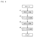
- FIG. 6 is a flowchart showing an example of the atomic layer deposition method of the present embodiment.
- 7A to 7D are diagrams showing a process of forming a thin film on the substrate 100.
- FIG. 6 is a flowchart showing an example of the atomic layer deposition method of the present embodiment.
- 7A to 7D are diagrams showing a process of forming a thin film on the substrate 100.
- the source gas supply unit supplies source gas into the film formation container 11 (step s1). Specifically, the source gas is supplied to the gas introduction unit 20 (step s1). The source gas is supplied into the film forming container 11. The source gas is supplied into the film forming container 11 for 0.1 seconds, for example. As shown in FIG. 7A, in step s1, the source gas 110 is supplied to the inside of the film forming container 11, and the source gas 110 is adsorbed on the substrate 100 to form the adsorption layer 102.
- step s 1 an inert gas is supplied to the inner surface of the injector 21 and the outer surface of the injector deposition preventing material 22. Further, in the discharge unit 30, an inert gas is also supplied to the exhaust flange 31 and the exhaust deposition preventive material 32. Further, an inert gas is also supplied from the upper inert gas supply unit 51 and the lower inert gas supply unit 52 into the film formation container.
- step s1 when supplying the raw material gas, by supplying an inert gas, A gap between the film formation container 11 and the injector 20, A gap between the film forming container 11 and the injector adhesion preventing material 22, A gap between the injector adhesion preventing material 22 and the insulating support 41; A gap between the injector deposition material 22 and the counter electrode deposition material 15; A gap between the film formation container 11 and the exhaust flange 31; A gap between the film formation container 11 and the exhaust gas deposition preventive material 32; A gap between the exhaust gas barrier 32 and the insulating support 41, The gap between the exhaust gas barrier 32 and the counter electrode barrier 15, A gap between the deposition chamber deposition material and the insulating support 41; A gap between the deposition chamber deposition material and the counter electrode deposition material 15; It is possible to suppress the raw material gas from entering.
- step s2 the supply of the source gas is stopped, and the purge gas is supplied at the gas introduction part (step s2).
- the purge gas is supplied into the film forming container 11.
- the source gas is discharged from the exhaust unit 30 to the outside of the film forming container 11.
- the purge gas is supplied into the film forming container 11 for 0.1 seconds, for example.
- the exhaust unit 30 exhausts the source gas 110 and the purge gas 112 inside the film formation container 11.
- the exhaust unit 30 exhausts the source gas 110 and the purge gas 112 inside the film formation container 11 for 2 seconds, for example.
- the purge gas 112 is supplied into the film formation container 11, and the source gas 110 that is not adsorbed on the substrate 100 is purged from the film formation container 11.
- a reactive gas is supplied into the film formation container 11 (step s3).
- the reaction gas is supplied through the gas introduction unit 20 (step s3).
- the reaction gas is supplied to the inside of the film forming container 11 through the passage of the gas introduction unit 20.
- the reaction gas is supplied into the film formation container 11 for 1 second, for example.
- the reaction gas 114 is supplied into the film formation container 11 in step s3.
- step s3 an inert gas is supplied from the inner surface of the injector 21, the outer surface of the injector deposition preventing material 22, and the exhaust part 30. Therefore, in step s3, by supplying an inert gas when supplying the reaction gas into the film formation container 11, A gap between the film formation container 11 and the injector 20, A gap between the film forming container 11 and the injector adhesion preventing material 22, A gap between the injector adhesion preventing material 22 and the insulating support 41; A gap between the injector deposition material 22 and the counter electrode deposition material 15; A gap between the film formation container 11 and the exhaust flange 31; A gap between the film formation container 11 and the exhaust gas deposition preventive material 32; A gap between the exhaust gas barrier 32 and the insulating support 41, The gap between the exhaust gas barrier 32 and the counter electrode barrier 15, A gap between the deposition chamber deposition material and the insulating support 41; A gap between the deposition chamber deposition material and the counter electrode deposition material 15; It is possible to suppress the reaction gas from entering the gas
- step s4 the supply of the reaction gas is stopped, and the purge gas is supplied to the gas introduction unit 20 (step s4).
- the purge gas is supplied into the film forming container 11.
- the purge gas is discharged from the exhaust unit 30 to the outside of the film formation container 11.
- the purge gas is supplied into the film forming container 11 for 0.1 seconds, for example.
- the exhaust unit 30 exhausts the reaction gas 114 and the purge gas 112 inside the film formation container 11.
- step s4 the purge gas 112 is supplied into the film formation container 11 and the reaction gas 114 is purged from the film formation container 11.
- the thin film layer 104 for one atomic layer is formed on the substrate 100. Thereafter, the thin film layer 104 having a desired film thickness can be formed by repeating steps s1 to s4 a predetermined number of times.
- the source gas and the reactive gas are formed in the gap between the film forming container 11 and the injector 21. Can be prevented from entering. Therefore, it is possible to suppress the thin film from adhering to the gap between the film forming container 11 and the injector 21. Similarly, the exhaust portion 30 is also prevented from attaching a thin film. Further, the inert gas is also supplied from the upper inert gas supply unit 51 and the lower inert gas supply unit 52, and film formation inside the film formation container can be suppressed.
- an alumina film formed using TMA as a source gas and O 3 as a reaction gas can be subjected to gas etching using BCl 3 gas.
- gas-etch the alumina film with BCl 3 gas it is necessary to heat it to a high temperature of about 500 ° C., for example.
- the inner wall of the film forming container 11 located in the vicinity of the stage heater 14A can be heated to a high temperature of about 500 ° C. by the stage heater 14A. Therefore, the thin film adhering to the inner wall of the film forming container 11 located in the vicinity of the stage heater 14A can be removed by gas etching.
- TMA trimethylaluminum
- Al source oxygen plasma and nitrogen plasma were used as the reaction gas.
- the film formation was performed in the sequence shown in FIG.
- the pressure inside the film formation container was 100 Pa, and 1000 sccm of nitrogen was supplied from the upper inert gas supply unit and the lower inert gas supply unit, and was constantly supplied during the film formation sequence.
- the portion where the film formation was observed inside the film formation space is an injector, an injector adhesion material, an exhaust adhesion material, a plate electrode adhesion material, two film formation chamber adhesion materials, Only the counter electrode deposition material was used, and no generation of powder was observed. Only the 20 screws used for the above-mentioned anti-adhesive material and the upper electrode anti-adhesive material are the objects of maintenance, and the maintainability is remarkably improved.
Landscapes
- Chemical & Material Sciences (AREA)
- Engineering & Computer Science (AREA)
- Chemical Kinetics & Catalysis (AREA)
- General Chemical & Material Sciences (AREA)
- Materials Engineering (AREA)
- Mechanical Engineering (AREA)
- Metallurgy (AREA)
- Organic Chemistry (AREA)
- Plasma & Fusion (AREA)
- Physics & Mathematics (AREA)
- Analytical Chemistry (AREA)
- Electromagnetism (AREA)
- Inorganic Chemistry (AREA)
- Chemical Vapour Deposition (AREA)
- Drying Of Semiconductors (AREA)
Abstract
ガス導入開口部に成膜容器内側から取り付け可能で、ガス導入開口部の開口を囲む筒状の絶縁性インジェクタ防着材と、排気開口部に成膜容器内側から取り付け可能で、排気開口部の開口を囲む筒状の絶縁性排気防着材と、成膜容器の内壁側に取り付け可能な絶縁性の成膜室防着材を備え、インジェクタ防着材は、平板電極および対向電極側との間に隙間を有し、平板電極端を基準にして、内側に先端が位置し、排気防着材は、平板電極および対向電極側との間に隙間を有し、平板電極端を基準にして、内側に先端が位置し、成膜室防着材は、インジェクタ防着材および排気防着材の両側方にインジェクタ防着材と排気防着材とに亘るように配置され、平板電極および対向電極側との間に隙間を有し、前記隙間から、成膜容器内側に不活性ガスをパージする上部不活性ガス供給口と、前記隙間から成膜容器内側に不活性ガスをパージする下部不活性ガス供給口と、上部不活性ガス供給口に接続される上部不活性ガス供給部と、下部不活性ガス供給口に接続される下部不活性ガス供給部を備える。
Description
本発明は、基板上に薄膜を形成するプラズマ原子層成長装置に関する。
原子層成長法は、形成しようとする薄膜を構成する元素のガスを基板上に交互に供給し、基板上に原子層単位で薄膜を形成するもので、薄膜を均一に形成する技術として知られている。原子層成長法は、一般的なCVD(Chemical Vapor Deposition)法と比較して、段差被覆性や膜厚制御性に優れている。
原子層成長法により薄膜の形成を繰り返し行うと、成膜容器の内表面にも薄膜が付着する。成膜容器内表面に付着した薄膜の厚さが厚くなると、堆積した薄膜が剥離し、その一部分がパーティクルとなり、基板上に形成される薄膜の質が劣化する原因となる。そのため、成膜容器の内表面に付着した薄膜を定期的に除去することが好ましい。
原子層成長法により薄膜の形成を繰り返し行うと、成膜容器の内表面にも薄膜が付着する。成膜容器内表面に付着した薄膜の厚さが厚くなると、堆積した薄膜が剥離し、その一部分がパーティクルとなり、基板上に形成される薄膜の質が劣化する原因となる。そのため、成膜容器の内表面に付着した薄膜を定期的に除去することが好ましい。
特許文献1では、CVD成膜やスパッタ成膜などの気相成長装置において、防着板を使用するとともに、さらに、チャンバの内壁に堆積した堆積物を非晶質膜で覆う処理方法および装置が提案されている。従来の気相成長装置では、係る手段によりクリーニングの頻度を低減することは可能であるが、チャンバの内壁に堆積した堆積物や堆積物を覆う非晶質膜の厚さが所定の厚さ以上になった場合、ウェットエッチング方法を用いてクリーニングを行う必要がある。しかし、ウェットエッチング方法では、成膜容器を開放するため、成膜容器が大型になるにつれて、開放作業の手間が大きくなるため、ガスエッチング方法を用いることができる場合は、ガスエッチング方法を用いることが好ましい。ガスエッチング方法によりエッチングを行うためには、成膜容器の内壁面の薄膜の付着部分を所定の温度以上に加熱する必要があるが、ヒーターから離れた部分では、必要な加熱温度に達せず、ガスエッチングを行うのが困難になる。そのため、ガスエッチングを行いにくい場所にある程度の量の薄膜が付着した場合、成膜容器を開放してウェットエッチングを行う必要が生じる。
ウェットエッチング周期を長くし、さらに成膜容器本体へ着膜を抑制することを目的として、成膜容器内に防着板を挿入する手法が提案されている(特許文献2参照)。従来の方式では、防着板を分割し成膜容器内に設置する。防着板を分割することで、取り扱いが容易となり、さらに高温に加熱する装置である場合は、分割された防着板の隙間に空間を設けることで、防着板の熱膨張を吸収することが可能となる。
しかし、原子層成長装置では、原料ガス及び反応ガス微細に隙間へ容易に侵入し、膜を形成する。このような微細な隙間に侵入したガスは、膜及び粉となり、パーティクルの要因となる。よって、原子層成長装置においては、防着板の分割を可能な限り抑制することが好ましい。
しかし、原子層成長装置では、原料ガス及び反応ガス微細に隙間へ容易に侵入し、膜を形成する。このような微細な隙間に侵入したガスは、膜及び粉となり、パーティクルの要因となる。よって、原子層成長装置においては、防着板の分割を可能な限り抑制することが好ましい。
防着板の分割が必要な場合において着膜を抑制させるには、例えば特許文献3で示されるように、不活性ガスを供給する手法を用いることができる。
また、プラズマを使用しない原子層成長成膜においては、特許文献4に示される防着板を利用することで基板上部を保護することが可能である。一方、基板の上部に高周波を印加する電極が設置される平行平板型のプラズマ装置においては、高周波が印加される電極を支持するために絶縁体を用いる。この絶縁体には主にテフロン(登録商標)のような樹脂やセラミックスを利用する。
また、プラズマを使用しない原子層成長成膜においては、特許文献4に示される防着板を利用することで基板上部を保護することが可能である。一方、基板の上部に高周波を印加する電極が設置される平行平板型のプラズマ装置においては、高周波が印加される電極を支持するために絶縁体を用いる。この絶縁体には主にテフロン(登録商標)のような樹脂やセラミックスを利用する。
しかし、上部電極を固定する絶縁支持体は、ウェットエッチングで再生可能であるが、支持体を分解し、平板電極を再構築することで、平板電極の取り付け位置が以前の取り付け位置と変わり、プラズマ状態がメンテナンス前と変化するおそれがある。よって、絶縁支持体のメンテナンスは好ましくなく、メンテナンスフリーであることが好ましい。
そこで、絶縁支持体に絶縁防着板を利用することが考えられる。その際には、絶縁防着板をビスなどの固定手段で固定する。しかし、原子層成長では、例えばビス穴などにも容易に着膜が生じるため、膜の力でビスが強固に固定される。よって、着膜がなされると、ビスの取り外しには大きな力が必要とされるが、その際、ビスおよび防着板がセラミックス製であると破壊されやすい。樹脂は変形の危険があるため使用は困難である。
よって、絶縁支持体のメンテナンスは、防着板を使用しようとしても煩雑となるため、この部分には一切の着膜を抑制することが好ましい。
そこで、絶縁支持体に絶縁防着板を利用することが考えられる。その際には、絶縁防着板をビスなどの固定手段で固定する。しかし、原子層成長では、例えばビス穴などにも容易に着膜が生じるため、膜の力でビスが強固に固定される。よって、着膜がなされると、ビスの取り外しには大きな力が必要とされるが、その際、ビスおよび防着板がセラミックス製であると破壊されやすい。樹脂は変形の危険があるため使用は困難である。
よって、絶縁支持体のメンテナンスは、防着板を使用しようとしても煩雑となるため、この部分には一切の着膜を抑制することが好ましい。
本発明は、成膜容器および成膜容器内部の防着材のクリーニングの頻度を低減し、メンテナンスパーツ数を低減し、メンテナンス作業性を向上させることができるプラズマ原子層成長装置を提供することを目的とする。
すなわち、本発明のプラズマ原子層成長装置のうち、第1の形態は、
成膜容器と、
前記成膜容器内に保持された基板と対向するように設けられた平板電極と、
前記成膜容器内部で基板を保持する対向電極と、
前記成膜容器の一側壁部に設けられたガス導入開口部と、前記一側壁部に対向する前記成膜容器の他側壁部に設けられた排気開口部と、を備え、
前記基板上に薄膜を形成するプラズマ原子層成長装置であって、
前記ガス導入開口部に前記成膜容器内側から取り付け可能で、前記ガス導入開口部の開口を囲むように筒状に配置された絶縁性のインジェクタ防着材と、
前記排気開口部に前記成膜容器内側から取り付け可能で、前記排気開口部の開口を囲むように筒状に配置された絶縁性の排気防着材と、
前記成膜容器の内壁側に取り付け可能な絶縁性の成膜室防着材と、を備え、
前記インジェクタ防着材は、
前記平板電極および前記対向電極側との間に隙間を有し、かつ、前記ガス導入開口部側の前記平板電極端を基準にして、内側に先端が位置し、
前記排気防着材は、
前記平板電極および前記対向電極側との間に隙間を有し、かつ、前記排気開口部側の前記平板電極端を基準にして、内側に先端が位置し、
前記成膜室防着材は、
少なくとも前記インジェクタ防着材および前記排気防着材の両側方に位置して、前記平板電極および前記対向電極側との間に隙間を有し、
さらに、前記平板電極と、前記インジェクタ防着材、前記排気防着材および前記成膜室防着材との間の前記隙間から、前記成膜容器の内側に向けて不活性ガスをパージする上部不活性ガス供給口と、
前記対向電極と、前記インジェクタ防着材、前記排気防着材および前記成膜室防着材との間の前記隙間から前記成膜容器の内側に向けて不活性ガスをパージする下部不活性ガス供給口と、
前記上部不活性ガス供給口に接続される上部不活性ガス供給部と、
前記下部不活性ガス供給口に接続される下部不活性ガス供給部と、
を備えることを特徴とする。
成膜容器と、
前記成膜容器内に保持された基板と対向するように設けられた平板電極と、
前記成膜容器内部で基板を保持する対向電極と、
前記成膜容器の一側壁部に設けられたガス導入開口部と、前記一側壁部に対向する前記成膜容器の他側壁部に設けられた排気開口部と、を備え、
前記基板上に薄膜を形成するプラズマ原子層成長装置であって、
前記ガス導入開口部に前記成膜容器内側から取り付け可能で、前記ガス導入開口部の開口を囲むように筒状に配置された絶縁性のインジェクタ防着材と、
前記排気開口部に前記成膜容器内側から取り付け可能で、前記排気開口部の開口を囲むように筒状に配置された絶縁性の排気防着材と、
前記成膜容器の内壁側に取り付け可能な絶縁性の成膜室防着材と、を備え、
前記インジェクタ防着材は、
前記平板電極および前記対向電極側との間に隙間を有し、かつ、前記ガス導入開口部側の前記平板電極端を基準にして、内側に先端が位置し、
前記排気防着材は、
前記平板電極および前記対向電極側との間に隙間を有し、かつ、前記排気開口部側の前記平板電極端を基準にして、内側に先端が位置し、
前記成膜室防着材は、
少なくとも前記インジェクタ防着材および前記排気防着材の両側方に位置して、前記平板電極および前記対向電極側との間に隙間を有し、
さらに、前記平板電極と、前記インジェクタ防着材、前記排気防着材および前記成膜室防着材との間の前記隙間から、前記成膜容器の内側に向けて不活性ガスをパージする上部不活性ガス供給口と、
前記対向電極と、前記インジェクタ防着材、前記排気防着材および前記成膜室防着材との間の前記隙間から前記成膜容器の内側に向けて不活性ガスをパージする下部不活性ガス供給口と、
前記上部不活性ガス供給口に接続される上部不活性ガス供給部と、
前記下部不活性ガス供給口に接続される下部不活性ガス供給部と、
を備えることを特徴とする。
他の形態のプラズマ原子層成長装置の発明は、前記形態の本発明において、
前記インジェクタ防着材は、
前記ガス導入開口部側の前記平板電極端を基準にして、前記平板電極端から前記平板電極中央方向に、先端位置が0.1mm以上、200mm以下の範囲で位置するように伸長し、
前記排気防着材は、
前記排気開口部側の前記平板電極端を基準にして、前記平板電極端から前記平板電極中央方向に、先端位置が0.1mm以上、200mm以下の範囲で位置するように伸長していることを特徴とする。
前記インジェクタ防着材は、
前記ガス導入開口部側の前記平板電極端を基準にして、前記平板電極端から前記平板電極中央方向に、先端位置が0.1mm以上、200mm以下の範囲で位置するように伸長し、
前記排気防着材は、
前記排気開口部側の前記平板電極端を基準にして、前記平板電極端から前記平板電極中央方向に、先端位置が0.1mm以上、200mm以下の範囲で位置するように伸長していることを特徴とする。
他の形態のプラズマ原子層成長装置の発明は、前記形態の本発明において、
前記インジェクタ防着材による筒状の開口部の側端部は、前記対向電極に保持された基板の側方側の端部から外側に0.1mm以上200mm以下の距離を有し、
前記排気防着材による筒状の開口部の側端部は、前記対向電極に保持された基板の側方側の端部から外側に0.1mm以上200mm以下の距離を有することを特徴とする。
前記インジェクタ防着材による筒状の開口部の側端部は、前記対向電極に保持された基板の側方側の端部から外側に0.1mm以上200mm以下の距離を有し、
前記排気防着材による筒状の開口部の側端部は、前記対向電極に保持された基板の側方側の端部から外側に0.1mm以上200mm以下の距離を有することを特徴とする。
他の形態のプラズマ原子層成長装置の発明は、前記形態の本発明において、
前記成膜室防着材は、前記インジェクタ防着材の側部および前記排気防着材の側部の上下幅を覆う大きさを有し、かつ、前記成膜室防着材の内側面と前記インジェクタ防着材の外側面とが0.1mm以上20mm以下の水平距離の隙間を有し、前記成膜室防着材の内側面と前記排気防着材の外側面とが0.1mm以上20mm以下の水平距離の隙間を有することを特徴とする請求項1または2に記載のプラズマ原子層成長装置。
前記成膜室防着材は、前記インジェクタ防着材の側部および前記排気防着材の側部の上下幅を覆う大きさを有し、かつ、前記成膜室防着材の内側面と前記インジェクタ防着材の外側面とが0.1mm以上20mm以下の水平距離の隙間を有し、前記成膜室防着材の内側面と前記排気防着材の外側面とが0.1mm以上20mm以下の水平距離の隙間を有することを特徴とする請求項1または2に記載のプラズマ原子層成長装置。
他の形態のプラズマ原子層成長装置の発明は、前記形態の本発明において、
前記成膜室防着材と前記インジェクタ防着材とは、前記ガス導入開口部と前記排気開口部との間のガスの流れ方向で、0.1mm以上200mm以下の重なりを有し、
前記成膜室防着材と前記排気防着材とは、前記ガス導入開口部と前記排気開口部との間のガスの流れ方向で、0.1mm以上200mm以下の重なりを有することを特徴とする。
前記成膜室防着材と前記インジェクタ防着材とは、前記ガス導入開口部と前記排気開口部との間のガスの流れ方向で、0.1mm以上200mm以下の重なりを有し、
前記成膜室防着材と前記排気防着材とは、前記ガス導入開口部と前記排気開口部との間のガスの流れ方向で、0.1mm以上200mm以下の重なりを有することを特徴とする。
他の形態のプラズマ原子層成長装置の発明は、前記形態の本発明において、
前記インジェクタ防着材は、側方外面が、前記平板電極の側端を基準にして、0.1mm以上、200mm以下の距離で内側に位置し、
前記排気防着材は、側方外面が、前記平板電極端の側端を基準にして、0.1mm以上、200mm以下の距離で内側に位置していることを特徴とする。
前記インジェクタ防着材は、側方外面が、前記平板電極の側端を基準にして、0.1mm以上、200mm以下の距離で内側に位置し、
前記排気防着材は、側方外面が、前記平板電極端の側端を基準にして、0.1mm以上、200mm以下の距離で内側に位置していることを特徴とする。
他の形態のプラズマ原子層成長装置の発明は、前記形態の本発明において、
前記成膜室防着材、インジェクタ防着材および排気防着材は、近接する平板電極端から50mm以上離れた距離の位置に前記成膜容器に対する固定端部を有するように前記成膜容器に取り付け固定されていることを特徴とする。
前記成膜室防着材、インジェクタ防着材および排気防着材は、近接する平板電極端から50mm以上離れた距離の位置に前記成膜容器に対する固定端部を有するように前記成膜容器に取り付け固定されていることを特徴とする。
他の形態のプラズマ原子層成長装置の発明は、前記形態の本発明において、前記成膜室防着材が、前記インジェクタ防着材と前記排気防着材とに亘る長さを有することを特徴とする。
他の形態のプラズマ原子層成長装置の発明は、前記形態の本発明において、
前記上部不活性ガス供給部および前記下部不活性ガス供給部は、それぞれシャワーヘッド構造によって前記上部不活性ガス供給口および前記下部不活性ガス供給口に接続されていることを特徴とする。
前記上部不活性ガス供給部および前記下部不活性ガス供給部は、それぞれシャワーヘッド構造によって前記上部不活性ガス供給口および前記下部不活性ガス供給口に接続されていることを特徴とする。
他の形態のプラズマ原子層成長装置の発明は、前記形態の本発明において、
前記インジェクタ防着材上面および排気防着材上面と、前記平板電極側下面とが、0.1mm以上20mm以下の垂直距離の隙間を有していることを特徴とする。
前記インジェクタ防着材上面および排気防着材上面と、前記平板電極側下面とが、0.1mm以上20mm以下の垂直距離の隙間を有していることを特徴とする。
他の形態のプラズマ原子層成長装置の発明は、前記形態の本発明において、
前記インジェクタ防着材および前記排気防着材は、前記ガス導入部と前記排気部との間のガスの流れ方向において、前記対向電極に保持された基板の近接する端部と、水平距離で0.1mm以上、200mm以下の隙間を有していることを特徴とする。
前記インジェクタ防着材および前記排気防着材は、前記ガス導入部と前記排気部との間のガスの流れ方向において、前記対向電極に保持された基板の近接する端部と、水平距離で0.1mm以上、200mm以下の隙間を有していることを特徴とする。
他の形態のプラズマ原子層成長装置の発明は、前記形態の本発明において、
前記インジェクタ防着材下面および排気防着材下面と、前記対向電極側上面とが、0.1mm以上20mm以下の垂直距離の隙間を有していることを特徴とする。
前記インジェクタ防着材下面および排気防着材下面と、前記対向電極側上面とが、0.1mm以上20mm以下の垂直距離の隙間を有していることを特徴とする。
他の形態のプラズマ原子層成長装置の発明は、前記形態の本発明において、
前記対向電極は、基板を保持する保持面を有する対向電極保持部と、対向電極保持部の周囲にあって、前記対向電極保持面よりも低い高さを有する対向電極周縁部と、を有することを特徴とする。
前記対向電極は、基板を保持する保持面を有する対向電極保持部と、対向電極保持部の周囲にあって、前記対向電極保持面よりも低い高さを有する対向電極周縁部と、を有することを特徴とする。
本発明によれば、成膜容器内部の着膜面積を低減でき、パーティクル発生の抑制と成膜容器及び防着材のクリーニング頻度低減が可能となる。
まず、添付図面を参照して、本実施形態のプラズマ原子層成長装置10の構成を説明する。
図1は、本実施形態のプラズマ原子層成長装置の一例を示す概略構成図である。
本実施形態のプラズマ原子層成長装置10は、原料ガスと反応ガスとを交互に供給し、基板100上に原子層単位で薄膜を形成する。その際、反応活性を高めるため、基板100を加熱させることができる。本実施形態では原料ガスとしてTMA(Tri-Methyl-Aluminum)を用い、その際、反応活性を高めるため、プラズマを発生させる。本実施形態では、プラズマの発生に平行平板電極を用いる。
図1は、本実施形態のプラズマ原子層成長装置の一例を示す概略構成図である。
本実施形態のプラズマ原子層成長装置10は、原料ガスと反応ガスとを交互に供給し、基板100上に原子層単位で薄膜を形成する。その際、反応活性を高めるため、基板100を加熱させることができる。本実施形態では原料ガスとしてTMA(Tri-Methyl-Aluminum)を用い、その際、反応活性を高めるため、プラズマを発生させる。本実施形態では、プラズマの発生に平行平板電極を用いる。
成膜容器11は、インジェクタ21と排気フランジ31と、平板電極12と、対向電極14と、高周波電源16と、を備える。対向電極14はステージヒーター14Aを備え、基板100の温度を調整することができる。例えば、プラズマ原子層成長装置の場合、基板100を50~200℃に加熱する。成膜容器11は、処理に際し、真空に維持される。
平板電極12は、成膜空間Sを隔て基板100の上方に設けられ、絶縁支持体41により支持されている。絶縁支持体41で露出する面が平板電極12として機能し、露出している面の端部が平板電極12の端部に相当する。平板電極12の露出している下面側には、導電性の板状の平板電極防着材13が設けられており、平板電極防着材13の下面と絶縁支持体41の下面とが面一になっている。
また、対向電極14は、基板100が保持される保持面を有する対向電極保持部14Bの周囲に、保持面よりも高さが低くなった対向電極周縁部14Cを有しており、対向電極周縁部14Cにおいてステージストッパ17で成膜容器11に保持されている。また、対向電極周縁部14Cの上面および保持面との境の縦面に板状の対向電極防着材15が設けられている。
高周波電源16が所定の周波数の高周波電流を平板電極12に供給することにより、平板電極12と対向電極14との間でプラズマが生成される。
また、対向電極14は、基板100が保持される保持面を有する対向電極保持部14Bの周囲に、保持面よりも高さが低くなった対向電極周縁部14Cを有しており、対向電極周縁部14Cにおいてステージストッパ17で成膜容器11に保持されている。また、対向電極周縁部14Cの上面および保持面との境の縦面に板状の対向電極防着材15が設けられている。
高周波電源16が所定の周波数の高周波電流を平板電極12に供給することにより、平板電極12と対向電極14との間でプラズマが生成される。
次に、原料ガス、反応ガス、パージガスが導入されるガス導入部20について説明する。ガス導入部20は、原料ガス、反応ガス、パージガスを、処理過程に従って成膜容器11内に供給する。インジェクタ21は成膜容器11のガス導入開口部11Aに取り付けられ、ガス導入開口部11Aに、成膜容器11の内側からインジェクタ防着材22が挿入されてガス導入開口部11Aの開口を囲むように取り付けられる。インジェクタ防着材は、前記開口を挿入して囲むか、外側から囲むか、またはこれらが組み合わされた、いずれの構成でもよい。
なお、この例では、ガス導入開口部11Aは、角穴形状に形成され、ガス導入開口部11Aを囲むように、角筒状にインジェクタ防着材22が配置されている。インジェクタ防着材22は、筒形状に形成されているものでもよく、複数の部材が接合されて筒状とされているものであってもよい。インジェクタ防着材は、前記開口部に挿入して開口を囲むか、外側から開口を囲むか、またはこれらが組み合わされた、いずれの構成でもよい。
なお、この例では、ガス導入開口部11Aは、角穴形状に形成され、ガス導入開口部11Aを囲むように、角筒状にインジェクタ防着材22が配置されている。インジェクタ防着材22は、筒形状に形成されているものでもよく、複数の部材が接合されて筒状とされているものであってもよい。インジェクタ防着材は、前記開口部に挿入して開口を囲むか、外側から開口を囲むか、またはこれらが組み合わされた、いずれの構成でもよい。
次に、排気部30について説明する。排気部30は、原料ガス、反応ガス、パージガスを、処理過程に従って成膜容器11から排気する。排気フランジ31は成膜容器11の排気開口部11Bに取り付けられ、排気開口部11Bに成膜容器11の内側から排気防着材32が挿入されて排気開口部11Bの開口を囲むように取り付けられる。排気防着材は、前記開口部に挿入して開口を囲むか、外側から開口を囲むか、またはこれらが組み合わされた、いずれの構成でもよい。
なお、この例では、排気開口部11Bは、角穴形状に形成され、排気開口部11Bを囲むように、角筒状に排気防着材32が配置されている。排気防着材32は、筒形状に形成されているものでもよく、複数の部材が接合されて筒状とされているものであってもよい。排気防着材32は、排気開口部11Bの形状に合わせた筒形状にすることができる。
成膜容器11に導入されたガスは、処理過程に従ってガス導入部20から排気部30に向けてガスの流れが生じる。このガスの流れ方向と交差する方向を以下では側方として説明する。
なお、この例では、排気開口部11Bは、角穴形状に形成され、排気開口部11Bを囲むように、角筒状に排気防着材32が配置されている。排気防着材32は、筒形状に形成されているものでもよく、複数の部材が接合されて筒状とされているものであってもよい。排気防着材32は、排気開口部11Bの形状に合わせた筒形状にすることができる。
成膜容器11に導入されたガスは、処理過程に従ってガス導入部20から排気部30に向けてガスの流れが生じる。このガスの流れ方向と交差する方向を以下では側方として説明する。
図2は、ガス導入部20から排気部30に向けたガス流れ方向に平行な成膜容器11側面から見た場合のガス導入部20周辺の拡大断面図である。
絶縁体のインジェクタ防着材22は、成膜容器11内側から挿入されて取り付けられており、固定ビス23で成膜容器11に固定されている。
インジェクタ防着材22の上側に当たるインジェクタ防着材上部板22Aは、平板電極12側に設けられた平板電極防着材13との間に、垂直方向に隙間を有し、インジェクタ防着材22の下側に当たるインジェクタ防着材下部板22Bは、対向電極14側の対向電極防着材15との間に、垂直方向に隙間を有している。
絶縁体のインジェクタ防着材22は、成膜容器11内側から挿入されて取り付けられており、固定ビス23で成膜容器11に固定されている。
インジェクタ防着材22の上側に当たるインジェクタ防着材上部板22Aは、平板電極12側に設けられた平板電極防着材13との間に、垂直方向に隙間を有し、インジェクタ防着材22の下側に当たるインジェクタ防着材下部板22Bは、対向電極14側の対向電極防着材15との間に、垂直方向に隙間を有している。
また、インジェクタ防着材22と排気防着材32の両側方には、成膜室防着材63が配置されて成膜容器11の内壁に取り付けられて固定されている。この例では、成膜容器11の内壁から張り出した張り出し壁64上に設置され、かつ固定ビス65で張り出し壁64に固定されている。成膜室防着材63は、インジェクタ防着材22のインジェクタ防着材側部板22Cの上下幅を覆う大きさを有しており、さらに、インジェクタ防着材側部板22Cと排気防着材側部板32Cとに亘る長さを有している。
成膜室防着材63の内面は、インジェクタ防着材側部板22Cの外面および排気防着材側部板32Cの外面と隙間を有し、さらに、成膜室防着材63は、絶縁支持体41、平板電極防着材13、対向電極防着材15および、対向電極14に保持された基板100とは隙間を有している。
インジェクタ防着材22、排気防着材32、成膜室防着材63の内側の空間は、成膜空間Sを構成する。
成膜室防着材63の内面は、インジェクタ防着材側部板22Cの外面および排気防着材側部板32Cの外面と隙間を有し、さらに、成膜室防着材63は、絶縁支持体41、平板電極防着材13、対向電極防着材15および、対向電極14に保持された基板100とは隙間を有している。
インジェクタ防着材22、排気防着材32、成膜室防着材63の内側の空間は、成膜空間Sを構成する。
成膜容器11には、上部不活性ガス供給部51と下部不活性ガス供給部52が接続されており、上部不活性ガス供給部51は、成膜容器11内側に設けられた上部不活性ガス供給口53に接続され、下部不活性ガス供給部52は、成膜容器11内側に設けられた下部不活性ガス供給口54に接続されている。上部不活性ガス供給部51および下部不活性ガス供給部52は、例えば窒素などの不活性ガスを供給することができる。
インジェクタ防着材上部板22Aと、絶縁支持体41、平板電極12および平板電極防着材13によってできた隙間を通して、上部不活性ガス供給口53から吹き出される不活性ガスが成膜容器11内へ供給される。
また、排気防着材上部板32Aと、絶縁支持体41、平板電極12および平板電極防着材13によってできた隙間を通して、上部不活性ガス供給口53から吹き出される不活性ガスが成膜容器11内へ供給される。
さらに、成膜室防着材63と、絶縁支持体41、平板電極12および平板電極防着材13によってできた隙間を通して、上部不活性ガス供給口53から吹き出される不活性ガスが成膜容器11内へ供給される。
また、排気防着材上部板32Aと、絶縁支持体41、平板電極12および平板電極防着材13によってできた隙間を通して、上部不活性ガス供給口53から吹き出される不活性ガスが成膜容器11内へ供給される。
さらに、成膜室防着材63と、絶縁支持体41、平板電極12および平板電極防着材13によってできた隙間を通して、上部不活性ガス供給口53から吹き出される不活性ガスが成膜容器11内へ供給される。
インジェクタ防着材下部板22Bと、対向電極14、対向電極防着材15、対向電極14に保持された基板100によってできた隙間を通して、下部不活性ガス供給口54から吹き出される不活性ガスが成膜容器11内へ供給される。
また、排気防着材下部板32Bと、対向電極14、対向電極防着材15、対向電極14に保持された基板100によってできた隙間を通して、下部不活性ガス供給口54から吹き出される不活性ガスが成膜容器11内へ供給される。
さらに、成膜室防着材63と、対向電極14、対向電極防着材15、対向電極14に保持された基板100によってできた隙間を通して、下部不活性ガス供給口54から吹き出される不活性ガスが成膜容器11内へ供給される。
また、排気防着材下部板32Bと、対向電極14、対向電極防着材15、対向電極14に保持された基板100によってできた隙間を通して、下部不活性ガス供給口54から吹き出される不活性ガスが成膜容器11内へ供給される。
さらに、成膜室防着材63と、対向電極14、対向電極防着材15、対向電極14に保持された基板100によってできた隙間を通して、下部不活性ガス供給口54から吹き出される不活性ガスが成膜容器11内へ供給される。
ここで、インジェクタ防着材22は、インジェクタ防着材上部板22Aの先端が、平板電極12の端部から内側に位置しており、さらには、平板電極12の前記端部を基準にして、平板電極中央方向に、0.1mm以上、200mm以下の水平距離aで伸長していることが好ましい。水平距離aの値が大きいことで、原料ガスおよび反応ガスが、インジェクタ防着材22の出口から上部不活性ガス供給口53側へ侵入することを抑制することが可能である。しかし、水平距離aの値が大きいと成膜容器11が大きくなるため、最適値が必要となる。本原子層成長装置においては、上限が20mmであることが好ましい。
また、図2に示すように、平板電極12下面側とインジェクタ防着材22のインジェクタ防着材上部板22A上面とは隙間を有しており、さらには、0.1mm以上20mm以下の垂直距離bを有することが好ましい。なお、平板電極12に平板電極防着材13を利用する場合は、平板電極防着材13とインジェクタ防着材上面の垂直距離がbとなる。
垂直距離bの値が小さいことで、原料ガスおよび反応ガスが上部不活性ガス供給口53側へ侵入することを抑制することが可能である。しかし、垂直距離bの値が極端に小さいと、成膜容器11の加工精度によりインジェクタ防着材22と絶縁支持体41が干渉し、破損する可能性がある。垂直距離bの値が大きいと、原料ガスおよび反応ガスが、インジェクタ防着材22出口から上部不活性ガス供給口53側へ侵入するため、最適値が必要となる。本原子層成長装置においては、上限は3mmであることが好ましい。
垂直距離bの値が小さいことで、原料ガスおよび反応ガスが上部不活性ガス供給口53側へ侵入することを抑制することが可能である。しかし、垂直距離bの値が極端に小さいと、成膜容器11の加工精度によりインジェクタ防着材22と絶縁支持体41が干渉し、破損する可能性がある。垂直距離bの値が大きいと、原料ガスおよび反応ガスが、インジェクタ防着材22出口から上部不活性ガス供給口53側へ侵入するため、最適値が必要となる。本原子層成長装置においては、上限は3mmであることが好ましい。
また、インジェクタ防着材22は、絶縁体である必要がある。金属である場合は、平板電極12とインジェクタ防着材22との間で放電を起こすからである。例えば、インジェクタ防着材22をアルミナセラミックスで作製することで、放電を抑制することができる。
また、インジェクタ防着材22は、図2に示すように、インジェクタ防着材下部板22Bの先端が、対向電極14に保持された基板100の端部と隙間を有しており、さらには前記隙間の水平距離cは、0.1mm以上、200mm以下であることが好ましい。水平距離cの値が小さいことで、原料ガスおよび反応ガスが下部不活性ガス供給口54側へ侵入することを抑制することが可能である。水平距離cが、極端に小さい場合は、インジェクタ防着材22と基板100と干渉する可能性がある。しかし、基板100上にマスクを有する成膜においては、マスクを設置するスペースが必要となる。よって、cの値は、本原子層成長装置においては、マスク成膜に対応可能な100mmとすることが好ましい。
また、図2で示すように、インジェクタ防着材22のインジェクタ防着材下部板22Bの下面と、対向電極14上面側とは、隙間を有しており、さらには、前記隙間の垂直距離dは、0.1mm以上20mm以下であることが好ましく、さらには3mmであることが一層好ましい。垂直距離dの値が小さいことで、原料ガスおよび反応ガスが下部不活性ガス供給口54側へ侵入することを抑制することが可能である。しかし、垂直距離dの値が極端に小さいと、成膜容器11の加工精度によりインジェクタ防着材22と対向電極14とが干渉し、破損する可能性があるため、最適値が必要となる。また、対向電極14上には対向電極防着材15を使用してもよい。この場合は、対向電極防着材15上面とインジェクタ防着材22下面の距離がdとなる。
また、インジェクタ防着材22は、図2に示すように、平板電極12の端面から50mm以上の水平距離eを有した地点で固定されることが好ましい。この例では、固定には固定ビス23を用いているが、金属製のビスを用いると異常放電を生じやすいため、平板電極12と距離を設ける必要がある。樹脂製のビスを用いる場合は、異常放電を抑制することが可能であるが、プラズマに曝されると、樹脂が変形することがあり、デガスを生じることもあるため、やはり、平板電極からの距離を大きくする必要がある。また、原料ガスおよび反応ガスは、ビス穴へ容易に侵入し、着膜やパウダー発生要因となる。よって、原料ガスおよび反応ガスに曝露される位置に設置するのは好ましくない。なお、固定方法が固定ビスに限定されるものではない。
排気部30については、ガス導入部20と全く同様のことがいえる。ガス導入部20と排気部30は対称であることが好ましい。したがって、排気防着材32においても、前記した距離a~eにおける上記条件を同様に満たすのが望ましい。この場合、インジェクタ防着材22を排気防着材32に置き換えて同条件が示される。
図3は、成膜室排気側から見た場合のガス導入部周辺の拡大図である。図3に示すように、インジェクタ防着材22の開口部内面22C0と基板100の端部との距離fは、0.1mm以上200mm以下であることが好ましい。距離が小さいと、側壁でガス流れが乱れるため、良好な膜厚及び膜質の均一性を得ることができないが、逆に大きすぎる場合は消費原料が増大し、ランニングコストが増大する。また、ガラス基板上にマスクを有する成膜においては、マスクを収納するスペースが必要となる。よって、距離fの値はマスク成膜に対応可能な100mmとすることが好ましい。排気部30についても、原料ガス、反応ガスパージガスを導入するガス導入部20と全く同様のことがいえる。導入部20と排気部30は対称であることが好ましい。したがって、排気部30においても距離fの値を満たすのが望ましい。
平板電極12側方端と成膜室防着材63の内側面との関係では、平板電極12の側方端よりも内側に成膜室防着材63の内側面が位置しているのが望ましく、その際の水平距離jは、0.1mm以上200mm以下が好ましい。jの値が大きいことで、原料ガスおよび反応ガスが、成膜室防着材63側へ侵入することを抑制することが可能である。しかし、値が大きいと成膜容器が大きくなるため、最適値が必要となる。本原子層成長装置においては20mmであることが好ましい。
また、成膜室防着材63の固定は、図3で示すように、固定ビス23と同等の理由で、平板電極12の端面から50mm以上の水平距離gを有した地点で固定されることが好ましい。
また、成膜室防着材63の固定は、図3で示すように、固定ビス23と同等の理由で、平板電極12の端面から50mm以上の水平距離gを有した地点で固定されることが好ましい。
また図4は、成膜容器内部の防着材の配置図である。インジェクタ防着材22と排気防着材32は、成膜室防着材63によって図4のように囲まれることが好ましい。インジェクタ防着材22外面および排気防着材32外面と、成膜室防着材63の内面との水平距離hは、0.1mm以上20mm以下であることが好ましく、さらには1mmであることが好ましい。hの値が小さいことで、原料ガスおよび反応ガスが成膜容器11内壁側へ侵入することを抑制することが可能である。ただし、値が極端に小さい場合は、インジェクタ防着材22および成膜室防着材63が熱膨張を起こし、干渉、破壊するため好ましくない。
また、インジェクタ防着材22と成膜室防着材63とのガスの流れ方向における重なり距離iは、0.1mm以上200mm以下であることが好ましく、さらには重なり部分から固定ビス23までの距離を120mmとするのが好ましい。距離iの値が大きいことで、原料ガスおよび反応ガスが成膜容器11内壁側へ侵入することを抑制することが可能である。
排気防着材33についても、インジェクタ防着材22と全く同様のことがいえる。したがって、排気防着材33においても、距離f~jが上記各条件を満たすのが望ましい。この場合、インジェクタ防着材22を排気防着材32に置き換えて同条件が示される。
また、インジェクタ防着材22と成膜室防着材63とのガスの流れ方向における重なり距離iは、0.1mm以上200mm以下であることが好ましく、さらには重なり部分から固定ビス23までの距離を120mmとするのが好ましい。距離iの値が大きいことで、原料ガスおよび反応ガスが成膜容器11内壁側へ侵入することを抑制することが可能である。
排気防着材33についても、インジェクタ防着材22と全く同様のことがいえる。したがって、排気防着材33においても、距離f~jが上記各条件を満たすのが望ましい。この場合、インジェクタ防着材22を排気防着材32に置き換えて同条件が示される。
図5は成膜容器を上面から見た上部不活性ガス供給部51および上部不活性ガス供給口53を示す概略図である。成膜容器11に貫通穴を設け、成膜容器11全周からシャワー供給することが好ましい。図5では上部不活性ガス供給部51を4か所設けているが、1か所でもよい。上部不活性ガス供給部51は、シャワーヘッド構造によって上部不活性ガス供給口53に接続されている。
また、下部不活性ガス供給部52は、上部不活性ガス供給部51と同等の構造としてもよく、さらには、供給部を1つとし、その後、上部不活性ガス供給口、下部不活性ガス供給部口へ分岐される構造としてもよい。各供給口におけるシャワー穴径は1~3mm径の範囲内であることが好ましく、1mm程度でよい。シャワー穴ピッチは10mm~200mmピッチであることが好ましい。成膜容器11に貫通穴を設けてシャワーを作製してもよく、シャワープレートを個別に作製し、成膜容器11に取り付けてもよい。
また、下部不活性ガス供給部52は、上部不活性ガス供給部51と同等の構造としてもよく、さらには、供給部を1つとし、その後、上部不活性ガス供給口、下部不活性ガス供給部口へ分岐される構造としてもよい。各供給口におけるシャワー穴径は1~3mm径の範囲内であることが好ましく、1mm程度でよい。シャワー穴ピッチは10mm~200mmピッチであることが好ましい。成膜容器11に貫通穴を設けてシャワーを作製してもよく、シャワープレートを個別に作製し、成膜容器11に取り付けてもよい。
次に、プラズマ原子層成長装置10における処理手順を説明する。
図6は、本実施形態の原子層堆積方法の一例を示すフローチャートである。図7A~Dは、基板100の上に薄膜が形成される工程を示す図である。
図6は、本実施形態の原子層堆積方法の一例を示すフローチャートである。図7A~Dは、基板100の上に薄膜が形成される工程を示す図である。
まず、原料ガス供給部が成膜容器11の内部に原料ガスを供給する(ステップs1)。具体的には、ガス導入部20に原料ガスを供給する(ステップs1)。原料ガスは、成膜容器11の内部に供給される。原料ガスは、例えば、0.1秒間、成膜容器11の内部に供給する。図7Aに示されるように、ステップs1によって、成膜容器11の内部に原料ガス110が供給され、基板100の上に原料ガス110が吸着して、吸着層102が形成される。
また、ステップs1において、インジェクタ21の内表面およびインジェクタ防着材22の外表面に不活性ガスを供給する。また、排出部30では、排気フランジ31および排気防着材32にも不活性ガスを供給する。さらに、上部不活性ガス供給部51および下部不活性ガス供給部52からも不活性ガスを成膜容器内部に供給する。
本実施形態では、ステップs1のみでなく、後述するステップs2~4も含めて、常に原料ガスを供給する際に、不活性ガスを供給することで、
成膜容器11とインジェクタ20との隙間、
成膜容器11とインジェクタ防着材22との隙間、
インジェクタ防着材22と絶縁支持体41との隙間、
インジェクタ防着材22と対向電極防着材15の隙間、
成膜容器11と排気フランジ31との隙間、
成膜容器11と排気防着材32との隙間、
排気防着材32と絶縁支持体41との隙間、
排気防着材32と対向電極防着材15の隙間、
成膜室防着材と絶縁支持体41との隙間、
成膜室防着材と対向電極防着材15の隙間、
に原料ガスが入り込むのを抑制することができる。
本実施形態では、ステップs1のみでなく、後述するステップs2~4も含めて、常に原料ガスを供給する際に、不活性ガスを供給することで、
成膜容器11とインジェクタ20との隙間、
成膜容器11とインジェクタ防着材22との隙間、
インジェクタ防着材22と絶縁支持体41との隙間、
インジェクタ防着材22と対向電極防着材15の隙間、
成膜容器11と排気フランジ31との隙間、
成膜容器11と排気防着材32との隙間、
排気防着材32と絶縁支持体41との隙間、
排気防着材32と対向電極防着材15の隙間、
成膜室防着材と絶縁支持体41との隙間、
成膜室防着材と対向電極防着材15の隙間、
に原料ガスが入り込むのを抑制することができる。
次に、原料ガスの供給を停止し、ガス導入部でパージガスを供給する(ステップs2)。パージガスは、成膜容器11の内部に供給される。原料ガスは、排気部30から成膜容器11の外部に排出される。
パージガスは、例えば、0.1秒間、成膜容器11の内部に供給する。排気部30が成膜容器11の内部の原料ガス110やパージガス112を排気する。排気部30は、例えば、2秒間、成膜容器11の内部の原料ガス110やパージガス112を排気する。図7Bに示されるように、ステップs2によって、成膜容器11の内部にパージガス112が供給され、基板100の上に吸着していない原料ガス110が成膜容器11からパージされる。
パージガスは、例えば、0.1秒間、成膜容器11の内部に供給する。排気部30が成膜容器11の内部の原料ガス110やパージガス112を排気する。排気部30は、例えば、2秒間、成膜容器11の内部の原料ガス110やパージガス112を排気する。図7Bに示されるように、ステップs2によって、成膜容器11の内部にパージガス112が供給され、基板100の上に吸着していない原料ガス110が成膜容器11からパージされる。
次に、成膜容器11の内部に反応ガスを供給する(ステップs3)。具体的には、ガス導入部20を通して反応ガスを供給する(ステップs3)。反応ガスは、ガス導入部20の通路を通って、成膜容器11の内部に供給される。反応ガスは、例えば、1秒間、成膜容器11の内部に供給される。図7Cに示されるように、ステップs3によって、成膜容器11の内部に反応ガス114が供給される。
また、ステップs3においても、インジェクタ21の内表面やインジェクタ防着材22の外表面や排気部30で不活性ガスを供給する。そのため、ステップs3において、成膜容器11の内部に反応ガスを供給する際に不活性ガスを供給することで、
成膜容器11とインジェクタ20との隙間、
成膜容器11とインジェクタ防着材22との隙間、
インジェクタ防着材22と絶縁支持体41との隙間、
インジェクタ防着材22と対向電極防着材15の隙間、
成膜容器11と排気フランジ31との隙間、
成膜容器11と排気防着材32との隙間、
排気防着材32と絶縁支持体41との隙間、
排気防着材32と対向電極防着材15の隙間、
成膜室防着材と絶縁支持体41との隙間、
成膜室防着材と対向電極防着材15の隙間、
に反応ガスが入り込むのを抑制することができる。
成膜容器11とインジェクタ20との隙間、
成膜容器11とインジェクタ防着材22との隙間、
インジェクタ防着材22と絶縁支持体41との隙間、
インジェクタ防着材22と対向電極防着材15の隙間、
成膜容器11と排気フランジ31との隙間、
成膜容器11と排気防着材32との隙間、
排気防着材32と絶縁支持体41との隙間、
排気防着材32と対向電極防着材15の隙間、
成膜室防着材と絶縁支持体41との隙間、
成膜室防着材と対向電極防着材15の隙間、
に反応ガスが入り込むのを抑制することができる。
次に、反応ガスの供給を停止し、ガス導入部20にパージガスを供給する(ステップs4)。パージガスは、成膜容器11の内部に供給される。パージガスは、排気部30から成膜容器11の外部に排出される。パージガスは、例えば、0.1秒間、成膜容器11の内部に供給される。排気部30が、成膜容器11の内部の反応ガス114やパージガス112を排気する。図7Dに示されるように、ステップs4によって、成膜容器11の内部にパージガス112が供給され、反応ガス114が成膜容器11からパージされる。
以上説明したステップs1~s4により、基板100の上に一原子層分の薄膜層104が形成される。以下、ステップs1~s4を所定回数繰り返すことにより、所望の膜厚の薄膜層104を形成することができる。
本実施形態のプラズマ原子層成長装置10では、不活性ガスがインジェクタ21の内表面およびインジェクタ防着材22の外表面を流れるため、成膜容器11とインジェクタ21との隙間に原料ガスや反応ガスが入り込むのを抑制することができる。そのため、成膜容器11とインジェクタ21との隙間に薄膜が付着するのを抑制することができる。また、排気部30も同様に薄膜の付着が防止される。
さらに、上部不活性ガス供給部51および下部不活性ガス供給部52からも不活性ガスが供給され、成膜容器内部での着膜を抑制することができる。
さらに、上部不活性ガス供給部51および下部不活性ガス供給部52からも不活性ガスが供給され、成膜容器内部での着膜を抑制することができる。
また、例えば、原料ガスとしてTMAを用い、反応ガスとしてO3を用いて形成されるアルミナ膜は、BCl3ガスによりガスエッチングを行うことができる。BCl3ガスによりアルミナ膜をガスエッチングするためには、例えば、500℃程度の高温に加熱する必要がある。
ステージヒーター14Aの付近に位置する成膜容器11の内壁は、ステージヒーター14Aにより500℃程度の高温に加熱することが可能となる。そのため、ステージヒーター14Aの付近に位置する成膜容器11の内壁に付着した薄膜は、ガスエッチングにより除去することが可能となる。
ステージヒーター14Aの付近に位置する成膜容器11の内壁は、ステージヒーター14Aにより500℃程度の高温に加熱することが可能となる。そのため、ステージヒーター14Aの付近に位置する成膜容器11の内壁に付着した薄膜は、ガスエッチングにより除去することが可能となる。
以上のように、本実施形態によれば、成膜容器11の内壁に薄膜が付着するのを抑制でき、また、内壁に付着した薄膜をガスエッチングにより除去することができるので、ウェットエッチングによるクリーニングの頻度を低減させることができる。
実施形態に示したプラズマ原子層成長装置を用いて、370mm×470mmのG2ガラス基板にAlON薄膜を形成した。本原子層成長装置の各種値は下記のとおりとした。
a:20mm
b:3mm
c:100mm
d:3mm
e:100mm
f:100mm
g:100mm
h:1mm
i:120mm
j:20mm
シャワー穴径:1mm
シャワーピッチ:100mm
a:20mm
b:3mm
c:100mm
d:3mm
e:100mm
f:100mm
g:100mm
h:1mm
i:120mm
j:20mm
シャワー穴径:1mm
シャワーピッチ:100mm
液体原料(Al源)としてTMA(トリメチルアルミニウム)、反応ガスとして酸素プラズマおよび窒素プラズマを用いた。成膜は図6に示したシーケンスとした。成膜容器内圧力は100Paとし、上部不活性ガス供給部および下部不活性ガス供給部より窒素1000sccmを供給し、成膜シーケンス中、常時供給とした。
20μmの成膜を実施した後、成膜空間内部で着膜が観測された部分は、インジェクタ、インジェクタ防着材、排気防着材、平板電極防着材、2つの成膜室防着材、対向電極防着材のみであり、粉の発生は観測されなかった。メンテナンス対象となるのは、前記防着材6点、上部電極防着材で使用したビス20本のみであり、メンテナンス性が著しく向上した。
20μmの成膜を実施した後、成膜空間内部で着膜が観測された部分は、インジェクタ、インジェクタ防着材、排気防着材、平板電極防着材、2つの成膜室防着材、対向電極防着材のみであり、粉の発生は観測されなかった。メンテナンス対象となるのは、前記防着材6点、上部電極防着材で使用したビス20本のみであり、メンテナンス性が著しく向上した。
以上上記実施形態および実施例に基づいて本発明の説明を行ったが、本発明の範囲を逸脱しない限りは上記記載内容における適宜の変更が可能である。
本願は、2015年5月26日に日本において特許出願された特願2015-106858号の優先権を主張するものであり、当該出願に記載された全ての内容を参照し、援用する。
10 プラズマ原子層成長装置
11 成膜容器
11A ガス導入開口部
11B 排気開口部
12 平板電極
13 平板電極防着材
14 対向電極
14A ステージヒーター
14B 対向電極保持部
14C 対向電極周縁部
15 対向電極防着材
16 高周波電源
20 ガス導入部
21 インジェクタ
22 インジェクタ防着材
22A インジェクタ防着材上部板
22B インジェクタ防着材下部板
22C インジェクタ防着材側部板
23 固定ビス
30 排気部
31 排気フランジ
32 排気防着材
41 絶縁支持体
51 上部不活性ガス供給部
52 下部不活性ガス供給部
53 上部不活性ガス供給口
54 下部不活性ガス供給口
63 成膜室防着材
64 張り出し壁
65 固定ビス
100 基板
104 薄膜層
110 原料ガス
112 パージガス
114 反応ガス
11 成膜容器
11A ガス導入開口部
11B 排気開口部
12 平板電極
13 平板電極防着材
14 対向電極
14A ステージヒーター
14B 対向電極保持部
14C 対向電極周縁部
15 対向電極防着材
16 高周波電源
20 ガス導入部
21 インジェクタ
22 インジェクタ防着材
22A インジェクタ防着材上部板
22B インジェクタ防着材下部板
22C インジェクタ防着材側部板
23 固定ビス
30 排気部
31 排気フランジ
32 排気防着材
41 絶縁支持体
51 上部不活性ガス供給部
52 下部不活性ガス供給部
53 上部不活性ガス供給口
54 下部不活性ガス供給口
63 成膜室防着材
64 張り出し壁
65 固定ビス
100 基板
104 薄膜層
110 原料ガス
112 パージガス
114 反応ガス
Claims (13)
- 成膜容器と、
前記成膜容器内に保持された基板と対向するように設けられた平板電極と、
前記成膜容器内部で基板を保持する対向電極と、
前記成膜容器の一側壁部に設けられたガス導入開口部と、前記一側壁部に対向する前記成膜容器の他側壁部に設けられた排気開口部と、を備え、
前記基板上に薄膜を形成するプラズマ原子層成長装置であって、
前記ガス導入開口部に前記成膜容器内側から取り付け可能で、前記ガス導入開口部の開口を囲むように筒状に配置された絶縁性のインジェクタ防着材と、
前記排気開口部に前記成膜容器内側から取り付け可能で、前記排気開口部の開口を囲むように筒状に配置された絶縁性の排気防着材と、
前記成膜容器の内壁側に取り付け可能な絶縁性の成膜室防着材と、を備え、
前記インジェクタ防着材は、
前記平板電極および前記対向電極側との間に隙間を有し、かつ、前記ガス導入開口部側の前記平板電極端を基準にして、内側に先端が位置し、
前記排気防着材は、
前記平板電極および前記対向電極側との間に隙間を有し、かつ、前記排気開口部側の前記平板電極端を基準にして、内側に先端が位置し、
前記成膜室防着材は、
少なくとも前記インジェクタ防着材および前記排気防着材の両側方に位置して、前記平板電極および前記対向電極側との間に隙間を有し、
さらに、前記平板電極および前記成膜室防着材との間の前記隙間から前記成膜容器の内側に向けて不活性ガスをパージする上部不活性ガス供給口と、
前記対向電極と、前記インジェクタ防着材、前記排気防着材および前記成膜室防着材との間の前記隙間から前記成膜容器の内側に向けて不活性ガスをパージする下部不活性ガス供給口と、
前記上部不活性ガス供給口に接続される上部不活性ガス供給部と、
前記下部不活性ガス供給口に接続される下部不活性ガス供給部と、
を備えることを特徴とするプラズマ原子層成長装置。 - 前記インジェクタ防着材は、前記ガス導入開口部側の前記平板電極端を基準にして、前記平板電極端から前記平板電極中央方向に、先端位置が0.1mm以上、200mm以下の範囲で位置するように伸長し、
前記排気防着材は、前記排気開口部側の前記平板電極端を基準にして、前記平板電極端から前記平板電極中央方向に、先端位置が0.1mm以上、200mm以下の範囲で位置するように伸長していることを特徴とする請求項1記載のプラズマ原子層成長装置。 - 前記インジェクタ防着材による筒状の開口部の側端部は、前記対向電極に保持された基板の側方側の端部から外側に0.1mm以上200mm以下の距離を有し、
前記排気防着材による筒状の開口部の側端部は、前記対向電極に保持された基板の側方側の端部から外側に0.1mm以上200mm以下の距離を有することを特徴とする請求項1または2に記載のプラズマ原子層成長装置。 - 前記成膜室防着材は、前記インジェクタ防着材の側部および前記排気防着材の側部の上下幅を覆う大きさを有し、かつ、前記成膜室防着材の内側面と前記インジェクタ防着材の外側面とが0.1mm以上20mm以下の水平距離の隙間を有し、前記成膜室防着材の内側面と前記排気防着材の外側面とが0.1mm以上20mm以下の水平距離の隙間を有することを特徴とする請求項1~3のいずれか1項に記載のプラズマ原子層成長装置。
- 前記成膜室防着材と前記インジェクタ防着材の側部とは、前記ガス導入開口部と前記排気開口部との間のガスの流れ方向で、0.1mm以上200mm以下の重なりを有し、
前記成膜室防着材と前記排気防着材の側部とは、前記ガス導入開口部と前記排気開口部との間のガスの流れ方向で、0.1mm以上200mm以下の重なりを有することを特徴とする請求項1~4のいずれか1項に記載のプラズマ原子層成長装置。 - 前記インジェクタ防着材は、側方外面が、前記平板電極の側端を基準にして、0.1mm以上、200mm以下の距離で内側に位置し、
前記排気防着材は、側方外面が、前記平板電極端の側端を基準にして、0.1mm以上、200mm以下の距離で内側に位置していることを特徴とする請求項1~5のいずれか1項に記載のプラズマ原子層成長装置。 - 前記成膜室防着材、インジェクタ防着材および排気防着材は、近接する平板電極端から50mm以上離れた距離の位置に前記成膜容器に対する固定端部を有するように前記成膜容器に取り付け固定されていることを特徴とする請求項1~6のいずれか1項に記載のプラズマ原子層成長装置。
- 前記成膜室防着材は、
前記インジェクタ防着材と前記排気防着材とに亘る長さを有することを特徴とする請求項1~7のいずれか1項に記載のプラズマ原子層成長装置。 - 前記上部不活性ガス供給部および前記下部不活性ガス供給部は、それぞれシャワーヘッド構造によって前記上部不活性ガス供給口および前記下部不活性ガス供給口に接続されていることを特徴とする請求項1~8のいずれか1項に記載のプラズマ原子層成長装置。
- 前記インジェクタ防着材上面および排気防着材上面と、前記平板電極側下面とが、0.1mm以上20mm以下の垂直距離の隙間を有していることを特徴とする請求項1~9のいずれか1項に記載のプラズマ原子層成長装置。
- 前記インジェクタ防着材および前記排気防着材は、前記ガス導入部と前記排気部との間のガスの流れ方向において、前記対向電極に保持された基板の近接する端部と、水平距離で0.1mm以上、200mm以下の隙間を有していることを特徴とする請求項1~10のいずれか1項に記載のプラズマ原子層成長装置。
- 前記インジェクタ防着材下面および排気防着材下面と、前記対向電極側上面とが、0.1mm以上20mm以下の垂直距離の隙間を有していることを特徴とする請求項1~11のいずれか1項に記載のプラズマ原子層成長装置。
- 前記対向電極は、基板を保持する保持面を有する対向電極保持部と、対向電極保持部の周囲にあって、前記対向電極保持面よりも低い高さを有する対向電極周縁部と、を有することを特徴とする請求項1~12のいずれか1項に記載のプラズマ原子層成長装置。
Priority Applications (2)
| Application Number | Priority Date | Filing Date | Title |
|---|---|---|---|
| US15/575,360 US10519549B2 (en) | 2015-05-26 | 2016-04-19 | Apparatus for plasma atomic layer deposition |
| CN201680029977.3A CN107615459B (zh) | 2015-05-26 | 2016-04-19 | 等离子体原子层生长装置 |
Applications Claiming Priority (2)
| Application Number | Priority Date | Filing Date | Title |
|---|---|---|---|
| JP2015106858A JP6050860B1 (ja) | 2015-05-26 | 2015-05-26 | プラズマ原子層成長装置 |
| JP2015-106858 | 2015-05-26 |
Publications (1)
| Publication Number | Publication Date |
|---|---|
| WO2016190007A1 true WO2016190007A1 (ja) | 2016-12-01 |
Family
ID=57393159
Family Applications (1)
| Application Number | Title | Priority Date | Filing Date |
|---|---|---|---|
| PCT/JP2016/062402 Ceased WO2016190007A1 (ja) | 2015-05-26 | 2016-04-19 | プラズマ原子層成長装置 |
Country Status (5)
| Country | Link |
|---|---|
| US (1) | US10519549B2 (ja) |
| JP (1) | JP6050860B1 (ja) |
| CN (1) | CN107615459B (ja) |
| TW (1) | TWI693299B (ja) |
| WO (1) | WO2016190007A1 (ja) |
Cited By (3)
| Publication number | Priority date | Publication date | Assignee | Title |
|---|---|---|---|---|
| US20180174800A1 (en) * | 2016-12-15 | 2018-06-21 | Toyota Jidosha Kabushiki Kaisha | Plasma device |
| WO2019147371A1 (en) * | 2018-01-25 | 2019-08-01 | Applied Materials, Inc. | Dogbone inlet cone profile for remote plasma oxidation chamber |
| US11315767B2 (en) | 2017-09-25 | 2022-04-26 | Toyota Jidosha Kabushiki Kaisha | Plasma processing apparatus |
Families Citing this family (7)
| Publication number | Priority date | Publication date | Assignee | Title |
|---|---|---|---|---|
| JP3294029B2 (ja) | 1994-11-16 | 2002-06-17 | 財団法人電気磁気材料研究所 | 耐摩耗性高透磁率合金およびその製造法ならびに磁気記録再生ヘッド |
| JP5990626B1 (ja) * | 2015-05-26 | 2016-09-14 | 株式会社日本製鋼所 | 原子層成長装置 |
| JP6803811B2 (ja) * | 2017-07-11 | 2020-12-23 | 株式会社日本製鋼所 | 原子層成長装置 |
| US10727045B2 (en) * | 2017-09-29 | 2020-07-28 | Taiwan Semiconductor Manufacturing Company, Ltd. | Method for manufacturing a semiconductor device |
| JP7182916B2 (ja) * | 2018-06-26 | 2022-12-05 | 東京エレクトロン株式会社 | プラズマ処理装置 |
| CN115341198B (zh) * | 2022-07-05 | 2023-08-04 | 湖南红太阳光电科技有限公司 | 一种平板式pecvd设备 |
| US12603252B2 (en) * | 2024-08-15 | 2026-04-14 | Applied Materials, Inc. | Low-flow radical gas geometrical control through two-dimensional compression between plasma source and chemical reactor |
Citations (7)
| Publication number | Priority date | Publication date | Assignee | Title |
|---|---|---|---|---|
| JPS61163279A (ja) * | 1985-01-09 | 1986-07-23 | Nec Corp | Cvd装置 |
| JP2006351655A (ja) * | 2005-06-14 | 2006-12-28 | Nec Electronics Corp | 気相成長装置の処理方法、薄膜の成膜方法、気相成長装置、プログラム |
| JP2009062579A (ja) * | 2007-09-06 | 2009-03-26 | Fuji Electric Systems Co Ltd | 成膜装置 |
| JP2010212434A (ja) * | 2009-03-10 | 2010-09-24 | Mitsui Eng & Shipbuild Co Ltd | 原子層堆積装置及び薄膜形成方法 |
| JP2010212433A (ja) * | 2009-03-10 | 2010-09-24 | Mitsui Eng & Shipbuild Co Ltd | 原子層堆積装置 |
| JP2012052221A (ja) * | 2010-08-06 | 2012-03-15 | Canon Anelva Corp | 成膜装置及びキャリブレーション方法 |
| JP2012126977A (ja) * | 2010-12-16 | 2012-07-05 | Ulvac Japan Ltd | 真空成膜装置及び成膜方法 |
Family Cites Families (46)
| Publication number | Priority date | Publication date | Assignee | Title |
|---|---|---|---|---|
| JPH06953B2 (ja) | 1986-09-18 | 1994-01-05 | 日本電気株式会社 | 薄膜形成装置 |
| US5044314A (en) * | 1986-10-15 | 1991-09-03 | Advantage Production Technology, Inc. | Semiconductor wafer processing apparatus |
| US4793283A (en) * | 1987-12-10 | 1988-12-27 | Sarkozy Robert F | Apparatus for chemical vapor deposition with clean effluent and improved product yield |
| JPH01183113A (ja) | 1988-01-18 | 1989-07-20 | Fujitsu Ltd | 気相成長装置 |
| JP3118737B2 (ja) | 1992-10-23 | 2000-12-18 | 東京エレクトロン株式会社 | 被処理体の処理方法 |
| US5326725A (en) | 1993-03-11 | 1994-07-05 | Applied Materials, Inc. | Clamping ring and susceptor therefor |
| JP3207993B2 (ja) | 1993-12-28 | 2001-09-10 | 株式会社荏原製作所 | 半導体製造装置 |
| JPH08186081A (ja) | 1994-12-29 | 1996-07-16 | F T L:Kk | 半導体装置の製造方法及び半導体装置の製造装置 |
| US5772770A (en) * | 1995-01-27 | 1998-06-30 | Kokusai Electric Co, Ltd. | Substrate processing apparatus |
| JP3477953B2 (ja) | 1995-10-18 | 2003-12-10 | 東京エレクトロン株式会社 | 熱処理装置 |
| KR100267418B1 (ko) * | 1995-12-28 | 2000-10-16 | 엔도 마코토 | 플라스마처리방법및플라스마처리장치 |
| US5788799A (en) * | 1996-06-11 | 1998-08-04 | Applied Materials, Inc. | Apparatus and method for cleaning of semiconductor process chamber surfaces |
| JPH11335849A (ja) | 1998-05-27 | 1999-12-07 | Ebara Corp | 成膜装置 |
| JP4317608B2 (ja) | 1999-01-18 | 2009-08-19 | 東京エレクトロン株式会社 | 成膜装置 |
| JP2000243711A (ja) | 1999-02-24 | 2000-09-08 | Kokusai Electric Co Ltd | 基板処理装置 |
| JP4252702B2 (ja) * | 2000-02-14 | 2009-04-08 | 株式会社荏原製作所 | 反応副生成物の配管内付着防止装置及び付着防止方法 |
| US6852167B2 (en) * | 2001-03-01 | 2005-02-08 | Micron Technology, Inc. | Methods, systems, and apparatus for uniform chemical-vapor depositions |
| JP2002302770A (ja) | 2001-04-09 | 2002-10-18 | Hitachi Kokusai Electric Inc | 基板処理装置 |
| JP2002359229A (ja) * | 2001-06-01 | 2002-12-13 | Mitsubishi Electric Corp | 半導体装置の製造方法および半導体装置の製造装置 |
| US6527911B1 (en) * | 2001-06-29 | 2003-03-04 | Lam Research Corporation | Configurable plasma volume etch chamber |
| JP4963336B2 (ja) | 2001-08-28 | 2012-06-27 | 東京エレクトロン株式会社 | 熱処理装置 |
| US7163587B2 (en) * | 2002-02-08 | 2007-01-16 | Axcelis Technologies, Inc. | Reactor assembly and processing method |
| US7160577B2 (en) * | 2002-05-02 | 2007-01-09 | Micron Technology, Inc. | Methods for atomic-layer deposition of aluminum oxides in integrated circuits |
| US20030213560A1 (en) * | 2002-05-16 | 2003-11-20 | Yaxin Wang | Tandem wafer processing system and process |
| JP3650772B2 (ja) * | 2002-12-17 | 2005-05-25 | 松下電器産業株式会社 | プラズマ処理装置 |
| US7118781B1 (en) * | 2003-04-16 | 2006-10-10 | Cree, Inc. | Methods for controlling formation of deposits in a deposition system and deposition methods including the same |
| JP2004339581A (ja) | 2003-05-16 | 2004-12-02 | Matsushita Electric Ind Co Ltd | 薄膜形成装置 |
| EP1661161A2 (en) * | 2003-08-07 | 2006-05-31 | Sundew Technologies, LLC | Perimeter partition-valve with protected seals |
| TWI249589B (en) * | 2004-07-16 | 2006-02-21 | Promos Technologies Inc | Method for improving atomic layer deposition process and the device thereof |
| JP2006080148A (ja) | 2004-09-07 | 2006-03-23 | Hitachi Kokusai Electric Inc | 基板処理装置 |
| US20060185590A1 (en) * | 2005-02-18 | 2006-08-24 | General Electric Company | High temperature chemical vapor deposition apparatus |
| JP2007281150A (ja) | 2006-04-05 | 2007-10-25 | Tokyo Electron Ltd | 処理装置 |
| JP2008270595A (ja) * | 2007-04-23 | 2008-11-06 | Texas Instr Japan Ltd | 反応生成物剥離防止構造及びその製作方法、並びに当該構造を用いる半導体装置の製造方法 |
| US20100047447A1 (en) * | 2008-08-25 | 2010-02-25 | Cook Robert C | Multiple substrate item holder and reactor |
| JP5357486B2 (ja) * | 2008-09-30 | 2013-12-04 | 東京エレクトロン株式会社 | プラズマ処理装置 |
| US9328417B2 (en) * | 2008-11-01 | 2016-05-03 | Ultratech, Inc. | System and method for thin film deposition |
| KR101190750B1 (ko) * | 2009-02-19 | 2012-10-12 | 엘지전자 주식회사 | 실리콘 박막 제조방법 및 제조장치 |
| US7985188B2 (en) * | 2009-05-13 | 2011-07-26 | Cv Holdings Llc | Vessel, coating, inspection and processing apparatus |
| JP2012175055A (ja) | 2011-02-24 | 2012-09-10 | Mitsui Eng & Shipbuild Co Ltd | 原子層堆積装置 |
| JP2014158009A (ja) * | 2012-07-03 | 2014-08-28 | Hitachi High-Technologies Corp | 熱処理装置 |
| JP6040075B2 (ja) | 2013-03-27 | 2016-12-07 | 株式会社アルバック | 真空成膜装置及び成膜方法 |
| JP2015073020A (ja) | 2013-10-03 | 2015-04-16 | 三井造船株式会社 | 原子層堆積装置および原子層堆積方法 |
| JP6334880B2 (ja) | 2013-10-03 | 2018-05-30 | Jswアフティ株式会社 | 原子層堆積装置および原子層堆積方法 |
| JP2015073021A (ja) | 2013-10-03 | 2015-04-16 | 三井造船株式会社 | 原子層堆積装置および原子層堆積方法 |
| JP6354539B2 (ja) * | 2014-11-25 | 2018-07-11 | 東京エレクトロン株式会社 | 基板処理装置、基板処理方法、記憶媒体 |
| JP7235678B2 (ja) * | 2017-05-01 | 2023-03-08 | アプライド マテリアルズ インコーポレイテッド | 真空分離及び前処理環境を伴う高圧アニールチャンバ |
-
2015
- 2015-05-26 JP JP2015106858A patent/JP6050860B1/ja active Active
-
2016
- 2016-04-19 CN CN201680029977.3A patent/CN107615459B/zh not_active Expired - Fee Related
- 2016-04-19 US US15/575,360 patent/US10519549B2/en active Active
- 2016-04-19 WO PCT/JP2016/062402 patent/WO2016190007A1/ja not_active Ceased
- 2016-05-11 TW TW105114480A patent/TWI693299B/zh not_active IP Right Cessation
Patent Citations (7)
| Publication number | Priority date | Publication date | Assignee | Title |
|---|---|---|---|---|
| JPS61163279A (ja) * | 1985-01-09 | 1986-07-23 | Nec Corp | Cvd装置 |
| JP2006351655A (ja) * | 2005-06-14 | 2006-12-28 | Nec Electronics Corp | 気相成長装置の処理方法、薄膜の成膜方法、気相成長装置、プログラム |
| JP2009062579A (ja) * | 2007-09-06 | 2009-03-26 | Fuji Electric Systems Co Ltd | 成膜装置 |
| JP2010212434A (ja) * | 2009-03-10 | 2010-09-24 | Mitsui Eng & Shipbuild Co Ltd | 原子層堆積装置及び薄膜形成方法 |
| JP2010212433A (ja) * | 2009-03-10 | 2010-09-24 | Mitsui Eng & Shipbuild Co Ltd | 原子層堆積装置 |
| JP2012052221A (ja) * | 2010-08-06 | 2012-03-15 | Canon Anelva Corp | 成膜装置及びキャリブレーション方法 |
| JP2012126977A (ja) * | 2010-12-16 | 2012-07-05 | Ulvac Japan Ltd | 真空成膜装置及び成膜方法 |
Cited By (7)
| Publication number | Priority date | Publication date | Assignee | Title |
|---|---|---|---|---|
| US20180174800A1 (en) * | 2016-12-15 | 2018-06-21 | Toyota Jidosha Kabushiki Kaisha | Plasma device |
| US11251019B2 (en) * | 2016-12-15 | 2022-02-15 | Toyota Jidosha Kabushiki Kaisha | Plasma device |
| US11315767B2 (en) | 2017-09-25 | 2022-04-26 | Toyota Jidosha Kabushiki Kaisha | Plasma processing apparatus |
| WO2019147371A1 (en) * | 2018-01-25 | 2019-08-01 | Applied Materials, Inc. | Dogbone inlet cone profile for remote plasma oxidation chamber |
| US10636626B2 (en) | 2018-01-25 | 2020-04-28 | Applied Materials, Inc. | Dogbone inlet cone profile for remote plasma oxidation chamber |
| US11049696B2 (en) | 2018-01-25 | 2021-06-29 | Applied Materials, Inc. | Dogbone inlet cone profile for remote plasma oxidation chamber |
| US11501954B2 (en) | 2018-01-25 | 2022-11-15 | Applied Materials, Inc. | Dogbone inlet cone profile for remote plasma oxidation chamber |
Also Published As
| Publication number | Publication date |
|---|---|
| US20180148842A1 (en) | 2018-05-31 |
| US10519549B2 (en) | 2019-12-31 |
| CN107615459A (zh) | 2018-01-19 |
| TW201643270A (zh) | 2016-12-16 |
| CN107615459B (zh) | 2020-06-05 |
| TWI693299B (zh) | 2020-05-11 |
| JP6050860B1 (ja) | 2016-12-21 |
| JP2016225326A (ja) | 2016-12-28 |
Similar Documents
| Publication | Publication Date | Title |
|---|---|---|
| JP6050860B1 (ja) | プラズマ原子層成長装置 | |
| JP6778553B2 (ja) | 原子層成長装置および原子層成長方法 | |
| TWI684205B (zh) | 原子層成長裝置 | |
| JP2010013676A (ja) | プラズマcvd装置、dlc膜及び薄膜の製造方法 | |
| JP2000216136A (ja) | 改良されたガスディストリビュ―タを有する処理チャンバ及び製造方法 | |
| JP5854225B2 (ja) | プラズマcvd成膜装置 | |
| TWI693296B (zh) | 原子層成長裝置 | |
| JP2000223429A (ja) | 成膜装置、成膜方法及びクリ―ニング方法 | |
| CN109312459B (zh) | 原子层生长装置及原子层生长方法 | |
| US10604838B2 (en) | Apparatus for atomic layer deposition and exhaust unit for apparatus for atomic layer deposition | |
| JP2011151183A (ja) | プラズマcvd装置及びプラズマcvd成膜方法 | |
| JP5293220B2 (ja) | 成膜装置 | |
| JP6298141B2 (ja) | 原子層成長装置および原子層成長装置排気部 | |
| WO2018042754A1 (ja) | プラズマ原子層成長装置および原子層成長方法 | |
| JP5251548B2 (ja) | 成膜装置 | |
| JP2012114174A (ja) | プラズマ処理装置及びプラズマ処理方法 | |
| JP2010182729A (ja) | プラズマcvd装置 | |
| JP2013251370A (ja) | 基板搭載装置 | |
| CN102714126A (zh) | 具有镀层防护的电子回旋共振等离子体源及该镀层防护的应用 |
Legal Events
| Date | Code | Title | Description |
|---|---|---|---|
| 121 | Ep: the epo has been informed by wipo that ep was designated in this application |
Ref document number: 16799715 Country of ref document: EP Kind code of ref document: A1 |
|
| WWE | Wipo information: entry into national phase |
Ref document number: 15575360 Country of ref document: US |
|
| NENP | Non-entry into the national phase |
Ref country code: DE |
|
| 122 | Ep: pct application non-entry in european phase |
Ref document number: 16799715 Country of ref document: EP Kind code of ref document: A1 |