WO2016189809A1 - マグネトロンスパッタリング装置 - Google Patents
マグネトロンスパッタリング装置 Download PDFInfo
- Publication number
- WO2016189809A1 WO2016189809A1 PCT/JP2016/002308 JP2016002308W WO2016189809A1 WO 2016189809 A1 WO2016189809 A1 WO 2016189809A1 JP 2016002308 W JP2016002308 W JP 2016002308W WO 2016189809 A1 WO2016189809 A1 WO 2016189809A1
- Authority
- WO
- WIPO (PCT)
- Prior art keywords
- target
- vacuum chamber
- film
- magnetron sputtering
- unit
- Prior art date
- Legal status (The legal status is an assumption and is not a legal conclusion. Google has not performed a legal analysis and makes no representation as to the accuracy of the status listed.)
- Ceased
Links
Images

Classifications
-
- C—CHEMISTRY; METALLURGY
- C23—COATING METALLIC MATERIAL; COATING MATERIAL WITH METALLIC MATERIAL; CHEMICAL SURFACE TREATMENT; DIFFUSION TREATMENT OF METALLIC MATERIAL; COATING BY VACUUM EVAPORATION, BY SPUTTERING, BY ION IMPLANTATION OR BY CHEMICAL VAPOUR DEPOSITION, IN GENERAL; INHIBITING CORROSION OF METALLIC MATERIAL OR INCRUSTATION IN GENERAL
- C23C—COATING METALLIC MATERIAL; COATING MATERIAL WITH METALLIC MATERIAL; SURFACE TREATMENT OF METALLIC MATERIAL BY DIFFUSION INTO THE SURFACE, BY CHEMICAL CONVERSION OR SUBSTITUTION; COATING BY VACUUM EVAPORATION, BY SPUTTERING, BY ION IMPLANTATION OR BY CHEMICAL VAPOUR DEPOSITION, IN GENERAL
- C23C14/00—Coating by vacuum evaporation, by sputtering or by ion implantation of the coating forming material
- C23C14/22—Coating by vacuum evaporation, by sputtering or by ion implantation of the coating forming material characterised by the process of coating
- C23C14/34—Sputtering
- C23C14/35—Sputtering by application of a magnetic field, e.g. magnetron sputtering
-
- C—CHEMISTRY; METALLURGY
- C23—COATING METALLIC MATERIAL; COATING MATERIAL WITH METALLIC MATERIAL; CHEMICAL SURFACE TREATMENT; DIFFUSION TREATMENT OF METALLIC MATERIAL; COATING BY VACUUM EVAPORATION, BY SPUTTERING, BY ION IMPLANTATION OR BY CHEMICAL VAPOUR DEPOSITION, IN GENERAL; INHIBITING CORROSION OF METALLIC MATERIAL OR INCRUSTATION IN GENERAL
- C23C—COATING METALLIC MATERIAL; COATING MATERIAL WITH METALLIC MATERIAL; SURFACE TREATMENT OF METALLIC MATERIAL BY DIFFUSION INTO THE SURFACE, BY CHEMICAL CONVERSION OR SUBSTITUTION; COATING BY VACUUM EVAPORATION, BY SPUTTERING, BY ION IMPLANTATION OR BY CHEMICAL VAPOUR DEPOSITION, IN GENERAL
- C23C14/00—Coating by vacuum evaporation, by sputtering or by ion implantation of the coating forming material
- C23C14/06—Coating by vacuum evaporation, by sputtering or by ion implantation of the coating forming material characterised by the coating material
- C23C14/08—Oxides
- C23C14/081—Oxides of aluminium, magnesium or beryllium
-
- C—CHEMISTRY; METALLURGY
- C23—COATING METALLIC MATERIAL; COATING MATERIAL WITH METALLIC MATERIAL; CHEMICAL SURFACE TREATMENT; DIFFUSION TREATMENT OF METALLIC MATERIAL; COATING BY VACUUM EVAPORATION, BY SPUTTERING, BY ION IMPLANTATION OR BY CHEMICAL VAPOUR DEPOSITION, IN GENERAL; INHIBITING CORROSION OF METALLIC MATERIAL OR INCRUSTATION IN GENERAL
- C23C—COATING METALLIC MATERIAL; COATING MATERIAL WITH METALLIC MATERIAL; SURFACE TREATMENT OF METALLIC MATERIAL BY DIFFUSION INTO THE SURFACE, BY CHEMICAL CONVERSION OR SUBSTITUTION; COATING BY VACUUM EVAPORATION, BY SPUTTERING, BY ION IMPLANTATION OR BY CHEMICAL VAPOUR DEPOSITION, IN GENERAL
- C23C14/00—Coating by vacuum evaporation, by sputtering or by ion implantation of the coating forming material
- C23C14/22—Coating by vacuum evaporation, by sputtering or by ion implantation of the coating forming material characterised by the process of coating
- C23C14/34—Sputtering
- C23C14/3407—Cathode assembly for sputtering apparatus, e.g. Target
-
- H—ELECTRICITY
- H01—ELECTRIC ELEMENTS
- H01J—ELECTRIC DISCHARGE TUBES OR DISCHARGE LAMPS
- H01J37/00—Discharge tubes with provision for introducing objects or material to be exposed to the discharge, e.g. for the purpose of examination or processing thereof
- H01J37/32—Gas-filled discharge tubes
- H01J37/34—Gas-filled discharge tubes operating with cathodic sputtering
- H01J37/3402—Gas-filled discharge tubes operating with cathodic sputtering using supplementary magnetic fields
- H01J37/3405—Magnetron sputtering
- H01J37/3408—Planar magnetron sputtering
-
- H—ELECTRICITY
- H01—ELECTRIC ELEMENTS
- H01J—ELECTRIC DISCHARGE TUBES OR DISCHARGE LAMPS
- H01J37/00—Discharge tubes with provision for introducing objects or material to be exposed to the discharge, e.g. for the purpose of examination or processing thereof
- H01J37/32—Gas-filled discharge tubes
- H01J37/34—Gas-filled discharge tubes operating with cathodic sputtering
- H01J37/3411—Constructional aspects of the reactor
- H01J37/345—Magnet arrangements in particular for cathodic sputtering apparatus
- H01J37/3455—Movable magnets
-
- H—ELECTRICITY
- H01—ELECTRIC ELEMENTS
- H01J—ELECTRIC DISCHARGE TUBES OR DISCHARGE LAMPS
- H01J37/00—Discharge tubes with provision for introducing objects or material to be exposed to the discharge, e.g. for the purpose of examination or processing thereof
- H01J37/32—Gas-filled discharge tubes
- H01J37/34—Gas-filled discharge tubes operating with cathodic sputtering
- H01J37/3464—Operating strategies
- H01J37/347—Thickness uniformity of coated layers or desired profile of target erosion
-
- H—ELECTRICITY
- H01—ELECTRIC ELEMENTS
- H01J—ELECTRIC DISCHARGE TUBES OR DISCHARGE LAMPS
- H01J37/00—Discharge tubes with provision for introducing objects or material to be exposed to the discharge, e.g. for the purpose of examination or processing thereof
- H01J37/32—Gas-filled discharge tubes
- H01J37/32009—Arrangements for generation of plasma specially adapted for examination or treatment of objects, e.g. plasma sources
- H01J37/32082—Radio frequency generated discharge
- H01J37/321—Radio frequency generated discharge the radio frequency energy being inductively coupled to the plasma
Definitions
- the present invention relates to a magnetron sputtering apparatus.
- a magnetron sputtering apparatus In a manufacturing process of a next-generation semiconductor device such as a NAND flash memory, a magnetron sputtering apparatus is used to form an insulating film such as an aluminum oxide film.
- the magnetron sputtering apparatus includes a vacuum chamber and a cathode unit that can be attached to and detached from the vacuum chamber.
- the cathode unit is disposed on the side facing the sputtering surface of the target that is installed so as to face the inside of the vacuum chamber.
- a magnet unit that generates a leakage magnetic field on the side of the sputtering surface.
- the target While the target is sputtered to form a film on a processing substrate disposed opposite to the target in a vacuum chamber, the target center is set as the rotation center. What has a drive source which rotationally drives a magnet unit is known (for example, refer to patent documents 1).
- the thickness distribution of the thin film formed on the processing substrate is biased due to the position of the exhaust port provided in the vacuum chamber and the position of the gas inlet. It is known. In next-generation semiconductor devices, it is required to control the in-plane distribution of the film thickness to less than 1%, for example. In order to satisfy this requirement, it is important how to suppress the uneven distribution of the film thickness. In this case, it is conceivable that the magnet of the magnet unit is configured to be movable in one direction, but there is a problem that the apparatus configuration becomes complicated.
- an object of the present invention is to provide a magnetron sputtering apparatus that can effectively suppress the uneven thickness distribution with a simple configuration.
- a vacuum chamber and a cathode unit detachably attached to the vacuum chamber are provided, and the cathode unit faces away from a target installed so as to face the vacuum chamber and a sputtering surface of the target.
- the magnetron sputtering apparatus of the present invention having a magnet unit that is arranged on the side and generates a leakage magnetic field on the sputtering surface side forms a film by sputtering the target onto a processing substrate that is arranged to face the target in a vacuum chamber.
- the bias of the thin film formed on the processing substrate can be effectively suppressed by the action of the leakage magnetic field generated by the auxiliary magnet unit, and as a result, the in-plane distribution of the film thickness. Can be improved. Moreover, it is not necessary to provide a complicated mechanism for moving the magnet unit in one direction, and this can be realized with a simple device configuration.
- the target is made of an insulator, and the target made of the insulator is provided in the cathode unit in a state of being joined to a backing plate provided with a refrigerant circulation passage inside, and the target is sputtered by applying high-frequency power.
- the film thickness at the portion where the refrigerant is discharged from the refrigerant circulation passage of the backing plate is thin. This has led to the finding that high-frequency power is consumed in the vicinity of the outlet where the cooling water is discharged from the refrigerant circulation passage, resulting in locally low plasma impedance.
- the auxiliary magnet unit by arranging the auxiliary magnet unit so as to straddle the intersection of the line extending from the center of the target through the outlet and the outer wall of the vacuum chamber, the impedance of the plasma in the vicinity of the outlet can be increased, and the membrane The uneven thickness distribution can be effectively suppressed.
- the in-plane film thickness distribution can be controlled to less than 0.6%.
- FIG. 2 is a schematic cross-sectional view taken along line II-II in FIG. 1.
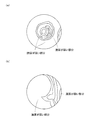
- (A) And (b) is a figure which shows the experimental result which confirms the effect of this invention.
- the magnetron sputtering apparatus SM includes a vacuum chamber 1 that defines a processing chamber 1a.
- An exhaust port 11 is provided at the bottom of the vacuum chamber 1, and the exhaust port 11 is connected to a vacuum pump P such as a turbo molecular pump or a rotary pump via an exhaust pipe 12, and the processing chamber 1 a is set to a predetermined pressure (for example, 1 ⁇ is to be evacuated to 10 -5 Pa).
- a gas inlet 13 is provided on the side wall of the vacuum chamber 1.
- a gas pipe 15 connected to a gas source (not shown) and having a mass flow controller 14 connected to the gas inlet 13 is connected to the gas inlet 13.
- a sputtering gas composed of a rare gas can be introduced into the processing chamber 1a at a predetermined flow rate.
- a substrate stage 16 is disposed on the bottom of the vacuum chamber 1 so as to face a target described later.
- the substrate stage 16 has a known electrostatic chuck (not shown). By applying a predetermined voltage to the electrode of the electrostatic chuck, the substrate W to be processed is placed on the substrate stage 16 with its film formation surface facing up. It can be held by suction.
- a cathode unit C is detachably provided on the ceiling of the vacuum chamber 1.
- the cathode unit C is bonded to a target 2 installed so as to face the inside of the vacuum chamber 1 (processing chamber 1a) and a surface facing the sputtering surface 2a of the target 2 via a bonding material such as indium or tin.
- It has a backing plate 3 and a magnet unit 4 that is disposed on the side opposite to the sputtering surface 2a of the target 2 and generates a leakage magnetic field on the sputtering surface 2a side.
- the backing plate 3 and the magnet unit 4 are surrounded by a housing H.
- the target 2 is made of an insulating material such as alumina (Al 2 O 3 ), which is appropriately selected according to the composition of the thin film to be formed, and is made, for example, circular in plan view using a known method.
- the target 2 is connected to an output from a high-frequency power source as the sputtering power source E, and high-frequency power is input during sputtering.
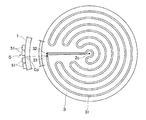
- the backing plate 3 is made of a metal such as Cu having good thermal conductivity, and has a refrigerant circulation passage 31 formed therein, and a refrigerant inlet 32 and an outlet 33 are provided on the upper wall.
- a refrigerant for example, cooling water supplied from a chiller (not shown) is supplied from the inlet 32 to the refrigerant circulation passage 31, and the refrigerant circulated through the refrigerant circulation passage 31 is discharged from the outlet 33 while exchanging heat with the refrigerant.
- the target 2 can be cooled.
- a drive shaft 44a of a drive source 44 is connected to the upper surface of the yoke 41 so that the magnet unit 4 can be driven to rotate about the center of the target 2 while the target 2 is formed by sputtering.
- the magnetron sputtering apparatus SM has known control means including a microcomputer, a sequencer, etc., and controls the operation of the mass flow controller 10, the operation of the vacuum exhaust means P, the drive of the drive source 44, the drive of the chiller, etc. I am doing so.
- control means including a microcomputer, a sequencer, etc., and controls the operation of the mass flow controller 10, the operation of the vacuum exhaust means P, the drive of the drive source 44, the drive of the chiller, etc. I am doing so.
- a sputtering method using the sputtering apparatus SM will be described by taking an example in which an alumina film is formed.
- the vacuum chamber 1 in which the alumina target 2 is disposed is evacuated to a predetermined degree of vacuum (for example, 1 ⁇ 10 ⁇ 5 Pa), and the substrate W is transferred into the vacuum chamber 1 by a transfer robot (not shown).
- the substrate W is transferred to the substrate stage 2 and electrostatically attracted.
- argon gas as a sputtering gas is introduced at a flow rate of, for example, 150 to 250 sccm (at this time, the pressure in the vacuum chamber 1 is 2 to 4 Pa), and high frequency power (for example, 13.56 MHz, 4 kW) to form plasma in the vacuum chamber 1.
- the sputtering surface 2a of the target 2 is sputtered, and the sputtered particles that have scattered are deposited and deposited on the surface of the substrate W to form an alumina film.
- the positions of the first and second magnets 42 and 43 of the magnet unit 4 are designed so that the in-plane distribution of the alumina film formed on the processing substrate W is good. It is known that the thickness distribution of the thin film formed on the processing substrate W is biased due to the position 11 and the position of the gas inlet 13. In the present embodiment, it has been found that the film thickness at the portion of the outlet 33 that discharges the refrigerant from the refrigerant circulation passage 31 of the backing plate 3 is thin, and as a result, the distribution of the film thickness is uneven.
- the vacuum chamber is aligned with the orientation of the bias of the film thickness distribution, that is, across the intersection Cp between the line extending from the center of the target 2 through the outlet 33 and the outer wall of the vacuum chamber 1.
- the auxiliary magnet unit 5 was locally provided on the outer wall of 1.
- the auxiliary magnet unit 5 can be constituted by a plurality (four in this embodiment) of magnets 51 arranged in a circumferential direction.
- these several magnets 51 make a pair, respectively.
- the plasma magnetic field in the vicinity of the outlet is increased by the action of the leakage magnetic field generated in the vacuum chamber 1 by the auxiliary magnet unit 5, and the uneven distribution of the film thickness is effectively suppressed.
- the film thickness in-plane distribution can be improved.
- the following experiment was performed using the magnetron sputtering apparatus SM.
- a silicon substrate having a diameter of 300 mm was used as the processing substrate W, and a target made of aluminum oxide having a diameter of 400 mm was used as the target 2 of the cathode unit C.
- the cathode unit C was assembled, and the four magnets 51 of the auxiliary magnet unit 5 were provided on the outer wall of the vacuum chamber 1 so as to straddle the intersection Cp as shown in FIG.
- the magnet unit 4 is rotated at a rotational speed of 40 rpm, and argon gas is introduced into the vacuum chamber 1 at a flow rate of 200 sccm (processing at this time).
- the pressure inside the chamber 1a was 3 Pa), and 4kW of 13.56 MHz high frequency power was applied to the target 2 to generate plasma, and an alumina film was formed on the processing substrate W by sputtering.
- the average film thickness of the formed alumina film is 45.61 nm, the film thickness in-plane distribution ( ⁇ ) is 0.55%, and as shown in FIG. It was confirmed that the portion having the thickness was substantially concentric and the uneven thickness distribution was suppressed. Note that the direction shown in FIG. 3A corresponds to the direction shown in FIG.
- a comparative experiment was conducted for comparison with the above invention experiment.
- an alumina film was formed using the same conditions as the above-described invention except that the auxiliary magnet unit 5 was not provided.
- the average film thickness of the formed alumina film is 46.16 nm and the film thickness in-plane distribution ( ⁇ ) is 1.19%.
- ⁇ film thickness in-plane distribution
- the film thickness distribution was biased such that the film thickness was thinner and the film thickness increased toward the right side.
- the auxiliary magnet unit 5 by providing the auxiliary magnet unit 5 locally on the outer wall of the vacuum chamber 1, it is possible to suppress the deviation of the film thickness distribution, and consequently the film thickness in-plane distribution is less than 0.6%. It was found that it can be greatly improved.
- the present invention is not limited to the above.
- the case where the auxiliary magnet unit 5 is provided on the outer wall of the vacuum chamber 1 has been described as an example.
- the auxiliary magnet unit 5 may be provided on the outer wall of the housing H so as to match the unevenness of the film thickness distribution.
- the auxiliary magnet unit 5 is comprised with the four magnets 51, what is necessary is just to set the number of the magnets 51 suitably according to the range which acts on a leakage magnetic field.
- the aluminum oxide was demonstrated to the example as a material of the target 2, not only this but insulators, such as MgO, SiC, SiN, can be selected, and metals, such as Ti, Cu, and Al, can be selected. You can choose.
- insulators such as MgO, SiC, SiN
- metals such as Ti, Cu, and Al. You can choose.
- a known DC power source may be used as the sputtering power source E.
- SM magnetron sputtering apparatus
- C cathode unit
- Cp intersection of a line extending from the target center 2c through the outlet 33 and the outer wall of the vacuum chamber 1
- H housing
- W processing substrate
- 2 ... Target 2a ... Sputtering surface
- 2c Center of target 2
- 3 Backing plate
Landscapes
- Chemical & Material Sciences (AREA)
- Engineering & Computer Science (AREA)
- Physics & Mathematics (AREA)
- Plasma & Fusion (AREA)
- Analytical Chemistry (AREA)
- Chemical Kinetics & Catalysis (AREA)
- Materials Engineering (AREA)
- Mechanical Engineering (AREA)
- Metallurgy (AREA)
- Organic Chemistry (AREA)
- Physical Vapour Deposition (AREA)
- Formation Of Insulating Films (AREA)
Abstract
Description
Claims (2)
- 真空チャンバと、この真空チャンバに着脱自在なカソードユニットとを備え、カソードユニットは、真空チャンバ内を臨むように設置されるターゲットと、ターゲットのスパッタ面と背向する側に配置されてスパッタ面側に漏洩磁場を発生させる磁石ユニットとを有するマグネトロンスパッタリング装置であって、真空チャンバ内でターゲットに対向配置される処理基板に対してターゲットをスパッタリングして成膜する間、ターゲット中心を回転中心として磁石ユニットを回転駆動する駆動源を有するものにおいて、
前記処理基板に成膜したときに生じる膜厚分布の偏りの方位に一致させて真空チャンバまたはカソードユニットのハウジングの外壁に、真空チャンバ内に漏洩磁場を作用させる補助磁石ユニットを局所的に設けることを特徴とするマグネトロンスパッタリング装置。 - 請求項1記載のマグネトロンスパッタリング装置であって、
前記ターゲットが絶縁物製であり、このターゲットが、内部に冷媒循環通路が設けられたバッキングプレートに接合された状態でカソードユニットに設けられ、
高周波電力を投入してターゲットをスパッタリングして成膜する間、バッキングプレートの上壁に設けた冷媒の流入口から冷媒循環通路に冷媒を供給し、その上壁に設けた冷媒の流出口から排出しながら冷媒との熱交換でターゲットを冷却するようにしたものにおいて、
前記補助磁石ユニットが、ターゲットの中心から流出口を経てのびる線と真空チャンバの外壁との交点を跨ぐように配置されることを特徴とするマグネトロンスパッタリング装置。
Priority Applications (5)
| Application Number | Priority Date | Filing Date | Title |
|---|---|---|---|
| KR1020177036035A KR20180011151A (ko) | 2015-05-22 | 2016-05-11 | 마그네트론 스퍼터링 장치 |
| JP2017520213A JP6559233B2 (ja) | 2015-05-22 | 2016-05-11 | マグネトロンスパッタリング装置 |
| CN201680029753.2A CN107614748B (zh) | 2015-05-22 | 2016-05-11 | 磁控溅射装置 |
| SG11201709089YA SG11201709089YA (en) | 2015-05-22 | 2016-05-11 | Magnetron sputtering apparatus |
| US15/571,574 US20180155821A1 (en) | 2015-05-22 | 2016-05-11 | Magnetron Sputtering Apparatus |
Applications Claiming Priority (2)
| Application Number | Priority Date | Filing Date | Title |
|---|---|---|---|
| JP2015-104441 | 2015-05-22 | ||
| JP2015104441 | 2015-05-22 |
Publications (1)
| Publication Number | Publication Date |
|---|---|
| WO2016189809A1 true WO2016189809A1 (ja) | 2016-12-01 |
Family
ID=57393969
Family Applications (1)
| Application Number | Title | Priority Date | Filing Date |
|---|---|---|---|
| PCT/JP2016/002308 Ceased WO2016189809A1 (ja) | 2015-05-22 | 2016-05-11 | マグネトロンスパッタリング装置 |
Country Status (7)
| Country | Link |
|---|---|
| US (1) | US20180155821A1 (ja) |
| JP (1) | JP6559233B2 (ja) |
| KR (1) | KR20180011151A (ja) |
| CN (1) | CN107614748B (ja) |
| SG (1) | SG11201709089YA (ja) |
| TW (1) | TWI686492B (ja) |
| WO (1) | WO2016189809A1 (ja) |
Cited By (1)
| Publication number | Priority date | Publication date | Assignee | Title |
|---|---|---|---|---|
| KR20180069014A (ko) * | 2016-05-23 | 2018-06-22 | 가부시키가이샤 알박 | 성막 방법 및 스퍼터링 장치 |
Families Citing this family (6)
| Publication number | Priority date | Publication date | Assignee | Title |
|---|---|---|---|---|
| CN107369602B (zh) * | 2016-05-12 | 2019-02-19 | 北京北方华创微电子装备有限公司 | 反应腔室及半导体加工设备 |
| KR102611646B1 (ko) * | 2018-08-27 | 2023-12-11 | 가부시키가이샤 알박 | 스퍼터링 장치 및 성막 방법 |
| CN109112496B (zh) * | 2018-09-26 | 2020-11-24 | 武汉华星光电半导体显示技术有限公司 | 磁控溅射设备及去除基板上氧化层的方法 |
| WO2020066247A1 (ja) * | 2018-09-27 | 2020-04-02 | 株式会社アルバック | マグネトロンスパッタリング装置用の磁石ユニット |
| JP7057442B2 (ja) * | 2018-11-16 | 2022-04-19 | 株式会社アルバック | 真空処理装置 |
| CN113529030A (zh) * | 2021-08-20 | 2021-10-22 | 浙江最成半导体科技有限公司 | 靶材组件及其制作方法 |
Citations (5)
| Publication number | Priority date | Publication date | Assignee | Title |
|---|---|---|---|---|
| JP2002521567A (ja) * | 1998-07-20 | 2002-07-16 | 東京エレクトロン株式会社 | 不均一性補償を伴う表面の物理的気相処理 |
| JP2005509747A (ja) * | 2001-11-14 | 2005-04-14 | アプライド マテリアルズ インコーポレイテッド | プラズマスパッタリング用回転マグネトロンを組み合わせたマグネットアレイ |
| JP2008214709A (ja) * | 2007-03-06 | 2008-09-18 | Toshiba Corp | マグネトロンスパッタ装置 |
| JP2008255456A (ja) * | 2007-04-09 | 2008-10-23 | Canon Anelva Corp | スパッタリング装置 |
| JP2011117019A (ja) * | 2009-12-01 | 2011-06-16 | Showa Denko Kk | マグネトロンスパッタ装置、インライン式成膜装置、磁気記録媒体の製造方法、磁気記録再生装置 |
Family Cites Families (5)
| Publication number | Priority date | Publication date | Assignee | Title |
|---|---|---|---|---|
| TW271490B (ja) * | 1993-05-05 | 1996-03-01 | Varian Associates | |
| US6039848A (en) * | 1995-07-10 | 2000-03-21 | Cvc Products, Inc. | Ultra-high vacuum apparatus and method for high productivity physical vapor deposition. |
| KR100993046B1 (ko) * | 2001-11-14 | 2010-11-08 | 어플라이드 머티어리얼스, 인코포레이티드 | 스퍼터링 및 재스퍼터링을 위한 자기-이온화 및 유도 결합플라즈마 |
| CN101418433A (zh) * | 2008-10-17 | 2009-04-29 | 湖南玉丰真空科学技术有限公司 | 一种可提高靶材利用率的平面磁控溅射阴极 |
| JP6030404B2 (ja) * | 2012-10-22 | 2016-11-24 | 株式会社アルバック | スパッタリング装置 |
-
2016
- 2016-05-11 SG SG11201709089YA patent/SG11201709089YA/en unknown
- 2016-05-11 CN CN201680029753.2A patent/CN107614748B/zh active Active
- 2016-05-11 US US15/571,574 patent/US20180155821A1/en not_active Abandoned
- 2016-05-11 WO PCT/JP2016/002308 patent/WO2016189809A1/ja not_active Ceased
- 2016-05-11 KR KR1020177036035A patent/KR20180011151A/ko not_active Ceased
- 2016-05-11 JP JP2017520213A patent/JP6559233B2/ja active Active
- 2016-05-19 TW TW105115557A patent/TWI686492B/zh active
Patent Citations (5)
| Publication number | Priority date | Publication date | Assignee | Title |
|---|---|---|---|---|
| JP2002521567A (ja) * | 1998-07-20 | 2002-07-16 | 東京エレクトロン株式会社 | 不均一性補償を伴う表面の物理的気相処理 |
| JP2005509747A (ja) * | 2001-11-14 | 2005-04-14 | アプライド マテリアルズ インコーポレイテッド | プラズマスパッタリング用回転マグネトロンを組み合わせたマグネットアレイ |
| JP2008214709A (ja) * | 2007-03-06 | 2008-09-18 | Toshiba Corp | マグネトロンスパッタ装置 |
| JP2008255456A (ja) * | 2007-04-09 | 2008-10-23 | Canon Anelva Corp | スパッタリング装置 |
| JP2011117019A (ja) * | 2009-12-01 | 2011-06-16 | Showa Denko Kk | マグネトロンスパッタ装置、インライン式成膜装置、磁気記録媒体の製造方法、磁気記録再生装置 |
Cited By (2)
| Publication number | Priority date | Publication date | Assignee | Title |
|---|---|---|---|---|
| KR20180069014A (ko) * | 2016-05-23 | 2018-06-22 | 가부시키가이샤 알박 | 성막 방법 및 스퍼터링 장치 |
| KR102138598B1 (ko) | 2016-05-23 | 2020-07-28 | 가부시키가이샤 알박 | 성막 방법 및 스퍼터링 장치 |
Also Published As
| Publication number | Publication date |
|---|---|
| US20180155821A1 (en) | 2018-06-07 |
| JP6559233B2 (ja) | 2019-08-14 |
| TWI686492B (zh) | 2020-03-01 |
| TW201708583A (zh) | 2017-03-01 |
| SG11201709089YA (en) | 2017-12-28 |
| JPWO2016189809A1 (ja) | 2018-03-01 |
| KR20180011151A (ko) | 2018-01-31 |
| CN107614748A (zh) | 2018-01-19 |
| CN107614748B (zh) | 2019-09-10 |
Similar Documents
| Publication | Publication Date | Title |
|---|---|---|
| JP6559233B2 (ja) | マグネトロンスパッタリング装置 | |
| TWI780173B (zh) | 濺鍍裝置 | |
| JP6171108B2 (ja) | 成膜装置及び成膜方法 | |
| TW201831718A (zh) | 具有背側冷卻溝槽的濺射靶材 | |
| JP6471000B2 (ja) | マグネトロンスパッタリング装置用の磁石ユニット及びこの磁石ユニットを用いたスパッタリング方法 | |
| JP6641472B2 (ja) | 成膜方法及びスパッタリング装置 | |
| JP7326036B2 (ja) | マグネトロンスパッタリング装置用のカソードユニット | |
| TWI770421B (zh) | 濺鍍裝置及濺鍍方法 | |
| JP6030813B1 (ja) | 高周波スパッタリング装置及びスパッタリング方法 | |
| JP6636796B2 (ja) | スパッタリング装置及びスパッタリング方法 | |
| JP6088780B2 (ja) | プラズマ処理方法及びプラズマ処理装置 | |
| JP2019019376A (ja) | 成膜方法及びスパッタリング装置 | |
| JP6641382B2 (ja) | カーボン膜の成膜方法 | |
| JP6335386B2 (ja) | カソードアッセンブリ | |
| JP2016117923A (ja) | スパッタリング装置 | |
| WO2017221650A1 (ja) | 成膜方法 | |
| JP2014181376A (ja) | スパッタリング装置及びスパッタリング方法 | |
| JP2016216764A (ja) | マグネトロンスパッタリング装置用のカソードユニット及びこのカソードユニットを用いたスパッタリング方法 |
Legal Events
| Date | Code | Title | Description |
|---|---|---|---|
| 121 | Ep: the epo has been informed by wipo that ep was designated in this application |
Ref document number: 16799524 Country of ref document: EP Kind code of ref document: A1 |
|
| WWE | Wipo information: entry into national phase |
Ref document number: 11201709089Y Country of ref document: SG Ref document number: 15571574 Country of ref document: US |
|
| ENP | Entry into the national phase |
Ref document number: 2017520213 Country of ref document: JP Kind code of ref document: A |
|
| NENP | Non-entry into the national phase |
Ref country code: DE |
|
| ENP | Entry into the national phase |
Ref document number: 20177036035 Country of ref document: KR Kind code of ref document: A |
|
| 122 | Ep: pct application non-entry in european phase |
Ref document number: 16799524 Country of ref document: EP Kind code of ref document: A1 |