WO2016185941A1 - マスクブランク、転写用マスク、転写用マスクの製造方法および半導体デバイスの製造方法 - Google Patents
マスクブランク、転写用マスク、転写用マスクの製造方法および半導体デバイスの製造方法 Download PDFInfo
- Publication number
- WO2016185941A1 WO2016185941A1 PCT/JP2016/063843 JP2016063843W WO2016185941A1 WO 2016185941 A1 WO2016185941 A1 WO 2016185941A1 JP 2016063843 W JP2016063843 W JP 2016063843W WO 2016185941 A1 WO2016185941 A1 WO 2016185941A1
- Authority
- WO
- WIPO (PCT)
- Prior art keywords
- film
- phase shift
- pattern
- mask
- etching
- Prior art date
- Legal status (The legal status is an assumption and is not a legal conclusion. Google has not performed a legal analysis and makes no representation as to the accuracy of the status listed.)
- Ceased
Links
Images



Classifications
-
- G—PHYSICS
- G03—PHOTOGRAPHY; CINEMATOGRAPHY; ANALOGOUS TECHNIQUES USING WAVES OTHER THAN OPTICAL WAVES; ELECTROGRAPHY; HOLOGRAPHY
- G03F—PHOTOMECHANICAL PRODUCTION OF TEXTURED OR PATTERNED SURFACES, e.g. FOR PRINTING, FOR PROCESSING OF SEMICONDUCTOR DEVICES; MATERIALS THEREFOR; ORIGINALS THEREFOR; APPARATUS SPECIALLY ADAPTED THEREFOR
- G03F1/00—Originals for photomechanical production of textured or patterned surfaces, e.g., masks, photo-masks, reticles; Mask blanks or pellicles therefor; Containers specially adapted therefor; Preparation thereof
- G03F1/26—Phase shift masks [PSM]; PSM blanks; Preparation thereof
-
- G—PHYSICS
- G03—PHOTOGRAPHY; CINEMATOGRAPHY; ANALOGOUS TECHNIQUES USING WAVES OTHER THAN OPTICAL WAVES; ELECTROGRAPHY; HOLOGRAPHY
- G03F—PHOTOMECHANICAL PRODUCTION OF TEXTURED OR PATTERNED SURFACES, e.g. FOR PRINTING, FOR PROCESSING OF SEMICONDUCTOR DEVICES; MATERIALS THEREFOR; ORIGINALS THEREFOR; APPARATUS SPECIALLY ADAPTED THEREFOR
- G03F1/00—Originals for photomechanical production of textured or patterned surfaces, e.g., masks, photo-masks, reticles; Mask blanks or pellicles therefor; Containers specially adapted therefor; Preparation thereof
- G03F1/26—Phase shift masks [PSM]; PSM blanks; Preparation thereof
- G03F1/32—Attenuating PSM [att-PSM], e.g. halftone PSM or PSM having semi-transparent phase shift portion; Preparation thereof
-
- G—PHYSICS
- G03—PHOTOGRAPHY; CINEMATOGRAPHY; ANALOGOUS TECHNIQUES USING WAVES OTHER THAN OPTICAL WAVES; ELECTROGRAPHY; HOLOGRAPHY
- G03F—PHOTOMECHANICAL PRODUCTION OF TEXTURED OR PATTERNED SURFACES, e.g. FOR PRINTING, FOR PROCESSING OF SEMICONDUCTOR DEVICES; MATERIALS THEREFOR; ORIGINALS THEREFOR; APPARATUS SPECIALLY ADAPTED THEREFOR
- G03F1/00—Originals for photomechanical production of textured or patterned surfaces, e.g., masks, photo-masks, reticles; Mask blanks or pellicles therefor; Containers specially adapted therefor; Preparation thereof
- G03F1/38—Masks having auxiliary features, e.g. special coatings or marks for alignment or testing; Preparation thereof
- G03F1/48—Protective coatings
-
- G—PHYSICS
- G03—PHOTOGRAPHY; CINEMATOGRAPHY; ANALOGOUS TECHNIQUES USING WAVES OTHER THAN OPTICAL WAVES; ELECTROGRAPHY; HOLOGRAPHY
- G03F—PHOTOMECHANICAL PRODUCTION OF TEXTURED OR PATTERNED SURFACES, e.g. FOR PRINTING, FOR PROCESSING OF SEMICONDUCTOR DEVICES; MATERIALS THEREFOR; ORIGINALS THEREFOR; APPARATUS SPECIALLY ADAPTED THEREFOR
- G03F1/00—Originals for photomechanical production of textured or patterned surfaces, e.g., masks, photo-masks, reticles; Mask blanks or pellicles therefor; Containers specially adapted therefor; Preparation thereof
- G03F1/50—Mask blanks not covered by G03F1/20 - G03F1/34; Preparation thereof
-
- G—PHYSICS
- G03—PHOTOGRAPHY; CINEMATOGRAPHY; ANALOGOUS TECHNIQUES USING WAVES OTHER THAN OPTICAL WAVES; ELECTROGRAPHY; HOLOGRAPHY
- G03F—PHOTOMECHANICAL PRODUCTION OF TEXTURED OR PATTERNED SURFACES, e.g. FOR PRINTING, FOR PROCESSING OF SEMICONDUCTOR DEVICES; MATERIALS THEREFOR; ORIGINALS THEREFOR; APPARATUS SPECIALLY ADAPTED THEREFOR
- G03F1/00—Originals for photomechanical production of textured or patterned surfaces, e.g., masks, photo-masks, reticles; Mask blanks or pellicles therefor; Containers specially adapted therefor; Preparation thereof
- G03F1/54—Absorbers, e.g. of opaque materials
-
- G—PHYSICS
- G03—PHOTOGRAPHY; CINEMATOGRAPHY; ANALOGOUS TECHNIQUES USING WAVES OTHER THAN OPTICAL WAVES; ELECTROGRAPHY; HOLOGRAPHY
- G03F—PHOTOMECHANICAL PRODUCTION OF TEXTURED OR PATTERNED SURFACES, e.g. FOR PRINTING, FOR PROCESSING OF SEMICONDUCTOR DEVICES; MATERIALS THEREFOR; ORIGINALS THEREFOR; APPARATUS SPECIALLY ADAPTED THEREFOR
- G03F1/00—Originals for photomechanical production of textured or patterned surfaces, e.g., masks, photo-masks, reticles; Mask blanks or pellicles therefor; Containers specially adapted therefor; Preparation thereof
- G03F1/68—Preparation processes not covered by groups G03F1/20 - G03F1/50
- G03F1/72—Repair or correction of mask defects
- G03F1/74—Repair or correction of mask defects by charged particle beam [CPB], e.g. focused ion beam
-
- G—PHYSICS
- G03—PHOTOGRAPHY; CINEMATOGRAPHY; ANALOGOUS TECHNIQUES USING WAVES OTHER THAN OPTICAL WAVES; ELECTROGRAPHY; HOLOGRAPHY
- G03F—PHOTOMECHANICAL PRODUCTION OF TEXTURED OR PATTERNED SURFACES, e.g. FOR PRINTING, FOR PROCESSING OF SEMICONDUCTOR DEVICES; MATERIALS THEREFOR; ORIGINALS THEREFOR; APPARATUS SPECIALLY ADAPTED THEREFOR
- G03F1/00—Originals for photomechanical production of textured or patterned surfaces, e.g., masks, photo-masks, reticles; Mask blanks or pellicles therefor; Containers specially adapted therefor; Preparation thereof
- G03F1/68—Preparation processes not covered by groups G03F1/20 - G03F1/50
- G03F1/76—Patterning of masks by imaging
- G03F1/78—Patterning of masks by imaging by charged particle beam [CPB], e.g. electron beam patterning of masks
-
- G—PHYSICS
- G03—PHOTOGRAPHY; CINEMATOGRAPHY; ANALOGOUS TECHNIQUES USING WAVES OTHER THAN OPTICAL WAVES; ELECTROGRAPHY; HOLOGRAPHY
- G03F—PHOTOMECHANICAL PRODUCTION OF TEXTURED OR PATTERNED SURFACES, e.g. FOR PRINTING, FOR PROCESSING OF SEMICONDUCTOR DEVICES; MATERIALS THEREFOR; ORIGINALS THEREFOR; APPARATUS SPECIALLY ADAPTED THEREFOR
- G03F1/00—Originals for photomechanical production of textured or patterned surfaces, e.g., masks, photo-masks, reticles; Mask blanks or pellicles therefor; Containers specially adapted therefor; Preparation thereof
- G03F1/68—Preparation processes not covered by groups G03F1/20 - G03F1/50
- G03F1/80—Etching
-
- H—ELECTRICITY
- H10—SEMICONDUCTOR DEVICES; ELECTRIC SOLID-STATE DEVICES NOT OTHERWISE PROVIDED FOR
- H10P—GENERIC PROCESSES OR APPARATUS FOR THE MANUFACTURE OR TREATMENT OF DEVICES COVERED BY CLASS H10
- H10P50/00—Etching of wafers, substrates or parts of devices
- H10P50/20—Dry etching; Plasma etching; Reactive-ion etching
- H10P50/24—Dry etching; Plasma etching; Reactive-ion etching of semiconductor materials
- H10P50/242—Dry etching; Plasma etching; Reactive-ion etching of semiconductor materials of Group IV materials
-
- H—ELECTRICITY
- H10—SEMICONDUCTOR DEVICES; ELECTRIC SOLID-STATE DEVICES NOT OTHERWISE PROVIDED FOR
- H10P—GENERIC PROCESSES OR APPARATUS FOR THE MANUFACTURE OR TREATMENT OF DEVICES COVERED BY CLASS H10
- H10P76/00—Manufacture or treatment of masks on semiconductor bodies, e.g. by lithography or photolithography
- H10P76/40—Manufacture or treatment of masks on semiconductor bodies, e.g. by lithography or photolithography of masks comprising inorganic materials
- H10P76/408—Manufacture or treatment of masks on semiconductor bodies, e.g. by lithography or photolithography of masks comprising inorganic materials characterised by their sizes, orientations, dispositions, behaviours or shapes
- H10P76/4085—Manufacture or treatment of masks on semiconductor bodies, e.g. by lithography or photolithography of masks comprising inorganic materials characterised by their sizes, orientations, dispositions, behaviours or shapes characterised by the processes involved to create the masks
Definitions
- the present invention relates to a mask blank, a transfer mask manufactured using the mask blank, and a manufacturing method thereof.
- the present invention also relates to a method for manufacturing a semiconductor device using the transfer mask.
- a fine pattern is formed using a photolithography method.
- a number of transfer masks are usually used for forming this fine pattern.
- miniaturizing a semiconductor device pattern it is necessary to shorten the wavelength of an exposure light source used in photolithography in addition to miniaturization of a mask pattern formed on a transfer mask.
- the exposure light source used in the manufacture of semiconductor devices has been shortened from a KrF excimer laser (wavelength 248 nm) to an ArF excimer laser (wavelength 193 nm).
- phase shift mask As a type of transfer mask, there is a halftone phase shift mask in addition to a binary mask having a light-shielding film pattern made of a chromium-based material on a conventional translucent substrate.
- a molybdenum silicide (MoSi) -based material is widely used as disclosed in Patent Document 1.
- Patent Document 2 there is also known a phase shift mask including a phase shift film having a relatively high transmittance of 9% or more for exposure light although it is a molybdenum silicide material. .
- Patent Document 3 discloses a defect in which a black defect portion of a light-shielding film is etched and removed by irradiating an electron beam to the portion while supplying xenon difluoride (XeF 2 ) gas.
- a correction technique hereinafter, such defect correction performed by irradiating charged particles such as an electron beam is simply referred to as EB defect correction
- This EB defect correction was originally used for black defect correction in the absorber film of the reflective mask for EUV lithography (Extreme Ultraviolet Lithography), but in recent years it has also been used in black defect correction for MoSi halftone masks. Yes.
- a phase shift film made of a molybdenum silicide material and a silicon material generally forms a phase shift pattern by dry etching using a fluorine-based gas as an etching gas.
- the phase shift film of these materials does not have very high etching selectivity of dry etching with a fluorine-based gas with respect to a substrate made of a glass material.
- the etching stopper film made of Al 2 O 3 is excellent in resistance to dry etching by a fluorine-based gas, and has an advantage that it is possible to prevent the substrate from being dug during dry etching of the phase shift film. is there. Further, the etching stopper film made of Al 2 O 3 has high resistance to EB defect correction, and it is also possible to suppress damage to the substrate that is likely to occur when EB defect correction is performed on the black defect portion of the phase shift film. is there. However, an etching stopper film made of Al 2 O 3 tends to have low resistance to chemical cleaning. During the process of manufacturing a phase shift mask (transfer mask) from a mask blank, cleaning with a chemical solution is performed many times.
- the completed phase shift mask is periodically cleaned with a chemical solution.
- TMAH tetramethylammonium hydroxide
- TMAH tetramethylammonium hydroxide
- phase shift mask including a phase shift film in which an etching stopper film made of Al 2 O 3 and a phase shift pattern are formed on a light-transmitting substrate made of glass is washed with ammonia overwater
- the etching stopper film immediately below the pattern portion where the phase shift film exists also dissolves from the side wall side to the inside side of the phase shift film.
- the width of the etching stopper film remaining without being dissolved is larger than the pattern width of the phase shift film. It gets smaller. In such a state, a phenomenon in which the pattern of the phase shift film is dropped easily occurs.
- the exposure light is provided with a phase shift pattern of a light-transmitting substrate of the phase shift mask.
- the light enters from the main surface opposite to the main surface, and enters the phase shift pattern via the etching stopper film.
- the pattern formed on the phase shift film of the phase shift mask is designed on the assumption that an etching stopper film exists between the translucent substrate and the phase shift film. For this reason, in the state where the etching stopper film of the phase shift mask is dissolved, there is a possibility that the optical characteristics expected at the time of designing the phase shift pattern cannot be sufficiently obtained.
- the etching stopper film made of Al 2 O 3 has a problem that the transmittance with respect to the exposure light is lower than that of the synthetic quartz glass used as the material of the light-transmitting substrate of the phase shift mask. In the case of a phase shift mask in which an ArF excimer laser is applied to exposure light, this tendency appears more remarkably.
- the etching stopper film made of Al 2 O 3 is also left in the translucent part when the phase shift mask is completed. A decrease in the transmittance of the exposure light in the light transmitting portion of the phase shift mask leads to a decrease in the phase shift effect in the phase shift mask.
- a transition metal silicide material is used as a material for a light shielding film in a mask blank for manufacturing a binary transfer mask having a light shielding film pattern having a high optical density on a translucent substrate. . Even when a pattern is formed on the light shielding film of the transition metal silicide material, dry etching using fluorine gas is used.
- the light shielding film transition metal silicide-based material may be required to have a high optical density, and the degree of nitridation or oxidation tends not to be higher than that of the phase shift film transition metal silicide-based material.
- the etching selectivity with respect to the dry etching by the fluorine-type gas between a light shielding film and a translucent substrate tends to become larger than the selectivity between a phase shift film and a translucent substrate.
- such etching selectivity may not be sufficient to suppress the etching of the light-transmitting substrate, and it is desired to provide an etching stopper film between the light-transmitting substrate and the light shielding film.
- a transfer mask is manufactured from a mask blank having a light shielding film made of this transition metal silicide material, EB defect correction is performed even when a black defect portion is found in the pattern of the light shielding film. It is effective to provide an etching stopper film in order to suppress damage to the substrate during EB defect correction. Also, in the case of the etching stopper film in this binary type transfer mask, it is necessary to be a material having high resistance to chemical cleaning, as in the case of the phase shift mask, and it is a material having a high transmittance for exposure light. It is also desired.
- the present invention has been made to solve the above-described conventional problems, and is a mask blank having a pattern forming thin film such as a phase shift film or a light shielding film on a light transmissive substrate.
- a pattern forming thin film such as a phase shift film or a light shielding film on a light transmissive substrate.
- an etching stopper film is interposed between the forming thin films, the resistance to dry etching by the fluorine-based gas used when patterning the pattern forming thin film is high, the resistance to chemical cleaning is high, and the exposure light
- It aims at providing the mask blank provided with the etching stopper film
- An object of the present invention is to provide a method of manufacturing a semiconductor device using such a transfer mask.
- the present invention has the following configuration.
- (Configuration 1) A mask blank provided with a thin film for pattern formation on the main surface of a translucent substrate, The pattern forming thin film contains silicon, An etching stopper film between the translucent substrate and the pattern forming thin film; A mask blank, wherein the etching stopper film contains silicon, aluminum, and oxygen.
- (Configuration 4) 4. The mask blank according to any one of configurations 1 to 3, wherein the etching stopper film is made of silicon, aluminum, and oxygen.
- the phase shift film has a function of transmitting exposure light with a transmittance of 1% or more, and the exposure light transmitted through the phase shift film passes through the air by the same distance as the thickness of the phase shift film.
- the mask blank according to Configuration 9 which has a function of generating a phase difference of 150 degrees or more and 180 degrees or less with exposure light.
- (Configuration 15) A method for manufacturing a transfer mask using the mask blank according to Configuration 11, comprising: Forming a transfer pattern on the light shielding film by dry etching; Forming a transfer pattern on the phase shift film by dry etching using a fluorine-based gas using the light-shielding film having the transfer pattern as a mask; And a step of forming a pattern including a light-shielding band on the light-shielding film by dry etching.
- the mask blank of the present invention is a mask blank provided with a thin film for pattern formation on the main surface of a translucent substrate, the thin film for pattern formation contains silicon, and is composed of a translucent substrate and a thin film for pattern formation. It has an etching stopper film in between, and the etching stopper film is characterized by containing silicon, aluminum and oxygen.
- the etching stopper film has higher resistance to dry etching by a fluorine-based gas performed when forming a pattern on the pattern forming thin film than a translucent substrate. It is possible to simultaneously satisfy the three characteristics of high resistance to light and high transmittance for exposure light.
- Al 2 O 3 which is a material of the etching stopper film has high resistance to dry etching by a fluorine-based gas, but the transmittance for exposure light of an ArF excimer laser (wavelength: about 193 nm) is not so high. Resistance to cleaning liquid used for cleaning is also low.
- SiO 2 which is the main material of the translucent substrate is a material having a high transmittance with respect to exposure light of an ArF excimer laser (wavelength: about 193 nm) and a high resistance to a cleaning liquid used for cleaning a transfer mask. It is also a material that is easily etched against dry etching with a fluorine-based gas. As a result of intensive studies, the inventors of the present invention have formed an etching stopper film made of a material in which Al 2 O 3 and SiO 2 are mixed, thereby being resistant to dry etching by a fluorine-based gas, ArF excimer laser (wavelength: about 193 nm). The possibility of satisfying all of the three conditions of the high transmittance with respect to the exposure light of) and the resistance to the cleaning liquid used for cleaning the transfer mask was found.
- the resistance to dry etching by a fluorine-based gas is inferior to an etching stopper film made of only Al 2 O 3. Is sufficiently high to function sufficiently as an etching stopper film.
- the transmittance of the ArF excimer laser with respect to the exposure light was inferior to that of the material made of only SiO 2, but was found to be much higher than the etching stopper film made of only Al 2 O 3 .
- the resistance to the cleaning liquid (ammonia overwater, TMAH, etc.) was inferior to that of the material made of only SiO 2, but the resistance was much higher than the etching stopper film made of only Al 2 O 3 .
- XeF 2 xenon difluoride
- a process of irradiating the portion with an electron beam is applied to the etching stopper film with a material in which Al 2 O 3 and SiO 2 are mixed.
- the film was inferior to the etching stopper film made only of Al 2 O 3 but sufficiently resistant compared to the material made only of SiO 2 .
- the mask blank of the present invention is a mask blank provided with a thin film for pattern formation on the main surface of a translucent substrate, the thin film for pattern formation contains silicon, and is used for pattern formation with the translucent substrate.
- An etching stopper film is provided between the thin films, and the etching stopper film contains silicon, aluminum, and oxygen.
- the pattern forming thin film is a phase shift film that is a film that imparts a predetermined transmittance and phase difference to exposure light. Transfer mask).
- FIG. 1 shows the configuration of the mask blank of the first embodiment.
- the mask blank 100 according to the first embodiment includes an etching stopper film 2, a phase shift film (pattern forming thin film) 3, a light shielding film 4, and a hard mask film 5 on the main surface of the translucent substrate 1. ing.
- the translucent substrate 1 is not particularly limited as long as it has a high transmittance for exposure light.
- a synthetic quartz glass substrate and other various glass substrates for example, soda lime glass, aluminosilicate glass, etc.
- a synthetic quartz glass substrate is particularly suitable as a mask blank substrate of the present invention used for forming a high-definition transfer pattern because it has a high transmittance in an ArF excimer laser or a shorter wavelength region.
- any of these glass substrates is a material that is easily etched by dry etching using a fluorine-based gas. For this reason, the significance of providing the etching stopper film 2 on the translucent substrate 1 is great.
- Etching stopper film 2 is formed of a material containing silicon, aluminum and oxygen.
- the etching stopper film 2 is left without being removed at least on the entire surface of the transfer pattern forming region when the phase shift mask 200 is completed (see FIG. 2). In other words, the etching stopper film 2 remains in the light-transmitting portion where the phase shift film 3 has no phase shift pattern. For this reason, it is preferable that the etching stopper film 2 is formed in contact with the translucent substrate 1 without interposing another film between the etching stopper film 2 and the translucent substrate 1.
- the etching stopper film 2 is preferably as high as possible with respect to the exposure light. However, since the etching stopper film 2 is required to have sufficient etching selectivity with respect to the fluorine-based gas with the light-transmitting substrate 1, the etching stopper film 2 with respect to the exposure light. It is difficult to make the transmittance the same as that of the translucent substrate 1 (that is, the transmissivity of the etching stopper film 2 when the transmissivity of the translucent substrate 1 (synthetic quartz glass) with respect to exposure light is 100%. Is less than 100%.) The transmittance of the etching stopper film 2 is preferably 95% or more, more preferably 96% or more, and 97% or more when the transmittance of the translucent substrate 1 with respect to exposure light is 100%. And more preferred.
- Etching stopper film 2 preferably has an oxygen content of 60 atomic% or more. This is because the etching stopper film 2 is required to contain a large amount of oxygen in order to set the transmittance for exposure light to the above numerical value or more.
- silicon bonded to oxygen tends to be more resistant to chemical cleaning (especially alkaline cleaning such as ammonia perwater or TMAH) than oxygen unbonded silicon. It is preferable to increase the proportion of all silicon present in the silicon in a bonded state with oxygen.
- the etching stopper film 2 preferably has an oxygen content of 66 atomic% or less.
- the etching stopper film 2 is a ratio of the content (atomic%) of silicon (Si) to the total content (atomic%) of silicon (Si) and aluminum (Al) (hereinafter referred to as “Si / [Si + Al] ratio”). ) Is preferably 4/5 or less.
- Si / [Si + Al] ratio of the etching stopper film 2 is set to 4/5 or less.
- the etching rate of the etching stopper film 2 with respect to the dry etching with the fluorine-based gas is set to 1/3 or less of the etching rate of the translucent substrate 1. (An etching selectivity of 3 times or more can be obtained between the translucent substrate 1 and the etching stopper film 2).
- the Si / [Si + Al] ratio in the etching stopper film 2 is more preferably 3/4 or less, and further preferably 2/3 or less.
- the etching rate of the etching stopper film 2 with respect to dry etching with a fluorine-based gas can be set to 1/5 or less of the etching rate of the translucent substrate 1 (translucent light An etching selectivity of 5 times or more is obtained between the conductive substrate 1 and the etching stopper film 2).
- the etching stopper film 2 preferably has a Si / [Si + Al] ratio of silicon (Si) and aluminum (Al) of 1/5 or more.
- Si silicon
- Al aluminum
- the Si / [Si + Al] ratio of the etching stopper film 2 is set to 1/5 or more, the transmittance of the etching stopper film 2 when the transmittance of the translucent substrate 1 (synthetic quartz glass) with respect to the exposure light is 100%.
- the rate can be 95% or more.
- resistance to chemical cleaning can be increased.
- the Si / [Si + Al] ratio in the etching stopper film 2 is more preferably 1/3 or more.
- the transmittance of the etching stopper film 2 is 97% or more when the transmittance of the translucent substrate (synthetic quartz glass) 1 with respect to exposure light is 100%. be able to.
- the etching stopper film 2 preferably has a content of metal other than aluminum of 2 atomic% or less, more preferably 1 atomic% or less, and is below the lower limit of detection when composition analysis is performed by X-ray photoelectron spectroscopy. More preferably. This is because if the etching stopper film 2 contains a metal other than aluminum, the transmittance with respect to the exposure light decreases.
- the etching stopper film 2 preferably has a total content of elements other than silicon, aluminum and oxygen of 5 atomic% or less, more preferably 3 atomic% or less.
- Etching stopper film 2 may be formed of a material composed of silicon, aluminum, and oxygen.
- the material composed of silicon, aluminum, and oxygen is an element inevitably contained in the etching stopper film 2 (helium (He), neon (Ne), A material containing only a rare gas such as argon (Ar), krypton (Kr), and xenon (Xe), hydrogen (H), carbon (C), or the like).
- the etching stopper film 2 preferably has an amorphous structure. More specifically, it is preferable that the etching stopper film 2 has an amorphous structure including a bond of silicon and oxygen and a bond of aluminum and oxygen. While the surface roughness of the etching stopper film 2 can be improved, the transmittance for exposure light can be increased.
- the etching stopper film 2 preferably has a thickness of 3 nm or more.
- the thickness of the etching stopper film 2 is desirably 3 nm or more.
- the thickness of the etching stopper film 2 is preferably 4 nm or more, and more preferably 5 nm or more.
- the etching stopper film 2 is made of a material having a high transmittance with respect to exposure light, but the transmittance decreases as the thickness increases.
- the etching stopper film 2 has a higher refractive index than the material forming the translucent substrate 1, and the mask pattern (Bias correction or bias pattern) actually formed on the phase shift film 3 increases as the thickness of the etching stopper film 2 increases.
- the influence exerted when designing a pattern is increased.
- the etching stopper film 2 is desired to be 20 nm or less, preferably 15 nm or less, and more preferably 10 nm or less.
- the etching stopper film 2 preferably has a refractive index n (hereinafter simply referred to as refractive index n) of ArF excimer laser exposure light of 1.73 or less, and more preferably 1.72 or less. This is to reduce the influence of designing a mask pattern actually formed on the phase shift film 3. Since the etching stopper film 2 is formed of a material containing aluminum, it cannot have the same refractive index n as that of the translucent substrate 1. The etching stopper film 2 is formed with a refractive index n of 1.57 or more.
- the etching stopper film 2 preferably has an extinction coefficient k (hereinafter, simply referred to as an extinction coefficient k) of 0.04 or less with respect to exposure light of an ArF excimer laser. This is because the transmittance of the etching stopper film 2 to the exposure light is increased.
- the etching stopper film 2 is formed of a material having an extinction coefficient k of 0.000 or more.
- the etching stopper film 2 has high composition uniformity in the thickness direction (the difference in the content of each constituent element in the thickness direction is within a fluctuation range within 5 atomic%).
- the etching stopper film 2 may have a film structure having a composition gradient in the thickness direction.
- the Si / [Si + Al] ratio of the etching stopper film 2 on the translucent substrate 1 side be a composition gradient so as to be higher than the Si / [Si + Al] ratio on the phase shift film 3 side.
- the etching stopper film 2 is preferentially desired that the phase shift film 3 side is highly resistant to dry etching with a fluorine-based gas and has high chemical resistance, whereas the light-transmitting substrate 1 side is more transparent to exposure light. This is because a high rate is desired.
- Another film may be interposed between the translucent substrate 1 and the etching stopper film 2.
- the other films are required to be made of a material having a higher transmittance for exposure light and a smaller refractive index n than the etching stopper film 2.
- the material of the other film examples include a material made of silicon and oxygen, or a material containing one or more elements selected from hafnium, zirconium, titanium, vanadium and boron.
- the other film may be formed of a material containing silicon, aluminum, and oxygen and having a higher Si / [Si + Al] ratio than the etching stopper film 2. Also in this case, the other film has higher transmittance for exposure light, and the refractive index n becomes smaller (closer to the material of the translucent substrate 1).
- the phase shift film 3 is made of a material containing silicon, transmits light having a strength that does not substantially contribute to exposure, and has a predetermined phase difference. Specifically, the phase shift film 3 is patterned to form a portion where the phase shift film 3 remains and a portion where the phase shift film 3 does not remain, and light transmitted through the portion without the phase shift film 3 (ArF excimer laser exposure light). In contrast, the phase of the light transmitted through the phase shift film 3 (light with a strength that does not substantially contribute to exposure) is substantially reversed (predetermined phase difference). By doing so, the light that has entered the other region due to the diffraction phenomenon cancels each other out, and the light intensity at the boundary is made almost zero, thereby improving the contrast of the boundary, that is, the resolution.
- the phase shift film 3 has a function of transmitting exposure light with a transmittance of 1% or more (transmittance), and the exposure light transmitted through the phase shift film is in the air by the same distance as the thickness of the phase shift film. It is preferable to have a function of causing a phase difference of 150 degrees or more and 180 degrees or less with the exposure light that has passed.
- the transmittance of the phase shift film 3 is more preferably 2% or more.
- the transmittance of the phase shift film 3 is preferably 30% or less, and more preferably 20% or less.
- the pattern line width of the phase shift pattern (particularly, line and There is a problem that the difference in the best focus of exposure transfer due to the pattern pitch of the space pattern is large.
- the predetermined phase difference in the phase shift film 3 is preferably set to 170 degrees or less.
- the thickness of the phase shift film 3 is preferably 80 nm or less, and more preferably 70 nm or less. In order to reduce the variation range of the best focus due to the pattern line width of the phase shift pattern, the thickness of the phase shift film 3 is particularly preferably set to 65 nm or less. The thickness of the phase shift film 3 is preferably 50 nm or more. This is because 50 nm or more is necessary to make the phase shift of the phase shift film 3 150 nm or more while forming the phase shift film 3 with an amorphous material.
- the refractive index n with respect to the exposure light (ArF exposure light) of the phase shift film is preferably 1.9 or more in order to satisfy the various conditions concerning the optical characteristics and the film thickness. 0.0 or more is more preferable.
- the refractive index n of the phase shift film 3 is preferably 3.1 or less, and more preferably 2.7 or less.
- the extinction coefficient k for the ArF exposure light of the phase shift film 3 is preferably 0.26 or more, and more preferably 0.29 or more.
- the extinction coefficient k of the phase shift film 3 is preferably 0.62 or less, and more preferably 0.54 or less.
- the phase shift film 3 includes a pair of a low transmission layer formed of a material having a relatively low transmittance to exposure light and a high transmission layer formed of a material having a relatively high transmittance to exposure light.
- a laminated structure is used.
- the low transmission layer has a refractive index n with respect to ArF exposure light of less than 2.5 (preferably 2.4 or less, more preferably 2.2 or less, more preferably 2.0 or less), and extinction. It is preferably formed of a material having a coefficient k of 1.0 or more (preferably 1.1 or more, more preferably 1.4 or more, and further preferably 1.6 or more).
- the high transmission layer has a refractive index n with respect to ArF exposure light of 2.5 or more (preferably 2.6 or more) and an extinction coefficient k of less than 1.0 (preferably 0.9 or less, more preferably 0.7 or less, more preferably 0.4 or less).
- the refractive index n and extinction coefficient k of the thin film including the phase shift film 3 are not determined only by the composition of the thin film.
- the film density and crystal state of the thin film are factors that influence the refractive index n and the extinction coefficient k. For this reason, various conditions when forming a thin film by reactive sputtering are adjusted so that the thin film has a desired refractive index n and extinction coefficient k.
- a mixed gas of a rare gas and a reactive gas oxygen gas, nitrogen gas, etc.
- the phase shift film 3 made of a material containing silicon is patterned by dry etching using a fluorine-based gas.
- the translucent substrate 1 made of a glass material is easily etched by dry etching with a fluorine-based gas, and particularly has low resistance to a fluorine-based gas containing carbon. For this reason, when patterning the phase shift film 3, dry etching using a fluorine-based gas (SF 6 or the like) that does not contain carbon as an etching gas is often applied. In the case of dry etching with a fluorine-based gas, the etching anisotropy is relatively easy to increase.
- phase shift film 3 is patterned by dry etching with a fluorine-based gas using an etching mask pattern such as a resist pattern as a mask
- the stage where dry etching first reaches the lower end of the phase shift film 3 (this is called just etching).
- just etching time the time required from the start of etching to the just etching stage is referred to as just etching time
- the verticality of the side wall of the phase shift pattern is low, and exposure transfer performance as a phase shift mask is affected.
- the pattern formed on the phase shift film 3 has a difference in density in the mask blank surface, and the dry etching progresses slowly in a portion where the pattern is relatively dense.
- phase shift film 3 is dry-etched, additional etching is continued (overetching) even when reaching the just etching stage, and the verticality of the side wall of the phase shift pattern is improved.
- the CD uniformity of the phase shift pattern is improved (the time from the end of just etching to the end of overetching is referred to as overetching time).
- overetching time the time from the end of just etching to the end of overetching.
- the bias voltage applied during dry etching of the phase shift film 3 is made higher than before (hereinafter referred to as “high bias etching”).
- high bias etching there is a problem that the translucent substrate 1 in the vicinity of the side wall of the phase shift pattern is locally etched by etching, so-called micro-trench is generated.
- the generation of the micro-trench is caused by the ionized etching gas flowing into the side wall side of the phase shift pattern having a lower resistance value than that of the translucent substrate 1 due to charge-up caused by applying a bias voltage to the translucent substrate 1. It is thought to be caused.
- the etching stopper film is etched even if the phase shift film 3 is over-etched. Since the amount is very small, the phase shift pattern can be formed with high accuracy, and micro-trench that is likely to occur in high bias etching can be suppressed. However, by performing chemical cleaning thereafter, the etching stopper film is dissolved, and the phase shift pattern is likely to drop off. Since the etching stopper film 2 of the first embodiment is formed of a material containing silicon, aluminum and oxygen, the etching stopper film 2 disappears even if the phase shift film 3 is over-etched. Therefore, the micro-trench which is likely to be generated by high bias etching can be suppressed, and the resistance to chemical cleaning performed thereafter is sufficiently high, and the phenomenon of the phase shift pattern dropping off is also suppressed.
- the phase shift film 3 can be formed of a material containing silicon and nitrogen.
- the refractive index n is larger than that of a material consisting only of silicon (a large phase difference can be obtained with a thinner thickness), and the extinction coefficient k is small (the transmittance is increased).
- Optical properties preferable as a phase shift film can be obtained.
- the phase shift film 3 is made of a material composed of silicon and nitrogen, or a material composed of silicon and nitrogen containing at least one element selected from a semi-metal element, a non-metallic element and a rare gas (hereinafter, these materials are generically named). And “silicon-based material”).
- This phase shift film 3 made of a silicon-based material does not contain a transition metal that may cause a decrease in light resistance against ArF exposure light. Also, metal elements other than transition metals are not included because they cannot be denied that the light resistance to ArF exposure light can be reduced.
- the phase shift film 3 made of a silicon-based material may contain any metalloid element.
- inclusion of one or more elements selected from boron, germanium, antimony and tellurium can increase the conductivity of silicon used as a target when the phase shift film 3 is formed by sputtering. It is preferable because it can be expected.
- the phase shift film 3 made of silicon-based material may contain a rare gas such as helium (He), neon (Ne), argon (Ar), krypton (Kr), and xenon (Xe).
- the phase shift film 3 made of a silicon-based material preferably has an oxygen content of 10 atomic% or less, more preferably 5 atomic% or less, and does not actively contain oxygen (X-ray photoelectrons). More preferably, the result of the composition analysis of the spectroscopic method is not more than the lower limit of detection). This is because when the silicon-based material contains oxygen, the extinction coefficient k tends to be greatly reduced, and the entire thickness of the phase soft film 3 is increased.
- the phase shift film 3 made of a silicon-based material may be composed of a single layer or a laminate of a plurality of layers, except for the surface layer (oxide layer) where oxidation is unavoidable.
- the phase shift film 3 made of a material having such optical characteristics is formed by sputtering, a film having high uniformity of optical characteristics or a film having low defects may be stably formed depending on the method. Difficult film formation conditions may occur.
- the phase shift film 3 made of a silicon-based material may have a structure in which a low transmission layer having a relatively low nitrogen content and a high transmission layer having a relatively high nitrogen content are stacked.
- the low transmission layer may be a silicon material nitride film formed by metal mode sputtering
- the high transmission layer may be a silicon material nitride film formed by reaction mode (poison mode) sputtering.
- the low transmission layer and the high transmission layer in the phase shift film 3 made of a silicon-based material have a structure in which they are stacked in direct contact with each other without using another film.
- the low transmission layer and the high transmission layer in the phase shift film 3 made of silicon-based material are preferably made of the same constituent elements.
- the different constituent elements are There is a possibility that it may move to the layer not containing the constituent elements and diffuse. And there exists a possibility that the optical characteristic of a low permeable layer and a high transmissive layer may change a lot from the beginning of film-forming.
- the order of stacking the low transmission layer and the high transmission layer from the etching stopper film 2 side in the phase shift film 3 may be any order.
- the phase shift film 3 made of a silicon-based material has two or more pairs of a laminated structure composed of one low transmission layer and one high transmission layer. Moreover, it is preferable that the thickness of any one layer of a low permeable layer and a high permeable layer is 20 nm or less. Since the required optical properties are greatly different between the low transmission layer and the high transmission layer, the difference in the nitrogen content in the film between them is large. For this reason, an etching rate difference in dry etching with a fluorine-based gas is large between the low transmission layer and the high transmission layer.
- phase shift film has a two-layer structure including one low transmission layer and one high transmission layer
- the pattern is formed by dry etching with a fluorine-based gas
- the pattern of the phase shift film after etching is changed.
- a step is likely to occur in the cross section.
- step difference which arises in the cross section of the pattern of the phase shift film after an etching can be suppressed more by restrict
- the low transmission layer is etched by a non-excited fluorine-based gas such as XeF 2 at the time of EB defect correction. Can be suppressed.
- the phase shift film 3 made of silicon-based material is at least one selected from a material consisting of silicon, nitrogen and oxygen, or a semi-metal element, a non-metal element, and a rare gas at a position farthest from the translucent substrate 1.
- the uppermost layer is formed of a material containing any of these elements.
- the uppermost layer formed of a material composed of silicon, nitrogen, and oxygen, or a material containing one or more elements selected from a metalloid element, a nonmetallic element, and a rare gas in the material is substantially the same in the thickness direction of the layer.
- the composition is inclined in the thickness direction of the layer (the composition having a composition gradient in which the oxygen content in the layer increases as the uppermost layer moves away from the translucent substrate 1).
- Examples of a material suitable for the uppermost layer having a structure having substantially the same composition in the layer thickness direction include SiO 2 and SiON.
- the translucent substrate 1 side is made of SiN, the oxygen content increases as the distance from the translucent substrate 1 increases, and the surface layer is made of SiO 2 or SiON. A certain configuration is preferable.
- the low transmission layer, the high transmission layer, and the uppermost layer in the phase shift film 3 of the silicon-based material are formed by sputtering, but any sputtering such as DC sputtering, RF sputtering, and ion beam sputtering can be applied.
- a target with low conductivity such as a silicon target or a silicon compound target that does not contain a metalloid element or has a low content
- Etching end point detection for EB defect correction is performed by detecting at least one of Auger electrons, secondary electrons, characteristic X-rays, and backscattered electrons emitted from the irradiated portion when a black defect is irradiated with an electron beam. Is done by detecting. For example, when detecting Auger electrons emitted from a portion irradiated with an electron beam, changes in material composition are mainly observed by Auger electron spectroscopy (AES). When detecting secondary electrons, the surface shape change is mainly observed from the SEM image.
- EDX energy dispersive X-ray spectroscopy
- WDX wavelength dispersive X-ray spectroscopy
- EBSD electron beam backscatter diffraction
- a mask blank having a structure in which a phase shift film (both single-layer film and multilayer film) 3 of a silicon-based material is provided in contact with the main surface of a transparent substrate 1 made of a glass material has a phase shift film 3 of silicon and nitrogen.
- the translucent substrate 1 is mostly composed of silicon and oxygen, and the difference between them is substantially only oxygen and nitrogen.
- the phase shift film 3 is provided in contact with the surface of the etching stopper film 2
- the phase shift film 3 is mostly composed of silicon and nitrogen
- the etching stopper film 2 is composed of silicon.
- the phase shift film 3 can be formed of a material containing a transition metal, silicon and nitrogen.
- Transition metals in this case include molybdenum (Mo), tantalum (Ta), tungsten (W), titanium (Ti), chromium (Cr), hafnium (Hf), nickel (Ni), vanadium (V), zirconium ( Zr), ruthenium (Ru), rhodium (Rh), zinc (Zn), niobium (Nb), palladium (Pd), etc., any one or more metals or alloys of these metals can be given.
- the material of the phase shift film 3 may contain elements such as nitrogen (N), oxygen (O), carbon (C), hydrogen (H), and boron (B) in addition to the above elements. Further, the material of the phase shift film 3 may include an inert gas such as helium (He), argon (Ar), krypton (Kr), and xenon (Xe). Considering the detection of the etching end point of EB defect correction, it is preferable that the phase shift film 3 does not contain aluminum.
- the phase shift film 3 is a ratio calculated by dividing the content [atomic%] of the transition metal (M) in the film by the total content [atomic%] of the transition metal (M) and silicon (Si) ( Hereinafter, the M / [M + Si] ratio) is required to be 0.15 or less.
- the etching rate of dry etching with a fluorine-based gas not containing carbon (SF 6 or the like) increases, and etching with the translucent substrate 1 is performed. Selectivity is easily obtained, but it is still not sufficient.
- the M / [M + Si] ratio of the phase shift film 3 is larger than this, it is necessary to contain a large amount of oxygen in order to obtain a desired transmittance, which may increase the thickness of the phase shift film 3. Is not preferable.
- the M / [M + Si] ratio of the phase shift film 3 is preferably less than 0.04.
- the M / [M + Si] ratio in the phase shift film 3 is more preferably 0.03 or less, and further preferably 0.02 or less.
- the M / (M + Si) ratio in the phase shift film 3 is preferably 0.01 or more.
- the phase shift film 3 This is because a lower sheet resistance is preferable.
- the light shielding film 4 can be applied to either a single layer structure or a laminated structure of two or more layers.
- each layer of the light shielding film having a single layer structure and the light shielding film having a laminated structure of two or more layers has a composition gradient in the thickness direction of the layer even if the layers have almost the same composition in the film thickness direction. It may be a configuration.
- the mask blank 100 shown in FIG. 1 has a structure in which a light shielding film 4 is laminated on a phase shift film 3 without interposing another film.
- the light shielding film 4 is preferably formed of a material containing chromium.
- the material containing chromium for forming the light-shielding film 4 is selected from chromium (Cr), oxygen (O), nitrogen (N), carbon (C), boron (B), and fluorine (F) in addition to chromium metal.
- a material containing one or more elements In general, a chromium-based material is etched with a mixed gas of a chlorine-based gas and an oxygen gas, but chromium metal does not have a high etching rate with respect to this etching gas.
- the material for forming the light shielding film 4 is one or more selected from oxygen, nitrogen, carbon, boron and fluorine as chromium. Materials containing elements are preferred. Further, one or more elements of molybdenum (Mo), indium (In), and tin (Sn) may be included in the chromium-containing material forming the light-shielding film 4. By including one or more elements of molybdenum, indium, and tin, the etching rate with respect to the mixed gas of chlorine gas and oxygen gas can be further increased.
- the mask blank of the present invention is not limited to the one shown in FIG. 1, and is configured such that another film (etching mask / stopper film) is interposed between the phase shift film 3 and the light shielding film 4. May be.
- the etching mask / stopper film is formed of the material containing chromium and the light-shielding film 4 is formed of the material containing silicon.
- the material containing silicon forming the light shielding film 4 may contain a transition metal or a metal element other than the transition metal.
- the pattern formed on the light-shielding film 4 is basically a light-shielding band pattern in the outer peripheral region, and the integrated irradiation amount of ArF exposure light is smaller than that in the transfer pattern region, and a fine pattern is arranged in this outer peripheral region. This is because it is rare, and even if ArF light resistance is low, a substantial problem hardly occurs.
- the light shielding film 4 contains a transition metal, the light shielding performance is greatly improved as compared with the case where the transition metal is not contained, and the thickness of the light shielding film 4 can be reduced.
- the light shielding film 4 forms a light shielding band or the like in a laminated structure with the phase shift film 3 after the phase shift mask is completed.
- the light-shielding film 4 has a laminated structure with the phase shift film 3 and is required to ensure an optical density (OD) higher than 2.0, and is preferably OD of 2.8 or more. More preferably, there is an OD of 0 or more.
- the hard mask film 5 laminated on the light shielding film 4 is formed of a material having etching selectivity with respect to an etching gas used when the light shielding film 4 is etched.
- the thickness of the resist film can be made much thinner than when the resist film is directly used as a mask for the light shielding film 4.
- the light shielding film 4 needs to have a sufficient light shielding function while ensuring a predetermined optical density, there is a limit to reducing the thickness thereof.
- the hard mask film 5 it is sufficient for the hard mask film 5 to have a film thickness that can function as an etching mask until dry etching for forming a pattern on the light shielding film 4 immediately below is completed. Not subject to restrictions. For this reason, the thickness of the hard mask film 5 can be made much thinner than the thickness of the light shielding film 4.
- the resist film of the organic material only needs to have a film thickness sufficient to function as an etching mask until the dry etching for forming a pattern on the hard mask film 5 is completed.
- the film thickness of the resist film can be made much thinner than when it is directly used as the mask 4. Since the resist film can be thinned in this way, the resist resolution can be improved and the formed pattern can be prevented from collapsing.
- the hard mask film 5 laminated on the light shielding film 4 As described above, it is preferable to form the hard mask film 5 laminated on the light shielding film 4 with the above-described material.
- the present invention is not limited to this embodiment. Instead of forming the film 5, a resist pattern may be directly formed on the light shielding film 4, and the light shielding film 4 may be directly etched using the resist pattern as a mask.
- the hard mask film 5 is preferably formed of the material containing silicon.
- the hard mask film 5 since the hard mask film 5 in this case tends to have low adhesion to a resist film made of an organic material, the surface of the hard mask film 5 is subjected to HMDS (Hexamethyldisilazane) treatment to improve surface adhesion. It is preferable to make it.
- the hard mask film 5 is more preferably formed of SiO 2 , SiN, SiON or the like.
- a material containing tantalum can be used as the material of the hard mask film 5 when the light shielding film 4 is formed of a material containing chromium.
- the material containing tantalum in this case include a material in which tantalum contains one or more elements selected from nitrogen, oxygen, boron, and carbon in addition to tantalum metal. Examples thereof include Ta, TaN, TaO, TaON, TaBN, TaBO, TaBON, TaCN, TaCO, TaCON, TaBCN, TaBOCN, and the like.
- the silicon content of the hard mask film 5 is preferably 5 atomic% or less, more preferably 3 atomic% or less, and even more preferably not substantially contained.
- the hard mask film 5 is preferably formed of the material containing chromium.
- a resist film of an organic material is formed with a thickness of 100 nm or less in contact with the surface of the hard mask film 5.
- a transfer pattern (phase shift pattern) to be formed on the hard mask film 5 may be provided with SRAF (Sub-Resolution Assist Feature) having a line width of 40 nm.
- SRAF Sub-Resolution Assist Feature
- the cross-sectional aspect ratio of the resist pattern is as low as 1: 2.5, it is possible to suppress the resist pattern from collapsing or detaching during development or rinsing of the resist film.
- the film thickness of the resist film is 80 nm or less because collapse and detachment of the resist pattern are further suppressed.
- the etching stopper film 2, the phase shift film 3, the light shielding film 4, and the hard mask film 5 are formed by sputtering, but any sputtering such as DC sputtering, RF sputtering, and ion beam sputtering can be applied. In the case of using a target with low conductivity, it is preferable to apply RF sputtering or ion beam sputtering, but it is more preferable to apply RF sputtering in consideration of the film formation rate.
- the etching stopper film 2 two targets of a mixed target of silicon and oxygen and a mixed target of aluminum and oxygen are arranged in the film forming chamber, and the etching stopper film 2 is formed on the translucent substrate 1. It is preferable. Specifically, the light-transmitting substrate 1 is placed on the substrate stage in the film formation chamber, and in a rare gas atmosphere such as argon gas (or a mixed gas atmosphere with oxygen gas or a gas containing oxygen), 2 A predetermined voltage is applied to each of the two targets (in this case, an RF power supply is preferred).
- a rare gas atmosphere such as argon gas (or a mixed gas atmosphere with oxygen gas or a gas containing oxygen)
- the plasmad rare gas particles collide with the two targets to cause sputtering, respectively, and the etching stopper film 2 containing silicon, aluminum, and oxygen is formed on the surface of the translucent substrate 1.
- the SiO 2 target and Al 2 O 3 target two targets are preferable to apply.
- the etching stopper film 2 may be formed only with a mixed target of silicon, aluminum, and oxygen (preferably, a mixed target of SiO 2 and Al 2 O 3 , the same applies hereinafter), and a mixture of silicon, aluminum, and oxygen
- the etching stopper film 2 may be formed by simultaneously discharging two targets, a target and a silicon target, or a mixed target of aluminum and oxygen and an aluminum target.
- the mask blank 100 includes the etching stopper film 2 containing silicon, aluminum, and oxygen between the translucent substrate 1 and the phase shift film 3 which is a pattern forming thin film. ing.
- the etching stopper film 2 has higher resistance to dry etching by a fluorine-based gas performed when forming a pattern on the phase shift film 3 than the translucent substrate 1, and also has high resistance to chemical cleaning, and exposure light. It satisfies the three characteristics of high transmittance at the same time.
- phase shift mask 200 [Phase shift mask and its manufacture]
- the etching stopper film 2 of the mask blank 100 is left over the entire main surface of the translucent substrate 1 and is transferred to the phase shift film 3.
- a pattern (phase shift pattern 3a) is formed, and a pattern including a light shielding band (light shielding pattern 4b: light shielding band, light shielding patch, etc.) is formed on the light shielding film 4.
- the hard mask film 5 is provided on the mask blank 100, the hard mask film 5 is removed during the manufacturing process of the phase shift mask 200.
- the phase shift mask 200 includes a phase shift pattern 3a that is a phase shift film having a transfer pattern on the main surface of the translucent substrate 1, and a light shielding band on the phase shift pattern 3a.
- a light-shielding pattern 4b which is a light-shielding film having a pattern including: an etching stopper film 2 between the translucent substrate 1 and the phase shift pattern 3a, the phase shift pattern 3a containing silicon, and an etching stopper film 2 Contains silicon, aluminum and oxygen.
- the manufacturing method of the phase shift mask according to the first embodiment uses the mask blank 100, and includes a step of forming a transfer pattern on the light shielding film 4 by dry etching, and a light shielding film having the transfer pattern. 4 is used as a mask, a step of forming a transfer pattern on the phase shift film 3 by dry etching using a fluorine-based gas, and a pattern including a light shielding band (light shielding band, light shielding patch, etc.) is formed on the light shielding film 4 by dry etching. And a process.
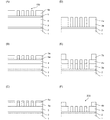
- a method for manufacturing the phase shift mask 200 according to the first embodiment will be described below according to the manufacturing process shown in FIG.
- phase shift mask 200 using the mask blank 100 in which the hard mask film 5 is laminated on the light shielding film 4 will be described.
- a material containing chromium is applied to the light shielding film 4 and a material containing silicon is applied to the hard mask film 5 will be described.
- a resist film is formed by a spin coating method in contact with the hard mask film 5 in the mask blank 100.
- a first pattern which is a transfer pattern (phase shift pattern) to be formed on the phase shift film 3 is drawn on the resist film with an electron beam, and further, a predetermined process such as a development process is performed, so that the phase A first resist pattern 6a having a shift pattern is formed (see FIG. 3A).
- dry etching using a fluorine-based gas is performed using the first resist pattern 6a as a mask to form a first pattern (hard mask pattern 5a) on the hard mask film 5 (see FIG. 3B).
- dry etching using a mixed gas of chlorine-based gas and oxygen gas is performed using the hard mask pattern 5a as a mask to form the first pattern (light-shielding pattern 4a) on the light-shielding film 4.
- dry etching using a fluorine-based gas is performed using the light-shielding pattern 4a as a mask to form the first pattern (phase shift pattern 3a) on the phase shift film 3, and at the same time, the hard mask pattern 5a is also removed ( (See FIG. 3D).
- phase shift film 3 During dry etching of the phase shift film 3 with a fluorine-based gas, additional etching (overover) is performed in order to increase the perpendicularity of the pattern side wall of the phase shift pattern 3a and to increase CD uniformity in the plane of the phase shift pattern 3a. Etching). Even after the over-etching, the surface of the etching stopper film 2 is finely etched, and the surface of the translucent substrate 1 is not exposed in the translucent part of the phase shift pattern 3a.
- a resist film is formed on the mask blank 100 by a spin coating method.
- a second pattern which is a pattern to be formed on the light-shielding film 4 (light-shielding pattern)
- a predetermined process such as a development process is further performed to provide a second pattern having a light-shielding pattern.
- the resist pattern 7b is formed (see FIG. 3E).
- the second pattern is a relatively large pattern, exposure drawing using laser light by a high-throughput laser drawing apparatus can be used instead of drawing using an electron beam.
- etching using a mixed gas of chlorine-based gas and oxygen gas is performed using the second resist pattern 7b as a mask to form a second pattern (light-shielding pattern 4b) on the light-shielding film 4.
- the second resist pattern 7b is removed, and a phase shift mask 200 is obtained through a predetermined process such as cleaning (see FIG. 3F).
- a phase shift mask 200 is obtained through a predetermined process such as cleaning (see FIG. 3F).
- a predetermined process such as cleaning (see FIG. 3F).
- cleaning process ammonia perhydration was used, but the surface of the etching stopper film 2 was hardly dissolved, and the surface of the translucent substrate 1 was not exposed in the translucent part of the phase shift pattern 3a.
- the chlorine-based gas used in the dry etching is not particularly limited as long as it contains chlorine (Cl).
- Cl chlorine
- SiCl 2 CHCl 3, CH 2 Cl 2, BCl 3
- the fluorine-based gas used in the dry etching is not particularly limited as long as it contains fluorine (F). Absent. For example, CHF 3, CF 4, C 2 F 6, C 4 F 8, SF 6 , and the like.
- the phase shift mask 200 of the first embodiment is manufactured using the mask blank 100 described above.
- the etching stopper film 2 has higher resistance to dry etching by a fluorine-based gas performed when forming a pattern on the phase shift film 3 than that of a translucent substrate, high resistance to chemical cleaning, and transmittance to exposure light. It satisfies the three characteristics of high at the same time. Accordingly, when the phase shift pattern (transfer pattern) 3a is formed on the phase shift film 3 by dry etching using a fluorine-based gas, overetching can be performed without digging the main surface of the translucent substrate 1.
- the phase shift mask 200 according to the first embodiment has high side wall perpendicularity of the phase shift pattern 3a and high CD uniformity within the surface of the phase shift pattern 3a. Further, during the manufacturing process of the phase shift mask 200, a black defect is found in the phase shift pattern 3a, and when the black defect is corrected by EB defect correction, the etching end point is easily detected, so the black defect is corrected with high accuracy. can do.
- the semiconductor device manufacturing method uses the phase shift mask 200 manufactured using the phase shift mask 200 according to the first embodiment or the mask blank 100 according to the first embodiment, and a resist film on the semiconductor substrate.
- the transfer pattern is exposed and transferred.
- the phase shift mask 200 according to the first embodiment has high sidewall verticality of the phase shift pattern 3a and high CD uniformity within the surface of the phase shift pattern 3a. For this reason, when the phase shift mask 200 of Embodiment 1 is used for exposure transfer onto a resist film on a semiconductor device, a pattern can be formed on the resist film on the semiconductor device with sufficient accuracy to satisfy the design specifications.
- the black defect portion is exposed and transferred to the resist film on the semiconductor device using the phase shift mask in which the black defect portion is corrected by EB defect correction during the manufacturing process, the black defect is corrected with high accuracy. It is possible to prevent a transfer failure from occurring in the resist film on the semiconductor device corresponding to the pattern portion where the black defects existed. For this reason, when a circuit pattern is formed by dry etching the film to be processed using this resist pattern as a mask, a high-accuracy and high-yield circuit pattern without wiring short-circuits or disconnections due to insufficient accuracy or transfer failure is formed. be able to.
- the mask blank according to the second embodiment of the present invention is such that a pattern forming thin film is a light-shielding film having a predetermined optical density, and includes a binary mask (transfer mask), a digging Levenson type phase shift mask (transfer). This is used for manufacturing a CPL (Chromeless Phase Lithography) mask (transfer mask).
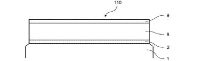
- FIG. 4 shows the configuration of the mask blank of the second embodiment.
- the mask blank 110 according to the second embodiment has a structure in which an etching stopper film 2, a light shielding film (thin film for pattern formation) 8, and a hard mask film 9 are sequentially laminated on a translucent substrate 1.
- symbol is used and description here is abbreviate
- the light shielding film 8 is a pattern forming thin film on which a transfer pattern is formed when a binary mask is manufactured from a mask blank.
- the binary mask is required to have high light shielding performance for the pattern of the light shielding film 8.
- the OD with respect to the exposure light is required to be 2.8 or more with only the light shielding film 8, and more preferably 3.0 or more.
- the light shielding film 8 can be applied to either a single layer structure or a laminated structure of two or more layers.
- each layer of the light shielding film having a single layer structure and the light shielding film having a laminated structure of two or more layers has a composition gradient in the thickness direction of the layer even if the layers have almost the same composition in the film thickness direction. It may be a configuration.
- the light shielding film 8 is formed of a material capable of patterning a transfer pattern by dry etching with a fluorine-based gas.
- the material having such characteristics include a material containing a transition metal and silicon in addition to a material containing silicon.
- the material containing a transition metal and silicon has a higher light shielding performance than a material containing silicon that does not contain a transition metal, and the thickness of the light shielding film 8 can be reduced.
- transition metals to be contained in the light shielding film 8 molybdenum (Mo), tantalum (Ta), tungsten (W), titanium (Ti), chromium (Cr), hafnium (Hf), nickel (Ni), vanadium (V) , Zirconium (Zr), ruthenium (Ru), rhodium (Rh), niobium (Nb), palladium (Pd), or any one metal or an alloy of these metals.
- Mo molybdenum
- Ta tantalum
- Ti tungsten
- Ti titanium
- Cr chromium
- Hf hafnium
- Ni nickel
- the light shielding film 8 does not contain aluminum.
- the light shielding film 8 is formed of a material containing silicon
- a metal other than a transition metal such as tin (Sn) indium (In) or gallium (Ga)
- the etching selectivity of the dry etching with the fluorine-based gas between the etching stopper film 2 may be lowered, and the EB defect correction for the light shielding film 8 may be performed. When this is done, it may be difficult to detect the etching end point.
- the light shielding film 8 can be formed of a material containing silicon and nitrogen, or a material containing one or more elements selected from a metalloid element, a nonmetallic element, and a rare gas in a material consisting of silicon and nitrogen.
- the light shielding film 8 may contain any metalloid element.
- inclusion of one or more elements selected from boron, germanium, antimony and tellurium is expected to improve the conductivity of silicon used as a target when the light shielding film 8 is formed by sputtering. This is preferable because it is possible.
- the lower layer is formed of a material made of silicon or a material containing one or more elements selected from silicon, carbon, boron, germanium, antimony, and tellurium.
- the light shielding film 8 may be formed of a material containing tantalum.
- the silicon content of the light shielding film 8 is preferably 5 atomic% or less, more preferably 3 atomic% or less, and even more preferably substantially not contained.
- These tantalum-containing materials are materials capable of patterning a transfer pattern by dry etching using a fluorine-based gas.
- the material containing tantalum in this case include a material in which tantalum contains one or more elements selected from nitrogen, oxygen, boron, and carbon in addition to tantalum metal. Examples thereof include Ta, TaN, TaO, TaON, TaBN, TaBO, TaBON, TaCN, TaCO, TaCON, TaBCN, TaBOCN, and the like.
- the material for forming the light-shielding film 8 may contain one or more elements selected from oxygen, nitrogen, carbon, boron, and hydrogen as long as the optical density is not significantly reduced.
- the surface layer opposite to the translucent substrate 1 in the case of a two-layer structure of a lower layer and an upper layer
- the upper layer may contain a large amount of oxygen or nitrogen.
- the hard mask film 9 is provided on the light shielding film 8.
- the hard mask film 9 needs to be formed of a material having etching selectivity with respect to an etching gas used when the light shielding film 8 is etched. Thereby, the thickness of the resist film can be significantly reduced as compared with the case where the resist film is directly used as a mask for the light shielding film 8.
- the light-shielding film 8 needs to have a sufficient light-shielding function by securing a predetermined optical density.
- the hard mask film 9 it is sufficient for the hard mask film 9 to have a film thickness that can function as an etching mask until dry etching for forming a pattern on the light shielding film 8 immediately below is completed. Not subject to restrictions. For this reason, the thickness of the hard mask film 9 can be made much thinner than the thickness of the light shielding film 8.
- the resist film made of an organic material only needs to have a thickness sufficient to function as an etching mask until the dry etching for forming a pattern on the hard mask film 9 is completed.
- the film thickness of the resist film can be made much thinner than when it is directly used as the mask No. 8. Since the resist film can be thinned in this way, the resist resolution can be improved and the formed pattern can be prevented from collapsing.
- the hard mask film 9 is preferably formed of a material containing chromium.
- the hard mask film 9 is more preferably formed of a material containing one or more elements selected from nitrogen, oxygen, carbon, hydrogen and boron in addition to chromium.
- the hard mask film 9 includes at least one metal element selected from indium (In), tin (Sn), and molybdenum (Mo) (hereinafter referred to as “metal such as indium”). It may be formed of a material containing “element”.
- a resist film made of an organic material is formed with a film thickness of 100 nm or less in contact with the surface of the hard mask film 9.
- a transfer pattern (phase shift pattern) to be formed on the hard mask film 9 may be provided with SRAF (Sub-Resolution Assist Feature) having a line width of 40 nm.
- SRAF Sub-Resolution Assist Feature
- the cross-sectional aspect ratio of the resist pattern is as low as 1: 2.5, it is possible to suppress the resist pattern from collapsing or detaching during development or rinsing of the resist film.
- the film thickness of the resist film is 80 nm or less because collapse and detachment of the resist pattern are further suppressed.
- the mask blank 110 of the second embodiment includes the etching stopper film 2 containing silicon, aluminum, and oxygen between the translucent substrate 1 and the light shielding film 8 that is a pattern forming thin film.
- the etching stopper film 2 has higher resistance to dry etching with a fluorine-based gas performed when forming a pattern on the light-shielding film 8 than the translucent substrate 1 and has higher resistance to chemical cleaning, and is resistant to exposure light. It satisfies the three characteristics of high transmittance at the same time.
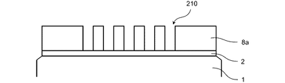
- the etching stopper film 2 of the mask blank 110 is left on the entire main surface of the translucent substrate 1, and the transfer pattern ( A light-shielding pattern 8a) is formed.
- the hard mask film 9 is removed during the production of the transfer mask 210.
- the transfer mask 210 includes a light-shielding pattern 8a that is a light-shielding film having a transfer pattern on the main surface of the light-transmitting substrate 1, and the light-transmitting substrate 1 and the light-shielding pattern 8a.
- An etching stopper film 2 is provided therebetween, the light shielding pattern 8a contains silicon, and the etching stopper film 2 contains silicon, aluminum, and oxygen.
- the method for manufacturing a transfer mask (binary mask) according to the second embodiment uses the mask blank 110, and forms a transfer pattern on the light shielding film 8 by dry etching using a fluorine-based gas. It is characterized by comprising a process.
- a method for manufacturing the transfer mask 210 according to the second embodiment will be described below in accordance with the manufacturing process shown in FIG.
- a method for manufacturing the transfer mask 210 using the mask blank 110 in which the hard mask film 9 is laminated on the light shielding film 8 will be described.
- a material containing a transition metal and silicon is applied to the light shielding film 8 and a material containing chromium is applied to the hard mask film 9 will be described.
- a resist film is formed by spin coating in contact with the hard mask film 9 in the mask blank 110.
- a transfer pattern (light-shielding pattern) to be formed on the light-shielding film 8 is drawn on the resist film with an electron beam, and a predetermined process such as a development process is performed to form a resist pattern 10a having the light-shielding pattern. (See FIG. 6A).
- dry etching using a mixed gas of chlorine-based gas and oxygen gas is performed using the resist pattern 10a as a mask to form a transfer pattern (hard mask pattern 9a) on the hard mask film 9 (see FIG. 6B). ).
- dry etching using fluorine gas is performed using the hard mask pattern 9a as a mask to form a transfer pattern (light shielding pattern 8a) on the light shielding film 8 (FIG. 6C). reference).
- additional etching is performed to increase the verticality of the pattern sidewall of the light shielding pattern 8a and to improve CD uniformity within the surface of the light shielding pattern 8a. Is going.
- the surface of the etching stopper film 2 is finely etched, and the surface of the translucent substrate 1 is not exposed even in the translucent portion of the light shielding pattern 8a.
- the remaining hard mask pattern 9a is removed by dry etching using a mixed gas of chlorine-based gas and oxygen gas, and a transfer mask 210 is obtained through a predetermined process such as cleaning (see FIG. 6D).
- a predetermined process such as cleaning (see FIG. 6D).
- ammonia perwater was used, but the surface of the etching stopper film 2 was hardly dissolved, and the surface of the translucent substrate 1 was not exposed in the translucent portion of the light shielding pattern 8a.
- the chlorine-based gas and fluorine-based gas used in the dry etching are the same as those used in the first embodiment.
- the transfer mask 210 according to the second embodiment is manufactured using the mask blank 110 described above.
- the etching stopper film 2 has higher resistance to dry etching with a fluorine-based gas performed when forming a pattern on the light-shielding film 8, higher resistance to chemical cleaning, and higher transmittance to exposure light. These three characteristics are satisfied at the same time.
- the transfer mask 210 of the second embodiment has a high verticality of the side wall of the light shielding pattern 8a and a high CD uniformity within the surface of the light shielding pattern 8a.
- a black defect is found in the light shielding pattern 8a, and when the black defect is corrected by EB defect correction, the etching end point can be easily detected, so the black defect is corrected with high accuracy. be able to.
- the semiconductor device manufacturing method of the second embodiment uses a transfer mask 210 manufactured by using the transfer mask 210 of the second embodiment or the mask blank 110 of the second embodiment, and forms a resist film on a semiconductor substrate.
- the transfer pattern is exposed and transferred.
- the transfer mask 200 according to the second embodiment has high verticality of the side wall of the light shielding pattern 8a and high CD uniformity within the surface of the light shielding pattern 8a. For this reason, when exposure transfer is performed on the resist film on the semiconductor device using the transfer mask 210 of the second embodiment, a pattern can be formed on the resist film on the semiconductor device with sufficient accuracy to satisfy the design specifications.
- Example 1 Manufacture of mask blanks
- a translucent substrate 1 made of synthetic quartz glass having a main surface dimension of about 152 mm ⁇ about 152 mm and a thickness of about 6.35 mm was prepared.
- the translucent substrate 1 has its end face and main surface polished to a predetermined surface roughness or less (root mean square roughness Rq of 0.2 nm or less), and then subjected to a predetermined cleaning process and drying process. It is.
- an etching stopper film 2 (AlSiO film) made of aluminum, silicon, and oxygen was formed in a thickness of 10 nm in contact with the surface of the translucent substrate 1.
- the translucent substrate 1 is installed in a single wafer RF sputtering apparatus, an Al 2 O 3 target and a SiO 2 target are simultaneously discharged, and sputtering using an argon (Ar) gas as a sputtering gas (RF sputtering).
- Ar argon
- RF sputtering a sputtering gas
- Si / [Si + Al] of the etching stopper film 2 is 0.475.
- numerical correction is performed based on the result of RBS analysis (analysis by Rutherford backscattering method) (the same applies to the following analysis).
- the refractive index n was 1.625 and the extinction coefficient k was 193 nm for light having a wavelength of 193 nm.
- the refractive index n was 1.625
- the extinction coefficient k was 193 nm for light having a wavelength of 193 nm.
- phase shift film (MoSiN film) 3 made of molybdenum, silicon, and nitrogen was formed in a thickness of 64 nm in contact with the surface of the etching stopper film 2.
- the translucent substrate 1 after the etching stopper film 2 is formed in a single wafer DC sputtering apparatus is installed, and a mixed sintered target (Mo: Mo) of molybdenum (Mo) and silicon (Si).
- phase shift film 3 was formed by reactive sputtering (DC sputtering) using 0.2 Pa) as a sputtering gas.
- Mo: Si: N 4.1-35.6: 60.3 (atomic % Ratio).
- the light-transmitting substrate 1 after the phase shift film 3 was formed was heat-treated in the atmosphere. This heat treatment was performed at 450 ° C. for 30 minutes.
- the transmittance and the phase shift amount at the wavelength (193 nm) of the ArF excimer laser were measured with the phase shift amount measuring device MPM193 (manufactured by Lasertec Corporation) for the phase shift film 3 after the heat treatment, the transmittance was 7. It was 35% and the phase shift amount was 162 degrees.
- phase shift film formed on another light-transmitting substrate under the same conditions and subjected to heat treatment is subjected to a phase shift film using a spectroscopic ellipsometer (M-2000D manufactured by JA Woollam).
- M-2000D manufactured by JA Woollam
- a light shielding film (CrOCN film) 4 made of chromium, oxygen, carbon, and nitrogen was formed in a thickness of 46 nm in contact with the surface of the phase shift film 3.
- the translucent substrate 1 after the heat treatment is installed in a single wafer DC sputtering apparatus, and using a chromium (Cr) target, argon (Ar), carbon dioxide (CO 2 ), and nitrogen (N 2 ).
- helium (He) as a sputtering gas
- the light-shielding film 4 was formed by reactive sputtering (DC sputtering).
- a hard mask film (SiON film) 5 made of silicon, oxygen, and nitrogen was formed in a thickness of 5 nm in contact with the surface of the light shielding film 4.
- the translucent substrate 1 after the light-shielding film 4 is formed in a single wafer DC sputtering apparatus is installed, and a silicon (Si) target is used, and argon (Ar) and nitrogen monoxide (NO) are used.
- He helium
- the transmittance of the etching stopper film formed on another light-transmitting substrate at the wavelength of ArF excimer laser (193 nm) was measured with the above-described phase shift measuring apparatus, and the transmittance of the light-transmitting substrate was 100%.
- the transmittance was 98.3%, and it was found that the effect of the decrease in transmittance caused by providing the etching stopper film of Example 1 was small.
- the translucent substrate on which the etching stopper film was formed was immersed in ammonia water having a concentration of 0.5%, and the etching rate was measured. As a result, it was 0.1 nm / min. From this result, it was confirmed that the etching stopper film 2 of Example 1 has sufficient resistance to chemical cleaning performed in the process of manufacturing the phase shift mask from the mask blank.
- Etching gas mixture of SF 6 and He for each of another translucent substrate, an etching stopper film formed on another translucent substrate, and a phase shift film formed on another translucent substrate The dry etching used in was performed under the same conditions. Then, each etching rate was calculated, and an etching selectivity between the three was calculated.
- the etching selectivity of the etching stopper film of Example 1 with respect to the etching rate of the translucent substrate was 0.1.
- the etching selectivity of the phase shift film of Example 1 with respect to the etching rate of the translucent substrate was 2.38.
- the etching selectivity of the phase shift film of Example 1 to the etching rate of the etching stopper film of Example 1 was 23.8.
- phase shift mask 200 of Example 1 was produced according to the following procedure. First, the surface of the hard mask film 5 was subjected to HMDS treatment. Subsequently, a resist film made of a chemically amplified resist for electron beam drawing was formed in a thickness of 80 nm in contact with the surface of the hard mask film 5 by spin coating. Next, a first pattern which is a phase shift pattern to be formed on the phase shift film 3 is drawn on the resist film by electron beam, a predetermined development process is performed, and the first resist having the first pattern is formed. A pattern 6a was formed (see FIG. 3A). At this time, in the first pattern drawn by the electron beam, a program defect was added in addition to the phase shift pattern to be originally formed so that a black defect was formed in the phase shift film.
- a resist film made of a chemically amplified resist for electron beam drawing was formed on the light-shielding pattern 4a by spin coating so as to have a film thickness of 150 nm.
- a second pattern which is a pattern (light-shielding pattern) to be formed on the light-shielding film 4 is drawn on the resist film, and a predetermined process such as a development process is further performed, so that the second resist having the light-shielding pattern is obtained.
- a pattern 7b was formed (see FIG. 3E).
- phase shift mask When a phase shift mask was manufactured in the same procedure using another mask blank and the CD uniformity in the plane of the phase shift pattern was inspected, it was a satisfactory result. Further, when the cross section of the phase shift pattern was observed with a STEM, the perpendicularity of the side wall of the phase shift pattern was high, the etching stopper film was as small as less than 1 nm, and no microtrench was generated.
- Example 2 Manufacture of mask blanks
- the mask blank of Example 2 is manufactured in the same manner as the mask blank of Example 1 except for the etching stopper film 2, the phase shift film 3, and the hard mask film 5.
- the difference from the mask blank of Example 1 will be described.
- the etching stopper film 2 has a refractive index n of 1.600 and an extinction coefficient k of 0.000 (lower measurement limit) for light having a wavelength of 193 nm.
- the phase shift film 3 of Example 2 has a structure in which a low transmission layer, a high transmission layer, and an uppermost layer are laminated in contact with the surface of the etching stopper film 2.
- a specific film forming process is as follows. A translucent substrate 1 on which an etching stopper film 2 is formed is installed in a single wafer RF sputtering apparatus, and a mixed gas (flow rate ratio Ar) of argon (Ar) and nitrogen (N 2 ) using a silicon (Si) target.
- RF sputtering reactive sputtering
- the translucent substrate 1 on which the low transmission layer is laminated is installed in a single wafer RF sputtering apparatus, and a mixed gas of argon (Ar) and nitrogen (N 2 ) using a silicon (Si) target (
- the refractive index n at a wavelength of 193 nm was obtained.
- the extinction coefficient k was 0.39.
- the hard mask film (SiO 2 film Si: O 33: 67 (atomic% ratio)) 5 made of silicon and oxygen is in contact with the surface of the light shielding film 4 to a thickness of 5 nm. Formed with.
- the transmittance of the etching stopper film formed on another translucent substrate at the wavelength of ArF excimer laser (193 nm) was measured with the above-described phase shift amount measuring apparatus.
- the transmissivity of the translucent substrate was set to 100%.
- the transmittance at the time was 99.4%, and it was found that the influence of the decrease in transmittance caused by providing the etching stopper film of this Example 2 was small.
- the etching rate was measured by immersing the translucent substrate on which the etching stopper film was formed in ammonia water having a concentration of 0.5%, it was 0.1 nm / min. From this result, it was confirmed that the etching stopper film 2 of Example 2 has sufficient resistance to chemical cleaning performed in the process of manufacturing the phase shift mask from the mask blank.
- Etching gas mixture of SF 6 and He for each of another translucent substrate, an etching stopper film formed on another translucent substrate, and a phase shift film formed on another translucent substrate The dry etching used in was performed under the same conditions. Then, each etching rate was calculated, and an etching selectivity between the three was calculated.
- the etching selectivity of the etching stopper film of Example 2 with respect to the etching rate of the translucent substrate was 0.2.
- the etching selectivity of the phase shift film of Example 2 with respect to the etching rate of the translucent substrate was 2.03.
- the etching selectivity of the phase shift film of Example 2 to the etching rate of the etching stopper film of Example 2 was 10.15.
- phase shift mask 200 of Example 2 was produced in the same procedure as in Example 1.
- the mask pattern was inspected by the mask inspection apparatus with respect to the produced halftone phase shift mask 200 of Example 2
- a black defect was confirmed in the phase shift pattern 3a where the program defect was placed.
- the etching end point can be easily detected, and the etching on the surface of the etching stopper film 2 can be minimized. did it.
- phase shift mask was manufactured in the same procedure, and in-plane CD uniformity of the phase shift pattern was inspected. Further, when the cross section of the phase shift pattern was observed with a STEM, the perpendicularity of the side wall of the phase shift pattern was high, the depth of the etching stopper film was as small as less than 1 nm, and no microtrench was generated.
- Example 3 Manufacture of mask blanks
- the mask blank of Example 3 is manufactured in the same manner as the mask blank of Example 2 except for the etching stopper film 2.
- the surface of the translucent substrate 1 is applied.
- the etching stopper film 2 has a refractive index n of 1.589 and an extinction coefficient k of 0.000 (lower measurement limit) in light having a wavelength of 193 nm.
- the transmittance of the etching stopper film formed on another translucent substrate at the wavelength of ArF excimer laser (193 nm) was measured with the above-described phase shift amount measuring apparatus.
- the transmissivity of the translucent substrate was set to 100%.
- the transmittance was 99.8%, and it was found that the effect of the decrease in transmittance caused by providing the etching stopper film of Example 3 was small.
- the etching rate was measured by immersing the translucent substrate on which the etching stopper film was formed in ammonia water having a concentration of 0.5%, it was 0.1 nm / min. From this result, it was confirmed that the etching stopper film 2 of Example 3 has sufficient resistance to chemical cleaning performed in the process of manufacturing the phase shift mask from the mask blank.
- Etching gas mixture of SF 6 and He for each of another translucent substrate, an etching stopper film formed on another translucent substrate, and a phase shift film formed on another translucent substrate The dry etching used in was performed under the same conditions. Then, each etching rate was calculated, and an etching selectivity between the three was calculated.
- the etching selectivity of the etching stopper film of Example 3 with respect to the etching rate of the translucent substrate was 0.34.
- the etching selectivity of the phase shift film of Example 3 with respect to the etching rate of the translucent substrate was 2.03.
- the etching selectivity of the phase shift film of Example 3 to the etching rate of the etching stopper film of Example 3 was 5.97.
- phase shift mask 200 of Example 3 was produced in the same procedure as in Example 1.
- the mask pattern was inspected by the mask inspection apparatus with respect to the manufactured halftone phase shift mask 200 of Example 3, a black defect was confirmed in the phase shift pattern 3a where the program defect was arranged.
- the EB defect correction using an electron beam and XeF 2 gas is performed on the black defect portion, the etching end point can be easily detected, and the etching on the surface of the etching stopper film 2 can be minimized. did it.
- phase shift mask was manufactured in the same procedure, and in-plane CD uniformity of the phase shift pattern was inspected. Further, when the cross section of the phase shift pattern was observed with a STEM, the perpendicularity of the side wall of the phase shift pattern was high, the depth of the etching stopper film was as small as about 1 nm, and no microtrench was generated.
- Example 4 Manufacture of mask blanks
- the mask blank of Example 4 is manufactured in the same manner as the mask blank of Example 2 except for the etching stopper film 2.
- the etching stopper film 2 has a refractive index n of 1.720 and an extinction coefficient k of 0.032 in light having a wavelength of 193 nm.
- the transmittance of the etching stopper film formed on another translucent substrate at the wavelength of ArF excimer laser (193 nm) was measured with the above-described phase shift amount measuring apparatus.
- the transmissivity of the translucent substrate was set to 100%.
- the transmittance at the time was 95.2%, and it was found that the influence of the decrease in transmittance caused by providing the etching stopper film of Example 4 was small.
- the etching rate was measured by immersing the translucent substrate on which the etching stopper film was formed in ammonia water having a concentration of 0.5%, it was 0.2 nm / min. From this result, it was confirmed that the etching stopper film 2 of Example 4 has sufficient resistance to chemical cleaning performed in the process of manufacturing the phase shift mask from the mask blank.
- Etching gas mixture of SF 6 and He for each of another translucent substrate, an etching stopper film formed on another translucent substrate, and a phase shift film formed on another translucent substrate The dry etching used in was performed under the same conditions. Then, each etching rate was calculated, and an etching selectivity between the three was calculated.
- the etching selectivity of the etching stopper film of Example 4 with respect to the etching rate of the translucent substrate was 0.042.
- the etching selectivity of the phase shift film of Example 4 with respect to the etching rate of the translucent substrate was 2.03.
- the etching selectivity of the phase shift film of Example 4 to the etching rate of the etching stopper film of Example 4 was 48.3.
- phase shift mask 200 of Example 4 was produced in the same procedure as in Example 1.
- the mask pattern was inspected by the mask inspection apparatus with respect to the manufactured halftone phase shift mask 200 of Example 4
- a black defect was confirmed in the phase shift pattern 3a where the program defect was placed.
- the etching end point can be easily detected, and the etching on the surface of the etching stopper film 2 can be minimized. did it.
- phase shift mask was manufactured in the same procedure, and in-plane CD uniformity of the phase shift pattern was inspected. Further, when the cross section of the phase shift pattern was observed with a STEM, the perpendicularity of the side wall of the phase shift pattern was high, the depth of the etching stopper film was as small as less than 1 nm, and no microtrench was generated.
- Example 5 Manufacture of mask blanks
- the mask blank of Example 5 is for manufacturing a binary type mask (transfer mask).
- an etching stopper film 2 As shown in FIG. 4, an etching stopper film 2, a lower layer and an upper layer are formed on a translucent substrate 1. It has a structure in which a light shielding film 8 and a hard mask film 9 having a laminated structure are laminated.
- the difference from the mask blank of Example 1 will be described.
- the etching stopper film 2 of Example 5 is formed by the same procedure as that of the etching stopper film of Example 1, and its characteristics are equivalent to those of the etching stopper film of Example 1.
- a lower layer (MoSiN film) of the light shielding film 8 made of molybdenum, silicon and nitrogen is formed with a thickness of 47 nm
- an upper layer (MoSiN film) is formed with a thickness of 13 nm.
- the translucent substrate 1 after the etching stopper film 2 is formed in a single wafer DC sputtering apparatus is installed, and a mixed sintered target (Mo: Mo) of molybdenum (Mo) and silicon (Si).
- the translucent substrate 1 provided with the light shielding film 8 was subjected to a heat treatment at 450 ° C. for 30 minutes to reduce the film stress of the light shielding film 8.
- the analysis by X-ray photoelectron spectroscopy was performed with respect to the light shielding film which formed in another light-transmitting board
- nitrogen was 14.4 atomic% and oxygen was 38.3 atomic%. Moreover, it was 3.0 when the optical density of the light shielding film was measured using the said spectroscopic ellipsometer.
- a hard mask film 9 made of chromium and nitrogen was formed in a thickness of 5 nm in contact with the surface of the upper layer of the light shielding film 8.
- the translucent substrate 1 provided with the light-shielding film 8 after heat treatment is installed in a single-wafer DC sputtering apparatus, a chromium (Cr) target is used, and argon (Ar) and nitrogen (N 2 )
- the hard mask film 9 was formed by reactive sputtering (DC sputtering) using a mixed gas as a sputtering gas.
- the transmittance of the etching stopper film formed on another light-transmitting substrate at the wavelength of ArF excimer laser (193 nm) was measured with the above-described phase shift measuring apparatus, and the transmittance of the light-transmitting substrate was 100%.
- the transmittance was 98.3%, and it was found that the effect of the decrease in transmittance caused by providing the etching stopper film of Example 5 was small.
- the translucent substrate on which the etching stopper film was formed was immersed in ammonia water having a concentration of 0.5%, and the etching rate was measured. As a result, it was 0.1 nm / min. From this result, it was confirmed that the etching stopper film 2 of Example 5 has sufficient resistance to chemical cleaning performed in the process of manufacturing the transfer mask from the mask blank.
- a mixed gas of SF 6 and He is used as an etching gas for another light-transmitting substrate, an etching stopper film formed on another light-transmitting substrate, and a light-shielding film formed on another light-transmitting substrate.
- the dry etching used was performed under the same conditions. Then, each etching rate was calculated, and an etching selectivity between the three was calculated.
- the etching selectivity of the etching stopper film of Example 5 with respect to the etching rate of the translucent substrate was 0.1.
- the etching selectivity of the light shielding film of Example 5 with respect to the etching rate of the translucent substrate was 1.9.
- the etching selectivity of the light shielding film of Example 5 with respect to the etching rate of the etching stopper film of Example 5 was 19.0.
- a transfer mask 210 of Example 5 was produced in the following procedure. First, a resist film made of a chemically amplified resist for electron beam drawing was formed to a thickness of 80 nm in contact with the surface of the hard mask film 9 by spin coating. Next, a transfer pattern to be formed on the light-shielding film 8 was drawn on the resist film with an electron beam, and a predetermined development process was performed to form a resist pattern 10a (see FIG. 6A). At this time, a program defect was added to the pattern drawn by the electron beam in addition to the transfer pattern to be originally formed so that a black defect was formed in the light shielding film 8.
- the resist pattern 10a was removed by TMAH.
- dry etching using fluorine-based gas SF 6 + He
- SF 6 + He fluorine-based gas
- the etching time (just etching time) from the start of etching of the light shielding film 8 to the time when the etching proceeds in the thickness direction of the light shielding film 8 and the surface of the etching stopper film 2 begins to be exposed.
- additional etching was performed for 20% of the just etching time (overetching time). Note that this dry etching with a fluorine-based gas is biased with a power of 10 W, and was performed under so-called high bias etching conditions.
- a transfer mask was manufactured in the same procedure, and the CD uniformity within the surface of the light shielding pattern was inspected. Further, when the cross section of the light shielding pattern was observed with a STEM, the verticality of the side wall of the light shielding pattern was high, the depth of the etching stopper film was as small as less than 1 nm, and no microtrench was generated.
- the mask blank of Comparative Example 1 has the same configuration as the mask blank of Example 1 except that the etching stopper film 2 is formed of a material made of aluminum and oxygen.
- an etching stopper film 2 (AlO film) made of aluminum and oxygen was formed with a thickness of 10 nm in contact with the surface of the light-transmitting substrate 1.
- the translucent substrate 1 is installed in a single wafer RF sputtering apparatus, an etching stopper film is formed by sputtering (RF sputtering) using an Al 2 O 3 target and argon (Ar) gas as a sputtering gas. 2 was formed.
- the etching stopper film has a refractive index n of 1.864 and an extinction coefficient k of 0.069 in light having a wavelength of 193 nm.
- the transmittance of the etching stopper film formed on another translucent substrate at the wavelength of ArF excimer laser (193 nm) was measured with the above-described phase shift amount measuring apparatus.
- the transmissivity of the translucent substrate was set to 100%.
- the transmittance was 91.7%, and it was found that the influence of the decrease in transmittance caused by providing the etching stopper film of Comparative Example 1 was relatively large.
- the etching rate was measured by immersing the translucent substrate on which the etching stopper film was formed in ammonia water having a concentration of 0.5%, it was 4.0 nm / min. From this result, it can be seen that the etching stopper film 2 of Comparative Example 1 does not have sufficient resistance to chemical cleaning performed in the process of manufacturing the phase shift mask from the mask blank.
- Etching gas mixture of SF 6 and He for each of another translucent substrate, an etching stopper film formed on another translucent substrate, and a phase shift film formed on another translucent substrate The dry etching used in was performed under the same conditions. Then, each etching rate was calculated, and an etching selectivity between the three was calculated.
- the etching selectivity of the etching stopper film of Comparative Example 1 with respect to the etching rate of the translucent substrate was 0.025.
- the etching selectivity of the phase shift film of Comparative Example 1 with respect to the etching rate of the translucent substrate was 2.38.
- the etching selectivity of the phase shift film of Comparative Example 1 relative to the etching rate of the etching stopper film of Comparative Example 1 was 95.2.
- phase shift mask 200 of Comparative Example 1 was produced in the same procedure as in Example 1.
- the mask pattern was inspected by the mask inspection apparatus with respect to the manufactured halftone phase shift mask 200 of Comparative Example 1, many defects other than the program defects were detected.
- the phase shift pattern 3a being missing.
- the EB defect correction using the electron beam and XeF 2 gas was performed on the black defect portion where the program defect was arranged, the etching end point can be easily detected, and the surface of the etching stopper film 2 can be detected. It was possible to minimize etching.
- phase shift mask Using another mask blank, manufacture a phase shift mask in the same procedure, and observe the cross section of the phase shift pattern with STEM at the part where the phase shift pattern is not dropped. It was confirmed that dissolution of the etching stopper film immediately below the region where the phase shift pattern exists was also progressing from the side wall side to the inside of the phase shift pattern. From this result, it can be inferred that the fact that the etching stopper film was dissolved by the chemical cleaning was a cause of frequent dropout of the phase shift pattern.
Landscapes
- Physics & Mathematics (AREA)
- General Physics & Mathematics (AREA)
- Engineering & Computer Science (AREA)
- Plasma & Fusion (AREA)
- Preparing Plates And Mask In Photomechanical Process (AREA)
Abstract
Description
(構成1)
透光性基板の主表面上にパターン形成用薄膜を備えたマスクブランクであって、
前記パターン形成用薄膜は、ケイ素を含有し、
前記透光性基板と前記パターン形成用薄膜の間にエッチングストッパー膜を有し、
前記エッチングストッパー膜は、ケイ素、アルミニウムおよび酸素を含有することを特徴とするマスクブランク。
前記エッチングストッパー膜は、酸素含有量が60原子%以上であることを特徴とする構成1記載のマスクブランク。
前記エッチングストッパー膜は、前記ケイ素および前記アルミニウムの合計含有量に対する前記ケイ素の含有量の原子%による比率が、4/5以下であることを特徴とする構成1または2記載のマスクブランク。
前記エッチングストッパー膜は、ケイ素、アルミニウムおよび酸素からなることを特徴とする構成1から3のいずれかに記載のマスクブランク。
前記エッチングストッパー膜は、前記透光性基板の主表面に接して形成されていることを特徴とする構成1から4のいずれかに記載のマスクブランク。
前記エッチングストッパー膜は、厚さが3nm以上であることを特徴とする構成1から5のいずれかに記載のマスクブランク。
前記パターン形成用薄膜は、ケイ素および窒素を含有することを特徴とする構成1から6のいずれかに記載のマスクブランク。
前記パターン形成用薄膜は、遷移金属、ケイ素および窒素を含有することを特徴とする構成1から6のいずれかに記載のマスクブランク。
前記パターン形成用薄膜は、位相シフト膜であることを特徴とする構成1から8のいずれかに記載のマスクブランク。
前記位相シフト膜は、露光光を1%以上の透過率で透過させる機能と、前記位相シフト膜を透過した前記露光光に対して前記位相シフト膜の厚さと同じ距離だけ空気中を通過した前記露光光との間で150度以上180度以下の位相差を生じさせる機能とを有することを特徴とする構成9記載のマスクブランク。
前記位相シフト膜上に、遮光膜を備えることを特徴とする構成9または10に記載のマスクブランク。
構成1から8のいずれかに記載のマスクブランクの前記パターン形成用薄膜に転写パターンを有することを特徴とする転写用マスク。
構成11記載のマスクブランクの前記位相シフト膜に転写パターンを有し、前記遮光膜に遮光帯を含むパターンを有することを特徴とする転写用マスク。
構成1から8のいずれかに記載のマスクブランクを用いた転写用マスクの製造方法であって、
ドライエッチングにより前記パターン形成用薄膜に転写パターンを形成する工程を備えることを特徴とする転写用マスクの製造方法。
構成11記載のマスクブランクを用いた転写用マスクの製造方法であって、
ドライエッチングにより前記遮光膜に転写パターンを形成する工程と、
前記転写パターンを有する遮光膜をマスクとし、フッ素系ガスを用いるドライエッチングにより前記位相シフト膜に転写パターンを形成する工程と、
ドライエッチングにより前記遮光膜に遮光帯を含むパターンを形成する工程と
を備えることを特徴とする転写用マスクの製造方法。
構成12または13に記載の転写用マスクを用い、半導体基板上のレジスト膜に転写パターンを露光転写する工程を備えることを特徴とする半導体デバイスの製造方法。
構成14または15に記載の転写用マスクの製造方法により製造された転写用マスクを用い、半導体基板上のレジスト膜に転写パターンを露光転写する工程を備えることを特徴とする半導体デバイスの製造方法。
[マスクブランクとその製造]
本発明の第1の実施形態に係るマスクブランクは、パターン形成用薄膜を露光光に対して所定の透過率と位相差を付与する膜である位相シフト膜としたものであり、位相シフトマスク(転写用マスク)を製造するために用いられるものである。図1に、この第1の実施形態のマスクブランクの構成を示す。この第1の実施形態に係るマスクブランク100は、透光性基板1の主表面上に、エッチングストッパー膜2、位相シフト膜(パターン形成用薄膜)3、遮光膜4、ハードマスク膜5を備えている。
この第1の実施形態に係る位相シフトマスク200(図2参照)は、マスクブランク100のエッチングストッパー膜2は透光性基板1の主表面上の全面で残され、位相シフト膜3に転写用パターン(位相シフトパターン3a)が形成され、遮光膜4に遮光帯を含むパターン(遮光パターン4b:遮光帯、遮光パッチ等)が形成されていることを特徴としている。マスクブランク100にハードマスク膜5が設けられている構成の場合、この位相シフトマスク200の作製途上でハードマスク膜5は除去される。
実施の形態1の半導体デバイスの製造方法は、実施の形態1の位相シフトマスク200または実施の形態1のマスクブランク100を用いて製造された位相シフトマスク200を用い、半導体基板上のレジスト膜に転写用パターンを露光転写することを特徴としている。実施の形態1の位相シフトマスク200は、位相シフトパターン3aの側壁の垂直性が高く、位相シフトパターン3aの面内のCD均一性も高い。このため、実施の形態1の位相シフトマスク200を用いて半導体デバイス上のレジスト膜に露光転写すると、半導体デバイス上のレジスト膜に設計仕様を十分に満たす精度でパターンを形成することができる。
[マスクブランクとその製造]
本発明の第2の実施形態に係るマスクブランクは、パターン形成用薄膜を所定の光学濃度を有する遮光膜としたものであり、バイナリ型マスク(転写用マスク)、堀込レベンソン型位相シフトマスク(転写用マスク)、あるいはCPL(Chromeless Phase Lithography)マスク(転写用マスク)を製造するために用いられるものである。図4に、この第2の実施形態のマスクブランクの構成を示す。この第2の実施形態のマスクブランク110は、透光性基板1上に、エッチングストッパー膜2、遮光膜(パターン形成用薄膜)8、ハードマスク膜9が順に積層した構造からなるものである。なお、第1の実施形態のマスクブランクと同様の構成については同一の符号を使用し、ここでの説明を省略する。
この第2の実施形態に係る転写用マスク210(図5参照)は、マスクブランク110のエッチングストッパー膜2は透光性基板1の主表面上の全面で残され、遮光膜8に転写パターン(遮光パターン8a)が形成されていることを特徴としている。マスクブランク110にハードマスク膜9が設けられている構成の場合、この転写用マスク210の作製途上でハードマスク膜9は除去される。
実施の形態2の半導体デバイスの製造方法は、実施の形態2の転写用マスク210または実施の形態2のマスクブランク110を用いて製造された転写用マスク210を用い、半導体基板上のレジスト膜に転写用パターンを露光転写することを特徴としている。実施の形態2の転写用マスク200は、遮光パターン8aの側壁の垂直性が高く、遮光パターン8aの面内のCD均一性も高い。このため、実施の形態2の転写用マスク210を用いて半導体デバイス上のレジスト膜に露光転写すると、半導体デバイス上のレジスト膜に設計仕様を十分に満たす精度でパターンを形成することができる。
(実施例1)
[マスクブランクの製造]
主表面の寸法が約152mm×約152mmで、厚さが約6.35mmの合成石英ガラスからなる透光性基板1を準備した。この透光性基板1は、端面および主表面を所定の表面粗さ以下(二乗平均平方根粗さRqで0.2nm以下)に研磨され、その後、所定の洗浄処理および乾燥処理を施されたものである。
次に、この実施例1のマスクブランク100を用い、以下の手順で実施例1の位相シフトマスク200を作製した。最初に、ハードマスク膜5の表面にHMDS処理を施した。続いて、スピン塗布法によって、ハードマスク膜5の表面に接して、電子線描画用化学増幅型レジストからなるレジスト膜を膜厚80nmで形成した。次に、このレジスト膜に対して、位相シフト膜3に形成すべき位相シフトパターンである第1のパターンを電子線描画し、所定の現像処理を行い、第1のパターンを有する第1のレジストパターン6aを形成した(図3(A)参照)。なお、このとき電子線描画した第1のパターンには、位相シフト膜に黒欠陥が形成されるように、本来形成されるべき位相シフトパターンの他にプログラム欠陥を加えておいた。
[マスクブランクの製造]
この実施例2のマスクブランクは、エッチングストッパー膜2、位相シフト膜3、ハードマスク膜5を除いて、実施例1のマスクブランクと同様にして製造されるものである。以下、実施例1のマスクブランクと相違する箇所について説明する。
次に、この実施例2のマスクブランク100を用い、実施例1と同様の手順で実施例2の位相シフトマスク200を作製した。作製した実施例2のハーフトーン型の位相シフトマスク200に対してマスク検査装置によってマスクパターンの検査を行ったところ、プログラム欠陥を配置していた箇所の位相シフトパターン3aに黒欠陥が確認された。その黒欠陥部分に対し、電子線とXeF2ガスを用いるEB欠陥修正を行ったところ、エッチング終点を容易に検出することができ、エッチングストッパー膜2の表面へのエッチングを最小限にとどめることができた。
[マスクブランクの製造]
この実施例3のマスクブランクは、エッチングストッパー膜2を除いて、実施例2のマスクブランクと同様にして製造されるものである。この実施例3のエッチングストッパー膜2には、アルミニウム、ケイ素および酸素からなるAlSiO膜(Al:Si:O=7:28:65(原子%比))を適用し、透光性基板1の表面に接して、10nmの厚さで形成した。すなわち、このエッチングストッパー膜2のSi/[Si+Al]は、0.8である。また、このエッチングストッパー膜2の波長193nmの光における屈折率nは1.589、消衰係数kは0.000(測定下限)である。
次に、この実施例3のマスクブランク100を用い、実施例1と同様の手順で実施例3の位相シフトマスク200を作製した。作製した実施例3のハーフトーン型の位相シフトマスク200に対してマスク検査装置によってマスクパターンの検査を行ったところ、プログラム欠陥を配置していた箇所の位相シフトパターン3aに黒欠陥が確認された。その黒欠陥部分に対し、電子線とXeF2ガスを用いるEB欠陥修正を行ったところ、エッチング終点を容易に検出することができ、エッチングストッパー膜2の表面へのエッチングを最小限にとどめることができた。
[マスクブランクの製造]
この実施例4のマスクブランクは、エッチングストッパー膜2を除いて、実施例2のマスクブランクと同様にして製造されるものである。この実施例4のエッチングストッパー膜2には、アルミニウム、ケイ素および酸素からなるAlSiO膜(Al:Si:O=31:8:61(原子%比))を適用し、透光性基板1の表面に接して、10nmの厚さで形成した。すなわち、このエッチングストッパー膜2のSi/[Si+Al]は、0.205である。また、このエッチングストッパー膜2の波長193nmの光における屈折率nは1.720、消衰係数kは0.032である。
次に、この実施例4のマスクブランク100を用い、実施例1と同様の手順で実施例4の位相シフトマスク200を作製した。作製した実施例4のハーフトーン型の位相シフトマスク200に対してマスク検査装置によってマスクパターンの検査を行ったところ、プログラム欠陥を配置していた箇所の位相シフトパターン3aに黒欠陥が確認された。その黒欠陥部分に対し、電子線とXeF2ガスを用いるEB欠陥修正を行ったところ、エッチング終点を容易に検出することができ、エッチングストッパー膜2の表面へのエッチングを最小限にとどめることができた。
[マスクブランクの製造]
この実施例5のマスクブランクは、バイナリ型マスク(転写用マスク)を製造するためのものであり、図4に示すように、透光性基板1上に、エッチングストッパー膜2、下層および上層の積層構造からなる遮光膜8、ハードマスク膜9が積層した構造を備える。以下、実施例1のマスクブランクと相違する箇所について説明する。
次に、この実施例5のマスクブランク110を用い、以下の手順で実施例5の転写用マスク210を作製した。最初に、スピン塗布法によってハードマスク膜9の表面に接して、電子線描画用化学増幅型レジストからなるレジスト膜を膜厚80nmで形成した。次に、このレジスト膜に対して、遮光膜8に形成すべき転写パターンを電子線描画し、所定の現像処理を行い、レジストパターン10aを形成した(図6(A)参照)。なお、このとき電子線描画したパターンには、遮光膜8に黒欠陥が形成されるように、本来形成されるべき転写パターンの他にプログラム欠陥を加えておいた。
[マスクブランクの製造]
比較例1のマスクブランクは、エッチングストッパー膜2をアルミニウムと酸素からなる材料で形成したことを除き、実施例1のマスクブランクと同様の構成を備える。この比較例1のエッチングストッパー膜2は、透光性基板1の表面に接して、アルミニウムおよび酸素からなるエッチングストッパー膜2(AlO膜)を10nmの厚さで形成した。具体的には、枚葉式RFスパッタリング装置内に透光性基板1を設置し、Al2O3ターゲットを用い、アルゴン(Ar)ガスをスパッタリングガスとするスパッタリング(RFスパッタリング)によって、エッチングストッパー膜2を形成した。別の透光性基板上に同条件で形成したエッチングストッパー膜に対してX線光電子分光法による分析を行った結果、Al:O=42:58(原子%比)であった。すなわち、このエッチングストッパー膜2のSi/[Si+Al]は0である。また、このエッチングストッパー膜の波長193nmの光における屈折率nは1.864、消衰係数kは0.069である。
次に、この比較例1のマスクブランク100を用い、実施例1と同様の手順で比較例1の位相シフトマスク200を作製した。作製した比較例1のハーフトーン型の位相シフトマスク200に対してマスク検査装置によってマスクパターンの検査を行ったところ、プログラム欠陥以外の欠陥が多数検出された。各欠陥箇所を調べたところ、位相シフトパターン3aが脱落していることに起因する欠陥がほとんどであった。なお、プログラム欠陥を配置していた箇所の黒欠陥部分に対し、電子線とXeF2ガスを用いるEB欠陥修正を行ったところ、エッチング終点を容易に検出することができ、エッチングストッパー膜2の表面へのエッチングを最小限にとどめることはできた。
2 エッチングストッパー膜
3 位相シフト膜(パターン形成用薄膜)
3a 位相シフトパターン(転写パターン)
4 遮光膜
4a,4b 遮光パターン
5,9 ハードマスク膜
5a,9a ハードマスクパターン
6a 第1のレジストパターン
7b 第2のレジストパターン
8 遮光膜(パターン形成用薄膜)
8a 遮光パターン(転写パターン)
10a レジストパターン
100,110 マスクブランク
200 位相シフトマスク(転写用マスク)
210 転写用マスク
Claims (17)
- 透光性基板の主表面上にパターン形成用薄膜を備えたマスクブランクであって、
前記パターン形成用薄膜は、ケイ素を含有し、
前記透光性基板と前記パターン形成用薄膜の間にエッチングストッパー膜を有し、
前記エッチングストッパー膜は、ケイ素、アルミニウムおよび酸素を含有することを特徴とするマスクブランク。 - 前記エッチングストッパー膜は、酸素含有量が60原子%以上であることを特徴とする請求項1記載のマスクブランク。
- 前記エッチングストッパー膜は、前記ケイ素および前記アルミニウムの合計含有量に対する前記ケイ素の含有量の原子%による比率が、4/5以下であることを特徴とする請求項1または2記載のマスクブランク。
- 前記エッチングストッパー膜は、ケイ素、アルミニウムおよび酸素からなることを特徴とする請求項1から3のいずれかに記載のマスクブランク。
- 前記エッチングストッパー膜は、前記透光性基板の主表面に接して形成されていることを特徴とする請求項1から4のいずれかに記載のマスクブランク。
- 前記エッチングストッパー膜は、厚さが3nm以上であることを特徴とする請求項1から5のいずれかに記載のマスクブランク。
- 前記パターン形成用薄膜は、ケイ素および窒素を含有することを特徴とする請求項1から6のいずれかに記載のマスクブランク。
- 前記パターン形成用薄膜は、遷移金属、ケイ素および窒素を含有することを特徴とする請求項1から6のいずれかに記載のマスクブランク。
- 前記パターン形成用薄膜は、位相シフト膜であることを特徴とする請求項1から8のいずれかに記載のマスクブランク。
- 前記位相シフト膜は、露光光を1%以上の透過率で透過させる機能と、前記位相シフト膜を透過した前記露光光に対して前記位相シフト膜の厚さと同じ距離だけ空気中を通過した前記露光光との間で150度以上180度以下の位相差を生じさせる機能とを有することを特徴とする請求項9記載のマスクブランク。
- 前記位相シフト膜上に、遮光膜を備えることを特徴とする請求項9または10に記載のマスクブランク。
- 請求項1から8のいずれかに記載のマスクブランクの前記パターン形成用薄膜に転写パターンを有することを特徴とする転写用マスク。
- 請求項11記載のマスクブランクの前記位相シフト膜に転写パターンを有し、前記遮光膜に遮光帯を含むパターンを有することを特徴とする転写用マスク。
- 請求項1から8のいずれかに記載のマスクブランクを用いた転写用マスクの製造方法であって、
ドライエッチングにより前記パターン形成用薄膜に転写パターンを形成する工程を備えることを特徴とする転写用マスクの製造方法。 - 請求項11記載のマスクブランクを用いた転写用マスクの製造方法であって、
ドライエッチングにより前記遮光膜に転写パターンを形成する工程と、
前記転写パターンを有する遮光膜をマスクとし、フッ素系ガスを用いるドライエッチングにより前記位相シフト膜に転写パターンを形成する工程と、
ドライエッチングにより前記遮光膜に遮光帯を含むパターンを形成する工程と
を備えることを特徴とする転写用マスクの製造方法。 - 請求項12または13に記載の転写用マスクを用い、半導体基板上のレジスト膜に転写パターンを露光転写する工程を備えることを特徴とする半導体デバイスの製造方法。
- 請求項14または15に記載の転写用マスクの製造方法により製造された転写用マスクを用い、半導体基板上のレジスト膜に転写パターンを露光転写する工程を備えることを特徴とする半導体デバイスの製造方法。
Priority Applications (3)
| Application Number | Priority Date | Filing Date | Title |
|---|---|---|---|
| US15/571,131 US10481485B2 (en) | 2015-05-15 | 2016-05-10 | Mask blank, transfer mask, method of manufacturing transfer mask and method of manufacturing semiconductor device |
| JP2017519130A JP6545795B2 (ja) | 2015-05-15 | 2016-05-10 | マスクブランク、転写用マスク、マスクブランクの製造方法、転写用マスクの製造方法および半導体デバイスの製造方法 |
| KR1020177032345A KR102625449B1 (ko) | 2015-05-15 | 2016-05-10 | 마스크 블랭크, 마스크 블랭크의 제조 방법, 전사용 마스크, 전사용 마스크의 제조 방법 및 반도체 디바이스의 제조 방법 |
Applications Claiming Priority (2)
| Application Number | Priority Date | Filing Date | Title |
|---|---|---|---|
| JP2015-100288 | 2015-05-15 | ||
| JP2015100288 | 2015-05-15 |
Publications (1)
| Publication Number | Publication Date |
|---|---|
| WO2016185941A1 true WO2016185941A1 (ja) | 2016-11-24 |
Family
ID=57319972
Family Applications (1)
| Application Number | Title | Priority Date | Filing Date |
|---|---|---|---|
| PCT/JP2016/063843 Ceased WO2016185941A1 (ja) | 2015-05-15 | 2016-05-10 | マスクブランク、転写用マスク、転写用マスクの製造方法および半導体デバイスの製造方法 |
Country Status (5)
| Country | Link |
|---|---|
| US (1) | US10481485B2 (ja) |
| JP (1) | JP6545795B2 (ja) |
| KR (1) | KR102625449B1 (ja) |
| TW (1) | TWI686668B (ja) |
| WO (1) | WO2016185941A1 (ja) |
Cited By (2)
| Publication number | Priority date | Publication date | Assignee | Title |
|---|---|---|---|---|
| JPWO2021059890A1 (ja) * | 2019-09-25 | 2021-04-01 | ||
| US11226549B2 (en) * | 2015-08-31 | 2022-01-18 | Hoya Corporation | Mask blank, phase shift mask, method for manufacturing thereof, and method for manufacturing semiconductor device |
Families Citing this family (9)
| Publication number | Priority date | Publication date | Assignee | Title |
|---|---|---|---|---|
| JP6808566B2 (ja) * | 2017-04-08 | 2021-01-06 | Hoya株式会社 | マスクブランク、転写用マスクの製造方法、及び半導体デバイスの製造方法 |
| JP6845122B2 (ja) * | 2017-11-27 | 2021-03-17 | Hoya株式会社 | 反射型マスクブランク、反射型マスク及びその製造方法、並びに半導体装置の製造方法 |
| JP7109996B2 (ja) * | 2018-05-30 | 2022-08-01 | Hoya株式会社 | マスクブランク、位相シフトマスクおよび半導体デバイスの製造方法 |
| KR102798354B1 (ko) | 2019-01-14 | 2025-04-23 | 삼성전자주식회사 | 포토 마스크, 이의 제조방법, 및 이를 이용한 반도체 소자의 제조방법 |
| JP7226389B2 (ja) * | 2020-04-28 | 2023-02-21 | 信越化学工業株式会社 | 反射型マスクブランク用膜付き基板及び反射型マスクブランク |
| WO2022004350A1 (ja) * | 2020-06-30 | 2022-01-06 | Hoya株式会社 | マスクブランク、位相シフトマスク、位相シフトマスクの製造方法及び半導体デバイスの製造方法 |
| US12366798B2 (en) * | 2021-06-07 | 2025-07-22 | Taiwan Semiconductor Manufacturing Co., Ltd. | Lithography mask and methods |
| JP7794652B2 (ja) * | 2022-01-31 | 2026-01-06 | テクセンドフォトマスク株式会社 | 位相シフトマスク及び位相シフトマスクの製造方法 |
| JP2023111619A (ja) * | 2022-01-31 | 2023-08-10 | 株式会社トッパンフォトマスク | 位相シフトマスク及び位相シフトマスクの製造方法 |
Citations (6)
| Publication number | Priority date | Publication date | Assignee | Title |
|---|---|---|---|---|
| JPH04233541A (ja) * | 1990-12-28 | 1992-08-21 | Fujitsu Ltd | 光学マスクとその欠陥修正方法 |
| JPH06167802A (ja) * | 1992-11-30 | 1994-06-14 | Mitsubishi Electric Corp | 位相シフトマスクの製造方法 |
| JP2002162726A (ja) * | 2000-09-12 | 2002-06-07 | Hoya Corp | 位相シフトマスクブランクの製造方法、及び位相シフトマスクの製造方法 |
| JP2005208660A (ja) * | 2004-01-22 | 2005-08-04 | Schott Ag | 超高透過率の位相シフト型のマスクブランク |
| JP2010009038A (ja) * | 2008-06-25 | 2010-01-14 | Hoya Corp | 位相シフトマスクブランク、位相シフトマスクおよび位相シフトマスクブランクの製造方法 |
| JP2014211501A (ja) * | 2013-04-17 | 2014-11-13 | アルバック成膜株式会社 | 位相シフトマスクの製造方法および位相シフトマスク |
Family Cites Families (17)
| Publication number | Priority date | Publication date | Assignee | Title |
|---|---|---|---|---|
| WO2003012551A1 (en) | 2001-07-27 | 2003-02-13 | Fei Company | Electron beam processing |
| KR100815679B1 (ko) * | 2001-11-27 | 2008-03-20 | 호야 가부시키가이샤 | 하프톤형 위상 시프트 마스크 블랭크, 하프톤형 위상시프트 마스크 및 그 제조방법 |
| JP4707922B2 (ja) | 2002-04-26 | 2011-06-22 | Hoya株式会社 | ハーフトーン型位相シフトマスクブランク及びハーフトーン型位相シフトマスク |
| US7011910B2 (en) * | 2002-04-26 | 2006-03-14 | Hoya Corporation | Halftone-type phase-shift mask blank, and halftone-type phase-shift mask |
| US7029803B2 (en) | 2003-09-05 | 2006-04-18 | Schott Ag | Attenuating phase shift mask blank and photomask |
| WO2005024518A2 (en) | 2003-09-05 | 2005-03-17 | Schott Ag | Phase shift mask blank with increased uniformity |
| KR20050076827A (ko) | 2004-01-22 | 2005-07-28 | 쇼오트 아게 | 초 고투과율 위상편이 마스크 블랭크 |
| US20050260504A1 (en) | 2004-04-08 | 2005-11-24 | Hans Becker | Mask blank having a protection layer |
| JP4490980B2 (ja) * | 2007-02-16 | 2010-06-30 | クリーンサアフェイス技術株式会社 | ハーフトーンブランクス |
| JP5335351B2 (ja) * | 2008-10-01 | 2013-11-06 | Hoya株式会社 | マスクブランク用基板セット、マスクブランクセット、フォトマスクセット、及び半導体デバイスの製造方法 |
| JP5177567B2 (ja) * | 2009-05-15 | 2013-04-03 | Hoya株式会社 | ハーフトーン型位相シフトマスクブランク及びハーフトーン型位相シフトマスク |
| JP5743718B2 (ja) * | 2011-05-31 | 2015-07-01 | キヤノン株式会社 | 成形型の製造方法及び光学素子 |
| JP5997530B2 (ja) * | 2011-09-07 | 2016-09-28 | Hoya株式会社 | マスクブランク、転写用マスク、および半導体デバイスの製造方法 |
| JP5795992B2 (ja) * | 2012-05-16 | 2015-10-14 | 信越化学工業株式会社 | フォトマスクブランク及びフォトマスクの製造方法 |
| JP5690023B2 (ja) * | 2012-07-13 | 2015-03-25 | Hoya株式会社 | マスクブランク及び位相シフトマスクの製造方法 |
| JP6373607B2 (ja) * | 2013-03-08 | 2018-08-15 | Hoya株式会社 | マスクブランクの製造方法および位相シフトマスクの製造方法 |
| JP6266919B2 (ja) | 2013-08-19 | 2018-01-24 | Hoya株式会社 | 転写用マスクの製造方法 |
-
2016
- 2016-05-10 US US15/571,131 patent/US10481485B2/en active Active
- 2016-05-10 JP JP2017519130A patent/JP6545795B2/ja active Active
- 2016-05-10 WO PCT/JP2016/063843 patent/WO2016185941A1/ja not_active Ceased
- 2016-05-10 KR KR1020177032345A patent/KR102625449B1/ko active Active
- 2016-05-12 TW TW105114764A patent/TWI686668B/zh active
Patent Citations (6)
| Publication number | Priority date | Publication date | Assignee | Title |
|---|---|---|---|---|
| JPH04233541A (ja) * | 1990-12-28 | 1992-08-21 | Fujitsu Ltd | 光学マスクとその欠陥修正方法 |
| JPH06167802A (ja) * | 1992-11-30 | 1994-06-14 | Mitsubishi Electric Corp | 位相シフトマスクの製造方法 |
| JP2002162726A (ja) * | 2000-09-12 | 2002-06-07 | Hoya Corp | 位相シフトマスクブランクの製造方法、及び位相シフトマスクの製造方法 |
| JP2005208660A (ja) * | 2004-01-22 | 2005-08-04 | Schott Ag | 超高透過率の位相シフト型のマスクブランク |
| JP2010009038A (ja) * | 2008-06-25 | 2010-01-14 | Hoya Corp | 位相シフトマスクブランク、位相シフトマスクおよび位相シフトマスクブランクの製造方法 |
| JP2014211501A (ja) * | 2013-04-17 | 2014-11-13 | アルバック成膜株式会社 | 位相シフトマスクの製造方法および位相シフトマスク |
Cited By (2)
| Publication number | Priority date | Publication date | Assignee | Title |
|---|---|---|---|---|
| US11226549B2 (en) * | 2015-08-31 | 2022-01-18 | Hoya Corporation | Mask blank, phase shift mask, method for manufacturing thereof, and method for manufacturing semiconductor device |
| JPWO2021059890A1 (ja) * | 2019-09-25 | 2021-04-01 |
Also Published As
| Publication number | Publication date |
|---|---|
| TW201708940A (zh) | 2017-03-01 |
| US10481485B2 (en) | 2019-11-19 |
| KR20180008458A (ko) | 2018-01-24 |
| US20180259841A1 (en) | 2018-09-13 |
| TWI686668B (zh) | 2020-03-01 |
| KR102625449B1 (ko) | 2024-01-16 |
| JP6545795B2 (ja) | 2019-07-17 |
| JPWO2016185941A1 (ja) | 2018-03-01 |
Similar Documents
| Publication | Publication Date | Title |
|---|---|---|
| JP6266842B2 (ja) | マスクブランク、マスクブランクの製造方法、位相シフトマスク、位相シフトマスクの製造方法及び半導体デバイスの製造方法 | |
| KR102261621B1 (ko) | 마스크 블랭크, 위상 시프트 마스크, 위상 시프트 마스크의 제조 방법 및 반도체 디바이스의 제조 방법 | |
| JP6545795B2 (ja) | マスクブランク、転写用マスク、マスクブランクの製造方法、転写用マスクの製造方法および半導体デバイスの製造方法 | |
| JP6573806B2 (ja) | マスクブランク、位相シフトマスク、位相シフトマスクの製造方法および半導体デバイスの製造方法 | |
| JP6698438B2 (ja) | マスクブランク、転写用マスク、マスクブランクの製造方法、転写用マスクの製造方法および半導体デバイスの製造方法 | |
| JP6389375B2 (ja) | マスクブランクおよび転写用マスク並びにそれらの製造方法 | |
| JP6821865B2 (ja) | マスクブランク、転写用マスクおよび半導体デバイスの製造方法 | |
| JP6430155B2 (ja) | マスクブランク、位相シフトマスク、位相シフトマスクの製造方法および半導体デバイスの製造方法 | |
| KR102431557B1 (ko) | 마스크 블랭크, 위상 시프트 마스크, 위상 시프트 마스크의 제조 방법 및 반도체 디바이스의 제조 방법 | |
| JP2019174806A (ja) | マスクブランク、位相シフトマスク及び半導体デバイスの製造方法 | |
| JP6828221B2 (ja) | マスクブランク、転写用マスクおよび半導体デバイスの製造方法 | |
| JP2017227824A (ja) | マスクブランク、転写用マスクの製造方法および半導体デバイスの製造方法 | |
| JP6740349B2 (ja) | マスクブランク、位相シフトマスク、及び半導体デバイスの製造方法 | |
| WO2021059890A1 (ja) | マスクブランク、位相シフトマスク及び半導体デバイスの製造方法 |
Legal Events
| Date | Code | Title | Description |
|---|---|---|---|
| 121 | Ep: the epo has been informed by wipo that ep was designated in this application |
Ref document number: 16796335 Country of ref document: EP Kind code of ref document: A1 |
|
| ENP | Entry into the national phase |
Ref document number: 2017519130 Country of ref document: JP Kind code of ref document: A |
|
| WWE | Wipo information: entry into national phase |
Ref document number: 15571131 Country of ref document: US |
|
| ENP | Entry into the national phase |
Ref document number: 20177032345 Country of ref document: KR Kind code of ref document: A |
|
| NENP | Non-entry into the national phase |
Ref country code: DE |
|
| 122 | Ep: pct application non-entry in european phase |
Ref document number: 16796335 Country of ref document: EP Kind code of ref document: A1 |