WO2016158649A1 - マスクブランク、位相シフトマスク及び位相シフトマスクの製造方法、並びに半導体装置の製造方法 - Google Patents
マスクブランク、位相シフトマスク及び位相シフトマスクの製造方法、並びに半導体装置の製造方法 Download PDFInfo
- Publication number
- WO2016158649A1 WO2016158649A1 PCT/JP2016/059326 JP2016059326W WO2016158649A1 WO 2016158649 A1 WO2016158649 A1 WO 2016158649A1 JP 2016059326 W JP2016059326 W JP 2016059326W WO 2016158649 A1 WO2016158649 A1 WO 2016158649A1
- Authority
- WO
- WIPO (PCT)
- Prior art keywords
- phase shift
- film
- layer
- mask
- silicon
- Prior art date
- Legal status (The legal status is an assumption and is not a legal conclusion. Google has not performed a legal analysis and makes no representation as to the accuracy of the status listed.)
- Ceased
Links
Images



Classifications
-
- G—PHYSICS
- G03—PHOTOGRAPHY; CINEMATOGRAPHY; ANALOGOUS TECHNIQUES USING WAVES OTHER THAN OPTICAL WAVES; ELECTROGRAPHY; HOLOGRAPHY
- G03F—PHOTOMECHANICAL PRODUCTION OF TEXTURED OR PATTERNED SURFACES, e.g. FOR PRINTING, FOR PROCESSING OF SEMICONDUCTOR DEVICES; MATERIALS THEREFOR; ORIGINALS THEREFOR; APPARATUS SPECIALLY ADAPTED THEREFOR
- G03F1/00—Originals for photomechanical production of textured or patterned surfaces, e.g., masks, photo-masks, reticles; Mask blanks or pellicles therefor; Containers specially adapted therefor; Preparation thereof
- G03F1/26—Phase shift masks [PSM]; PSM blanks; Preparation thereof
- G03F1/32—Attenuating PSM [att-PSM], e.g. halftone PSM or PSM having semi-transparent phase shift portion; Preparation thereof
-
- C—CHEMISTRY; METALLURGY
- C23—COATING METALLIC MATERIAL; COATING MATERIAL WITH METALLIC MATERIAL; CHEMICAL SURFACE TREATMENT; DIFFUSION TREATMENT OF METALLIC MATERIAL; COATING BY VACUUM EVAPORATION, BY SPUTTERING, BY ION IMPLANTATION OR BY CHEMICAL VAPOUR DEPOSITION, IN GENERAL; INHIBITING CORROSION OF METALLIC MATERIAL OR INCRUSTATION IN GENERAL
- C23C—COATING METALLIC MATERIAL; COATING MATERIAL WITH METALLIC MATERIAL; SURFACE TREATMENT OF METALLIC MATERIAL BY DIFFUSION INTO THE SURFACE, BY CHEMICAL CONVERSION OR SUBSTITUTION; COATING BY VACUUM EVAPORATION, BY SPUTTERING, BY ION IMPLANTATION OR BY CHEMICAL VAPOUR DEPOSITION, IN GENERAL
- C23C14/00—Coating by vacuum evaporation, by sputtering or by ion implantation of the coating forming material
- C23C14/06—Coating by vacuum evaporation, by sputtering or by ion implantation of the coating forming material characterised by the coating material
-
- C—CHEMISTRY; METALLURGY
- C23—COATING METALLIC MATERIAL; COATING MATERIAL WITH METALLIC MATERIAL; CHEMICAL SURFACE TREATMENT; DIFFUSION TREATMENT OF METALLIC MATERIAL; COATING BY VACUUM EVAPORATION, BY SPUTTERING, BY ION IMPLANTATION OR BY CHEMICAL VAPOUR DEPOSITION, IN GENERAL; INHIBITING CORROSION OF METALLIC MATERIAL OR INCRUSTATION IN GENERAL
- C23C—COATING METALLIC MATERIAL; COATING MATERIAL WITH METALLIC MATERIAL; SURFACE TREATMENT OF METALLIC MATERIAL BY DIFFUSION INTO THE SURFACE, BY CHEMICAL CONVERSION OR SUBSTITUTION; COATING BY VACUUM EVAPORATION, BY SPUTTERING, BY ION IMPLANTATION OR BY CHEMICAL VAPOUR DEPOSITION, IN GENERAL
- C23C14/00—Coating by vacuum evaporation, by sputtering or by ion implantation of the coating forming material
- C23C14/06—Coating by vacuum evaporation, by sputtering or by ion implantation of the coating forming material characterised by the coating material
- C23C14/0641—Nitrides
- C23C14/0652—Silicon nitride
-
- C—CHEMISTRY; METALLURGY
- C23—COATING METALLIC MATERIAL; COATING MATERIAL WITH METALLIC MATERIAL; CHEMICAL SURFACE TREATMENT; DIFFUSION TREATMENT OF METALLIC MATERIAL; COATING BY VACUUM EVAPORATION, BY SPUTTERING, BY ION IMPLANTATION OR BY CHEMICAL VAPOUR DEPOSITION, IN GENERAL; INHIBITING CORROSION OF METALLIC MATERIAL OR INCRUSTATION IN GENERAL
- C23C—COATING METALLIC MATERIAL; COATING MATERIAL WITH METALLIC MATERIAL; SURFACE TREATMENT OF METALLIC MATERIAL BY DIFFUSION INTO THE SURFACE, BY CHEMICAL CONVERSION OR SUBSTITUTION; COATING BY VACUUM EVAPORATION, BY SPUTTERING, BY ION IMPLANTATION OR BY CHEMICAL VAPOUR DEPOSITION, IN GENERAL
- C23C14/00—Coating by vacuum evaporation, by sputtering or by ion implantation of the coating forming material
- C23C14/06—Coating by vacuum evaporation, by sputtering or by ion implantation of the coating forming material characterised by the coating material
- C23C14/0682—Silicides
-
- G—PHYSICS
- G03—PHOTOGRAPHY; CINEMATOGRAPHY; ANALOGOUS TECHNIQUES USING WAVES OTHER THAN OPTICAL WAVES; ELECTROGRAPHY; HOLOGRAPHY
- G03F—PHOTOMECHANICAL PRODUCTION OF TEXTURED OR PATTERNED SURFACES, e.g. FOR PRINTING, FOR PROCESSING OF SEMICONDUCTOR DEVICES; MATERIALS THEREFOR; ORIGINALS THEREFOR; APPARATUS SPECIALLY ADAPTED THEREFOR
- G03F1/00—Originals for photomechanical production of textured or patterned surfaces, e.g., masks, photo-masks, reticles; Mask blanks or pellicles therefor; Containers specially adapted therefor; Preparation thereof
- G03F1/66—Containers specially adapted for masks, mask blanks or pellicles; Preparation thereof
Definitions
- the present invention relates to a phase shift mask used for manufacturing a semiconductor device and a mask blank used for manufacturing the same.
- the present invention relates to a phase shift mask suitably used for an exposure apparatus that uses exposure light having a short wavelength of 200 nm or less as an exposure light source, and a method for manufacturing the same.
- a fine pattern is formed using a photolithography method.
- a number of substrates called transfer masks (photomasks) are usually used for forming this fine pattern.
- This transfer mask is generally provided with a fine pattern made of a metal thin film or the like on a translucent glass substrate, and a photolithography method is also used in the production of the photomask.
- semiconductor device patterns have been remarkably miniaturized.
- the wavelength has been shortened from a KrF excimer laser (wavelength 248 nm) to an ArF excimer laser (wavelength 193 nm).
- a halftone phase shift mask is known in addition to a binary mask having a light-shielding film pattern made of a chromium-based material on a conventional translucent substrate.
- This halftone phase shift mask has a structure having a light semi-transmissive film (phase shift film) on a translucent substrate, and the light semi-transmissive film has a light intensity that does not substantially contribute to exposure (for example, In other words, a material made of a transition metal silicide compound such as molybdenum silicide is widely used.
- the halftone phase shift mask includes a light semi-transmission part obtained by patterning a light semi-transmission film, and a light transmission part that does not have the light semi-transmission film and transmits light having an intensity that substantially contributes to exposure. Near the boundary between the light semi-transmission part and the light transmission part by making the phase of the light transmitted through the light semi-transmission part substantially inverted with respect to the phase of the light transmitted through the light transmission part. The light that has passed through the beam and spilled into the other region due to the diffraction phenomenon cancels each other out, and the light intensity at the boundary is made almost zero to improve the contrast of the boundary, that is, the resolution.
- the background of the problem of mask deterioration due to repeated use of such a transfer mask is presumed as follows.
- Conventionally for example, when haze is generated, cleaning is performed to remove the haze, but film reduction (elution) due to cleaning is unavoidable, and the number of times of cleaning determines the mask life.
- the number of cleanings has been reduced due to the recent improvement in haze, the repeated use period of the mask has been extended, and the exposure time has also been extended accordingly. It was.
- the transition metal silicide film after the pattern is formed is subjected to plasma treatment, UV irradiation treatment, or heat treatment. And a method of forming a passive film on the surface of the pattern of the transition metal silicide film is described. By forming a passive film on the surface of the pattern, the light resistance of the transition metal silicide film to the exposure light is being improved.
- the ratio of the transition metal of the transition metal in the sum total of a silicon and a transition metal is 9 atomic% or less, and the example of the light semi-transmissive film
- a bond between a transition metal and nitrogen, and a bond between a transition metal and silicon are controlled to prevent oxidation of the transition metal accompanying exposure light exposure and to improve light resistance.
- Patent Document 1 According to the methods described in Patent Document 1 and Patent Document 2 as described above, the effect of suppressing deterioration of the transition metal silicide-based thin film accompanying exposure light exposure can be obtained.
- the method described in Patent Document 1 has a problem that it is difficult to make the layer thickness (film thickness) of the passivated region uniform. If the layer thickness of the passivated region is not uniform, the refractive index and extinction coefficient will not be uniform.
- the method described in Patent Document 2 when an incomplete nitride film is formed so as to be in a desired bonding state, conditions for nitrogen flow rate during film formation and pressure control in the film formation chamber are complicated. It has the problem of being. In short, with the conventional technique, although the effect of improving the light resistance can be obtained to some extent, it is difficult to realize a stable light resistance improvement effect, and it is difficult to obtain a mask with a stable quality even after long-term use.
- the present invention has been made to solve the conventional problems, and the object of the present invention is firstly excellent in light resistance of the transition metal silicide phase shift film with respect to exposure light having a wavelength of 200 nm or less, and It is to provide a mask blank excellent in quality stability. Secondly, it is to provide a phase shift mask manufactured using this mask blank, and thirdly, to provide a method of manufacturing a semiconductor device to which this phase shift mask is applied.
- the conventional sputter-deposited MoSi-based film has a structural gap, and even if annealed after film formation, the change in the structure of the MoSi film is small.
- Si and Mo constituting the light semi-transmissive film in such an environment are excited and become a transition state when irradiated with exposure light (especially short wavelength light such as ArF), and Si is oxidized and expanded (as compared with Si).
- Mo also altered layer is produced on the surface layer side of the light semi-transmitting film is oxidized.
- the exposure light is accumulated by repeated use of the photomask, the oxidation and expansion of Si further progress, and the oxidized Mo diffuses in the altered layer and precipitates on the surface, for example, MoO. 3.
- the thickness of the deteriorated layer gradually increases (the proportion of the deteriorated layer in the MoSi film increases).
- the phenomenon in which such a deteriorated layer is generated and further expanded is the energy required for these constituent atoms, which trigger the oxidation reaction of Si and Mo constituting the light semitransmissive film, to be excited and enter a transition state. This is remarkably confirmed in the case of exposure light having a short wavelength, such as an ArF excimer laser having a thickness of ⁇ .
- the present inventor paid attention to attenuating the exposure light irradiated to the phase shift film such as the MoSi film as a measure for suppressing the generation and expansion of the deteriorated layer, and conducted further research. As a result of continuing, the present invention has been completed. That is, in order to solve the above problems, the present invention has the following configuration.
- a mask blank for producing a phase shift mask to which laser exposure light having a wavelength of 200 nm or less is applied comprising a phase shift film on a translucent substrate, wherein the phase shift film includes at least a transition metal and A phase shift layer containing silicon; and a silicon layer for attenuating exposure light irradiated to the phase shift layer, the silicon layer being formed in contact with the substrate side of the phase shift layer A mask blank characterized by that.
- (Configuration 4) 4. The mask blank according to any one of configurations 1 to 3, wherein the silicon layer has an exposure light transmittance of 30% to 70%.
- (Configuration 5) The mask blank according to any one of configurations 1 to 4, wherein the phase shift layer further contains one or both of nitrogen and oxygen.
- (Configuration 8) The mask blank according to any one of Structures 1 to 7, further comprising a light-shielding film containing chromium as a main component on a surface of the phase shift film opposite to the substrate.
- (Configuration 9) 9. The mask blank according to Configuration 8, wherein a hard mask film containing silicon is provided on a surface of the light shielding film opposite to the phase shift film.
- phase shift mask A method of manufacturing a phase shift mask, comprising a step of patterning the phase shift film in the mask blank according to any one of configurations 1 to 9.
- configuration 11 A phase shift mask to which laser exposure light having a wavelength of 200 nm or less is applied, comprising a phase shift film pattern on a translucent substrate, wherein the phase shift film pattern includes a phase containing at least a transition metal and silicon.
- Phase shift mask A phase shift mask to which laser exposure light having a wavelength of 200 nm or less is applied, comprising a phase shift film pattern on a translucent substrate, wherein the phase shift film pattern includes a phase containing at least a transition metal and silicon.
- a shift layer and a silicon layer that attenuates exposure light applied to the phase shift layer, wherein the silicon layer is formed in contact with the substrate side of the phase shift layer.
- a method for manufacturing a semiconductor device comprising:
- a phase shift film is provided on a translucent substrate, the phase shift film includes a phase shift layer containing at least a transition metal and silicon, and exposure light applied to the phase shift layer.
- the silicon layer is formed in contact with the substrate side of the phase shift layer.
- the silicon layer is present under the phase shift layer (substrate side, that is, the exposure side), and in the phase shift mask manufactured using this mask blank, the exposure light attenuated in the phase shift layer. Since it is irradiated, the transition metal contained in the phase shift layer is hardly excited by the exposure light, so that the oxidation and alteration of the phase shift layer containing the transition metal silicide can be effectively suppressed. Therefore, according to the present invention, it is possible to obtain a mask blank excellent in light resistance and quality stability of the transition metal silicide phase shift film with respect to exposure light having a wavelength of 200 nm or less.
- the transition metal silicide phase shift film is excellent in light resistance and quality with respect to exposure light having a wavelength of 200 nm or less as described above. Excellent stability. Further, a high-quality semiconductor device with excellent pattern accuracy can be manufactured by pattern transfer using this phase shift mask.
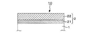
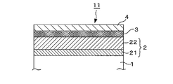
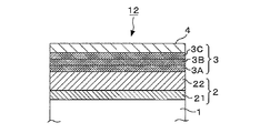
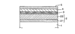
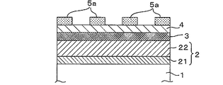
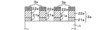
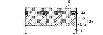
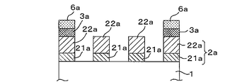
- FIG. 1 is a schematic cross-sectional view of an embodiment of a mask blank according to the present invention. It is the cross-sectional schematic of other embodiment of the mask blank which concerns on this invention. It is the cross-sectional schematic of other embodiment of the mask blank which concerns on this invention. It is a cross-sectional schematic diagram which shows one manufacturing process of the phase shift mask using the mask blank which concerns on this invention. It is a cross-sectional schematic diagram which shows one manufacturing process of the phase shift mask using the mask blank which concerns on this invention. It is a cross-sectional schematic diagram which shows one manufacturing process of the phase shift mask using the mask blank which concerns on this invention. It is a cross-sectional schematic diagram which shows one manufacturing process of the phase shift mask using the mask blank which concerns on this invention. It is a cross-sectional schematic diagram which shows one manufacturing process of the phase shift mask using the mask blank which concerns on this invention.
- the present invention is a mask blank for producing a phase shift mask to which laser exposure light having a wavelength of 200 nm or less is applied, as described in Configuration 1, and includes a phase shift film on a translucent substrate.
- the phase shift film includes a phase shift layer containing at least a transition metal and silicon, and a silicon layer that attenuates exposure light irradiated to the phase shift layer, and the silicon layer includes the phase shift layer.
- the present invention relates to a mask blank that is formed in contact with the substrate side of a shift layer.
- the mask blank of the present invention is particularly suitable for producing a halftone phase shift mask among the phase shift masks.
- FIG. 1 is a schematic sectional view showing an embodiment of a mask blank according to the present invention.
- an embodiment of a mask blank 10 according to the present invention has a structure in which a phase shift film 2 is provided on a translucent substrate 1.
- the phase shift film 2 includes a phase shift layer 22 containing at least a transition metal and silicon, and a silicon layer 21 that attenuates exposure light irradiated to the phase shift layer 22.
- the layer 21 is formed in contact with the substrate 1 side of the phase shift layer. That is, in the present embodiment, the phase soft film 2 in which the silicon layer 21 and the phase shift layer 22 are laminated in this order is provided on the translucent substrate 1.
- the translucent substrate 1 in the mask blank 10 is not particularly limited as long as it is a substrate used for a transfer mask for manufacturing a semiconductor device.
- a synthetic quartz substrate and other various glass substrates for example, soda lime glass, Aluminosilicate glass or the like.
- a synthetic quartz substrate is particularly preferably used because it is highly transparent in an ArF excimer laser (wavelength 193 nm) effective for fine pattern formation or in a shorter wavelength region.
- the phase shift film 2 has a laminated structure of a silicon layer 21 and a phase shift layer 22.
- the silicon layer 21 is present in the lower layer (substrate side) of the phase shift layer 22.
- the phase shift layer 22 is formed of a material containing at least a transition metal and silicon, but the configuration of the phase shift layer 22 applicable to the present invention is not particularly limited. For example, it has been conventionally used.
- the configuration of the phase shift film in the existing phase shift mask can be applied.
- phase shift layer 22 examples include, for example, a light semi-transmissive film containing a metal silicide composed of transition metal and silicon, or transition metal and silicon with optical properties and physical properties (etching rate, other films ( A light translucent film containing a transition metal silicide material containing one or more elements selected from oxygen, nitrogen or carbon in order to improve the etching selectivity with the layer) and the like is preferred.
- transition metal examples include molybdenum, tantalum, tungsten, titanium, chromium, nickel, vanadium, zirconium, ruthenium, and rhodium. Of these, molybdenum is particularly preferred. In the case where the transition metal is molybdenum, the problem of deterioration of the conventional phase shift film due to exposure light occurs remarkably, so that the effects of the present invention are particularly exhibited.
- the material containing at least a transition metal and silicon include a transition metal silicide or a transition metal silicide nitride, oxide, carbide, oxynitride, carbonate, or carbonitride. Is preferred.
- the phase shift layer 22 can be applied to either a single layer structure or a laminated structure including a low transmittance layer and a high transmittance layer.
- the preferable film thickness of the phase shift layer 22 varies depending on the material, but it is desirable that the phase shift layer 22 is appropriately adjusted particularly from the viewpoint of the phase shift function and light transmittance.
- the phase shift film 2 since the phase shift film 2 has a laminated structure of the silicon layer 21 and the phase shift layer 22, the phase shift film 2 as a whole is considered in consideration of the phase difference and the light transmittance of the silicon layer 21. From the viewpoint of the phase shift function and the light transmittance, it is desirable to adjust the film thickness of the phase shift layer 22.
- the silicon layer 21 located below the phase shift layer 22 has a function of attenuating the exposure light applied to the phase shift layer 22. Since the silicon layer 21 is present on the substrate side of the phase shift layer 22, that is, on the side irradiated with the exposure light, in the phase shift mask manufactured using this mask blank, the phase shift layer 22 has an attenuated exposure. Since light is irradiated, the transition metal contained in the phase shift layer 22 becomes difficult to be excited by the exposure light, and the oxidation and alteration of the phase shift layer 22 containing the transition metal silicide can be effectively suppressed. .
- substrate 1 for example, synthetic quartz glass
- silicon layer is allowed to contain an impurity element that inevitably enters in the thin film formation stage or an impurity element that enters due to a change with time after film formation.
- the impurity component contained in the target when a silicon layer is formed by sputtering, the impurity component contained in the target, the rare gas component that has entered the thin film during the film formation process, and other changes to the upper silicide film and the underlying substrate due to changes over time after film formation.
- the layer in which the derived component is slightly mixed is a concept included in the “silicon layer” in the present invention.
- the silicon compound layer containing other components in addition to silicon is not intentionally formed is included in the configuration of the present invention.
- the film density of the silicon layer 21 is preferably 2.1 g / cm 3 or more, and more preferably 2.2 g / cm 3 or more.
- voids increase in the Si layer, which may cause a component such as oxygen to be received from an adjacent substrate or an upper layer.
- the film density exceeds 2.5 g / cm 3 , there is a problem that the silicon layer 21 becomes too dense and the etching time when performing dry etching becomes too long. Therefore, a preferable film density is 2.1 g / cm 3 or more and 2.5 g / cm 3 or less, more preferably 2.2 g / cm 3 or more and 2.3 g / cm 3 or less.
- the film density can be measured by a known method such as an X-ray reflectance measurement method (XRR method) (the same applies hereinafter).
- the film thickness of the silicon layer 21 is not particularly limited, but in the present embodiment, it is preferable to be in the range of, for example, 3 nm or more and 20 nm or less. If the film thickness is less than 3 nm, the exposure light applied to the phase shift layer 22 is attenuated, and the effect of suppressing deterioration of the phase shift layer 22 may not be sufficiently exhibited. On the other hand, if the film thickness exceeds 20 nm, the attenuation amount of the exposure light energy applied to the phase shift layer 22 increases, which may affect the pattern transfer when manufacturing the semiconductor device.
- the optical characteristics of the entire phase shift film 2 need to be adjusted particularly from the viewpoint of the phase shift function and light transmittance.
- the silicon layer 21 of the present invention has a small refractive index, The influence on the phase difference in the phase shift layer 22 is relatively small. Therefore, it is desirable to design the phase shift film 2 (or the phase shift layer 22) mainly in consideration of the light transmittance of the silicon layer 21.
- the exposure light transmittance of the silicon layer 21 varies depending on the film thickness, it is preferably 30% or more and 70% or less, for example. Within this range, it becomes easy to adjust the exposure light transmittance of the upper phase shift layer 22.
- the phase shift film 2 is required to have a transmittance of 2% or more for exposure light.
- the transmittance with respect to the exposure light is required to be at least 2%.
- the transmittance of the phase shift film 2 with respect to exposure light is preferably 3% or more, and more preferably 4% or more.
- the transmittance of the phase shift film 2 for exposure light is preferably 30% or less, more preferably 20% or less, and even more preferably 10% or less.
- the phase shift film 2 has a phase difference of 150 between the transmitted ArF exposure light and the light that has passed through the air by the same distance as the thickness of the phase shift film 2. It is required to be adjusted to be in the range of not less than 180 degrees and not more than 180 degrees.
- the phase difference in the phase shift film 2 is preferably 155 degrees or more, and more preferably 160 degrees or more.
- the phase difference in the phase shift film 2 is preferably 179 degrees or less, and more preferably 177 degrees or less. This is to reduce the influence of an increase in phase difference caused by minute etching of the translucent substrate 1 during dry etching when forming a pattern on the phase shift film 2.
- the exposure light irradiation method to the phase shift mask by the exposure apparatus is increasing in which the exposure light is incident from a direction inclined at a predetermined angle with respect to the vertical direction of the film surface of the phase shift film 2. It is also for the purpose.
- the method for forming the phase shift film 2 composed of a laminated film in which the silicon layer 21 and the phase shift layer 22 are laminated in order on the light transmitting substrate 1 such as the mask blank 10 shown in FIG. 1 needs to be particularly restricted.
- the sputtering film forming method is preferable.
- the sputtering film forming method is preferable because a uniform film having a constant film thickness can be formed.
- the mask blank 10 of the present embodiment may have other constituent layers between the translucent substrate 1 and the phase shift film 2 as long as the effects of the present invention are not impaired.
- An example of such a constituent layer is an etching stopper layer made of a Cr-based material that is not etched by a fluorine-based gas.
- FIG. 2 is a schematic sectional view showing another embodiment of the mask blank according to the present invention.
- the mask blank according to the present invention has a phase shift film 2 made of a laminate of the silicon layer 21 and the phase shift layer 22 on the translucent substrate 1, and this phase shift film 2.
- a mask blank 11 having a structure in which a light shielding film 3 and a hard mask film 4 are further provided may be used. For example, it can be used for the production of a halftone phase shift mask having a light shielding band in the mask peripheral region. Since the phase shift film 2 including the translucent substrate 1, the silicon layer 21, and the phase shift layer 22 is already described, duplicate description is omitted here.
- the light shielding film 3 is provided for the purpose of transferring the pattern of the hard mask film 4 to the phase shift film 2 as faithfully as possible.
- the light shielding film 3 is formed of a material containing chromium in order to ensure etching selectivity with the phase shift layer 22 formed of a transition metal silicide-based material.
- the chromium-containing material include chromium (Cr) alone or a chromium compound in which elements such as oxygen, nitrogen, and carbon are added to chromium (for example, CrN, CrC, CrO, CrON, CrCN, CrOC, CrOCN, etc.). Can be mentioned.
- the material containing chromium forming the light shielding film 3 may contain one or more elements of molybdenum, indium and tin. By including one or more elements of molybdenum, indium and tin, the etching rate for the mixed gas of chlorine-based gas and oxygen gas can be further increased.
- the light-shielding film 3 may be formed of a material containing a transition metal and silicon as long as etching selectivity for dry etching can be obtained with the material forming the phase shift layer 22 (particularly the surface layer portion). . This is because a material containing a transition metal and silicon has a high light shielding performance, and the thickness of the light shielding film 3 can be reduced.
- transition metals to be contained in the light shielding film 3 molybdenum (Mo), tantalum (Ta), tungsten (W), titanium (Ti), chromium (Cr), hafnium (Hf), nickel (Ni), vanadium (V) , Zirconium (Zr), ruthenium (Ru), rhodium (Rh), zinc (Zn), niobium (Nb), palladium (Pd), and any one metal or an alloy of these metals.
- the metal element other than the transition metal element contained in the light shielding film 3 include aluminum (Al), indium (In), tin (Sn), and gallium (Ga).
- the light shielding film 3 may have a structure in which a layer made of a material containing chromium and a layer made of a material containing a transition metal and silicon are laminated in this order from the phase shift film 2 side.
- the specific matters of the material containing chromium and the material containing transition metal and silicon in this case are the same as those of the light shielding film 3 described above.
- the light shielding film 3 may have a single layer structure or a laminated structure. For example, a two-layer structure of a light-shielding layer and a front-surface antireflection layer, or a three-layer structure further including a back-surface antireflection layer can be used.
- FIG. 3 shows a mask blank 12 according to an embodiment in which the light shielding film 3 has a three-layer structure of a light shielding film lower layer 3A, a light shielding film intermediate layer 3B, and a light shielding film upper layer 3C.
- the film thickness of the light shielding film 3 is not particularly limited, it is usually preferably in the range of, for example, 30 nm or more and 80 nm or less from the viewpoint of securing a predetermined light shielding property.
- the light-shielding film 3 is required to have an optical density (OD) with respect to exposure light in the laminated structure of the phase shift film 2 of greater than 2.0, preferably 2.5 or more, and 2.8 or more. More preferably, it is more preferably 3.0 or more.
- the hard mask film 4 needs to be a material having high etching selectivity with the light shielding film 3 directly below, but in the present embodiment, a material containing silicon is particularly selected for the hard mask film 4.
- a material containing silicon is particularly selected for the hard mask film 4.
- the hard mask film 4 can be made of a material containing silicon (Si).
- a material containing silicon (Si) suitable for the hard mask film 4 is selected from silicon (Si), oxygen (O), nitrogen (N), carbon (C), boron (B), and hydrogen (H). Examples thereof include materials containing one or more elements.
- silicon (Si) and transition metals include oxygen (O), nitrogen (N), carbon (C), boron (B And a material containing one or more elements selected from hydrogen (H).
- transition metal examples include molybdenum (Mo), tungsten (W), titanium (Ti), tantalum (Ta), zirconium (Zr), hafnium (Hf), niobium (Nb), vanadium (V), Examples include cobalt (Co), chromium (Cr), nickel (Ni), ruthenium (Ru), and tin (Sn).
- the material constituting the hard mask film 4 include silicon oxide (SiO 2), silicon oxynitride (SiON), tantalum oxide (TaO), tantalum oxynitride (TaON), and tantalum boride oxide (TaBO). And tantalum boride oxynitride (TaBON). Since the hard mask film 4 formed of a material containing silicon and oxygen tends to have low adhesion to a resist film made of an organic material, the surface of the hard mask film 4 is subjected to HMDS (Hexamethyldisilazane) treatment. It is preferable to improve surface adhesion.
- HMDS Hexamethyldisilazane
- the film thickness of the hard mask film 4 need not be particularly limited, but it needs to be a film thickness that does not disappear at least before the etching of the light shielding film 3 immediately below is completed. On the other hand, if the hard mask film 4 is thick, it is difficult to reduce the thickness of the resist pattern immediately above. From such a viewpoint, it is preferable that it is the range of 2 nm or more and 20 nm or less, for example.
- the method for forming the light-shielding film 3 and the hard mask film 4 is not particularly limited, but among these, a sputtering film forming method is preferable.
- the sputtering film forming method is preferable because a uniform film having a constant film thickness can be formed.
- the thin film of SiN-based material has significantly higher ArF light resistance than the thin film of MoSi-based material.
- the pattern change CD (thickening) that occurs when the ArF excimer laser exposure light (hereinafter also referred to as ArF exposure light) is integrated after the transfer pattern is formed on the thin film of the SiN-based material is the conventional MoSi. This is greatly suppressed as compared with the case of a thin film of a system material. However, further extension of the life of the phase shift mask is desired.
- Si 3 N 4 is a stoichiometrically stable material, and the light resistance against ArF exposure light (hereinafter also referred to as ArF light resistance) is superior among materials composed of silicon and nitrogen.
- Si 3 N 4 has a higher refractive index n at the wavelength of ArF exposure light than SiNx having a low nitrogen content. Therefore, when Si 3 N 4 is applied as the material of the phase shift film, it is predetermined for ArF exposure light. It is possible to reduce the film thickness necessary for providing the above phase difference.
- the refractive index n when simply describing the refractive index n, it means the refractive index n with respect to the wavelength of the ArF exposure light, and when simply describing the extinction coefficient k, extinction with respect to the wavelength of the ArF exposure light. It means the coefficient k.
- the biggest cause of the CD change of the phase shift pattern which is a problem in ArF light resistance, is that when ArF exposure light is incident on the inside of the phase shift film, the elements constituting the phase shift film are photoexcited. It is considered.
- the transition metal molybdenum (Mo) is easily photoexcited, resulting in significant progress of oxidation of silicon (Si) from the surface, and the pattern volume greatly expands.
- the phase shift film of the MoSi-based material has a significant CD change (thickness) before and after irradiation with ArF exposure light.
- phase shift film made of a SiN-based material since the transition metal is not contained, the CD change before and after irradiation with ArF exposure light is relatively small. However, although silicon in the phase shift film is not as remarkable as the transition metal, it is photoexcited by irradiation with ArF exposure light.
- the phase shift film of the mask blank for manufacturing the phase shift mask is formed by sputtering under film forming conditions so as to have an amorphous or microcrystalline structure.
- Si 3 N 4 in a thin film of amorphous or microcrystalline structure is weakly bound state than Si 3 N 4 in the crystalline film. Therefore, the Si 3 N 4 phase shift film having an amorphous or microcrystalline structure is likely to be photoexcited by silicon in the film by irradiation with ArF exposure light. If the phase shift film is a crystal film of Si 3 N 4 , it is possible to suppress photoexcitation of silicon in the film.
- Si 3 N 4 is a material having a large refractive index n, but a significantly small extinction coefficient k at the wavelength of ArF exposure light. For this reason, when the phase shift film is formed of Si 3 N 4 and an attempt is made to design the predetermined phase difference to be slightly less than 180 degrees, only a high transmittance of about 20% or less can be produced. . If the nitrogen content of the SiN-based material is lowered, it is possible to produce a phase shift film having a predetermined phase difference and a predetermined transmittance. Naturally, however, the ArF light resistance also decreases as the nitrogen content decreases. Go.
- the mask blank 10 of the modified example preferably has the following configuration. That is, a mask blank 10 having a phase shift film 2 on a translucent substrate 1, the phase shift film 2 having a function of transmitting ArF excimer laser exposure light with a transmittance of 2% or more, and a phase shift A function of causing a phase difference of 150 degrees or more and 180 degrees or less between the exposure light transmitted through the film 2 and the exposure light transmitted through the air by the same distance as the thickness of the phase shift film 2;
- the phase shift film 2 includes a structure in which a silicon layer 21 and a phase shift layer 22 are laminated in this order from the translucent substrate 1 side.
- the phase shift layer 22 is made of a material composed of silicon and nitrogen, except for the surface layer portion thereof.
- the phase shift layer 22 is formed of a material containing one or more elements selected from non-metal elements and metalloid elements excluding oxygen in a material composed of silicon and nitrogen, and the phase shift layer 22 is thicker than the silicon layer 21. And it is characterized in and.
- the silicon layer 21 of the phase shift film 2 is disposed on the translucent substrate 1 side.
- the reflectance hereinafter also referred to as the back surface reflectance
- the light intensity of ArF exposure light incident on the inside of the silicon layer 21 is reduced, generation of silicon photoexcitation inside the silicon layer 21 and the phase shift layer 22 can be reduced. By acting on these, the ArF light resistance of the entire phase shift film 2 can be greatly enhanced.
- the silicon layer 21 has a higher function of attenuating ArF exposure light transmitted through the layer than the phase shift layer 22 made of SiN material. For this reason, even if the nitrogen content of the phase shift layer 22 is increased, the phase difference for the entire exposure light of the phase shift film 2 is within the above range, and the transmittance for the exposure light is 10% or less. Can do. Other matters (film density and the like) related to the silicon layer 21 in this modification are the same as those of the silicon layer 21 in the above embodiments.
- the phase shift layer 22 of this modification preferably has a film density higher than 2.5 g / cm 3, more preferably 2.6 g / cm 3 or more.
- the film density is less than 2.5 g / cm 3 , voids increase in the SiN film, so that a component such as oxygen may be accepted from the atmosphere or the like.
- the film density of the phase shift layer 22 exceeds 3.0 g / cm 3 , there is a problem that the Si—N bond in the film becomes too dense and the etching time when performing dry etching becomes too long.
- the film density of the phase shift layer 22 is a 3.0 g / cm 3 or less, more preferably 2.9 g / cm 3 or less.
- the thickness of the silicon layer 21 of this modification is as thin as possible within the range where the above-described conditions required for the phase shift film 2 can be satisfied.
- the thickness of the silicon layer 21 is preferably less than 12 nm, more preferably 11 nm or less, and even more preferably 10 nm or less.
- the thickness of the silicon layer 21 is preferably 3 nm or more, more preferably 4 nm or more, and further preferably 5 nm or more.
- the phase shift layer 22 of this modification is formed of a material having relatively high ArF light resistance, the phase shift layer 2 has a phase relative to the entire film thickness of the phase shift film 2 within a range that satisfies the above-described conditions required for the phase shift film 2. It is desirable to increase the thickness ratio of the shift layer 22 as much as possible.
- the thickness of the phase shift layer 22 is preferably not less than 5 times the thickness of the silicon layer 21, more preferably not less than 5.5 times, and further preferably not less than 6 times. Further, the thickness of the phase shift layer 22 is more preferably 10 times or less the thickness of the silicon layer 21.
- the thickness of the phase shift layer 22 is preferably 80 nm or less, more preferably 70 nm or less, and further preferably 65 nm or less. Further, the thickness of the phase shift layer 22 is preferably 50 nm or more, and more preferably 55 nm or more.
- the phase shift layer 22 of this modification contains at least one element selected from a non-metal element and a semi-metal element excluding oxygen in a material consisting of silicon and nitrogen, or a material consisting of silicon and nitrogen, except for the surface layer portion. It is made of a material that The surface layer portion of the phase shift layer 22 refers to the surface layer portion on the opposite side of the phase shift layer 22 from the silicon layer 21 side.
- the phase shift layer 22 is preferably a material having a high refractive index n. Since the refractive index n tends to decrease as the oxygen content in the material increases, oxygen is not actively contained in the phase shift layer 22 during film formation except for the surface layer portion (the oxygen content is , Below the lower limit of detection when composition analysis is performed by X-ray photoelectron spectroscopy or the like.) From these things, the surface layer part of the phase shift layer 22 is formed with the material which added oxygen to the material which forms the phase shift layer 22 except a surface layer part.
- the surface layer portion of the phase shift layer 22 of this modification may be formed by various oxidation treatments. This is because the surface layer can be a stable oxide layer.
- this oxidation treatment for example, heat treatment in a gas containing oxygen such as the atmosphere, light irradiation treatment with a flash lamp or the like in a gas containing oxygen, ozone or oxygen plasma is brought into contact with the surface of the phase shift layer 22. Processing.
- the surface layer portion of the phase shift layer 22 preferably has a thickness of 1 nm or more, and more preferably 1.5 nm or more. Further, the surface layer portion of the phase shift layer 22 preferably has a thickness of 5 nm or less, and more preferably 3 nm or less.
- the phase shift layer 22 of this modification does not contain a transition metal that can cause a decrease in light resistance to ArF exposure light. Since it is impossible to deny the possibility that the light resistance to ArF exposure light can be reduced, it is desirable not to include metal elements other than transition metals.
- the phase shift layer 22 may contain any metalloid element in addition to silicon and nitrogen. Among these metalloid elements, it is preferable to include one or more elements selected from boron, germanium, antimony, and tellurium because it can be expected to increase the conductivity of silicon used as a sputtering target.
- the phase shift layer 22 of this modification may contain a nonmetallic element other than oxygen in addition to silicon and nitrogen.
- these nonmetallic elements it is preferable to include one or more elements selected from carbon, fluorine and hydrogen.
- This nonmetallic element also includes rare gases such as helium (He), argon (Ar), krypton (Kr), and xenon (Xe).
- the phase shift layer 22 is preferably a material having a higher refractive index n, and the silicon-based material tends to have a higher refractive index n as the nitrogen content increases.
- the nitrogen content in the material forming the phase shift layer 22 is preferably greater than 50 atomic%, more preferably 52 atomic% or more, and even more preferably 55 atomic% or more.
- the matters relating to the translucent substrate 1, the light shielding film 3, and the hard mask film 4 are the same as those in the mask blank 10 of each of the above embodiments.
- the present invention also provides a phase shift mask manufactured from the mask blank according to the present invention and a method for manufacturing the same.
- 4A to 4E and FIG. 5A (continuation of FIG. 4E) to FIG. 5D are schematic cross-sectional views of a mask blank and the like showing a manufacturing process of a phase shift mask using the mask blank of the present invention.
- description will be made using the mask blank 11 of the embodiment shown in FIG.
- a resist film 5 for electron beam drawing is formed on the surface of the mask blank 11 by spin coating (see FIG. 4A).
- a predetermined pattern is drawn on the resist film 5 by electron beam, and after the drawing, development is performed to form a predetermined resist pattern 5a (see FIG. 4B).
- the resist pattern 5a has a desired device pattern to be formed on the phase shift film 2 to be a final transfer pattern.
- the hard mask film 4 corresponds to the pattern formed on the phase shift film 2 by dry etching using a fluorine-based gas.
- a hard mask film pattern 4a is formed (see FIG. 4C).
- the light-shielding film 3 and the phase shift film 2 are formed by dry etching using a mixed gas of chlorine gas and oxygen gas using the hard mask film pattern 4a as a mask.
- a light shielding film pattern 3a corresponding to the pattern is formed (see FIG. 4D).
- phase shift film 2 formed by stacking the silicon layer 21 and the phase shift layer 22 is continuously performed by dry etching using a fluorine-based gas using the light shielding film pattern 3a as a mask.
- a pattern 2a is formed (see FIG. 4E).
- the hard mask film pattern 4a exposed on the surface is removed.
- a resist film 6 similar to that described above is formed by spin coating on the entire surface of the substrate in the state shown in FIG. 4E (see FIG. 5A), and a predetermined device pattern (for example, A pattern corresponding to the light-shielding band pattern) is drawn and developed to form a predetermined resist pattern 6a (see FIG. 5B).
- a predetermined device pattern for example, A pattern corresponding to the light-shielding band pattern
- the exposed light shielding film pattern 3a is etched by dry etching using a mixed gas of chlorine gas and oxygen gas, for example, a light shielding film in a transfer pattern forming region.
- the pattern 3a is removed, and a light-shielding band pattern is formed around the transfer pattern formation region (see FIG. 5C).
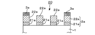
- a phase shift mask for example, a halftone phase shift mask 20 is completed (see FIG. 5D).
- the completed phase shift mask 20 is provided with a phase shift film pattern 2a on the translucent substrate 1, and the phase shift film pattern 2a includes the silicon layer pattern 21a and the phase shift film pattern 2a.
- the phase shift layer pattern 22a has a laminated structure, and the silicon layer pattern 21a is present in the lower layer (substrate side) of the phase shift layer pattern 22a.
- the phase shift layer 22 is irradiated with attenuated exposure light due to the presence of the silicon layer 21, so that the transition metal contained in the phase shift layer 22 is exposed to exposure light.
- the phase shift layer 22 containing transition metal silicide can be effectively suppressed from being oxidized and altered. According to the present invention, it is possible to obtain a phase shift mask having excellent light resistance of the transition metal silicide phase shift film with respect to exposure light having a wavelength of 200 nm or less and excellent quality stability.
- a method of manufacturing a semiconductor device including a step of pattern transfer of a transfer pattern of the phase shift mask onto a semiconductor substrate by lithography using a phase shift mask manufactured using such a mask blank of the present invention According to this, a high-quality semiconductor device having excellent pattern accuracy can be obtained.
- the phase shift mask manufactured from the mask blank of the above-described modification and the manufacturing method thereof are the same as those in the above-described manufacturing method of the phase shift mask and the phase shift mask according to the present invention.
- the phase shift layer 22 made of silicon and nitrogen such as SiN the light intensity of the exposure light incident on the silicon layer 21 is reduced, so that the inside of the silicon layer 21 and the phase shift layer 22
- the generation of photoexcitation of silicon in the substrate can be reduced, and oxidation and alteration of the phase shift layer 22 containing the SiN-based material can be effectively suppressed.
- the manufacturing method of the semiconductor device using the phase shift mask of the above modification is the same as that of the manufacturing method of the semiconductor device according to the present invention.
- the mask blank, the method for manufacturing a phase shift mask, and the method for manufacturing a semiconductor device of the above modification have the following configurations, for example.
- (Configuration 1A) A mask blank provided with a phase shift film on a translucent substrate, The phase shift film has a function of transmitting exposure light of ArF excimer laser with a transmittance of 2% or more, and in the air by the same distance as the thickness of the phase shift film with respect to the exposure light transmitted through the phase shift film.
- the phase shift film includes a structure in which a silicon layer and a phase shift layer are laminated in this order from the translucent substrate side,
- the phase shift layer is formed of a material containing one or more elements selected from a non-metal element and a metalloid element excluding oxygen in a material consisting of silicon and nitrogen or a material consisting of silicon and nitrogen except for the surface layer portion thereof,
- the mask blank wherein the phase shift layer is thicker than the silicon layer.
- Configuration 8A The mask blank according to any one of configurations 1A to 7A, further comprising: a light-shielding film made of a material containing chromium on a surface of the phase shift film opposite to the substrate.
- Configuration 9A The mask blank according to Configuration 8A, comprising a hard mask film made of a material containing silicon on a surface of the light shielding film opposite to the phase shift film.
- (Configuration 10A) A method of manufacturing a phase shift mask, comprising a step of patterning the phase shift film in the mask blank according to any one of configurations 1A to 9A.
- phase shift mask having a phase shift film pattern on a translucent substrate,
- the phase shift film pattern has a function of transmitting exposure light of ArF excimer laser with a transmittance of 2% or more, and the same distance as the thickness of the phase shift film with respect to the exposure light transmitted through the phase shift film pattern.
- the phase shift film pattern includes a structure in which a silicon layer and a phase shift layer are laminated in this order from the translucent substrate side,
- the phase shift layer is formed of a material containing one or more elements selected from a non-metal element and a metalloid element excluding oxygen in a material consisting of silicon and nitrogen or a material consisting of silicon and nitrogen except for the surface layer portion thereof,
- the phase shift mask is characterized in that the phase shift layer is thicker than the silicon layer.
- (Configuration 12A) The phase shift mask according to Configuration 11A, wherein a film density of the silicon layer is 2.1 g / cm 3 or more and 2.5 g / cm 3 or less.
- (Configuration 14A) 14 The phase shift mask according to any one of configurations 11 ⁇ / b> A to 13 ⁇ / b> A, wherein the thickness of the phase shift layer is five times or more the thickness of the silicon layer.
- (Configuration 15A) 14 The phase shift mask according to any one of configurations 11 ⁇ / b> A to 14 ⁇ / b> A, wherein a thickness of the silicon layer is 3 nm or more and less than 12 nm.
- (Configuration 16A) The phase shift mask according to any one of Structures 11A to 15A, wherein the thickness of the phase shift layer is 80 nm or less.
- (Configuration 17A) The phase shift mask according to any one of configurations 11A to 16A, wherein the phase shift layer has a nitrogen content greater than 50 atomic%.
- (Configuration 19A) A step of transferring a pattern of the phase shift mask onto a semiconductor substrate by a lithography method using the phase shift mask manufactured by the method of manufacturing a phase shift mask described in Structure 10A. Production method.
- (Configuration 20A) A method of manufacturing a semiconductor device, comprising: using the phase shift mask according to any one of Structures 11A to 18A and transferring a pattern of the phase shift mask onto a semiconductor substrate by lithography.
- the present embodiment relates to the manufacture of a mask blank and a phase shift mask used for manufacturing a halftone phase shift mask using an ArF excimer laser having a wavelength of 193 nm as exposure light.
- a mask blank 12 used in this example is a phase shift film 2 and a three-layer laminate composed of a laminate of a silicon layer 21 and a phase shift layer 22 on a translucent substrate (glass substrate) 1 as shown in FIG. In this structure, the light shielding film 3 and the hard mask film 4 having a structure are sequentially laminated.
- This mask blank 12 was produced as follows.
- a synthetic quartz substrate (size: about 152 mm ⁇ 152 mm ⁇ thickness 6.35 mm) was prepared as the glass substrate 1.
- the phase shift film 2 composed of a laminate of the silicon layer 21 and the phase shift layer 22 was formed.
- a silicon (Si) layer 21 was formed with a thickness of 8 nm.
- the formed Si layer 21 had a refractive index of 0.95 and an extinction coefficient of 2.70 for exposure light having a wavelength of 193 nm.
- the formed MoSiON layer 22 had a refractive index of 2.38 and an extinction coefficient of 0.32 with respect to exposure light having a wavelength of 193 nm.
- the phase shift film 2 having a two-layer structure formed as described above had a total film thickness of 83 nm, a phase difference of 176.3 degrees with respect to exposure light having a wavelength of 193 nm, and a transmittance of 6.08%.
- a light shielding film 3 having a laminated structure of a lower layer 3A made of a CrOCN film, an intermediate layer 3B made of a CrN film, and an upper layer 3A made of a CrOCN film was formed on the phase shift film 2.
- the light-shielding film lower layer 3A made of a CrOCN film having a thickness of 30 nm was formed on the phase shift film 2 by performing reactive sputtering.
- a hard mask film 4 made of a SiO 2 film was formed on the light shielding film 3. Specifically, SiO 2 having a thickness of 5 nm is formed on the light-shielding film 3 by performing reactive sputtering in an argon (Ar) gas atmosphere (pressure 0.3 Pa) using a silicon dioxide (SiO 2 ) target. A hard mask film 4 composed of two films was formed.
- the optical density of the laminated film of the phase shift film 2 and the light shielding film 3 was 3.0 or more (transmittance of 0.1% or less) at the wavelength (193 nm) of ArF excimer laser.
- the mask blank 12 of this example was produced as described above.
- a halftone phase shift mask was manufactured according to the manufacturing steps shown in FIGS. 4A to 4E and FIGS. 5A to 5D.
- the following symbols correspond to those in FIGS. 4A to 4E and FIGS. 5A to 5D.
- an HMDS process is performed on the upper surface of the mask blank 12, and a chemical amplification resist for electron beam drawing (PRL009 made by Fuji Film Electronics Materials) is applied by spin coating, and a predetermined baking process is performed.
- a resist film 5 having a thickness of 80 nm was formed (see FIG. 4A).
- a predetermined device pattern (pattern corresponding to the phase shift pattern to be formed on the phase shift film 2) is drawn on the resist film 5 using an electron beam drawing machine, and then the resist film is developed.
- a resist pattern 5a was formed (see FIG. 4B).
- the hard mask film 4 was dry etched to form a hard mask film pattern 4a (see FIG. 4C).
- a fluorine-based gas (CF 4 ) was used as the dry etching gas.
- the light shielding film 3 composed of the laminated film of the upper layer 3C, the intermediate layer 3B, and the lower layer 3A is continuously subjected to dry etching, and the light shielding film pattern 3a is formed. Formed (see FIG. 4D).
- phase shift film 2 formed by stacking the silicon layer 21 and the phase shift layer 22 is continuously dry-etched to form the phase shift film pattern 2a (see FIG. 4E).
- a fluorine-based gas (SF 6 ) was used as the dry etching gas.
- the hard mask film pattern 4a exposed on the surface was removed.
- a resist film 6 similar to that described above is formed by spin coating on the entire surface of the substrate in the state shown in FIG. 4E (see FIG. 5A), and a predetermined device pattern (for example, A pattern corresponding to the shading band pattern) was drawn and developed to form a predetermined resist pattern 6a (see FIG. 5B).
- a predetermined device pattern for example, A pattern corresponding to the shading band pattern
- the exposed light-shielding film pattern 3a is etched, for example, to remove the light-shielding film pattern 3a in the transfer pattern formation region, and in the periphery of the transfer pattern formation region.
- a shading band pattern was formed (see FIG. 5C).
- the obtained phase shift mask 20 was continuously irradiated with an ArF excimer laser so that the total irradiation amount was 30 kJ / cm 2 .
- the irradiation amount of 30 kJ / cm 2 corresponds to the use of the phase shift mask 20 approximately 100,000 times, and the frequency of use of the normal phase shift mask 20 This is equivalent to using for about 3 months.
- the transmittance and phase difference of the phase shift film 2 (Si layer + MoSiON layer) after irradiation were measured, the transmittance was 6.12% and the phase difference was 176.1 degrees in an ArF excimer laser (wavelength 193 nm). It was. Accordingly, the amount of change before and after irradiation is such that the transmittance is + 0.04% and the phase difference is ⁇ 0.2 degrees, and the amount of change is suppressed to a small level. There is no effect. Further, when the cross section of the phase shift film pattern 2a was observed in detail using a TEM (transmission electron microscope), a thick deteriorated layer, which has been generated in particular, was not confirmed, and the line width was increased (CD change amount).
- the mask blank of this example and the phase shift mask manufactured using the mask blank have extremely high light resistance against cumulative irradiation with an exposure light source having a short wavelength of 200 nm or less.
- Example 2 The mask blank of Example 2 was manufactured in the same procedure as the mask blank of Example 1 except that the SiN film was applied to the material for forming the phase shift layer 22 of the phase shift film 2. Specifically, the translucent substrate 1 is installed in a single-wafer RF sputtering apparatus, and a silicon (Si) target is used and RF sputtering using argon (Ar) gas as a sputtering gas is performed. A silicon layer 21 having a thickness of 8 nm was formed in contact with the surface.
- Si silicon
- Ar argon
- the phase shift film 2 in which the silicon layer 21 and the phase shift layer 22 were laminated in contact with the surface of the translucent substrate 1 was formed with a thickness of 71 nm.
- the thickness of the phase shift layer 22 is 7.9 times the thickness of the silicon layer 21.
- the composition of the phase shift layer 22 is a result obtained by measurement by X-ray photoelectron spectroscopy (XPS).
- the light-transmitting substrate 1 on which the phase shift film 2 was formed was subjected to heat treatment for reducing the film stress of the phase shift film 2 and forming an oxide layer on the surface layer portion.
- a phase shift measuring device MPM193, manufactured by Lasertec Corporation
- the transmittance and phase difference of the phase shift film 2 with respect to light having a wavelength of 193 nm were measured.
- the transmittance was 6.1% and the phase difference was 177.0. Degree.
- phase shift film 2 when this phase shift film 2 was analyzed by STEM (Scanning Electron Microscope) and EDX (Energy Dispersive X-Ray Spectroscopy), it was oxidized at the surface layer portion having a thickness of about 2 nm from the surface of the phase shift layer 22. It was confirmed that a layer was formed. Furthermore, when the optical characteristics of the silicon layer 21 and the phase shift layer 22 of the phase shift film 2 were measured, the silicon layer 21 had a refractive index n of 1.06 and an extinction coefficient k of 2.72. The layer 22 had a refractive index n of 2.63 and an extinction coefficient k of 0.37. The back surface reflectance (reflectance on the translucent substrate 1 side) of the phase shift film 2 with respect to light having a wavelength of 193 nm was 44.1%.
- a light shielding film 3 and a hard mask film 4 were formed on the phase shift film 2 in the same manner as the mask blank of Example 1.
- the mask of Example 2 having a structure in which the phase shift film 2 including the silicon layer 21 and the SiN phase shift layer 22, the light shielding film 3, and the hard mask film 4 are laminated on the translucent substrate 1 by the above procedure.
- a blank 12 was produced.
- the phase shift mask 20 of Example 2 was produced in the same procedure as in Example 1. Note that dry etching using SF 6 + He was performed on the phase shift film 2, and the ratio of the etching rate of the silicon layer 21 to the etching rate of the phase shift layer 22 at that time was 2.06.
- the ArF excimer laser light is irradiated and transferred to the resist film on the semiconductor device with the exposure light having a wavelength of 193 nm using the AIMS 193 (manufactured by Carl Zeiss) on the phase shift mask 20.
- the exposure transfer image was simulated at. When the exposure transfer image obtained by this simulation was verified, the design specifications were sufficiently satisfied. From the above, the phase shift mask 20 manufactured from the mask blank of Example 2 is set in an exposure apparatus and subjected to exposure transfer with exposure light of an ArF excimer laser until the integrated dose reaches 40 kJ / cm 2. In other words, it can be said that exposure transfer can be performed with high accuracy on the resist film on the semiconductor device.
- Example 2 In the mask blank used in Example 1, the light shielding film and the hard mask film were the same as Example 1 except that the formation of the silicon layer was omitted and the MoSiON layer was formed as a phase shift film on the surface of the substrate 1.
- the mask blank of the comparative example was produced.
- the light-transmitting substrate on which the MoSiON film was formed was subjected to heat treatment. Specifically, heat treatment was performed in the atmosphere at a heating temperature of 400 ° C. and a heating time of 2 hours.
- the MoSiON film had an transmittance of 6.11% and a phase difference of 175.6 degrees in an ArF excimer laser. Further, when the cross section of the MoSiON film after the heat treatment was observed in detail using a TEM (transmission electron microscope), there was no particular change in the surface layer portion of the MoSiON film, and no film was formed.
- Example 2 a phase shift mask was produced using the mask blank of the comparative example. Note that the transmittance and phase difference of the phase shift film in the produced phase shift mask were hardly changed from those at the time of manufacturing the mask blank.
- the obtained phase shift mask of this comparative example was continuously irradiated with an ArF excimer laser so that the total dose was 30 kJ / cm 2.
- the transmittance and phase difference of the phase shift film (MoSiON film) after irradiation were measured, the transmittance was 7.69% and the phase difference was 170.8 degrees in the ArF excimer laser. Therefore, the amount of change before and after irradiation is + 1.58% for the transmittance and the phase difference is ⁇ 4.8 degrees, and the amount of change is very large. When this amount of change occurs, it can be used as a photomask. I can't.
Landscapes
- Chemical & Material Sciences (AREA)
- Chemical Kinetics & Catalysis (AREA)
- Engineering & Computer Science (AREA)
- Materials Engineering (AREA)
- Mechanical Engineering (AREA)
- Metallurgy (AREA)
- Organic Chemistry (AREA)
- Physics & Mathematics (AREA)
- General Physics & Mathematics (AREA)
- Preparing Plates And Mask In Photomechanical Process (AREA)
Abstract
Description
また、上記特許文献2では、ケイ素と遷移金属の総和における遷移金属の遷移金属の割合が9原子%以下で、かつ、窒化が不十分な不完全窒化物膜を使用した光半透過膜の例が記載されている。この特許文献2では、遷移金属と窒素の結合、遷移金属とケイ素の結合をそれぞれ制御し、露光光照射に伴う遷移金属の酸化を防止し、耐光性を高めようとしている。
本発明者は、繰返し使用によって透過率や位相差変化が生じた位相シフトマスクの光半透過膜パターンを調べた結果、MoSi系膜の表層側にSiとO、若干のMoを含む変質層が出来ており、これが透過率や位相差の変化、線幅の変化(太り)の主な原因のひとつであることが判明した。そして、このような変質層が生じる理由(メカニズム)は次のように考えられる。すなわち、従来のスパッタ成膜されたMoSi系膜(光半透過膜)は構造的には隙間があり、成膜後にアニールしたとしてもMoSi膜の構造の変化が小さいため、フォトマスクの使用過程においてこの隙間にたとえば大気中の酸素(O2)や水(H2O)、酸素(O2)がArFエキシマレーザーと反応することによって発生するオゾン(O3)等が入り込んで、光半透過膜を構成するSiやMoと反応する。つまり、このような環境で光半透過膜を構成するSiとMoは露光光(特にArFなどの短波長光)の照射を受けると励起され遷移状態となり、Siが酸化及び膨張する(SiよりもSiO2の体積が大きいため)と共に、Moも酸化して光半透過膜の表層側に変質層が生成される。そしてフォトマスクの繰返し使用により、露光光の照射を累積して受けると、Siの酸化及び膨張がさらに進行すると共に、酸化されたMoは変質層中を拡散し、表面に析出して、例えばMoO3となって昇華し、その結果、変質層の厚みが次第に大きくなる(MoSi膜中での変質層の占める割合が大きくなる)ものと考えられる。このような変質層が発生し、さらに拡大していく現象は、光半透過膜を構成するSiやMoの酸化反応のきっかけとなるこれらの構成原子が励起され遷移状態となるのに必要なエネルギーを有するArFエキシマレーザー等の短波長の露光光の場合に顕著に確認される。
すなわち、上記課題を解決するため、本発明は以下の構成を有する。
波長200nm以下のレーザー露光光が適用される位相シフトマスクを作製するためのマスクブランクであって、透光性基板上に、位相シフト膜を備えており、前記位相シフト膜は、少なくとも遷移金属とケイ素を含有する位相シフト層と、該位相シフト層へ照射される露光光を減衰させるケイ素層とを有しており、前記ケイ素層は前記位相シフト層の前記基板側に接して形成されていることを特徴とするマスクブランク。
前記ケイ素層の膜密度は、2.1g/cm3以上2.5g/cm3以下であることを特徴とする構成1に記載のマスクブランク。
(構成3)
前記ケイ素層の膜厚は、3nm以上20nm以下であることを特徴とする構成1又は2に記載のマスクブランク。
前記ケイ素層の露光光透過率は、30%以上70%以下であることを特徴とする構成1乃至3のいずれかに記載のマスクブランク。
(構成5)
前記位相シフト層は、さらに窒素と酸素のいずれか一方または両方を含有することを特徴とする構成1乃至4のいずれかに記載のマスクブランク。
前記位相シフト層の遷移金属は、モリブデンであることを特徴とする構成1乃至5のいずれかに記載のマスクブランク。
(構成7)
前記位相シフト層の膜厚は、100nm以下であることを特徴とする構成1乃至6のいずれかに記載のマスクブランク。
前記位相シフト膜の前記基板とは反対側の表面に、クロムを主成分とする遮光膜を有することを特徴とする構成1乃至7のいずれかに記載のマスクブランク。
(構成9)
前記遮光膜の前記位相シフト膜とは反対側の表面に、ケイ素を含有するハードマスク膜を有することを特徴とする構成8に記載のマスクブランク。
構成1乃至9のいずれかに記載のマスクブランクにおける前記位相シフト膜をパターニングする工程を含むことを特徴とする位相シフトマスクの製造方法。
(構成11)
波長200nm以下のレーザー露光光が適用される位相シフトマスクであって、透光性基板上に、位相シフト膜パターンを備えており、前記位相シフト膜パターンは、少なくとも遷移金属とケイ素を含有する位相シフト層と、該位相シフト層へ照射される露光光を減衰させるケイ素層とを有しており、前記ケイ素層は前記位相シフト層の前記基板側に接して形成されていることを特徴とする位相シフトマスク。
構成10に記載の位相シフトマスクの製造方法により製造された位相シフトマスク、または構成11に記載の位相シフトマスクを用い、リソグラフィー法により前記位相シフトマスクの転写パターンを半導体基板上にパターン転写する工程を含むことを特徴とする半導体装置の製造方法。
また、この位相シフトマスクを用いたパターン転写により、パターン精度の優れた高品質の半導体装置を製造することができる。
前述のように、本発明者は、変質層の発生、拡大を抑える方策として、MoSi膜などの位相シフト膜へ照射される露光光を減衰させることに着目して鋭意検討した結果、以下の構成を有する本発明によって前記の課題を解決できることを見出したものである。
図1に示されるとおり、本発明に係るマスクブランク10の一実施の形態は、透光性基板1上に、位相シフト膜2を備えた構造を有する。ここで、上記位相シフト膜2は、少なくとも遷移金属とケイ素を含有する位相シフト層22と、該位相シフト層22へ照射される露光光を減衰させるケイ素層21とを有しており、上記ケイ素層21は上記位相シフト層の基板1側に接して形成されている。すなわち、本実施の形態では、透光性基板1上に、ケイ素層21、位相シフト層22がこの順に積層された位相ソフト膜2を有している。
上記位相シフト層22は、少なくとも遷移金属とケイ素を含有する材料で形成されるが、本発明に適用可能な上記位相シフト層22の構成は特に限定される必要はなく、例えば従来から使用されている位相シフト型マスクにおける位相シフト膜の構成を適用することができる。
上記位相シフト層22の好ましい膜厚は、材質によっても異なるが、特に位相シフト機能、光透過率の観点から適宜調整されることが望ましい。また、本発明においては、上記位相シフト膜2が、ケイ素層21と位相シフト層22の積層構造からなるため、ケイ素層21の位相差、光透過率も考慮して、位相シフト膜2全体の位相シフト機能、光透過率の観点からも、上記位相シフト層22の膜厚を調整することが望ましい。通常は、たとえば100nm以下、さらに好ましくは80nm以下の範囲であることが好適である。
上記ケイ素層21が位相シフト層22の基板側、つまり露光光が照射される側に存在することにより、このマスクブランクを用いて作製された位相シフトマスクにおいて、位相シフト層22には減衰した露光光が照射されることになるため、位相シフト層22に含まれる遷移金属が露光光によって励起され難くなり、遷移金属シリサイドを含む位相シフト層22の酸化、変質を効果的に抑制することができる。したがって、波長200nm以下の露光光に対する遷移金属シリサイド系位相シフト膜の耐光性に優れ、かつ品質安定性に優れたマスクブランクを得ることができる。
また、ケイ素層であることにより透光性基板1(例えば合成石英ガラス)とのドライエッチング選択性も確保される。
上記ケイ素層21の露光光透過率は、膜厚によっても異なるが、例えば30%以上70%以下であることが好ましい。この範囲であると、上層の位相シフト層22の露光光透過率を調整しやすくなる。
本発明に係るマスクブランクは、図2に示されるように、透光性基板1上に、上記ケイ素層21と位相シフト層22の積層からなる位相シフト膜2を有し、この位相シフト膜2の上に、さらに遮光膜3とハードマスク膜4を設けた構成のマスクブランク11としてもよい。たとえば、マスク周辺領域に遮光帯を備えたハーフトーン型位相シフトマスクの作製に使用することができる。
上記透光性基板1、ケイ素層21と位相シフト層22の積層からなる位相シフト膜2についてはすでに説明したとおりであるので、ここでは重複した説明は省略する。
上記遮光膜3は、遷移金属シリサイド系材料で形成されている位相シフト層22とのエッチング選択性を確保するため、クロムを含有する材料で形成される。
上記クロムを含有する材料としては、例えばクロム(Cr)単体、あるいはクロムに酸素、窒素、炭素などの元素を添加したクロム化合物(例えばCrN,CrC,CrO,CrON,CrCN,CrOC,CrOCNなど)が挙げられる。
上記遮光膜3の膜厚は特に制約される必要はないが、所定の遮光性を確保する観点から、通常、例えば30nm以上80nm以下の範囲であることが好ましい。なお、遮光膜3は、位相シフト膜2の積層構造での露光光に対する光学濃度(OD)が2.0よりも大きいことが求められ、2.5以上であると好ましく、2.8以上であるとより好ましく、3.0以上であるとさらに好ましい。
なお、ケイ素と酸素を含有する材料で形成されたハードマスク膜4は、有機系材料のレジスト膜との密着性が低い傾向があるため、ハードマスク膜4の表面をHMDS(Hexamethyldisilazane)処理を施し、表面の密着性を向上させることが好ましい。
また、図1~図3には図示していないが、マスクブランクの表面にレジスト膜を有する形態のものも本発明のマスクブランクに含まれる。
図4A~図4E及び図5A(図4Eの続き)~図5Dは、本発明のマスクブランクを用いた位相シフトマスクの製造工程を示すマスクブランク等の断面概略図である。なお、ここでは前述の図2に示す実施形態のマスクブランク11を用いて説明する。
次に、このレジスト膜5に対して、所定のパターンを電子線描画し、描画後、現像することにより、所定のレジストパターン5aを形成する(図4B参照)。このレジストパターン5aは最終的な転写パターンとなる位相シフト膜2に形成されるべき所望のデバイスパターンを有する。
最後に、残存するレジストパターン6aを除去することにより、位相シフトマスク(たとえばハーフトーン型位相シフトマスク)20が出来上がる(図5D参照)。
(構成1A)
透光性基板上に位相シフト膜を備えたマスクブランクであって、
前記位相シフト膜は、ArFエキシマレーザーの露光光を2%以上の透過率で透過させる機能と、前記位相シフト膜を透過した前記露光光に対して前記位相シフト膜の厚さと同じ距離だけ空気中を通過した露光光との間で150度以上180度以下の位相差を生じさせる機能とを有し、
前記位相シフト膜は、透光性基板側からケイ素層と位相シフト層がこの順に積層した構造を含み、
前記位相シフト層は、その表層部分を除きケイ素および窒素からなる材料またはケイ素および窒素からなる材料に酸素を除く非金属元素および半金属元素から選ばれる1以上の元素を含有する材料で形成され、
前記位相シフト層は、前記ケイ素層よりも厚さが厚いことを特徴とするマスクブランク。
前記ケイ素層の膜密度は、2.1g/cm3以上2.5g/cm3以下であることを特徴とする構成1Aに記載のマスクブランク。
(構成3A)
前記位相シフト層の膜密度は、2.5g/cm3よりも大きく3.0g/cm3以下であることを特徴とする構成1A又は2Aに記載のマスクブランク。
前記位相シフト層の厚さは、前記ケイ素層の厚さの5倍以上であることを特徴とする構成1A乃至3Aのいずれかに記載のマスクブランク。
(構成5A)
前記ケイ素層の厚さは、3nm以上12nm未満であることを特徴とする構成1A乃至4Aのいずれかに記載のマスクブランク。
前記位相シフト層の膜厚は、80nm以下であることを特徴とする構成1A乃至5Aのいずれかに記載のマスクブランク。
(構成7A)
前記位相シフト層は、窒素含有量が50原子%よりも大きいことを特徴とする構成1A乃至6Aのいずれかに記載のマスクブランク。
前記位相シフト膜の前記基板とは反対側の表面に、クロムを含有する材料からなる遮光膜を有することを特徴とする構成1A乃至7Aのいずれかに記載のマスクブランク。
(構成9A)
前記遮光膜の前記位相シフト膜とは反対側の表面に、ケイ素を含有する材料からなるハードマスク膜を有することを特徴とする構成8Aに記載のマスクブランク。
構成1A乃至9Aのいずれかに記載のマスクブランクにおける前記位相シフト膜をパターニングする工程を含むことを特徴とする位相シフトマスクの製造方法。
透光性基板上に位相シフト膜パターンを備えた位相シフトマスクであって、
前記位相シフト膜パターンは、ArFエキシマレーザーの露光光を2%以上の透過率で透過させる機能と、前記位相シフト膜パターンを透過した前記露光光に対して前記位相シフト膜の厚さと同じ距離だけ空気中を通過した露光光との間で150度以上180度以下の位相差を生じさせる機能とを有し、
前記位相シフト膜パターンは、透光性基板側からケイ素層と位相シフト層がこの順に積層した構造を含み、
前記位相シフト層は、その表層部分を除きケイ素および窒素からなる材料またはケイ素および窒素からなる材料に酸素を除く非金属元素および半金属元素から選ばれる1以上の元素を含有する材料で形成され、
前記位相シフト層は、前記ケイ素層よりも厚さが厚いことを特徴とする位相シフトマスク。
前記ケイ素層の膜密度は、2.1g/cm3以上2.5g/cm3以下であることを特徴とする構成11Aに記載の位相シフトマスク。
(構成13A)
前記位相シフト層の膜密度は、2.5g/cm3よりも大きく3.0g/cm3以下であることを特徴とする構成11A又は12Aに記載の位相シフトマスク。
前記位相シフト層の厚さは、前記ケイ素層の厚さの5倍以上であることを特徴とする構成11A乃至13Aのいずれかに記載の位相シフトマスク。
(構成15A)
前記ケイ素層の厚さは、3nm以上12nm未満であることを特徴とする構成11A乃至14Aのいずれかに記載の位相シフトマスク。
前記位相シフト層の膜厚は、80nm以下であることを特徴とする構成11A乃至15Aのいずれかに記載の位相シフトマスク。
(構成17A)
前記位相シフト層は、窒素含有量が50原子%よりも大きいことを特徴とする構成11A乃至16Aのいずれかに記載の位相シフトマスク。
前記位相シフト膜パターンの前記基板とは反対側の表面に、クロムを含有する材料からなる遮光膜パターンを有することを特徴とする構成11A乃至17Aのいずれかに記載の位相シフトマスク。
構成10Aに記載の位相シフトマスクの製造方法により製造された位相シフトマスクを用い、リソグラフィー法により前記位相シフトマスクの転写パターンを半導体基板上にパターン転写する工程を含むことを特徴とする半導体装置の製造方法。
(構成20A)
構成11A乃至18Aのいずれかに記載の位相シフトマスクを用い、リソグラフィー法により前記位相シフトマスクの転写パターンを半導体基板上にパターン転写する工程を含むことを特徴とする半導体装置の製造方法。
(実施例1)
本実施例は、波長193nmのArFエキシマレーザーを露光光として用いるハーフトーン型位相シフトマスクの製造に使用するマスクブランク及び位相シフトマスクの製造に関する。
本実施例に使用するマスクブランク12は、図3に示すような、透光性基板(ガラス基板)1上に、ケイ素層21と位相シフト層22の積層からなる位相シフト膜2、3層積層構造の遮光膜3、ハードマスク膜4を順に積層した構造のものである。このマスクブランク12は、以下のようにして作製した。
次に、ケイ素層21と位相シフト層22の積層からなる位相シフト膜2を形成した。
まず、枚葉式RFスパッタリング装置内に上記合成石英基板1を設置し、シリコン(Si)ターゲットを用い、アルゴン(Ar)ガス(圧力=5×10⁻²Pa)をスパッタリングガスとし、RFスパッタリングにより、合成石英基板上に、ケイ素(Si)層21を8nmの厚さで形成した。形成したSi層21の屈折率は0.95、波長193nmの露光光に対する消衰係数は2.70であった。
以上のようにして形成した2層構造の位相シフト膜2は、総膜厚が83nm、波長193nmの露光光に対する位相差が176.3度、透過率が6.08%であった。
以上のようにして本実施例のマスクブランク12を作製した。
まず、上記マスクブランク12の上面にHMDS処理を行い、スピン塗布法によって、電子線描画用の化学増幅型レジスト(富士フィルムエレクトロニクスマテリアルズ社製 PRL009)を塗布し、所定のベーク処理を行って、膜厚80nmのレジスト膜5を形成した(図4A参照)。
上記レジストパターン5aを除去した後、上記ハードマスク膜パターン4aをマスクとして、上層3C、中間層3B及び下層3Aの積層膜からなる遮光膜3のドライエッチングを連続して行い、遮光膜パターン3aを形成した(図4D参照)。ドライエッチングガスとしてはCl2とO2の混合ガス(Cl2:O2=4:1(流量比))を用いた。
最後に、残存するレジストパターン6aを除去し、ハーフトーン型位相シフトマスク20を作製した(図5D参照)。
なお、上記位相シフト膜パターン2aの透過率、位相差はマスクブランク製造時と殆ど変化はなかった。
得られた位相シフトマスク20に対してマスク検査装置によってマスクパターンの検査を行った結果、設計値から許容範囲内で微細パターンが形成されていることが確認された。また、得られた位相シフトマスク20に対して、ArFエキシマレーザーを総照射量30kJ/cm2となるように連続照射した。前述したように、照射量30kJ/cm2(エネルギー密度 約25mJ/cm2)というのは、位相シフトマスク20を略100,000回使用したことに相当し、通常の位相シフトマスク20の使用頻度で略3カ月使用したことに相当する。
この実施例2のマスクブランクは、位相シフト膜2の位相シフト層22を形成する材料にSiN膜を適用したこと以外については、実施例1のマスクブランクと同様の手順で製造した。具体的には、枚葉式RFスパッタ装置内に透光性基板1を設置し、ケイ素(Si)ターゲットを用い、アルゴン(Ar)ガスをスパッタリングガスとするRFスパッタリングにより、透光性基板1の表面に接してケイ素層21を8nmの厚さで形成した。続いて、ケイ素(Si)ターゲットを用い、アルゴン(Ar)および窒素(N2)の混合ガスをスパッタリングガスとする反応性スパッタリング(RFスパッタリング)により、ケイ素層21上に、ケイ素および窒素からなる位相シフト層22(SiN膜 Si:N=43原子%:57原子%)を63nmの厚さで形成した。以上の手順により、透光性基板1の表面に接してケイ素層21と位相シフト層22が積層した位相シフト膜2を71nmの厚さで形成した。この位相シフト膜2は、位相シフト層22の厚さがケイ素層21の厚さの7.9倍ある。なお、位相シフト層22の組成は、X線光電子分光法(XPS)による測定によって得られた結果である。
得られた実施例2の位相シフトマスク20に対してマスク検査装置によってマスクパターンの検査を行った結果、設計値から許容範囲内で微細パターンが形成されていることが確認された。また、得られた位相シフトマスクに対して、ArFエキシマレーザーを総照射量40kJ/cm2となるように間欠照射する照射処理を行った。この照射処理前後における位相シフトパターン2aのCD変化量は1.5nmであった。
上記実施例1に使用したマスクブランクにおいて、ケイ素層の形成を省き、基板1の表面に、MoSiON層を位相シフト膜として形成したこと以外は、実施例1と同様にして遮光膜及びハードマスク膜を形成し、比較例のマスクブランクを作製した。
なお、上記MoSiON膜が形成された透光性基板に対して加熱処理を施した。具体的には、大気中で加熱温度を400℃、加熱時間を2時間の加熱処理を行った。なお、このMoSiON膜は、ArFエキシマレーザーにおいて、透過率は6.11%、位相差は175.6度となっていた。また、TEM(透過型電子顕微鏡)を用いて加熱処理後のMoSiON膜の断面を詳しく観察したところ、MoSiON膜の表層部分に特に変化はなく、被膜のようなものは形成されていなかった。
本出願は、2015年3月27日に出願された、日本国特許出願第2015-067259号からの優先権を基礎として、その利益を主張するものであり、その開示はここに全体として参考文献として取り込む。
2 位相シフト膜
21 ケイ素層
22 位相シフト層
3 遮光膜
4 ハードマスク膜
5,6 レジスト膜
10,11,12 マスクブランク
20 位相シフトマスク
Claims (33)
- 波長200nm以下のレーザー露光光が適用される位相シフトマスクを作製するためのマスクブランクであって、
透光性基板上に、位相シフト膜を備えており、
前記位相シフト膜は、少なくとも遷移金属とケイ素を含有する位相シフト層と、該位相シフト層へ照射される露光光を減衰させるケイ素層とを有しており、前記ケイ素層は前記位相シフト層の前記基板側に接して形成されていることを特徴とするマスクブランク。 - 前記ケイ素層の膜密度は、2.1g/cm3以上2.5g/cm3以下であることを特徴とする請求項1に記載のマスクブランク。
- 前記ケイ素層の膜厚は、3nm以上20nm以下であることを特徴とする請求項1又は2に記載のマスクブランク。
- 前記ケイ素層の露光光透過率は、30%以上70%以下であることを特徴とする請求項1乃至3のいずれかに記載のマスクブランク。
- 前記位相シフト層は、さらに窒素と酸素のいずれか一方または両方を含有することを特徴とする請求項1乃至4のいずれかに記載のマスクブランク。
- 前記位相シフト層の遷移金属は、モリブデンであることを特徴とする請求項1乃至5のいずれかに記載のマスクブランク。
- 前記位相シフト層の膜厚は、100nm以下であることを特徴とする請求項1乃至6のいずれかに記載のマスクブランク。
- 前記位相シフト膜の前記基板とは反対側の表面に、クロムを主成分とする遮光膜を有することを特徴とする請求項1乃至7のいずれかに記載のマスクブランク。
- 前記遮光膜の前記位相シフト膜とは反対側の表面に、ケイ素を含有するハードマスク膜を有することを特徴とする請求項8に記載のマスクブランク。
- 請求項1乃至9のいずれかに記載のマスクブランクにおける前記位相シフト膜をパターニングする工程を含むことを特徴とする位相シフトマスクの製造方法。
- 波長200nm以下のレーザー露光光が適用される位相シフトマスクであって、
透光性基板上に、位相シフト膜パターンを備えており、
前記位相シフト膜パターンは、少なくとも遷移金属とケイ素を含有する位相シフト層と、該位相シフト層へ照射される露光光を減衰させるケイ素層とを有しており、前記ケイ素層は前記位相シフト層の前記基板側に接して形成されていることを特徴とする位相シフトマスク。 - 透光性基板上に位相シフト膜を備えたマスクブランクであって、
前記位相シフト膜は、ArFエキシマレーザーの露光光を2%以上の透過率で透過させる機能と、前記位相シフト膜を透過した前記露光光に対して前記位相シフト膜の厚さと同じ距離だけ空気中を通過した露光光との間で150度以上180度以下の位相差を生じさせる機能とを有し、
前記位相シフト膜は、透光性基板側からケイ素層と位相シフト層がこの順に積層した構造を含み、
前記位相シフト層は、その表層部分を除きケイ素および窒素からなる材料またはケイ素および窒素からなる材料に酸素を除く非金属元素および半金属元素から選ばれる1以上の元素を含有する材料で形成され、
前記位相シフト層は、前記ケイ素層よりも厚さが厚いことを特徴とするマスクブランク。 - 前記ケイ素層の膜密度は、2.1g/cm3以上2.5g/cm3以下であることを特徴とする請求項12に記載のマスクブランク。
- 前記位相シフト層の膜密度は、2.5g/cm3よりも大きく3.0g/cm3以下であることを特徴とする請求項12又は13に記載のマスクブランク。
- 前記位相シフト層の厚さは、前記ケイ素層の厚さの5倍以上であることを特徴とする請求項12乃至14のいずれかに記載のマスクブランク。
- 前記ケイ素層の厚さは、3nm以上12nm未満であることを特徴とする請求項12乃至15のいずれかに記載のマスクブランク。
- 前記位相シフト層の膜厚は、80nm以下であることを特徴とする請求項12乃至16のいずれかに記載のマスクブランク。
- 前記位相シフト層は、窒素含有量が50原子%よりも大きいことを特徴とする請求項12乃至17のいずれかに記載のマスクブランク。
- 前記位相シフト膜の前記基板とは反対側の表面に、クロムを含有する材料からなる遮光膜を有することを特徴とする請求項12乃至18のいずれかに記載のマスクブランク。
- 前記遮光膜の前記位相シフト膜とは反対側の表面に、ケイ素を含有する材料からなるハードマスク膜を有することを特徴とする請求項19に記載のマスクブランク。
- 請求項12乃至20のいずれかに記載のマスクブランクにおける前記位相シフト膜をパターニングする工程を含むことを特徴とする位相シフトマスクの製造方法。
- 透光性基板上に位相シフト膜パターンを備えた位相シフトマスクであって、
前記位相シフト膜パターンは、ArFエキシマレーザーの露光光を2%以上の透過率で透過させる機能と、前記位相シフト膜パターンを透過した前記露光光に対して前記位相シフト膜の厚さと同じ距離だけ空気中を通過した露光光との間で150度以上180度以下の位相差を生じさせる機能とを有し、
前記位相シフト膜パターンは、透光性基板側からケイ素層と位相シフト層がこの順に積層した構造を含み、
前記位相シフト層は、その表層部分を除きケイ素および窒素からなる材料またはケイ素および窒素からなる材料に酸素を除く非金属元素および半金属元素から選ばれる1以上の元素を含有する材料で形成され、
前記位相シフト層は、前記ケイ素層よりも厚さが厚いことを特徴とする位相シフトマスク。 - 前記ケイ素層の膜密度は、2.1g/cm3以上2.5g/cm3以下であることを特徴とする請求項22に記載の位相シフトマスク。
- 前記位相シフト層の膜密度は、2.5g/cm3よりも大きく3.0g/cm3以下であることを特徴とする請求項22又は23に記載の位相シフトマスク。
- 前記位相シフト層の厚さは、前記ケイ素層の厚さの5倍以上であることを特徴とする請求項22乃至24のいずれかに記載の位相シフトマスク。
- 前記ケイ素層の厚さは、3nm以上12nm未満であることを特徴とする請求項22乃至25のいずれかに記載の位相シフトマスク。
- 前記位相シフト層の膜厚は、80nm以下であることを特徴とする請求項22乃至26のいずれかに記載の位相シフトマスク。
- 前記位相シフト層は、窒素含有量が50原子%よりも大きいことを特徴とする請求項22乃至27のいずれかに記載の位相シフトマスク。
- 前記位相シフト膜パターンの前記基板とは反対側の表面に、クロムを含有する材料からなる遮光膜パターンを有することを特徴とする請求項22乃至28のいずれかに記載の位相シフトマスク。
- 請求項10に記載の位相シフトマスクの製造方法により製造された位相シフトマスクを用い、リソグラフィー法により前記位相シフトマスクの転写パターンを半導体基板上にパターン転写する工程を含むことを特徴とする半導体装置の製造方法。
- 請求項11に記載の位相シフトマスクを用い、リソグラフィー法により前記位相シフトマスクの転写パターンを半導体基板上にパターン転写する工程を含むことを特徴とする半導体装置の製造方法。
- 請求項21に記載の位相シフトマスクの製造方法により製造された位相シフトマスクを用い、リソグラフィー法により前記位相シフトマスクの転写パターンを半導体基板上にパターン転写する工程を含むことを特徴とする半導体装置の製造方法。
- 請求項22乃至29のいずれかに記載の位相シフトマスクを用い、リソグラフィー法により前記位相シフトマスクの転写パターンを半導体基板上にパターン転写する工程を含むことを特徴とする半導体装置の製造方法。
Priority Applications (2)
| Application Number | Priority Date | Filing Date | Title |
|---|---|---|---|
| KR1020177030296A KR102069960B1 (ko) | 2015-03-27 | 2016-03-24 | 마스크 블랭크, 위상 시프트 마스크 및 위상 시프트 마스크의 제조 방법, 및 반도체 장치의 제조 방법 |
| US15/561,124 US10365556B2 (en) | 2015-03-27 | 2016-03-24 | Mask blank, phase shift mask, method for manufacturing phase shift mask, and method for manufacturing semiconductor device |
Applications Claiming Priority (2)
| Application Number | Priority Date | Filing Date | Title |
|---|---|---|---|
| JP2015-067259 | 2015-03-27 | ||
| JP2015067259 | 2015-03-27 |
Publications (1)
| Publication Number | Publication Date |
|---|---|
| WO2016158649A1 true WO2016158649A1 (ja) | 2016-10-06 |
Family
ID=57006798
Family Applications (1)
| Application Number | Title | Priority Date | Filing Date |
|---|---|---|---|
| PCT/JP2016/059326 Ceased WO2016158649A1 (ja) | 2015-03-27 | 2016-03-24 | マスクブランク、位相シフトマスク及び位相シフトマスクの製造方法、並びに半導体装置の製造方法 |
Country Status (5)
| Country | Link |
|---|---|
| US (1) | US10365556B2 (ja) |
| JP (2) | JP6073028B2 (ja) |
| KR (1) | KR102069960B1 (ja) |
| TW (1) | TWI682233B (ja) |
| WO (1) | WO2016158649A1 (ja) |
Cited By (6)
| Publication number | Priority date | Publication date | Assignee | Title |
|---|---|---|---|---|
| JP2018077418A (ja) * | 2016-11-11 | 2018-05-17 | Hoya株式会社 | マスクブランク、転写用マスク、転写用マスクの製造方法および半導体デバイスの製造方法 |
| CN108957941A (zh) * | 2017-05-18 | 2018-12-07 | 思而施技术株式会社 | 相移空白掩膜及其制造方法 |
| CN109782525A (zh) * | 2017-11-14 | 2019-05-21 | 爱发科成膜株式会社 | 掩模基底及其制造方法、相移掩模及其制造方法 |
| WO2019163310A1 (ja) * | 2018-02-22 | 2019-08-29 | Hoya株式会社 | マスクブランク、位相シフトマスク及び半導体デバイスの製造方法 |
| CN115933308A (zh) * | 2017-03-16 | 2023-04-07 | Hoya株式会社 | 掩模坯料、转印用掩模及半导体器件的制造方法 |
| JP2023154019A (ja) * | 2017-05-22 | 2023-10-18 | エヌチェーン ライセンシング アーゲー | パラメータ化可能なスマートコントラクト |
Families Citing this family (9)
| Publication number | Priority date | Publication date | Assignee | Title |
|---|---|---|---|---|
| JP6058757B1 (ja) * | 2015-07-15 | 2017-01-11 | Hoya株式会社 | マスクブランク、位相シフトマスク、位相シフトマスクの製造方法および半導体デバイスの製造方法 |
| KR102366782B1 (ko) * | 2016-07-25 | 2022-02-23 | 호야 가부시키가이샤 | 마스크 블랭크, 전사용 마스크, 전사용 마스크의 제조 방법 및 반도체 디바이스의 제조 방법 |
| JP6740107B2 (ja) * | 2016-11-30 | 2020-08-12 | Hoya株式会社 | マスクブランク、転写用マスク及び半導体デバイスの製造方法 |
| JP6812236B2 (ja) * | 2016-12-27 | 2021-01-13 | Hoya株式会社 | 位相シフトマスクブランク及びこれを用いた位相シフトマスクの製造方法、並びに表示装置の製造方法 |
| JP7126836B2 (ja) * | 2017-03-28 | 2022-08-29 | Hoya株式会社 | 位相シフトマスクブランク及びそれを用いた位相シフトマスクの製造方法、並びにパターン転写方法 |
| TWI847949B (zh) * | 2018-11-30 | 2024-07-01 | 日商Hoya股份有限公司 | 光罩基底、光罩之製造方法及顯示裝置之製造方法 |
| JP7350682B2 (ja) * | 2020-03-23 | 2023-09-26 | Hoya株式会社 | マスクブランク及び転写用マスクの製造方法 |
| JP7296927B2 (ja) * | 2020-09-17 | 2023-06-23 | 信越化学工業株式会社 | 位相シフトマスクブランク、位相シフトマスクの製造方法、及び位相シフトマスク |
| DE102023112057A1 (de) * | 2022-08-31 | 2024-02-29 | Taiwan Semiconductor Manufacturing Co., Ltd. | Verfahren zum herstellen von fotomasken |
Citations (6)
| Publication number | Priority date | Publication date | Assignee | Title |
|---|---|---|---|---|
| JPH0683034A (ja) * | 1992-07-17 | 1994-03-25 | Toshiba Corp | 露光用マスク、露光マスク用基板及びその製造方法 |
| JPH07128840A (ja) * | 1993-11-02 | 1995-05-19 | Hoya Corp | ハーフトーン型位相シフトマスク及びハーフトーン型位相シフトマスクブランク |
| JP2002258460A (ja) * | 2000-12-26 | 2002-09-11 | Hoya Corp | ハーフトーン型位相シフトマスクブランク及びマスク |
| JP2004004791A (ja) * | 2002-04-25 | 2004-01-08 | Hoya Corp | ハーフトーン型位相シフトマスクブランク及びハーフトーン型位相シフトマスク |
| JP2005208282A (ja) * | 2004-01-22 | 2005-08-04 | Hoya Corp | ハーフトーン型位相シフトマスクブランクの製造方法、及びハーフトーン型位相シフトマスクの製造方法 |
| JP2006209128A (ja) * | 2005-01-27 | 2006-08-10 | Applied Materials Inc | 保護マスクを使用したホトマスクプラズマエッチング方法 |
Family Cites Families (16)
| Publication number | Priority date | Publication date | Assignee | Title |
|---|---|---|---|---|
| JP3410089B2 (ja) * | 1991-11-13 | 2003-05-26 | 株式会社東芝 | 露光用マスクの製造方法及び露光方法 |
| KR0131192B1 (en) | 1992-04-22 | 1998-04-14 | Toshiba Corp | Exposed mask, fabrication method of exposed mask substrate and patterning method based on exposed mask |
| JP3247485B2 (ja) * | 1992-07-08 | 2002-01-15 | 株式会社東芝 | 露光用マスク及びその製造方法 |
| JP2002040625A (ja) * | 1992-07-17 | 2002-02-06 | Toshiba Corp | 露光用マスク、レジストパターン形成方法及び露光マスク用基板の製造方法 |
| JP3257893B2 (ja) * | 1993-10-18 | 2002-02-18 | 三菱電機株式会社 | 位相シフトマスク、その位相シフトマスクの製造方法およびその位相シフトマスクを用いた露光方法 |
| JP2002258458A (ja) | 2000-12-26 | 2002-09-11 | Hoya Corp | ハーフトーン型位相シフトマスク及びマスクブランク |
| JP4387390B2 (ja) * | 2000-12-26 | 2009-12-16 | Hoya株式会社 | ハーフトーン型位相シフトマスクおよびマスクブランク、これらの製造方法、並びにパターン転写方法 |
| DE10307545A1 (de) | 2002-02-22 | 2003-11-06 | Hoya Corp | Zuschnitt für halbtonartige Phasenverschiebungsmaske und zugehörige Phasenverschiebungsmaske |
| TWI480675B (zh) | 2004-03-31 | 2015-04-11 | Shinetsu Chemical Co | 半色調相移空白光罩,半色調相移光罩,以及圖案轉移方法 |
| JP4348536B2 (ja) * | 2004-03-31 | 2009-10-21 | 信越化学工業株式会社 | 位相シフトマスクブランク、位相シフトマスク及びパターン転写方法 |
| JP2010217514A (ja) | 2009-03-17 | 2010-09-30 | Toppan Printing Co Ltd | フォトマスクの製造方法 |
| JP4797114B2 (ja) * | 2009-10-12 | 2011-10-19 | Hoya株式会社 | 転写用マスクの製造方法及び半導体デバイスの製造方法 |
| WO2011125337A1 (ja) | 2010-04-09 | 2011-10-13 | Hoya株式会社 | 位相シフトマスクブランク及びその製造方法、並びに位相シフトマスク |
| JP5713953B2 (ja) * | 2012-04-26 | 2015-05-07 | 信越化学工業株式会社 | フォトマスクブランクおよびその製造方法 |
| JP5795991B2 (ja) * | 2012-05-16 | 2015-10-14 | 信越化学工業株式会社 | フォトマスクブランク、フォトマスクの製造方法、および位相シフトマスクの製造方法 |
| JP6100096B2 (ja) * | 2013-05-29 | 2017-03-22 | Hoya株式会社 | マスクブランク、位相シフトマスク、これらの製造方法、および半導体デバイスの製造方法 |
-
2016
- 2016-03-24 US US15/561,124 patent/US10365556B2/en active Active
- 2016-03-24 WO PCT/JP2016/059326 patent/WO2016158649A1/ja not_active Ceased
- 2016-03-24 KR KR1020177030296A patent/KR102069960B1/ko active Active
- 2016-03-25 TW TW105109531A patent/TWI682233B/zh active
- 2016-03-25 JP JP2016061844A patent/JP6073028B2/ja active Active
- 2016-12-30 JP JP2016257484A patent/JP6709540B2/ja active Active
Patent Citations (6)
| Publication number | Priority date | Publication date | Assignee | Title |
|---|---|---|---|---|
| JPH0683034A (ja) * | 1992-07-17 | 1994-03-25 | Toshiba Corp | 露光用マスク、露光マスク用基板及びその製造方法 |
| JPH07128840A (ja) * | 1993-11-02 | 1995-05-19 | Hoya Corp | ハーフトーン型位相シフトマスク及びハーフトーン型位相シフトマスクブランク |
| JP2002258460A (ja) * | 2000-12-26 | 2002-09-11 | Hoya Corp | ハーフトーン型位相シフトマスクブランク及びマスク |
| JP2004004791A (ja) * | 2002-04-25 | 2004-01-08 | Hoya Corp | ハーフトーン型位相シフトマスクブランク及びハーフトーン型位相シフトマスク |
| JP2005208282A (ja) * | 2004-01-22 | 2005-08-04 | Hoya Corp | ハーフトーン型位相シフトマスクブランクの製造方法、及びハーフトーン型位相シフトマスクの製造方法 |
| JP2006209128A (ja) * | 2005-01-27 | 2006-08-10 | Applied Materials Inc | 保護マスクを使用したホトマスクプラズマエッチング方法 |
Cited By (16)
| Publication number | Priority date | Publication date | Assignee | Title |
|---|---|---|---|---|
| JP2018077418A (ja) * | 2016-11-11 | 2018-05-17 | Hoya株式会社 | マスクブランク、転写用マスク、転写用マスクの製造方法および半導体デバイスの製造方法 |
| CN115933308A (zh) * | 2017-03-16 | 2023-04-07 | Hoya株式会社 | 掩模坯料、转印用掩模及半导体器件的制造方法 |
| CN115933308B (zh) * | 2017-03-16 | 2025-08-26 | Hoya株式会社 | 掩模坯料、转印用掩模及半导体器件的制造方法 |
| CN108957941A (zh) * | 2017-05-18 | 2018-12-07 | 思而施技术株式会社 | 相移空白掩膜及其制造方法 |
| JP7841144B2 (ja) | 2017-05-22 | 2026-04-06 | エヌチェーン ライセンシング アーゲー | パラメータ化可能なスマートコントラクト |
| JP2025094024A (ja) * | 2017-05-22 | 2025-06-24 | エヌチェーン ライセンシング アーゲー | パラメータ化可能なスマートコントラクト |
| JP2023154019A (ja) * | 2017-05-22 | 2023-10-18 | エヌチェーン ライセンシング アーゲー | パラメータ化可能なスマートコントラクト |
| CN109782525B (zh) * | 2017-11-14 | 2023-10-27 | 爱发科成膜株式会社 | 掩模基底及其制造方法、相移掩模及其制造方法 |
| TWI767053B (zh) * | 2017-11-14 | 2022-06-11 | 日商阿爾貝克成膜股份有限公司 | 光罩基底、相位偏移光罩、光罩基底之製造方法、及相位偏移光罩之製造方法 |
| JP6998181B2 (ja) | 2017-11-14 | 2022-02-04 | アルバック成膜株式会社 | マスクブランク、位相シフトマスクおよびその製造方法 |
| JP2019090910A (ja) * | 2017-11-14 | 2019-06-13 | アルバック成膜株式会社 | マスクブランク、位相シフトマスクおよびその製造方法 |
| CN109782525A (zh) * | 2017-11-14 | 2019-05-21 | 爱发科成膜株式会社 | 掩模基底及其制造方法、相移掩模及其制造方法 |
| US11415875B2 (en) | 2018-02-22 | 2022-08-16 | Hoya Corporation | Mask blank, phase shift mask, and method for manufacturing semiconductor device |
| US11009787B2 (en) | 2018-02-22 | 2021-05-18 | Hoya Corporation | Mask blank, phase shift mask, and method for manufacturing semiconductor device |
| JP2019144444A (ja) * | 2018-02-22 | 2019-08-29 | Hoya株式会社 | マスクブランク、位相シフトマスク及び半導体デバイスの製造方法 |
| WO2019163310A1 (ja) * | 2018-02-22 | 2019-08-29 | Hoya株式会社 | マスクブランク、位相シフトマスク及び半導体デバイスの製造方法 |
Also Published As
| Publication number | Publication date |
|---|---|
| JP2017058703A (ja) | 2017-03-23 |
| KR20170123346A (ko) | 2017-11-07 |
| JP6709540B2 (ja) | 2020-06-17 |
| JP2016189002A (ja) | 2016-11-04 |
| TW201640216A (zh) | 2016-11-16 |
| KR102069960B1 (ko) | 2020-01-23 |
| US20180129130A1 (en) | 2018-05-10 |
| TWI682233B (zh) | 2020-01-11 |
| US10365556B2 (en) | 2019-07-30 |
| JP6073028B2 (ja) | 2017-02-01 |
Similar Documents
| Publication | Publication Date | Title |
|---|---|---|
| JP6073028B2 (ja) | マスクブランク、位相シフトマスク及び位相シフトマスクの製造方法、並びに半導体装置の製造方法 | |
| JP6297734B2 (ja) | マスクブランク、位相シフトマスクおよび半導体デバイスの製造方法 | |
| TWI689777B (zh) | 遮罩基底、相位轉移遮罩及半導體元件之製造方法 | |
| WO2012043695A1 (ja) | マスクブランク及びその製造方法並びに転写用マスク | |
| JP5642643B2 (ja) | フォトマスクブランク及びその製造方法、並びにフォトマスク及びその製造方法 | |
| JP5666218B2 (ja) | マスクブランク、転写用マスク、および転写用マスクセット | |
| JP6271780B2 (ja) | マスクブランク、位相シフトマスクおよび半導体デバイスの製造方法 | |
| KR20180026766A (ko) | 마스크 블랭크, 위상 시프트 마스크, 위상 시프트 마스크의 제조 방법 및 반도체 디바이스의 제조 방법 | |
| KR20180008458A (ko) | 마스크 블랭크, 전사용 마스크, 전사용 마스크의 제조 방법 및 반도체 디바이스의 제조 방법 | |
| JPWO2019102990A1 (ja) | マスクブランク、位相シフトマスクおよび半導体デバイスの製造方法 | |
| WO2019230313A1 (ja) | マスクブランク、位相シフトマスクおよび半導体デバイスの製造方法 | |
| WO2019230312A1 (ja) | マスクブランク、位相シフトマスクおよび半導体デバイスの製造方法 | |
| JP6490786B2 (ja) | マスクブランク、位相シフトマスクおよび半導体デバイスの製造方法 | |
| CN113242995B (zh) | 掩模坯料、相移掩模、相移掩模的制造方法及半导体器件的制造方法 | |
| WO2022004350A1 (ja) | マスクブランク、位相シフトマスク、位相シフトマスクの製造方法及び半導体デバイスの製造方法 |
Legal Events
| Date | Code | Title | Description |
|---|---|---|---|
| 121 | Ep: the epo has been informed by wipo that ep was designated in this application |
Ref document number: 16772530 Country of ref document: EP Kind code of ref document: A1 |
|
| WWE | Wipo information: entry into national phase |
Ref document number: 15561124 Country of ref document: US |
|
| NENP | Non-entry into the national phase |
Ref country code: DE |
|
| ENP | Entry into the national phase |
Ref document number: 20177030296 Country of ref document: KR Kind code of ref document: A |
|
| 122 | Ep: pct application non-entry in european phase |
Ref document number: 16772530 Country of ref document: EP Kind code of ref document: A1 |