WO2016157928A1 - 電子部品 - Google Patents
電子部品 Download PDFInfo
- Publication number
- WO2016157928A1 WO2016157928A1 PCT/JP2016/050496 JP2016050496W WO2016157928A1 WO 2016157928 A1 WO2016157928 A1 WO 2016157928A1 JP 2016050496 W JP2016050496 W JP 2016050496W WO 2016157928 A1 WO2016157928 A1 WO 2016157928A1
- Authority
- WO
- WIPO (PCT)
- Prior art keywords
- inductor
- conductor
- capacitor
- inductor conductor
- electronic component
- Prior art date
- Legal status (The legal status is an assumption and is not a legal conclusion. Google has not performed a legal analysis and makes no representation as to the accuracy of the status listed.)
- Ceased
Links
Images






Classifications
-
- H—ELECTRICITY
- H03—ELECTRONIC CIRCUITRY
- H03H—IMPEDANCE NETWORKS, e.g. RESONANT CIRCUITS; RESONATORS
- H03H7/00—Multiple-port networks comprising only passive electrical elements as network components
- H03H7/01—Frequency selective two-port networks
- H03H7/17—Structural details of sub-circuits of frequency selective networks
- H03H7/1741—Comprising typical LC combinations, irrespective of presence and location of additional resistors
- H03H7/1775—Parallel LC in shunt or branch path
-
- H—ELECTRICITY
- H01—ELECTRIC ELEMENTS
- H01F—MAGNETS; INDUCTANCES; TRANSFORMERS; SELECTION OF MATERIALS FOR THEIR MAGNETIC PROPERTIES
- H01F17/00—Fixed inductances of the signal type
- H01F17/0006—Printed inductances
- H01F17/0013—Printed inductances with stacked layers
-
- H—ELECTRICITY
- H03—ELECTRONIC CIRCUITRY
- H03H—IMPEDANCE NETWORKS, e.g. RESONANT CIRCUITS; RESONATORS
- H03H7/00—Multiple-port networks comprising only passive electrical elements as network components
- H03H7/01—Frequency selective two-port networks
- H03H7/0115—Frequency selective two-port networks comprising only inductors and capacitors
-
- H—ELECTRICITY
- H03—ELECTRONIC CIRCUITRY
- H03H—IMPEDANCE NETWORKS, e.g. RESONANT CIRCUITS; RESONATORS
- H03H7/00—Multiple-port networks comprising only passive electrical elements as network components
- H03H7/01—Frequency selective two-port networks
- H03H7/0153—Electrical filters; Controlling thereof
- H03H7/0161—Bandpass filters
-
- H—ELECTRICITY
- H03—ELECTRONIC CIRCUITRY
- H03H—IMPEDANCE NETWORKS, e.g. RESONANT CIRCUITS; RESONATORS
- H03H7/00—Multiple-port networks comprising only passive electrical elements as network components
- H03H7/01—Frequency selective two-port networks
- H03H7/075—Ladder networks, e.g. electric wave filters
-
- H—ELECTRICITY
- H03—ELECTRONIC CIRCUITRY
- H03H—IMPEDANCE NETWORKS, e.g. RESONANT CIRCUITS; RESONATORS
- H03H7/00—Multiple-port networks comprising only passive electrical elements as network components
- H03H7/01—Frequency selective two-port networks
- H03H7/09—Filters comprising mutual inductance
-
- H—ELECTRICITY
- H01—ELECTRIC ELEMENTS
- H01F—MAGNETS; INDUCTANCES; TRANSFORMERS; SELECTION OF MATERIALS FOR THEIR MAGNETIC PROPERTIES
- H01F17/00—Fixed inductances of the signal type
- H01F17/0006—Printed inductances
- H01F17/0013—Printed inductances with stacked layers
- H01F2017/0026—Multilayer LC-filter
-
- H—ELECTRICITY
- H01—ELECTRIC ELEMENTS
- H01G—CAPACITORS; CAPACITORS, RECTIFIERS, DETECTORS, SWITCHING DEVICES, LIGHT-SENSITIVE OR TEMPERATURE-SENSITIVE DEVICES OF THE ELECTROLYTIC TYPE
- H01G4/00—Fixed capacitors; Processes of their manufacture
- H01G4/40—Structural combinations of fixed capacitors with other electric elements, the structure mainly consisting of a capacitor, e.g. RC combinations
-
- H—ELECTRICITY
- H03—ELECTRONIC CIRCUITRY
- H03H—IMPEDANCE NETWORKS, e.g. RESONANT CIRCUITS; RESONATORS
- H03H1/00—Constructional details of impedance networks whose electrical mode of operation is not specified or applicable to more than one type of network
- H03H2001/0021—Constructional details
- H03H2001/0085—Multilayer, e.g. LTCC, HTCC, green sheets
Definitions
- the present invention relates to an electronic component, and more particularly to an electronic component including a first LC parallel resonator or a third LC parallel resonator.
- a multilayer bandpass filter described in Patent Document 1 is known as an invention related to a conventional electronic component.
- the multilayer bandpass filter includes a first LC parallel resonator or a third LC parallel resonator.
- the first LC parallel resonator includes an angular U-shaped first inductor electrode having an opening on the left side.
- the second LC parallel resonator includes a square U-shaped second inductor electrode having an opening on the right side.
- the first inductor electrode and the second inductor electrode are in a line symmetrical relationship.
- the third LC parallel resonator includes a third inductor electrode.
- the third inductor electrode is provided below the first inductor electrode and the second inductor electrode, and overlaps the first inductor electrode and the second inductor electrode when viewed from above. Yes.
- the area of the first region surrounded by the first inductor electrode and the third inductor electrode is equal to the area of the second region surrounded by the second inductor electrode and the third inductor electrode.
- the first LC parallel resonator to the third LC parallel resonator as described above constitute a band pass filter.
- the characteristic impedance viewed from the input / output terminal on the first LC parallel resonator side and the characteristic impedance viewed from the input / output terminal on the third LC parallel resonator side Displaced. More specifically, the area of the first region surrounded by the first inductor electrode and the third inductor electrode and the area of the second region surrounded by the second inductor electrode and the third inductor electrode. Is equal to This is to make the magnetic coupling strength between the first inductor electrode and the third inductor electrode close to the magnetic coupling strength between the second inductor electrode and the third inductor electrode.
- one end of the third inductor electrode is electrically connected to the ground electrode.
- a portion surrounding the first region is located in the vicinity of one end of the third inductor electrode. Therefore, inductive coupling becomes strong at the portion surrounding the first region in the third inductor electrode.
- the other end of the third inductor electrode is electrically connected to the capacitor electrode.
- the portion surrounding the second region is located in the vicinity of the other end of the third inductor electrode. Therefore, capacitive coupling is strengthened at the portion surrounding the second region of the third inductor electrode.
- the magnetic coupling between the first inductor electrode and the third inductor electrode is stronger than the magnetic coupling between the second inductor electrode and the third inductor electrode.
- an object of the present invention is to provide an electronic component that can suppress the occurrence of a shift in the input impedance measured from each input / output terminal.
- An electronic component includes a stacked body including a plurality of insulator layers stacked in the stacking direction, a first LC parallel resonator, a second LC parallel resonator, and a third LC layer resonator.
- An LC parallel resonator wherein the first LC parallel resonator includes a first inductor and a first capacitor, and the third LC parallel resonator includes a third inductor,
- the second LC parallel resonator includes a second inductor and a second capacitor connected in parallel to each other, and the first inductor and the third inductor are
- Each of the second capacitor includes a first inductor conductor and a third inductor conductor that circulate when viewed in plan from the stacking direction, and the second capacitor includes a second capacitor conductor and a second ground that face each other.
- the second inductor has a first connection part electrically connected to the second capacitor conductor and a second connection part electrically connected to the second ground conductor.
- the area of the first region surrounded by the first inductor conductor and the second inductor conductor when viewed in plan from the stacking direction is equal to the third area.
- a second region forming portion that is smaller than an area of a second region surrounded by the inductor conductor and the second inductor conductor and surrounds the second region in the second inductor conductor;
- the first region forming portion surrounding the first region in the two inductor conductors is electrically connected in series in this order in the path from the first connection portion to the second connection portion.
- 1 is an equivalent circuit diagram of an electronic component 10 according to an embodiment.
- 1 is an exploded perspective view of an electronic component 10. It is the figure which saw through the electronic component 10 from the upper side. It is the figure which saw through the electronic component 110 which concerns on a comparative example from the upper side. It is the graph which showed the passage characteristic
- FIG. 1 is an equivalent circuit diagram of an electronic component 10 according to an embodiment.
- the electronic component 10 is a band-pass filter, and includes LC parallel resonators LC1 to LC3, capacitors C4 to C6, and external electrodes 14a to 14c as shown in FIG.
- External electrodes 14a and 14b are high-frequency signal input / output terminals.
- the external electrode 14c is a ground terminal connected to the ground potential.
- the capacitors C4 and C5 are connected in series in this order between the external electrode 14a and the external electrode 14b.
- the capacitor C6 is connected in parallel with the capacitors C4 and C5.
- the LC parallel resonator LC1 (an example of a first LC parallel resonator) includes an inductor L1 (an example of a first inductor) and a capacitor C1 (an example of a first capacitor) that are connected in parallel to each other. .
- One end of the LC parallel resonator LC1 is connected to a portion between the external electrode 14a and the capacitor C4.
- the other end of the LC parallel resonator LC1 is connected to the external electrode 14c.
- the LC parallel resonator LC2 (an example of a second LC parallel resonator) includes an inductor L2 (an example of a second inductor) and a capacitor C2 (an example of a second capacitor) connected in parallel to each other. .
- One end of the LC parallel resonator LC2 is connected to a portion between the capacitor C4 and the capacitor C5.
- the other end of the LC parallel resonator LC2 is connected to the external electrode 14c.
- the LC parallel resonator LC3 (an example of a third LC parallel resonator) includes an inductor L3 (an example of a third inductor) and a capacitor C3 (an example of a third capacitor) connected in parallel to each other. .
- One end of the LC parallel resonator LC3 is connected to a portion between the capacitor C5 and the external electrode 14b.
- the other end of the LC parallel resonator LC3 is connected to the external electrode 14c.
- inductor L1 and the inductor L2 are magnetically coupled.
- the inductor L2 and the inductor L3 are magnetically coupled.
- the electronic component 10 configured as described above functions as a bandpass filter. More specifically, the impedance of the LC parallel resonators LC1 to LC3 is maximized at these resonance frequencies. Therefore, the LC parallel resonators LC1 to LC3 do not pass high-frequency signals having frequencies near these resonance frequencies. That is, a high-frequency signal having a frequency near the resonance frequency of the LC parallel resonators LC1 to LC3 flows between the external electrode 14a and the external electrode 14b without flowing from the external electrodes 14a and 14b to the external electrode 14c.
- the impedance of the LC parallel resonators LC1 to LC3 is relatively low at a frequency outside the frequency near the resonance frequency of the LC parallel resonators LC1 to LC3. Therefore, frequencies outside the frequencies near the resonance frequencies of the LC parallel resonators LC1 to LC3 pass through the LC parallel resonators LC1 to LC3 and flow to the ground via the external electrode 14c.
- the electronic component 10 functions as a band-pass filter that allows only high-frequency signals having frequencies near the resonance frequency of the LC parallel resonators LC1 to LC3 to pass therethrough.
- FIG. 2 is an exploded perspective view of the electronic component 10.
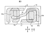
- FIG. 3 is a perspective view of the electronic component 10 seen from above. In FIG. 3, only the inductor conductor layers 18a, 24, and 30a are shown.
- the stacking direction of the stacked body 12 is defined as the vertical direction. One side in the stacking direction is the lower side, and the other side in the stacking direction is the upper side.
- the direction in which the long side of the upper surface of the electronic component 10 extends is defined as the left-right direction, and the direction in which the short side of the upper surface of the electronic component 10 extends is the front-rear direction. It is defined as
- the electronic component 10 includes a multilayer body 12, external electrodes 14a to 14c, inductor conductor layers 18a, 18b, 24, 30a, 30b, capacitor conductor layers 20, 26, 32, 34, ground.
- a conductor layer 22 and via-hole conductors v1 to v9 are provided.
- the laminate 12 has a rectangular parallelepiped shape, and is configured by laminating insulator layers 16a to 16h (an example of a plurality of insulator layers) in this order from the upper side to the lower side. ing.
- the lower surface of the laminated body 12 is a mounting surface.
- the mounting surface is a surface facing the circuit board when the electronic component 10 is mounted on the circuit board.
- the insulator layers 16a to 16h have a rectangular shape with long sides extending in the left-right direction when viewed from above, and are made of, for example, ceramic.
- the top surfaces of the insulator layers 16a to 16h are referred to as front surfaces, and the bottom surfaces of the insulator layers 16a to 16h are referred to as back surfaces.
- the external electrodes 14a, 14c, and 14b are provided so as to be arranged in this order from the left side to the right side on the lower surface of the multilayer body 12, and are not provided on the front surface, the rear surface, the right surface, and the left surface of the multilayer body 12.
- the external electrodes 14a to 14c have a rectangular shape.
- the external electrodes 14a to 14c are produced, for example, by applying Ni plating and Sn plating, or Ni plating and Au plating on a base electrode made of silver or copper.
- Inductor conductor layers 18a and 18b are provided in the left half region of the surfaces of insulator layers 16c and 16d, respectively, and when viewed in plan from above, clockwise direction It is a linear conductor layer that goes around.
- the upstream end of the inductor conductor layers 18a and 18b in the clockwise direction is referred to as an upstream end (an example of a third connection portion), and the downstream end of the inductor conductor layers 18a and 18b in the clockwise direction. Is referred to as a downstream end (an example of a fourth connecting portion).
- the via-hole conductor v2 (an example of the first via-hole conductor) penetrates the insulator layer 16c in the vertical direction, and connects the downstream end of the inductor conductive layer 18a and the upstream end of the inductor conductive layer 18b. Thereby, the inductor conductor layers 18a and 18b and the via-hole conductor v2 are included in the inductor L1.
- the inductor L1 has a spiral shape that proceeds from the upper side to the lower side while rotating in the clockwise direction when viewed from above.
- the capacitor conductor layer 20 (an example of a first capacitor conductor) is provided in the left half region of the surface of the insulator layer 16f and is a rectangular conductor layer.
- the ground conductor layer 22 (an example of the first ground conductor, the second ground conductor, and the third ground conductor) is provided on the surface of the insulator layer 16g and is a conductor layer having a cross shape.
- the ground conductor layer 22 includes a main body portion 22a and branch portions 22b and 22c.
- the main body 22a is provided at the center of the surface of the insulator layer 16g and has a rectangular shape.
- Each of the branch portions 22b and 22c protrudes from the main body portion 22a in the left-right direction.
- the capacitor conductor layer 20 and the branch portion 22b are opposed to each other via the insulator layer 16f. Thereby, the capacitor conductor layer 20 and the ground conductor layer 22 are included in the capacitor C1.
- the via-hole conductor v1 penetrates the insulator layers 16c to 16h in the vertical direction, and connects the upstream end of the inductor conductor layer 18a, the capacitor conductor layer 20, and the external electrode 14a. As a result, the upstream end of the inductor conductor layer 18a is electrically connected to the capacitor conductor layer 20.
- the via-hole conductor v3 passes through the insulator layers 16d to 16f in the vertical direction, and connects the downstream end of the inductor conductor layer 18b and the ground conductor layer 22. Thus, the downstream end of the inductor conductor layer 18b is electrically connected to the capacitor conductor layer 20 via the via-hole conductors v2 and v3 and the inductor conductor layer 18b.
- the via-hole conductor v4 passes through the insulating layers 16g and 16h in the vertical direction, and connects the ground conductor layer 22 and the external electrode 14c. Thereby, the inductor L1 and the capacitor C1 are connected in parallel to form the LC parallel resonator LC1. Furthermore, one end of the LC parallel resonator LC1 is connected to the external electrode 14a, and the other end of the LC parallel resonator LC1 is connected to the external electrode 14c.
- Inductor conductor layers 30a and 30b (an example of a plurality of third inductor conductors), capacitor conductor layer 32 (third capacitor conductor) and via-hole conductors v7 to v9 are inductor conductor layers 18a and 18b, capacitor conductor layer 20 and via holes.
- the conductors v1 to v3 are in a line-symmetric relationship with respect to a straight line extending in the front-rear direction at the center (intersection of diagonal lines) of the multilayer body 12. Therefore, the inductor conductor layers 30a and 30b circulate in the counterclockwise direction when viewed from above.
- the inductor conductor layers 18a and 18b circulate when going from the upstream end to the downstream end (an example of the first direction), and the inductor conductor layers 30a and 30b circulate when going from the upstream end to the downstream end.
- the direction to perform is opposite.
- the upstream end of the inductor conductor layers 30a and 30b in the counterclockwise direction is referred to as an upstream end (an example of a fifth connection portion)
- the downstream end of the inductor conductor layers 30a and 30b in the counterclockwise direction is referred to as an upstream end.
- the end portion is referred to as a downstream end (an example of a sixth connection portion). Further description of the configurations of the inductor conductor layers 30a and 30b, the capacitor conductor layer 32, and the via-hole conductors v7 to v9 is omitted.
- the inductor conductor layers 30a and 30b (an example of the third inductor conductor) and the via-hole conductor v8 (an example of the third via-hole conductor) are included in the inductor L3.
- the capacitor conductor layer 32 and the ground conductor layer 22 are included in the capacitor C3.
- the inductor conductor layer 24 (an example of a second inductor conductor) is a linear conductor layer that is provided on the surface of the insulator layer 16b and has an S shape when viewed from above.
- the inductor conductor layer 24 is included in the inductor L2. Therefore, the inductor conductor layer 24 is provided above the inductor conductor layers 18a, 18b, 30a, and 30b.
- the inductor conductive layer 24 includes a left portion 24a and a right portion 24b. The boundary between the left part 24a and the right part 24b is the center of the insulator layer 16b.
- the left portion 24a is located in the vicinity of the center of the long side on the rear side of the insulator layer 16b from one end (hereinafter referred to as the upstream end) located at the center of the insulator layer 16b when viewed from above. It circulates clockwise to the end (hereinafter referred to as the downstream end).
- a part of the left portion 24a faces a part of the inductor conductor layer 18a via the insulator layer 16b and a part of the capacitor conductor layers 20, 26, 34 when viewed from above. ing.
- a part of the left part 24a, a part of the inductor conductor layer 18a, and a part of the capacitor conductor layers 20, 26, 34 are included in the capacitor C4.
- the right portion 24b is, when viewed from above, from one end located in the vicinity of the center of the long side on the front side of the insulator layer 16b (hereinafter referred to as the upstream end) to the other end located at the center of the insulator layer 16b. It turns around in the counterclockwise direction (hereinafter referred to as the downstream end).
- the upstream end of the left portion 24a and the downstream end of the right portion 24b are connected.
- the upstream end of the right portion 24b is referred to as an upstream end t1 (an example of a first connection portion)
- the downstream end of the left portion 24a is referred to as a downstream end t2 (an example of a second connection portion).
- a part of the right portion 24b faces a part of the inductor conductor layer 30a via the insulator layer 16b and a part of the capacitor conductor layers 26, 32, and 34 when viewed from above. ing.
- a part of the right part 24b, a part of the inductor conductor layer 30a, and a part of the capacitor conductor layers 26, 32, and 34 are included in the capacitor C5.
- the left portion 24a and the right portion 24b are not point-symmetric with respect to the center of the insulating layer 16b when viewed from above. More specifically, the inner diameter of the left portion 24a is smaller than the inner diameter of the right portion 24b. Accordingly, when viewed in plan from above, the area of the region A1 (an example of the first region) surrounded by the inductor conductor layer 18a and the left portion 24a of the inductor conductor layer 24 is the inductor conductor layer 30a and the inductor conductor. The area is smaller than the area A2 (an example of the second area) surrounded by the right portion 24b of the layer 24.
- the region A1 is surrounded by the inductor conductor layer 18a located closest to the inductor conductor layer 24 in the vertical direction (that is, located on the uppermost side of the inductor conductor layers 18a and 18b).
- the region A2 is surrounded by the inductor conductor layer 30a located closest to the inductor conductor layer 24 in the vertical direction (that is, located on the uppermost side of the inductor conductor layers 30a and 30b).
- a portion surrounding the region A1 in the left portion 24a is referred to as a region forming portion 50a (an example of a first region forming portion), and a portion surrounding the region A2 in the right portion 24b is referred to as a region forming portion 50b.
- This is called (an example of a second region forming portion).
- the region forming part 50a is a part in contact with the region A1
- the region forming part 50b is a part in contact with the region A2.
- the region forming part 50b and the region forming part 50a are electrically connected in series in this order in the path from the upstream end t1 to the downstream end t2.
- the direction in which the inductor conductor layer 18a circulates when going from the upstream end to the downstream end is the direction in which the region forming portion 50a circulates when going from the upstream end t1 to the downstream end t2. It is the same as (an example of the second direction) and is the clockwise direction. Thereby, the direction of the current flowing through the inductor conductor layer 18a and the direction of the current flowing through the region forming portion 50a coincide.
- the direction in which the inductor conductor layer 30a circulates when going from the upstream end to the downstream end is the direction in which the region forming portion 50b circulates when going from the upstream end t1 to the downstream end t2.
- the direction of the current flowing through the inductor conductor layer 30a matches the direction of the current flowing through the region forming portion 50b.
- the direction of the current flowing through the inductor conductor layer 18a and the region forming portion 50a is opposite to the direction of the current flowing through the inductor conductor layer 30a and the region forming portion 50b.
- the capacitor conductor layer 26 (an example of a second capacitor conductor) is a rectangular conductor layer provided at the center of the surface of the insulator layer 16f.
- the capacitor conductor layer 26 and the main body portion 22a of the ground conductor layer 22 are opposed to each other through the insulator layer 16f. Thereby, the capacitor conductor layer 26 and the ground conductor layer 22 are included in the capacitor C2.
- the via-hole conductor v5 passes through the insulator layers 16b to 16e in the vertical direction, and connects the upstream end t1 of the inductor conductor layer 24 and the capacitor conductor layer 26. That is, the upstream end t ⁇ b> 1 of the inductor conductive layer 24 is electrically connected to the capacitor conductive layer 26.
- the via-hole conductor v6 passes through the insulator layers 16b to 16f in the vertical direction, and connects the downstream end t2 of the inductor conductor layer 24 and the ground conductor layer 22. That is, the downstream end t ⁇ b> 2 of the inductor conductor layer 24 is electrically connected to the ground conductor layer 22.
- the inductor L2 and the capacitor C2 are connected in parallel to configure the LC parallel resonator LC2. Furthermore, since the via-hole conductor v4 connects the ground conductor layer 22 and the external electrode 14c, the other end of the LC parallel resonator LC2 is electrically connected to the external electrode 14c.
- the capacitor conductor layer 34 is a belt-like conductor layer provided on the surface of the insulator layer 16e and extending in the left-right direction.
- the capacitor conductor layer 34 is opposed to the capacitor conductor layers 20 and 32 via the insulator layer 16e. Thereby, a capacitance is formed between the capacitor conductor layer 20 and the capacitor conductor layer 32 via the capacitor conductor layer 34. Therefore, the capacitor conductor layers 20, 32, and 34 are included in the capacitor C6.
- the inductor conductor layers 18a, 18b, 24, 30a, 30b, the capacitor conductor layers 20, 26, 32, 34, the ground conductor layer 22, and the via-hole conductors v1 to v9 are made of, for example, a conductive material such as silver or copper. .
- the inductor conductor layer 24 has an upstream end t1 electrically connected to the capacitor conductor layer 26 and a downstream end t2 electrically connected to the ground conductor layer 22. Therefore, the direction of the current flowing in the via-hole conductor v5 connected to the upstream end t1 is different from the direction of the current flowing in the via-hole conductor v9.
- capacitive coupling is stronger than inductive coupling, and the direction of the current flowing in the via-hole conductor v6 connected to the downstream end t2 and the current flowing in the via-hole conductor v3 are Since the directions are the same, the magnetic flux generated in the via-hole conductor v6 and the magnetic flux generated in the via-hole conductor v3 are in the same direction, so that the region forming portion 50a near the downstream end t2 is more inductive than capacitive coupling. The bond becomes stronger. Therefore, the region forming portion 50a and the inductor conductor layer 18a are easily magnetically coupled.
- the area A1 surrounded by the inductor conductor layer 18a and the inductor conductor layer 24 is surrounded by the inductor conductor layer 30a and the inductor conductor layer 24.
- the area is smaller than the area A2.
- the magnetic coupling between the region forming portion 50a and the inductor conductor layer 18a is suppressed.
- the strength of the magnetic coupling between the region forming portion 50a and the inductor conductor layer 18a approaches the strength of the magnetic coupling between the region forming portion 50b and the inductor conductor layer 30a. Therefore, the input impedance measured from the external electrode 14a approaches the input impedance measured from the external electrode 14b.
- FIG. 4 is a perspective view of the electronic component 110 according to the comparative example from above.
- the reference number corresponding to the electronic component 10 is obtained by adding 100 to the reference number of each component of the electronic component 10.
- a first model and a second model having respective configurations of the electronic components 10 and 110 were created.
- the electronic component 110 is different from the electronic component 10 in the shape of the inductor conductor layer 124. More specifically, the inductor conductor layer 124 has a point-symmetric structure. Therefore, the area of the region A11 surrounded by the inductor conductive layer 124 and the inductor conductive layer 118a is equal to the area of the region A12 surrounded by the inductor conductive layer 124 and the inductor conductive layer 130a.
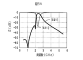
- FIG. 5A is a graph showing the transmission characteristic
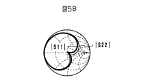
- FIG. 5B is a Smith chart showing the input impedance of the first model. In the Smith chart of FIG. 5B, the frequency of the high-frequency signal was changed from 0.5 GHz to 5.5 GHz.
- FIG. 5C is a graph showing the transmission characteristic
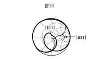
- 5D is a Smith chart showing the input impedance of the second model.
- the frequency of the high frequency signal was changed from 0.5 GHz to 6.0 GHz.
- shaft shows a transmission characteristic and a reflection characteristic
- a horizontal axis shows a frequency.
- FIG. 5D shows that in the second model, the impedance change on the external electrode 114a (not shown) side does not match the impedance change on the external electrode 114b (not shown) side.
- FIG. 5B shows that in the first model, the change in impedance on the external electrode 14a side matches the change in impedance on the external electrode 14b side.
- the reflection characteristic of the electronic component 10 is smaller than the reflection characteristic of the electronic component 110 in the passband (2.2 GHz to 3.0 GHz).
- the input impedance measured from the external electrode 14a approaches the input impedance measured from the external electrode 14b, and impedance matching is achieved, thereby suppressing reflection of high-frequency signals in the passband.
- the inductor conductor layer 24 is suppressed from being magnetically coupled to conductor layers other than the inductor conductor layers 18a and 30a. More specifically, the region A1 is surrounded by the inductor conductor layer 18a positioned closest to the inductor conductor layer 24 in the vertical direction. The region A2 is surrounded by the inductor conductor layer 30a located closest to the inductor conductor layer 24 in the vertical direction. Thereby, the inductor conductor layer 24 is magnetically coupled to the inductor conductor layers 18a and 30a. Therefore, the inductor conductor layer 24 is less likely to be magnetically coupled to the conductor layer below the inductor conductor layers 18a and 30a.
- FIG. 6 is an exploded perspective view of an electronic component 10a according to a modification.
- FIG. 7 is a perspective view of the electronic component 10a seen from above.
- the electronic component 10a differs from the electronic component 10 in two points: the direction of the LC parallel resonator LC3 and the shape of the inductor conductor layer 24 ′. More specifically, when viewed from above, the inductor conductor layers 30a and 30b and the via-hole conductors v7 to v9 in the electronic component 10a are 180 ° apart from the inductor conductor layers 30a and 30b and the via-hole conductors v7 to v9 in the electronic component 10. It is obtained by rotating.
- the inductor conductor layers 30a and 30b, the capacitor conductor layer 32, and the via-hole conductors v7 to v9 are viewed from above with the inductor conductor layers 18a and 18b, the capacitor conductor layer 20, and the via-hole conductors v1 to v3.
- it is point-symmetric with respect to the center of the laminate 12 (intersection of diagonal lines). Accordingly, the inductor conductor layers 18a and 18b circulate when going from the upstream end to the downstream end (an example of the first direction), and the inductor conductor layers 30a and 30b circulate when going from the upstream end to the downstream end.
- the direction to perform is the same.
- the inductor conductor layer 24 ′ is a linear conductor layer provided on the surface of the insulator layer 16b, and has a shape in which a part of a rectangle is cut out.
- the inductor conductor layer 24 ′ is included in the inductor L2, and includes a left portion 24a ′ and a right portion 24b ′.
- the left portion 24a ′ is a long side on the back side of the insulator layer 16b from one end (hereinafter referred to as an upstream end) located near the center of the long side on the front side of the insulator layer 16b when viewed from above.
- the other end (hereinafter referred to as the downstream end) located in the vicinity of the center of the center is rotated in the clockwise direction.
- the right portion 24b ' is located in the vicinity of the center of the long side on the front side of the insulator layer 16b from one end (hereinafter referred to as the upstream end) located at the center of the insulator layer 16b when viewed from above. It circulates clockwise to the end (hereinafter referred to as the downstream end).
- the upstream end of the left portion 24a ′ and the downstream end of the right portion 24b ′ are connected.
- the upstream end of the right portion 24b ′ is referred to as an upstream end t1
- the downstream end of the left portion 24a ′ is referred to as a downstream end t2.
- the upstream end t1 is connected to the capacitor conductor layer 26 via the via-hole conductor v5.
- the downstream end t2 is connected to the ground conductor layer 22 via the via-hole conductor v6.
- the left portion 24a ′ and the right portion 24b ′ have a line-symmetric relationship with respect to a straight line passing through the center of the insulator layer 16b in the front-rear direction when viewed from above. It is not. More specifically, the inner diameter of the left portion 24a ′ is smaller than the inner diameter of the right portion 24b ′. Thereby, when viewed in plan from above, the area of the region A1 surrounded by the inductor conductor layer 18a and the left portion 24a ′ of the inductor conductor layer 24 ′ is the right of the inductor conductor layer 30a and the inductor conductor layer 24 ′. It is smaller than the area of the region A2 surrounded by the portion 24b ′.
- a portion surrounding the region A1 is referred to as a region forming portion 50a ′
- a portion surrounding the region A2 is referred to as a region forming portion 50b ′.
- the region forming part 50b ′ and the region forming part 50a ′ are electrically connected in series in this order in the path from the upstream end t1 to the downstream end t2.
- the direction in which the inductor conductor layer 18a circulates when going from the upstream end to the downstream end is that the region forming portion 50a ′ circulates when going from the upstream end t1 to the downstream end t2. It is the same as the direction (an example of the second direction) and is the clockwise direction. As a result, the direction of the current flowing through the inductor conductor layer 18a matches the direction of the current flowing through the region forming portion 50a ′.
- the region forming portion 50b in the direction in which the inductor conductor layer 30a circulates when going from the upstream end to the downstream end (an example of the third direction), the region forming portion 50b 'circulates when going from the upstream end t1 to the downstream end t2. It is the same as the direction (an example of the fourth direction) and is the clockwise direction. As a result, the direction of the current flowing through the inductor conductor layer 30a and the direction of the current flowing through the region forming portion 50b ′ coincide. In addition, the direction of the current flowing through the inductor conductor layer 18a and the region forming portion 50a ′ is the same as the direction of the current flowing through the inductor conductor layer 30a and the region forming portion 50b ′.
- the electronic component 10 a configured as described above can also exhibit the same effects as the electronic component 10.
- the electronic component according to the present invention is not limited to the electronic components 10 and 10a, and can be changed within the scope of the gist thereof.
- the inductor L1 may include only one inductor conductor layer 18a.
- the inductor L2 may include only one inductor conductor layer 30a.
- the electronic components 10 and 10a include the three-stage LC parallel resonator, but may include four or more LC parallel resonators.
- the external electrodes 14a to 14c may be provided not only on the lower surface of the multilayer body 12, but also on the front surface, rear surface, left surface, right surface, upper surface, and lower surface of the multilayer body 12.
- the external electrode 14a may cover the front surface of the left surface of the multilayer body 12 and may cover a part of the front surface, the rear surface, the upper surface, and the lower surface.
- the external electrode 14b may cover the front surface of the right surface of the multilayer body 12 and may cover a part of the front surface, the rear surface, the upper surface, and the lower surface.
- the via-hole conductors v1 and v7 are unnecessary, and the upstream ends of the inductor conductor layers 18a and 30a can be directly connected to the external electrodes 14a and 14b.
- the inductor conductor layers 24 and 24 ′ may be provided below the inductor conductor layers 18b and 30b. In this case, the inductor conductor layers 24 and 24 ′ are magnetically coupled to the inductor conductor layers 18b and 30b.
- via-hole conductors v1, v2, v3, v5, v6, v7, and v8 may not be connected to the end portions of the inductor conductor layers 18a, 18b, 24, 30a, and 30b.
- the inductors L1 and L3 may have a shape other than a spiral shape.
- the present invention is useful for electronic components, and is particularly excellent in that it can suppress the occurrence of a shift in input impedance measured from each input / output terminal.
Landscapes
- Engineering & Computer Science (AREA)
- Power Engineering (AREA)
- Microelectronics & Electronic Packaging (AREA)
- Coils Or Transformers For Communication (AREA)
- Filters And Equalizers (AREA)
- Manufacturing & Machinery (AREA)
Abstract
2つのLC並列共振器の特性インピーダンスにずれが発生することを抑制することである。 本発明に係る電子部品は、第2のインダクタは、第2のコンデンサ導体に電気的に接続される第1の接続部及び第2のグランド導体に電気的に接続される第2の接続部を有する第2のインダクタ導体を含んでおり、積層方向から平面視したときに、第1のインダクタ導体と第2のインダクタ導体とにより囲まれている第1の領域の面積は、第3のインダクタ導体層と第2のインダクタ導体とにより囲まれている第2の領域の面積よりも小さく、第2のインダクタ導体において第2の領域を囲んでいる第2の領域形成部及び第2のインダクタ導体において第1の領域を囲んでいる第1の領域形成部は、第1の接続部から第2の接続部へと向かう経路においてこの順に電気的に直列に接続されていること、を特徴とする。
Description
本発明は、電子部品に関し、より特定的には、第1のLC並列共振器ないし第3のLC並列共振器を備えた電子部品に関する。
従来の電子部品に関する発明としては、例えば、特許文献1に記載の積層帯域通過フィルタが知られている。該積層帯域通過フィルタは、第1のLC並列共振器ないし第3のLC並列共振器を備えている。第1のLC並列共振器は、左側が開口した角張ったU字型の第1のインダクタ電極を備えている。第2のLC並列共振器は、右側が開口した角張ったU字型の第2のインダクタ電極を備えている。第1のインダクタ電極と第2のインダクタ電極とは、線対称な関係にある。
第3のLC並列共振器は、第3のインダクタ電極を備えている。第3のインダクタ電極は、第1のインダクタ電極及び第2のインダクタ電極よりも下側に設けられており、上側から平面視したときに、第1のインダクタ電極及び第2のインダクタ電極に重なっている。第1のインダクタ電極と第3のインダクタ電極とに囲まれた第1の領域の面積と第2のインダクタ電極と第3のインダクタ電極とに囲まれた第2の領域の面積とは等しい。以上のような第1のLC並列共振器ないし第3のLC並列共振器は、バンドパスフィルタを構成している。
ところで、特許文献1に記載の積層帯域通過フィルタでは、第1のLC並列共振器側の入出力端子から見た特性インピーダンスと、第3のLC並列共振器側の入出力端子から見た特性インピーダンスとがずれる。より詳細には、第1のインダクタ電極と第3のインダクタ電極とに囲まれた第1の領域の面積と第2のインダクタ電極と第3のインダクタ電極とに囲まれた第2の領域の面積とは等しい。これは、第1のインダクタ電極と第3のインダクタ電極との磁気結合の強さと、第2のインダクタ電極と第3のインダクタ電極との磁気結合の強さとを近づけるためである。
ただし、第3のインダクタ電極の一端がグランド電極に電気的に接続される。第1の領域を囲む部分は、第3のインダクタ電極の一端の近傍に位置している。そのため、第3のインダクタ電極における第1の領域を囲む部分では、誘導性の結合が強くなる。一方、第3のインダクタ電極の他端がコンデンサ電極に電気的に接続される。第2の領域を囲む部分は、第3のインダクタ電極の他端の近傍に位置している。そのため、第3のインダクタ電極における第2の領域を囲む部分では、容量性の結合が強くなる。その結果、第1のインダクタ電極と第3のインダクタ電極との磁気結合は、第2のインダクタ電極と第3のインダクタ電極との磁気結合よりも強くなってしまう。その結果、特許文献1に記載の積層帯域通過フィルタでは、第1のLC並列共振器側の入出力端子から見た特性インピーダンスと、第3のLC並列共振器側の入出力端子から見た入力インピーダンスとがずれる。
そこで、本発明の目的は、それぞれの入出力端子から測定した入力インピーダンスにずれが発生することを抑制できる電子部品を提供することである。
本発明の一形態に係る電子部品は、複数の絶縁体層が積層方向に積層されて構成されている積層体と、第1のLC並列共振器、第2のLC並列共振器及び第3のLC並列共振器と、を備えており、前記第1のLC並列共振器は、第1のインダクタと第1のコンデンサを含んでおり、前記第3のLC並列共振器は、第3のインダクタと第3のコンデンサを含んでおり、前記第2のLC並列共振器は、互いに並列に接続される第2のインダクタ及び第2のコンデンサを含んでおり、前記第1のインダクタ及び第3のインダクタはそれぞれ、前記積層方向から平面視したときに、周回する第1のインダクタ導体及び第3のインダクタ導体を含んでおり、前記第2のコンデンサは、互いに対向する第2のコンデンサ導体と第2のグランド導体とを含んでおり、前記第2のインダクタは、前記第2のコンデンサ導体に電気的に接続される第1の接続部及び前記第2のグランド導体に電気的に接続される第2の接続部を有する第2のインダクタ導体を含んでおり、前記積層方向から平面視したときに、前記第1のインダクタ導体と前記第2のインダクタ導体とにより囲まれている第1の領域の面積は、前記第3のインダクタ導体と該第2のインダクタ導体とにより囲まれている第2の領域の面積よりも小さく、前記第2のインダクタ導体において前記第2の領域を囲んでいる第2の領域形成部及び該第2のインダクタ導体において前記第1の領域を囲んでいる第1の領域形成部は、前記第1の接続部から前記第2の接続部へと向かう経路においてこの順に電気的に直列に接続されていること、を特徴とする。
本発明によれば、各々の入出力端子から測定した入力インピーダンスのずれが発生することを抑制できる。
以下に、本発明の実施形態に係る電子部品について図面を参照しながら説明する。
(電子部品の構成)
まず、一実施形態に係る電子部品10の回路構成について図面を参照しながら説明する。図1は、一実施形態に係る電子部品10の等価回路図である。
まず、一実施形態に係る電子部品10の回路構成について図面を参照しながら説明する。図1は、一実施形態に係る電子部品10の等価回路図である。
電子部品10は、バンドパスフィルタであり、図1に示すように、LC並列共振器LC1~LC3、コンデンサC4~C6及び外部電極14a~14cを備えている。
外部電極14a,14bは、高周波信号の入出力端子である。外部電極14cは、接地電位に接続されるグランド端子である。
コンデンサC4,C5は、外部電極14aと外部電極14bとの間において、この順に直列に接続されている。また、コンデンサC6は、コンデンサC4,C5に対して並列に接続されている。
LC並列共振器LC1(第1のLC並列共振器の一例)は、互いに並列に接続されているインダクタL1(第1のインダクタの一例)及びコンデンサC1(第1のコンデンサの一例)を含んでいる。LC並列共振器LC1の一端は、外部電極14aとコンデンサC4との間の部分に接続されている。LC並列共振器LC1の他端は、外部電極14cに接続されている。
LC並列共振器LC2(第2のLC並列共振器の一例)は、互いに並列に接続されているインダクタL2(第2のインダクタの一例)及びコンデンサC2(第2のコンデンサの一例)を含んでいる。LC並列共振器LC2の一端は、コンデンサC4とコンデンサC5との間の部分に接続されている。LC並列共振器LC2の他端は、外部電極14cに接続されている。
LC並列共振器LC3(第3のLC並列共振器の一例)は、互いに並列に接続されているインダクタL3(第3のインダクタの一例)及びコンデンサC3(第3のコンデンサの一例)を含んでいる。LC並列共振器LC3の一端は、コンデンサC5と外部電極14bとの間の部分に接続されている。LC並列共振器LC3の他端は、外部電極14cに接続されている。
また、インダクタL1とインダクタL2とは磁気結合している。インダクタL2とインダクタL3とは磁気結合している。
以上のように構成された電子部品10は、バンドパスフィルタとして機能する。より詳細には、LC並列共振器LC1~LC3のインピーダンスは、これらの共振周波数において最大となる。そのため、LC並列共振器LC1~LC3は、これらの共振周波数付近の周波数を有する高周波信号を通過させない。すなわち、LC並列共振器LC1~LC3の共振周波数付近の周波数を有する高周波信号は、外部電極14a,14bから外部電極14cへと流れずに、外部電極14aと外部電極14bとの間を流れる。一方、LC並列共振器LC1~LC3の共振周波数付近の周波数外の周波数では、LC並列共振器LC1~LC3のインピーダンスは比較的に低い。そのため、LC並列共振器LC1~LC3の共振周波数付近の周波数外の周波数は、LC並列共振器LC1~LC3を通過して、外部電極14cを介してグランドへと流れる。以上のように、電子部品10では、LC並列共振器LC1~LC3の共振周波数付近の周波数の高周波信号のみを通過させるバンドパスフィルタとして機能する。
(電子部品の具体的構成)
次に、電子部品10の具体的な構成について図面を参照しながら説明する。図2は、電子部品10の分解斜視図である。図3は、電子部品10を上側から透視した図である。図3では、インダクタ導体層18a,24,30aのみを示した。電子部品10において、積層体12の積層方向を上下方向と定義する。積層方向の一方側が下側であり、積層方向の他方側が上側である。また、電子部品10を上側から平面視したときに、電子部品10の上面の長辺が延在する方向を左右方向と定義し、電子部品10の上面の短辺が延在する方向を前後方向と定義する。
次に、電子部品10の具体的な構成について図面を参照しながら説明する。図2は、電子部品10の分解斜視図である。図3は、電子部品10を上側から透視した図である。図3では、インダクタ導体層18a,24,30aのみを示した。電子部品10において、積層体12の積層方向を上下方向と定義する。積層方向の一方側が下側であり、積層方向の他方側が上側である。また、電子部品10を上側から平面視したときに、電子部品10の上面の長辺が延在する方向を左右方向と定義し、電子部品10の上面の短辺が延在する方向を前後方向と定義する。
電子部品10は、図2及び図3に示すように、積層体12、外部電極14a~14c、インダクタ導体層18a,18b,24,30a,30b、コンデンサ導体層20,26,32,34、グランド導体層22及びビアホール導体v1~v9を備えている。
積層体12は、図2に示すように、直方体状をなしており、絶縁体層16a~16h(複数の絶縁体層の一例)が上側から下側へとこの順に積層されることにより構成されている。積層体12の下面は、実装面である。実装面は、電子部品10の回路基板への実装時に回路基板に対向する面である。
絶縁体層16a~16hは、上側から平面視したときに、左右方向に延在する長辺を有する長方形状をなしており、例えば、セラミック等により作製されている。以下では、絶縁体層16a~16hの上面を表面と呼び、絶縁体層16a~16hの下面を裏面と呼ぶ。
外部電極14a,14c,14bは、積層体12の下面において左側から右側へとこの順に並ぶように設けられており、積層体12の前面、後面、右面及び左面には設けられていない。外部電極14a~14cは、長方形状をなしている。外部電極14a~14cは、例えば、銀又は銅からなる下地電極上にNiめっき及びSnめっき、又は、Niめっき及びAuめっきが施されることにより作製されている。
インダクタ導体層18a,18b(複数の第1のインダクタ導体の一例)はそれぞれ、絶縁体層16c,16dの表面の左半分の領域に設けられており、上側から平面視したときに、時計回り方向に周回する線状の導体層である。以下では、インダクタ導体層18a,18bの時計回り方向の上流側の端部を上流端(第3の接続部の一例)と呼び、インダクタ導体層18a,18bの時計回り方向の下流側の端部を下流端(第4の接続部の一例)と呼ぶ。
ビアホール導体v2(第1のビアホール導体の一例)は、絶縁体層16cを上下方向に貫通しており、インダクタ導体層18aの下流端とインダクタ導体層18bの上流端とを接続している。これにより、インダクタ導体層18a,18b及びビアホール導体v2は、インダクタL1に含まれている。インダクタL1は、上側から平面視したときに、時計回り方向に周回しながら上側から下側へと進行する螺旋状をなしている。
コンデンサ導体層20(第1のコンデンサ導体の一例)は、絶縁体層16fの表面の左半分の領域に設けられており、長方形状をなす導体層である。グランド導体層22(第1のグランド導体、第2のグランド導体及び第3のグランド導体の一例)は、絶縁体層16gの表面に設けられており、十字型をなす導体層である。グランド導体層22は、本体部22a及び枝部22b,22cを含んでいる。本体部22aは、絶縁体層16gの表面の中央に設けられており、長方形状をなしている。枝部22b,22cはそれぞれ、本体部22aから左右方向に突出している。また、コンデンサ導体層20と枝部22bとは、絶縁体層16fを介して互いに対向している。これにより、コンデンサ導体層20及びグランド導体層22は、コンデンサC1に含まれている。
ビアホール導体v1は、絶縁体層16c~16hを上下方向に貫通しており、インダクタ導体層18aの上流端とコンデンサ導体層20と外部電極14aとを接続している。これにより、インダクタ導体層18aの上流端は、コンデンサ導体層20に電気的に接続されている。また、ビアホール導体v3は、絶縁体層16d~16fを上下方向に貫通しており、インダクタ導体層18bの下流端とグランド導体層22とを接続している。これにより、インダクタ導体層18bの下流端は、ビアホール導体v2,v3及びインダクタ導体層18bを介してコンデンサ導体層20に電気的に接続されている。また、ビアホール導体v4は、絶縁体層16g,16hを上下方向に貫通しており、グランド導体層22と外部電極14cとを接続している。これにより、インダクタL1とコンデンサC1とが並列に接続されてLC並列共振器LC1を構成している。更に、LC並列共振器LC1の一端が外部電極14aに接続され、LC並列共振器LC1の他端が外部電極14cに接続されている。
インダクタ導体層30a,30b(複数の第3のインダクタ導体の一例)、コンデンサ導体層32(第3のコンデンサ導体)及びビアホール導体v7~v9は、インダクタ導体層18a,18b、コンデンサ導体層20及びビアホール導体v1~v3と、上側から平面視したときに、積層体12の中央(対角線の交点)を前後方向に延在する直線に関して線対称な関係にある。したがって、インダクタ導体層30a,30bは、上側から平面視したときに、反時計回り方向に周回している。よって、上流端から下流端へと向かうときにインダクタ導体層18a,18bが周回する方向(第1の方向の一例)と、上流端から下流端へと向かうときにインダクタ導体層30a,30bが周回する方向(第3の方向の一例)とは、逆である。以下では、インダクタ導体層30a,30bの反時計回り方向の上流側の端部を上流端(第5の接続部の一例)と呼び、インダクタ導体層30a,30bの反時計回り方向の下流側の端部を下流端(第6の接続部の一例)と呼ぶ。なお、インダクタ導体層30a,30b、コンデンサ導体層32及びビアホール導体v7~v9の構成についてはこれ以上の説明を省略する。
インダクタ導体層30a,30b(第3のインダクタ導体の一例)及びビアホール導体v8(第3のビアホール導体の一例)は、インダクタL3に含まれている。コンデンサ導体層32及びグランド導体層22は、コンデンサC3に含まれている。
インダクタ導体層24(第2のインダクタ導体の一例)は、絶縁体層16bの表面に設けられており、上側から見たときに、S字状をなす線状の導体層である。インダクタ導体層24は、インダクタL2に含まれている。よって、インダクタ導体層24は、インダクタ導体層18a,18b,30a,30bよりも上側に設けられている。インダクタ導体層24は、左部24a及び右部24bを含んでいる。左部24aと右部24bとの境界は、絶縁体層16bの中央である。
左部24aは、上側から平面視したときに、絶縁体層16bの中央に位置する一端(以下では、上流端と称す)から絶縁体層16bの後ろ側の長辺の中央近傍に位置する他端(以下では、下流端と称す)まで時計回り方向に周回している。また、左部24aの一部は、上側から平面視したときに、インダクタ導体層18aの一部と絶縁体層16bを介して対向し、コンデンサ導体層20,26,34の一部とも対向している。これにより、左部24aの一部、インダクタ導体層18aの一部及びコンデンサ導体層20,26,34の一部は、コンデンサC4に含まれている。
右部24bは、上側から平面視したときに、絶縁体層16bの前側の長辺の中央近傍に位置する一端(以下では、上流端と称す)から絶縁体層16bの中央に位置する他端(以下では、下流端と称す)まで反時計回り方向に周回している。左部24aの上流端と右部24bの下流端とは接続されている。以下では、右部24bの上流端を上流端t1(第1の接続部の一例)と呼び、左部24aの下流端を下流端t2(第2の接続部の一例)と呼ぶ。また、右部24bの一部は、上側から平面視したときに、インダクタ導体層30aの一部と絶縁体層16bを介して対向し、コンデンサ導体層26,32,34の一部とも対向している。これにより、右部24bの一部、インダクタ導体層30aの一部及びコンデンサ導体層26,32,34の一部は、コンデンサC5に含まれている。
また、図2及び図3に示すように、左部24aと右部24bとは、上側から平面視したときに、絶縁体層16bの中央に関して点対称な関係にはなっていない。より詳細には、左部24aの内径は、右部24bの内径よりも小さい。したがって、上側から平面視したときに、インダクタ導体層18aとインダクタ導体層24の左部24aとにより囲まれている領域A1の面積(第1の領域の一例)は、インダクタ導体層30aとインダクタ導体層24の右部24bとにより囲まれている領域A2(第2の領域の一例)の面積よりも小さい。領域A1は、上下方向においてインダクタ導体層24の最も近くに位置する(すなわち、インダクタ導体層18a,18bの内の最も上側に位置する)インダクタ導体層18aにより囲まれている。領域A2は、上下方向においてインダクタ導体層24の最も近くに位置する(すなわち、インダクタ導体層30a,30bの内の最も上側に位置する)インダクタ導体層30aにより囲まれている。
以下では、左部24aにおいて、領域A1を囲んでいる部分を領域形成部50a(第1の領域形成部の一例)と呼び、右部24bにおいて、領域A2を囲んでいる部分を領域形成部50b(第2の領域形成部の一例)と呼ぶ。領域形成部50aは、領域A1に接している部分であり、領域形成部50bは、領域A2に接している部分である。領域形成部50b及び領域形成部50aは、上流端t1から下流端t2へと向かう経路においてこの順に電気的に直列に接続されている。
また、上流端から下流端へと向かうときにインダクタ導体層18aが周回する方向(第1の方向の一例)は、上流端t1から下流端t2へと向かうときに領域形成部50aが周回する方向(第2の方向の一例)と同じであり、時計回り方向である。これにより、インダクタ導体層18aに流れる電流の方向と領域形成部50aに流れる電流の方向とが一致する。
更に、上流端から下流端へと向かうときにインダクタ導体層30aが周回する方向(第3の方向の一例)は、上流端t1から下流端t2へと向かうときに領域形成部50bが周回する方向(第4の方向の一例)と同じであり、反時計回り方向である。これにより、インダクタ導体層30aに流れる電流の方向と領域形成部50bに流れる電流の方向とが一致する。また、インダクタ導体層18a及び領域形成部50aに流れる電流の方向とインダクタ導体層30a及び領域形成部50bに流れる電流の方向とが逆になる。
コンデンサ導体層26(第2のコンデンサ導体の一例)は、絶縁体層16fの表面の中央に設けられている長方形状の導体層である。コンデンサ導体層26とグランド導体層22の本体部22aとは、絶縁体層16fを介して対向している。これにより、コンデンサ導体層26及びグランド導体層22は、コンデンサC2に含まれている。
ビアホール導体v5は、絶縁体層16b~16eを上下方向に貫通しており、インダクタ導体層24の上流端t1とコンデンサ導体層26とを接続している。すなわち、インダクタ導体層24の上流端t1は、コンデンサ導体層26と電気的に接続されている。ビアホール導体v6は、絶縁体層16b~16fを上下方向に貫通しており、インダクタ導体層24の下流端t2とグランド導体層22とを接続している。すなわち、インダクタ導体層24の下流端t2は、グランド導体層22と電気的に接続されている。これにより、インダクタL2とコンデンサC2とが並列に接続されてLC並列共振器LC2を構成している。更に、ビアホール導体v4がグランド導体層22と外部電極14cとを接続しているので、LC並列共振器LC2の他端が外部電極14cに電気的に接続されている。
コンデンサ導体層34は、絶縁体層16eの表面に設けられており、左右方向に延在する帯状の導体層である。コンデンサ導体層34は、絶縁体層16eを介してコンデンサ導体層20,32と対向している。これにより、コンデンサ導体層20とコンデンサ導体層32との間には、コンデンサ導体層34を介して容量が形成されている。したがって、コンデンサ導体層20,32,34は、コンデンサC6に含まれている。
インダクタ導体層18a,18b,24,30a,30b、コンデンサ導体層20,26,32,34、グランド導体層22及びビアホール導体v1~v9は、例えば、銀や銅等の導電性材料により作製される。
(効果)
電子部品10によれば、外部電極14aから測定した入力インピーダンスと外部電極14bから測定した入力インピーダンスとにずれが発生することを抑制できる。より詳細には、インダクタ導体層24は、コンデンサ導体層26に電気的に接続される上流端t1及びグランド導体層22に電気的に接続される下流端t2を有している。したがって、上流端t1に接続するビアホール導体v5に流れる電流の向きとビアホール導体v9に流れる電流の向きが異なることから、ビアホール導体v5に発生する磁束とビアホール導体v9に発生する磁束がお互いに打ち消す方向になり、上流端t1の近傍の領域形成部50bでは誘導性の結合よりも容量性の結合が強くなり、下流端t2に接続するビアホール導体v6に流れる電流の向きとビアホール導体v3に流れる電流の向きが同じであることから、ビアホール導体v6に発生する磁束とビアホール導体v3に発生する磁束が同じ方向になることから、下流端t2の近傍の領域形成部50aでは容量性の結合よりも誘導性の結合が強くなる。したがって、領域形成部50aとインダクタ導体層18aとが磁気結合しやすくなる。
電子部品10によれば、外部電極14aから測定した入力インピーダンスと外部電極14bから測定した入力インピーダンスとにずれが発生することを抑制できる。より詳細には、インダクタ導体層24は、コンデンサ導体層26に電気的に接続される上流端t1及びグランド導体層22に電気的に接続される下流端t2を有している。したがって、上流端t1に接続するビアホール導体v5に流れる電流の向きとビアホール導体v9に流れる電流の向きが異なることから、ビアホール導体v5に発生する磁束とビアホール導体v9に発生する磁束がお互いに打ち消す方向になり、上流端t1の近傍の領域形成部50bでは誘導性の結合よりも容量性の結合が強くなり、下流端t2に接続するビアホール導体v6に流れる電流の向きとビアホール導体v3に流れる電流の向きが同じであることから、ビアホール導体v6に発生する磁束とビアホール導体v3に発生する磁束が同じ方向になることから、下流端t2の近傍の領域形成部50aでは容量性の結合よりも誘導性の結合が強くなる。したがって、領域形成部50aとインダクタ導体層18aとが磁気結合しやすくなる。
そこで、電子部品10では、上側から平面視したときに、インダクタ導体層18aとインダクタ導体層24とにより囲まれている領域A1の面積は、前記インダクタ導体層30aとインダクタ導体層24とにより囲まれている領域A2の面積よりも小さい。これにより、領域形成部50aとインダクタ導体層18aとが磁気結合することが抑制される。その結果、領域形成部50aとインダクタ導体層18aとの磁気結合の強さと領域形成部50bとインダクタ導体層30aとの磁気結合の強さとが近づく。よって、外部電極14aから測定した入力インピーダンスと外部電極14bから測定した入力インピーダンスとが近づくようになる。
本願発明者は、電子部品10が奏する効果をより明確にするために、以下に説明するコンピュータシミュレーションを行った。図4は、比較例に係る電子部品110を上側から透視した図である。電子部品110において電子部品10に対応する構成の参照符号には、電子部品10の各構成の参照符号に100を足したものを用いた。
具体的には、電子部品10,110のそれぞれの構成を有する第1のモデル及び第2のモデルを作成した。電子部品110は、インダクタ導体層124の形状において電子部品10と相違する。より詳細には、インダクタ導体層124は、点対称な構造を有している。そのため、インダクタ導体層124とインダクタ導体層118aとにより囲まれた領域A11の面積とインダクタ導体層124とインダクタ導体層130aとにより囲まれた領域A12の面積とは等しい。
本願発明者は、第1のモデル及び第2のモデルの通過特性|S21|及び反射特性|S11|をコンピュータに演算させると共に、外部電極14a,114a側及び外部電極14b,114b側から見た入力インピーダンスを演算させた。図5Aは、第1のモデルの通過特性|S21|及び反射特性|S11|を示したグラフである。図5Bは、第1のモデルの入力インピーダンスをスミスチャートに表示したものである。図5Bのスミスチャートでは、高周波信号の周波数を0.5GHzから5.5GHzまで変化させた。図5Cは、第2のモデルの通過特性|S21|及び反射特性|S11|を示したグラフである。図5Dは、第2のモデルの入力インピーダンスをスミスチャートに表示したものである。図5Cのスミスチャートでは、高周波信号の周波数を0.5GHzから6.0GHzまで変化させた。図5A及び図5Cにおいて、縦軸は通過特性及び反射特性を示し、横軸は周波数を示す。
図5Dによれば、第2のモデルでは外部電極114a(図示せず)側のインピーダンスの変化と外部電極114b(図示せず)側のインピーダンスの変化とが一致していないことが分かる。一方、図5Bによれば、第1のモデルでは外部電極14a側のインピーダンスの変化と外部電極14b側のインピーダンスの変化とが一致していることが分かる。これにより、電子部品10では、外部電極14aから測定した入力インピーダンスと外部電極14bから測定した入力インピーダンスとが近づいていることが分かる。
更に、図5A及び図5Cによれば、通過帯域(2.2GHz~3.0GHz)において、電子部品10の反射特性が電子部品110の反射特性よりも小さくなっていることが分かる。これにより、電子部品10では、外部電極14aから測定した入力インピーダンスと外部電極14bから測定した入力インピーダンスが近づき、インピーダンスの整合が取れた状態となることにより、通過帯域における高周波信号の反射が抑制されていることが分かる。
また、電子部品10では、インダクタ導体層24がインダクタ導体層18a,30a以外の導体層と磁気結合することが抑制される。より詳細には、領域A1は、上下方向においてインダクタ導体層24の最も近くに位置するインダクタ導体層18aにより囲まれている。領域A2は、上下方向においてインダクタ導体層24の最も近くに位置するインダクタ導体層30aにより囲まれている。これにより、インダクタ導体層24は、インダクタ導体層18a,30aと磁気結合している。したがって、インダクタ導体層24は、インダクタ導体層18a,30aよりも下側の導体層と磁気結合しにくくなる。
(変形例)
以下に変形例に係る電子部品について図面を参照しながら説明する。図6は、変形例に係る電子部品10aの分解斜視図である。図7は、電子部品10aを上側から透視した図である。
以下に変形例に係る電子部品について図面を参照しながら説明する。図6は、変形例に係る電子部品10aの分解斜視図である。図7は、電子部品10aを上側から透視した図である。
電子部品10aは、LC並列共振器LC3の方向及びインダクタ導体層24'の形状の2点において電子部品10と相違する。より詳細には、上側から平面視したときに、電子部品10aにおけるインダクタ導体層30a,30b及びビアホール導体v7~v9は、電子部品10におけるインダクタ導体層30a,30b及びビアホール導体v7~v9を180°回転させることにより得られる。すなわち、電子部品10aでは、インダクタ導体層30a,30b、コンデンサ導体層32及びビアホール導体v7~v9は、インダクタ導体層18a,18b、コンデンサ導体層20及びビアホール導体v1~v3と、上側から平面視したときに、積層体12の中央(対角線の交点)に関して点対称な関係にある。よって、上流端から下流端へと向かうときにインダクタ導体層18a,18bが周回する方向(第1の方向の一例)と、上流端から下流端へと向かうときにインダクタ導体層30a,30bが周回する方向(第3の方向の一例)とは、同じである。
また、インダクタ導体層24'は、絶縁体層16bの表面に設けられている線状の導体層であり、長方形の一部が切り欠かれた形状をなしている。インダクタ導体層24'は、インダクタL2に含まれており、左部24a'及び右部24b'を含んでいる。
左部24a'は、上側から平面視したときに、絶縁体層16bの前側の長辺の中央近傍に位置する一端(以下では、上流端と称す)から絶縁体層16bの後ろ側の長辺の中央近傍に位置する他端(以下では、下流端と称す)まで時計回り方向に周回している。
右部24b'は、上側から平面視したときに、絶縁体層16bの中央に位置する一端(以下では、上流端と称す)から絶縁体層16bの前側の長辺の中央近傍に位置する他端(以下では、下流端と称す)まで時計回り方向に周回している。左部24a'の上流端と右部24b'の下流端とは接続されている。以下では、右部24b'の上流端を上流端t1と呼び、左部24a'の下流端を下流端t2と呼ぶ。上流端t1は、ビアホール導体v5を介してコンデンサ導体層26に接続されている。下流端t2は、ビアホール導体v6を介してグランド導体層22に接続されている。
また、図6及び図7に示すように、左部24a'と右部24b'とは、上側から平面視したときに、絶縁体層16bの中央を前後方向に通過する直線に関して線対称な関係にはなっていない。より詳細には、左部24a'の内径は、右部24b'の内径よりも小さい。これにより、上側から平面視したときに、インダクタ導体層18aとインダクタ導体層24'の左部24a'とにより囲まれている領域A1の面積は、インダクタ導体層30aとインダクタ導体層24'の右部24b'とにより囲まれている領域A2の面積よりも小さい。
以下では、左部24a'において、領域A1を囲んでいる部分を領域形成部50a'と呼び、右部24b'において、領域A2を囲んでいる部分を領域形成部50b'と呼ぶ。領域形成部50b'及び領域形成部50a'は、上流端t1から下流端t2へと向かう経路においてこの順に電気的に直列に接続されている。
また、上流端から下流端へと向かうときにインダクタ導体層18aが周回する方向(第1の方向の一例)は、上流端t1から下流端t2へと向かうときに領域形成部50a'が周回する方向(第2の方向の一例)と同じであり、時計回り方向である。これにより、インダクタ導体層18aに流れる電流の方向と領域形成部50a'に流れる電流の方向とが一致する。
更に、上流端から下流端へと向かうときにインダクタ導体層30aが周回する方向(第3の方向の一例)は、上流端t1から下流端t2へと向かうときに領域形成部50b'が周回する方向(第4の方向の一例)と同じであり、時計回り方向である。これにより、インダクタ導体層30aに流れる電流の方向と領域形成部50b'に流れる電流の方向とが一致する。また、インダクタ導体層18a及び領域形成部50a'に流れる電流の方向とインダクタ導体層30a及び領域形成部50b'に流れる電流の方向とが同じになる。
以上のように構成された電子部品10aも、電子部品10と同じ作用効果を奏することができる。
(その他の実施形態)
本発明に係る電子部品は、前記電子部品10,10aに限らずその要旨の範囲内において変更可能である。
本発明に係る電子部品は、前記電子部品10,10aに限らずその要旨の範囲内において変更可能である。
なお、電子部品10,10aの構成を任意に組み合わせてもよい。
なお、インダクタL1は、1つのインダクタ導体層18aのみを含んでいてもよい。同様に、インダクタL2は、1つのインダクタ導体層30aのみを含んでいてもよい。
なお、電子部品10,10aでは、3段のLC並列共振器を備えているが、4段以上のLC並列共振器を備えていてもよい。
なお、外部電極14a~14cは、積層体12の下面のみではなく、積層体12の前面、後面、左面、右面、上面及び下面に設けられていてもよい。具体的には、外部電極14aは、積層体12の左面の前面を覆うと共に、前面、後面、上面及び下面の一部を覆っていてもよい。外部電極14bは、積層体12の右面の前面を覆うと共に、前面、後面、上面及び下面の一部を覆っていてもよい。この場合、ビアホール導体v1,v7が不要となり、インダクタ導体層18a,30aの上流端を直接に外部電極14a,14bに接続することが可能となる。
なお、インダクタ導体層24,24'は、インダクタ導体層18b,30bよりも下側に設けられていてもよい。この場合、インダクタ導体層24,24'は、インダクタ導体層18b,30bと磁気結合する。
なお、ビアホール導体v1,v2,v3,v5,v6,v7,v8は、インダクタ導体層18a,18b,24,30a,30bの端部に接続されていなくてもよい。
なお、インダクタL1,L3は、螺旋状以外の形状をなしていてもよい。
以上のように、本発明は、電子部品に有用であり、特に、各々の入出力端子から測定した入力インピーダンスのずれが発生することを抑制できる点において優れている。
10,10a:電子部品
12:積層体
14a~14c:外部電極
16a~16h:絶縁体層
18a,18b,24,24',30a,30b:インダクタ導体層
20,26,32,34:コンデンサ導体層
22:グランド導体層
50a,50a',50b,50b':領域形成部
A1,A2:領域
C1~C6:コンデンサ
L1~L3:インダクタ
LC1~LC3:LC並列共振器
t1:上流端
t2:下流端
v1~v9:ビアホール導体
12:積層体
14a~14c:外部電極
16a~16h:絶縁体層
18a,18b,24,24',30a,30b:インダクタ導体層
20,26,32,34:コンデンサ導体層
22:グランド導体層
50a,50a',50b,50b':領域形成部
A1,A2:領域
C1~C6:コンデンサ
L1~L3:インダクタ
LC1~LC3:LC並列共振器
t1:上流端
t2:下流端
v1~v9:ビアホール導体
Claims (9)
- 複数の絶縁体層が積層方向に積層されて構成されている積層体と、
第1のLC並列共振器、第2のLC並列共振器及び第3のLC並列共振器と、
を備えており、
前記第1のLC並列共振器は、第1のインダクタと第1のコンデンサを含んでおり、
前記第3のLC並列共振器は、第3のインダクタと第3のコンデンサを含んでおり、
前記第2のLC並列共振器は、互いに並列に接続される第2のインダクタ及び第2のコンデンサを含んでおり、
前記第1のインダクタ及び第3のインダクタはそれぞれ、前記積層方向から平面視したときに、周回する第1のインダクタ導体及び第3のインダクタ導体を含んでおり、
前記第2のコンデンサは、互いに対向する第2のコンデンサ導体と第2のグランド導体とを含んでおり、
前記第2のインダクタは、前記第2のコンデンサ導体に電気的に接続される第1の接続部及び前記第2のグランド導体に電気的に接続される第2の接続部を有する第2のインダクタ導体を含んでおり、
前記積層方向から平面視したときに、前記第1のインダクタ導体と前記第2のインダクタ導体とにより囲まれている第1の領域の面積は、前記第3のインダクタ導体と該第2のインダクタ導体とにより囲まれている第2の領域の面積よりも小さく、
前記第2のインダクタ導体において前記第2の領域を囲んでいる第2の領域形成部及び該第2のインダクタ導体において前記第1の領域を囲んでいる第1の領域形成部は、前記第1の接続部から前記第2の接続部へと向かう経路においてこの順に電気的に直列に接続されていること、
を特徴とする電子部品。 - 前記第1のインダクタは、複数の前記第1のインダクタ導体及び1以上の第1のビアホール導体を含んでおり、該複数の第1のインダクタ導体及び該1以上の第1のビアホール導体が接続されることにより、周回しながら前記積層方向に進行する螺旋状をなしており、
前記第3のインダクタは、複数の前記第3のインダクタ導体及び1以上の第3のビアホール導体を含んでおり、該複数の第3のインダクタ導体及び該1以上の第3のビアホール導体が接続されることにより、周回しながら前記積層方向に進行する螺旋状をなしており、
前記第1の領域は、前記積層方向において前記第2のインダクタ導体の最も近くに位置する前記第1のインダクタ導体により囲まれており、
前記第2の領域は、前記積層方向において前記第2のインダクタ導体の最も近くに位置する前記第3のインダクタ導体により囲まれていること、
を特徴とする請求項1に記載の電子部品。 - 前記第1のコンデンサは、互いに対向する第1のコンデンサ導体と第1のグランド導体とを含んでおり、
前記第3のコンデンサは、互いに対向する第3のコンデンサ導体と第3のグランド導体とを含んでおり、
前記第1のインダクタ導体は、前記第1のコンデンサ導体に電気的に接続される第3の接続部及び前記第1のグランド導体に電気的に接続される第4の接続部を有しており、
前記第3のインダクタ導体は、前記第3のコンデンサ導体に電気的に接続される第5の接続部及び前記第3のグランド導体に電気的に接続される第6の接続部を有しており、
前記積層方向から平面視したときに、前記第3の接続部から前記第4の接続部へと向かうときに前記第1のインダクタ導体が周回する第1の方向は、前記第1の接続部から前記第2の接続部へと向かうときに前記第1の領域形成部が周回する第2の方向と同じであり、
前記積層方向から平面視したときに、前記第5の接続部から前記第6の接続部へと向かうときに前記第3のインダクタ導体が周回する第3の方向は、前記第1の接続部から前記第2の接続部へと向かうときに前記第2の領域形成部が周回する第4の方向と同じであること、
を特徴とする請求項1又は請求項2のいずれかに記載の電子部品。 - 前記第2のインダクタ導体は、前記積層方向から見たときに、S字形状をなしていること、
を特徴とする請求項3に記載の電子部品 - 前記第1の方向と前記第3の方向とは逆であること、
を特徴とする請求項3又は請求項4のいずれかに記載の電子部品。 - 前記積層方向から平面視したときに、前記第1のインダクタ導体と前記第3のインダクタ導体とは、線対称な関係にあること、
を特徴とする請求項5に記載の電子部品。 - 前記第1の方向と前記第3の方向とは同じあること、
を特徴とする請求項3又は請求項4のいずれかに記載の電子部品。 - 前記積層方向から平面視したときに、前記第1のインダクタ導体と前記第3のインダクタ導体とは、点対称な関係にあること、
を特徴とする請求項7に記載の電子部品。 - 前記積層体において前記積層方向の一方側に位置する面は、実装面であり、
前記第2のインダクタ導体は、前記第1のインダクタ導体及び前記第3のインダクタ導体よりも前記積層方向の他方側に設けられていること、
を特徴とする請求項1ないし請求項8のいずれかに記載の電子部品。
Priority Applications (4)
| Application Number | Priority Date | Filing Date | Title |
|---|---|---|---|
| CN201680017733.3A CN107431468B (zh) | 2015-03-27 | 2016-01-08 | 电子部件 |
| JP2017509312A JP6521058B2 (ja) | 2015-03-27 | 2016-01-08 | 電子部品 |
| TW105109161A TWI599166B (zh) | 2015-03-27 | 2016-03-24 | Electronic parts |
| US15/713,780 US10340875B2 (en) | 2015-03-27 | 2017-09-25 | Electronic component |
Applications Claiming Priority (2)
| Application Number | Priority Date | Filing Date | Title |
|---|---|---|---|
| JP2015-066094 | 2015-03-27 | ||
| JP2015066094 | 2015-03-27 |
Related Child Applications (1)
| Application Number | Title | Priority Date | Filing Date |
|---|---|---|---|
| US15/713,780 Continuation US10340875B2 (en) | 2015-03-27 | 2017-09-25 | Electronic component |
Publications (1)
| Publication Number | Publication Date |
|---|---|
| WO2016157928A1 true WO2016157928A1 (ja) | 2016-10-06 |
Family
ID=57004503
Family Applications (1)
| Application Number | Title | Priority Date | Filing Date |
|---|---|---|---|
| PCT/JP2016/050496 Ceased WO2016157928A1 (ja) | 2015-03-27 | 2016-01-08 | 電子部品 |
Country Status (5)
| Country | Link |
|---|---|
| US (1) | US10340875B2 (ja) |
| JP (1) | JP6521058B2 (ja) |
| CN (1) | CN107431468B (ja) |
| TW (1) | TWI599166B (ja) |
| WO (1) | WO2016157928A1 (ja) |
Cited By (3)
| Publication number | Priority date | Publication date | Assignee | Title |
|---|---|---|---|---|
| JP2018125514A (ja) * | 2017-02-03 | 2018-08-09 | 株式会社村田製作所 | 積層型電子部品および積層型lcフィルタ |
| US11018646B2 (en) | 2019-03-05 | 2021-05-25 | Taiyo Yuden Co., Ltd. | Filter and front end circuit |
| JP2023064375A (ja) * | 2021-10-26 | 2023-05-11 | Tdk株式会社 | 積層型フィルタ装置 |
Families Citing this family (4)
| Publication number | Priority date | Publication date | Assignee | Title |
|---|---|---|---|---|
| US10406751B2 (en) * | 2017-04-14 | 2019-09-10 | Desktop Metal, Inc. | Automated de-powdering with level based nesting |
| US11393619B2 (en) | 2018-06-08 | 2022-07-19 | Qualcomm Incorporated | Triple inductor transformer for multiband radio frequency integrated circuits |
| JP7513344B2 (ja) * | 2021-03-11 | 2024-07-09 | Tdk株式会社 | 積層型電子部品 |
| JP7709361B2 (ja) * | 2021-10-26 | 2025-07-16 | Tdk株式会社 | 積層型フィルタ装置 |
Citations (4)
| Publication number | Priority date | Publication date | Assignee | Title |
|---|---|---|---|---|
| JPH05136644A (ja) * | 1991-11-11 | 1993-06-01 | Tdk Corp | Lc共振器 |
| JP2000323902A (ja) * | 1999-05-07 | 2000-11-24 | Murata Mfg Co Ltd | 積層型lcフィルタ |
| JP2003045723A (ja) * | 2001-07-27 | 2003-02-14 | Toko Inc | 積層型電子部品 |
| WO2009041294A1 (ja) * | 2007-09-27 | 2009-04-02 | Murata Manufacturing Co., Ltd. | 積層帯域通過フィルタ |
Family Cites Families (6)
| Publication number | Priority date | Publication date | Assignee | Title |
|---|---|---|---|---|
| US7671706B2 (en) * | 2006-04-14 | 2010-03-02 | Murata Manufacturing Co., Ltd | High frequency multilayer bandpass filter |
| CN101421918B (zh) * | 2006-04-14 | 2013-02-27 | 株式会社村田制作所 | 分层带通滤波器 |
| TWI414102B (zh) * | 2008-11-11 | 2013-11-01 | Murata Manufacturing Co | Laminated balance filter |
| JP5672266B2 (ja) * | 2012-05-28 | 2015-02-18 | 株式会社村田製作所 | 電子部品 |
| TWI517571B (zh) * | 2013-01-15 | 2016-01-11 | Murata Manufacturing Co | Resonator and bandpass filter |
| JP5700176B1 (ja) * | 2013-05-23 | 2015-04-15 | 株式会社村田製作所 | 高周波トランス、高周波部品および通信端末装置 |
-
2016
- 2016-01-08 CN CN201680017733.3A patent/CN107431468B/zh active Active
- 2016-01-08 JP JP2017509312A patent/JP6521058B2/ja active Active
- 2016-01-08 WO PCT/JP2016/050496 patent/WO2016157928A1/ja not_active Ceased
- 2016-03-24 TW TW105109161A patent/TWI599166B/zh active
-
2017
- 2017-09-25 US US15/713,780 patent/US10340875B2/en active Active
Patent Citations (4)
| Publication number | Priority date | Publication date | Assignee | Title |
|---|---|---|---|---|
| JPH05136644A (ja) * | 1991-11-11 | 1993-06-01 | Tdk Corp | Lc共振器 |
| JP2000323902A (ja) * | 1999-05-07 | 2000-11-24 | Murata Mfg Co Ltd | 積層型lcフィルタ |
| JP2003045723A (ja) * | 2001-07-27 | 2003-02-14 | Toko Inc | 積層型電子部品 |
| WO2009041294A1 (ja) * | 2007-09-27 | 2009-04-02 | Murata Manufacturing Co., Ltd. | 積層帯域通過フィルタ |
Cited By (5)
| Publication number | Priority date | Publication date | Assignee | Title |
|---|---|---|---|---|
| JP2018125514A (ja) * | 2017-02-03 | 2018-08-09 | 株式会社村田製作所 | 積層型電子部品および積層型lcフィルタ |
| US11018646B2 (en) | 2019-03-05 | 2021-05-25 | Taiyo Yuden Co., Ltd. | Filter and front end circuit |
| JP2023064375A (ja) * | 2021-10-26 | 2023-05-11 | Tdk株式会社 | 積層型フィルタ装置 |
| US12308502B2 (en) | 2021-10-26 | 2025-05-20 | Tdk Corporation | Multilayered filter device |
| JP7744793B2 (ja) | 2021-10-26 | 2025-09-26 | Tdk株式会社 | 積層型フィルタ装置 |
Also Published As
| Publication number | Publication date |
|---|---|
| US10340875B2 (en) | 2019-07-02 |
| JP6521058B2 (ja) | 2019-05-29 |
| TWI599166B (zh) | 2017-09-11 |
| CN107431468B (zh) | 2020-10-16 |
| TW201703428A (zh) | 2017-01-16 |
| US20180013396A1 (en) | 2018-01-11 |
| CN107431468A (zh) | 2017-12-01 |
| JPWO2016157928A1 (ja) | 2017-12-07 |
Similar Documents
| Publication | Publication Date | Title |
|---|---|---|
| JP6521058B2 (ja) | 電子部品 | |
| JP5786902B2 (ja) | 方向性結合器 | |
| TWI581496B (zh) | Diplexer | |
| TWI639305B (zh) | 電子零件 | |
| TWI574504B (zh) | Low-pass filter | |
| JP5799918B2 (ja) | フィルタ | |
| JP6112075B2 (ja) | 電子部品 | |
| JP2013138410A (ja) | 積層バランスフィルタ | |
| WO2016092903A1 (ja) | 電子部品 | |
| US10389330B2 (en) | Electronic component | |
| CN107404298B (zh) | 高通滤波器 | |
| TWI599167B (zh) | LC filter | |
| JP6277944B2 (ja) | 電子部品 | |
| JP5725158B2 (ja) | 電子部品 | |
| JP2016139873A (ja) | 電子部品 | |
| TW201807879A (zh) | 積層濾波器 |
Legal Events
| Date | Code | Title | Description |
|---|---|---|---|
| 121 | Ep: the epo has been informed by wipo that ep was designated in this application |
Ref document number: 16771814 Country of ref document: EP Kind code of ref document: A1 |
|
| ENP | Entry into the national phase |
Ref document number: 2017509312 Country of ref document: JP Kind code of ref document: A |
|
| NENP | Non-entry into the national phase |
Ref country code: DE |
|
| 122 | Ep: pct application non-entry in european phase |
Ref document number: 16771814 Country of ref document: EP Kind code of ref document: A1 |