WO2016129443A1 - インクジェット塗布方法およびインクジェット塗布装置 - Google Patents
インクジェット塗布方法およびインクジェット塗布装置 Download PDFInfo
- Publication number
- WO2016129443A1 WO2016129443A1 PCT/JP2016/052984 JP2016052984W WO2016129443A1 WO 2016129443 A1 WO2016129443 A1 WO 2016129443A1 JP 2016052984 W JP2016052984 W JP 2016052984W WO 2016129443 A1 WO2016129443 A1 WO 2016129443A1
- Authority
- WO
- WIPO (PCT)
- Prior art keywords
- coating
- region
- application
- substrate
- inkjet
- Prior art date
- Legal status (The legal status is an assumption and is not a legal conclusion. Google has not performed a legal analysis and makes no representation as to the accuracy of the status listed.)
- Ceased
Links
Images

Classifications
-
- G—PHYSICS
- G09—EDUCATION; CRYPTOGRAPHY; DISPLAY; ADVERTISING; SEALS
- G09F—DISPLAYING; ADVERTISING; SIGNS; LABELS OR NAME-PLATES; SEALS
- G09F9/00—Indicating arrangements for variable information in which the information is built-up on a support by selection or combination of individual elements
-
- G—PHYSICS
- G09—EDUCATION; CRYPTOGRAPHY; DISPLAY; ADVERTISING; SEALS
- G09F—DISPLAYING; ADVERTISING; SIGNS; LABELS OR NAME-PLATES; SEALS
- G09F9/00—Indicating arrangements for variable information in which the information is built-up on a support by selection or combination of individual elements
- G09F9/30—Indicating arrangements for variable information in which the information is built-up on a support by selection or combination of individual elements in which the desired character or characters are formed by combining individual elements
-
- H—ELECTRICITY
- H05—ELECTRIC TECHNIQUES NOT OTHERWISE PROVIDED FOR
- H05B—ELECTRIC HEATING; ELECTRIC LIGHT SOURCES NOT OTHERWISE PROVIDED FOR; CIRCUIT ARRANGEMENTS FOR ELECTRIC LIGHT SOURCES, IN GENERAL
- H05B33/00—Electroluminescent light sources
- H05B33/10—Apparatus or processes specially adapted to the manufacture of electroluminescent light sources
-
- H—ELECTRICITY
- H05—ELECTRIC TECHNIQUES NOT OTHERWISE PROVIDED FOR
- H05B—ELECTRIC HEATING; ELECTRIC LIGHT SOURCES NOT OTHERWISE PROVIDED FOR; CIRCUIT ARRANGEMENTS FOR ELECTRIC LIGHT SOURCES, IN GENERAL
- H05B33/00—Electroluminescent light sources
- H05B33/12—Light sources with substantially two-dimensional [2D] radiating surfaces
-
- H—ELECTRICITY
- H05—ELECTRIC TECHNIQUES NOT OTHERWISE PROVIDED FOR
- H05B—ELECTRIC HEATING; ELECTRIC LIGHT SOURCES NOT OTHERWISE PROVIDED FOR; CIRCUIT ARRANGEMENTS FOR ELECTRIC LIGHT SOURCES, IN GENERAL
- H05B33/00—Electroluminescent light sources
- H05B33/12—Light sources with substantially two-dimensional [2D] radiating surfaces
- H05B33/22—Light sources with substantially two-dimensional [2D] radiating surfaces characterised by the chemical or physical composition or the arrangement of auxiliary dielectric or reflective layers
Definitions
- the present invention relates to an inkjet coating method and an inkjet coating apparatus for forming a coating film pattern on a substrate by an inkjet method.
- the wiring of the semiconductor device is multi-layered, and the wiring located above and below the insulating film is electrically connected via a contact hole penetrating a part of the insulating film. It is in a connected form.
- the contact hole is a minute one having a width of about 20 ⁇ m to 30 ⁇ m, and when the application liquid is applied with fine discharge position accuracy in order to form this contact hole with high accuracy, Drying had progressed from the previously applied part. As a result, the applied droplets do not connect well, so that the shape of the contact hole is distorted, and there is a risk of poor conduction between the wirings.
- the present invention has been made in view of the above problems, and an object thereof is to provide an ink jet coating method and an ink jet coating apparatus capable of forming a minute hole portion with high accuracy.
- the inkjet coating method of the present invention performs coating by discharging a coating solution by an inkjet method, and also provides a coating film having a hole portion on a substrate by providing a part of a non-coated region.
- An inkjet coating method to be formed comprising: a peripheral coating step for coating a peripheral region that is a region further surrounding a neighboring region that is a region surrounding the non-coated region; and a neighboring coating step for coating the neighboring region It is characterized by that.
- the hole portion can be formed with high accuracy. Specifically, by performing the peripheral application step prior to the vicinity application step, an atmosphere of a solvent that volatilizes from the peripheral region is formed on the vicinity region, so that it was applied to the vicinity region during the vicinity application step. Drying of the coating solution is suppressed, and the shape of the hole portion is less likely to be uneven.
- a position correction step of recognizing the distortion of the base material and correcting the position to be the non-application area.
- the hole can be accurately formed at a required position.
- the number of droplets of the coating liquid ejected in the vicinity region is made uniform.
- the width of the hole part is preferably 30 um or less.
- the hole portion can be formed with high accuracy by the coating method of the present invention.
- the outer edge of the neighboring region may be at a distance of 50 ⁇ m or more and 300 ⁇ m or less from the outer edge of the hole portion.
- an inkjet coating apparatus of the present invention includes a nozzle that discharges a coating liquid, a substrate holding unit that holds a substrate, and the nozzle and the substrate holding unit that hold the substrate.
- An ink jet having a driving device that relatively moves in the surface direction of the base material held by the unit and a control unit that controls a coating operation to the base material by the nozzle, and forms a coating film on the base material by an ink jet method
- the control unit includes a non-application region that is a portion corresponding to the hole portion and a neighboring region that is a region surrounding the non-application region so that a hole portion is provided in a part of the coating film.
- the coating operation is controlled such that the application is performed on the neighboring area after the application is performed on the peripheral area that is the area that further surrounds the neighboring area.
- the hole portion can be formed with high accuracy. Specifically, after the application to the peripheral area, the atmosphere of the solvent that volatilizes from the peripheral area is formed on the vicinity area by applying to the vicinity area, so during the application to the vicinity application Drying of the coating solution applied to the vicinity region is suppressed, and unevenness in the shape of the hole portion is less likely to occur.
- the inkjet coating method and the inkjet coating apparatus of the present invention it is possible to form minute holes with high accuracy.
- FIG. 1 shows an inkjet coating apparatus according to an embodiment of the present invention.
- FIG. 1A is a top view of the ink jet coating apparatus 1 and
- FIG. 1B is a front view of the ink jet coating apparatus 1.
- the ink jet coating apparatus 1 includes a feeding device 2, a winding device 3, a distortion recognition unit 4, a coating unit 5, and a base material holding unit 6, and is fed from the feeding device 2 and the winding device 3.
- a coating film having a coating pattern P is formed by applying the coating unit 5 to the coating region R of the substrate W fixed in the substrate holding unit 6 with respect to the belt-shaped substrate W wound up by It is.
- the distortion of the base material W held by the base material holding unit 6 is recognized by the strain recognition unit 4 before processing by the coating unit 5, and based on the recognition result, the coating unit 5 should perform processing. After the position on the material W is corrected, processing by the application unit 5 is performed.
- the inkjet coating apparatus 1 includes a control unit 7 including a computer having a storage device that stores a computer program.
- the control unit 7 controls various calculations and operations of the drive mechanism of the inkjet coating apparatus 1. Done.
- the direction in which the substrate W is transported on the substrate holding unit 6 is referred to as the Y-axis direction.
- a direction orthogonal to the Y-axis direction on the horizontal plane is defined as an X-axis direction
- a direction orthogonal to the X-axis direction and the Y-axis direction is defined as a Z-axis direction.
- a plurality of quadrilateral application regions R are formed side by side in the longitudinal direction of the belt-like base material W. Moreover, this strip
- only one coating region R is arranged in the X-axis direction, but the present invention is not limited to this, and a plurality of coating regions R may be arranged.
- the delivery device 2 has a mechanism in which a cylindrical body around which a belt-like base material W is wound can be removed, and the winding device 3 has a mechanism in which a cylindrical body that winds up the base material W can be removed.
- a drive mechanism not shown
- the base material W is fed from the feeding device 2 to the winding device 3.
- the coating liquid is applied to the base material W by the coating unit 5, and the base material W for which the coating liquid coating process has been completed is wound on the winding device 3.
- the distortion recognition unit 4 includes a camera 11 mounted on the camera gantry 12 and a driving device 13 that moves the camera 11 in the X-axis direction and the Y-axis direction.
- the camera 11 is a CCD camera, for example, and images the alignment marks AM1 to AM4 arranged around the application region R of the base material W.
- the drive device 13 has a function of moving the camera gantry 12 in the X-axis direction and a function of moving the camera 11 along the camera gantry 12 in the Y-axis direction, and is configured by, for example, a linear guide and a motor. Further, a base material holding unit 6 to be described later is provided below the recognition unit 4, and in the state where the base material holding unit 6 holds the base material W, the alignment marks AM1 to AM4 are imaged. Is called.
- the distortion recognition unit 4 includes a coordinate acquisition unit (not shown) that functions in association with the driving device 13 and the camera 11, and the coordinate acquisition unit has a function of processing an image captured by the camera 11, The position (coordinates) in the X-axis direction and the Y-axis direction of the camera 11 moved by the driving device 13 is controlled (managed). For this reason, based on the image acquired by the camera 11, the coordinate acquisition unit can acquire the coordinates of the alignment marks AM1 to AM4. The function of the coordinate acquisition unit is exhibited when the computer program of the control unit 7 is executed.
- the distortion recognition unit 4 also applies distortion information of the application region R (what shape the application region R is distorted) based on the coordinate information of the alignment marks AM1 to AM4 obtained by the coordinate acquisition unit.
- the position information on the substrate W to be processed by the coating unit 5 is corrected as described later based on the distortion information calculated by the distortion information calculation unit. Note that the function of the distortion information calculation unit is exhibited when the computer program of the control unit 7 is executed.
- the coating unit 5 forms a coating film having a coating pattern P on the substrate W by, for example, coating an insulating film material on the coating region R of the substrate W.
- the coating pattern P is provided with a plurality of minute hole portions H, which serve as contact holes, for example, and the contact holes are filled with a conductive material in a later step, and are formed above and below the coating film.
- the wiring patterns provided are made conductive.
- the coating unit 5 includes a coating unit 21, a coating gantry 23, and a drive device that moves the coating unit 21 in the X-axis direction and the Y-axis direction.
- the driving device that moves the coating unit 21 is the same as the driving device 13 that moves the camera 11, and the driving device 13 moves the coating unit 21 independently of the camera 11.
- the coating gantry 23 is provided with a rotating means 24 having a rotation axis in a direction (Z-axis direction) orthogonal to the substrate mounting surface of the substrate holding unit 6. 21 is attached, and the coating unit 21 can be rotated around the rotation axis.
- the rotating unit 24 is also driven by the driving device 13.
- the application unit 21 is provided with a plurality of discharge nozzles 22 that discharge the application liquid to the application region R at equal intervals in one direction.
- the arrangement direction of the nozzles 22 can be changed. By changing the arrangement direction of the discharge nozzles 22 in this way, it is possible to adjust the interval of the discharge nozzles 22 in the Y-axis direction.
- the application unit 5 when the application unit 21 scans in the X-axis direction (main scan), the application is performed when each of the discharge nozzles 22 reaches above a predetermined position on the application region R as a discharge target. Discharge the liquid.
- the coating pattern P can be formed on the coating region R. Note that the timing at which the discharge nozzle 22 approaches the predetermined position on the application region R is calculated by the control unit 7 managing the coordinates of each predetermined position and the position of each discharge nozzle 22. Is possible.
- the application unit 5 controls various operations for applying the application liquid by discharging the application liquid from the discharge nozzle 22 of the application unit 21 to the application region R of the substrate W held by the substrate holding unit 6.
- An operation control unit is provided. Further, the application operation control unit can control (manage) the positions (coordinates) of each discharge nozzle 22 in the X-axis direction and the Y-axis direction. The function of this application
- coating operation control part is exhibited when the computer program of the control part 7 is performed.
- the substrate holding unit 6 has a substrate mounting surface that is a flat surface, and horizontally holds a part of the belt-like substrate W on the substrate mounting surface.
- the coating unit 5 performs processing on the substrate W held in this way.
- a large number of suction holes are provided on the substrate mounting surface, and the suction holes are connected to a vacuum pump (not shown), and the vacuum pump is operated to move the substrate W on the substrate mounting surface. Adsorption can be fixed.
- the control unit 7 is a computer having a CPU, a RAM, and a ROM. As described above, the control unit 7 has functions of a coordinate acquisition unit, a strain information calculation unit, and a coating operation control unit, and controls operations of the strain recognition unit 4 and the coating unit 5. In addition to controlling the conveyance of the substrate W by controlling the rotational speeds of the feeding device 2 and the winding device 3.
- the control unit 7 also has a function of a processing position correction unit that corrects and calculates position information for forming the coating pattern P on the substrate W based on the distortion obtained by the distortion recognition unit 4. .
- the control unit 7 includes a storage device that stores various information including a hard disk, a memory such as a RAM or a ROM, and position information for the coating unit 5 to form the coating pattern P on the base material W. Is stored in this storage device.
- the storage device also temporarily stores application position information corrected by the function of the processing position correction unit, and can operate the application unit 5 based on the stored data.
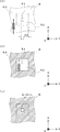
- FIG. 2 shows an inkjet coating method in which coating is performed on the substrate W using the inkjet coating apparatus of the present embodiment.
- the periphery of one hole portion H in the coating region R is shown enlarged.
- a plurality of hole portions H are formed in the coating pattern P formed on the substrate W.
- the portion to be the hole portion H is set as a non-application region R1 as shown in FIG. 2A, and no application liquid is discharged to the non-application region R1, and the outside portion of the non-application region R1 The coating liquid is discharged.
- the outer portion of the non-application area R1 is not applied at once, but first, as shown in FIG. 2A, an area that further surrounds the vicinity area R2, which is an area surrounding the non-application area R1.
- the application operation is controlled by the controller 7 so that the application liquid is applied to the peripheral region R3.
- the process of applying to the peripheral region R3 is referred to as a peripheral application step.
- the base material W on which the peripheral coating step has been performed is in a state in which a coating film is formed on the outer portion of the neighboring region R2, as shown by hatching in FIG. Then, application
- the step of applying to the vicinity region R2 is referred to as a vicinity application step.
- the application to the peripheral region R3 by the peripheral application step is performed before the application to the neighboring region R2 by the vicinity application step.
- An atmosphere of a solvent volatilized from the droplets forming the peripheral region R3 is formed in the environment, and the solvent is less likely to volatilize from the applied droplets. Therefore, even if the application is performed with fine discharge position resolution in the vicinity application step, the progress of the volatilization of the solvent from the liquid droplets that have landed on the vicinity region R2 is suppressed, and the liquid droplets are bonded with a low viscosity. Therefore, unevenness of the shape when combined is less likely to occur. As a result, as shown by hatching in FIG. 2 (c), a hole portion H with good positional accuracy and shape accuracy is formed.
- the meaning of the term “to make the discharge position resolution fine” in this description means that the coating unit 21 scans in the X-axis direction from the end to the end of the coating region (main scanning) and then moves in the Y-axis direction (sub-scanning). Although the distance is shortened and the landing position of the droplet can be set finely, the time required for coating for forming the coating pattern P becomes long.
- the inkjet coating method of the present invention is not used, and the peripheral region R3 and the neighboring region R2 are applied at a time with fine discharge position resolution in order to increase the positional accuracy of the hole portion H, the neighboring region Since the drying (solvent volatilization) proceeds from the droplets that have landed on the substrate W before the application of the coating liquid to the R2 is completed, the droplets do not normally combine on the substrate W, and the holes There is a possibility that unevenness occurs in the shape between the portions H.
- application is performed with different discharge position resolutions in the peripheral application step and the vicinity application step, and the application is performed in the vicinity application step under a condition that the discharge position resolution is finer than that in the peripheral application step.
- the application is performed with a discharge position resolution of 70.5 ⁇ m in the peripheral application step, and the discharge position resolution in the vicinity application step. Is applied at 8.8 um.
- the amount of the droplet is 42 pL, and the diameter of the droplet when landing on the substrate W is about 90 ⁇ m.
- the hole portion is compared with the case where the peripheral region R3 and the neighboring region R2 are applied at once. It is possible to improve the position accuracy and shape accuracy. In particular, the effect is large when the hole portion H has a width of 30 ⁇ m or less.
- the width d1 is shown only in the Y-axis direction, but the same can be said in the X-axis direction.
- the vicinity region R2 is preferably a region where the distance from the hole portion H (distance d2 in FIG. 2A) is 300 ⁇ m or less. By doing so, the entire vicinity region R2 is easily brought into a solvent atmosphere during the vicinity application step. Further, d2 is preferably 50 ⁇ m or more so that the liquid droplets are not ejected to the non-application region R1 even if the droplets are ejected to the vicinity region R2. In FIG. 2A, the distance d2 is shown only in the Y-axis direction, but the same can be said in the X-axis direction.
- the control unit 7 calculates the position where the hole portion H should be provided based on the distortion obtained by the distortion recognition unit 4, and applies the coating for forming the coating pattern P. Correct the position information.
- the step of recognizing the distortion of the substrate W and correcting the position to be the non-application region R1 is referred to as a position correction step.
- the application is performed with fine discharge position resolution.
- the base material W is distorted and the hole portions H are not regularly arranged
- the neighboring region R2 and the peripheral region R3 are applied together with a coarse discharge position resolution in one scan, It is possible that the nozzle 22 is not located at a place where the hole portion H can be formed with high positional accuracy.
- the application is performed with fine discharge position resolution in the vicinity region R2, the application to the vicinity region R2 is performed so that each hole portion H has high positional accuracy. Can do.
- the control unit 7 calculates the droplet discharge position in the vicinity region R2, and as a result, the non-application region is caused by the droplet discharge position resolution. It is also conceivable that the droplet discharge position relative to R1 varies for each hole H. On the other hand, in the present embodiment, even when the relative droplet discharge position with respect to the non-application region R1 varies for each hole portion H, when the plurality of hole portions H having the same size are formed, they are discharged to the neighboring region R2. The number of droplets to be made is uniform. By doing so, it becomes easy to accurately form the hole portion H of the same size.
- step S1 when the feeding device 2 and the winding device 3 are operated to transport the substrate W (step S1), the portion where the coating region R is provided is placed on the substrate holding unit 6, and the substrate The holding unit 6 sucks and holds the substrate W (step S2).
- the distortion recognition unit 4 acquires the coordinates of the alignment marks AM1 to AM4 (step S3), and the control unit 7 calculates distortion information of the substrate W (step S4).
- the application liquid is applied while the application unit 21 scans the application region R in the X-axis direction and the Y-axis direction.
- the peripheral application step is performed first, and when the nozzle 22 reaches the coordinates in the peripheral region R3 set in step S5, the droplets are discharged from the nozzle 22. (Step S6).
- a portion of the coating region R excluding the non-coating region R1 and the neighboring region R2 with respect to each hole H is defined as one peripheral region R3.
- step S7 the neighborhood application step is performed, and when the nozzle 22 reaches the coordinates in the neighborhood region R3 set in step S5, droplets are ejected from the nozzle 22 (step S7).
- step S8 After the peripheral coating step and the proximity coating step are completed and the coating pattern P is formed on the substrate W, the adsorption holding of the substrate W by the substrate holding unit 6 is released (step S8), and the next substrate W Provided for transport.
- the hole portion H is described as a contact hole, but is not limited thereto.
- the inkjet coating method of the present invention is also applied when forming a hole for connecting a jumper wiring and an ITO (Indium Tin Oxide) film in the manufacture of an NFC (Near Field Communication) substrate, a touch panel, etc. Is possible.
- a portion excluding the non-application region R1 and the neighboring region R2 for each hole H in the application region R is defined as one peripheral region R3, and a portion excluding the non-application region R1 and the neighboring region R2 in the peripheral application step. Is applied at a time, and then the application to each adjacent region R2 is performed in the vicinity application step.
- the present invention is not limited to this, and the peripheral region R3 is also divided for each hole portion H, and for each hole portion H. You may make it perform a periphery application
- the nozzles 22 are arranged in a row in the coating unit 21, but the present invention is not limited to this.
- the nozzles 22 may be arranged in a staggered manner.
- the base material W is long and is transported by a roll-to-roll method.
- the present invention is not limited to this, and the base material W is placed on the base material holding unit 6 one by one by a single wafer method. May be.
Landscapes
- Engineering & Computer Science (AREA)
- Physics & Mathematics (AREA)
- General Physics & Mathematics (AREA)
- Theoretical Computer Science (AREA)
- Manufacturing & Machinery (AREA)
- Application Of Or Painting With Fluid Materials (AREA)
- Coating Apparatus (AREA)
Abstract
微小なホール部を精度良く形成することが可能なインクジェット塗布方法およびインクジェット塗布装置を提供する。具体的には、インクジェット法により塗布液を吐出して塗布を行い、また一部非塗布領域R1を設けることにより、ホール部Hを有する塗布膜を基材W上に形成するインクジェット塗布方法であり、非塗布領域R1を囲む領域である近傍領域R2をさらに囲む領域である周辺領域R3に塗布を行う周辺塗布ステップと、近傍領域R2に塗布を行う近傍塗布ステップと、を有する。
Description
本発明は、基板上にインクジェット法により塗布膜パターンを形成するインクジェット塗布方法およびインクジェット塗布装置に関するものである。
近年液晶ディスプレイ、有機ELディスプレイなどは薄型化が進んでおり、この薄型ディスプレイに用いられる半導体装置には小型化、高密度実装が強く求められている。このような要求に対応するために、半導体装置の配線は多層化されており、絶縁膜をはさんで上下に位置する配線がこの絶縁膜の一部を貫通するコンタクトホールを介して電気的に接続される形態をとっている。
このようにコンタクトホールを有する絶縁膜を形成するにあたり、従来は特許文献1に示すようにまず塗布などにより基材全面に絶縁膜を形成した後、露光、エッチングの工程を経て、絶縁膜中にコンタクトホールを形成していた。これに対し、近年ではコンタクトホールにあたる部分を除いてインクジェット法により絶縁膜材料の塗布を行うことにより、コンタクトホールを有する絶縁膜を形成する方法が提案されている。これにより、露光、エッチングの工程を省くことができ、低コスト化、製造時間短縮が期待できる。
しかし、インクジェット法によりコンタクトホールを有する絶縁膜を形成する場合、精度良くコンタクトホールを形成することが困難であるという問題があった。具体的には、コンタクトホールは幅が20um~30um程度の微小なものであり、このコンタクトホールを精度良く形成するために吐出位置精度を細かくして塗布液の塗布を行うと、その最中に先に塗布した部分から乾燥が進行してしまっていた。その結果、塗布された液滴同士がうまく繋がらないためコンタクトホールの形状に歪みが生じ、配線間の導通不良を生じてしまうおそれがあった。
本発明は、上記問題点に鑑みてなされたものであり、微小なホール部を精度良く形成することが可能なインクジェット塗布方法およびインクジェット塗布装置を提供することを目的としている。
上記課題を解決するために本発明のインクジェット塗布方法は、インクジェット法により塗布液を吐出して塗布を行い、また一部非塗布領域を設けることにより、ホール部を有する塗布膜を基材上に形成するインクジェット塗布方法であり、前記非塗布領域を囲む領域である近傍領域をさらに囲む領域である周辺領域に塗布を行う周辺塗布ステップと、前記近傍領域に塗布を行う近傍塗布ステップと、を有することを特徴としている。
上記インクジェット塗布方法によれば、ホール部を精度良く形成することができる。具体的には、近傍塗布ステップに先立って周辺塗布ステップを行うことにより、周辺領域から揮発する溶剤の雰囲気が近傍領域上に形成されるため、近傍塗布ステップの最中における近傍領域に塗布された塗布液の乾燥が抑えられ、ホール部の形状にムラが生じにくくなる。
また、前記近傍塗布ステップでは、前記周辺塗布ステップよりも吐出位置分解能を細かくして塗布を行うと良い。
こうすることにより、吐出位置精度があまり重要でない周辺領域では時間をかけずに塗布することができ、また、精度を要するホール部は精度良く形成することが可能である。
また、前記周辺塗布ステップの前に、基材の歪みを認識して前記非塗布領域とすべき位置を補正する位置補正ステップを有すると良い。
こうすることにより、仮に基材に歪みが生じていても、必要な位置にホール部を精度良く形成することが可能である。
また、同じ大きさの前記ホール部を複数形成させるにあたり、前記近傍領域に吐出する塗布液の液滴数を均一にすると良い。
こうすることにより、同じ大きさのホール部を正確に形成しやすくなる。
また、前記ホール部の幅は30um以下であると良い。
このような微小なホール部を形成する場合であっても、本発明の塗布方法であればホール部を精度良く形成することが可能である。
また、前記近傍領域の外縁は、前記ホール部の外縁から50um以上300um以下の距離にあると良い。
こうすることにより、近傍塗布ステップの際、近傍領域上全体を溶剤雰囲気にしやすくなる。
また、上記課題を解決するために本発明のインクジェット塗布装置は、塗布液を吐出するノズルと、基材を保持する基材保持部と、前記ノズルと前記基材保持部とを前記基材保持部に保持された基材の面方向に相対移動させる駆動装置と、前記ノズルによる基材への塗布動作を制御する制御部と、を有し、インクジェット法により基材に塗布膜を形成するインクジェット塗布装置であり、前記制御部は、前記塗布膜の一部にホール部が設けられるように、前記ホール部に相当する部分である非塗布領域および当該非塗布領域を囲む領域である近傍領域を設定し、前記近傍領域をさらに囲む領域である周辺領域に塗布を行った後、前記近傍領域に塗布を行うように塗布動作を制御することを特徴としている。
上記インクジェット塗布装置によれば、ホール部を精度良く形成することができる。具体的には、周辺領域に塗布を行った後、近傍領域に塗布を行うことにより、周辺領域から揮発する溶剤の雰囲気が近傍領域上に形成されるため、近傍塗布への塗布の最中における近傍領域に塗布された塗布液の乾燥が抑えられ、ホール部の形状にムラが生じにくくなる。
本発明のインクジェット塗布方法およびインクジェット塗布装置によれば、微小なホール部を精度良く形成することが可能である。
本発明の一実施形態におけるインクジェット塗布装置を図1に示す。図1(a)は、インクジェット塗布装置1の上面図、図1(b)は、インクジェット塗布装置1の正面図である。
本実施形態のインクジェット塗布装置1は、送り出し装置2、巻き取り装置3、歪み認識部4、塗布部5、および基材保持部6を有しており、送り出し装置2から送り出され巻き取り装置3によって巻き取られる帯状の基材Wに対し、基材保持部6において固定された基材Wの塗布領域Rに対して塗布部5が塗布することにより塗布パターンPを有する塗布膜を形成するものである。また、基材保持部6に保持されている基材Wの歪みが塗布部5による処理の前に歪み認識部4によって認識され、その認識結果に基づいて、塗布部5が処理を行うべき基材W上の位置の補正が行われたのち、塗布部5による処理が行われる。
また、インクジェット塗布装置1は、コンピュータプログラムを記憶する記憶装置等を有するコンピュータからなる制御部7を備え、この制御部7により、各種計算、インクジェット塗布装置1が有する駆動機構の動作の制御などが行われる。
なお、以下の説明では、基材保持部6上で基材Wが搬送される方向をY軸方向と呼ぶ。また、水平面上でY軸方向と直交する方向をX軸方向とし、また、X軸方向およびY軸方向と直交する方向をZ軸方向とする。
基材W上には、四辺形状の塗布領域Rが帯状の基材Wの長尺方向に並んで複数形成されている。また、この帯状の基材Wはインクジェット塗布装置1による電極形成工程より後の工程で塗布領域R毎に裁断され、たとえば有機ELディスプレイの基板となる。なお、本説明では塗布領域RはX軸方向には1個のみの配列となっているが、これに限らず複数個配列されていても良い。
送り出し装置2は、帯状の基材Wが巻かれた筒状体が取り外し可能な機構を有し、また、巻き取り装置3は、基材Wを巻き取ってゆく筒状体が取り外し可能な機構を有する。これら筒状体を図示しない駆動機構により回転させることにより、基材Wは、送り出し装置2から巻き取り装置3へ送り出される。その間、塗布部5により基材Wへ塗布液の塗布が行われ、巻き取り装置3には、塗布液の塗布処理が完了した基材Wが巻き取られてゆく。
歪み認識部4は、カメラガントリ12に搭載されたカメラ11と、カメラ11をX軸方向およびY軸方向に移動させる駆動装置13とを有している。
カメラ11は、例えばCCDカメラであり、基材Wの塗布領域Rの周辺に配置されたアライメントマークAM1乃至アライメントマークAM4を撮像する。駆動装置13は、カメラガントリ12をX軸方向に移動させる機能と、カメラ11をカメラガントリ12に沿ってY軸方向に移動させる機能とを有し、例えばリニアガイドおよびモータ等によって構成される。また、認識部4の下方には、後述の基材保持部6が設けられており、この基材保持部6が基材Wを保持した状態において、アライメントマークAM1乃至アライメントマークAM4の撮像が行われる。
また、歪み認識部4は、駆動装置13およびカメラ11と関連して機能する図示しない座標取得部を備えており、この座標取得部は、カメラ11が撮像した画像を処理する機能を有するほか、駆動装置13によって移動したカメラ11のX軸方向およびY軸方向の位置(座標)を制御(管理)する。このため、カメラ11によって取得された画像に基づいて、座標取得部はアライメントマークAM1乃至アライメントマークAM4の座標を取得することができる。なお、座標取得部の機能は、制御部7のコンピュータプログラムが実行されることで発揮される。
また、歪み認識部4は、座標取得部が得たアライメントマークAM1乃至アライメントマークAM4の座標情報をもとに、塗布領域Rの歪み情報(塗布領域Rがどのような形状に歪んでいるのか)を算出する歪み情報算出部を備え、この歪み情報算出部が算出した歪み情報をもとに、後述の通り塗布部5が処理を行うべき基材W上の位置情報の補正が行われる。なお、歪み情報算出部の機能は、制御部7のコンピュータプログラムが実行されることで発揮される。
塗布部5は、基材Wの塗布領域R上にたとえば絶縁膜材料を塗布することにより、基材W上に塗布パターンPを有する塗布膜を形成する。塗布パターンPには複数の微小なホール部Hが設けられており、このホール部はたとえばコンタクトホールの役割を果たし、このコンタクトホールには後の工程で導電材料が充填され、塗布膜の上下に設けられる配線パターン同士を導通させる。
塗布部5は、塗布ユニット21と、塗布ガントリ23と、塗布ユニット21をX軸方向およびY軸方向に移動させる駆動装置とを有している。なお、本実施形態では、塗布ユニット21を移動させる駆動装置はカメラ11を移動させる駆動装置13と同一であり、駆動装置13はカメラ11と独立して塗布ユニット21を移動させる。また、塗布ガントリ23には、基材保持部6の基材載置面と直交する方向(Z軸方向)に回転軸を有する回転手段24が取付けられ、この回転手段24の回転軸に塗布ユニット21が取付けられており、塗布ユニット21はこの回転軸を中心に回動することが可能である。なお、本実施形態では、この回転手段24も、駆動装置13により駆動される。
塗布ユニット21には、塗布領域Rに対して塗布液を吐出する吐出ノズル22が一方向に等間隔で複数並んで設けられており、塗布ユニット21が回転手段24によって回動することにより、吐出ノズル22の配列方向を変化させることが可能である。このように吐出ノズル22の配列方向を変化させることにより、吐出ノズル22のY軸方向の間隔を調節することが可能である。
塗布部5による塗布動作では、塗布ユニット21がX軸方向に走査(主走査)する際に、それぞれの吐出ノズル22が吐出目標とする塗布領域R上の所定位置の上方に差し掛かったときに塗布液を吐出する。この動作を塗布ユニット21のY軸方向の移動(副走査)を挟んで連続して行うことにより、塗布領域R上に塗布パターンPを形成することが可能である。なお、吐出ノズル22が塗布領域R上の所定位置の上方に差し掛かるタイミングは、それぞれの所定位置の座標と、それぞれの吐出ノズル22の位置とを制御部7が管理しておくことにより、算出することが可能である。
また、塗布部5は、基材保持部6に保持された基材Wの塗布領域Rに対して、塗布ユニット21の吐出ノズル22から塗布液を吐出させて塗布する各種動作の制御を行う塗布動作制御部を備えている。また、塗布動作制御部は、各吐出ノズル22のX軸方向およびY軸方向の位置(座標)を制御(管理)することができる。この塗布動作制御部の機能は、制御部7のコンピュータプログラムが実行されることで発揮される。
基材保持部6は、平坦面である基材載置面を有し、基材載置面上で帯状の基材Wの一部を水平に保持する。このように保持された基材Wに対して塗布部5が処理を行う。また、基材載置面には多数の吸引孔が設けられており、この吸引孔と図示しない真空ポンプが接続され、真空ポンプが作動することにより、基材載置面上で基材Wを吸着固定することができる。
制御部7は、CPUおよびRAMやROMを有するコンピュータであり、上記の通り座標取得部、歪み情報算出部、塗布動作制御部の機能を有して歪み認識部4、塗布部5の動作の制御を行うほか、送り出し装置2、巻き取り装置3の回転速度を制御することにより基材Wの搬送の制御も行う。
また、制御部7は、歪み認識部4によって得られた歪みに基づいて、基材W上へ塗布パターンPを形成するための位置情報を補正計算する処理位置補正部の機能も有している。
また、制御部7は、ハードディスクや、RAMまたはROMなどのメモリからなる、各種情報を記憶する記憶装置を有しており、基材Wに塗布部5が塗布パターンPを形成するための位置情報がこの記憶装置に記憶される。また、この記憶装置には、上記処理位置補正部の機能により補正された塗布位置情報も一時的に記憶され、この記憶されたデータをもとに塗布部5を動作させることができる。
次に、本実施形態のインクジェット塗布装置を用いて基材Wへ塗布を行うインクジェット塗布方法について、図2に示す。この図2では塗布領域R内の1つのホール部Hの周辺が拡大して示されている。
本発明のインクジェット塗布方法では、基材Wに形成される塗布パターンPには複数のホール部Hが形成されている。このホール部Hとなる部分は図2(a)に示すように非塗布領域R1と設定され、この非塗布領域R1へは塗布液の吐出は行われず、非塗布領域R1の外側部分に対して塗布液の吐出が行われる。
ここで、本発明では、非塗布領域R1の外側部分が一度に塗布されるのではなく、まずは図2(a)の通り非塗布領域R1を囲む領域である近傍領域R2をさらに囲む領域である周辺領域R3に対して塗布液の塗布が行われるよう、制御部7により塗布動作が制御される。なお、本説明では、周辺領域R3に塗布を行う工程を周辺塗布ステップと呼ぶ。
周辺塗布ステップが行われた基材Wは、図2(b)にハッチングで示すように近傍領域R2の外側部分に塗布膜が形成された状態となる。その後、図2(b)に示す通り近傍領域R2に対して塗布が行われる。なお、本説明では、近傍領域R2に塗布を行う工程を近傍塗布ステップと呼ぶ。
ここで、塗布動作により基材Wに着弾した塗布液の液滴からは溶剤の揮発が進行する。特に液滴の周囲の環境が乾燥しているほど溶剤の揮発はすぐに開始し、また揮発の進行速度が速くなる。
一方、本発明のインクジェット塗布方法では近傍塗布ステップによる近傍領域R2への塗布の前に周辺塗布ステップによる周辺領域R3への塗布が行われているため、近傍塗布ステップが行われる時には近傍領域R2上には周辺領域R3を形成した液滴から揮発した溶剤の雰囲気が形成されており、塗布された液滴から溶剤が揮発しにくい環境となっている。そのため、近傍塗布ステップでは吐出位置分解能を細かくして塗布を行ったとしても、近傍領域R2に着弾した液滴からの溶剤の揮発の進行は抑えられ、液滴同士が粘度が低めの状態で結合できるため、結合したときの形状のムラが生じにくくなる。その結果、図2(c)にハッチングで示すように位置精度および形状の精度が良いホール部Hが形成される。
ここで、本説明における吐出位置分解能を細かくするという文言の意味は、塗布ユニット21が塗布領域の端から端までX軸方向に走査(主走査)した後にY軸方向に移動(副走査)する距離を短くすることであり、液滴の着弾位置を細かく設定することができる反面、塗布パターンPを形成するための塗布に要する時間が長くなる。そのため、仮に本発明のインクジェット塗布方法を使用せず、また、ホール部Hの位置精度を高くするために吐出位置分解能を細かくして周辺領域R3および近傍領域R2を一度に塗布する場合、近傍領域R2への塗布液の塗布が完了する前に先に基材Wに着弾した液滴から乾燥(溶剤の揮発)が進行するため、基材W上で液滴同士が正常に結合せず、ホール部H間で形状にムラが生じるおそれがある。
また、本実施形態では、周辺塗布ステップと近傍塗布ステップにおいて異なる吐出位置分解能で塗布が行われ、近傍塗布ステップでは周辺塗布ステップよりも吐出位置分解能が細かい条件で塗布が行われている。具体的には、Y軸方向に近接するノズル22間の距離が70.5umの条件において、周辺塗布ステップでは吐出位置分解能は70.5umで塗布が行われ、また、近傍塗布ステップでは吐出位置分解能は8.8umで塗布が行われている。なお、液滴の量は42pLであり、基材Wに着弾したときの液滴の径は約90umである。
こうすることにより、吐出位置精度があまり重要でない周辺領域R3には時間をかけずに塗布することができ、また、精度を要するホール部Hは精度良く形成することが可能である。すなわち、品質の良い塗布パターンPを製造時間を短くして形成させることが可能である。
なお、ノズル22から1回の動作で吐出される液滴の量が14pLの場合もあり、このとき基材Wに着弾したときの液滴の径は約50umである。この場合、液滴量が42pLの場合と比べて液滴径が小さくなるのにあわせて、周辺塗布ステップにおける吐出位置分解能も35.25umと小さく設定されている。
また、本発明のインクジェット塗布方法では、形成するホール部Hの幅(図2(a)における幅d1)が小さいほど、周辺領域R3および近傍領域R2を一度に塗布する場合と比較してホール部の位置精度および形状精度を高めることができる。特にホール部Hが30um以下の幅である場合にその効果は大きい。なお、図2(a)ではY軸方向のみ幅d1を記載しているが、X軸方向においても同様のことが言える。
また、近傍領域R2は、ホール部Hからの距離(図2(a)における距離d2)が300um以下となる領域であると良い。こうすることにより、近傍塗布ステップの際、近傍領域R2上全体を溶剤雰囲気にしやすくなる。また、近傍領域R2に液滴を吐出しても非塗布領域R1にはみ出ることがないよう、d2は50um以上であると良い。なお、図2(a)ではY軸方向のみ距離d2を記載しているが、X軸方向においても同様のことが言える。
なお、本発明のインクジェット塗布方法では、近傍塗布ステップ中、周辺領域R3を形成した液滴から揮発した溶剤により近傍領域R2上が溶剤雰囲気となっている必要があるため、周辺塗布ステップ完了後近傍塗布ステップを開始するまでに長い時間をかけることなく、周辺領域R3において液滴が含む溶剤の揮発が進行している間に近傍塗布ステップが行われることが望ましい。
ここで、複数のホール部Hの中で近接する2つのホール部Hがある場合は、これを考慮し、それぞれのホール部Hを囲む2つの近傍領域R2が構成できるように、上記d2の寸法範囲内において小さめの寸法で設定される。
また、本実施形態では、基材保持部6が基材Wを保持した後、周辺塗布ステップを行う前に歪み認識部4が基材Wの歪みを認識する工程を有している。これは、基材Wがたとえば樹脂フィルムなど可撓性を有するものであった場合、塗布部5による塗布工程よりも前の工程において熱処理などが施されていると基材Wに歪みが生じているおそれがあるためである。この場合、ホール部Hを設けるべき位置も変化するため、制御部7は歪み認識部4によって得られた歪みに基づいてホール部Hを設けるべき位置を算出し、塗布パターンP形成のための塗布位置情報を補正する。なお、本説明では、基材Wの歪みを認識して非塗布領域R1とすべき位置を補正する工程を位置補正ステップと呼ぶ。
このように位置補正ステップを設けることにより、仮に基材に歪みが生じていても、必要な位置にホール部を精度良く形成することが可能である。
また、本発明では少なくとも近傍領域R2では吐出位置分解能を細かくして塗布を行っている。ここで、基材Wに歪みがあってホール部Hが規則通りに配列されていない場合、1回のスキャンで近傍領域R2と周辺領域R3とを粗い吐出位置分解能で一緒に塗布する場合にはホール部Hを位置精度良く形成できる場所にノズル22が位置していないこともあり得る。これに対し、本発明の塗布方法では、近傍領域R2では吐出位置分解能を細かくして塗布を行っているため、それぞれのホール部Hが位置精度良くなるように近傍領域R2への塗布を行うことができる。
また、同じ大きさのホール部Hを形成する場合であっても、近傍領域R2における液滴の吐出位置を制御部7が計算した結果、液滴の吐出位置分解能に起因して、非塗布領域R1に対する相対的な液滴吐出位置がホール部Hごとにばらつくことも考えられる。これに対し本実施形態では、たとえ非塗布領域R1に対する相対的な液滴吐出位置がホール部Hごとにばらついたとしても、同じ大きさのホール部Hを複数形成させるにあたり、近傍領域R2に吐出する液滴数は均一にしている。こうすることにより、同じ大きさのホール部Hを正確に形成しやすくなる。
次に、本実施形態におけるインクジェット塗布装置1の動作フローを図3に示す。
まず、送り出し装置2および巻き取り装置3が動作して基材Wが搬送されることにより(ステップS1)、塗布領域Rが設けられた部分が基材保持部6上に載置され、基材保持部6が基材Wを吸着保持する(ステップS2)。
次に、歪み認識部4がアライメントマークAM1乃至アライメントマークAM4の座標を取得し(ステップS3)、制御部7は基材Wの歪み情報を算出する(ステップS4)。
次に、この基材Wの歪み情報を反映し、制御部7は塗布位置情報を補正する(ステップS5)。具体的には、各ホール部Hを形成する非塗布領域R1の位置を算出し、各ホール部Hに対応する近傍領域R2を設定し、各近傍領域R2および周辺領域R3において液滴を吐出する座標を設定する。そして、制御部7内に既存の(歪みが無い場合の)データをこれら設定された座標データへ一時的に置き換える。なお、これらステップS3からステップS5までの動作が、本説明における位置補正ステップに相当する。
次に、塗布領域R上を塗布ユニット21がX軸方向およびY軸方向に走査しながら塗布液の塗布が行われる。制御部7による塗布動作の制御により、先に周辺塗布ステップが実施され、ステップS5において設定した周辺領域R3内の座標にノズル22が到達した際に、そのノズル22から液滴の吐出が行われる(ステップS6)。なお、本実施形態では、塗布領域Rにおいて各ホール部Hに対する非塗布領域R1および近傍領域R2を除く部分を1つの周辺領域R3としている。
次に近傍塗布ステップが実施され、ステップS5において設定した近傍領域R3内の座標にノズル22が到達した際に、そのノズル22から液滴の吐出が行われる(ステップS7)。
周辺塗布ステップおよび近傍塗布ステップが完了して基材Wに塗布パターンPが形成された後、基材保持部6による基材Wの吸着保持が解除され(ステップS8)、次の基材Wの搬送に備えられる。
以上のインクジェット塗布方法およびインクジェット塗布装置により、微小なホール部を精度良く形成することが可能である。
なお、上記の説明では、ホール部Hはコンタクトホールであると記載しているが、これに限らない。たとえば、NFC(Near Field Communication、近距離無線通信)基板、タッチパネルなどの製造におけるジャンパ配線とITO(Indium Tin Oxide)膜との接続用の穴を形成する際も、本発明のインクジェット塗布方法を適用することが可能である。
また、本実施形態では、塗布領域Rにおいて各ホール部Hに対する非塗布領域R1および近傍領域R2を除く部分を1つの周辺領域R3とし、周辺塗布ステップにおいて非塗布領域R1および近傍領域R2を除く部分を一度に塗布し、その後に近傍塗布ステップにおいて各近傍領域R2への塗布を行う形態をとっているが、これに限らず、周辺領域R3もホール部Hごとに区分けし、ホール部Hごとに順番に周辺塗布ステップと近傍塗布ステップとを行うようにしても良い。
また、図1では塗布ユニット21にノズル22は一列に配列されているが、これに限らない。たとえば、ノズル22が千鳥状に配置されていても構わない。
また、本実施形態は基材Wは長尺でありロールトゥロール方式で搬送される形態をとっているが、これに限らず、枚葉方式で1枚ずつ基材保持部6に載置されても良い。
1 インクジェット塗布装置
2 送り出し装置
3 巻き取り装置
4 歪み認識部
5 塗布部
6 基材保持部
7 制御部
11 カメラ
12 カメラガントリ
13 駆動装置
21 塗布ユニット
22 吐出ノズル
23 塗布ガントリ
24 回転手段
AM1~AM4 アライメントマーク
H ホール部
P 塗布パターン
R 塗布領域
W 基材
2 送り出し装置
3 巻き取り装置
4 歪み認識部
5 塗布部
6 基材保持部
7 制御部
11 カメラ
12 カメラガントリ
13 駆動装置
21 塗布ユニット
22 吐出ノズル
23 塗布ガントリ
24 回転手段
AM1~AM4 アライメントマーク
H ホール部
P 塗布パターン
R 塗布領域
W 基材
Claims (7)
- インクジェット法により塗布液を吐出して塗布を行い、また一部非塗布領域を設けることにより、ホール部を有する塗布膜を基材上に形成するインクジェット塗布方法であり、
前記非塗布領域を囲む領域である近傍領域をさらに囲む領域である周辺領域に塗布を行う周辺塗布ステップと、
前記近傍領域に塗布を行う近傍塗布ステップと、
を有することを特徴とする、インクジェット塗布方法。 - 前記近傍塗布ステップでは、前記周辺塗布ステップよりも吐出位置分解能を細かくして塗布を行うことを特徴とする、請求項1に記載のインクジェット塗布方法。
- 前記周辺塗布ステップの前に、基材の歪みを認識して前記非塗布領域とすべき位置を補正する位置補正ステップを有することを特徴とする、請求項1または2のいずれかに記載のインクジェット塗布方法。
- 同じ大きさの前記ホール部を複数形成させるにあたり、前記近傍領域に吐出する塗布液の液滴数を均一にすることを特徴とする、請求項1から3のいずれかに記載のインクジェット塗布方法。
- 前記ホール部の幅は30um以下であることを特徴とする、請求項1から4のいずれかに記載のインクジェット塗布方法。
- 前記近傍領域の外縁は、前記ホール部の外縁から50um以上300um以下の距離にあることを特徴とする、請求項1から5のいずれかに記載のインクジェット塗布方法。
- 塗布液を吐出するノズルと、
基材を保持する基材保持部と、
前記ノズルと前記基材保持部とを前記基材保持部に保持された基材の面方向に相対移動させる駆動装置と、
前記ノズルによる基材への塗布動作を制御する制御部と、
を有し、インクジェット法により基材に塗布膜を形成するインクジェット塗布装置であり、
前記制御部は、前記塗布膜の一部にホール部が設けられるように、前記ホール部に相当する部分である非塗布領域および当該非塗布領域を囲む領域である近傍領域を設定し、前記近傍領域をさらに囲む領域である周辺領域に塗布を行った後、前記近傍領域に塗布を行うように塗布動作を制御することを特徴とする、インクジェット塗布装置。
Applications Claiming Priority (2)
| Application Number | Priority Date | Filing Date | Title |
|---|---|---|---|
| JP2015-025054 | 2015-02-12 | ||
| JP2015025054A JP2016147223A (ja) | 2015-02-12 | 2015-02-12 | インクジェット塗布方法およびインクジェット塗布装置 |
Publications (1)
| Publication Number | Publication Date |
|---|---|
| WO2016129443A1 true WO2016129443A1 (ja) | 2016-08-18 |
Family
ID=56615573
Family Applications (1)
| Application Number | Title | Priority Date | Filing Date |
|---|---|---|---|
| PCT/JP2016/052984 Ceased WO2016129443A1 (ja) | 2015-02-12 | 2016-02-02 | インクジェット塗布方法およびインクジェット塗布装置 |
Country Status (2)
| Country | Link |
|---|---|
| JP (1) | JP2016147223A (ja) |
| WO (1) | WO2016129443A1 (ja) |
Cited By (1)
| Publication number | Priority date | Publication date | Assignee | Title |
|---|---|---|---|---|
| WO2017090547A1 (ja) * | 2015-11-26 | 2017-06-01 | 東レエンジニアリング株式会社 | 膜パターン描画方法、塗布膜基材、及び、塗布装置 |
Citations (5)
| Publication number | Priority date | Publication date | Assignee | Title |
|---|---|---|---|---|
| JP2003282561A (ja) * | 2002-03-26 | 2003-10-03 | Seiko Epson Corp | デバイスの製造方法及びデバイス製造装置 |
| JP2005199227A (ja) * | 2004-01-19 | 2005-07-28 | Seiko Epson Corp | 描画方法、描画装置、デバイス及び電子機器 |
| JP2006003870A (ja) * | 2004-05-19 | 2006-01-05 | Seiko Epson Corp | カラーフィルタ基板の製造方法、電気光学装置の製造方法、電気光学装置、電子機器 |
| JP2006216477A (ja) * | 2005-02-07 | 2006-08-17 | Seiko Epson Corp | 有機el装置、有機el装置の製造方法、電子機器 |
| JP2014008481A (ja) * | 2012-07-02 | 2014-01-20 | Seiko Epson Corp | 液滴吐出方法 |
-
2015
- 2015-02-12 JP JP2015025054A patent/JP2016147223A/ja active Pending
-
2016
- 2016-02-02 WO PCT/JP2016/052984 patent/WO2016129443A1/ja not_active Ceased
Patent Citations (5)
| Publication number | Priority date | Publication date | Assignee | Title |
|---|---|---|---|---|
| JP2003282561A (ja) * | 2002-03-26 | 2003-10-03 | Seiko Epson Corp | デバイスの製造方法及びデバイス製造装置 |
| JP2005199227A (ja) * | 2004-01-19 | 2005-07-28 | Seiko Epson Corp | 描画方法、描画装置、デバイス及び電子機器 |
| JP2006003870A (ja) * | 2004-05-19 | 2006-01-05 | Seiko Epson Corp | カラーフィルタ基板の製造方法、電気光学装置の製造方法、電気光学装置、電子機器 |
| JP2006216477A (ja) * | 2005-02-07 | 2006-08-17 | Seiko Epson Corp | 有機el装置、有機el装置の製造方法、電子機器 |
| JP2014008481A (ja) * | 2012-07-02 | 2014-01-20 | Seiko Epson Corp | 液滴吐出方法 |
Cited By (1)
| Publication number | Priority date | Publication date | Assignee | Title |
|---|---|---|---|---|
| WO2017090547A1 (ja) * | 2015-11-26 | 2017-06-01 | 東レエンジニアリング株式会社 | 膜パターン描画方法、塗布膜基材、及び、塗布装置 |
Also Published As
| Publication number | Publication date |
|---|---|
| JP2016147223A (ja) | 2016-08-18 |
Similar Documents
| Publication | Publication Date | Title |
|---|---|---|
| JP5587616B2 (ja) | インクジェット塗布装置及び方法 | |
| KR101454106B1 (ko) | 전기 수력학을 이용한 패턴라인 형성장치 및 패턴라인을 형성하는 방법 | |
| JP5693943B2 (ja) | 配向膜形成液の塗布装置および配向膜形成基板の製造方法 | |
| JP2010017683A (ja) | 液滴塗布装置及び液滴塗布方法 | |
| WO2016129443A1 (ja) | インクジェット塗布方法およびインクジェット塗布装置 | |
| CN108511634A (zh) | 喷墨打印机及其打印方法 | |
| JP5869927B2 (ja) | 塗布装置および塗布方法 | |
| WO2018034031A1 (ja) | 凹版、印刷装置、印刷方法およびパターン担持体 | |
| US10932372B2 (en) | Fluid discharge device | |
| JP2018086637A (ja) | 絶縁膜材料の塗布方法 | |
| JP2018122254A (ja) | 塗布装置、および塗布方法 | |
| JP2011249195A (ja) | 印刷装置 | |
| CN110181934B (zh) | 一种印刷装置、印刷系统及其印刷方法 | |
| JP6805018B2 (ja) | 塗布装置、および塗布方法 | |
| JP6420608B2 (ja) | 基材処理方法および基材処理装置 | |
| JP2006239976A (ja) | パターン形成装置、位置補正方法 | |
| JP4604533B2 (ja) | 座標精度確認方法、および電気光学装置の製造方法 | |
| JP2018126717A (ja) | 塗布装置、および塗布方法 | |
| JP2007090191A (ja) | インキ吐出印刷装置 | |
| JP4534546B2 (ja) | 液滴吐出装置、位置調整方法、電気光学装置の製造方法 | |
| JP2006032905A (ja) | 薬液塗布装置及び薬液塗布方法 | |
| JP6532778B2 (ja) | 液滴吐出装置、液滴吐出方法、プログラム及びコンピュータ記憶媒体 | |
| JP2019209672A (ja) | インクジェット装置、およびそれを用いた機能素子の製造方法 | |
| JP2019018534A (ja) | 印刷装置および印刷方法 | |
| JP2009247948A (ja) | 液滴吐出装置、機能液の着弾位置補正方法、電気光学装置の製造方法および電気光学装置 |
Legal Events
| Date | Code | Title | Description |
|---|---|---|---|
| 121 | Ep: the epo has been informed by wipo that ep was designated in this application |
Ref document number: 16749087 Country of ref document: EP Kind code of ref document: A1 |
|
| NENP | Non-entry into the national phase |
Ref country code: DE |
|
| 122 | Ep: pct application non-entry in european phase |
Ref document number: 16749087 Country of ref document: EP Kind code of ref document: A1 |