WO2016125835A1 - 樹脂膜形成用複合シート、及び樹脂膜付きチップの製造方法 - Google Patents
樹脂膜形成用複合シート、及び樹脂膜付きチップの製造方法 Download PDFInfo
- Publication number
- WO2016125835A1 WO2016125835A1 PCT/JP2016/053259 JP2016053259W WO2016125835A1 WO 2016125835 A1 WO2016125835 A1 WO 2016125835A1 JP 2016053259 W JP2016053259 W JP 2016053259W WO 2016125835 A1 WO2016125835 A1 WO 2016125835A1
- Authority
- WO
- WIPO (PCT)
- Prior art keywords
- resin film
- film
- forming
- resin
- sheet
- Prior art date
- Legal status (The legal status is an assumption and is not a legal conclusion. Google has not performed a legal analysis and makes no representation as to the accuracy of the status listed.)
- Ceased
Links
Images

Classifications
-
- H—ELECTRICITY
- H10—SEMICONDUCTOR DEVICES; ELECTRIC SOLID-STATE DEVICES NOT OTHERWISE PROVIDED FOR
- H10W—GENERIC PACKAGES, INTERCONNECTIONS, CONNECTORS OR OTHER CONSTRUCTIONAL DETAILS OF DEVICES COVERED BY CLASS H10
- H10W72/00—Interconnections or connectors in packages
- H10W72/071—Connecting or disconnecting
-
- B—PERFORMING OPERATIONS; TRANSPORTING
- B32—LAYERED PRODUCTS
- B32B—LAYERED PRODUCTS, i.e. PRODUCTS BUILT-UP OF STRATA OF FLAT OR NON-FLAT, e.g. CELLULAR OR HONEYCOMB, FORM
- B32B27/00—Layered products comprising a layer of synthetic resin
-
- B—PERFORMING OPERATIONS; TRANSPORTING
- B32—LAYERED PRODUCTS
- B32B—LAYERED PRODUCTS, i.e. PRODUCTS BUILT-UP OF STRATA OF FLAT OR NON-FLAT, e.g. CELLULAR OR HONEYCOMB, FORM
- B32B7/00—Layered products characterised by the relation between layers; Layered products characterised by the relative orientation of features between layers, or by the relative values of a measurable parameter between layers, i.e. products comprising layers having different physical, chemical or physicochemical properties; Layered products characterised by the interconnection of layers
- B32B7/04—Interconnection of layers
- B32B7/12—Interconnection of layers using interposed adhesives or interposed materials with bonding properties
-
- C—CHEMISTRY; METALLURGY
- C09—DYES; PAINTS; POLISHES; NATURAL RESINS; ADHESIVES; COMPOSITIONS NOT OTHERWISE PROVIDED FOR; APPLICATIONS OF MATERIALS NOT OTHERWISE PROVIDED FOR
- C09D—COATING COMPOSITIONS, e.g. PAINTS, VARNISHES OR LACQUERS; FILLING PASTES; CHEMICAL PAINT OR INK REMOVERS; INKS; CORRECTING FLUIDS; WOODSTAINS; PASTES OR SOLIDS FOR COLOURING OR PRINTING; USE OF MATERIALS THEREFOR
- C09D201/00—Coating compositions based on unspecified macromolecular compounds
-
- C—CHEMISTRY; METALLURGY
- C09—DYES; PAINTS; POLISHES; NATURAL RESINS; ADHESIVES; COMPOSITIONS NOT OTHERWISE PROVIDED FOR; APPLICATIONS OF MATERIALS NOT OTHERWISE PROVIDED FOR
- C09D—COATING COMPOSITIONS, e.g. PAINTS, VARNISHES OR LACQUERS; FILLING PASTES; CHEMICAL PAINT OR INK REMOVERS; INKS; CORRECTING FLUIDS; WOODSTAINS; PASTES OR SOLIDS FOR COLOURING OR PRINTING; USE OF MATERIALS THEREFOR
- C09D7/00—Features of coating compositions, not provided for in group C09D5/00; Processes for incorporating ingredients in coating compositions
- C09D7/40—Additives
-
- C—CHEMISTRY; METALLURGY
- C09—DYES; PAINTS; POLISHES; NATURAL RESINS; ADHESIVES; COMPOSITIONS NOT OTHERWISE PROVIDED FOR; APPLICATIONS OF MATERIALS NOT OTHERWISE PROVIDED FOR
- C09J—ADHESIVES; NON-MECHANICAL ASPECTS OF ADHESIVE PROCESSES IN GENERAL; ADHESIVE PROCESSES NOT PROVIDED FOR ELSEWHERE; USE OF MATERIALS AS ADHESIVES
- C09J201/00—Adhesives based on unspecified macromolecular compounds
-
- C—CHEMISTRY; METALLURGY
- C09—DYES; PAINTS; POLISHES; NATURAL RESINS; ADHESIVES; COMPOSITIONS NOT OTHERWISE PROVIDED FOR; APPLICATIONS OF MATERIALS NOT OTHERWISE PROVIDED FOR
- C09J—ADHESIVES; NON-MECHANICAL ASPECTS OF ADHESIVE PROCESSES IN GENERAL; ADHESIVE PROCESSES NOT PROVIDED FOR ELSEWHERE; USE OF MATERIALS AS ADHESIVES
- C09J7/00—Adhesives in the form of films or foils
- C09J7/20—Adhesives in the form of films or foils characterised by their carriers
Definitions
- the present invention relates to a composite sheet for forming a resin film and a method for manufacturing a chip with a resin film using the composite sheet for forming a resin film.
- a semiconductor chip (hereinafter simply referred to as “chip”) having electrodes such as bumps is mounted on the circuit surface of the semiconductor chip, and the chip electrodes are bonded to the substrate. For this reason, the surface of the chip opposite to the side bonded to the substrate (hereinafter also referred to as “the back surface of the chip”) may be exposed.
- a resin film made of an organic material is formed on the exposed back surface of the chip and may be taken into the semiconductor device as a chip with a resin film.
- the resin film functions as a protective film for preventing the occurrence of cracks after the dicing process and packaging, and for bonding the obtained chip onto another member such as a die pad part or another semiconductor chip.
- the function as an adhesive film can also be imparted.
- this chip with a resin film is formed by applying a solution of a resin-containing composition to the back surface of a wafer by spin coating or the like to form a coating film, and then drying and curing the coating film. And the resultant wafer with resin film is diced.
- a wafer with a resin film and a chip with a resin film can also be manufactured.
- Various films for forming a resin film have been proposed as a material for forming a resin film on the back surface of the chip or the back surface of the wafer.
- Patent Document 1 includes two energy ray-curable protective film forming layers containing a polymer component made of an acrylic copolymer, an energy ray-curable component, a dye or pigment, an inorganic filler, and a photopolymerization initiator.
- a film for protecting a chip having a configuration sandwiched between release sheets is disclosed.
- the chip protection film can form a protective film with good laser marking recognizability, hardness, and adhesion to the wafer by irradiation with energy rays. The process can be simplified as compared with conventional film for chip protection.
- Patent Document 2 discloses a dicing tape having a dicing tape having a pressure-sensitive adhesive layer on a substrate, and a wafer back surface protective film that is colored and has a predetermined elastic modulus on the pressure-sensitive adhesive layer of the dicing tape.
- An integrated wafer back surface protective film is disclosed. According to the description in Patent Document 2, the wafer back surface protective film is said to have a good holding force with the semiconductor wafer in the dicing process of the semiconductor wafer.
- the protective film described in Patent Documents 1 and 2 is attached to the wafer, the protective film to be attached on the wafer is displaced, or foreign matter is adhered to the wafer. It may happen that the protective film is stuck so as to be included. In such a case, the protective film may be desired to be reworked (reattached) from the wafer. However, it is often difficult to cleanly rework the protective film once pasted on the wafer without causing a residue on the wafer.
- the protective films disclosed in Patent Documents 1 and 2 are intended to improve the adhesion to the wafer at the time of sticking and the holding power to the wafer after the sticking. In this case, it is very difficult to rework due to high adhesion to the wafer.
- Patent Documents 1 and 2 the protective film described has been studied from the viewpoint of adhesion to the wafer at the time of application and holding power to the wafer after application, but once applied to the wafer. No consideration has been given to the reworkability of the film.
- the present invention provides a composite sheet for forming a resin film that has excellent reworkability and can be peeled even after being attached to a silicon wafer, and a method for manufacturing a chip with a resin film using the composite sheet for forming a resin film. Objective.
- a composite sheet for forming a resin film which has a configuration in which a film for forming a resin film capable of forming a resin film is directly laminated on a support sheet and satisfies the following requirements (I) and (II).
- the peel force ( ⁇ 1) required to peel the resin film-forming film from the silicon wafer measured under the peel condition (x) in (1) is 0.05 to 10.0 N / 25 mm.
- the force ( ⁇ 1) is a value equal to or greater than the peel force ( ⁇ 1).
- the peeling force ( ⁇ 2) required for peeling the support sheet is 0.02 to 5.0 N / 25 mm.
- the support sheet is an adhesive sheet having an adhesive layer on a substrate, The composite for forming a resin film according to any one of the above [1] to [3], wherein the adhesive layer of the pressure-sensitive adhesive sheet and the surface ( ⁇ ) of the film for forming a resin film are directly laminated. Sheet.
- the composite sheet for forming a resin film of the present invention is excellent in reworkability and can be peeled even after being attached to a silicon wafer, and the peeled silicon wafer can be reused. Therefore, according to the manufacturing method of the chip
- (meth) acrylate is used as a term indicating both “acrylate” and “methacrylate”, and the same applies to other similar terms.
- the “energy beam” refers to, for example, ultraviolet rays or electron beams, and ultraviolet rays are preferable.
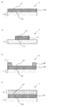
- FIG. 1 is a cross-sectional view of a composite sheet for forming a resin film of one embodiment of the present invention.
- the resin film-forming composite sheet of the present invention (hereinafter also simply referred to as “composite sheet”) is directly laminated with a resin film-forming film capable of forming a resin layer on the support sheet. It has a configuration.
- composite sheet the resin film-forming composite sheet of the present invention
- forms such as a long tape shape and a single-leaf label, may be sufficient.
- a composite sheet 1a having a configuration in which a resin film forming film 20 is directly laminated on the surface of a support sheet 10 as shown in FIG.
- the shape of the resin film-forming film 20 of the composite sheet of one embodiment of the present invention is preferably substantially the same shape as the silicon wafer that is the adherend or a shape that can include the shape of the silicon wafer.
- the support sheet 10 and the resin film-forming film 20 have substantially the same shape, but as shown in FIG. 1B, the resin film-forming film.
- the composite sheet 1b having a shape 20 smaller than the shape of the support sheet 10 may be used.
- a composite sheet 1c having a ring-shaped jig adhesive layer 40 can be cited.
- the ring-shaped jig adhesive layer 40 is provided for the purpose of improving the adhesive strength to a jig such as a ring frame, and has a base material (core material). Or it can form from an adhesive.
- the jig adhesive layer 40 is provided on the surface ( ⁇ ) 21 of the resin film-forming film 20, but the composite according to one aspect of the present invention.
- seat it is good also as a structure which provided the jig
- the exposed surface ( ⁇ ) 21 of the resin film forming film 20 included in the composite sheet 1a shown in FIG. 1A serves as a bonding surface with a silicon wafer as an adherend. Therefore, in order to prevent foreign matter from attaching to the surface ( ⁇ ) 21 or being damaged, as shown in FIG. 1 (d), the surface ( ⁇ ) 21 of the resin film forming film 20 is further formed on the silicon wafer. It is good also as the composite sheet 1d which laminated
- the composite sheet 1d shown in FIG. 1 (d) shows a configuration in which a carrier sheet 50 is provided on the surface ( ⁇ ) 21 of the resin film forming film 20 included in the composite sheet 1a shown in FIG. 1 (a).
- the carrier sheet 50 is provided to prevent dirt and the like from adhering to the surface ( ⁇ ) 21 of the resin film-forming film 20 during storage, and is used when the composite sheet 1d is attached to a silicon wafer. Is to be removed.
- the carrier sheet 50 which the composite sheet 1d shown in FIG.1 (d) has is comprised from base materials for carrier sheets, such as a resin film
- the base material for carrier sheets, such as the said resin film is mentioned. It is preferable that the sheet has a surface subjected to a peeling treatment.
- the carrier sheet may be further provided so as to cover the surface ( ⁇ ) 21 and the surface of the support sheet 10 in the composite sheet 1b of FIG.
- the carrier sheet may be provided so as to cover the surface ( ⁇ ) 21 and the surface of the jig bonding layer 40.
- the support sheet included in the composite sheet of one embodiment of the present invention may be a sheet composed only of a base material, or may be a pressure-sensitive adhesive sheet having a pressure-sensitive adhesive layer on the base material.
- an adhesive sheet when using an adhesive sheet as a support sheet, it becomes the structure which the adhesive layer of the said adhesive sheet and the surface ((beta)) 22 of the film 20 for resin film formation laminated
- the support sheet used in one embodiment of the present invention may be a sheet composed of a base material having a surface subjected to a peeling treatment.
- a composite sheet using a sheet composed of a substrate having a surface that has been subjected to a release treatment includes a surface that has been subjected to a release treatment of the substrate, and a surface ( ⁇ ) 22 of the resin film-forming film 20. It becomes the structure which laminated
- the composite sheet for forming a resin film of the present invention is required to satisfy the following requirements (I) and (II).
- the peel force ( ⁇ 1) required to peel the resin film-forming film from the silicon wafer measured under the peel condition (x) in (1) is 0.05 to 10.0 N / 25 mm.
- the force ( ⁇ 1) is a value equal to or greater than the peel force ( ⁇ 1).
- peeling force ( ⁇ 1)” and “peeling force ( ⁇ 1)” defined in the above requirements (I) and (II) are values measured by the conditions and methods described in the examples. means.
- FIG. 2 is a cross-sectional view illustrating a configuration when the composite sheet for forming a resin film of one embodiment of the present invention is attached to a silicon wafer.
- the “peeling force ( ⁇ 1)” defined in the requirement (I) is the relationship between the silicon wafer 100 and the surface ( ⁇ ) 21 of the resin film forming film 20 on the side to be bonded to the silicon wafer. It defines the peeling force at the boundary surface ⁇ 1.
- the peel force ( ⁇ 1) needs to be 0.05 to 10.0 N / 25 mm.
- the conventional film for forming a resin film as disclosed in Patent Documents 1 and 2 is often intended to improve adhesion and retention with a silicon wafer, and the above peeling force ( ⁇ 1) Material design has been made to increase the value.
- the peeling force ( ⁇ 1) exceeds 10.0 N / 25 mm, it is practically difficult to rework the resin film-forming film once pasted on the silicon wafer. That is, in such a case, if the resin film forming film stuck on the silicon wafer is forcibly removed, a part of the resin film forming film remains on the silicon wafer or the silicon wafer is damaged. The silicon wafer cannot be reused.
- the above peeling force ( ⁇ 1) is adjusted to 10.0 N / 25 mm or less. Yes.
- the above-mentioned peeling force ( ⁇ 1) is less than 0.05 N / 25 mm, it tends to be liable to be lifted or peeled particularly at the end of the composite sheet after being attached to the silicon wafer.
- the peel force ( ⁇ 1) is preferably 0.06 to 9.5 N / 25 mm, more preferably 0.07 to 9.2 N / 25 mm, and more preferably 0.1 to 9.0 N / 25 mm, more preferably 0.2 to 8.0 N / 25 mm, still more preferably 0.5 to 6.0 N / 25 mm, still more preferably 0.5 to 4.0 N / 25 mm, particularly preferably 0. .5 to 3.0 N / 25 mm.
- the method for adjusting the peel force ( ⁇ 1) includes, for example, the types and contents of polymer components, curable components, inorganic fillers, additives, and the like contained in the resin film-forming film.
- a method of appropriately selecting and adjusting the amount can be mentioned.
- “Peeling force ( ⁇ 1)” defined in requirement (II) is, for example, as shown in FIG. 2, the surface ( ⁇ ) 22 of the resin film-forming film 20 on the side directly laminated with the support sheet 10 The peeling force at the boundary surface ⁇ 1 with the support sheet 10 is defined.
- the “peeling force ( ⁇ 1)” is the boundary surface between the surface ( ⁇ ) of the resin film-forming film and the adhesive layer of the adhesive sheet used as the support sheet. The peel force is specified.
- the peel force ( ⁇ 1) needs to be a value equal to or greater than the peel force ( ⁇ 1).
- the peeling force ( ⁇ 1) is less than the peeling force ( ⁇ 1), all or part of the resin film-forming film remains on the silicon wafer when the composite sheet attached to the silicon wafer is reworked. Therefore, the silicon wafer cannot be reused.
- the difference between the peel force ( ⁇ 1) and the peel force ( ⁇ 1) [( ⁇ 1) ⁇ ( ⁇ 1)] is preferably 0.01 N / 25 mm or more, more preferably It is 0.1 N / 25 mm or more, more preferably 0.15 N / 25 mm or more, still more preferably 0.2 N / 25 mm or more, still more preferably 0.5 N / 25 mm or more, and particularly preferably 1.0 N / 25 mm or more.
- the difference [ ⁇ 1 ⁇ 1] between the peel force ( ⁇ 1) and the peel force ( ⁇ 1) is preferably 20 N / 25 mm or less, more preferably 12 N / 25 mm or less.
- the peel force ( ⁇ 1) is preferably 0.05 to 20.0 N / 25 mm, more preferably 0.2 to 18.0 N / 25 mm, and still more preferably 0.5 to 16.0 N. / 25 mm, more preferably 1.0 to 14.0 N / 25 mm.
- the peel force ( ⁇ 1) is 0.05 N / 25 mm or more, the phenomenon that the resin film forming film and the support sheet are separated at the boundary surface ⁇ 1 when the composite sheet attached to the silicon wafer is reworked. Can be prevented.
- the peeling force ( ⁇ 1) is 20.0 N / 25 mm or less, the pick-up property can be improved when picking up the diced silicon wafer.
- examples of the method for adjusting the peeling force ( ⁇ 1) include, for example, the types and contents of the above-described components contained in the resin film-forming film, and the types of support sheets used (base materials and And a method of appropriately selecting and adjusting the type of resin film, the type and blending amount of the resin and additive constituting the release layer, and the type and blending amount of the resin and additive constituting the pressure-sensitive adhesive layer).
- the concrete adjustment method of peeling force ((beta) 1) it can adjust by considering suitably the matter described in the item of each component mentioned later.
- the composite sheet of one embodiment of the present invention preferably further satisfies the following requirement (III).
- the peeling force ( ⁇ 2) required for peeling the support sheet is 0.02 to 5.0 N / 25 mm.
- peeling force ( ⁇ 2)” defined in the above requirement (III) means a value measured by the conditions and methods described in the examples.
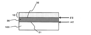
- FIG. 3 is a cross-sectional view illustrating a structure when a resin film is formed over a silicon wafer using the composite sheet for forming a resin film of one embodiment of the present invention.
- the “peeling force ( ⁇ 2)” defined in the requirement (III) is, for example, as shown in FIG. 3 between the surface ( ⁇ ′) 32 of the resin film 30 formed from the resin film forming film and the support sheet 10. This defines the peeling force at the boundary surface ⁇ 2.
- the “peeling force ( ⁇ 2)” is the peeling force at the interface between the surface of the resin film ( ⁇ ′) and the pressure-sensitive adhesive layer of the pressure-sensitive adhesive sheet used as the support sheet. It becomes the thing which stipulated.
- the peeling force ( ⁇ 2) is 0.02 N / 25 mm or more, there is a certain holding force with respect to the chip when picking up the diced silicon wafer to obtain the chip. The phenomenon of being scattered can be suppressed.
- the peel force ( ⁇ 2) is 5.0 N / 25 mm or less, the pick-up property can be improved when picking up the diced silicon wafer.
- the peeling force ( ⁇ 2) is preferably from 0.03 to 4.0 N / 25 mm, more preferably from 0.05 to 2.5 N / 25 mm, and still more preferably from the above viewpoint. It is 10 to 2.0 N / 25 mm, more preferably 0.15 to 1.5 N / 25 mm.
- the peeling force (at the boundary surface ⁇ 2 between the silicon wafer 100 and the surface ( ⁇ ′) 31 on the side of the resin film 30 formed from the resin film-forming film laminated with the silicon wafer ( ⁇ 2) is not particularly limited, but is preferably at least a value larger than the above-described peeling force ( ⁇ 1) and peeling force ( ⁇ 2).
- the method for adjusting the peel force ( ⁇ 2) is not particularly limited, and examples thereof include the same preparation method as the above-described peel force ( ⁇ 1).
- the adhesive sheet which has an adhesive layer formed from the adhesive composition containing energy-beam curable resin. By irradiating energy rays, the adhesive force of the pressure-sensitive adhesive layer is reduced, and the peeling force ( ⁇ 2) can be easily adjusted to belong to the above range.
- each layer constituting the composite sheet for resin film formation each layer constituting the composite sheet for forming a resin film of one embodiment of the present invention will be described.
- the film for forming a resin film included in the composite sheet of one embodiment of the present invention may be any film as long as the peel strengths ( ⁇ 1) and ( ⁇ 1) fall within the above range, but the polymer component (A) and the curable component ( It is preferable that it is a film for resin film formation containing B).
- the said film for resin film formation is further with an inorganic filler (C), a coloring agent (D), and a coupling agent (E) with a component (A) and (B).
- one or more selected from general-purpose additives (F) the components (A) to (F) contained in the resin film-forming film will be described.
- the value of peeling force ((alpha) 1), ((beta) 1), and ((beta) 2) can be adjusted by considering suitably combining the following suitable matters in each component.
- the “polymer component” means a compound having a mass average molecular weight (Mw) of 20,000 or more and having at least one repeating unit.
- Mw mass average molecular weight
- the resin film-forming film used in one embodiment of the present invention can impart flexibility and film-forming properties, and can improve sheet property maintainability.
- the mass average molecular weight (Mw) of the polymer component (A) is preferably 20,000 or more, more preferably 20,000 to 3,000,000, more preferably 50,000 to 2,000,000, still more preferably 100,000 to 1.5 million.
- the value of the mass average molecular weight (Mw) of the polymer component or the like is a value in terms of standard polystyrene measured by a gel permeation chromatography (GPC) method, and is specifically carried out. It is the value measured based on the method described in the examples.
- the content of the polymer component (A) is preferably 5 to 50% by mass, more preferably 8 to 40% by mass, and further preferably 10 to 10% by mass with respect to the total mass (100% by mass) of the resin film-forming film. It is 35% by mass, more preferably 15-30% by mass.
- the above-mentioned “content of component (A) relative to the total mass (100% by mass) of the resin film-forming film” is “a composition that is a material for forming a resin film-forming film” It is synonymous with "content of a component (A) with respect to the total mass (100 mass%) of an active ingredient in”, and it is the same also about content of the other component demonstrated below. That is, in the definition of the content of each component, the term “relative to the total mass (100% by mass) of the resin film-forming film” means “the active ingredient of the composition that is a material for forming the resin film-forming film” May be replaced with the term “with respect to the total mass (100% by mass)”. Furthermore, the above “active ingredient” means a component excluding substances that do not directly or indirectly affect the physical properties of the formed sheet, such as a solvent in the composition, specifically, , Means components other than solvents such as water and organic solvents contained in the composition.
- the polymer component (A) preferably contains an acrylic polymer (A1), but other than the acrylic polymer (A1), polyester, phenoxy resin, polycarbonate, polyether, polyurethane, polysiloxane, rubber-based A non-acrylic polymer (A2) such as a polymer may be contained. These polymer components may be used alone or in combination of two or more.
- the content of the acrylic polymer (A1) with respect to the total mass (100% by mass) of the polymer component (A) contained in the resin film-forming film used in one embodiment of the present invention is preferably 50 to 100. % By mass, more preferably 60 to 100% by mass, still more preferably 70 to 100% by mass, and still more preferably 80 to 100% by mass.
- the weight average molecular weight (Mw) of the acrylic polymer (A1) is preferably 20,000 to 3,000,000, more preferably 100,000 to 150, from the viewpoint of imparting flexibility and film-forming property to the resin film-forming film. It is 10,000, more preferably 150,000 to 1,200,000, still more preferably 250,000 to 1,000,000.
- the glass transition temperature (Tg) of the acrylic polymer (A1) is preferably ⁇ 40 ° C. or higher, more preferably ⁇ from the viewpoint of adjusting the peeling forces ( ⁇ 1), ( ⁇ 1), and ( ⁇ 2) to the above range. 20 to 50 ° C., more preferably ⁇ 10 to 30 ° C., still more preferably 0 to 20 ° C.
- the value of the glass transition temperature of the acrylic polymer (Tg) of absolute temperature calculated by the following formula (1) (unit: K) a glass transition temperature represented by (Tg K) It is a value converted to Celsius temperature (unit: ° C.).
- W 1, W 2, W 3, W 4 ⁇ shows the mass fraction of the monomer components constituting the resin component (mass%), Tg 1, Tg 2 , Tg 3 , Tg 4 ... Indicate the glass transition temperature (unit: K) of the homopolymer of each monomer component constituting the resin component.
- acrylic polymer (A1) examples include polymers having an alkyl (meth) acrylate as a main component. Specifically, a configuration derived from an alkyl (meth) acrylate having an alkyl group having 1 to 18 carbon atoms.
- An acrylic polymer having the unit (a1) is preferable, and from the viewpoint of adjusting the peel strengths ( ⁇ 1), ( ⁇ 1), and ( ⁇ 2) to the above ranges, other than the structural unit (a1) and the structural unit (a1)
- An acrylic copolymer having other structural unit (a2) is more preferred.
- the acrylic polymer (A1) may be used alone or in combination of two or more.
- the form of the copolymer may be any of a block copolymer, a random copolymer, an alternating copolymer, and a graft copolymer. Good.
- the number of carbon atoms of the alkyl group of the alkyl (meth) acrylate constituting the structural unit (a1) is preferably 1 to 18, more preferably from the viewpoint of imparting flexibility and film forming property to the resin film-forming film. Is from 1 to 12, more preferably from 1 to 8.
- alkyl (meth) acrylate examples include methyl (meth) acrylate, ethyl (meth) acrylate, propyl (meth) acrylate, butyl (meth) acrylate, pentyl (meth) acrylate, 2-ethylhexyl (meth) acrylate, and isooctyl ( Examples include meth) acrylate, n-octyl (meth) acrylate, n-nonyl (meth) acrylate, isononyl (meth) acrylate, decyl (meth) acrylate, lauryl (meth) acrylate, stearyl (meth) acrylate, and the like. In addition, you may use these alkyl (meth) acrylates individually or in combination of 2 or more types.
- an alkyl (meth) acrylate having an alkyl group having 1 to 3 carbon atoms is preferable, and methyl (meth) acrylate is more preferable.
- the content of the structural unit (a1-1) derived from the alkyl (meth) acrylate having an alkyl group having 1 to 3 carbon atoms in the acrylic polymer (A1) is the total structural unit of the acrylic polymer (A1). It is preferably 5 to 98% by mass, more preferably 10 to 95% by mass, and still more preferably 20 to 90% by mass with respect to (100% by mass).
- the acrylic polymer (A1) used in one embodiment of the present invention is an alkyl having 1 to 3 carbon atoms.
- a copolymer having both the derived structural unit (a1-2) is preferable.
- the content ratio [(a1-1) / (a1-2)] of the structural unit (a1-1) to the structural unit (a1-2) is preferably 1/99 to 99/1, more preferably 10 / 90 to 90/10, more preferably 15/85 to 85/15.
- the content of the structural unit (a1) in the acrylic polymer (A1) is preferably 50 to 100% by weight, more preferably based on the total structural unit (100% by weight) of the acrylic polymer (A1). 60 to 99% by mass, more preferably 70 to 95% by mass.
- the acrylic polymer (A1) may have a structural unit (a2) derived from another monomer other than the structural unit (a1) as long as the effects of the present invention are not impaired.
- the monomer constituting the structural unit (a2) include functional group-containing monomers having functional groups such as hydroxy group-containing monomers, carboxy group-containing monomers, and epoxy group-containing monomers; vinyl esters such as vinyl acetate and vinyl propionate.
- Olefin monomers such as ethylene, propylene and isobutylene
- Aromatic vinyl monomers such as styrene, methylstyrene and vinyltoluene
- Diene monomers such as butadiene and isoprene
- Nitrile monomers such as (meth) acrylonitrile and the like.
- hydroxy-containing monomer examples include 2-hydroxyethyl (meth) acrylate, 2-hydroxypropyl (meth) acrylate, 3-hydroxypropyl (meth) acrylate, 2-hydroxybutyl (meth) acrylate, and 3-hydroxybutyl (meth) )
- hydroxyalkyl (meth) acrylates such as 4-hydroxybutyl (meth) acrylate; and unsaturated alcohols such as vinyl alcohol and allyl alcohol.
- 2-hydroxyethyl (meth) acrylate is preferable.
- carboxy group-containing monomer examples include (meth) acrylic acid, maleic acid, fumaric acid, itaconic acid and the like.
- epoxy group-containing monomer examples include glycidyl (meth) acrylate, ⁇ -methylglycidyl (meth) acrylate, (3,4-epoxycyclohexyl) methyl (meth) acrylate, and 3-epoxycyclo-2-hydroxypropyl (meth).
- epoxy group-containing (meth) acrylic acid esters such as acrylate; non-acrylic epoxy group-containing monomers such as glycidyl crotonate and allyl glycidyl ether; and the like.
- An acrylic polymer having a structural unit derived from an epoxy group-containing monomer and having an Mw of 20,000 or more has thermosetting properties, but is not a curable component (B) but a polymer component (A). It shall be included in the concept of
- the acrylic polymer (A1) used in one embodiment of the present invention contains a hydroxy group and a structural unit (a1).
- a copolymer having a structural unit (a2-1) derived from a monomer is preferable.
- the content of the structural unit (a2-1) derived from the hydroxy group-containing monomer in the acrylic polymer (A1) is preferably based on the total structural unit (100% by mass) of the acrylic polymer (A1).
- the amount is 1 to 40% by mass, more preferably 2 to 30% by mass, and still more preferably 5 to 25% by mass.
- the acrylic polymer (A1) used in one embodiment of the present invention has a structural unit (a1) and a structural unit derived from a nitrile monomer (a1).
- a copolymer having a2-2) is preferred.
- the content of the structural unit (a2-2) derived from the nitrile monomer in the acrylic polymer (A1) is preferably 1 with respect to the total structural units (100% by mass) of the acrylic polymer (A1). It is ⁇ 40 mass%, more preferably 2 to 35 mass%, still more preferably 5 to 30 mass%.
- the content of the structural unit derived from the epoxy group-containing monomer in the acrylic polymer (A1) is increased, the adhesion between the obtained resin film-forming film and the silicon wafer is improved, and the value of the peeling force ( ⁇ 1) Tend to rise. Therefore, in one aspect of the present invention, the smaller the content of the structural unit derived from the epoxy group-containing monomer in the acrylic polymer (A1), the better.
- the content of the structural unit derived from the epoxy group-containing monomer in the acrylic polymer (A1) is preferably 0 to 4 mass with respect to the total structural units (100 mass%) of the acrylic polymer (A1). %, More preferably 0 to 3% by mass, still more preferably 0 to 2% by mass, and still more preferably 0% by mass.
- an acrylic polymer (A1) The content of the structural unit derived from the carboxyl group-containing monomer is preferably as small as possible.
- an epoxy thermosetting component is used as the curable component (B)
- the content of the structural unit derived from the carboxy group-containing monomer is based on the total structural unit (100% by mass) of the acrylic polymer (A1).
- the content is preferably 0 to 10% by mass, more preferably 0 to 5% by mass, still more preferably 0 to 2% by mass, and still more preferably 0% by mass.
- the content of the structural unit (a2) in the acrylic polymer (A1) is preferably 1 to 40% by weight, more preferably based on the total structural unit (100% by weight) of the acrylic polymer (A1). It is 2 to 35% by mass, more preferably 5 to 30% by mass.
- Non-acrylic polymer (A2) The resin film-forming film used in the present invention may contain a non-acrylic polymer (A2) as a polymer component having an Mw of 20,000 or more other than the above-mentioned acrylic polymer (A1), if necessary.
- the non-acrylic polymer (A2) include polyester, phenoxy resin, polycarbonate, polyether, polyurethane, polysiloxane, rubber polymer, and the like. These non-acrylic polymers (A2) may be used alone or in combination of two or more.
- a phenoxy resin having an epoxy group with Mw of 20,000 or more has thermosetting properties, but is not included in the curable component (B) but in the non-acrylic polymer (A2).
- the mass average molecular weight (Mw) of the non-acrylic polymer (A2) is preferably 20,000 or more, more preferably 20,000 to 100,000, still more preferably 20,000 to 80,000.
- the curable component (B) plays a role of curing a resin film-forming film to form a hard resin film.
- the resin film-forming film used in the present invention preferably contains at least one of a thermosetting component (B1) and an energy ray-curable component (B2) as the curable component (B). It is more preferable that the thermosetting component (B1) is included from the viewpoint of suppressing coloring of the formed resin film, from the viewpoint of sufficiently proceeding the curing reaction, and from the viewpoint of cost reduction.
- a thermosetting component (B1) it is preferable to contain the compound which has a functional group which reacts at least by heating, and it is more preferable to contain the compound (B11) which has an epoxy group.
- an energy-beam curable component (B2) it is preferable to contain the compound (B21) which has a polymerizable functional group which reacts by energy beam irradiation. Curing is realized by the functional groups of these curable components reacting to form a three-dimensional network structure.
- thermosetting component (B1)) As the thermosetting component (B1), an epoxy thermosetting component is preferable.
- the epoxy thermosetting component it is preferable to use a combination of a thermosetting agent (B12) together with a compound (B11) having an epoxy group.
- the compound (B11) and the thermosetting agent (B12) having an epoxy group are compounds having a mass average molecular weight (Mw) of less than 20,000, and are distinguished from the polymer component (A) described above. .
- a compound having an epoxy group having a mass average molecular weight (Mw) of 20,000 or more and a thermosetting agent are included in the polymer component (A).
- epoxy compound (B11) examples include polyfunctional epoxy resins, bisphenol A diglycidyl ether and hydrogenated products thereof, orthocresol novolac epoxy resins, and the like.
- examples include novolak type epoxy resins, dicyclopentadiene type epoxy resins, biphenyl type epoxy resins, bisphenol A type epoxy resins, bisphenol F type epoxy resins, phenylene skeleton type epoxy resins, and other epoxy compounds having two or more functional groups. These epoxy compounds (B11) may be used alone or in combination of two or more.
- the mass average molecular weight (Mw) of the epoxy compound (B11) is less than 20,000, but it is used in combination with the component (A) to suppress the viscosity of the composition forming the resin film-forming film and handle it. From the standpoint of improving the properties, etc., it is preferably 10,000 or less, and more preferably 100 to 10,000.
- the composition that is a material for forming the resin film-forming film is a liquid epoxy compound and a solid epoxy at 25 ° C. as an epoxy compound (B11). It is preferable that it contains a compound together.
- the ratio is preferably 5/95 to 95/5, more preferably 10/90 to 90/10, still more preferably 20/80 to 80/20, and still more preferably 30/70 to 70/30.
- the value of the peel force ( ⁇ 1) increases as the proportion of the liquid epoxy compound increases, and the value of the peel force ( ⁇ 1) tends to decrease as the proportion of the solid epoxy compound increases.
- the content of the epoxy compound (B11) is preferably 1 to 500 parts by weight, more preferably 3 to 300 parts by weight, still more preferably 10 to 150 parts by weight, even more preferably 100 parts by weight of the component (A). Is 20 to 120 parts by mass.
- thermosetting agent (B12) functions as a curing agent for the epoxy compound (B11).
- a thermosetting agent the compound which has 2 or more of functional groups which can react with an epoxy group in 1 molecule is preferable.
- the functional group include phenolic hydroxyl groups, alcoholic hydroxyl groups, amino groups, carboxyl groups, and acid anhydrides. Among these, a phenolic hydroxyl group, an amino group, or an acid anhydride is preferable, a phenolic hydroxyl group and an amino group are more preferable, and an amino group is still more preferable.
- thermosetting agent having a phenol group examples include polyfunctional phenol resins, biphenol resins, novolac-type phenol resins, dicyclopentadiene-type phenol resins, zyloc-type phenol resins, and aralkyl-type phenol resins.
- phenol-based thermosetting agent having an amino group examples include dicyandiamide (DICY). These thermosetting agents (B12) may be used alone or in combination of two or more.
- thermosetting agent (B12) is preferably 0.1 to 500 parts by mass, more preferably 1 to 200 parts by mass with respect to 100 parts by mass of the epoxy compound (B11).
- a curing accelerator (B13) In order to adjust the speed of thermal curing of the resin film-forming film, a curing accelerator (B13) may be used.
- the curing accelerator (B13) is preferably used in combination with the epoxy compound (B11) as the thermosetting component (B1).
- Examples of the curing accelerator (B13) include tertiary amines such as triethylenediamine, benzyldimethylamine, triethanolamine, dimethylaminoethanol, and tris (dimethylaminomethyl) phenol; 2-methylimidazole, 2-phenylimidazole, Imidazoles such as 2-phenyl-4-methylimidazole, 2-phenyl-4,5-dihydroxymethylimidazole, 2-phenyl-4-methyl-5-hydroxymethylimidazole; tributylphosphine, diphenylphosphine, triphenylphosphine Organic phosphines; tetraphenyl boron salts such as tetraphenylphosphonium tetraphenylborate and triphenylphosphine tetraphenylborate. These curing accelerators (B13) may be used alone or in combination of two or more.
- the content of the curing accelerator (B13) is The amount is preferably 0.01 to 10 parts by weight, more preferably 0.1 to 6 parts by weight, still more preferably 0.3 to 0.3 parts by weight based on 100 parts by weight of the total amount of the epoxy compound (B11) and the thermosetting agent (B12). 4 parts by mass.
- the compound (B21) having a polymerizable functional group that reacts by irradiation with energy rays may be used alone, but together with the compound (B21), a photopolymerization initiator (B22) is used. It is preferable to use in combination.
- Compound (B21) having a functional group that reacts upon irradiation with energy rays As a compound (B21) having a polymerizable functional group that reacts upon irradiation with energy rays (hereinafter also referred to as “energy ray-reactive compound (B21)”), a polymerizable functional group such as a (meth) acryloyl group or a vinyl group is used.
- trimethylolpropane tri (meth) acrylate pentaerythritol tri (meth) acrylate, pentaerythritol tetra (meth) acrylate, dipentaerythritol monohydroxypenta (meth) acrylate, dipentaerythritol hexa ( (Meth) acrylate, 1,4-butylene glycol di (meth) acrylate, 1,6-hexanediol di (meth) acrylate, oligoester (meth) acrylate, urethane (meth) acrylate oligomer, epoxy (meth) acrylate Relate, polyether (meth) acrylate, itaconic acid oligomer and the like.
- the energy beam reactive compounds (B21) may be used alone or in combination of two or more.
- the energy ray reactive compound (B21) is a compound having a mass average molecular weight (Mw) of less than 20,000, and is distinguished from the above polymer component (A).
- the energy ray-reactive compound having a mass average molecular weight (Mw) of 20,000 or more is included in the polymer component (A).
- the mass average molecular weight (Mw) of the energy ray reactive compound (B21) is less than 20,000, preferably 100 to 15,000, more preferably 300 to 10,000.
- the content of the energy ray-reactive compound (B21) is preferably 1 to 1500 parts by mass, more preferably 3 to 1200 parts by mass with respect to 100 parts by mass of the component (A).
- photopolymerization initiator (B22) examples include benzoin compounds, acetophenone compounds, acylphosphine oxide compounds, titanocene compounds, thioxanthone compounds, peroxide compounds, and the like. More specific photopolymerization initiators include, for example, 1-hydroxycyclohexyl phenyl ketone, benzoin, benzoin methyl ether, benzoin ethyl ether, benzoin isopropyl ether, benzyldiphenyl sulfide, tetramethylthiuram monosulfide, azobisisobutyronitrile.
- Photopolymerization initiators may be used alone or in combination of two or more.
- the content of the photopolymerization initiator (B22) is sufficiently advanced with respect to 100 parts by mass of the energy ray-reactive compound (B21) from the viewpoint of sufficiently proceeding the curing reaction of the resin film-forming film and suppressing the formation of residues.
- the amount is preferably 0.1 to 10 parts by mass, more preferably 1 to 5 parts by mass.
- the content of the curable component (B) is preferably 5 to 50% by mass, more preferably 8 to 40% by mass, and further preferably 10 to 10% by mass with respect to the total mass (100% by mass) of the resin film-forming film. 30% by mass, and more preferably 12-25% by mass.
- hardenable component (B) the above-mentioned epoxy compound (B11), a thermosetting component (B1) containing a thermosetting agent (B12), and a hardening accelerator (B13), and an energy beam It is total content of the energy-beam curable component (B2) containing a reactive compound (B21) and a photoinitiator (B22).
- the film for forming a resin film used in one embodiment of the present invention preferably further contains an inorganic filler (C).
- an inorganic filler (C) By including the inorganic filler (C), it becomes possible to adjust the thermal expansion coefficient of the resin film formed from the resin film forming film to an appropriate range, and to optimize the thermal expansion coefficient of the chip with the resin film. Thus, the reliability of the semiconductor device in which the chip is incorporated can be improved. Moreover, it becomes possible to reduce the moisture absorption rate of the resin film formed from the resin film forming film.
- Examples of the inorganic filler (C) include silica, alumina, talc, calcium carbonate, titanium oxide, iron oxide, silicon carbide, boron nitride and other powders, beads formed by spheroidizing them, single crystal fibers, glass fibers, and the like. Can be mentioned. These inorganic fillers (C) may be used alone or in combination of two or more. Among these, silica and alumina are preferable.
- the average particle size of the inorganic filler (C) is preferably 0.01 to 50 ⁇ m, more preferably 0.05 to 30 ⁇ m, and still more preferably 0.1 to 10 ⁇ m.
- the average particle diameter of the inorganic filler (C) is a value measured using a laser diffraction / scattering particle size distribution measuring device, and means a volume-median particle diameter (D 50 ).
- the content of the inorganic filler (C) is preferably 15 to 80% by mass, more preferably 20 to 75% by mass, and further preferably 30 to 30% by mass with respect to the total mass (100% by mass) of the resin film-forming film. It is 70% by mass, still more preferably 40 to 65% by mass, particularly preferably 45 to 60% by mass.
- the resin film-forming film used in one embodiment of the present invention preferably further contains a colorant (D).
- a colorant (D) By containing the colorant (D) in the resin film-forming film, when a semiconductor chip having a resin film formed from the resin film-forming film is incorporated in a device, infrared rays generated from surrounding devices are shielded. Thus, malfunction of the semiconductor chip can be prevented.
- colorant (D) organic or inorganic pigments and dyes can be used.
- the dye for example, any dye such as an acid dye, a reactive dye, a direct dye, a disperse dye, and a cationic dye can be used. Moreover, it does not restrict
- black pigments are preferable from the viewpoints of good shielding properties against electromagnetic waves and infrared rays, and further improving the discriminability by the laser marking method. Examples of the black pigment include carbon black, iron oxide, manganese dioxide, aniline black, activated carbon, and the like. From the viewpoint of improving the reliability of the semiconductor chip, carbon black is preferable. In addition, you may use these colorants (D) individually or in combination of 2 or more types.
- the content of the colorant (D) is preferably 0.01 to 30% by mass, more preferably 0.05 to 25% by mass, and still more preferably based on the total mass (100% by mass) of the resin film-forming film. Is 0.1 to 15% by mass, more preferably 0.15 to 5% by mass.
- the film for forming a resin film used in one embodiment of the present invention preferably further contains a coupling agent (E).
- the resin film formed from the obtained resin film-forming film can also improve water resistance without impairing heat resistance.
- the compound which reacts with the functional group which a component (A) or a component (B) has is preferable, and a silane coupling agent is more preferable.
- the silane coupling agent include ⁇ -glycidoxypropyltrimethoxysilane, ⁇ -glycidoxypropylmethyldiethoxysilane, ⁇ - (3,4-epoxycyclohexyl) ethyltrimethoxysilane, ⁇ - (methacryloxy).
- an oligomer type coupling agent is preferable.
- the molecular weight of the coupling agent (E) including the oligomer type coupling agent is preferably 100 to 15000, more preferably 150 to 10,000, more preferably 200 to 5000, still more preferably 250 to 3000, and still more preferably. Is 350-2000.
- a coupling agent (E) it is optionally included in the polymer component (A) in the resin film-forming film, the surface of the silicon wafer that is the adherend, and the resin film-forming sheet. It is considered that the value of the peeling force ( ⁇ 1) also increases in order to bond with the surface of the inorganic filler (C) to improve adhesion and cohesion. Therefore, the content of the coupling agent (E) is small from the viewpoint of adjusting the peeling forces ( ⁇ 1), ( ⁇ 1), and ( ⁇ 2) to the above range, particularly from the viewpoint of adjusting the peeling force ( ⁇ 1). Is preferred.
- the content of the coupling agent (E) is preferably 0.01 to 4% by mass, more preferably 0.05 to 2% with respect to the total mass (100% by mass) of the resin film-forming film. % By mass, more preferably 0.10 to 1.5% by mass, and still more preferably 0.15 to 1% by mass.
- the film for forming a resin film used in one embodiment of the present invention may contain a general-purpose additive (F) as necessary, in addition to the above components, within a range not impairing the effects of the present invention.
- the general-purpose additive (F) include a crosslinking agent, a leveling agent, a plasticizer, an antistatic agent, an antioxidant, an ion scavenger, a gettering agent, and a chain transfer agent.
- the content of each of these general-purpose additives (F) is preferably 0 to 10% by mass, more preferably 0 to 5% by mass with respect to the total mass (100% by mass) of the resin film-forming film.
- the content is preferably 0 to 2% by mass.
- ⁇ Method for producing resin film-forming film> There is no restriction
- the organic solvent used for preparing the resin film-forming composition solution examples include toluene, ethyl acetate, methyl ethyl ketone, and the like.
- the solid content concentration of the resin film-forming composition solution is preferably 10 to 80% by mass, more preferably 20 to 70% by mass, and still more preferably 30 to 65% by mass.
- the coating method include spin coating, spray coating, bar coating, knife coating, roll coating, roll knife coating, blade coating, die coating, and gravure coating.
- the resin film-forming film may be a single layer or a multilayer structure of two or more layers.
- a coating film was formed by applying a solution of the resin film forming composition on two or more support sheets.
- a film for forming a resin film having a multilayer structure can be produced by stacking each coating film to form a coating film and then drying the film.
- the thickness of the resin film-forming film included in the composite sheet of one embodiment of the present invention is appropriately set depending on the application, but is preferably 3 to 300 ⁇ m, more preferably 5 to 250 ⁇ m, and still more preferably 7 to 200 ⁇ m. Even when the resin film-forming film has a multilayer structure, the total thickness is preferably within the above range.
- Examples of the support sheet used in one embodiment of the present invention include a sheet composed only of a base material and a pressure-sensitive adhesive sheet having a pressure-sensitive adhesive layer on the base material.
- the composite sheet of one embodiment of the present invention has a support sheet for protecting the surface of the resin film forming sheet by a peeling sheet that prevents adhesion of dust or the like to the surface of the resin film forming sheet, or a dicing process or the like. It plays the role of a dicing sheet or the like.
- the thickness of the support sheet is appropriately selected depending on the application, but is preferably 10 to 500 ⁇ m, more preferably from the viewpoint of imparting sufficient flexibility to the composite sheet and improving the adhesiveness to the silicon wafer. Is 20 to 350 ⁇ m, more preferably 30 to 200 ⁇ m. Note that the thickness of the support sheet includes not only the thickness of the substrate constituting the support sheet but also the thickness of those layers and films when having an adhesive layer.
- a resin film As a base material which comprises a support sheet, a resin film is preferable.
- the resin film include polyethylene films such as low density polyethylene (LDPE) films and linear low density polyethylene (LLDPE) films, ethylene / propylene copolymer films, polypropylene films, polybutene films, polybutadiene films, and polymethylpentene.
- the base material used in one embodiment of the present invention may be a single layer film made of one kind of resin film or a laminated film in which two or more kinds of resin films are laminated.
- a surface-treated sheet may be used as a support sheet on the surface of a substrate such as the above-described resin film.
- these resin films may be crosslinked films. Moreover, what colored these resin films, or what gave printing etc. can be used. Furthermore, the resin film may be a sheet formed by extrusion forming a thermoplastic resin, or may be a stretched sheet, and a sheet formed by thinning and curing a curable resin by a predetermined means. May be used.
- a base material including a polypropylene film is preferable from the viewpoint that it has excellent heat resistance and has an appropriate flexibility so that it has expandability and pickup property is easily maintained.
- the single layer structure which consists only of a polypropylene film may be sufficient, and the multilayer structure which consists of a polypropylene film and another resin film may be sufficient.
- the resin film-forming film is thermosetting, the resin film constituting the base material has heat resistance, so that damage to the base material due to heat can be suppressed, and occurrence of defects in the semiconductor device manufacturing process can be suppressed.
- the peeling force ( ⁇ 1) is adjusted to the above range as the surface tension of the surface of the base material that contacts the surface ( ⁇ ) of the resin film-forming film. From this viewpoint, it is preferably 20 to 50 mN / m, more preferably 23 to 45 mN / m, still more preferably 25 to 40 mN / m.
- the thickness of the base material constituting the support sheet is preferably 10 to 500 ⁇ m, more preferably 15 to 300 ⁇ m, and still more preferably 20 to 200 ⁇ m.
- Examples of the pressure-sensitive adhesive sheet used as a support sheet in one embodiment of the present invention include those having a pressure-sensitive adhesive layer formed from a pressure-sensitive adhesive on a substrate such as the above-described resin film.
- Examples of the pressure-sensitive adhesive that is a material for forming the pressure-sensitive adhesive layer include a pressure-sensitive adhesive composition containing a pressure-sensitive adhesive resin, and the pressure-sensitive adhesive composition further contains general-purpose additives such as the above-described crosslinking agent and tackifier. May be.
- the adhesive resin when attention is paid to the structure of the resin, for example, acrylic resin, urethane resin, rubber resin, silicone resin, vinyl ether resin, etc. are mentioned, and attention is paid to the function of the resin.
- an energy ray curable pressure sensitive adhesive may be mentioned.
- a pressure-sensitive adhesive layer formed from a pressure-sensitive adhesive composition containing an energy ray-curable resin from the viewpoint of adjusting the peeling force ( ⁇ 2) to the above range and improving the pickup property.
- the pressure-sensitive adhesive sheet having The energy ray curable resin may be a resin having a polymerizable group such as a (meth) acryloyl group or a vinyl group, but is preferably an adhesive resin having a polymerizable group.
- the adhesive containing acrylic resin is preferable from a viewpoint of adjusting peeling force ((beta) 1) and ((beta) 2) to the above-mentioned range.
- the acrylic resin an acrylic polymer having a structural unit (x1) derived from an alkyl (meth) acrylate is preferable, and the structural unit (x1) and a structural unit (x2) derived from a functional group-containing monomer are included.
- An acrylic copolymer is more preferable.
- the number of carbon atoms of the alkyl group contained in the alkyl (meth) acrylate is preferably 1 to 18, more preferably 1 to 12, and still more preferably 1 to 8.
- the alkyl (meth) acrylate the same thing as the alkyl (meth) acrylate which comprises the above-mentioned structural unit (a1) is mentioned.
- the content of the structural unit (x1) is usually 50 to 100% by weight, preferably 50 to 99.9% by weight, more preferably 60 to 99%, based on all the structural units (100% by weight) of the acrylic polymer. % By mass, more preferably 70 to 95% by mass.
- Examples of the functional group-containing monomer include a hydroxy group-containing monomer, a carboxy group-containing monomer, and an epoxy group-containing monomer, and specific examples of each monomer are those exemplified as the monomer constituting the structural unit (a2). The same thing is given. In addition, you may use these individually or in combination of 2 or more types.
- the content of the structural unit (x2) is usually 0 to 40% by weight, preferably 0.1 to 40% by weight, and more preferably 1 to 30%, based on all the structural units (100% by weight) of the acrylic polymer. % By mass, more preferably 5 to 20% by mass.
- the acrylic resin used in one embodiment of the present invention is obtained by reacting the acrylic copolymer having the structural units (x1) and (x2) with a compound having an energy ray polymerizable group. It may be an energy ray curable acrylic resin.
- the compound having an energy ray polymerizable group may be a compound having a polymerizable group such as a (meth) acryloyl group or a vinyl group.
- the adhesive containing acrylic resin it is preferable to contain a crosslinking agent with acrylic resin from a viewpoint of adjusting peeling force ((beta) 1) and ((beta) 2) to the above-mentioned range.
- the crosslinking agent include isocyanate-based crosslinking agents, imine-based crosslinking agents, epoxy-based crosslinking agents, oxazoline-based crosslinking agents, carbodiimide-based crosslinking agents, and the like, and the peeling forces ( ⁇ 1) and ( ⁇ 2) are set as described above. From the viewpoint of adjusting the range, an isocyanate-based crosslinking agent is preferable.
- the content of the crosslinking agent is preferably 0.01 to 20 parts by mass, more preferably 0.1 to 15 parts by mass, with respect to the total mass (100 parts by mass) of the acrylic resin contained in the pressure-sensitive adhesive. More preferably, it is 0.5 to 10 parts by mass, and still more preferably 1 to 8 parts by mass.
- the pressure-sensitive adhesive may be further added with a diluting solvent to form a solution or an emulsion.
- the surface of the resin film on which the pressure-sensitive adhesive layer is provided is optionally roughened by sandblasting or solvent treatment; corona discharge treatment Further, oxidation treatment such as electron beam irradiation, plasma treatment, ozone treatment, ultraviolet irradiation treatment, flame treatment, chromic acid treatment, hot air treatment; and primer treatment may be performed.
- the surface tension of the pressure-sensitive adhesive layer of the pressure-sensitive adhesive sheet is preferably 20 to 50 mN / m, more preferably 23 to 45 mN / m, still more preferably 25 to 40 mN from the viewpoint of adjusting the peeling force ( ⁇ 1) to the above range. / M.
- the thickness of the pressure-sensitive adhesive layer is preferably 1 to 100 ⁇ m, more preferably 2 to 80 ⁇ m, and particularly preferably 3 to 50 ⁇ m.
- the jig adhesion layer can be formed from a double-sided pressure-sensitive adhesive sheet having a base material (core material) or a pressure-sensitive adhesive.
- the substrate (core material) include a resin film that can be used as the above-described substrate, and a polypropylene film and a polyvinyl chloride film are preferable.
- the same thing as the adhesive which is a formation material of the adhesive layer of the above-mentioned adhesive sheet is mentioned.
- the thickness of the jig adhesive layer is preferably 1 to 200 ⁇ m, more preferably 5 to 100 ⁇ m, and still more preferably 10 to 70 ⁇ m.
- the carrier sheet is not particularly limited as long as it can be peeled off when used, and examples thereof include a resin film that can be used as the base material described above, and a sheet that has been subjected to a peeling treatment on the surface of the resin film. .
- the thickness of the carrier sheet is not particularly limited, and is preferably 1 to 200 ⁇ m, more preferably 5 to 150 ⁇ m, and still more preferably 10 to 100 ⁇ m.
- the composite sheet of one embodiment of the present invention can be attached to the back surface of a work such as a face-down chip semiconductor wafer or a semiconductor chip to form a resin film on the work.
- This resin film has a function as a protective film for protecting the back surface of a workpiece such as a semiconductor wafer or a semiconductor chip.
- the resin film when affixed to a semiconductor wafer, the resin film has a function of reinforcing the wafer, so that damage to the wafer can be prevented.
- the resin film formed from the resin film-forming film of the composite sheet of one embodiment of the present invention can also provide a function as an adhesive film.
- the adhesive film is usually affixed to the back surface of a semiconductor wafer, cut into individual chips through a dicing process, and then placed on a predetermined adherend on a substrate or the like (die-bonded), and then a semiconductor chip through a thermosetting process. Is used for adhesive fixing.
- the composite sheet of one embodiment of the present invention can be used as a sheet for fixing a workpiece such as a semiconductor wafer when performing blade dicing or laser dicing, and there is no need to dice by separately bonding a dicing sheet,
- the manufacturing process of the semiconductor device can be simplified.
- the composite sheet of the present invention is formed by a so-called tip dicing method (a groove deeper than the thickness of the chip to be obtained is formed on the semiconductor wafer from the circuit surface side, and is thinned from the back surface side of the semiconductor wafer at least until the groove is reached.
- tip dicing method a groove deeper than the thickness of the chip to be obtained is formed on the semiconductor wafer from the circuit surface side, and is thinned from the back surface side of the semiconductor wafer at least until the groove is reached.
- Step (1) Step of attaching the composite sheet for forming a resin film of one embodiment of the present invention to the back surface of the workpiece
- step (1) The order of the subsequent steps (2) to (4) is not limited. For example, the order of “steps (1), (2), (3), (4)” may be used. ), (2), (4) ", or" steps (1), (2), (4), (3) ".
- Step (1) is a step of attaching the resin film forming film of the composite sheet of one embodiment of the present invention to the back surface of a workpiece such as a silicon wafer.
- the workpiece used in this step may be a silicon wafer or a compound semiconductor wafer such as gallium and arsenic.
- the semiconductor wafer may have a circuit formed on the front surface thereof and the back surface appropriately ground or the like so as to have a thickness of about 50 to 500 ⁇ m.
- the composite sheet of the present invention is excellent in reworkability, if the work and the composite sheet are not successfully attached in this step, the composite sheet can be attached again. That is, even if the film for forming the resin film of the composite sheet is once pasted on the back surface of the work, the composite sheet can be peeled cleanly from the work. Since the residue of the film for forming a resin film hardly occurs on the surface of the work after peeling off the composite sheet, the work can be reused.
- Step (2) is a step in which the work is diced for each circuit formed on the surface and processed into chips.
- work which is the target object which carries out dicing at this process may be a workpiece
- the workpiece dicing can be performed by a known method.
- step (1) when this step is performed, a diced workpiece with a resin film forming film is obtained, and in the next step (3), the resin film is removed from the resin film forming film. By forming, a diced workpiece with a resin film is obtained.
- step (3) is passed after the step (1), the workpiece with a resin film is diced in this step to obtain a diced workpiece with a resin film.
- Step (3) is a step of forming a resin film from a resin film-forming film of a composite sheet attached to a workpiece.
- a resin film is formed by curing a resin film-forming film.
- the uncured resin film-forming film is used as a resin. It can also be a membrane.
- the resin film to be formed may be completely cured or partially cured, but is preferably completely cured.
- Curing of the resin film-forming film can be performed by either thermal curing or curing by irradiation with energy rays, depending on the type of curable component contained in the resin film-forming film.
- the conditions for the heat curing are a curing temperature of preferably 100 to 150 ° C. and a curing time of preferably 1 to 3 hours.
- the conditions for curing by irradiation with energy rays are appropriately set depending on the type of energy rays to be used. For example, when ultraviolet rays are used, the illuminance is preferably 170 to 250 mw / cm 2 and the light intensity is 600 to 1000 mJ / cm 2 .
- Step (4) is a step of obtaining a chip by picking up the diced workpiece obtained through step (2) by a general-purpose means such as a collet. Through this step, an individualized chip can be obtained.
- the step (3) when the resin film-forming film is cured to form a resin film, the value of the peeling force ( ⁇ 2) necessary for peeling the support sheet from the surface ( ⁇ ′) of the resin film If it is the above-mentioned range, pick-up suitability is good and the productivity of the chip with a resin film can be improved.
- this pressure-sensitive adhesive sheet is formed from a pressure-sensitive adhesive composition containing an energy ray-curable resin. It is preferable to have a layer. If the pressure-sensitive adhesive sheet has such a pressure-sensitive adhesive layer, the pickup property should be improved by irradiating energy rays before the pickup operation in this step to reduce the pressure-sensitive adhesive force of the pressure-sensitive adhesive layer. Can do.
- the value of the peeling force required to peel off the pressure-sensitive adhesive sheet from the surface of the uncured resin film-forming film is in the same range as the above-mentioned peeling force ( ⁇ 2). It is thought that the adjustment becomes easier.
- a chip with a resin film obtained through the above steps can be manufactured on a substrate or the like by a face-down method to manufacture a semiconductor device.
- a resin film-attached chip having a resin film function as an adhesive film may be bonded to another member (on a chip mounting portion) such as a die pad part or another semiconductor chip to manufacture a semiconductor device. it can.
- mass average molecular weight (Mw) and the glass transition temperature (Tg) of each component are values measured or calculated by the following method.
- the film for resin film formation of thickness 25 micrometers was formed on the said carrier sheet, and the laminated body (1) comprised from a carrier sheet and the film for resin film formation was produced. Then, any one of the support sheets (I) to (VII) of the type shown in Table 1 is laminated on the resin film forming film of the laminate (1), and the support sheet, the resin film forming film, and the carrier sheet The laminated body (2) which laminated
- the support sheets (I), (II), (IV) to (VII) the resin film-forming film and the pressure-sensitive adhesive layer of these support sheets are bonded together so that they are directly laminated, A laminate (2) was produced.
- each component of Table 1 used for preparation of the composition for resin film formation of an Example and a comparative example is as follows.
- B-1 Bisphenol A type epoxy resin (manufactured by Mitsubishi Chemical Corporation, trade name “jER828”, liquid at 25 ° C., compound corresponding to epoxy compound (B11)).
- (B-2) Bisphenol A type epoxy resin (manufactured by Mitsubishi Chemical Corporation, trade name “jER1055”, solid at 25 ° C., compound corresponding to epoxy compound (B11)).
- (B-3) Dicyclopentadiene type epoxy resin (manufactured by DIC Corporation, trade name “Epicron HP-7200HH”, solid at 25 ° C., compound corresponding to epoxy compound (B11)).
- (B-4) Amine-based curing agent (trade name “ADEKA HARDNER 3636AS” manufactured by ADEKA Corporation, a compound corresponding to the thermal curing agent (B12)).
- -(B-5) Curing accelerator (manufactured by Shikoku Kasei Kogyo Co., Ltd., trade name “Curazole 2PHZ”, a compound corresponding to the curing accelerator (B13)).
- C-1 Silica filler (manufactured by Admatechs, trade name “SC2050MA”).
- D-1) Carbon black (trade name “# MA650” manufactured by Mitsubishi Chemical Corporation).
- Silane coupling agent> Silane coupling agent (manufactured by Nippon Unicar Co., Ltd., trade name “A-1110”).
- a pressure-sensitive adhesive sheet having a pressure-sensitive adhesive layer of 90 ⁇ m thickness formed from the pressure-sensitive adhesive (i) on one surface of a 80 ⁇ m-thick polypropylene film (manufactured by Mitsubishi Plastics Co., Ltd.) 30 mN / m).
- the energy ray curable pressure-sensitive adhesive (iii) is obtained by copolymerizing 40 parts by mass of 2-ethylhexyl acrylate (2EHA), 40 parts by mass of vinyl acetate (VAc), and 20 parts by mass of 2-hydroxylethyl acrylate (HEA).
- Mw 800,000 100 parts by mass (solid content), and 1 part by mass (solid content) of a trifunctional xylylene diisocyanate-based crosslinking agent (trade name “Takenate D110N” manufactured by Mitsui Takeda Chemical Co., Ltd.).
- a pressure-sensitive adhesive sheet having a pressure-sensitive adhesive layer having a thickness of 10 ⁇ m formed from the pressure-sensitive adhesive (v) on one surface of a polypropylene film having a thickness of 80 ⁇ m (manufactured by Mitsubishi Plastics) (surface tension of the surface of the pressure-sensitive adhesive layer) 29 mN / m).
- Mw 800,000 100 parts by mass (solid content), and 2 parts by mass (solid content) of a trifunctional xylylene diisocyanate-based crosslinking agent (trade name “Takenate D110N” manufactured by Mitsui Takeda Chemical Co., Ltd.).
- an adhesive tape (trade name “PET25PL Thin” manufactured by Lintec Co., Ltd., an acrylic resin on a PET film with a thickness of 25 ⁇ m)
- a pressure-sensitive adhesive sheet having a pressure-sensitive adhesive layer having a thickness of 20 ⁇ m was affixed and cut into a size of 25 mm wide ⁇ 150 mm long to prepare a test sample.
- a carrier sheet of the test sample was removed, and the surface of the exposed resin film-forming film and the surface of a silicon wafer (diameter: 6 inches, thickness: 500 ⁇ m) subjected to dry polish grinding were used as a laminator (Fuji Corporation).
- a laminator Fluji Corporation
- Manufactured product name “LAMIPACKER LPD3214”
- LAMIPACKER LPD3214 a precision universal testing machine
- a measurement temperature of 23 ° C. a measurement temperature of 23 ° C.
- tensile speed 300 mm / min.
- the measurement length was 100 mm, and the first 10 mm and the last 10 mm of the measurement were excluded from the effective values.
- the maximum value among the obtained measured values is defined as peeling force ( ⁇ 1) and is shown in Table 1.
- the laminate (2) was cut to a size of 25 mm wide ⁇ 150 mm long, the carrier sheet was removed, and the surface of the resin film-forming film was exposed as a test sample.
- a support plate made of polymethyl methacrylate and the surface of the film for forming a resin film exposed from the test sample were made of double-sided tape (made of acrylic adhesive on both sides of a 25 ⁇ m thick base made of polyethylene terephthalate). And then left to stand for 30 minutes.
- the said double-sided tape has the adhesive force which can fix a support plate and the film for resin film formation in the case of a tension test.
- ⁇ Measurement of peel force ( ⁇ 2)> The laminate (2) was cut to a size of 25 mm wide ⁇ 150 mm long, the carrier sheet was removed, and the surface of the resin film-forming film was exposed as a test sample.
- the surface of the exposed film for forming a resin film and the surface of a silicon wafer (diameter: 6 inches, thickness: 500 ⁇ m) subjected to dry polishing are laminated with a laminator (manufactured by Fuji, product name “LAMIPACKER LPD3214”). Used and affixed for 30 minutes. After standing, heat at 130 ° C.
- Example 4 after forming a resin film, using a UV irradiation device (product name “RAD2000m / 8” manufactured by Lintec Corporation), ultraviolet rays (illuminance: 220 mW / cm 2 , light amount: 190 mJ / cm 2 ) After the irradiation, the above measurement was performed. The measurement length was 100 mm, and the first 10 mm and the last 10 mm of the measurement were excluded from the effective values. The minimum value among the obtained measured values is defined as peeling force ( ⁇ 2) and is shown in Table 1.
- the laminate (2) was cut into a size of 25 mm wide ⁇ 150 mm long, the carrier sheet was removed, and the surface ( ⁇ ) of the resin film-forming film was exposed as a test sample.
- the surface of the exposed film for resin film formation and the surface of a silicon wafer (diameter: 6 inches, thickness: 500 ⁇ m) subjected to dry polishing are pasted using a laminator (Fuji, LAMICPACKER LPD3214). And left to stand for 30 minutes.
- A No deposits with a diameter of 5 mm or more of the film for forming a resin film are observed on the surface of the silicon wafer, and deposits with a diameter of less than 5 mm are confirmed very slightly, but can be sufficiently removed with alcohol or the like.
- B No deposit on the surface of the silicon wafer having a diameter of 10 mm or more of the film for forming a resin film is observed, and some deposits having a diameter of less than 10 mm are confirmed, but can be sufficiently removed with alcohol or the like. It is.
- C A deposit having a diameter of 10 mm or more of the resin film-forming film is confirmed on the surface of the silicon wafer, and it is difficult to remove it with alcohol or the like.
- Table 1 shows that the resin film-forming films produced in Examples 1 to 9, which are one embodiment of the present invention, are superior in reworkability to the resin film-forming film of Comparative Example 1.
- the composite sheet for forming a resin film of one embodiment of the present invention is suitable as a material for forming a protective film that protects the back surface of a semiconductor chip, or as a material for forming an adhesive film that can be bonded to a die pad part or other part. .
- Resin film forming composite sheet 10 Support Sheet 20 Resin Film Forming Film 21 Surface ( ⁇ ) 22 Surface ( ⁇ ) 30 Resin film 31 Surface ( ⁇ ') 32 Surface ( ⁇ ') 40 Jig adhesive layer 50 Carrier sheet 100 Silicon wafer
Landscapes
- Chemical & Material Sciences (AREA)
- Organic Chemistry (AREA)
- Life Sciences & Earth Sciences (AREA)
- Engineering & Computer Science (AREA)
- Materials Engineering (AREA)
- Wood Science & Technology (AREA)
- Adhesive Tapes (AREA)
- Adhesives Or Adhesive Processes (AREA)
- Laminated Bodies (AREA)
- Die Bonding (AREA)
- Dicing (AREA)
Abstract
Description
一般的に、この樹脂膜付きチップは、樹脂を含む組成物の溶液をスピンコート法等により、ウエハの裏面に塗布して塗膜を形成した後、当該塗膜を乾燥及び硬化させて樹脂膜を形成し、得られた樹脂膜付きウエハをダイシングすることで製造される。
このようなチップの裏面やウエハの裏面上に樹脂膜を形成する材料として、様々な樹脂膜形成用フィルムが提案されている。
例えば、特許文献1には、アクリル系共重合体からなるポリマー成分、エネルギー線硬化性成分、染料又は顔料、無機フィラー、及び光重合開始剤を含むエネルギー線硬化型保護膜形成層が2枚の剥離シートに挟持された構成を有するチップ保護用フィルムが開示されている。
特許文献1の記載によれば、当該チップ保護用フィルムは、エネルギー線の照射によって、レーザーマーキング認識性、硬度、及びウエハとの密着性が良好な保護膜を形成することが可能であるとし、従来のチップ保護用フィルムに比べて、工程の簡略化が可能とされている。
特許文献2の記載によれば、当該ウエハ裏面保護フィルムは、半導体ウエハのダイシング工程において、半導体ウエハとの保持力が良好であるとされている。
しかしながら、ウエハ上に一度貼付された保護フィルムを、ウエハ上に残渣を生じさせることなく、きれいにリワークすることは難しい場合が多い。
特に、特許文献1及び2に開示された保護フィルムは、貼付時のウエハとの密着性や、貼付後のウエハとの保持力の向上を目的としたものであるため、ウエハ上に一度貼付されると、ウエハとの密着性が高いため、リワークすることは大変困難である。
つまり、ウエハに一度貼付した保護フィルムを強引に剥がそうと、加えた力によってウエハが破損したり、保護フィルムを剥がせたとしても、ウエハ上に保護フィルムの一部が残存してしまい、当該ウエハを再利用することができない。
特許文献1及び2では、記載された保護フィルムについて、貼付時のウエハとの密着性や、貼付後のウエハとの保持力の観点からの検討はされているものの、一度ウエハに貼付された保護フィルムのリワーク性についての検討は一切なされていない。
〔1〕支持シート上に、樹脂膜を形成し得る樹脂膜形成用フィルムが直接積層した構成を有し、下記要件(I)及び(II)を満たす、樹脂膜形成用複合シート。
要件(I):シリコンウエハと貼付される側の前記樹脂膜形成用フィルムの表面(α)をシリコンウエハ上に貼付した後、23℃の環境下、引張速度300mm/分、及び引張角度180°での剥離条件(x)で測定した、当該シリコンウエハから、当該樹脂膜形成用フィルムを剥離するのに必要な剥離力(α1)が、0.05~10.0N/25mmである。
要件(II):前記剥離条件(x)で測定した、前記支持シートと直接積層している側の前記樹脂膜形成用フィルムの表面(β)から、前記支持シートを剥離するのに必要な剥離力(β1)が、剥離力(α1)以上の値である。
〔2〕さらに下記要件(III)を満たす、上記〔1〕に記載の樹脂膜形成用複合シート。
要件(III):前記樹脂膜形成用フィルムから樹脂膜を形成した際、前記剥離条件(x)で測定した、前記支持シートと直接積層している側の前記樹脂膜の表面(β’)から、前記支持シートを剥離するのに必要な剥離力(β2)が、0.02~5.0N/25mmである。
〔3〕剥離力(β1)が、0.05~20.0N/25mmである、上記〔1〕又は〔2〕に記載の樹脂膜形成用複合シート。
〔4〕前記支持シートが、基材のみから構成されたシートである、上記〔1〕~〔3〕のいずれか1項に記載の樹脂膜形成用複合シート。
〔5〕前記支持シートが、基材上に粘着剤層を有する粘着シートであって、
当該粘着シートの粘着剤層と、前記樹脂膜形成用フィルムの表面(β)とが直接積層した構成を有する、上記〔1〕~〔3〕のいずれか1項に記載の樹脂膜形成用複合シート。
〔6〕前記粘着剤層が、エネルギー線硬化型樹脂を含む粘着剤組成物から形成された層である、上記〔5〕に記載の樹脂膜形成用複合シート。
〔7〕前記樹脂膜形成用フィルムが、重合体成分(A)及び硬化性成分(B)を含む、上記〔1〕~〔6〕のいずれか1項に記載の樹脂膜形成用複合シート。
〔8〕前記樹脂膜形成用フィルムが、保護膜又は接着膜の形成材料である、上記〔1〕~〔7〕のいずれか1項に記載の樹脂膜形成用複合シート。
〔9〕下記工程(1)~(4)を有する、樹脂膜付きチップの製造方法。
工程(1):ワークの裏面に、請求項1~8のいずれか1項に記載の樹脂膜形成用複合シートを貼付する工程
工程(2):ワークをダイシングする工程
工程(3):樹脂膜形成用フィルムから樹脂膜を形成する工程
工程(4):工程(2)を経て得られたダイシングされたワークをピックアップし、チップを得る工程
また、「エネルギー線」とは、例えば、紫外線や電子線等を指し、紫外線が好ましい。
図1は、本発明の一態様の樹脂膜形成用複合シートの断面図である。
本発明の樹脂膜形成用複合シート(以下、単に「複合シート」ともいう)は、図1にも示されるとおり、支持シート上に、樹脂層を形成し得る樹脂膜形成用フィルムが直接積層した構成を有するものである。
なお、本発明の複合シートの形態については、特に制限は無く、例えば、長尺テープ状、単葉のラベル等の形態であってもよい。
本発明の一態様の複合シートの樹脂膜形成用フィルム20の形状としては、被着体であるシリコンウエハと略同一形状もしくはシリコンウエハの形状を含むことのできる形状であることが好ましい。
リング状の治具接着層40は、リングフレーム等の治具と接着する際に、当該治具に対する接着力を向上させる目的で設けられるものであり、基材(芯材)を有する両面粘着シートや、粘着剤から形成することができる。
なお、図1(c)に示された複合シート1cでは、治具接着層40は、樹脂膜形成用フィルム20の表面(α)21上に設けられているが、本発明の一態様の複合シートとしては、図1(b)に示されたような複合シート1bの支持シート10の表面上に治具接着層40を設けた構成としてもよい。
そのため、表面(α)21に異物の付着や傷付き等の防止のために、図1(d)に示すように、樹脂膜形成用フィルム20の表面(α)21上に、さらにシリコンウエハに貼付する際に剥離可能なキャリアシート50を積層した複合シート1dとしてもよい。
なお、図1(d)に示された複合シート1dが有するキャリアシート50は、樹脂フィルム等のキャリアシート用基材から構成されたものが挙げられるが、当該樹脂フィルム等のキャリアシート用基材の表面に剥離処理が施されたシートであることが好ましい。
また、複合シート1dの構成と同様に、図1(b)の複合シート1bにおいて、表面(α)21と支持シート10の表面とを覆うように、当該キャリアシートを更に設けてもよく、図1(c)に示す複合シート1cにおいて、表面(α)21と治具接着層40の表面とを覆うように、当該キャリアシートを設けてもよい。
なお、支持シートとして粘着シートを用いる場合、当該粘着シートの粘着剤層と、樹脂膜形成用フィルム20の表面(β)22とが直接積層した構成となる。
本発明の樹脂膜形成用複合シートは、下記要件(I)及び(II)を満たすことを要する。
要件(I):シリコンウエハと貼付される側の前記樹脂膜形成用フィルムの表面(α)をシリコンウエハ上に貼付した後、23℃の環境下、引張速度300mm/分、及び引張角度180°での剥離条件(x)で測定した、当該シリコンウエハから、当該樹脂膜形成用フィルムを剥離するのに必要な剥離力(α1)が、0.05~10.0N/25mmである。
要件(II):前記剥離条件(x)で測定した、前記支持シートと直接積層している側の前記樹脂膜形成用フィルムの表面(β)から、前記支持シートを剥離するのに必要な剥離力(β1)が、剥離力(α1)以上の値である。
なお、本明細書において、上記要件(I)、(II)で規定する「剥離力(α1)」及び「剥離力(β1)」は、実施例に記載の条件及び方法により測定された値を意味する。
要件(I)で規定する「剥離力(α1)」は、図2に示すように、シリコンウエハ100と、シリコンウエハと貼付される側の樹脂膜形成用フィルム20の表面(α)21との境界面α1における剥離力を規定したものである。
例えば、特許文献1及び2に開示されたような、従来の樹脂膜形成用フィルムは、シリコンウエハとの密着性及び保持性の向上を目的とする場合が多く、上記の剥離力(α1)の値を高くするための材料設計がなされている。
しかしながら、剥離力(α1)が10.0N/25mmを超えると、一旦シリコンウエハ上に貼付した樹脂膜形成用フィルムをリワークすることが事実上困難となる。つまり、このような場合、シリコンウエハ上に貼付した当該樹脂膜形成用フィルムを強引に剥がそうとすると、シリコンウエハ上に樹脂膜形成用フィルムの一部が残存することや、シリコンウエハが破損することが考えられ、当該シリコンウエハを再利用することができない。
そこで、本発明の複合シートにおいては、リワーク性に優れ、シリコンウエハへ貼付後でも剥離可能である複合シートを得るために、上記の剥離力(α1)を10.0N/25mm以下に調整している。
一方、上記の剥離力(α1)が0.05N/25mm未満であると、シリコンウエハに貼付後、特に複合シートの端部に浮きや剥がれが生じ易くなる傾向にある。
なお、支持シートとして粘着シートを用いる場合には、当該「剥離力(β1)」は、樹脂膜形成用フィルムの表面(β)と、支持シートとして用いる粘着シートの粘着剤層との境界面における剥離力を規定したものとなる。
剥離力(β1)が剥離力(α1)未満の値であると、シリコンウエハに貼付された複合シートをリワークする際に、シリコンウエハ上に樹脂膜形成用フィルムの全部又は一部が残存してしまい、当該シリコンウエハを再利用することができない。
また、剥離力(β1)と剥離力(α1)との差〔β1-α1〕としては、好ましくは20N/25mm以下、より好ましくは12N/25mm以下であるが、ダイシングしたシリコンウエハをピックアップする際において、ピックアップ性を良好とする観点から、より好ましくは8.0N/25mm以下、更に好ましくは6.0N/25mm以下、更に好ましくは4.0N/25mm以下、より更に好ましくは2.5N/25mm以下である。
剥離力(β1)が0.05N/25mm以上であれば、シリコンウエハに貼付された複合シートをリワークする際に、境界面β1において、樹脂膜形成用フィルムと支持シートとが分離してしまう現象を防ぐことができる。
一方、剥離力(β1)が20.0N/25mm以下であれば、ダイシングしたシリコンウエハをピックアップする際において、ピックアップ性を良好とすることができる。
具体的な剥離力(β1)の調整方法については、後述の各成分の項目に記載された事項を適宜考慮することで、調整可能である。
要件(III):前記樹脂膜形成用フィルムから樹脂膜を形成した際、前記剥離条件(x)で測定した、前記支持シートと直接積層している側の前記樹脂膜の表面(β’)から、前記支持シートを剥離するのに必要な剥離力(β2)が、0.02~5.0N/25mmである。
なお、本明細書において、上記要件(III)で規定する「剥離力(β2)」は、実施例に記載の条件及び方法により測定された値を意味する。
要件(III)で規定する「剥離力(β2)」は、例えば、図3に示すように、樹脂膜形成用フィルムから形成した樹脂膜30の表面(β’)32と、支持シート10との境界面β2における剥離力を規定したものである。
なお、支持シートとして粘着シートを用いる場合には、当該「剥離力(β2)」は、樹脂膜の表面(β’)と、支持シートとして用いる粘着シートの粘着剤層との境界面における剥離力を規定したものとなる。
一方、剥離力(β2)が5.0N/25mm以下であれば、ダイシングしたシリコンウエハをピックアップする際において、ピックアップ性を良好とすることができる。
本発明の一態様において、上記の剥離力(β2)は、上記観点から、好ましくは0.03~4.0N/25mm、より好ましくは0.05~2.5N/25mm、更に好ましくは0.10~2.0N/25mm、より更に好ましくは0.15~1.5N/25mmである。
また、支持シートとして粘着シートを用いる場合には、エネルギー線硬化型樹脂を含む粘着剤組成物から形成された粘着剤層を有する粘着シートを用いることが好ましい。エネルギー線を照射することで、粘着剤層の粘着力を低下させ、剥離力(β2)を上記範囲に属するように調整し易い。
以下、本発明の一態様の樹脂膜形成用複合シートを構成する各層について説明する。
本発明の一態様の複合シートが有する樹脂膜形成用フィルムとしては、剥離力(α1)及び(β1)が上記範囲となるものであればよいが、重合体成分(A)及び硬化性成分(B)を含む樹脂膜形成用フィルムであることが好ましい。
なお、当該樹脂膜形成用フィルムは、本発明の効果を損なわない範囲において、成分(A)及び(B)と共に、さらに無機充填材(C)、着色剤(D)、カップリング剤(E)、及び汎用添加剤(F)から選ばれる1種以上を含んでいてもよい。
以下、樹脂膜形成用フィルムに含まれる上記成分(A)~(F)について、説明する。
また、剥離力(α1)、(β1)及び(β2)の値は、以下の各成分における好適事項を適宜組み合わせて考慮することで調整可能である。
本明細書において、「重合体成分」とは、質量平均分子量(Mw)が2万以上であり、少なくとも1種の繰り返し単位を有する化合物を意味する。
本発明の一態様で用いる樹脂膜形成用フィルムは、重合体成分(A)を含有することで、可とう性及び造膜性を付与し、シート性状維持性を良好とすることができる。
重合体成分(A)の質量平均分子量(Mw)としては、上記観点から、好ましくは2万以上、より好ましくは2万~300万、より好ましくは5万~200万、更に好ましくは10万~150万である。
つまり、各成分の含有量の規定において、「樹脂膜形成用フィルムの全質量(100質量%)に対して」との語は、「樹脂膜形成用フィルムの形成材料である組成物の有効成分の全質量(100質量%)に対して」との語に置き換えてもよい。
さらに、上記の「有効成分」とは、組成物中の溶媒等の直接的及び間接的に反応や形成されるシートの物性に影響を与えない物質を除いた成分を意味し、具体的には、組成物中に含まれる水及び有機溶媒等の溶媒以外の成分を意味する。
これらの重合体成分は、単独で又は2種以上を組み合わせて用いてもよい。
アクリル系重合体(A1)の質量平均分子量(Mw)は、樹脂膜形成用フィルムに可とう性及び造膜性を付与する観点から、好ましくは2万~300万、より好ましくは10万~150万、更に好ましくは15万~120万、より更に好ましくは25万~100万である。

〔上記式(1)中、W1、W2、W3、W4・・・は、樹脂成分を構成するモノマー成分の質量分率(質量%)を示し、Tg1、Tg2、Tg3、Tg4・・・は、樹脂成分を構成する各モノマー成分のホモポリマーのガラス転移温度(単位:K)を示す。〕
アクリル系重合体(A1)は、単独で又は2種以上を組み合わせて用いてもよい。
なお、アクリル系重合体(A1)が共重合体である場合、当該共重合体の形態は、ブロック共重合体、ランダム共重合体、交互共重合体、グラフト共重合体のいずれであってもよい。
なお、これらのアルキル(メタ)アクリレートは、単独で又は2種以上を組み合わせて用いてもよい。
アクリル系重合体(A1)中の炭素数1~3のアルキル基を有するアルキル(メタ)アクリレートに由来する構成単位(a1-1)の含有量は、アクリル系重合体(A1)の全構成単位(100質量%)に対して、好ましくは5~98質量%、より好ましくは10~95質量%、更に好ましくは20~90質量%である。
構成単位(a1-1)と構成単位(a1-2)との含有比〔(a1-1)/(a1-2)〕としては、好ましくは1/99~99/1、より好ましくは10/90~90/10、更に好ましくは15/85~85/15である。
構成単位(a2)を構成するモノマーとしては、例えば、ヒドロキシ基含有モノマー、カルボキシ基含有モノマー、エポキシ基含有モノマー等の官能基を有する官能基含有モノマー;酢酸ビニル、プロピオン酸ビニル等のビニルエステル類モノマー;エチレン、プロピレン、イソブチレン等のオレフィン類モノマー;スチレン、メチルスチレン、ビニルトルエン等の芳香族ビニルモノマー:ブタジエン、イソプレン等のジエン系モノマー;(メタ)アクリロニトリル等のニトリル系モノマー等が挙げられる。
これらの中でも、2-ヒドロキシエチル(メタ)アクリレートが好ましい。
なお、エポキシ基含有モノマーに由来する構成単位を有するMwが2万以上のアクリル系重合体は、熱硬化性を有しているが、硬化性成分(B)ではなく、重合体成分(A)の概念に含まれるものとする。
アクリル系重合体(A1)中のヒドロキシ基含有モノマーに由来する構成単位(a2-1)の含有量は、アクリル系重合体(A1)の全構成単位(100質量%)に対して、好ましくは1~40質量%、より好ましくは2~30質量%、更に好ましくは5~25質量%である。
アクリル系重合体(A1)中のニトリル系モノマーに由来する構成単位(a2-2)の含有量は、アクリル系重合体(A1)の全構成単位(100質量%)に対して、好ましくは1~40質量%、より好ましくは2~35質量%、更に好ましくは5~30質量%である。
アクリル系重合体(A1)中のエポキシ基含有モノマーに由来する構成単位の含有量としては、アクリル系重合体(A1)の全構成単位(100質量%)に対して、好ましくは0~4質量%、より好ましくは0~3質量%、更に好ましくは0~2質量%、より更に好ましくは0質量%である。
硬化性成分(B)としてエポキシ系熱硬化性成分を用いる場合、カルボキシ基含有モノマーに由来する構成単位の含有量は、アクリル系重合体(A1)の全構成単位(100質量%)に対して、好ましくは0~10質量%、より好ましくは0~5質量%、更に好ましくは0~2質量%、より更に好ましくは0質量%である。
本発明で用いる樹脂膜形成用フィルムは、必要に応じて、上述のアクリル系重合体(A1)以外のMw2万以上の重合体成分として、非アクリル系重合体(A2)を含有してもよい。
非アクリル系重合体(A2)としては、例えば、ポリエステル、フェノキシ樹脂、ポリカーボネート、ポリエーテル、ポリウレタン、ポリシロキサン、ゴム系重合体等が挙げられる。
これらの非アクリル系重合体(A2)は、単独で又は2種以上を組み合わせて用いてもよい。
なお、エポキシ基を有するMwが2万以上のフェノキシ樹脂は、熱硬化性を有しているが、硬化性成分(B)ではなく、非アクリル系重合体(A2)に含まれるものとする。
硬化性成分(B)は、樹脂膜形成用フィルムを硬化させて、硬質の樹脂膜を形成する役割を担うものである。
本発明で用いる樹脂膜形成用フィルムは、硬化性成分(B)として、熱硬化性成分(B1)及びエネルギー線硬化性成分(B2)の少なくとも一方を含むことが好ましく、樹脂膜形成用フィルムから形成される樹脂膜の着色を抑える観点、硬化反応を十分に進行させる観点、並びに、コスト削減の観点から、熱硬化性成分(B1)を含むことがより好ましい。
熱硬化性成分(B1)としては、少なくとも加熱により反応する官能基を有する化合物を含有することが好ましく、エポキシ基を有する化合物(B11)を含有することがより好ましい。
また、エネルギー線硬化性成分(B2)としては、エネルギー線照射により反応する重合性官能基を有する化合物(B21)を含有することが好ましい。
これらの硬化性成分が有する官能基同士が反応し、三次元網目構造が形成されることにより硬化が実現される。
熱硬化性成分(B1)としては、エポキシ系熱硬化性成分が好ましい。
エポキシ系熱硬化性成分は、エポキシ基を有する化合物(B11)と共に、熱硬化剤(B12)を組み合わせたものを用いることが好ましい。
なお、エポキシ基を有する化合物(B11)及び熱硬化剤(B12)は、質量平均分子量(Mw)が2万未満の化合物であり、上述の重合体成分(A)とは区別されるものである。
質量平均分子量(Mw)が2万以上のエポキシ基を有する化合物及び熱硬化剤は、重合体成分(A)に含まれるものとする。
これらのエポキシ化合物(B11)は、単独で又は2種以上を組み合わせて用いてもよい。
エポキシ化合物(B11)の質量平均分子量(Mw)は、20,000未満であるが、成分(A)と組み合わせて用いることで、樹脂膜形成用フィルムを形成する組成物の粘度を抑制し、取り扱い性を向上させる等の観点から、好ましくは10,000以下、より好ましくは100~10,000である。
当該組成物中に含まれる、液体のエポキシ化合物と固体のエポキシ化合物との含有比〔液体のエポキシ化合物/固体のエポキシ化合物〕としては、剥離力(α1)を上述の範囲に調整する観点から、好ましくは5/95~95/5、より好ましくは10/90~90/10、更に好ましくは20/80~80/20、より更に好ましくは30/70~70/30である。
なお、液体のエポキシ化合物の割合が増えるほど、剥離力(α1)の値は大きくなり、固体のエポキシ化合物の割合が増えるほど、剥離力(α1)の値は小さくなる傾向がある。
熱硬化剤(B12)は、エポキシ化合物(B11)に対する硬化剤として機能する。
熱硬化剤としては、1分子中にエポキシ基と反応し得る官能基を2個以上有する化合物が好ましい。
当該官能基としてはフェノール性水酸基、アルコール性水酸基、アミノ基、カルボキシル基、及び酸無水物等が挙げられる。これらの中でも、フェノール性水酸基、アミノ基、又は酸無水物が好ましく、フェノール性水酸基及びアミノ基がより好ましく、アミノ基が更に好ましい。
アミノ基を有するアミン系熱硬化剤としては、例えば、ジシアンジアミド(DICY)等が挙げられる。
これらの熱硬化剤(B12)は、単独で又は2種以上を組み合わせて用いてもよい。
樹脂膜形成用フィルムの熱硬化の速度を調整するために、硬化促進剤(B13)を用いてもよい。硬化促進剤(B13)は、熱硬化性成分(B1)として、エポキシ化合物(B11)と併用することが好ましい。
これらの硬化促進剤(B13)は、単独で又は2種以上を組み合わせて用いてもよい。
エネルギー線硬化性成分(B2)としては、エネルギー線照射により反応する重合性官能基を有する化合物(B21)を単独で用いてもよいが、化合物(B21)と共に、光重合開始剤(B22)を組み合わせて用いることが好ましい。
エネルギー線照射により反応する重合性官能基を有する化合物(B21)(以下、「エネルギー線反応性化合物(B21)」ともいう)としては、(メタ)アクリロイル基、ビニル基等の重合性官能基を有する化合物であればよく、例えば、トリメチロールプロパントリ(メタ)アクリレート、ペンタエリスリトールトリ(メタ)アクリレート、ペンタエリスリトールテトラ(メタ)アクリレート、ジペンタエリスリトールモノヒドロキシペンタ(メタ)アクリレート、ジペンタエリスリトールヘキサ(メタ)アクリレート、1,4-ブチレングリコールジ(メタ)アクリレート、1,6-ヘキサンジオールジ(メタ)アクリレート、オリゴエステル(メタ)アクリレート、ウレタン(メタ)アクリレート系オリゴマー、エポキシ(メタ)アクリレート、ポリエーテル(メタ)アクリレート、イタコン酸オリゴマー等が挙げられる。
これらのエネルギー線反応性化合物(B21)は、単独で又は2種以上を組み合わせて用いてもよい。
なお、エネルギー線反応性化合物(B21)は、質量平均分子量(Mw)が2万未満の化合物であり、上述の重合体成分(A)とは区別されるものである。
質量平均分子量(Mw)が2万以上のエネルギー線反応性化合物は、重合体成分(A)に含まれるものとする。
エネルギー線反応性化合物(B21)の質量平均分子量(Mw)は、20,000未満であるが、好ましくは100~15,000、より好ましくは300~10,000である。
上述のエネルギー線反応性化合物(B21)と共に、光重合開始剤(B22)と併用することで、重合硬化時間を短くし、光線照射量を少なくても、樹脂膜形成用フィルムの硬化を進行させることができる。
より具体的な光重合開始剤としては、例えば、1-ヒドロキシシクロヘキシルフェニルケトン、ベンゾイン、ベンゾインメチルエーテル、ベンゾインエチルエーテル、ベンゾインイソプロピルエーテル、ベンジルジフェニルサルファイド、テトラメチルチウラムモノサルファイド、アゾビスイソブチロニトリル、ジベンジル、ジアセチル、β-クロールアンスラキノン、2,4,6-トリメチルベンゾイルジフェニルフォスフィンオキサイド等が挙げられる。
これらの光重合開始剤は、単独で又は2種以上を組み合わせて用いてもよい。
なお、硬化性成分(B)の含有量には、上述のエポキシ化合物(B11)、熱硬化剤(B12)、及び硬化促進剤(B13)を含む熱硬化性成分(B1)、並びに、エネルギー線反応性化合物(B21)、及び光重合開始剤(B22)を含むエネルギー線硬化性成分(B2)の合計含有量である。
本発明の一態様で用いる樹脂膜形成用フィルムには、さらに無機充填材(C)を含むことが好ましい。
無機充填材(C)を含むことで、樹脂膜形成用フィルムから形成される樹脂膜の熱膨張係数を適度な範囲に調整することが可能となり、樹脂膜付きチップの熱膨張係数を最適化することで、当該チップが組み込まれた半導体装置の信頼性を向上させることができる。また、樹脂膜形成用フィルムから形成される樹脂膜の吸湿率を低減させることも可能となる。
これらの無機充填材(C)は、単独で又は2種以上を組み合わせて用いてもよい。
これらの中でも、シリカ及びアルミナが好ましい。
なお、本発明において、無機充填材(C)の平均粒径は、レーザー回折散乱式粒度分布測定装置を用いて測定した値であり、体積中位粒径(D50)を意味する。
なお、樹脂膜形成用フィルム中の無機充填材の含有量が増えるほど、剥離力(α1)及び(β1)の値(特に、剥離力(β1)の値)が小さくなる傾向にある。
本発明の一態様で用いる樹脂膜形成用フィルムには、さらに着色剤(D)を含むことが好ましい。
樹脂膜形成用フィルムに着色剤(D)を含有することで、樹脂膜形成用フィルムから形成される樹脂膜を有する半導体チップを機器に組み込んだ際、周囲の装置から発生する赤外線等を遮蔽して、半導体チップの誤作動を防止することができる。
染料としては、例えば、酸性染料、反応染料、直接染料、分散染料、カチオン染料等のいずれの染料であっても用いることが可能である。
また、顔料としては、特に制限されず、公知の顔料から適宜選択して用いることができる。
これらの中でも、電磁波や赤外線の遮蔽性が良好で、且つレーザーマーキング法による識別性をより向上させる観点から、黒色顔料が好ましい。
黒色顔料としては、例えば、カーボンブラック、酸化鉄、二酸化マンガン、アニリンブラック、活性炭等が挙げられるが、半導体チップの信頼性を高める観点から、カーボンブラックが好ましい。
なお、これらの着色剤(D)は、単独で又は2種以上を組み合わせて用いてもよい。
本発明の一態様で用いる樹脂膜形成用フィルムには、さらにカップリング剤(E)を含むことが好ましい。
カップリング剤(E)を含むことで、得られる樹脂膜形成用フィルムから形成される樹脂膜は、耐熱性を損なうことなく、耐水性を向上させることもできる。
シランカップリング剤としては、例えば、γ-グリシドキシプロピルトリメトキシシラン、γ-グリシドキシプロピルメチルジエトキシシラン、β-(3,4-エポキシシクロヘキシル)エチルトリメトキシシラン、γ-(メタクリロキシプロピル)トリメトキシシラン、γ-アミノプロピルトリメトキシシラン、N-6-(アミノエチル)-γ-アミノプロピルトリメトキシシラン、N-6-(アミノエチル)-γ-アミノプロピルメチルジエトキシシラン、N-フェニル-γ-アミノプロピルトリメトキシシラン、γ-ウレイドプロピルトリエトキシシラン、γ-メルカプトプロピルトリメトキシシラン、γ-メルカプトプロピルメチルジメトキシシラン、ビス(3-トリエトキシシリルプロピル)テトラスルファン、メチルトリメトキシシラン、メチルトリエトキシシラン、ビニルトリメトキシシラン、ビニルトリアセトキシシラン、イミダゾールシラン等が挙げられる。
これらのカップリング剤(E)は、単独で又は2種以上を組み合わせて用いてもよい。
オリゴマータイプのカップリング剤も含めたカップリング剤(E)の分子量としては、好ましくは100~15000、より好ましくは150~10000、より好ましくは200~5000、更に好ましくは250~3000、より更に好ましくは350~2000である。
そのため、カップリング剤(E)の含有量は、剥離力(α1)、(β1)、及び(β2)を上述の範囲に調整する観点から、特に剥離力(α1)の調整の観点から、少ない方が好ましい。
上記観点から、カップリング剤(E)の含有量は、樹脂膜形成用フィルムの全質量(100質量%)に対して、好ましくは0.01~4質量%、より好ましくは0.05~2質量%、更に好ましくは0.10~1.5質量%、より更に好ましくは0.15~1質量%である。
本発明の一態様で用いる樹脂膜形成用フィルムには、本発明の効果を損なわない範囲において、上記の成分の他に、必要に応じて汎用添加剤(F)を含有してもよい。
汎用添加剤(F)としては、例えば、架橋剤、レベリング剤、可塑剤、帯電防止剤、酸化防止剤、イオン捕捉剤、ゲッタリング剤、連鎖移動剤等が挙げられる。
これらの汎用添加剤(F)のそれぞれの含有量は、樹脂膜形成用フィルムの全質量(100質量%)に対して、好ましくは0~10質量%、より好ましくは0~5質量%、更に好ましくは0~2質量%である。
本発明の一態様の樹脂膜形成用フィルムの製造方法としては、特に制限はなく、公知の方法により製造することができる。
例えば、上述の各成分を含む樹脂膜形成用組成物を調製した後、適宜有機溶媒を加えて希釈し、樹脂膜形成用組成物の溶液を得る。そして、当該樹脂膜形成用組成物の溶液を、図1でいう、支持シート10、10’上に公知の塗布方法により塗布して塗膜を形成し、当該塗膜を乾燥させることで、樹脂膜形成用フィルムを形成することができる。
有機溶媒を配合した場合の樹脂膜形成用組成物の溶液の固形分濃度は、好ましくは10~80質量%、より好ましくは20~70質量%、更に好ましくは30~65質量%である。
塗布方法としては、例えば、スピンコート法、スプレーコート法、バーコート法、ナイフコート法、ロールコート法、ロールナイフコート法、ブレードコート法、ダイコート法、グラビアコート法等が挙げられる。
2層以上の多層構造の樹脂膜形成用フィルムを製造するには、例えば、2つ以上の支持シート上に、それぞれ樹脂膜形成用組成物の溶液を塗布して塗膜を形成し、形成した各塗膜を重ね合わせて塗膜の積膜をしてから、乾燥させることで、多層構造からなる樹脂膜形成用フィルムを製造することができる。
本発明の一態様で用いる支持シートとしては、基材のみから構成されたシートや、基材上に粘着剤層を有する粘着シートが挙げられる。
本発明の一態様の複合シートが有する支持シートは、樹脂膜形成用シートの表面にホコリ等の付着を防止する剥離シート、もしくは、ダイシング工程等で樹脂膜形成用シートの面を保護するためのダイシングシート等の役割を果たすものである。
なお、上記の支持シートの厚さには、支持シートを構成する基材の厚さだでなく、粘着剤層を有する場合には、それらの層や膜の厚さも含む。
支持シートを構成する基材としては、樹脂フィルムが好ましい。
当該樹脂フィルムとしては、例えば、低密度ポリエチレン(LDPE)フィルムや直鎖低密度ポリエチレン(LLDPE)フィルム等のポリエチレンフィルム、エチレン・プロピレン共重合体フィルム、ポリプロピレンフィルム、ポリブテンフィルム、ポリブタジエンフィルム、ポリメチルペンテンフィルム、ポリ塩化ビニルフィルム、塩化ビニル共重合体フィルム、ポリエチレンテレフタレートフィルム、ポリエチレンナフタレートフィルム、ポリブチレンテレフタレートフィルム、ポリウレタンフィルム、エチレン・酢酸ビニル共重合体フィルム、アイオノマー樹脂フィルム、エチレン・(メタ)アクリル酸共重合体フィルム、エチレン・(メタ)アクリル酸エステル共重合体フィルム、ポリスチレンフィルム、ポリカーボネートフィルム、ポリイミドフィルム、フッ素樹脂フィルム等が挙げられる。
本発明の一態様で用いる基材は、1種類の樹脂フィルムからなる単層フィルムであってもよく、2種類以上の樹脂フィルムを積層した積層フィルムであってもよい。
また、本発明の一態様においては、上述の樹脂フィルム等の基材の表面に、表面処理を施こしたシートを支持シートとして用いてもよい。
また、これらの樹脂フィルムを着色したもの、又は印刷を施したもの等も使用できる。
さらに、樹脂フィルムは、熱可塑性樹脂を押出形成によりシート化したものであってもよく、延伸されたものであってもよく、硬化性樹脂を所定手段により薄膜化及び硬化してシート化したものが使われてもよい。
なお、ポリプロピレンフィルムを含む基材の構成としては、ポリプロピレンフィルムのみからなる単層構造であってもよく、ポリプロピレンフィルムと他の樹脂フィルムとからなる複層構造であってもよい。
樹脂膜形成用フィルムが熱硬化性である場合、基材を構成する樹脂フィルムが耐熱性を有することで、基材の熱によるダメージを抑制し、半導体装置の製造プロセスにおける不具合の発生を抑制できる。
本発明の一態様で支持シートとして用いる粘着シートとしては、上述の樹脂フィルム等の基材上に、粘着剤から形成した粘着剤層を有するものが挙げられる。
粘着剤層の形成材料である粘着剤としては、粘着性樹脂を含む粘着剤組成物が挙げられ、当該粘着剤組成物は、さらに上述の架橋剤や粘着付与剤等の汎用添加剤を含有してもよい。
当該粘着性樹脂としては、その樹脂の構造に着目した場合、例えば、アクリル系樹脂、ウレタン系樹脂、ゴム系樹脂、シリコーン系樹脂、ビニルエーテル系樹脂等が挙げられ、その樹脂の機能に着目した場合、例えば、エネルギー線硬化型粘着剤等が挙げられる。
本発明の一態様において、剥離力(β2)を上述の範囲に調整する観点、並びに、ピックアップ性を良好とする観点から、エネルギー線硬化型樹脂を含む粘着剤組成物から形成された粘着剤層を有する粘着シートが好ましい。
エネルギー線硬化型樹脂としては、(メタ)アクリロイル基、ビニル基等の重合性基を有する樹脂であればよいが、重合性基を有する粘着性樹脂であることが好ましい。
当該アクリル系樹脂としては、アルキル(メタ)アクリレートに由来する構成単位(x1)を有するアクリル系重合体が好ましく、構成単位(x1)と、官能基含有モノマーに由来する構成単位(x2)とを有するアクリル系共重合体がより好ましい。
当該アルキル(メタ)アクリレートとしては、上述の構成単位(a1)を構成するアルキル(メタ)アクリレートと同じものが挙げられる。
なお、アルキル(メタ)アクリレートは、単独で又は2種以上を併用してもよい。
構成単位(x1)の含有量は、アクリル系重合体の全構成単位(100質量%)に対して、通常50~100質量%、好ましくは50~99.9質量%、より好ましくは60~99質量%、更に好ましくは70~95質量%である。
なお、これらは、単独で又は2種以上を併用してもよい。
構成単位(x2)の含有量は、アクリル系重合体の全構成単位(100質量%)に対して、通常0~40質量%、好ましくは0.1~40質量%、より好ましくは1~30質量%、更に好ましくは5~20質量%である。
エネルギー線重合性基を有する化合物としては、(メタ)アクリロイル基、ビニル基等の重合性基を有する化合物であればよい。
当該架橋剤としては、例えば、イソシアネート系架橋剤、イミン系架橋剤、エポキシ系架橋剤、オキサゾリン系架橋剤、カルボジイミド系架橋剤等が挙げられるが、剥離力(β1)及び(β2)を上述の範囲に調整する観点から、イソシアネート系架橋剤が好ましい。
架橋剤の含有量は、上記粘着剤中に含まれるアクリル系樹脂の全質量(100質量部)に対して、好ましくは0.01~20質量部、より好ましくは0.1~15質量部、更に好ましくは0.5~10質量部、より更に好ましくは1~8質量部である。
なお、粘着剤は、更に希釈溶媒を加えて、溶液形態としたり、エマルションの形態としてもよい。
治具接着層は、基材(芯材)を有する両面粘着シートや、粘着剤から形成することができる。
当該基材(芯材)としては、上述の基材として使用できる樹脂フィルムが挙げられ、ポリプロピレンフィルム、及びポリ塩化ビニルフィルムが好ましい。
また、上記粘着剤としては、上述の粘着シートの粘着剤層の形成材料である粘着剤と同じものが挙げられる。
治具接着層の厚さは、好ましくは1~200μm、より好ましくは5~100μm、更に好ましくは10~70μmである。
キャリアシートとしては、使用する際に剥離可能なものであれば特に制限はなく、上述の基材として使用できる樹脂フィルムや、当該樹脂フィルムの表面上に剥離処理が施されたシート等が挙げられる。
キャリアシートの厚さは、特に制限はなく、好ましくは1~200μm、より好ましくは5~150μm、更に好ましくは10~100μmである。
本発明の一態様の複合シートは、フェースダウン方式のチップ用半導体ウエハや半導体チップ等のワークの裏面に貼付され、ワーク上に樹脂膜を形成することができる。この樹脂膜は、半導体ウエハや半導体チップ等のワークの裏面を保護する保護膜としての機能を有する。例えば、半導体ウエハに貼付した場合には、樹脂膜がウエハを補強する機能を有するためにウエハの破損等を防止し得る。
他に、本発明の複合シートは、いわゆる先ダイシング法(半導体ウエハに回路面側から、得ようとするチップの厚さよりも深い溝を形成し、少なくとも溝に達するまで半導体ウエハの裏面側から薄化処理を行うことで、チップ群を得る方法)においても使用でき、個片化されたチップ群に貼付して用いてもよい。
以下、本発明の一態様の複合シートを用いた、樹脂膜付きチップを製造する方法の一例を説明する。
例えば、本発明の一態様の樹脂膜付きチップの製造方法として、下記工程(1)~(4)を有する、ブレードダイシングによる方法が挙げられる。
工程(1):ワークの裏面に、本発明の一態様の樹脂膜形成用複合シートを貼付する工程
工程(2):ワークをダイシングする工程
工程(3):樹脂膜形成用フィルムから樹脂膜を形成する工程
工程(4):工程(2)を経て得られたダイシングされたワークをピックアップし、チップを得る工程
なお、本発明の一態様の樹脂膜付きチップの製造方法において、工程(1)の後の工程(2)~(4)の順序は問わず、例えば、「工程(1)、(2)、(3)、(4)」の順序でもよく、「工程(1)、(3)、(2)、(4)」の順序でもよく、「工程(1)、(2)、(4)、(3)」の順序でもよい。
工程(1)は、シリコンウエハ等のワークの裏面に、本発明の一態様の複合シートの樹脂膜形成用フィルムを貼付する工程である。
本工程で使用するワークは、シリコンウエハであってもよく、また、ガリウム及び砒素等の化合物半導体ウエハであってもよい。また、半導体ウエハは、その表面に回路が形成されていると共に、裏面が適宜研削等され、厚さが50~500μm程度とされたものであってもよい。
工程(2)は、ワークを、表面に形成された回路ごとにダイシングし、チップに加工する工程である。
なお、本工程でダイシングを行う対象物であるワークは、工程(1)を経て得られた樹脂膜形成用フィルム付きワークであってもよく、工程(1)の後、先に工程(3)を経て得られた樹脂膜付きワークであってもよい。
なお、ワークのダイシングは、公知の方法により行うことができる。
一方、工程(1)の後、工程(3)を経た場合、本工程にて、樹脂膜付きワークをダイシングして、ダイシングされた樹脂膜付きワークが得られる。
工程(3)は、ワークに貼付した複合シートの樹脂膜形成用フィルムから樹脂膜を形成する工程である。
通常、樹脂膜は、樹脂膜形成用フィルムを硬化させて形成するが、樹脂膜形成用フィルム自体が保護膜や接着膜の機能を有するのであれば、未硬化の樹脂膜形成用フィルムをそのまま樹脂膜とすることもできる。
なお、形成される樹脂膜は、完全に硬化させたものでもよく、一部が硬化されたものであってもよいが、完全に硬化されたものであることが好ましい。
熱硬化を行う場合の条件としては、硬化温度が、好ましくは100~150℃であり、硬化時間が、好ましくは1~3時間である。
また、エネルギー線の照射による硬化を行う場合の条件としては、使用するエネルギー線の種類により適宜設定される。例えば、紫外線を用いる場合、照度は好ましくは170~250mw/cm2であり、光量は600~1000mJ/cm2である。
工程(4)は、工程(2)を経て得られたダイシングされたワークをコレット等の汎用手段によりピックアップし、チップを得る工程である。本工程を経ることで、個別化されたチップを得ることができる。
工程(3)で、樹脂膜形成用フィルムを硬化させて樹脂膜を形成している場合、樹脂膜の表面(β’)から前記支持シートを剥離するのに必要な剥離力(β2)の値が上述の範囲であれば、ピックアップ適性が良好であり、樹脂膜付きチップの生産性を向上させることができる。
未硬化の樹脂膜形成用フィルムと、支持シートとして粘着シートとが積層した複合シートを使用している場合、この粘着シートは、エネルギー線硬化型樹脂を含む粘着剤組成物から形成された粘着剤層を有することが好ましい。
このような粘着剤層を有する粘着シートであれば、本工程のピックアップの作業の前に、エネルギー線を照射して、粘着剤層の粘着力を低下させることで、ピックアップ性を良好とすることができる。このようにエネルギー線を照射することで、未硬化の樹脂膜形成用フィルムの表面から、当該粘着シートを剥離するのに必要な剥離力の値を、上述の剥離力(β2)と同様の範囲に調整し易くなると考えられる。
ゲル浸透クロマトグラフ装置(東ソー株式会社製、製品名「HLC-8220GPC」)を用いて、下記の条件下で測定し、標準ポリスチレン換算にて測定した値を用いた。
(測定条件)
・カラム:「TSK guard column HXL-H」「TSK gel GMHXL(×2)」「TSK gel G2000HXL」(いずれも東ソー株式会社製)
・カラム温度:40℃
・展開溶媒:テトラヒドロフラン
・流速:1.0mL/min
上述の式(1)により算出された値を用いた。
表1に示す種類及び配合量(有効成分比)の各成分を配合し、メチルエチルケトンで希釈し、固形分濃度61質量%の樹脂膜形成用フィルムの樹脂膜形成用組成物の溶液を調製した。
そして、剥離処理が施された表面を有する樹脂フィルムから構成されたキャリアシート(リンテック社製、商品名「SP-PET3811」、厚さ:38μm)の剥離処理が施された表面上に、当該樹脂膜形成用組成物の溶液を塗布し、120℃で2分間の乾燥処理を行った。そして、当該キャリアシート上に厚さ25μmの樹脂膜形成用フィルムを形成し、キャリアシート及び樹脂膜形成用フィルムから構成されてなる積層体(1)を作製した。
そして、積層体(1)の樹脂膜形成用フィルム上に、表1に示す種類の支持シート(I)~(VII)のいずれかを貼り合わせ、支持シート、樹脂膜形成用フィルム、及びキャリアシートをこの順に積層した積層体(2)を作製した。
なお、支持シート(I)、(II)、(IV)~(VII)を用いる場合、当該樹脂膜形成用フィルムと、これらの支持シートの粘着剤層とが直接積層するように貼り合わせて、積層体(2)を作製した。
<重合体成分>
・(A-1):エチルアクリレート(EA)、n-ブチルアクリレート(BA)、及びアクリロニトリル(AN)からなるアクリル共重合体(Mw=85万、Tg=12℃)。
・(A-2):メチルアクリレート(MA)、及び2-ヒドロキシエチルアクリレート(HEA)からなるアクリル共重合体(MA/HEA=85/15(質量%)、Mw=37万、Tg=6℃)。
・(A-3):メチルアクリレート(MA)、n-ブチルアクリレート(BA)、2-ヒドロキシエチルアクリレート(HEA)、及びグリシジルメタクリレート(GMA)からなるアクリル共重合体(MA/BA/HEA/GMA=70/10/15/5(質量%)、Mw=80万、Tg=-1℃)。
<硬化性成分>
・(B-1):ビスフェノールA型エポキシ樹脂(三菱化学(株)製、商品名「jER828」、25℃で液体、エポキシ化合物(B11)に該当する化合物)。
・(B-2):ビスフェノールA型エポキシ樹脂(三菱化学(株)製、商品名「jER1055」、25℃で固体、エポキシ化合物(B11)に該当する化合物)。
・(B-3):ジシクロペンタジエン型エポキシ樹脂(DIC(株)製、商品名「エピクロンHP-7200HH」、25℃で固体、エポキシ化合物(B11)に該当する化合物)。
・(B-4):アミン系硬化剤(ADEKA(株)製、商品名「アデカハードナー3636AS」、熱硬化剤(B12)に該当する化合物)。
・(B-5):硬化促進剤(四国化成工業社製、商品名「キュアゾール2PHZ」、硬化促進剤(B13)に該当する化合物)。
<無機充填材>
・(C-1):シリカフィラー(アドマテックス社製、商品名「SC2050MA」)。
<着色剤>
・(D-1):カーボンブラック(三菱化学社製、商品名「#MA650」)。
<シランカップリング剤>
・(E-1):シランカップリング剤(日本ユニカー(株)製、商品名「A-1110」)。
厚さ80μmのポリプロピレンフィルム(三菱樹脂(株)製)の一方の表面上に、粘着剤(i)から形成された厚さ90μmの粘着剤層を有する粘着シート(粘着剤層の表面の表面張力=30mN/m)。
当該粘着剤(i)は、2-エチルヘキシルアクリレート(2EHA)、メチルメタクリレート(MMA)、及び2-ヒドロキシエチルアクリレート(HEA)からなるアクリル系樹脂(2EHA/MMA/HEA=60/30/10(質量%)、Mw=50万)100質量部(固形分)、及び3官能キシリレンジイソシアネート系架橋剤(三井武田ケミカル(株)製、商品名「タケネートD110N」)10質量部(固形分)を含む。
厚さ80μmのポリプロピレンフィルム(三菱樹脂(株)製)の一方の表面上に、粘着剤(ii)から形成された厚さ90μmの粘着剤層を有する粘着シート(粘着剤層の表面の表面張力=33mN/m)。
当該粘着剤(ii)は、2-エチルヘキシルアクリレート(2EHA)、メチルメタクリレート(MMA)、及び2-ヒドロキシエチルアクリレート(HEA)からなるアクリル系樹脂(2EHA/MMA/HEA=60/30/10(質量%)、Mw=50万)100質量部(固形分)、及び3官能キシリレンジイソシアネート系架橋剤(三井武田ケミカル(株)製、商品名「タケネートD110N」)5質量部(固形分比)を含む。
厚さ80μmのポリプロピレンフィルム(三菱樹脂(株)製、表面張力=35mN/m)のみから構成された支持シート。
厚さ80μmのポリプロピレンフィルム(三菱樹脂(株)製)の一方の表面上に、エネルギー線硬化型粘着剤(iii)から形成された厚さ90μmの粘着剤層を有する粘着シート。
当該エネルギー線硬化型粘着剤(iii)は、2-エチルヘキシルアクリレート(2EHA)40質量部、酢酸ビニル(VAc)40質量部、2-ヒドロキシルエチルアクリレート(HEA)20質量部を共重合して得られるプレ共重合体(2EHA/VAc/HEA=40/40/20(質量%))に、さらに2-イソシアナトエチルメタクリレート21.4質量部(HEAの水酸基100モル%に対して、2-イソシアナトエチルメタクリレートのイソシアナト基が80モル%となる量)を反応させて得られたエネルギー線硬化型アクリル系共重合体(質量平均分子量:60万)100質量部(固形分)、及び3官能キシリレンジイソシアネート系架橋剤(三井武田ケミカル(株)製、商品名「タケネートD110N」)5質量部(固形分)を含む。
厚さ80μmのポリプロピレンフィルム(三菱樹脂(株)製)の一方の表面上に、粘着剤(iv)から形成された厚さ10μm の粘着剤層を有する粘着シート(粘着剤層の表面の表面張力=33mN/m)。
当該粘着剤(iv)は、ブチルアクリレート(BA)、メチルアクリレート(MA)、及び2-ヒドロキシエチルアクリレート(HEA)からなるアクリル系樹脂(BA/MA/HEA=60/30/10(質量%)、Mw=80万)100質量部(固形分)、及び3官能キシリレンジイソシアネート系架橋剤(三井武田ケミカル(株)製、商品名「タケネートD110N」)1質量部(固形分)を含む。
厚さ80μmのポリプロピレンフィルム(三菱樹脂(株)製)の一方の表面上に、粘着剤(v)から形成された厚さ10μmの粘着剤層を有する粘着シート(粘着剤層の表面の表面張力=29mN/m)。
当該粘着剤(v)は、2-エチルヘキシルアクリレート(2EHA)、メチルメタクリレート(MMA)、及び2-ヒドロキシエチルアクリレート(HEA)からなるアクリル系樹脂(2EHA/MMA/HEA=50/40/10(質量%)、Mw=80万)100質量部(固形分)、及び3官能キシリレンジイソシアネート系架橋剤(三井武田ケミカル(株)製、商品名「タケネートD110N」)10質量部(固形分)を含む。
厚さ80μmのポリプロピレンフィルム(三菱樹脂(株)製)の一方の表面上に、粘着剤(vi)から形成された厚さ10μm の粘着剤層を有する粘着シート(粘着剤層の表面の表面張力=33mN/m)。
当該粘着剤(vi)は、ブチルアクリレート(BA)、メチルアクリレート(MA)、及び2-ヒドロキシエチルアクリレート(HEA)からなるアクリル系樹脂(BA/MA/HEA=60/30/10(質量%)、Mw=80万)100質量部(固形分)、及び3官能キシリレンジイソシアネート系架橋剤(三井武田ケミカル(株)製、商品名「タケネートD110N」)2質量部(固形分)を含む。
積層体(1)の表出している樹脂膜形成用フィルムの表面上に、裏打ちテープとして、粘着テープ(リンテック社製、商品名「PET25PLシン」、厚さ25μmのPETフィルム上に、アクリル系樹脂を含む厚さ20μmの粘着剤層を有する粘着シート)を貼付し、横25mm×縦150mmの大きさに切断し、試験用サンプルを作製した。
当該試験サンプルのキャリアシートを除去し、表出した樹脂膜形成用フィルムの表面と、ドライポリッシュ研削を施したシリコンウエハ(直径:6インチ、厚さ:500μm)の表面とを、ラミネーター(Fuji社製、製品名「LAMIPACKER LPD3214」)を用いて貼付し、30分間静置した。
静置後、精密万能試験機(島津製作所(株)製、製品名「オートグラフAG-IS」)を用いて、剥離角度180°、測定温度23℃、引張速度300mm/分にて、引っ張り試験を行い、シリコンウエハから、上記裏打ちテープ及び試験サンプルを一緒に剥がした際の荷重を測定した。
測定長さは100mmとし、測定の最初の10mmと最後の10mmは有効値から除外した。得られた測定値のうち最大値を剥離力(α1)とし、表1に記載している。
積層体(2)を横25mm×縦150mmの大きさに切断し、キャリアシートを除去し、樹脂膜形成用フィルムの表面を表出させたものを試験サンプルとした。
ポリメチルメタクレートからなる支持板と、当該試験サンプルの表出した樹脂膜形成用フィルムの表面とを、両面テープ(ポリエチレンテレフタレートからなる厚さ25μmの基材の両面に、アクリル系粘着剤からなる厚さ10μmの粘着剤層をそれぞれ有する両面テープ)を介して貼り合わせ、30分間静置した。
なお、当該両面テープは、引っ張り試験の際に、支持板と樹脂膜形成用フィルムとを固定することができる粘着力を有するものである。
静置後、精密万能試験機(島津製作所(株)製、製品名「オートグラフAG-IS」)を用いて、剥離角度180°、測定温度23℃、引張速度300mm/分にて、引っ張り試験を行い、樹脂膜形成用フィルムの表面(β)から支持シート(I)~(IV)のいずれかを剥がした際の荷重を測定した。
測定長さは100mmとし、測定の最初の10mmと最後の10mmは有効値から除外した。得られた測定値のうち最小値を剥離力(β1)とし、表1に記載している。
積層体(2)を横25mm×縦150mmの大きさに切断し、キャリアシートを除去し、樹脂膜形成用フィルムの表面を表出させたものを試験サンプルとした。
表出した樹脂膜形成用フィルムの表面と、ドライポリッシュ研削を施したシリコンウエハ(直径:6インチ、厚さ:500μm)の表面とを、ラミネーター(Fuji社製、製品名「LAMIPACKER LPD3214」)を用いて貼付し、30分間静置した。
静置後、130℃で2時間加熱し、樹脂膜形成用フィルムを硬化させて樹脂膜を形成し、剥離力(β1)の測定と同様にして、当該樹脂膜の表面(β’)から支持シート(I)~(IV)を剥がした際の荷重を測定した。
なお、実施例4については、樹脂膜を形成した後、UV照射装置(リンテック社製、商品名「RAD2000m/8」を用いて、紫外線(照度:220mW/cm2、光量:190mJ/cm2)を照射した後、上記測定を行った。
測定長さは、100mmとし、測定の最初の10mmと最後の10mmは有効値から除外した。得られた測定値のうち最小値を剥離力(β2)とし、表1に記載している。
積層体(2)を横25mm×縦150mmの大きさに切断し、キャリアシートを除去し、樹脂膜形成用フィルムの表面(β)を表出させたものを試験サンプルとした。
表出した樹脂膜形成用フィルムの表面と、ドライポリッシュ研削を施したシリコンウエハ(直径:6インチ、厚さ:500μm)の表面とを、ラミネータ―(Fuji社製、LAMIPACKER LPD3214)を用いて貼付し、30分間静置した。
静置後、精密万能試験機(島津製作所(株)製、製品名「オートグラフAG-IS」)を用いて、剥離角度180°、測定温度23℃、引張速度300mm/分にて、シリコンウエハから当該試験サンプル(支持シート及び樹脂膜形成用フィルム)を剥がし、シリコンウエハの表面上に樹脂膜形成用フィルムの一部が付着しているかを目視で観察した。その上で、下記の基準により、シリコンウエハに対するリワーク性を評価した。
・「A+」:シリコンウエハの表面上に、樹脂膜形成用フィルムの付着物が見られない。
・「A」:シリコンウエハの表面上に、樹脂膜形成用フィルムの直径5mm以上の付着物は見られず、直径5mm未満の付着物が極僅かに確認されるが、アルコール等で十分除去できる程度である。
・「B」:シリコンウエハの表面上に、樹脂膜形成用フィルムの直径10mm以上の付着物は見られず、直径10mm未満の付着物が若干に確認されるが、アルコール等で十分除去できる程度である。
・「C」:シリコンウエハの表面上に、樹脂膜形成用フィルムの直径10mm以上の付着物が確認され、アルコール等でも除去することも難しい。
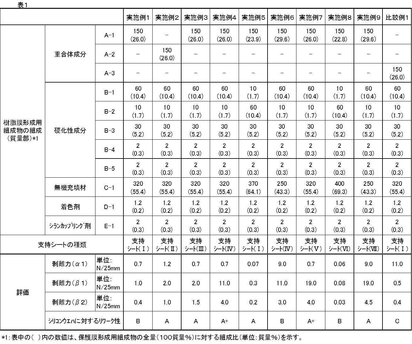
10 支持シート
20 樹脂膜形成用フィルム
21 表面(α)
22 表面(β)
30 樹脂膜
31 表面(α’)
32 表面(β’)
40 治具接着層
50 キャリアシート
100 シリコンウエハ
Claims (9)
- 支持シート上に、樹脂膜を形成し得る樹脂膜形成用フィルムが直接積層した構成を有し、下記要件(I)及び(II)を満たす、樹脂膜形成用複合シート。
要件(I):シリコンウエハと貼付される側の前記樹脂膜形成用フィルムの表面(α)をシリコンウエハ上に貼付した後、23℃の環境下、引張速度300mm/分、及び引張角度180°での剥離条件(x)で測定した、当該シリコンウエハから、当該樹脂膜形成用フィルムを剥離するのに必要な剥離力(α1)が、0.05~10.0N/25mmである。
要件(II):前記剥離条件(x)で測定した、前記支持シートと直接積層している側の前記樹脂膜形成用フィルムの表面(β)から、前記支持シートを剥離するのに必要な剥離力(β1)が、剥離力(α1)以上の値である。 - さらに下記要件(III)を満たす、請求項1に記載の樹脂膜形成用複合シート。
要件(III):前記樹脂膜形成用フィルムから樹脂膜を形成した際、前記剥離条件(x)で測定した、前記支持シートと直接積層している側の前記樹脂膜の表面(β’)から、前記支持シートを剥離するのに必要な剥離力(β2)が、0.02~5.0N/25mmである。 - 剥離力(β1)が、0.05~20.0N/25mmである、請求項1又は2に記載の樹脂膜形成用複合シート。
- 前記支持シートが、基材のみから構成されたシートである、請求項1~3のいずれか1項に記載の樹脂膜形成用複合シート。
- 前記支持シートが、基材上に粘着剤層を有する粘着シートであって、
当該粘着シートの粘着剤層と、前記樹脂膜形成用フィルムの表面(β)とが直接積層した構成を有する、請求項1~3のいずれか1項に記載の樹脂膜形成用複合シート。 - 前記粘着剤層が、エネルギー線硬化型樹脂を含む粘着剤組成物から形成された層である、請求項5に記載の樹脂膜形成用複合シート。
- 前記樹脂膜形成用フィルムが、重合体成分(A)及び硬化性成分(B)を含む、請求項1~6のいずれか1項に記載の樹脂膜形成用複合シート。
- 前記樹脂膜形成用フィルムが、保護膜又は接着膜の形成材料である、請求項1~7のいずれか1項に記載の樹脂膜形成用複合シート。
- 下記工程(1)~(4)を有する、樹脂膜付きチップの製造方法。
工程(1):ワークの裏面に、請求項1~8のいずれか1項に記載の樹脂膜形成用複合シートを貼付する工程
工程(2):ワークをダイシングする工程
工程(3):樹脂膜形成用フィルムから樹脂膜を形成する工程
工程(4):工程(2)を経て得られたダイシングされたワークをピックアップし、チップを得る工程
Priority Applications (4)
| Application Number | Priority Date | Filing Date | Title |
|---|---|---|---|
| CN201680008033.8A CN107210205B (zh) | 2015-02-05 | 2016-02-03 | 树脂膜形成用复合片、以及带树脂膜的芯片的制造方法 |
| SG11201706309VA SG11201706309VA (en) | 2015-02-05 | 2016-02-03 | Resin-film forming composite sheet, and method of manufacturing chip having resin film |
| JP2016573405A JP6423458B2 (ja) | 2015-02-05 | 2016-02-03 | 樹脂膜形成用複合シート、及び樹脂膜付きチップの製造方法 |
| KR1020177021552A KR102594777B1 (ko) | 2015-02-05 | 2016-02-03 | 수지막 형성용 복합 시트, 및 수지막을 갖는 칩의 제조 방법 |
Applications Claiming Priority (2)
| Application Number | Priority Date | Filing Date | Title |
|---|---|---|---|
| JP2015-021479 | 2015-02-05 | ||
| JP2015021479 | 2015-02-05 |
Publications (1)
| Publication Number | Publication Date |
|---|---|
| WO2016125835A1 true WO2016125835A1 (ja) | 2016-08-11 |
Family
ID=56564174
Family Applications (1)
| Application Number | Title | Priority Date | Filing Date |
|---|---|---|---|
| PCT/JP2016/053259 Ceased WO2016125835A1 (ja) | 2015-02-05 | 2016-02-03 | 樹脂膜形成用複合シート、及び樹脂膜付きチップの製造方法 |
Country Status (6)
| Country | Link |
|---|---|
| JP (1) | JP6423458B2 (ja) |
| KR (1) | KR102594777B1 (ja) |
| CN (1) | CN107210205B (ja) |
| SG (1) | SG11201706309VA (ja) |
| TW (1) | TWI689412B (ja) |
| WO (1) | WO2016125835A1 (ja) |
Cited By (6)
| Publication number | Priority date | Publication date | Assignee | Title |
|---|---|---|---|---|
| WO2019082963A1 (ja) * | 2017-10-27 | 2019-05-02 | リンテック株式会社 | 保護膜形成用フィルム、保護膜形成用複合シート、及び半導体チップの製造方法 |
| JP2021082768A (ja) * | 2019-11-21 | 2021-05-27 | リンテック株式会社 | キット、及び、そのキットを用いる第三積層体の製造方法 |
| JPWO2022210087A1 (ja) * | 2021-03-29 | 2022-10-06 | ||
| TWI780127B (zh) * | 2017-03-28 | 2022-10-11 | 日商味之素股份有限公司 | 感光性樹脂組成物 |
| JP2023137425A (ja) * | 2022-03-18 | 2023-09-29 | 株式会社レゾナック | ダイシング・ダイボンディング一体型フィルム及び半導体装置の製造方法 |
| TWI915533B (zh) | 2021-03-29 | 2026-02-21 | 日商琳得科股份有限公司 | 膜狀接著劑、切割黏晶片、半導體裝置之製造方法、以及半導體晶圓之再製方法 |
Families Citing this family (3)
| Publication number | Priority date | Publication date | Assignee | Title |
|---|---|---|---|---|
| KR101936873B1 (ko) * | 2018-03-23 | 2019-01-11 | (주)엠티아이 | 웨이퍼 레벨용 백사이드 점착테이프 및 이의 제조방법 |
| WO2019187247A1 (ja) * | 2018-03-30 | 2019-10-03 | リンテック株式会社 | 硬化封止体の反り防止用積層体、及び、硬化封止体の製造方法 |
| JP7591453B2 (ja) * | 2021-03-31 | 2024-11-28 | リンテック株式会社 | 支持シート、樹脂膜形成用複合シート、キット、及び、樹脂膜付きチップの製造方法 |
Citations (4)
| Publication number | Priority date | Publication date | Assignee | Title |
|---|---|---|---|---|
| JP2010056328A (ja) * | 2008-08-28 | 2010-03-11 | Furukawa Electric Co Ltd:The | チップ保護用フィルム |
| JP2011151362A (ja) * | 2009-12-24 | 2011-08-04 | Nitto Denko Corp | ダイシングテープ一体型半導体裏面用フィルム |
| JP2011228637A (ja) * | 2010-03-30 | 2011-11-10 | Furukawa Electric Co Ltd:The | チップ保護用フィルム |
| WO2013099869A1 (ja) * | 2011-12-26 | 2013-07-04 | リンテック株式会社 | 保護膜形成層付ダイシングシートおよびチップの製造方法 |
Family Cites Families (2)
| Publication number | Priority date | Publication date | Assignee | Title |
|---|---|---|---|---|
| JP2009138026A (ja) | 2007-12-03 | 2009-06-25 | Furukawa Electric Co Ltd:The | エネルギー線硬化型チップ保護用フィルム |
| JP5805367B2 (ja) | 2009-01-30 | 2015-11-04 | 日東電工株式会社 | ダイシングテープ一体型ウエハ裏面保護フィルム |
-
2016
- 2016-02-03 WO PCT/JP2016/053259 patent/WO2016125835A1/ja not_active Ceased
- 2016-02-03 SG SG11201706309VA patent/SG11201706309VA/en unknown
- 2016-02-03 TW TW105103476A patent/TWI689412B/zh active
- 2016-02-03 JP JP2016573405A patent/JP6423458B2/ja active Active
- 2016-02-03 KR KR1020177021552A patent/KR102594777B1/ko active Active
- 2016-02-03 CN CN201680008033.8A patent/CN107210205B/zh active Active
Patent Citations (4)
| Publication number | Priority date | Publication date | Assignee | Title |
|---|---|---|---|---|
| JP2010056328A (ja) * | 2008-08-28 | 2010-03-11 | Furukawa Electric Co Ltd:The | チップ保護用フィルム |
| JP2011151362A (ja) * | 2009-12-24 | 2011-08-04 | Nitto Denko Corp | ダイシングテープ一体型半導体裏面用フィルム |
| JP2011228637A (ja) * | 2010-03-30 | 2011-11-10 | Furukawa Electric Co Ltd:The | チップ保護用フィルム |
| WO2013099869A1 (ja) * | 2011-12-26 | 2013-07-04 | リンテック株式会社 | 保護膜形成層付ダイシングシートおよびチップの製造方法 |
Cited By (14)
| Publication number | Priority date | Publication date | Assignee | Title |
|---|---|---|---|---|
| TWI780127B (zh) * | 2017-03-28 | 2022-10-11 | 日商味之素股份有限公司 | 感光性樹脂組成物 |
| CN111279463A (zh) * | 2017-10-27 | 2020-06-12 | 琳得科株式会社 | 保护膜形成用膜、保护膜形成用复合片及半导体芯片的制造方法 |
| JPWO2019082963A1 (ja) * | 2017-10-27 | 2020-11-19 | リンテック株式会社 | 保護膜形成用フィルム、保護膜形成用複合シート、及び半導体チップの製造方法 |
| WO2019082963A1 (ja) * | 2017-10-27 | 2019-05-02 | リンテック株式会社 | 保護膜形成用フィルム、保護膜形成用複合シート、及び半導体チップの製造方法 |
| JP7137575B2 (ja) | 2017-10-27 | 2022-09-14 | リンテック株式会社 | 保護膜形成用フィルム、保護膜形成用複合シート、及び半導体チップの製造方法 |
| CN111279463B (zh) * | 2017-10-27 | 2023-09-26 | 琳得科株式会社 | 保护膜形成用膜、保护膜形成用复合片及半导体芯片的制造方法 |
| JP2021082768A (ja) * | 2019-11-21 | 2021-05-27 | リンテック株式会社 | キット、及び、そのキットを用いる第三積層体の製造方法 |
| JP7540885B2 (ja) | 2019-11-21 | 2024-08-27 | リンテック株式会社 | キット、及び、そのキットを用いる第三積層体の製造方法 |
| WO2022210087A1 (ja) * | 2021-03-29 | 2022-10-06 | リンテック株式会社 | フィルム状接着剤、ダイシングダイボンディングシート、半導体装置の製造方法、フィルム状接着剤の使用、ダイシングダイボンディングシートの使用、及び、半導体ウエハのリワーク方法 |
| JP2022153305A (ja) * | 2021-03-29 | 2022-10-12 | リンテック株式会社 | ダイシングダイボンディングシート及び半導体装置の製造方法 |
| JPWO2022210087A1 (ja) * | 2021-03-29 | 2022-10-06 | ||
| JP7814996B2 (ja) | 2021-03-29 | 2026-02-17 | リンテック株式会社 | ダイシングダイボンディングシート及び半導体装置の製造方法 |
| TWI915533B (zh) | 2021-03-29 | 2026-02-21 | 日商琳得科股份有限公司 | 膜狀接著劑、切割黏晶片、半導體裝置之製造方法、以及半導體晶圓之再製方法 |
| JP2023137425A (ja) * | 2022-03-18 | 2023-09-29 | 株式会社レゾナック | ダイシング・ダイボンディング一体型フィルム及び半導体装置の製造方法 |
Also Published As
| Publication number | Publication date |
|---|---|
| TWI689412B (zh) | 2020-04-01 |
| TW201702072A (zh) | 2017-01-16 |
| JP6423458B2 (ja) | 2018-11-14 |
| KR102594777B1 (ko) | 2023-10-26 |
| KR20170115048A (ko) | 2017-10-16 |
| SG11201706309VA (en) | 2017-09-28 |
| JPWO2016125835A1 (ja) | 2017-11-16 |
| CN107210205A (zh) | 2017-09-26 |
| CN107210205B (zh) | 2021-06-15 |
Similar Documents
| Publication | Publication Date | Title |
|---|---|---|
| JP6423458B2 (ja) | 樹脂膜形成用複合シート、及び樹脂膜付きチップの製造方法 | |
| JP6562172B2 (ja) | 樹脂膜形成用シート、及び樹脂膜形成用複合シート | |
| JP6389456B2 (ja) | 保護膜形成用複合シート、保護膜付きチップ、及び保護膜付きチップの製造方法 | |
| JP6335173B2 (ja) | 保護膜形成用複合シート、保護膜付きチップ、及び保護膜付きチップの製造方法 | |
| WO2014092200A1 (ja) | 保護膜形成用フィルム | |
| WO2011115159A1 (ja) | 硬化性組成物、ダイシング-ダイボンディングテープ、接続構造体及び粘接着剤層付き半導体チップの製造方法 | |
| JP5580631B2 (ja) | 硬化性組成物、ダイシング−ダイボンディングテープ、接続構造体及び粘接着剤層付き半導体チップの製造方法 | |
| JP2016141749A (ja) | 保護膜形成用シート、及び保護膜形成用複合シート | |
| WO2017145979A1 (ja) | フィルム状接着剤複合シート及び半導体装置の製造方法 | |
| WO2018180594A1 (ja) | フィルム状接着剤複合シート及び半導体装置の製造方法 | |
| JP6464196B2 (ja) | 樹脂膜形成用シート、樹脂膜形成用複合シート、及びシリコンウエハの再生方法 | |
| JP6334197B2 (ja) | 保護膜形成用複合シート、保護膜付きチップ、及び保護膜付きチップの製造方法 | |
| CN112111236A (zh) | 保护膜形成用复合片、及带保护膜的半导体芯片的制造方法 | |
| WO2014142151A1 (ja) | 保護膜形成用複合シート、保護膜形成用複合シートの製造方法および保護膜付チップの製造方法 | |
| JP6978890B2 (ja) | ダイシングダイボンディングシート及び半導体チップの製造方法 | |
| JP6998154B2 (ja) | ダイボンディングシート | |
| JP2022146567A (ja) | 保護膜形成フィルム、保護膜形成用複合シート、保護膜付きワーク加工物の製造方法、及び保護膜付きワークの製造方法 | |
| JP7814992B2 (ja) | 治具固定用粘着シート、保護膜形成用複合シート、及び保護膜付きチップの製造方法 | |
| TW202348756A (zh) | 保護膜形成膜、保護膜形成用複合片、半導體裝置之製造方法、以及保護膜形成膜之使用 | |
| JP2023031526A (ja) | 保護膜形成フィルム、保護膜形成用複合シート、保護膜付きワークの製造方法、及び、保護膜付きワーク加工物の製造方法 |
Legal Events
| Date | Code | Title | Description |
|---|---|---|---|
| 121 | Ep: the epo has been informed by wipo that ep was designated in this application |
Ref document number: 16746666 Country of ref document: EP Kind code of ref document: A1 |
|
| ENP | Entry into the national phase |
Ref document number: 2016573405 Country of ref document: JP Kind code of ref document: A |
|
| ENP | Entry into the national phase |
Ref document number: 20177021552 Country of ref document: KR Kind code of ref document: A |
|
| WWE | Wipo information: entry into national phase |
Ref document number: 11201706309V Country of ref document: SG |
|
| NENP | Non-entry into the national phase |
Ref country code: DE |
|
| 122 | Ep: pct application non-entry in european phase |
Ref document number: 16746666 Country of ref document: EP Kind code of ref document: A1 |