WO2016121037A1 - 反転装置、及び液晶表示パネルの製造方法 - Google Patents
反転装置、及び液晶表示パネルの製造方法 Download PDFInfo
- Publication number
- WO2016121037A1 WO2016121037A1 PCT/JP2015/052392 JP2015052392W WO2016121037A1 WO 2016121037 A1 WO2016121037 A1 WO 2016121037A1 JP 2015052392 W JP2015052392 W JP 2015052392W WO 2016121037 A1 WO2016121037 A1 WO 2016121037A1
- Authority
- WO
- WIPO (PCT)
- Prior art keywords
- substrate
- pair
- heat
- reversing device
- substrates
- Prior art date
- Legal status (The legal status is an assumption and is not a legal conclusion. Google has not performed a legal analysis and makes no representation as to the accuracy of the status listed.)
- Ceased
Links
Images




Classifications
-
- G—PHYSICS
- G02—OPTICS
- G02F—OPTICAL DEVICES OR ARRANGEMENTS FOR THE CONTROL OF LIGHT BY MODIFICATION OF THE OPTICAL PROPERTIES OF THE MEDIA OF THE ELEMENTS INVOLVED THEREIN; NON-LINEAR OPTICS; FREQUENCY-CHANGING OF LIGHT; OPTICAL LOGIC ELEMENTS; OPTICAL ANALOGUE/DIGITAL CONVERTERS
- G02F1/00—Devices or arrangements for the control of the intensity, colour, phase, polarisation or direction of light arriving from an independent light source, e.g. switching, gating or modulating; Non-linear optics
- G02F1/01—Devices or arrangements for the control of the intensity, colour, phase, polarisation or direction of light arriving from an independent light source, e.g. switching, gating or modulating; Non-linear optics for the control of the intensity, phase, polarisation or colour
- G02F1/13—Devices or arrangements for the control of the intensity, colour, phase, polarisation or direction of light arriving from an independent light source, e.g. switching, gating or modulating; Non-linear optics for the control of the intensity, phase, polarisation or colour based on liquid crystals, e.g. single liquid crystal display cells
- G02F1/1303—Apparatus specially adapted to the manufacture of LCDs
-
- G—PHYSICS
- G02—OPTICS
- G02F—OPTICAL DEVICES OR ARRANGEMENTS FOR THE CONTROL OF LIGHT BY MODIFICATION OF THE OPTICAL PROPERTIES OF THE MEDIA OF THE ELEMENTS INVOLVED THEREIN; NON-LINEAR OPTICS; FREQUENCY-CHANGING OF LIGHT; OPTICAL LOGIC ELEMENTS; OPTICAL ANALOGUE/DIGITAL CONVERTERS
- G02F1/00—Devices or arrangements for the control of the intensity, colour, phase, polarisation or direction of light arriving from an independent light source, e.g. switching, gating or modulating; Non-linear optics
- G02F1/01—Devices or arrangements for the control of the intensity, colour, phase, polarisation or direction of light arriving from an independent light source, e.g. switching, gating or modulating; Non-linear optics for the control of the intensity, phase, polarisation or colour
- G02F1/13—Devices or arrangements for the control of the intensity, colour, phase, polarisation or direction of light arriving from an independent light source, e.g. switching, gating or modulating; Non-linear optics for the control of the intensity, phase, polarisation or colour based on liquid crystals, e.g. single liquid crystal display cells
-
- G—PHYSICS
- G02—OPTICS
- G02F—OPTICAL DEVICES OR ARRANGEMENTS FOR THE CONTROL OF LIGHT BY MODIFICATION OF THE OPTICAL PROPERTIES OF THE MEDIA OF THE ELEMENTS INVOLVED THEREIN; NON-LINEAR OPTICS; FREQUENCY-CHANGING OF LIGHT; OPTICAL LOGIC ELEMENTS; OPTICAL ANALOGUE/DIGITAL CONVERTERS
- G02F1/00—Devices or arrangements for the control of the intensity, colour, phase, polarisation or direction of light arriving from an independent light source, e.g. switching, gating or modulating; Non-linear optics
- G02F1/01—Devices or arrangements for the control of the intensity, colour, phase, polarisation or direction of light arriving from an independent light source, e.g. switching, gating or modulating; Non-linear optics for the control of the intensity, phase, polarisation or colour
- G02F1/13—Devices or arrangements for the control of the intensity, colour, phase, polarisation or direction of light arriving from an independent light source, e.g. switching, gating or modulating; Non-linear optics for the control of the intensity, phase, polarisation or colour based on liquid crystals, e.g. single liquid crystal display cells
- G02F1/133—Constructional arrangements; Operation of liquid crystal cells; Circuit arrangements
- G02F1/1333—Constructional arrangements; Manufacturing methods
- G02F1/1339—Gaskets; Spacers; Sealing of cells
-
- G—PHYSICS
- G02—OPTICS
- G02F—OPTICAL DEVICES OR ARRANGEMENTS FOR THE CONTROL OF LIGHT BY MODIFICATION OF THE OPTICAL PROPERTIES OF THE MEDIA OF THE ELEMENTS INVOLVED THEREIN; NON-LINEAR OPTICS; FREQUENCY-CHANGING OF LIGHT; OPTICAL LOGIC ELEMENTS; OPTICAL ANALOGUE/DIGITAL CONVERTERS
- G02F1/00—Devices or arrangements for the control of the intensity, colour, phase, polarisation or direction of light arriving from an independent light source, e.g. switching, gating or modulating; Non-linear optics
- G02F1/01—Devices or arrangements for the control of the intensity, colour, phase, polarisation or direction of light arriving from an independent light source, e.g. switching, gating or modulating; Non-linear optics for the control of the intensity, phase, polarisation or colour
- G02F1/13—Devices or arrangements for the control of the intensity, colour, phase, polarisation or direction of light arriving from an independent light source, e.g. switching, gating or modulating; Non-linear optics for the control of the intensity, phase, polarisation or colour based on liquid crystals, e.g. single liquid crystal display cells
- G02F1/133—Constructional arrangements; Operation of liquid crystal cells; Circuit arrangements
- G02F1/1333—Constructional arrangements; Manufacturing methods
- G02F1/1341—Filling or closing of cells
-
- G—PHYSICS
- G09—EDUCATION; CRYPTOGRAPHY; DISPLAY; ADVERTISING; SEALS
- G09F—DISPLAYING; ADVERTISING; SIGNS; LABELS OR NAME-PLATES; SEALS
- G09F9/00—Indicating arrangements for variable information in which the information is built-up on a support by selection or combination of individual elements
-
- G—PHYSICS
- G02—OPTICS
- G02F—OPTICAL DEVICES OR ARRANGEMENTS FOR THE CONTROL OF LIGHT BY MODIFICATION OF THE OPTICAL PROPERTIES OF THE MEDIA OF THE ELEMENTS INVOLVED THEREIN; NON-LINEAR OPTICS; FREQUENCY-CHANGING OF LIGHT; OPTICAL LOGIC ELEMENTS; OPTICAL ANALOGUE/DIGITAL CONVERTERS
- G02F1/00—Devices or arrangements for the control of the intensity, colour, phase, polarisation or direction of light arriving from an independent light source, e.g. switching, gating or modulating; Non-linear optics
- G02F1/01—Devices or arrangements for the control of the intensity, colour, phase, polarisation or direction of light arriving from an independent light source, e.g. switching, gating or modulating; Non-linear optics for the control of the intensity, phase, polarisation or colour
- G02F1/13—Devices or arrangements for the control of the intensity, colour, phase, polarisation or direction of light arriving from an independent light source, e.g. switching, gating or modulating; Non-linear optics for the control of the intensity, phase, polarisation or colour based on liquid crystals, e.g. single liquid crystal display cells
- G02F1/133—Constructional arrangements; Operation of liquid crystal cells; Circuit arrangements
- G02F1/1333—Constructional arrangements; Manufacturing methods
- G02F1/133354—Arrangements for aligning or assembling substrates
Definitions
- the present invention relates to a reversing device for reversing a substrate pair by sandwiching the substrate pair by a sandwiching member pair, and a method for manufacturing a liquid crystal display panel using the reversing device.
- the liquid crystal display device includes a liquid crystal display panel (hereinafter referred to as a display panel) and a backlight unit.
- the backlight unit is an edge light type
- the backlight unit has a light guide plate, and is configured such that light incident on the side surface of the light guide plate from the light source is emitted from the main surface and irradiates the back surface of the display panel.
- the display panel is an active matrix having a color filter substrate (CF substrate) having a plurality of color filters and a plurality of thin film transistors (Thin Film Transistors, hereinafter referred to as TFTs) which are arranged to face the color filter substrate and are switching elements.
- CF substrate color filter substrate
- TFTs Thin Film Transistors
- Patent Document 2 discloses that after a liquid crystal material is dropped on a TFT substrate and a sealing material is applied to the CF substrate, the CF substrate is reversed so that the coated surface is a lower surface.
- An apparatus configured to be bonded together is disclosed.
- the bonded substrate is inverted so that the TFT substrate is on top, and the sealing material is pre-cured by irradiating with ultraviolet rays from the TFT substrate side.
- the sealing material is pre-cured by irradiating with ultraviolet rays from the TFT substrate side.
- the bonded substrate is inverted so that the CF substrate is on top, and the bonded substrate is heated at 130 ° C. for approximately 70 minutes to fully cure the sealing material.
- the reason why the bonding substrate is reversed is that the CF substrate side is the front side of the display panel, and it is necessary to transport the display panel with the front side facing up to prevent wrinkles. is there.
- the display panel is divided into units.
- the bonded substrate is reversed using a reversing device.
- a reversing device a device equipped with a motor for reversing the bonding substrate by sandwiching the bonding substrate with a plurality of pairs of sandwiching members can be used.
- the sandwiching member is formed by providing a coating layer made of an inexpensive resin such as polyolefin on the surface of the core made of metal.
- the pair of sandwiching members sandwich the bonded substrate in a state where the respective coating layers are in contact with the surface of the bonded substrate, but the contact surface is minute relative to the substrate surface at the time of pressing and reversing the bonded substrate. Sliding may cause wear powder.
- the wear powder is made of polyethylene, polypropylene, etc.
- the melting point of polyethylene is 100 to 120 ° C.
- the melting point of polypropylene is 120 to 130 ° C., which is lower than the above-mentioned thermosetting temperature of 130 ° C. Melt with.
- the molten wear powder adheres to the display panel surface after the bonded substrate is cooled.
- the adhered wear powder is not completely removed by cleaning at the time of dividing the unit and cleaning after mounting the circuit board, and is not visually recognized in an inspection process or the like for visual inspection before and after attaching the polarizing plate. After sticking a polarizing plate on both sides of a bonding substrate, it is visually recognized as a foreign substance and is regarded as a defective product.
- the present invention has been made in view of such circumstances, and when the substrate pair is sandwiched between the pair of sandwiching members, the wear powder generated by contact and sliding of the sandwiching member with respect to the substrate pair heats the substrate pair.
- a reversing device that melts when cooled, adheres to a substrate pair after cooling, and suppresses the occurrence of defects, and a liquid crystal display panel manufacturing method for manufacturing a liquid crystal display panel using the reversing device are provided. The purpose is to do.
- a reversing device includes a pair of sandwiching members that are heated to a predetermined temperature after reversal and sandwich a pair of opposing substrates while maintaining a predetermined interval by a spacer in a state in which the respective axes are parallel to each other.
- the sandwiching member has a heat-resistant layer having a heat-resistant temperature equal to or higher than the predetermined temperature on the opposite side.
- the heat-resistant layer has a heat-resistant layer having a heat-resistant temperature equal to or higher than the predetermined temperature, the wear powder generated by sliding the holding member against the substrate pair when the substrate pair is held by the pair of holding members When the pair is heated to the predetermined temperature, it does not melt, and after the substrate pair is cooled, it is suppressed that the wear powder adheres to the substrate pair and becomes a defective product.
- the reversing device according to the present invention is characterized in that a coefficient of static friction of the heat-resistant layer with respect to the substrate pair is 0.3 or more.
- a frictional force can be generated without applying an excessive pressing force, so that the clamping member is prevented from sliding and shifting with respect to the substrate pair. Is done.
- the static frictional force of the heat-resistant layer with respect to the substrate pair in a state where the substrate pair is sandwiched is greater than 9.81 ⁇ (mass [kg] of the substrate pair) [N]. It is characterized by that.
- the bonded substrate is prevented from dropping due to gravity during the reversal.
- the reversing device according to the present invention is characterized in that the heat-resistant layer has glass fiber or carbon fiber.
- the wear resistance is good and the service life is long, and the apparatus can be stably operated by taking a long replacement and cleaning cycle.
- the reversing device is characterized in that the heat-resistant layer includes a material selected from the group consisting of glass fiber impregnated with polytetrafluoroethylene, polyimide, nylon, aluminum, and stainless steel.
- the coefficient of static friction is high, and it is well suppressed that deviation occurs when the bonded substrate is sandwiched.
- the reversing device according to the present invention is characterized in that the clamping member is formed by providing the heat-resistant layer on a metal core.
- the substrate pair can be uniformly contacted in a wide range, and an excessive pressing force can be prevented from being generated locally, and the clamping strength is high.
- a frictional force can be secured with a predetermined contact force, and a predetermined interval between the pair of substrates is set. Since the prescribed spacer can be prevented from being deformed, the occurrence of uneven thickness between the pair of substrates is suppressed, and the sliding of the pair of substrates is suppressed.
- the reversing device according to the present invention is characterized by having an intermediate layer containing polyolefin or elastomer between the core material and the heat-resistant layer.
- uneven distribution of the contact pressure between the pair of substrates can be suppressed, generation of an excessively large pressing force can be suppressed, a frictional force can be secured with a predetermined contact force, and Since it is possible to prevent the spacer defining the predetermined interval from being deformed, the occurrence of uneven thickness between the pair of substrates is suppressed, and the slip of the substrate pair is suppressed. Furthermore, since the intermediate layer is covered with the heat-resistant layer, when the intermediate layer is a polyolefin or an elastomer, generation of sticking matters due to the intermediate layer is suppressed.
- the reversing device according to the present invention is characterized in that the heat-resistant layer is subjected to an antistatic treatment or has conductivity.
- the substrate pair is prevented from being charged.
- the reversing device is characterized in that it includes a displacement prevention portion that abuts against the end surfaces of the substrate pair and prevents the substrate pair from slipping off.
- the substrate reversing step uses the reversing device described above, The pair of substrates is inverted.
- the wear powder between the clamping member and the substrate melts and adheres to the substrate after cooling. Therefore, the occurrence of defective products is suppressed.
- the method for manufacturing a liquid crystal display panel according to the present invention includes a step of irradiating the pair of substrates with ultraviolet light between the substrate bonding step and the heating step, and a second substrate inversion for inverting the pair of substrates.
- the second substrate reversing step includes reversing the pair of substrates using the reversing device.
- the abrasion powder between the sandwiching member and the substrate is melted in a subsequent heating step, and after cooling, Sticking is suppressed.
- each holding member has a heat-resistant layer having a heat-resistant temperature equal to or higher than a predetermined temperature on the opposite side, so that when the pair of holding members holds the pair of substrates, the holding members are paired with the substrate.
- the wear powder generated by sliding against the substrate melts when the substrate pair is heated, and after cooling, the wear powder is prevented from adhering to the substrate pair and becoming a defective product.
- the occurrence of defects due to abrasion powder between the holding member of the reversing device and the substrate is suppressed.
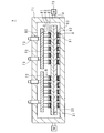
- FIG. 1 is a schematic perspective view showing a television receiver (hereinafter referred to as a TV receiver) according to Embodiment 1 of the present invention. It is typical sectional drawing which shows the display panel which concerns on Embodiment 1 of this invention. It is a typical sectional view of a reversing device for reversing a bonded TFT substrate and CF substrate. It is a partially expanded sectional view of FIG. It is a schematic plan view which shows the bonding board
- FIG. 1 is a schematic perspective view showing a TV receiver 1 according to Embodiment 1 of the present invention
- FIG. 2 is a schematic sectional view showing a display panel 3 according to Embodiment 1. As shown in FIG.
- the TV receiver 1 includes a horizontally long display module 2 that displays video, a tuner 11 that receives broadcast waves from an antenna (not shown), and a decoder 12 that decodes encoded broadcast waves.
- the TV receiver 1 decodes the broadcast wave received by the tuner 11 by the decoder 12 and displays an image on the display module 2 based on the decoded information.
- a stand 13 that supports the TV receiver 1 is provided below the TV receiver 1.
- the display module 2 when the display module 2 is an edge light type, the display module 2 includes a display panel 3, for example, two optical sheets (hereinafter, not shown), a light guide plate, a reflection sheet, and a chassis.
- the display module 2 is accommodated in a vertical posture in a front cabinet 4 and a rear cabinet 5 that are arranged in a vertical posture in the front-rear direction.
- the front cabinet 4 is a rectangular frame that covers the peripheral edge of the display module 2, and has a rectangular opening 2a in the center.
- the front cabinet 4 is made of, for example, a plastic material.
- the rear cabinet 5 has a rectangular tray shape with the front side open, and is made of, for example, a plastic material. In addition, you may comprise the front cabinet 4 and the back cabinet 5 from another material.
- the vertical and horizontal dimensions of the front cabinet 4 and the rear cabinet 5 are substantially the same, and the peripheral portions of each other face each other.
- the vertical and horizontal dimensions of the display panel 3 are slightly larger than the opening 2 a of the front cabinet 4, and the peripheral portion of the display panel 3 faces the inner edge portion of the front cabinet 4.
- the display panel 3 includes an active matrix (TFT) substrate 30 and a color filter (CF) substrate 31 facing each other, a liquid crystal layer 32 disposed as a display medium layer between the TFT substrate 30 and the CF substrate 31, and a TFT substrate 30. And a CF material 31 and a sealing material 33 provided in a frame shape for sealing the liquid crystal layer 32 between the TFT substrate 30 and the CF substrate 31.
- TFT active matrix
- CF color filter
- FIG. 3 is a schematic cross-sectional view of a reversing device 7 for reversing the bonded TFT substrate 30 and CF substrate 31 (hereinafter referred to as a bonded substrate), and FIG. 4 is a partially enlarged cross-sectional view of FIG. In FIG. 3, the liquid crystal layer 32 is omitted.
- the reversing device 7 includes a main body 71, two shaft portion support portions 72, four air cylinders 73, two motors 75, a plurality of substrate contact portions 8, and a plurality of substrate support portions 9.
- the main body 71 has a rectangular tube shape with both end faces open, and is placed horizontally.
- ten substrate support portions 9 each having a bar shape extending in the front and back direction of the paper surface of FIG.
- the substrate support portion 9 covers a rectangular core portion 91 having a convex curve with the upper side convex upward, a first covering portion 92 that covers the upper surface of the core portion 91, and an upper surface of the first covering portion 92.
- a second covering portion 93 is a rectangular core portion 91 having a convex curve with the upper side convex upward.
- the substrate abutting portion 8 is provided at a shaft portion 80 extending in the vertical direction, one end portion of the shaft portion 80, and a rectangular core portion 81 having a convex curve with a lower side in a side view, and a core portion 81.
- coated part 82 are provided.
- the lengths of the substrate support portion 8 and the substrate contact portion 9 are slightly longer than the depth of the main body 71.
- the substrate support portion 8 and the core portion 81 and the core portion 91 of the substrate contact portion 9 are both made of aluminum.
- Both the first covering portion 82 and the second covering portion 92 are made of an inexpensive low density polyolefin material.
- the second covering parts 83 and 93 are made of a heat resistant material having a heat resistant temperature of 130 ° C. or higher.
- the heat resistant temperature refers to a temperature at which deformation such as softening is observed. That is, the melting point, the softening point, or the thermal decomposition temperature is 130 ° C. or higher, which is higher than the thermosetting temperature of the sealing material 33 described later.
- the heat resistant temperature is preferably 140 ° C. or higher. Since the heat-resistant temperature is 130 ° C. or higher, the wear powder generated by the second covering portions 83 and 93 when the bonded substrate is sandwiched or reversed is caused by the CF substrate 31 or the TFT substrate 30 in the curing step of the sealing material 33 described later.
- heat-resistant materials having a heat-resistant temperature of the second covering portions 83 and 93 of 130 ° C. or higher include nylons such as nylon 6, nylon 6, 6, and the like, polyimide, fluororesin [including PTFE (polytetrafluoroethylene)], polyphenylene Examples thereof include synthetic resins such as oxide (PPO), polysulfone, polypropylene, phenolic resin (novolac type), fiber reinforced plastic (FRP), and flexible metal thin plates and metal sheets such as Al and SUS.
- the coefficient of static friction with respect to the glass of the heat-resistant material is preferably 0.3 or more, more preferably 0.4 or more in order to obtain a predetermined friction force with a pressing force that does not cause cell thickness unevenness, More preferably, it is 1.0 or more. Thereby, it is suppressed that a shift
- the static friction coefficient is such that the substrate contact portion 8 and the substrate support portion 9 have good releasability from the substrate, and the substrate contact portion 8 and the substrate support portion 9 do not have contact marks. It is preferable that it is 1.8 or less.
- coated parts 83 and 93 is larger than [9.81x (mass [kg] of a bonding board
- the pressing force with which the clamping member pair comes into contact with the substrate pair is 100 N / cm 2 or less.
- the heat-resistant material contains a synthetic resin
- the heat-resistant material has conductivity or has been subjected to antistatic treatment. Accordingly, charging of the bonded substrate is prevented, and the TFT element of the TFT substrate 30 is prevented from being destroyed by discharge, and floating foreign matter in the air can be prevented from being attracted and attracted by static electricity.
- the heat resistant material is preferably a material selected from the group consisting of glass fibers impregnated with PTFE, polyimide, nylon, Al, SUS and the like.
- the thicknesses of the substrate contact portion 8 and the substrate support portion 9 there are cases where the core portions 81 and 91 are 15 mm, the first covering portions 82 and 92 are 2 mm, and the second covering portions 83 and 93 are 0.2 mm. .
- the substrate mass is 20 kg
- the substrate contact force of the substrate contact portion 8 and the substrate support portion 9 by the air cylinder 73 is 2000 N in total
- the maximum contact force in consideration of gravity and impact force at the time of contact is 6000 N.
- the actual contact area measured with pressure-sensitive paper is 100 cm 2 per side for each of the substrate contact portion 8 and the substrate support portion 9. In this case, the maximum contact pressure to the substrate is 60 N / cm 2 .
- the static friction force at a static friction coefficient of 0.3 is 600 N
- the gravity due to the substrate mass is 196.2 N. Since the contact pressure to the substrate is 60 N / cm 2 at the maximum, it is smaller than 100 N / cm 2 which causes the cell thickness unevenness, so that the cell thickness unevenness can be prevented.
- the maximum static frictional force is 600 N, which is larger than the substrate gravity of 196.2 N, so that it is possible to prevent slipping and dropping due to gravity.
- the maximum static frictional force is preferably three times or more of the substrate weight.
- each shaft portion support portion 72 includes five shaft portions 80.
- the suspension is supported in a state of being hung from the shaft support portion 72.
- Two air cylinders 73 are provided on the upper plate portion of the main body 71, and the lower end portion of the shaft portion of the air cylinder 73 is connected to the shaft support portion 72.
- the shaft support portion 72 is moved up and down by the air cylinder 73, whereby the substrate contact portion 8 is configured to come into contact with and separate from the TFT substrate 30 and the CF substrate 31 inserted between the substrate support portion 9.
- Motors 75 are respectively provided on both sides of the main body 71. When the shaft portion 74 of the motor 75 rotates, the upper and lower sides of the main body 71 are switched.
- the substrate abutting portion 8 is raised by the air cylinder 73, and the substrate supporting portion 9 and A gap is provided between the two, and a bonded substrate is inserted into the gap and placed on the substrate support 9.
- the substrate contact portion 8 is lowered by the air cylinder 73, and the bonded substrate is sandwiched between the substrate support portion 9.
- the axial part 74 is rotated so that the upper and lower sides of the main body 71 may be switched with the motor 75, and a bonding board
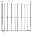
- FIG. 5A is a schematic plan view showing the bonded substrate before reversal and the substrate contact portion 8
- FIG. 5B is a schematic plan view showing the bonded substrate after reversal and the substrate support portion 9.
- 5A and 5B show a first inversion case described later.
- the alternate long and short dash line indicates the rotation axis
- the alternate long and two short dashes line indicates the boundary of each row.
- the CF substrate 31 and the substrate contact portion 8 are on the upper side, but the TFT substrate 30 and the substrate support portion 9 are on the upper side due to inversion.
- FIG. 6 is a flowchart showing a method for manufacturing the display panel 3.
- the sealing material 33 is applied in a frame shape to the peripheral end portion of the CF substrate 31 by screen printing or the like (S1).
- the sealing material 33 is made of a synthetic resin having ultraviolet curing properties and thermosetting properties.
- a liquid crystal material is dropped in a dot shape at a predetermined interval inside the sealing material 33 of the CF substrate 31 (S2).
- the CF substrate 31 and the TFT substrate 30 are accommodated in a processing chamber, and the processing chamber is evacuated to a vacuum state of, for example, 1 Pa.
- the CF substrate 31 onto which the liquid crystal material 32 has been dropped and the TFT substrate 30 are bonded together under vacuum (S3).
- the CF substrate 31 is on the upper side.
- the vacuum state in the processing chamber is released, and a uniform pressure is applied to the CF substrate 31 and the TFT substrate 30 from the outside due to a pressure difference.
- the dropped liquid crystal materials 32 come into contact with each other and diffuse.
- There is a gap between the sealing material 33 and the peripheral edge of the liquid crystal material 32, and the region where the liquid crystal material 32 does not spread is a bubble region.
- the laminated substrate taken out from the processing chamber is bonded to the TFT substrate 30 side after bonding so that the CF substrate 31 is on the upper side and the TFT substrate 30 is on the lower side by using the reversing device 7 described above. Inversion is performed so that 30 is on the top and the CF substrate 31 is on the bottom (first inversion, “second substrate inversion step” in claim 11: S4). Then, the sealing material 33 is irradiated with ultraviolet rays, and the sealing material 33 is pre-cured (S5).
- the TFT substrate 30 is up and the CF substrate 31 is down so that the CF substrate 31 is up and the TFT substrate 30 is down (second inversion, claim 10).
- the display panel 3 is accommodated in a heating chamber and heated at 130 ° C. for about 70 minutes to fully cure the sealing material 33 (S7). Since the temperature of the liquid crystal material 32 rapidly rises to 130 ° C., the liquid crystal material 32 is thermally expanded and diffused between the pair of CF substrates 31 and the TFT substrate 30. Finally, the display panel 3 is divided into units (S8). The display panel 3 is manufactured as described above (S9).
- the reversing device 7 of the present embodiment is configured as described above, when pressed to pinch the bonded substrate, or during reversal, the generation of wear powder due to sliding is suppressed, Even when wear powder is generated, the heat resistance temperature of the second covering portions 83 and 93 of the substrate contact portion 8 and the substrate support portion 9 is higher than the thermosetting temperature of the seal material 33, so the wear powder is heated by the heat of the seal material 33. It is prevented from melting and adhering to the bonded substrate during curing. Therefore, the occurrence of defects is suppressed.
- the inner eight of the ten substrate support portions 9 are the core portion 91, the first covering portion 92, and the second covering portion.
- the three-layer structure of the portion 93 is formed, and a two-layer structure in which the surface of the core portion 91 is covered only by the first covering portion 92 on the outer sides of the eight substrate support portions 9, that is, on both end portions of the lower plate portion. You may decide.
- the inner eight of the ten substrate contact portions 8 have a three-layer structure including a core portion 81, a first cover portion 82, and a second cover portion 83.
- a two-layer structure in which the surface of the core portion 81 is covered only by the first covering portion 82 may be provided on both end portions of the lower plate portion. Since the static friction coefficient of the 1st coating
- the substrate contact portion 8 and the substrate support portion 9 on both ends need not have a two-layer structure.
- Polyimide has a thermal decomposition temperature of around 400 ° C. and has very good heat resistance. Furthermore, when using conductive polyimide, charging of the bonded substrate due to contact can be prevented.
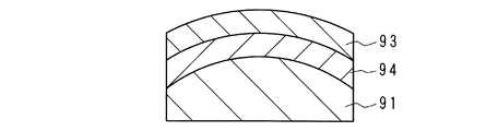
- FIG. 7 is a schematic cross-sectional view showing the substrate contact portion 9 according to Embodiment 2 of the present invention.
- the substrate contact portion 9 includes a rectangular core portion 91 having a convex curve with the upper side protruding upward, a first covering portion 94 that covers the upper surface of the core portion 91, and the upper surface of the first covering portion 94. And a second covering portion 93 for covering.
- the substrate support portion 8 also has a rectangular core portion 81 whose side view forms a downwardly convex curve, and a first covering portion 84 that covers the lower surface of the core portion 81. And a second covering portion 83 that covers the lower surface of the first covering portion 82 (not shown).
- the substrate support portion 8 and the core portion 81 and the core portion 91 of the substrate contact portion 9 are both made of aluminum.
- Both the first covering portion 84 and the second covering portion 94 are made of fluorine rubber such as Teflon (registered trademark) rubber or rubber such as silicone rubber.
- the second covering parts 83 and 93 are made of a heat resistant material having a heat resistant temperature of 130 ° C. or higher.
- the heat resistant temperature is preferably 140 ° C. or higher. Since the heat-resistant temperature is 130 ° C. or higher, the abrasion powder is prevented from being fused to the CF substrate 31 or the TFT substrate 30 in the thermosetting process of the sealing material 33 described later.
- Examples of the heat-resistant material having a heat-resistant temperature of 130 ° C. or higher when the second covering portions 83 and 93 are melted include synthetic resins such as nylon 6, 6 and polyimide, and metal thin plates such as Al and SUS.
- the static friction coefficient of the heat-resistant material with respect to the glass is preferably 0.3 or more, more preferably 0.4 or more, and further preferably 1.0 or more.
- the static frictional force of the heat resistant material is preferably larger than [9.81 ⁇ (mass of bonded substrate [kg])] (N).
- the heat resistant material preferably has glass fiber or carbon fiber. It is preferable that the heat-resistant material has conductivity or has been subjected to antistatic treatment.
- the heat-resistant material is preferably a material selected from the group consisting of glass fibers impregnated with PTFE, polyimide, and metal thin plates such as nylon, Al, and SUS.
- coated parts 82 and 92 As an example of the thickness of the 2nd coating
- the substrate mass is 20 kg
- the substrate contact force of the substrate contact portion 8 and the substrate support portion 9 by the air cylinder 73 is 2000 N in total, and the maximum contact force considering the gravity and impact force at the time of contact is 5000 N.
- the actual contact area measured with pressure-sensitive paper is 300 cm 2 per side with 10 each of the substrate contact portion 8 and the substrate support portion 9. In this case, the maximum contact pressure to the substrate is 17 N / cm 2 .
- the static friction force at a static friction coefficient of 0.3 is 600 N
- the gravity due to the substrate mass is 196.2 N.
- the contact pressure to the substrate is a maximum 17N / cm 2, significantly less than 100 N / cm 2 to produce a cell thickness unevenness, it is possible to prevent occurrence of cell thickness irregularity.
- the maximum static frictional force is 600 N, it is larger than 196.2 N of the substrate gravity, so that it is possible to prevent slipping and dropping due to gravity.
- the maximum static frictional force is preferably three times or more of the substrate weight.
- the contact pressure to the substrate is unevenly distributed as in the case where the contact surface with the substrate is hard, and cell thickness unevenness may occur.
- the frictional force can be uniformly applied, the sliding of the substrate contact portion 8 and the substrate support portion 9 is suppressed.
- the rubber layer is the outermost layer, unevenness caused by the low molecular weight component of the rubber material adhering to the substrate does not occur on the surface, and the quality of the display panel does not deteriorate.
- the contact surface has elasticity, a local impact force at the time of contact can be suppressed, and an impact force when the bonded substrate is loaded on the lower substrate support member 9 before the substrate is sandwiched can also be suppressed. Thereby, since the substrate moving speed at the time of substrate loading can be set high, the substrate flow tact can be shortened.
- a thin metal plate such as Al or SUS is used as the second covering portions 82 and 92, it is preferable because the heat resistance temperature and the static friction coefficient are high and the durability is good.
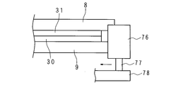
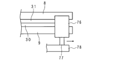
- the display panel according to Embodiment 3 of the present invention includes a displacement prevention unit 76 that contacts the end surfaces of the substrate contact portion 8 and the substrate support portion 9 and prevents the substrate contact portion 8 and the substrate support portion 9 from falling off. Except for this, it has the same configuration as the display panel 3 according to the first embodiment.
- FIG. 8 is a schematic plan view showing the bonding substrate before reversal and the substrate contact portion 8
- FIG. 9A is a schematic side view showing a state before the slip prevention portion 76 contacts the end surface of the bonding substrate, and FIG. 9B. It is a typical side view which shows the state which the slip prevention part 76 contact
- 9A and 9B are side views of the upper right portion of FIG. 8 as viewed from the right side.
- the CF substrate 31 and the TFT substrate 30 (bonded substrate) are sandwiched between the substrate contact portion 8 and the substrate support portion 9, and the upper long side in FIG. ) Are provided on both end portions of the end surface corresponding to () near the substrate contact portions 8 at both end portions.
- the slip prevention portion 76 is a heat-resistant resin cylindrical member such as nylon or PEEK material, and is fixed to a stainless support shaft 77.
- the support shaft 77 is an air cylinder (not shown) provided on the main body 71.
- the shaft portion 78 is supported.
- the slip prevention part 76 can be brought into contact with and separated from the end face of the bonded substrate by an air cylinder. That is, the shift prevention unit 76 advances and retreats in a direction perpendicular to the end surface.
- the bonded substrate is stacked between the substrate contact portion 8 and the substrate support 9 in a state in which the displacement prevention member 76 is in a position separated from the end surface position of the bonded substrate.
- substrate contact part 8 moves, contacts a bonding board
- the displacement preventing portion 76 is moved by the air cylinder to a position in contact with the bonded substrate end face sandwiched between the substrate contact portion 8 and the substrate support portion 9.
- the slip prevention unit 76 is fixed and rotates while in contact with the end face of the bonded substrate, and the bonded substrate is prevented from slipping and dropping during the reverse rotation.
- the slip prevention unit 76 is moved to a position away from the substrate end surface by the air cylinder. After the separation preventing part 76 is separated, the bonded substrate is taken out from the reversing device 7.
- the shift preventing portion 76 is provided at one end of the substrate contact portion 8 and the substrate support portion 9, when the shaft portion 74 is rotated to reverse the bonded substrate, the bonding is performed.
- the board does not slip off.
- the shift prevention unit 76 is not limited to two, and three or more may be provided.
- the CF substrate 31 is up and the TFT substrate 30 is down at the time of bonding, and the reversing device 7 is provided before UV irradiation after bonding and after UV irradiation, respectively.
- a configuration in which the reversing device 7 is provided only after the UV irradiation after bonding with the CF substrate 31 on the bottom and the TFT substrate 30 on the top is also possible.
- the inner eight portions are made of aluminum and the first covering portions 82 and 92 are made of thermoplastic low-density polyolefin.
- the second covering parts 83 and 93 are made of a glass fiber material impregnated with PTFE (“TG cloth (antistatic adhesive type)” manufactured by Yodogawa Hutec Co., Ltd.).
- PTFE TG cloth (antistatic adhesive type) manufactured by Yodogawa Hutec Co., Ltd.
- the two outer substrate contact portions 8 and the substrate support portion 9 do not have the second covering portions 83 and 93, and the core portions 81 and 91 are covered only by the first covering portions 82 and 92.
- the core portions 81 and 91 have a thickness of 15 mm
- the first covering portions 82 and 92 have a thickness of 2 mm
- the second covering portions 83 and 93 have a thickness of 0.2 mm.
- the ten substrate contact portions 8 of the reversing device and the core portions 81 and 91 of the substrate support portion 9 were covered only with the first covering portions 82 and 92.
- the core portions 81 and 91 have a thickness of 15 mm, and the first covering portions 82 and 92 have a thickness of 2 mm.
- the coefficient of static friction is a coefficient for glass.
- the sticking of the substrate it was confirmed whether or not the substrate sticks to the substrate contact portion 8 and the substrate support portion 9 (whether the release property is good) when the holding of the substrate is released. There was no sticking of the substrate in the examples and comparative examples. The presence or absence of the substrate trace was confirmed using a searchlight in a dark place whether or not the trace of the substrate contact portion 8 and the substrate support portion 9 was transferred to the substrate. In both the examples and comparative examples, no traces of the substrate contact portion 8 and the substrate support portion 9 were found by transmission and reflection, and it was confirmed that there was no unevenness caused by the traces when the polarizing plate was attached and the lighting was confirmed. It was done.
- the numbers in Examples and Comparative Examples in Table 2 indicate batch groups (first batch group, second batch group,...) In which a display panel 3 is manufactured by attaching a polarizing plate to the outside of the TFT substrate 30 and the CF substrate 31. ing.
- the 0-row cell, 1-row cell, 2-row cell, and 3-row cell in Table 2 are the rows of cells when the units of each display panel 3 are cut out from the mother glass (see FIGS. 5A and 5B). From Table 2, it can be seen that the production method of the embodiment suppresses the generation of foreign matter, and in particular, the foreign matter in the first-row cell and the second-row cell where the inner three-layer structure substrate contact portion 8 and substrate support portion 9 contact. It turns out that there is no outbreak.
- each of the three substrate contact portions 8 and the substrate support portion 9 has a two-layer structure in which the second covering portions 83 and 93 are not provided. Occurrence has occurred, but due to the effect of the other two being the configuration of the example, the incidence of foreign matter is reduced compared to the comparative example. From the above, it was confirmed that the production method of the display panel of the present invention suppresses the generation of foreign matters on the substrate surface and reduces the defect rate.
- the first to third embodiments disclosed herein are illustrative in all respects and should not be considered restrictive.
- the scope of the present invention is not intended to include the above-described meaning, but is intended to include meanings equivalent to the scope of the claims and all modifications within the scope of the claims.
- the number of substrate contact portions 8, substrate support portions 9, air cylinders 73, etc. is not limited to the numbers described in the first to third embodiments.
- the shapes of the core portions 81 and 91 are not limited to the shapes described in the first to third embodiments, and may be quadrangular or pentagonal.
- substrate support part 9 are not limited when it is a three-layer structure, You may cover the surface of a core part with one coating
- the covering portion is preferably made of a material that satisfies the above-mentioned conditions for heat resistance, static friction coefficient, and static friction force, has good releasability, and does not leave a mark on the bonded substrate.
- the liquid crystal material may be injected after the CF substrate 31 and the TFT substrate 30 are bonded together.
- the reversing device 7 is not limited to use when the display panel 3 is manufactured.
Landscapes
- Physics & Mathematics (AREA)
- Nonlinear Science (AREA)
- General Physics & Mathematics (AREA)
- Chemical & Material Sciences (AREA)
- Crystallography & Structural Chemistry (AREA)
- Optics & Photonics (AREA)
- Engineering & Computer Science (AREA)
- Mathematical Physics (AREA)
- Manufacturing & Machinery (AREA)
- Theoretical Computer Science (AREA)
- Liquid Crystal (AREA)
- Devices For Indicating Variable Information By Combining Individual Elements (AREA)
Abstract
挟持部材対により基板対を挟持したときに挟持部材が基板対に対し接触・摺動して生じた摩耗粉が、基板対を加熱したときに溶融し、冷却後、基板対に固着して不良が発生することが抑制された反転装置、及び該反転装置を用いて液晶表示パネルを製造する、液晶表示パネルの製造方法を提供する。反転装置(7)は、本体(71)、軸部支持部(72)、エアシリンダ(73)、モータ(75)、複数の基板当接部(8)、及び複数の基板支持部(9)を備える。夫々の軸心が平行である状態で、基板対を基板当接部(8)及び基板支持部(9)により挟持し、モータ(75)により、挟持された基板対を反転させる。基板当接部(8)及び基板支持部(9)は、耐熱温度が基板対が反転された後に加熱される温度以上である耐熱層(第2被覆部83,93)を有する。
Description
本発明は、基板対を挟持部材対により挟んで基板対を反転させる反転装置、及び該反転装置を用いて液晶表示パネルを製造する方法に関する。
表示装置の中で、液晶表示装置は薄型であり、消費電力が低いという特徴を有する。
液晶表示装置は、液晶表示パネル(以下、表示パネルという)と、バックライトユニットとを備える。バックライトユニットがエッジライト型である場合、導光板を有し、光源から導光板の側面に入射された光が主面から出射し、表示パネルの背面を照射するように構成されている。
液晶表示装置は、液晶表示パネル(以下、表示パネルという)と、バックライトユニットとを備える。バックライトユニットがエッジライト型である場合、導光板を有し、光源から導光板の側面に入射された光が主面から出射し、表示パネルの背面を照射するように構成されている。
表示パネルは、複数のカラーフィルタを有するカラーフィルタ基板(CF基板)と、カラーフィルタ基板に対向して配置され、スイッチング素子である複数の薄膜トランジスタ(Thin Film Transistor、以下、TFTという)を有するアクティブマトリクス基板(TFT基板)と、スペーサにより所定のギャップを保持して対向するCF基板とTFT基板との間に表示媒体層として設けられた液晶層とを備える。
特許文献1等の表示パネルの製造方法に記載されているように、表示パネルを作製する場合、まず、CF基板の周縁部の内側にシール材を塗布し、シール材の内側に液晶材料を点状に滴下する。シール材は紫外線硬化性及び熱硬化性を有する。
そして、CF基板を上にした状態で、CF基板とTFT基板とを真空下で貼り合わせる(以下、貼り合わせた基板を貼合基板という)。CF基板の反転装置として、特許文献2には、TFT基板に液晶材料を滴下し、CF基板にシール材を塗布した後、塗布面が下面になるようにCF基板を反転させて、TFT基板と貼り合わせるように構成した装置が開示されている。
そして、CF基板を上にした状態で、CF基板とTFT基板とを真空下で貼り合わせる(以下、貼り合わせた基板を貼合基板という)。CF基板の反転装置として、特許文献2には、TFT基板に液晶材料を滴下し、CF基板にシール材を塗布した後、塗布面が下面になるようにCF基板を反転させて、TFT基板と貼り合わせるように構成した装置が開示されている。
次に、TFT基板が上になるように貼合基板を反転し、TFT基板側から紫外線を照射して、シール材を予備硬化させる。狭額縁化のため、CF基板のブラックマトリクスとシール材とが重なるように設けられた構成では、TFT基板が上になるように反転させて、TFT基板側から紫外線を照射する必要がある。
紫外線照射後、CF基板が上になるように貼合基板を反転させて、貼合基板を130℃で略70分間加熱し、シール材を本硬化させる。ここで、貼合基板を反転させるのは、CF基板側が表示パネルの表側であり、疵が付くのを防止するために、表を上にした状態で、表示パネルを運搬する必要があるからである。
最後に、表示パネルをユニット毎に分断する。
最後に、表示パネルをユニット毎に分断する。
以上のように、貼合基板は反転装置を用いて反転させられる。反転装置として、複数対の挟持部材で貼合基板を挟持して貼合基板を反転させるモータを備えるものを用いることができる。
挟持部材は金属からなる芯部の表面に、安価なポリオレフィン等の樹脂からなる被覆層を設けてなる。
挟持部材は金属からなる芯部の表面に、安価なポリオレフィン等の樹脂からなる被覆層を設けてなる。
一対の挟持部材は、夫々の被覆層が貼合基板の表面に接触する状態で、貼合基板を挟持するが、貼合基板への押圧時及び反転時に、接触面が基板表面に対し微小に摺動して、摩耗粉が生じることがある。摩耗粉はポリエチレン、ポリプロピレン等からなり、ポリエチレンの融点は100~120℃、ポリプロピレンの融点は120~130℃であり、上述の熱硬化温度の130℃より低いため、熱硬化時に表示パネルの表面上で溶融する。
溶融した磨耗粉は、貼合基板の冷却後、表示パネル表面に固着する。固着した摩耗粉は、ユニットの分断時の洗浄、回路基板実装後の洗浄では完全には除かれず、偏光板貼り付け前の良否を目視検査する検査工程等では視認されない。貼合基板の両側に偏光板を貼り付けた後に異物として視認され、不良品とされる。
溶融した磨耗粉は、貼合基板の冷却後、表示パネル表面に固着する。固着した摩耗粉は、ユニットの分断時の洗浄、回路基板実装後の洗浄では完全には除かれず、偏光板貼り付け前の良否を目視検査する検査工程等では視認されない。貼合基板の両側に偏光板を貼り付けた後に異物として視認され、不良品とされる。
本発明は斯かる事情に鑑みてなされたものであり、一対の挟持部材により基板対を挟持したときに挟持部材が基板対に対し接触・摺動して生じた摩耗粉が、基板対を加熱したときに溶融し、冷却後、基板対に固着して、不良が発生することが抑制された反転装置、及び該反転装置を用いて液晶表示パネルを製造する、液晶表示パネルの製造方法を提供することを目的とする。
本発明に係る反転装置は、反転後に所定温度に加熱され、スペーサにより所定の間隔を保持して対向する基板対を夫々の軸心が平行である状態で挟持する挟持部材対と、該挟持部材対に挟持された前記基板対を反転させる反転部とを備える反転装置において、前記挟持部材は、対向する側に夫々耐熱温度が前記所定温度以上である耐熱層を有することを特徴とする。
本発明においては、耐熱温度が前記所定温度以上である耐熱層を有するので、一対の挟持部材により基板対を挟持したときに挟持部材が基板対に対し摺動して生じた摩耗粉が、基板対を前記所定温度に加熱したときに溶融せず、基板対の冷却後、摩耗粉が基板対に固着して不良品となることが抑制されている。
本発明に係る反転装置は、前記耐熱層の前記基板対に対する静止摩擦係数は0.3以上であることを特徴とする。
本発明においては、一対の挟持部材により基板対を挟持したときに、過大な押圧力を付与することなく摩擦力を生じさせられるので、挟持部材が基板対に対し摺動、及びずれることが抑制される。
本発明に係る反転装置は、前記基板対を挟持した状態での、前記基板対に対する前記耐熱層の静止摩擦力は、9.81×(前記基板対の質量[kg])[N]より大きいことを特徴とする。
本発明においては、反転途中で、貼合基板が重力により落下することが防止されている。
本発明に係る反転装置は、前記耐熱層は、ガラス繊維又は炭素繊維を有することを特徴とする。
本発明においては、耐摩耗性が良好で長寿命であり、交換、清掃周期を長く取れることにより、装置を安定稼動させることができる。
本発明に係る反転装置は、前記耐熱層は、ポリテトラフルオロエチレンを含浸させたガラス繊維、ポリイミド、ナイロン、アルミニウム、ステンレス鋼からなる群から選択される材料を含むことを特徴とする。
本発明においては、静止摩擦係数が高く、貼合基板の挟持時にずれが生じることが良好に抑制されている。
本発明に係る反転装置は、前記挟持部材は、金属からなる芯材に前記耐熱層を設けてなることを特徴とする。
本発明においては、広い範囲で基板対に均一に接触させることができ、局所的に過大な押圧力が生じることを防止できるとともに、挟持の強度が大きい。基板対との間の接触圧力の偏在を抑制し、局所的に過大な押圧力が生じることを抑制することにより、所定の当接力で摩擦力を確保でき、基板対の間の所定の間隔を規定するスペーサが変形することを防止できるので、基板対間の厚みムラの発生が抑制されるとともに、基板対の滑りが抑制される。
本発明に係る反転装置は、前記芯材と前記耐熱層との間に、ポリオレフィン又はエラストマーを含む中間層を有することを特徴とする。
本発明においては、基板対との間の接触圧力の偏在を抑制し、局所的に過大な押圧力が生じることを抑制でき、所定の当接力で摩擦力を確保できて、基板対の間の所定の間隔を規定するスペーサが変形することを防止できるので、基板対間の厚みムラの発生が抑制されるとともに、基板対の滑りが抑制される。さらに、中間層は耐熱層で覆われているので、中間層がポリオレフィン又はエラストマーである場合に中間層に起因する固着物の発生が抑制される。
本発明に係る反転装置は、前記耐熱層は帯電防止処理を施してある、又は導電性を有することを特徴とする。
本発明においては、基板対が帯電することが防止されている。
本発明に係る反転装置は、前記基板対の端面に当接して、該基板対のずれ落ちを防止するずれ防止部を備えることを特徴とする。
本発明においては、基板対の反転時に基板対がずれ落ちることが抑制される。
本発明に係る液晶表示パネルの製造方法は、一の矩形状の基板の平面に枠状のシール材を配した後、他の矩形状の基板を貼り合わせる基板貼り合わせ工程、貼り合わせた一対の基板を反転する基板反転工程、及び該一対の基板を所定温度以上に加熱する加熱工程を有する液晶表示パネルの製造方法において、前記基板反転工程は、上述のいずれかの反転装置を用いて、前記一対の基板を反転することを特徴とする。
本発明においては、加熱工程において、挟持部材と基板との摩耗粉が溶融し、冷却後、基板に固着することが抑制されている。従って、不良品の発生が抑制されている。
本発明に係る液晶表示パネルの製造方法は、前記基板貼り合わせ工程と前記加熱工程との間に、前記一対の基板に紫外線を照射する工程、及び前記一対の基板を反転する第2の基板反転工程を有し、前記第2の基板反転工程は、前記反転装置を用いて、前記一対の基板を反転することを特徴とする。
本発明においては、貼合基板の一側を紫外線の照射側にするために反転させる必要がある場合に、挟持部材と基板との摩耗粉が後の加熱工程において溶融し、冷却後、基板に固着することが抑制されている。
本発明の反転装置によれば、各挟持部材は、対向する側に夫々耐熱温度が所定温度以上である耐熱層を有するので、一対の挟持部材により基板対を挟持したときに挟持部材が基板対に対し摺動して生じた摩耗粉が、基板対を加熱したときに溶融し、冷却後、該摩耗粉が基板対に固着して不良品となることが抑制されている。
本発明の液晶表示パネルの製造方法によれば、反転装置の挟持部材と基板との摩耗粉に起因する不良の発生が抑制されている。
以下、本発明をその実施の形態を示す図面に基づいて具体的に説明する。
実施の形態1.
図1は本発明の実施の形態1に係るTV受信機1を示す模式的斜視図、図2は実施の形態1に係る表示パネル3を示す模式的断面図である。
実施の形態1.
図1は本発明の実施の形態1に係るTV受信機1を示す模式的斜視図、図2は実施の形態1に係る表示パネル3を示す模式的断面図である。
TV受信機1は、映像を表示する横長の表示モジュール2と、アンテナ(不図示)から放送波を受信するチューナ11と、符号化された放送波を復号するデコーダ12とを備える。TV受信機1は、チューナ11にて受信した放送波をデコーダ12で復号し、復号した情報に基づいて表示モジュール2に映像を表示する。TV受信機1の下部には、TV受信機1を支持するスタンド13を設けてある。
表示モジュール2は例えばエッジライト型である場合、表示パネル3と、例えば2枚の光学シート(以下、不図示)と、導光板と、反射シートと、シャーシとを備える。
表示モジュール2は、前後に縦姿勢で配置された前キャビネット4及び後キャビネット5に縦姿勢で収容されている。前キャビネット4は表示モジュール2の周縁部を覆う矩形状の枠体であり、中央に矩形の開口2aを有する。前キャビネット4は例えばプラスチック材からなる。後キャビネット5は、前側が開放された矩形のトレイ状をなし、例えばプラスチック材からなる。尚、前キャビネット4及び後キャビネット5は他の材料から構成してもよい。
表示モジュール2は、前後に縦姿勢で配置された前キャビネット4及び後キャビネット5に縦姿勢で収容されている。前キャビネット4は表示モジュール2の周縁部を覆う矩形状の枠体であり、中央に矩形の開口2aを有する。前キャビネット4は例えばプラスチック材からなる。後キャビネット5は、前側が開放された矩形のトレイ状をなし、例えばプラスチック材からなる。尚、前キャビネット4及び後キャビネット5は他の材料から構成してもよい。
前キャビネット4及び後キャビネット5の上下及び左右寸法は略同一であり、互いの周縁部分が対向する。表示パネル3の上下及び左右寸法は、前キャビネット4の開口2aよりも若干大きく、表示パネル3の周縁部分は前キャビネット4の内縁部分と対向している。
表示パネル3は、互いに対向するアクティブマトリクス(TFT)基板30、及びカラーフィルタ(CF)基板31と、TFT基板30及びCF基板31間に表示媒体層として配された液晶層32と、TFT基板30及びCF基板31を互いに接着するとともにTFT基板30及びCF基板31間に液晶層32を封入するために枠状に設けられたシール材33とを備える。
TFT基板30とCF基板31とは、貼り合わされた後、後述するように2回、反転される。
図3は貼り合わされたTFT基板30及びCF基板31(以下、貼合基板という)を反転させるための反転装置7の模式的断面図、図4は図3の一部拡大断面図である。図3中、液晶層32は省略している。
反転装置7は、本体71、2つの軸部支持部72、4つのエアシリンダ73、2つのモータ75、複数の基板当接部8、及び複数の基板支持部9を備える。
図3は貼り合わされたTFT基板30及びCF基板31(以下、貼合基板という)を反転させるための反転装置7の模式的断面図、図4は図3の一部拡大断面図である。図3中、液晶層32は省略している。
反転装置7は、本体71、2つの軸部支持部72、4つのエアシリンダ73、2つのモータ75、複数の基板当接部8、及び複数の基板支持部9を備える。
本体71は両端面が開口した角筒状をなし、横置きしてなる。本体71の下板部の内面には、図3の紙面の表裏方向に延びる棒状をなす基板支持部9が水平方向に10本並設されている。
基板支持部9は、側面視が、上辺が上に凸の曲線をなす矩形状の芯部91と、芯部91の上面を覆う第1被覆部92と、第1被覆部92の上面を覆う第2被覆部93とを備える。
基板支持部9は、側面視が、上辺が上に凸の曲線をなす矩形状の芯部91と、芯部91の上面を覆う第1被覆部92と、第1被覆部92の上面を覆う第2被覆部93とを備える。
各基板支持部9の上側には、基板支持部9に対応して、図3の紙面の表裏方向に延びる棒状をなす基板当接部8が横方向に10本並設されている。
基板当接部8は、上下方向に延びる軸部80と、軸部80の一端部に設けられ、側面視が、下辺が下に凸の曲線をなす矩形状の芯部81と、芯部81の下面を覆う第1被覆部82と、第1被覆部82の下面を覆う第2被覆部83とを備える。
基板当接部8は、上下方向に延びる軸部80と、軸部80の一端部に設けられ、側面視が、下辺が下に凸の曲線をなす矩形状の芯部81と、芯部81の下面を覆う第1被覆部82と、第1被覆部82の下面を覆う第2被覆部83とを備える。
基板支持部8及び基板当接部9の長さは、本体71の奥行の長さより少し長い。
基板支持部8,基板当接部9の芯部81,芯部91はともにアルミニウムからなる。
第1被覆部82,第2被覆部92はともに安価な低密度ポリオレフィン材料からなる。
基板支持部8,基板当接部9の芯部81,芯部91はともにアルミニウムからなる。
第1被覆部82,第2被覆部92はともに安価な低密度ポリオレフィン材料からなる。
第2被覆部83,93は耐熱温度が130℃以上である耐熱材料からなる。ここで、耐熱温度とは、軟化等の変形が見られる温度をいう。すなわち、融点、軟化点、又は熱分解温度が130℃以上であり、後述するシール材33の熱硬化温度より高いことを要する。耐熱温度は140℃以上であることが好ましい。
耐熱温度が130℃以上であるので、貼合基板の挟持時又は反転時に第2被覆部83,93により生じた摩耗粉が、後述するシール材33の硬化工程において、CF基板31又はTFT基板30に融着することが抑制されている。
第2被覆部83,93の耐熱温度が130℃以上である耐熱材料としては、例えばナイロン6、ナイロン6,6等のナイロン、ポリイミド、フッ素樹脂[PTFE(ポリテトラフルオロエチレン)を含む]、ポリフェニレンオキシド(PPO)、ポリスルホン、ポリプロピレン、フェノール樹脂(ノボラック系)、繊維強化プラスチック(FRP)等の合成樹脂、Al、SUS等の可撓性の金属薄板及び金属シートが挙げられる。
耐熱温度が130℃以上であるので、貼合基板の挟持時又は反転時に第2被覆部83,93により生じた摩耗粉が、後述するシール材33の硬化工程において、CF基板31又はTFT基板30に融着することが抑制されている。
第2被覆部83,93の耐熱温度が130℃以上である耐熱材料としては、例えばナイロン6、ナイロン6,6等のナイロン、ポリイミド、フッ素樹脂[PTFE(ポリテトラフルオロエチレン)を含む]、ポリフェニレンオキシド(PPO)、ポリスルホン、ポリプロピレン、フェノール樹脂(ノボラック系)、繊維強化プラスチック(FRP)等の合成樹脂、Al、SUS等の可撓性の金属薄板及び金属シートが挙げられる。
耐熱材料のガラスに対する静止摩擦係数は、セル厚ムラが生じない程度の押圧力で所定の摩擦力を得るために0.3以上であることが好ましく、0.4以上であることがより好ましく、1.0以上であることがさらに好ましい。これにより、基板支持部9及び基板当接部8による貼合基板の挟持時及び反転時に、ずれが生じることが抑制される。そして、静止摩擦係数は、基板当接部8及び基板支持部9の基板に対する離型性が良好である、基板に基板当接部8及び基板支持部9の接触跡が付かないという観点から、1.8以下であることが好ましい。
第2被覆部83,93の静止摩擦力は、[9.81×(貼合基板の質量[kg])](N)より大きいことが好ましい。これにより、反転途中で、貼合基板が重力により落下することが防止されている。また、対向する基板対の間の所定間隔のムラであるセル厚ムラ防止の観点から、挟持部材対が基板対に接触する押圧力は100N/cm2 以下であることが好ましい。
耐熱材料が合成樹脂を含む場合、ガラス繊維又は炭素繊維を有することが好ましい。これにより、第2被覆部83,93の耐摩耗性が向上する。
耐熱材料は、導電性を有する、又は帯電防止処理を施してあることが好ましい。
これにより、貼合基板の帯電が防止され、放電によりTFT基板30のTFT素子が破壊されることが防止されるとともに、静電気により空気中の浮遊異物が吸引付着することを防止できる。
これにより、貼合基板の帯電が防止され、放電によりTFT基板30のTFT素子が破壊されることが防止されるとともに、静電気により空気中の浮遊異物が吸引付着することを防止できる。
以上の条件より、耐熱材料は、PTFEを含浸させたガラス繊維、ポリイミド、ナイロン、Al、SUS等の金属薄板からなる群から選択される材料であることが好ましい。上述のフッ素樹脂は、耐熱温度は高いが、静止摩擦係数が0.3未満であり、貼合基板の挟持時にずれ等が生じる虞がある。
基板当接部8及び基板支持部9の厚みの一例として、芯部81,91:15mm、第1被覆部82,92:2mm、第2被覆部83,93:0.2mmの場合が挙げられる。
基板質量は20kg,エアシリンダ73による基板当接部8及び基板支持部9の基板当接力は合計で2000N、当接時の重力、衝撃力を考慮した最大接触力は6000Nである。一方、感圧紙により測定した実際の接触面積は基板当接部8及び基板支持部9、各10本で片面当たり100cm2 である。
この場合、基板への接触圧力は最大60N/cm2 である。また、静止摩擦係数0.3での静止摩擦力は600N,基板質量による重力は196.2Nである。
基板への接触圧力が最大60N/cm2 なので、セル厚ムラを生じさせる100N/cm2 よりも小さいため、セル厚ムラの発生を防止できる。さらに、最大静止摩擦力は600Nであり、基板重力の196.2Nより大きいので、重力によるすべり、落下を防止できる。反転装置7の回転時の振動等のため、基板のすべりを防止するためには、最大静止摩擦力は基板重量の3倍以上であることが好ましい。
基板質量は20kg,エアシリンダ73による基板当接部8及び基板支持部9の基板当接力は合計で2000N、当接時の重力、衝撃力を考慮した最大接触力は6000Nである。一方、感圧紙により測定した実際の接触面積は基板当接部8及び基板支持部9、各10本で片面当たり100cm2 である。
この場合、基板への接触圧力は最大60N/cm2 である。また、静止摩擦係数0.3での静止摩擦力は600N,基板質量による重力は196.2Nである。
基板への接触圧力が最大60N/cm2 なので、セル厚ムラを生じさせる100N/cm2 よりも小さいため、セル厚ムラの発生を防止できる。さらに、最大静止摩擦力は600Nであり、基板重力の196.2Nより大きいので、重力によるすべり、落下を防止できる。反転装置7の回転時の振動等のため、基板のすべりを防止するためには、最大静止摩擦力は基板重量の3倍以上であることが好ましい。
本実施の形態においては、基板支持部8の軸部80の他端部は軸部支持部72の下面に連設されており、各軸部支持部72は、各5本の軸部80を、軸部支持部72から吊り下がる状態で支持する。
各2個のエアシリンダ73が本体71の上板部に設けられ、エアシリンダ73の軸部の下端部が軸部支持部72に連結されている。エアシリンダ73により軸部支持部72が昇降され、これにより、基板当接部8が、基板支持部9との間に挿入されるTFT基板30及びCF基板31に対し接離するように構成されている。
本体71の両側部には、モータ75が夫々設けられている。モータ75の軸部74が回転することにより、本体71の上下が入れ替わるように構成されている。
各2個のエアシリンダ73が本体71の上板部に設けられ、エアシリンダ73の軸部の下端部が軸部支持部72に連結されている。エアシリンダ73により軸部支持部72が昇降され、これにより、基板当接部8が、基板支持部9との間に挿入されるTFT基板30及びCF基板31に対し接離するように構成されている。
本体71の両側部には、モータ75が夫々設けられている。モータ75の軸部74が回転することにより、本体71の上下が入れ替わるように構成されている。
以上のように構成された反転装置7を用いて、貼り合わされたTFT基板30及びCF基板31を反転させる場合、まず、エアシリンダ73により基板当接部8を上昇させて、基板支持部9との間に隙間を設け、該隙間に貼合基板を挿入して基板支持部9上に載置する。次に、エアシリンダ73により基板当接部8を降下させ、貼合基板を基板支持部9との間で挟持する。
そして、モータ75により本体71の上下が入れ替わるように軸部74を回転させ、貼合基板を反転させる。
そして、モータ75により本体71の上下が入れ替わるように軸部74を回転させ、貼合基板を反転させる。
図5Aは、反転前の貼合基板、及び基板当接部8を示す模式的平面図、図5Bは、反転後の貼合基板、及び基板支持部9を示す模式的平面図である。図5A及び図5Bにおいては、後述する第1反転の場合を示している。図中、一点鎖線は回転軸を示し、二点鎖線は各列の境界を示す。
図5A及び図5Bに示すように、CF基板31、基板当接部8が上側であったものが、反転によりTFT基板30、基板支持部9が上側になっている。
図5A及び図5Bに示すように、CF基板31、基板当接部8が上側であったものが、反転によりTFT基板30、基板支持部9が上側になっている。
表示パネル3の製造方法について、以下に説明する。
図6は、表示パネル3の製造方法を示すフローチャートである。
まず、CF基板31の周端部にシール材33をスクリーン印刷等により枠状に塗布する(S1)。シール材33は、紫外線硬化性及び熱硬化性を有する合成樹脂からなる。
次に、CF基板31のシール材33の内側に、所定間隔をおいて、液晶材を点状に滴下する(S2)。
CF基板31、及びTFT基板30を処理室に収容し、処理室内を脱気して例えば1Pa等の真空状態にする。
図6は、表示パネル3の製造方法を示すフローチャートである。
まず、CF基板31の周端部にシール材33をスクリーン印刷等により枠状に塗布する(S1)。シール材33は、紫外線硬化性及び熱硬化性を有する合成樹脂からなる。
次に、CF基板31のシール材33の内側に、所定間隔をおいて、液晶材を点状に滴下する(S2)。
CF基板31、及びTFT基板30を処理室に収容し、処理室内を脱気して例えば1Pa等の真空状態にする。
そして、液晶材料32が滴下されたCF基板31とTFT基板30とを真空下で貼り合わせる(S3)。このとき、CF基板31の方が上になっている。
処理室内の真空状態を解除し、圧力差によりCF基板31及びTFT基板30に対して、外側から均等な圧力を加える。これにより、滴下された各液晶材料32が互いに接触して拡散する。シール材33と液晶材料32の周端との間には隙間を有し、液晶材料32が行き渡らない領域は気泡領域となっている。
処理室内の真空状態を解除し、圧力差によりCF基板31及びTFT基板30に対して、外側から均等な圧力を加える。これにより、滴下された各液晶材料32が互いに接触して拡散する。シール材33と液晶材料32の周端との間には隙間を有し、液晶材料32が行き渡らない領域は気泡領域となっている。
貼り合わせた後にTFT基板30側から紫外線照射できるように、処理室から取り出した貼合基板を上述の反転装置7を用い、CF基板31が上、TFT基板30が下であるのを、TFT基板30が上、CF基板31が下になるように反転させる(第1反転、請求項11の「第2の基板反転工程」:S4)。
そして、シール材33に紫外線を照射して、シール材33を予備硬化させる(S5)。
そして、シール材33に紫外線を照射して、シール材33を予備硬化させる(S5)。
再度、反転装置7を用い、TFT基板30が上、CF基板31が下であるのを、CF基板31が上、TFT基板30が下になるように反転させる(第2反転、請求項10の「基板反転工程」:S6)。
次に、表示パネル3を加熱室に収容して、130℃で略70分間加熱して、シール材33を本硬化させる(S7)。
液晶材料32は、温度が急激に130℃まで上昇するので、熱膨張して一対のCF基板31及びTFT基板30の間に拡散されることになる。
最後に、表示パネル3をユニット毎に分断する(S8)。
以上のようにして、表示パネル3が製造される(S9)。
次に、表示パネル3を加熱室に収容して、130℃で略70分間加熱して、シール材33を本硬化させる(S7)。
液晶材料32は、温度が急激に130℃まで上昇するので、熱膨張して一対のCF基板31及びTFT基板30の間に拡散されることになる。
最後に、表示パネル3をユニット毎に分断する(S8)。
以上のようにして、表示パネル3が製造される(S9)。
本実施の形態の反転装置7は上述したように構成されているので、貼合基板を狭持するために押圧したとき、又は反転時に、摺動により摩耗粉が生じることが抑制されており、摩耗粉が生じた場合においても、基板当接部8,基板支持部9の第2被覆部83,93の耐熱温度がシール材33の熱硬化温度より高いので、摩耗粉がシール材33の熱硬化時に溶融して貼合基板に固着することが防止されている。従って、不良の発生が抑制されている。
なお、第2被覆部83,93として例えばPTFEを含浸させたガラス繊維を用いる場合、10本の基板支持部9のうち、内側の8本を芯部91、第1被覆部92、第2被覆部93の三層構造にし、8本の基板支持部9の外側、すなわち下板部の両端部側には、芯部91の表面が第1被覆部92のみにより覆われた2層構造にすることにしてもよい。
同様に、10本の基板当接部8のうち、内側の8本を芯部81、第1被覆部82、第2被覆部83の三層構造にし、8本の基板当接部8の外側、すなわち下板部の両端部側には、芯部81の表面が第1被覆部82のみにより覆われた2層構造にすることにしてもよい。第1被覆部82,92の静止摩擦係数が大きいので、貼合基板のずれが両端側で良好に抑制される。
同様に、10本の基板当接部8のうち、内側の8本を芯部81、第1被覆部82、第2被覆部83の三層構造にし、8本の基板当接部8の外側、すなわち下板部の両端部側には、芯部81の表面が第1被覆部82のみにより覆われた2層構造にすることにしてもよい。第1被覆部82,92の静止摩擦係数が大きいので、貼合基板のずれが両端側で良好に抑制される。
第2被覆部83,93として例えばポリイミド等、PTFE含浸のガラス繊維より静止摩擦係数が高い材料を用いる場合、両端側の基板当接部8及び基板支持部9を2層構造にする必要はない。また、ポリイミドは熱分解温度が400℃前後であり、耐熱性が非常に良好である。さらに、導電性ポリイミドを用いる場合、接触による貼合基板の帯電を防止することができる。
(実施の形態2)
本発明の実施の形態2に係る表示パネルは、基板当接部8及び基板支持部9の構成が異なること以外は、実施の形態1に係る表示パネル3と同様の構成を有する。
図7は、本発明の実施の形態2に係る基板当接部9を示す模式的断面図である。
基板当接部9は、側面視が、上辺が上に凸の曲線をなす矩形状の芯部91と、芯部91の上面を覆う第1被覆部94と、第1被覆部94の上面を覆う第2被覆部93とを備える。
本発明の実施の形態2に係る表示パネルは、基板当接部8及び基板支持部9の構成が異なること以外は、実施の形態1に係る表示パネル3と同様の構成を有する。
図7は、本発明の実施の形態2に係る基板当接部9を示す模式的断面図である。
基板当接部9は、側面視が、上辺が上に凸の曲線をなす矩形状の芯部91と、芯部91の上面を覆う第1被覆部94と、第1被覆部94の上面を覆う第2被覆部93とを備える。
基板支持部8も、基板当接部9と同様に、側面視が、下辺が下に凸の曲線をなす矩形状の芯部81と、芯部81の下面を覆う第1被覆部84と、第1被覆部82の下面を覆う第2被覆部83とを備える(不図示)。
基板支持部8,基板当接部9の芯部81,芯部91はともにアルミニウムからなる。
第1被覆部84,第2被覆部94はともに、テフロン(登録商標)ゴム等のフッ素ゴム、シリコーンゴム等のゴムからなる。
第1被覆部84,第2被覆部94はともに、テフロン(登録商標)ゴム等のフッ素ゴム、シリコーンゴム等のゴムからなる。
第2被覆部83,93は耐熱温度が130℃以上である耐熱材料からなる。耐熱温度は140℃以上であることが好ましい。耐熱温度が130℃以上であるので、摩耗粉が後述するシール材33の熱硬化工程において、CF基板31又はTFT基板30に融着することが抑制されている。
第2被覆部83,93が溶融して耐熱温度が130℃以上である耐熱材料としては、例えばナイロン6,6、ポリイミド等の合成樹脂、Al、SUS等の金属薄板が挙げられる。
第2被覆部83,93が溶融して耐熱温度が130℃以上である耐熱材料としては、例えばナイロン6,6、ポリイミド等の合成樹脂、Al、SUS等の金属薄板が挙げられる。
耐熱材料のガラスに対する静止摩擦係数は0.3以上であることが好ましく、0.4以上であることがより好ましく、1.0以上であることがさらに好ましい。
耐熱材料の静止摩擦力は、[9.81×(貼合基板の質量[kg])](N)より大きいことが好ましい。
耐熱材料は、ガラス繊維又は炭素繊維を有することが好ましい。
耐熱材料は、導電性を有する、又は帯電防止処理を施してあることが好ましい。
耐熱材料の静止摩擦力は、[9.81×(貼合基板の質量[kg])](N)より大きいことが好ましい。
耐熱材料は、ガラス繊維又は炭素繊維を有することが好ましい。
耐熱材料は、導電性を有する、又は帯電防止処理を施してあることが好ましい。
以上の条件より、耐熱材料は、PTFEを含浸させたガラス繊維、ポリイミド、及びナイロン、Al、SUS等の金属薄板からなる群から選択される材料であることが好ましい。
第2被覆部82,92の厚みの一例として、芯部81,91:20mm、第1被覆部84,94:2mm、第2被覆部83,93:0.2mmの場合が挙げられる。
基板質量は20kg,エアシリンダ73による基板当接部8および基板支持部9の基板当接力は合計で2000N、当接時の重力、衝撃力を考慮した最大接触力は5000Nである。一方、感圧紙により測定した実際の接触面積は基板当接部8及び基板支持部9、各10本で片面あたり300cm2 である。
この場合、基板への接触圧力は最大17N/cm2 である。また、静止摩擦係数0.3での静止摩擦力は600N,基板質量による重力は196.2Nである。
基板への接触圧力が最大17N/cm2 であり、セル厚ムラを生じさせる100N/cm2 よりも顕著に小さいので、セル厚ムラの発生を防止できる。さらに、最大静止摩擦力は600Nなので、基板重力の196.2Nより大きいため、重力によるすべり、落下を防止できる。反転装置7の回転時の振動等のため、基板のすべりを防止するためには、最大静止摩擦力は基板重量の3倍以上であることが好ましい。
基板質量は20kg,エアシリンダ73による基板当接部8および基板支持部9の基板当接力は合計で2000N、当接時の重力、衝撃力を考慮した最大接触力は5000Nである。一方、感圧紙により測定した実際の接触面積は基板当接部8及び基板支持部9、各10本で片面あたり300cm2 である。
この場合、基板への接触圧力は最大17N/cm2 である。また、静止摩擦係数0.3での静止摩擦力は600N,基板質量による重力は196.2Nである。
基板への接触圧力が最大17N/cm2 であり、セル厚ムラを生じさせる100N/cm2 よりも顕著に小さいので、セル厚ムラの発生を防止できる。さらに、最大静止摩擦力は600Nなので、基板重力の196.2Nより大きいため、重力によるすべり、落下を防止できる。反転装置7の回転時の振動等のため、基板のすべりを防止するためには、最大静止摩擦力は基板重量の3倍以上であることが好ましい。
本実施の形態においては、第1被覆部84,94がゴム材からなるので、基板との接触面が硬い場合のように基板への接触圧が偏在してセル厚ムラが生じたりすることがないとともに、均一に摩擦力を付与できるので、基板当接部8,基板支持部9の滑りが抑制される。そして、ゴム層が最外層である場合のように、ゴム材の低分子量成分が基板に付着することに起因するムラが表面に生じて、表示パネルの品位が低下したりすることがない。接触面に弾性を有するため、接触時の局所的な衝撃力を抑制できるとともに、基板挟持前に貼合基板を下側の基板支持部材9に積載するときの衝撃力も抑制することができる。これにより、基板積載時の基板運動速度を高く設定することができるので、基板流動タクトを短縮することができる。
そして、第2被覆部82,92としてAl、SUS等の金属薄板を用いた場合、耐熱温度及び静止摩擦係数が高いとともに、耐久性が良好であるので好ましい。
そして、第2被覆部82,92としてAl、SUS等の金属薄板を用いた場合、耐熱温度及び静止摩擦係数が高いとともに、耐久性が良好であるので好ましい。
(実施の形態3)
本発明の実施の形態3に係る表示パネルは、基板当接部8及び基板支持部9の端面に当接し、基板当接部8及び基板支持部9のずれ落ちを防止するずれ防止部76を備えること以外は、実施の形態1に係る表示パネル3と同様の構成を有する。
本発明の実施の形態3に係る表示パネルは、基板当接部8及び基板支持部9の端面に当接し、基板当接部8及び基板支持部9のずれ落ちを防止するずれ防止部76を備えること以外は、実施の形態1に係る表示パネル3と同様の構成を有する。
図8は反転前の貼合基板、及び基板当接部8を示す模式的平面図、図9Aはずれ防止部76が貼合基板の端面に当接する前の状態を示す模式的側面図、図9Bはずれ防止部76が貼合基板の端面に当接した状態を示す模式的側面図である。図9A及び図9Bは、図8の右上部分を右側から見た側面図である。
基板当接部8及び基板支持部9により、CF基板31及びTFT基板30(貼合基板)が挟持されており、貼合基板の図8における上側の長辺(反転時に下側になる長辺)に対応する端面の両端部に、両端部の基板当接部8に近接して、ずれ防止部76が設けられている。
基板当接部8及び基板支持部9により、CF基板31及びTFT基板30(貼合基板)が挟持されており、貼合基板の図8における上側の長辺(反転時に下側になる長辺)に対応する端面の両端部に、両端部の基板当接部8に近接して、ずれ防止部76が設けられている。
ずれ防止部76はナイロン、PEEK材等の耐熱性を有する樹脂製の円柱状部材であり、ステンレス製の支持軸77に固定され、支持軸77は、本体71に設けられた不図示のエアシリンダの軸部78に支持されている。ずれ防止部76はエアシリンダにより貼合基板の端面に対して接離可能である。すなわち、ずれ防止部76は端面に対して垂直な方向に進退する。ずれ防止部材76が貼合基板の端面位置から離間した位置にある状態で、貼合基板が基板当接部8及び基板支持部9間に積載される。その後、基板当接部8が移動して貼合基板に接触し、貼合基板を挟持する。そして、エアシリンダによりずれ防止部76が基板当接部8及び基板支持部9に挟持されている貼合基板端面に接触する位置へ移動する。この位置でずれ防止部76は固定され、貼合基板端面に接触した状態で回転し、反転回転中に貼合基板がずれ落下することが防止される。反転装置7の反転後、ずれ防止部76はエアシリンダにより基板端面から離間した位置へ移動する。このずれ防止部76の離間後、貼合基板は反転装置7から取り出される。
本実施の形態においては、基板当接部8及び基板支持部9の一端部にずれ防止部76が設けられているので、軸部74を回転させて貼合基板を反転させるときに、貼合基板がずれ落ちることがない。
ずれ防止部76は2個に限定されるものではなく、3個以上設けることにしてもよい。
ずれ防止部76は2個に限定されるものではなく、3個以上設けることにしてもよい。
なお、上述の各実施の形態では貼合時にCF基板31を上、TFT基板30を下として、貼合後のUV照射の前とUV照射の後にそれぞれ反転装置7を設けたが、貼合時にCF基板31を下、TFT基板30を上として、貼合後のUV照射の後のみに反転装置7を設けた構成としても、同様に実施可能である。
(実施例)
以下、本発明を実施例につき具体的に説明するが、本発明はこの実施例に限定されるものではない。
以下、本発明を実施例につき具体的に説明するが、本発明はこの実施例に限定されるものではない。
[実施例]
反転装置7の10本の基板当接部8,基板支持部9のうち、内側の8本を芯部81,91がアルミニウムからなり、第1被覆部82,92が熱可塑性低密度ポリオレフィンからなり、第2被覆部83,93がPTFEを含浸させたガラス繊維材料(淀川ヒューテック株式会社製の「TGクロス(帯電防止粘着タイプ)」)からなるように構成した。外側の2本の基板当接部8,基板支持部9は第2被覆部83,93を有さず、芯部81,91を第1被覆部82,92のみで覆った。芯部81,91の厚みは15mm、第1被覆部82,92の厚みは2mm、第2被覆部83,93の厚みは0.2mmである。
反転装置7の10本の基板当接部8,基板支持部9のうち、内側の8本を芯部81,91がアルミニウムからなり、第1被覆部82,92が熱可塑性低密度ポリオレフィンからなり、第2被覆部83,93がPTFEを含浸させたガラス繊維材料(淀川ヒューテック株式会社製の「TGクロス(帯電防止粘着タイプ)」)からなるように構成した。外側の2本の基板当接部8,基板支持部9は第2被覆部83,93を有さず、芯部81,91を第1被覆部82,92のみで覆った。芯部81,91の厚みは15mm、第1被覆部82,92の厚みは2mm、第2被覆部83,93の厚みは0.2mmである。
[比較例]
反転装置の10本の基板当接部8,基板支持部9の芯部81,91を第1被覆部82,92のみで覆った。芯部81,91の厚みは15mm、第1被覆部82,92の厚みは2mmである。
反転装置の10本の基板当接部8,基板支持部9の芯部81,91を第1被覆部82,92のみで覆った。芯部81,91の厚みは15mm、第1被覆部82,92の厚みは2mmである。
以下の表1に、実施例の最外層(第2被覆部83,93)、比較例の最外層(第1被覆部82,92)の耐熱温度、静止摩擦係数、基板の貼り付きの有無、基板跡の有無、基板のずれの有無、及び耐久性を示す。

静止摩擦係数はガラスに対する係数である。
基板の貼り付きは、基板の挟持を解除したときに、基板が基板当接部8,基板支持部9に貼り付くか否か(離型性が良好であるか否か)を確認した。実施例、比較例共に基板の貼り付きは生じなかった。
基板跡の有無は、基板当接部8,基板支持部9の跡が基板に転写されているか否かを、暗所でサーチライトを使用して確認した。実施例、比較例共に、透過、反射で基板当接部8,基板支持部9の跡は見出されず、偏光板を貼り付けて点灯確認したときにも前記跡に起因するムラはないことが確認された。
第2被覆部83,93の材料である、前記「TGクロス」同士を200回擦り付け、揉み込んでダメージを与えたが、表面の剥がれ、及び破れは生じず、耐久性は良好である。 そして、実施例、比較例共に、20回の反転動作を行った場合に、貼合基板の四隅におけるずれが生じなかったことが確認されている。
基板の貼り付きは、基板の挟持を解除したときに、基板が基板当接部8,基板支持部9に貼り付くか否か(離型性が良好であるか否か)を確認した。実施例、比較例共に基板の貼り付きは生じなかった。
基板跡の有無は、基板当接部8,基板支持部9の跡が基板に転写されているか否かを、暗所でサーチライトを使用して確認した。実施例、比較例共に、透過、反射で基板当接部8,基板支持部9の跡は見出されず、偏光板を貼り付けて点灯確認したときにも前記跡に起因するムラはないことが確認された。
第2被覆部83,93の材料である、前記「TGクロス」同士を200回擦り付け、揉み込んでダメージを与えたが、表面の剥がれ、及び破れは生じず、耐久性は良好である。 そして、実施例、比較例共に、20回の反転動作を行った場合に、貼合基板の四隅におけるずれが生じなかったことが確認されている。
[異物発生の有無の確認]
TFT基板30及びCF基板31の外側に偏光板を貼り付けた後に、異物の発生(基板当接部8及び基板支持部9の最外層の材料起因の固着物)の有無を調べた結果を下記の表2に示す。
TFT基板30及びCF基板31の外側に偏光板を貼り付けた後に、異物の発生(基板当接部8及び基板支持部9の最外層の材料起因の固着物)の有無を調べた結果を下記の表2に示す。
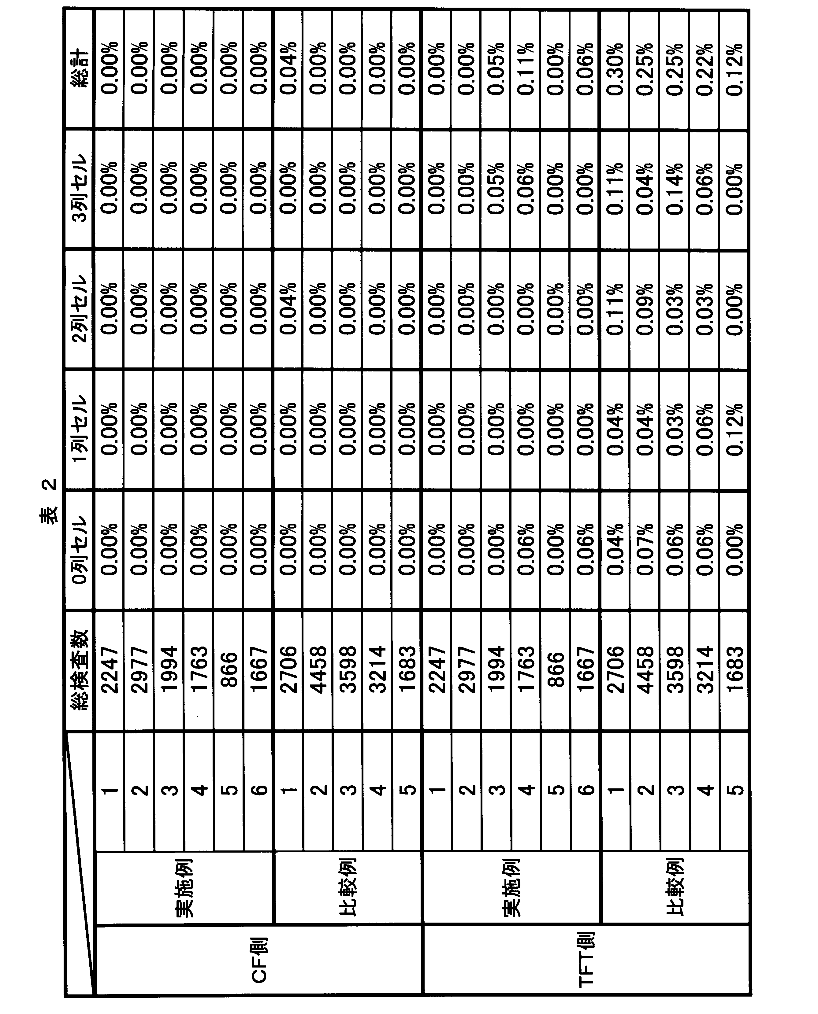
表2の実施例及び比較例の数字は、TFT基板30及びCF基板31の外側に偏光板を貼り付けて表示パネル3を製造したバッチ群(第1バッチ群、第2バッチ群…)を示している。
表2中の0列セル、1列セル、2列セル、3列セルは、マザーガラスから各表示パネル3のユニットを切り出すときの、セルの列である(図5A及び図5B参照)。
表2より、実施例の製造方法により異物の発生が抑制されていること、特に内側の三層構造の基板当接部8及び基板支持部9が当接する1列セル、2列セルにおいては異物の発生が皆無であることが分かる。0列セル、3列セルにおいては、各3本の基板当接部8及び基板支持部9のうち、各1本が第2被覆部83,93を有しない2層構造であるので、異物の発生が生じているが、他の2本が実施例の構成である効果により、比較例より異物の発生率が減じている。
以上より、本発明の表示パネルの製造方法により、基板表面において異物の発生が抑制され、不良率が低減することが確認された。
表2中の0列セル、1列セル、2列セル、3列セルは、マザーガラスから各表示パネル3のユニットを切り出すときの、セルの列である(図5A及び図5B参照)。
表2より、実施例の製造方法により異物の発生が抑制されていること、特に内側の三層構造の基板当接部8及び基板支持部9が当接する1列セル、2列セルにおいては異物の発生が皆無であることが分かる。0列セル、3列セルにおいては、各3本の基板当接部8及び基板支持部9のうち、各1本が第2被覆部83,93を有しない2層構造であるので、異物の発生が生じているが、他の2本が実施例の構成である効果により、比較例より異物の発生率が減じている。
以上より、本発明の表示パネルの製造方法により、基板表面において異物の発生が抑制され、不良率が低減することが確認された。
今回開示された前記実施の形態1~3は、全ての点で例示であって、制限的なものではないと考えるべきである。本発明の範囲は、上述した意味ではなく、請求の範囲と均等の意味及び請求の範囲内での全ての変更が含まれることが意図される。
例えば、基板当接部8、基板支持部9、エアシリンダ73等の数は、実施の形態の1~3で説明した数には限定されない。芯部81,91の形状も実施の形態の1~3で説明した形状に限定されず、四角形状、五角形状であってもよい。
例えば、基板当接部8、基板支持部9、エアシリンダ73等の数は、実施の形態の1~3で説明した数には限定されない。芯部81,91の形状も実施の形態の1~3で説明した形状に限定されず、四角形状、五角形状であってもよい。
また、基板当接部8、基板支持部9は三層構造である場合には限定されず、芯部の表面を一の被覆部で覆うものであってもよい。該被覆部は、耐熱性、静止摩擦係数、静止摩擦力が上述の条件を満たすとともに、離型性が良好であり、貼合基板に跡が付かない材料を用いることが好ましい。
そして、表示パネル3を製造する場合、CF基板31とTFT基板30を貼り合わせた後、液晶材料を注入することにしてもよい。
さらに、反転装置7は、表示パネル3を製造するときに用いる場合に限定されない。
そして、表示パネル3を製造する場合、CF基板31とTFT基板30を貼り合わせた後、液晶材料を注入することにしてもよい。
さらに、反転装置7は、表示パネル3を製造するときに用いる場合に限定されない。
1 TV受信機
2 表示モジュール
3 表示パネル
30 TFT基板
31 CF基板
32 液晶層
33 シール部材
4 前キャビネット
5 後キャビネット
7 反転装置
71 本体
72 軸部支持部
73 エアシリンダ
74 軸部
75 モータ(反転部)
76 ずれ防止部
8 基板当接部(挟持部材)
80 軸部
81、91 芯部
82、84、92、94 第1被覆部
83、93 第2被覆部(耐熱層)
9 基板支持部(挟持部材)
2 表示モジュール
3 表示パネル
30 TFT基板
31 CF基板
32 液晶層
33 シール部材
4 前キャビネット
5 後キャビネット
7 反転装置
71 本体
72 軸部支持部
73 エアシリンダ
74 軸部
75 モータ(反転部)
76 ずれ防止部
8 基板当接部(挟持部材)
80 軸部
81、91 芯部
82、84、92、94 第1被覆部
83、93 第2被覆部(耐熱層)
9 基板支持部(挟持部材)
Claims (11)
- 反転後に所定温度に加熱され、スペーサにより所定の間隔を保持して対向する基板対を夫々の軸心が平行である状態で挟持する挟持部材対と、該挟持部材対に挟持された前記基板対を反転させる反転部とを備える反転装置において、
前記挟持部材は、対向する側に夫々耐熱温度が前記所定温度以上である耐熱層を有することを特徴とする反転装置。 - 前記耐熱層の前記基板対に対する静止摩擦係数は0.3以上であることを特徴とする請求項1に記載の反転装置。
- 前記基板対を挟持した状態での、前記基板対に対する前記耐熱層の静止摩擦力は、9.81×(前記基板対の質量[kg])[N]より大きいことを特徴とする請求項1又は2に記載の反転装置。
- 前記耐熱層は、ガラス繊維又は炭素繊維を有することを特徴とする請求項1から3までのいずれか1項に記載の反転装置。
- 前記耐熱層は、ポリテトラフルオロエチレンを含浸させたガラス繊維、ポリイミド、ナイロン、アルミニウム、ステンレス鋼からなる群から選択される材料を含むことを特徴とする請求項1から4までのいずれか1項に記載の反転装置。
- 前記挟持部材は、金属からなる芯材に前記耐熱層を設けてなることを特徴とする請求項1から5までのいずれか1項に記載の反転装置。
- 前記芯材と前記耐熱層との間に、ポリオレフィン又はエラストマーを含む中間層を有することを特徴とする請求項6に記載の反転装置。
- 前記耐熱層は帯電防止処理を施してある、又は導電性を有することを特徴とする請求項1から7までのいずれか1項に記載の反転装置。
- 前記基板対の端面に当接して、該基板対のずれ落ちを防止するずれ防止部を備えることを特徴とする請求項1から8までのいずれか1項に記載の反転装置。
- 一の矩形状の基板の平面に枠状のシール材を配した後、他の矩形状の基板を貼り合わせる基板貼り合わせ工程、貼り合わせた一対の基板を反転する基板反転工程、及び該一対の基板を所定温度以上に加熱する加熱工程を有する液晶表示パネルの製造方法において、
前記基板反転工程は、請求項1から9までのいずれか1項に記載の反転装置を用いて、前記一対の基板を反転することを特徴とする液晶表示パネルの製造方法。 - 前記基板貼り合わせ工程と前記加熱工程との間に、前記一対の基板に紫外線を照射する工程、及び前記一対の基板を反転する第2の基板反転工程を有し、
前記第2の基板反転工程は、前記反転装置を用いて、前記一対の基板を反転することを特徴とする請求項10に記載の液晶表示パネルの製造方法。
Priority Applications (4)
| Application Number | Priority Date | Filing Date | Title |
|---|---|---|---|
| JP2016571583A JP6420852B2 (ja) | 2015-01-28 | 2015-01-28 | 反転装置、及び液晶表示パネルの製造方法 |
| PCT/JP2015/052392 WO2016121037A1 (ja) | 2015-01-28 | 2015-01-28 | 反転装置、及び液晶表示パネルの製造方法 |
| CN201580074918.3A CN107407830B (zh) | 2015-01-28 | 2015-01-28 | 翻转装置和液晶显示面板的制造方法 |
| US15/661,797 US10254572B2 (en) | 2015-01-28 | 2017-07-27 | Inverting device and method for manufacturing liquid crystal display panel |
Applications Claiming Priority (1)
| Application Number | Priority Date | Filing Date | Title |
|---|---|---|---|
| PCT/JP2015/052392 WO2016121037A1 (ja) | 2015-01-28 | 2015-01-28 | 反転装置、及び液晶表示パネルの製造方法 |
Related Child Applications (1)
| Application Number | Title | Priority Date | Filing Date |
|---|---|---|---|
| US15/661,797 Continuation-In-Part US10254572B2 (en) | 2015-01-28 | 2017-07-27 | Inverting device and method for manufacturing liquid crystal display panel |
Publications (1)
| Publication Number | Publication Date |
|---|---|
| WO2016121037A1 true WO2016121037A1 (ja) | 2016-08-04 |
Family
ID=56542691
Family Applications (1)
| Application Number | Title | Priority Date | Filing Date |
|---|---|---|---|
| PCT/JP2015/052392 Ceased WO2016121037A1 (ja) | 2015-01-28 | 2015-01-28 | 反転装置、及び液晶表示パネルの製造方法 |
Country Status (4)
| Country | Link |
|---|---|
| US (1) | US10254572B2 (ja) |
| JP (1) | JP6420852B2 (ja) |
| CN (1) | CN107407830B (ja) |
| WO (1) | WO2016121037A1 (ja) |
Families Citing this family (2)
| Publication number | Priority date | Publication date | Assignee | Title |
|---|---|---|---|---|
| CN114195376A (zh) * | 2022-01-24 | 2022-03-18 | 湖南飞优特电子科技有限公司 | 一种tft-lcd切割翻版机 |
| TWI794034B (zh) * | 2022-03-04 | 2023-02-21 | 大陸商芯愛科技(南京)有限公司 | 基板結構 |
Citations (4)
| Publication number | Priority date | Publication date | Assignee | Title |
|---|---|---|---|---|
| JP2003233052A (ja) * | 2002-02-04 | 2003-08-22 | Lg Phillips Lcd Co Ltd | 液晶表示素子の製造装置 |
| JP2006227181A (ja) * | 2005-02-16 | 2006-08-31 | Shibaura Mechatronics Corp | 基板反転装置、基板反転方法および基板製造装置 |
| JP2007213092A (ja) * | 2002-05-30 | 2007-08-23 | Lg Phillips Lcd Co Ltd | 液晶表示装置を製造するためのシステム及びこれを用いた液晶表示装置の製造方法 |
| JP2008198882A (ja) * | 2007-02-15 | 2008-08-28 | Dainippon Screen Mfg Co Ltd | 基板処理装置 |
Family Cites Families (10)
| Publication number | Priority date | Publication date | Assignee | Title |
|---|---|---|---|---|
| JP4328472B2 (ja) * | 2001-03-30 | 2009-09-09 | 芝浦メカトロニクス株式会社 | 基板反転装置、及びそれを用いたパネル製造装置 |
| US7102726B2 (en) | 2002-03-15 | 2006-09-05 | Lg. Philips Lcd Co., Ltd. | System for fabricating liquid crystal display and method of fabricating liquid crystal display using the same |
| JP4051500B2 (ja) * | 2002-09-19 | 2008-02-27 | 光洋サーモシステム株式会社 | 熱処理装置用ワーク積載装置 |
| US7238085B2 (en) * | 2003-06-06 | 2007-07-03 | P.C.T. Systems, Inc. | Method and apparatus to process substrates with megasonic energy |
| EP1807157A2 (en) * | 2004-10-22 | 2007-07-18 | Neurologix, Inc. | Use of apoptosis inhibiting compounds in degenerative neurological disorders |
| US7891936B2 (en) * | 2005-03-30 | 2011-02-22 | Brooks Automation, Inc. | High speed substrate aligner apparatus |
| JP2006349913A (ja) | 2005-06-15 | 2006-12-28 | Sharp Corp | 液晶パネルの製造方法 |
| US9050634B2 (en) | 2007-02-15 | 2015-06-09 | SCREEN Holdings Co., Ltd. | Substrate processing apparatus |
| JP2009069705A (ja) * | 2007-09-15 | 2009-04-02 | Citizen Holdings Co Ltd | 液晶表示装置の製造方法 |
| CN101807538B (zh) * | 2010-03-26 | 2011-09-14 | 友达光电股份有限公司 | 基板支撑装置 |
-
2015
- 2015-01-28 JP JP2016571583A patent/JP6420852B2/ja not_active Expired - Fee Related
- 2015-01-28 WO PCT/JP2015/052392 patent/WO2016121037A1/ja not_active Ceased
- 2015-01-28 CN CN201580074918.3A patent/CN107407830B/zh active Active
-
2017
- 2017-07-27 US US15/661,797 patent/US10254572B2/en active Active
Patent Citations (4)
| Publication number | Priority date | Publication date | Assignee | Title |
|---|---|---|---|---|
| JP2003233052A (ja) * | 2002-02-04 | 2003-08-22 | Lg Phillips Lcd Co Ltd | 液晶表示素子の製造装置 |
| JP2007213092A (ja) * | 2002-05-30 | 2007-08-23 | Lg Phillips Lcd Co Ltd | 液晶表示装置を製造するためのシステム及びこれを用いた液晶表示装置の製造方法 |
| JP2006227181A (ja) * | 2005-02-16 | 2006-08-31 | Shibaura Mechatronics Corp | 基板反転装置、基板反転方法および基板製造装置 |
| JP2008198882A (ja) * | 2007-02-15 | 2008-08-28 | Dainippon Screen Mfg Co Ltd | 基板処理装置 |
Also Published As
| Publication number | Publication date |
|---|---|
| CN107407830B (zh) | 2020-11-06 |
| US20170322434A1 (en) | 2017-11-09 |
| JPWO2016121037A1 (ja) | 2017-11-09 |
| US10254572B2 (en) | 2019-04-09 |
| JP6420852B2 (ja) | 2018-11-07 |
| CN107407830A (zh) | 2017-11-28 |
Similar Documents
| Publication | Publication Date | Title |
|---|---|---|
| JP5343862B2 (ja) | ガラス樹脂複合体の製造方法 | |
| TWI477464B (zh) | Glass - Resin composite manufacturing method | |
| KR101827808B1 (ko) | 완전 밀폐 액정 일체형 스크린 및 그 제조 방법 | |
| CN102007524B (zh) | 玻璃层叠体、带支撑体的显示装置用面板及它们的制造方法 | |
| KR101561326B1 (ko) | 편광자 부착 적층체, 지지체 부착 표시 장치용 패널, 표시 장치용 패널, 표시 장치 및 이들의 제조 방법 | |
| KR100949641B1 (ko) | 표시 패널의 제조 방법, 표시 패널의 제조 장치, 및 표시 패널 | |
| JP5134523B2 (ja) | 光学フィルム貼付け装置、光学フィルム貼付け方法、および表示用パネルの製造方法 | |
| TWI467277B (zh) | 軟性液晶顯示器的製造裝置 | |
| EP3264236B1 (en) | Integrated fully-sealed liquid crystal screen and manufacturing process for same | |
| KR101328742B1 (ko) | 편광필름 부착장치 | |
| JP6420852B2 (ja) | 反転装置、及び液晶表示パネルの製造方法 | |
| JP6066055B2 (ja) | 有機el封止装置 | |
| KR101040929B1 (ko) | 유연한 액정 디스플레이, 그의 제조방법 및 그 제조장치 | |
| TWI526313B (zh) | The manufacturing method of the layered body | |
| KR101574217B1 (ko) | 열전사를 통한 인쇄층 형성 방법 | |
| KR100901498B1 (ko) | 기판 제조 장치 및 그 방법 | |
| CN108027581B (zh) | 剥离部件的制造方法和制造装置 | |
| KR100944658B1 (ko) | 휴대폰 표시창 어셈블리의 제조방법 | |
| KR101557523B1 (ko) | 유리기판의 평탄면 형성 장치 및 방법 | |
| KR102156555B1 (ko) | 유리 필름 적층체 | |
| JPH02156220A (ja) | 曲面液晶セルの製造方法 | |
| JP2017067870A (ja) | 剥離部材の製造装置 | |
| JP2005338529A (ja) | 液晶表示基板の配向処理方法および液晶表示基板のマザー基板 | |
| JP2012215757A (ja) | スクリーン、及びスクリーンの製造方法 | |
| JP2017058555A (ja) | 剥離部材の製造方法 |
Legal Events
| Date | Code | Title | Description |
|---|---|---|---|
| 121 | Ep: the epo has been informed by wipo that ep was designated in this application |
Ref document number: 15879934 Country of ref document: EP Kind code of ref document: A1 |
|
| ENP | Entry into the national phase |
Ref document number: 2016571583 Country of ref document: JP Kind code of ref document: A |
|
| NENP | Non-entry into the national phase |
Ref country code: DE |
|
| 122 | Ep: pct application non-entry in european phase |
Ref document number: 15879934 Country of ref document: EP Kind code of ref document: A1 |