WO2016111125A1 - 熱電変換装置及び蓄電システム - Google Patents
熱電変換装置及び蓄電システム Download PDFInfo
- Publication number
- WO2016111125A1 WO2016111125A1 PCT/JP2015/085110 JP2015085110W WO2016111125A1 WO 2016111125 A1 WO2016111125 A1 WO 2016111125A1 JP 2015085110 W JP2015085110 W JP 2015085110W WO 2016111125 A1 WO2016111125 A1 WO 2016111125A1
- Authority
- WO
- WIPO (PCT)
- Prior art keywords
- thermoelectric conversion
- layer
- conversion device
- thermoelectric
- electrode layer
- Prior art date
- Legal status (The legal status is an assumption and is not a legal conclusion. Google has not performed a legal analysis and makes no representation as to the accuracy of the status listed.)
- Ceased
Links
Images

Classifications
-
- H—ELECTRICITY
- H10—SEMICONDUCTOR DEVICES; ELECTRIC SOLID-STATE DEVICES NOT OTHERWISE PROVIDED FOR
- H10N—ELECTRIC SOLID-STATE DEVICES NOT OTHERWISE PROVIDED FOR
- H10N10/00—Thermoelectric devices comprising a junction of dissimilar materials, i.e. devices exhibiting Seebeck or Peltier effects
- H10N10/10—Thermoelectric devices comprising a junction of dissimilar materials, i.e. devices exhibiting Seebeck or Peltier effects operating with only the Peltier or Seebeck effects
- H10N10/17—Thermoelectric devices comprising a junction of dissimilar materials, i.e. devices exhibiting Seebeck or Peltier effects operating with only the Peltier or Seebeck effects characterised by the structure or configuration of the cell or thermocouple forming the device
-
- C—CHEMISTRY; METALLURGY
- C23—COATING METALLIC MATERIAL; COATING MATERIAL WITH METALLIC MATERIAL; CHEMICAL SURFACE TREATMENT; DIFFUSION TREATMENT OF METALLIC MATERIAL; COATING BY VACUUM EVAPORATION, BY SPUTTERING, BY ION IMPLANTATION OR BY CHEMICAL VAPOUR DEPOSITION, IN GENERAL; INHIBITING CORROSION OF METALLIC MATERIAL OR INCRUSTATION IN GENERAL
- C23C—COATING METALLIC MATERIAL; COATING MATERIAL WITH METALLIC MATERIAL; SURFACE TREATMENT OF METALLIC MATERIAL BY DIFFUSION INTO THE SURFACE, BY CHEMICAL CONVERSION OR SUBSTITUTION; COATING BY VACUUM EVAPORATION, BY SPUTTERING, BY ION IMPLANTATION OR BY CHEMICAL VAPOUR DEPOSITION, IN GENERAL
- C23C14/00—Coating by vacuum evaporation, by sputtering or by ion implantation of the coating forming material
- C23C14/06—Coating by vacuum evaporation, by sputtering or by ion implantation of the coating forming material characterised by the coating material
- C23C14/08—Oxides
-
- H—ELECTRICITY
- H02—GENERATION; CONVERSION OR DISTRIBUTION OF ELECTRIC POWER
- H02N—ELECTRIC MACHINES NOT OTHERWISE PROVIDED FOR
- H02N11/00—Generators or motors not provided for elsewhere; Alleged perpetua mobilia obtained by electric or magnetic means
-
- H—ELECTRICITY
- H10—SEMICONDUCTOR DEVICES; ELECTRIC SOLID-STATE DEVICES NOT OTHERWISE PROVIDED FOR
- H10K—ORGANIC ELECTRIC SOLID-STATE DEVICES
- H10K99/00—Subject matter not provided for in other groups of this subclass
-
- H—ELECTRICITY
- H10—SEMICONDUCTOR DEVICES; ELECTRIC SOLID-STATE DEVICES NOT OTHERWISE PROVIDED FOR
- H10N—ELECTRIC SOLID-STATE DEVICES NOT OTHERWISE PROVIDED FOR
- H10N10/00—Thermoelectric devices comprising a junction of dissimilar materials, i.e. devices exhibiting Seebeck or Peltier effects
- H10N10/80—Constructional details
- H10N10/81—Structural details of the junction
-
- H—ELECTRICITY
- H10—SEMICONDUCTOR DEVICES; ELECTRIC SOLID-STATE DEVICES NOT OTHERWISE PROVIDED FOR
- H10N—ELECTRIC SOLID-STATE DEVICES NOT OTHERWISE PROVIDED FOR
- H10N10/00—Thermoelectric devices comprising a junction of dissimilar materials, i.e. devices exhibiting Seebeck or Peltier effects
- H10N10/80—Constructional details
- H10N10/85—Thermoelectric active materials
- H10N10/851—Thermoelectric active materials comprising inorganic compositions
- H10N10/855—Thermoelectric active materials comprising inorganic compositions comprising compounds containing boron, carbon, oxygen or nitrogen
-
- H—ELECTRICITY
- H10—SEMICONDUCTOR DEVICES; ELECTRIC SOLID-STATE DEVICES NOT OTHERWISE PROVIDED FOR
- H10N—ELECTRIC SOLID-STATE DEVICES NOT OTHERWISE PROVIDED FOR
- H10N10/00—Thermoelectric devices comprising a junction of dissimilar materials, i.e. devices exhibiting Seebeck or Peltier effects
- H10N10/80—Constructional details
- H10N10/85—Thermoelectric active materials
- H10N10/856—Thermoelectric active materials comprising organic compositions
Definitions
- the present invention relates to a thermoelectric conversion device and a power storage system in which at least the base material and the thermoelectric conversion layer among the base material, the thermoelectric conversion layer, and the electrode layer are light transmissive.
- thermoelectric material has a characteristic that a potential difference is generated by applying a temperature difference to both ends of the material.
- a potential difference is generated, heat energy is released or absorbed, and the ambient temperature is increased or decreased.
- a technique is disclosed in which a thermoelectric conversion device using a transparent thermoelectric material is energized in a state of being attached to a window glass or the like to function as a cooling device. (See Patent Document 1).
- thermoelectric materials for example, utilizing the characteristics of thermoelectric materials opposite to the technique of Patent Document 1 described above, A technique for regenerating electric energy from heat energy by arranging a thermoelectric conversion device in a place where a temperature difference occurs has been studied.
- An object of the present invention is to provide a thermoelectric conversion device and a power storage system that have light transmittance and can regenerate electric energy from heat energy as a further application of the thermoelectric conversion device.
- thermoelectric conversion device comprising a thermoelectric conversion layer formed from a thermoelectric material and an electrode layer connected to the thermoelectric conversion layer, wherein at least the thermoelectric conversion layer of the thermoelectric conversion layer and the electrode layer is Thermoelectric conversion device having optical transparency.
- Visible light transmittance of 550 nm measured using a spectrophotometer in a direction in which at least the thermoelectric conversion layer intersects the plane of the thermoelectric conversion layer among the thermoelectric conversion layer and the electrode layer is 60% or more.
- thermoelectric conversion device wherein (3) The thermoelectric conversion layer and the electrode layer have a base material disposed on the surface, and the base material is an inorganic material having light permeability or an organic material having light permeability ( The thermoelectric conversion apparatus as described in 1) or (2). (4) The thermoelectric conversion device according to any one of (1) to (3), wherein the thermoelectric material is an n-type thermoelectric material. (5) The thermoelectric conversion device according to any one of (1) to (3), wherein the thermoelectric material is a p-type thermoelectric material.
- the thermoelectric conversion layer includes an n-type thermoelectric conversion layer formed from an n-type thermoelectric material and a p-type thermoelectric conversion layer formed from a p-type thermoelectric material, and the n-type thermoelectric conversion layer and the p-type thermoelectric
- the ratio of the area of the region excluding the region where the electrode layer is formed to the flat area of the thermoelectric conversion device is 1% or more and 99% or less, according to any one of (1) to (6) Thermoelectric converter.
- thermoelectric conversion device and a power storage system that are light transmissive and capable of regenerating electrical energy from thermal energy.
- FIG. 2 is a cross-sectional view taken along line F1-F1 shown in FIG. It is the top view seen from the perpendicular direction to the main surface of thermoelectric conversion device 2 concerning the embodiment of the present invention.
- FIG. 4 is a cross-sectional view taken along line F3-F3 shown in FIG. It is a schematic diagram explaining an example of the fine structure of the electrode layer of the thermoelectric conversion apparatus which concerns on this embodiment. It is a schematic diagram explaining an example of the fine structure of the electrode layer of the thermoelectric conversion apparatus which concerns on this embodiment.
- thermoelectric conversion device is a thermoelectric conversion device including a thermoelectric conversion layer formed from a thermoelectric material and an electrode layer connected to the thermoelectric conversion layer, the thermoelectric conversion layer and the electrode At least the thermoelectric conversion layer of the layers has optical transparency.
- thermoelectric conversion devices 1 and 2 are described in detail with reference to the drawings.
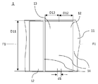
- FIG. 1 is a plan view seen from a direction perpendicular to the main surface of the thermoelectric conversion device 1 formed in a sheet shape
- FIG. 2 is a cross-sectional view taken along line F1-F1 shown in FIG.
- the thermoelectric conversion device 1 includes a base material 11, a thermoelectric conversion layer 12 (p-type semiconductor layer) and a thermoelectric conversion layer 13 (n-type thermoelectric conversion layer) which are disposed on the surface of the base material 11 and formed from a thermoelectric material. ) And an electrode layer 14 connected to the thermoelectric conversion layers 12 and 13.
- the thermoelectric conversion device 1 at least the base material 11 and the thermoelectric conversion layers 12 and 13 among the base material 11, the thermoelectric conversion layers 12 and 13, and the electrode layer 14 have light transmittance. Each component will be described in detail later.
- thermoelectric conversion device 2 shown in FIGS. 3 and 4 is different from the thermoelectric conversion device 1 in the configuration of the thermoelectric conversion layer. It has a so-called single leg type structure using one type of thermoelectric conversion layer selected from a p-type thermoelectric conversion layer and an n-type thermoelectric conversion layer.
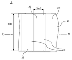
- 3 is a plan view of the thermoelectric conversion device 2 formed in a sheet shape as viewed from the direction perpendicular to the main surface
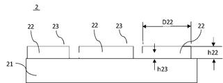
- FIG. 4 is a cross-sectional view taken along line F3-F3 shown in FIG.
- the thermoelectric conversion device 2 includes a base material 21, a thermoelectric conversion layer 22, and an electrode layer 23 connected to the thermoelectric conversion layer 22. In the thermoelectric conversion device 2, at least the base material 21 and the thermoelectric conversion layer 22 among the base material 21, the thermoelectric conversion layer 22, and the electrode layer 23 have light transmittance. Each component will be described in detail later.
- thermoelectric conversion layer of the thermoelectric conversion layer and the electrode layer has a visible light transmittance of 550 nm measured using a spectrophotometer in the direction intersecting the plane of the base material of 60%.
- the base materials 11 and 21 may be omitted. That is, the thermoelectric conversion layer and the electrode layer may be directly formed on, for example, a display surface of an electronic device such as an information processing terminal, a window glass of a building, or a glass for a car.
- the thickness of the thermoelectric conversion devices 1 and 2 is preferably 0.2 ⁇ m or more and 6000 ⁇ m or less.
- the thermoelectric conversion device 1 can be formed into a sheet having a desired area by connecting a plurality of units with electrodes. The same applies to the thermoelectric converter 2. Although not shown in FIGS. 1 to 4, the electrode layer 14 of the thermoelectric conversion device 1 is connected to an electrode layer for taking out a thermoelectric power, and the thermoelectric power is transferred from the thermoelectric conversion device 1. It can be taken out and stored in a power storage device or the like, or used as a power source for the device.
- thermoelectric conversion layer 22 and an electrode layer 23 are disposed on the surfaces of the base materials 11 and 21 according to the present embodiment.
- the base materials 11 and 21 are not particularly limited as long as they are light-transmitting inorganic materials or light-transmitting organic materials and have sufficient strength.
- glass materials such as soda lime glass, borosilicate glass, quartz glass, borosilicate glass, alkali-free glass, blue plate glass, white plate glass, aluminosilicate glass and calcium fluoride glass, polyimide, polyamide, polyamide Imide, polyphenylene ether, polyether ketone, polyether ether ketone, polyolefin, polyester, polycarbonate, polysulfone, polyether sulfone, polyphenylene sulfide, polyarylate, acrylic resin, cycloolefin polymer, aromatic polymer, polyurethane Examples thereof include polymers.
- polyester since it is excellent in transparency and has versatility, polyester, polyamide or cycloolefin polymer is preferable, and polyester or cycloolefin polymer is more preferable.
- polyester include polyethylene terephthalate, polybutylene terephthalate, polyethylene naphthalate, and polyarylate.
- polyamide include wholly aromatic polyamide, nylon 6, nylon 66, nylon copolymer, and the like.
- cycloolefin polymers include norbornene polymers, monocyclic olefin polymers, cyclic conjugated diene polymers, vinyl alicyclic hydrocarbon polymers, and hydrides thereof.
- Apel registered trademark, ethylene-cycloolefin copolymer manufactured by Mitsui Chemicals
- Arton registered trademark, norbornene polymer manufactured by JSR
- Zeonore registered trademark, manufactured by Nippon Zeon Co., Ltd.
- Norbornene polymer norbornene polymer
- polyesters such as polyethylene terephthalate, polybutylene terephthalate, polyethylene naphthalate, and polyarylate are preferable, and polyethylene terephthalate is more preferable.
- the substrate may contain various additives such as an antioxidant, a flame retardant, and a lubricant as long as transparency and the like are not impaired.
- the thickness of the substrate is preferably 0.1 ⁇ m or more and 5000 ⁇ m or less. When the thickness of the substrate is within this range, a thermoelectric conversion device having excellent transparency can be easily obtained.
- the total light transmittance (measured in accordance with JIS K7361-1) of the substrate is preferably 70% or more, more preferably 70 to 100%, and still more preferably 80 to 95%.
- the haze value of the substrate is preferably 10% or less, more preferably 1 to 10%.
- the visible light transmittance (transmittance at 550 nm) of the substrate is preferably 60% or more, more preferably 80% or more, still more preferably 85% or more and 99% or less, and particularly preferably. 90% or more and 99% or less.
- the refractive index of the substrate varies depending on the material and the presence or absence of stretching, but is usually in the range of 1.45 to 1.75, preferably 1.6 to 1.75 from the viewpoint of transparency.
- thermoelectric conversion layers 12, 13 and 22 are made of a thermoelectric material having a high Seebeck effect and light transmittance.
- thermoelectric materials include inorganic materials and organic materials, and examples of inorganic materials include metals, alloys, metal oxides, electrically conductive compounds, and mixtures thereof.
- tin oxide antimony-doped tin oxide (ATO); fluorine-doped tin oxide (FTO), zinc oxide, gallium-doped zinc oxide (GZO), aluminum-doped zinc oxide (AZO) , Indium oxide, indium tin oxide (ITO), indium zinc oxide (IZO), and other conductive metal oxides; gold, silver, chromium, nickel, and other metals; a mixture of these metals and conductive metal oxides; Inorganic conductive materials such as copper halide and copper sulfide; organic conductive materials such as polyaniline, polythiophene and polypyrrole; and the like.
- conductive metal oxides are preferable from the viewpoint of conductivity.
- Zinc oxide, zinc oxide doped with gallium (GZO), and aluminum are used to reduce the amount of rare metal used and to design an environment-friendly product.
- Zinc oxide-based conductive materials such as doped zinc oxide (AZO) and zinc indium oxide (IZO) are more preferable, and in view of durability and material cost, zinc oxide doped with gallium (GZO) is more preferable and conductive.
- zinc oxide to which digallium trioxide is added in an amount of 1 to 10% is particularly preferable.
- the thermoelectric conversion layers 12, 13 and 22 may be formed by laminating a plurality of layers made of the above-described materials.
- thermoelectric conversion layer examples include those having a Seebeck effect and light transmittance.
- organic polymer compounds include polyanilines and polypyrroles, which are conductive polymers having conductivity by ⁇ -electron conjugation, because they are excellent in dispersibility, easy to form a coating film, and highly transparent.
- at least one selected from polythiophenes and their derivatives is preferably used.
- Polyanilines are high molecular weight compounds of compounds in which the 2-position, 3-position or N-position of aniline is substituted with an alkyl group having 1 to 18 carbon atoms, an alkoxy group, an aryl group, a sulfonic acid group or the like.
- Methyl aniline poly 3-methyl aniline, poly 2-ethyl aniline, poly 3-ethyl aniline, poly 2-methoxy aniline, poly 3-methoxy aniline, poly 2-ethoxy aniline, poly 3-ethoxy aniline, poly N-methyl aniline Poly N-propyl aniline, poly N-phenyl-1-naphthyl aniline, poly 8-anilino-1-naphthalene sulfonic acid, poly 2-aminobenzene sulfonic acid, poly 7-anilino-4-hydroxy-2-naphthalene sulfonic acid Etc.
- Polypyrroles are high molecular weight compounds of compounds in which 1-position, 3-position or 4-position of pyrrole is substituted with an alkyl group or alkoxy group having 1 to 18 carbon atoms, such as poly 1-methyl pyrrole, poly 3-pyrrole. Examples thereof include methyl pyrrole, poly 1-ethyl pyrrole, poly 3-ethyl pyrrole, poly 1-methoxy pyrrole, 3-methoxy pyrrole, poly 1-ethoxy pyrrole, poly 3-ethoxy pyrrole and the like.
- Polythiophenes are high molecular weight compounds of compounds in which the 3-position or 4-position of thiophene is substituted with an alkyl group or alkoxy group having 1 to 18 carbon atoms, such as poly-3-methylthiophene, poly-3-ethylthiophene, poly And high molecular weight compounds such as 3-methoxythiophene, poly-3-ethoxythiophene, and poly3,4-ethylenedioxythiophene (PEDOT).
- Examples of the derivatives of polyanilines, polypyrroles or polythiophenes include these dopant bodies.
- halide ions such as chloride ion, bromide ion and iodide ion; perchlorate ion; tetrafluoroborate ion; hexafluoroarsenate ion; sulfate ion; nitrate ion; thiocyanate ion; hexafluoride Silicate ion; Phosphate ion such as phosphate ion, phenyl phosphate ion, hexafluorophosphate ion; trifluoroacetate ion; alkylbenzenesulfonate ion such as tosylate ion, ethylbenzenesulfonate ion, dodecylbenzenesulfonate ion; methylsulfone Alkyl sulfonate ions such as acid ions and ethyl sulfonate ions; or poly
- polyacrylate ions such as polystyrene sulfonate ion (PSS) and poly (2-acrylamido-2-methylpropane sulfonate) ion are preferred, and polystyrene sulfonate ion (PSS) which is a water-soluble and strongly acidic polymer is more preferred.
- PSS polystyrene sulfonate ion
- polypyrrole or polythiophene a derivative of polythiophene is preferable, and among them, a mixture of poly (3,4-ethylene oxide thiophene) and polystyrenesulfonate ion as a dopant (hereinafter referred to as “PEDOT: May be described as “PSS”).
- PES polystyrenesulfonate ion as a dopant
- thermoelectric conversion layer made of an n-type thermoelectric material a single-leg type thermoelectric conversion layer made only of n-type GZO can be used.
- thermoelectric conversion layer made of a p-type thermoelectric material a single-leg type thermoelectric conversion layer made only of PEDOT: PSS can be used.
- the thermoelectric conversion layer includes an n-type thermoelectric conversion layer formed from an n-type thermoelectric material and a p-type thermoelectric conversion layer formed from a p-type thermoelectric material, and the n-type thermoelectric conversion A pn junction type in which a layer and the p-type thermoelectric conversion layer are connected by an electrode layer is preferable.
- the pn junction type which combined PEDOT: PSS and GZO is preferable.
- the thermoelectric conversion layer may be a single layer made of the above-described material, or may have a structure in which two or more layers made of different types of materials among the above-described materials are stacked.
- the combined thickness of the thermoelectric conversion layer and the electrode layer described below is preferably 0.1 ⁇ m or more and 1000 ⁇ m or less, and more preferably 0.1 ⁇ m or more and 10 ⁇ m or less. If it is the said range, a total light transmittance will be high and favorable transparency will be obtained. Further, the total light transmittance of the thermoelectric conversion layer alone is preferably 50% or more, more preferably 60% or more and 90% or less, and further preferably 70% or more and 90% or less.
- the haze value of the thermoelectric conversion layer alone is preferably 10% or less, more preferably 1% or more and 5% or less. When the total light transmittance and haze value of the thermoelectric conversion layer are within these ranges, a thermoelectric conversion layer having excellent transparency can be easily obtained.
- the visible light transmittance (550 nm transmittance) of the thermoelectric conversion layer alone is preferably 60% or more, more preferably 65% or more and 90% or less, and further preferably 70% or more and 90% or less. .
- the electric conductivity of the thermoelectric conversion layer is preferably 100 S / cm or more and 1500 S / cm or less, more preferably 400 S, from the viewpoint of increasing the output voltage regardless of whether the thermoelectric conversion layer is n-type or p-type. / Cm or more and 1300 S / cm or less.
- the thermal conductivity of the thermoelectric conversion layer is preferably 0.1 or more and 100 or less from the viewpoint of increasing the output voltage regardless of whether the thermoelectric conversion layer is n-type or p-type, and 0.1 W / m ⁇ K or more and 50 W or more. / M ⁇ K or less is more preferable, and 0.1 W / m ⁇ K or more and 10 W / m ⁇ K or less is more preferable.
- the electrode layer 14 is a ratio of the area of the region excluding the region where the electrode layer is formed to the plane area of the thermoelectric conversion device, considering the light transmittance of the thermoelectric conversion device 1. Is preferably 1% or more and 99% or less. From the viewpoint of improving the light transmittance of the thermoelectric conversion device 1, the electrode layer 14 is more preferably formed from a material having light transmittance. Since the electrode layer 23 in the thermoelectric conversion device 2 can be similarly defined, the electrode layer 14 used in the thermoelectric conversion device 1 will be described below.
- the shape of the electrode layer 14 viewed from the direction perpendicular to the main surface of the thermoelectric conversion device 1 has a fine structure such as a metal grid pattern used as an electromagnetic wave shielding film of a plasma display.
- the electrode layer 14 is formed of a material that does not transmit light, the electrode layer 14 has a large number or wide opening so as not to interfere with the light transmission of the thermoelectric conversion device 1. Those are preferred.
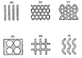
- the shape of the opening of the electrode layer 14 viewed from the direction perpendicular to the main surface of the thermoelectric conversion device 1 is a stripe shape, a straight shape, a curved shape, a wavy shape such as a sine curve, a mesh shape such as a lattice, or a polygonal mesh shape. Shape, circular mesh shape, elliptical mesh shape, or indefinite shape. For example, as shown in (a) to (f) of FIG.
- the thickness of the electrode layer 14 is preferably 0.1 ⁇ m or more and 1000 ⁇ m or less, more preferably 1 ⁇ m or more and 500 ⁇ m or less, and further preferably 5 ⁇ m or more and 100 ⁇ m or less.
- the aperture ratio of the electrode layer 14 is preferably 1% or more and 99% or less, more preferably 90% or more and 99% or less, and still more preferably 95% or more and 99% from the viewpoint of light transmittance of the thermoelectric conversion device 1. % Or less.
- the aperture ratio is the ratio of the area of the region excluding the region where the electrode layer 14 is formed to the plane area of the thermoelectric conversion device 1.
- the line width of the electrode layer 14 is preferably 10 nm to 1000 ⁇ m, more preferably 10 to 500 ⁇ m. If the line width is in the above range, good light transmittance can be obtained without impairing conductivity.
- the material for forming the electrode layer 14 is at least one selected from gold, silver, copper, and platinum, or an alloy containing the one. Since these materials have a low ionization tendency among metals, they have high corrosion resistance and are suitable.
- the alloy is not particularly limited as long as it is an alloy mainly composed of at least one selected from gold, silver, copper, and platinum, or one of them. Examples of these alloys include bronze, phosphor bronze, brass, white bronze, monel, and the like, which can be appropriately selected. In particular, an alloy mainly composed of copper is preferably used because it has excellent conductivity and good workability.
- the electrode layer 14 may be a single layer or a multilayer structure.
- the electrode layer preferably has a multi-layer structure from the viewpoint that the corrosion resistance can be improved while maintaining conductivity.
- the multilayer structure may be a multilayer structure in which layers made of the same kind of material are laminated, or a multilayer structure in which layers made of at least two kinds of materials are laminated. From the viewpoint that corrosion resistance can be improved, a multilayer structure in which layers made of at least two kinds of materials are laminated is preferable.
- a pattern layer made of an alloy material containing at least one selected from gold, silver, copper, and platinum or an alloy material is formed on the substrate 11, and the pattern layer is formed on the pattern layer. It is preferable to laminate a pattern layer made of a material having high corrosion resistance.
- the multilayer structure is more preferably a two-layer structure in which layers of different materials are stacked.
- a multilayer structure for example, when a silver pattern layer is first formed and then a copper pattern layer having a higher corrosion resistance than silver is formed thereon, a high resistance of silver is maintained. Corrosivity is improved.
- thermoelectric conversion device Next, a method for manufacturing a thermoelectric conversion device will be described.
- the electrode layer 14 is formed on the surface of the substrate 11 using the thermoelectric material described above. After the electrode layer 14 is formed, the thermoelectric conversion layers 12 and 13 are formed. Furthermore, the electrode layer 14 is formed again.
- Examples of a method for forming a thermoelectric conversion layer using an inorganic material include a vapor deposition method, a sputtering method, an ion plating method, a thermal CVD method, a plasma CVD method, and the like. Among these, in the present invention, the sputtering method is preferable because the conductor layer can be easily formed.
- the sputtering method introduces a discharge gas (such as argon) into a vacuum chamber, applies a high-frequency voltage or a direct current voltage between the target and the substrate to turn the discharge gas into plasma, and collides the plasma with the target material.
- a discharge gas such as argon
- a target made of a material for forming the thermoelectric conversion layer is used as the target.
- thermoelectric conversion layers using organic materials include various coating methods such as dip coating, spin coating, spray coating, gravure coating, die coating, and doctor blade, and wet processes such as electrochemical deposition. Are selected as appropriate.
- an organic polymer compound aqueous dispersion or solution (coating solution) is provided on the substrate 11 by various coating methods such as dip coating, spin coating, spray coating, gravure coating, die coating, and doctor blade.
- the electrode layer 14 can be applied.
- a method of providing the electrode layer 14 on the base material 11 for example, a method of attaching the electrode layer 14 using an adhesive, a conductive paste or the like, or a pattern is not formed on the base material 11 ( After forming the electrode layer (which has no opening), a method of processing the fine structure by various known mechanical treatments or chemical treatments, and the conductive metal pattern directly on the substrate 11 by an inkjet method, a screen printing method or the like And the like.
- dry deposition such as PVD (physical vapor deposition) such as vacuum deposition, sputtering, ion plating, or CVD (chemical vapor deposition) such as thermal CVD, atomic layer deposition (ALD), etc.
- CVD chemical vapor deposition
- Various coating methods such as dip coating, spin coating, spray coating, gravure coating, die coating, doctor blade, etc., wet processes such as electrochemical deposition, silver salt method, etc. It is appropriately selected depending on.
- Various known mechanical treatments, chemical treatments, and the like can be applied, and depending on the material and the fine structure putter among the above methods. It is selected appropriately.
- a primer layer such as a conventionally known acrylic resin or polyurethane resin having light transmittance may be interposed.
- the power storage system includes a power storage device that stores electricity in addition to the thermoelectric conversion device. You may have the control circuit which controls the electrical storage operation
- the power storage device includes a secondary battery, a capacitor, and the like.
- the secondary battery may be any battery that can store electricity, for example, lithium battery, lithium polymer battery, lithium ion battery, nickel metal hydride battery, nickel-cadmium battery, organic radical battery, lead storage battery, air secondary battery, nickel zinc battery, silver zinc A battery etc. are mentioned.
- the capacitor include an electric double layer capacitor and a lithium ion capacitor.
- thermoelectric performance of the thermoelectric converter described later was evaluated by the following method.
- ⁇ Electric conductivity and Seebeck coefficient> The electric conductivity and Seebeck coefficient of the thermoelectric conversion layer were measured using a thermoelectric property evaluation apparatus (“ZEM-3” manufactured by ULVAC-RIKO Inc.).
- ⁇ Thermal conductivity> The thermal conductivity of the thermoelectric conversion layer was measured by the 3 ⁇ method.
- a cooling device combining a chiller (manufactured by As One Co., Ltd., “LTCi-150H”) and a water-cooled cooler (manufactured by Takagi Seisakusho Co., Ltd., “P-200S”), and a hot plate (manufactured by As One Co., Ltd., “THI-1000”
- the temperature gradient was formed using the “)”, that is, the hot plate heated to 50 ° C. was brought into close contact with the substrate side of the thermoelectric conversion device, and set to 0 ° C. on the opposite side of the substrate of the thermoelectric conversion device.
- thermoelectric converter A temperature gradient was applied to the thermoelectric converter by bringing the chiller into contact, and in this state, the temperature of the base material in contact with the hot plate and the temperature of the upper surface of the electrode layer in contact with the chiller were compared with the K-type thermocouple and data. Measured with a measuring device combined with a logger (Edo Electric Co., Ltd., “Cadak 3”), a temperature difference was calculated, and a digital multimeter (Hioki Electric Co., Ltd., “DT42”) was calculated. 82 "), the output voltage of the thermoelectric converter was measured.
- thermoelectric converter ⁇ Light transmittance (% T 550 )> Using a spectrophotometer (manufactured by Shimadzu Corporation, “UV3601”), the visible light transmittance (transmittance at 550 nm) of the thermoelectric converter was measured in accordance with JIS K7361-1.
- thermoelectric conversion device was produced as follows. ⁇ Example 1> On the surface of a glass substrate (CORNING Co., Ltd., “Eagle XG”, thickness 0.7 mm), a silver paste is printed in a stripe pattern in a predetermined pattern using a screen printing method, and then at 150 ° C. for 30 minutes. It dried and formed the light transmissive electrode layer of the predetermined pattern.
- a glass substrate CORNING Co., Ltd., “Eagle XG”, thickness 0.7 mm
- a silver paste is printed in a stripe pattern in a predetermined pattern using a screen printing method, and then at 150 ° C. for 30 minutes. It dried and formed the light transmissive electrode layer of the predetermined pattern.
- PEDOT PSS (manufactured by Agfa Material Co., Ltd., “S-305”, thermal conductivity 0.3 W / m ⁇ K), which is an organic p-type thermoelectric material, was applied to an inkjet printing apparatus (manufactured by MicroJet Corporation, A p-type thermoelectric conversion layer was formed using “NanoPrinter-300”). After formation, it was dried at 150 ° C. in the atmosphere. Subsequently, a transparent n-type thermoelectric conversion layer was formed by sputtering using gallium-doped zinc oxide (GZO), which is an n-type thermoelectric material.
- GZO gallium-doped zinc oxide
- thermoelectric conversion device a of the type shown in FIG. 2 was produced.
- the thickness (h12) of the p-type thermoelectric conversion layer 12 and the thickness (h13) of the n-type thermoelectric conversion layer were set to 0.2 ⁇ m, and the thickness (h14) of the electrode layer was set to 0.1 ⁇ m.
- the specimen was heated by the method described above, and the temperature difference generated in the thermoelectric conversion device a was measured. Further, the obtained potential difference and the light transmittance of the thermoelectric converter were measured. The results are shown in Table 1 together with the electrical conductivity and thermal conductivity of the p-type thermoelectric conversion layer and the n-type thermoelectric conversion layer used.
- Example 2 On the surface of a glass substrate (CORNING Co., Ltd., “Eagle XG”, thickness 0.7 mm), a silver paste is printed in a predetermined pattern using a screen printing method, and then dried at 150 ° C. for 30 minutes. A light transmissive electrode was formed. Subsequently, PEDOT: PSS (manufactured by Agfa Material Co., Ltd., “S-305”, thermal conductivity 0.3 W / m ⁇ K), which is an organic p-type thermoelectric material, was applied to an inkjet printing apparatus (manufactured by MicroJet Corporation, A p-type thermoelectric conversion layer was formed using “NanoPrinter-300”).
- PEDOT: PSS manufactured by Agfa Material Co., Ltd., “S-305”, thermal conductivity 0.3 W / m ⁇ K
- thermoelectric conversion layer was printed in a predetermined pattern in the same manner as described above, and then dried at 150 ° C. for 30 minutes to form a light-transmitting electrode having a predetermined pattern.
- a conversion device b was produced.
- the thickness (h22) of the thermoelectric conversion layer was set to 0.2 ⁇ m, and the thickness (h23) of the electrode layer was set to 0.1 ⁇ m.
- thermoelectric conversion layer The specimen was heated by the method described above, and the temperature difference generated in the thermoelectric converter b was measured. Further, the obtained potential difference and the light transmittance of the thermoelectric converter were measured. The results are shown in Table 1 together with the electrical conductivity and thermal conductivity of the p-type thermoelectric conversion layer used.
- thermoelectric conversion layer In the same manner as in Example 1, after forming a light transmissive electrode layer on a glass substrate, a transparent n-type thermoelectric conversion layer was formed by sputtering using gallium-doped zinc oxide (GZO). After the formation of the thermoelectric conversion layer, a light transmissive electrode layer having a predetermined pattern was formed in the same manner as in Example 1, and a thermoelectric conversion device c of the type shown in FIGS. 3 and 4 was produced. The dimensions of the thermoelectric conversion layer and the electrode layer in the thermoelectric conversion device c were the same as those of the thermoelectric conversion device b. The specimen was heated by the method described above, and the temperature difference generated in the thermoelectric conversion device c was measured. Further, the obtained potential difference and the light transmittance of the thermoelectric converter were measured. The results are shown in Table 1 together with the electrical conductivity and thermal conductivity of the n-type thermoelectric conversion layer used.
- GZO gallium-doped zinc oxide
- Example 4 In the same manner as in Example 1, after forming a light transmissive electrode layer having a mesh structure on a glass substrate, a transparent n-type thermoelectric conversion layer was formed by sputtering using indium tin oxide (ITO). After the formation of the thermoelectric conversion layer, a light transmissive electrode layer having a predetermined pattern was formed in the same manner as in Example 1, and a thermoelectric conversion device d of the type shown in FIGS. 3 and 4 was produced. The dimensions of the thermoelectric conversion layer and the electrode layer in the thermoelectric conversion device d were the same as those of the thermoelectric conversion device b. The specimen was heated by the method described above, and the temperature difference generated in the thermoelectric converter d was measured. Further, the obtained potential difference and the light transmittance of the thermoelectric converter were measured. The results are shown in Table 1 together with the electrical conductivity and thermal conductivity of the n-type thermoelectric conversion layer used.
- ITO indium tin oxide
- thermoelectric conversion device of the present invention has light transmissivity and can regenerate part of the heat energy into electric energy
- the display surface of an electronic device such as an information processing terminal that requires energy saving, It can be placed on window glass, car glass and the like.
- thermoelectric conversion device 11, 21 base material, 12, 13, 22 thermoelectric conversion layer, 14, 23 electrode layer
Landscapes
- Chemical & Material Sciences (AREA)
- Inorganic Chemistry (AREA)
- Chemical Kinetics & Catalysis (AREA)
- Engineering & Computer Science (AREA)
- Materials Engineering (AREA)
- Mechanical Engineering (AREA)
- Metallurgy (AREA)
- Organic Chemistry (AREA)
- Laminated Bodies (AREA)
- Non-Insulated Conductors (AREA)
Abstract
Description
近年、環境への配慮や省エネルギーへの関心の高まりから、熱電材料の上述した特性を生かして、例えば、上述した特許文献1の技術とは反対の熱電材料の特性を利用して、恒常的に温度差が発生する場所に熱電変換デバイスを配置することにより、熱エネルギーから電気エネルギーを回生する技術が検討されている。
(1)熱電材料から形成された熱電変換層と、該熱電変換層に接続された電極層とを備える熱電変換装置であって、該熱電変換層及び該電極層のうち少なくとも該熱電変換層が光透過性を有する熱電変換装置。
(2)前記熱電変換層及び前記電極層のうち少なくとも前記熱電変換層が該熱電変換層の平面に交差する方向において、分光光度計を用いて測定される550nmの可視光透過率が60%以上である前記(1)に記載の熱電変換装置。
(3)前記熱電変換層と前記電極層とが表面に配設された基材を有し、該基材が光透過性を有する無機系材料又は光透過性を有する有機系材料である前記(1)又は(2)に記載の熱電変換装置。
(4)前記熱電材料がn型熱電材料である前記(1)~(3)のいずれかに記載の熱電変換装置。
(5)前記熱電材料がp型熱電材料である前記(1)~(3)のいずれかに記載の熱電変換装置。
(6)前記熱電変換層がn型熱電材料から形成されたn型熱電変換層及びp型熱電材料から形成されたp型熱電変換層を有し、該n型熱電変換層及び該p型熱電変換層が前記電極層によって、接続されている前記(1)~(5)のいずれかに記載の熱電変換装置。
(7)前記熱電変換装置の平面積に対する、前記電極層が形成された領域を除く領域の面積の割合が1%以上99%以下である前記(1)~(6)のいずれかに記載の熱電変換装置。
(8)前記電極層が光透過性を有する前記(1)~(7)のいずれかに記載の熱電変換装置。
(9)前記(1)~(8)のいずれかに記載の熱電変換装置と、電気を蓄電する蓄電装置と、を備え、該熱電変換装置における前記電極層が該蓄電装置に電気的に接続されてなる蓄電システム。
本発明の実施形態に係る熱電変換装置は、熱電材料から形成された熱電変換層と、該熱電変換層に接続された電極層とを備える熱電変換装置であって、該熱電変換層及び該電極層のうち少なくとも該熱電変換層が光透過性を有する。
本発明の実施形態に係る熱電変換装置1,2について、図面を用いて詳細に説明する。図1は、シート状に形成された熱電変換装置1の主面に垂直方向からみた平面図であり、図2は、図1に示すF1-F1線における断面図である。
熱電変換装置1は、基材11と、該基材11の表面に配設されており熱電材料から形成された熱電変換層12(p型半導体層)及び熱電変換層13(n型熱電変換層)と、該熱電変換層12,13に接続された電極層14とを備えたpn接合型の構造を有する。熱電変換装置1は、基材11、熱電変換層12,13、及び電極層14のうち少なくとも基材11及び熱電変換層12,13が光透過性を有する。各構成要件は、後段にて詳細に説明する。
熱電変換装置2は、基材21と、熱電変換層22と、該熱電変換層22に接続された電極層23とを備える。熱電変換装置2は、基材21、熱電変換層22及び電極層23のうち少なくとも基材21及び熱電変換層22が光透過性を有する。各構成要件は、後段にて詳細に説明する。
なお、熱電変換装置1,2において、基材11,21は、無くてもよい。すなわち、熱電変換層及び電極層が、例えば、情報処理端末等の電子機器の表示面、建物の窓ガラス、車用ガラス等に直接形成されていてもよい。
光透過性の観点から、熱電変換装置1,2の厚みは、0.2μm以上6000μm以下であることが好ましい。
熱電変換装置1は、複数のユニットを電極によって接続することにより、所望の面積を有するシートにすることができる。熱電変換装置2も同様である。
また、図1~図4には、図示されていないが、熱電変換装置1の電極層14には、熱起電力取出用の電極層が接続されており、熱電変換装置1から熱起電力を取り出し、蓄電装置等に蓄えられるか、デバイスの電源として使用できる。
本実施形態に係る基材11及び21の表面には、熱電変換層22と電極層23とが配設されている。基材11及び21は、光透過性を有する無機系材料又は光透過性を有する有機系材料であって、十分な強度を有するものであれば特に制限されない。
基材の材質としては、ソーダライムガラス、硼珪酸ガラス、石英ガラス、ホウケイ酸ガラス、無アルカリガラス、青板ガラス、白板ガラス、アルミノシリケートガラス及びフッ化カルシウムガラス等のガラス素材、ポリイミド、ポリアミド、ポリアミドイミド、ポリフェニレンエーテル、ポリエーテルケトン、ポリエーテルエーテルケトン、ポリオレフィン、ポリエステル、ポリカーボネート、ポリスルフォン、ポリエーテルスルフォン、ポリフェニレンスルフィド、ポリアリレート、アクリル系樹脂、シクロオレフィン系ポリマー、芳香族系重合体、ポリウレタン系ポリマー等が挙げられる。
ポリエステルとしては、ポリエチレンテレフタレート、ポリブチレンテレフタレート、ポリエチレンナフタレート、ポリアリレート等が挙げられる。
ポリアミドとしては、全芳香族ポリアミド、ナイロン6、ナイロン66、ナイロン共重合体等が挙げられる。
シクロオレフィン系ポリマーとしては、ノルボルネン系重合体、単環の環状オレフィン系重合体、環状共役ジエン系重合体、ビニル脂環式炭化水素重合体、及びこれらの水素化物が挙げられる。その具体例としては、アペル(登録商標、三井化学社製のエチレン-シクロオレフィン共重合体)、アートン(登録商標、JSR社製のノルボルネン系重合体)、ゼオノア(登録商標、日本ゼオン社製のノルボルネン系重合体)等が挙げられる。
基材は、これらの成分の他に、透明性等を損なわない範囲で、酸化防止剤、難燃剤、滑剤等の各種添加剤を含んでもよい。
基材の厚みは、0.1μm以上5000μm以下であることが好ましい。基材の厚みがこの範囲内であることで、透明性に優れる熱電変換装置を容易に得ることができる。
特に、基材の可視光透過率(550nmの透過率)は、好ましくは、60%以上、より好ましくは、80%以上であり、さらに好ましくは、85%以上99%以下であり、特に好ましくは、90%以上99%以下である。また、基材の屈折率は、材質、延伸の有無によって異なるが、透明性の観点から、通常、1.45~1.75、好ましくは1.6~1.75の範囲である。
本実施形態において、熱電変換層12,13及び22は、高いゼーベック効果を有し、かつ光透過性を有する熱電材料から形成されている。
このような熱電材料には、無機系材料及び有機系材料があり、無機系材料としては、金属、合金、金属酸化物、電気伝導性化合物、これらの混合物等が挙げられる。具体的には、酸化スズ、アンチモンをドープした酸化スズ(ATO);フッ素をドープした酸化スズ(FTO)、酸化亜鉛、ガリウムをドープした酸化亜鉛(GZO)、アルミニウムをドープした酸化亜鉛(AZO)、酸化インジウム、酸化インジウムスズ(ITO)、酸化亜鉛インジウム(IZO)、等の導電性金属酸化物;金、銀、クロム、ニッケル等の金属;これら金属と導電性金属酸化物との混合物;ヨウ化銅、硫化銅等の無機導電性物質;ポリアニリン、ポリチオフェン、ポリピロール等の有機導電性材料;等が挙げられる。
ポリアニリン類、ポリピロール類またはポリチオフェン類の誘導体としては、これらのドーパント体等が挙げられる。
上記ポリアニリン類、ポリピロール類またはポリチオフェン類の誘導体としては、ポリチオフェン類の誘導体が好ましく、中でも、ポリ(3,4-エチレンオキサイドチオフェン)と、ドーパントとして、ポリスチレンスルホン酸イオンの混合物(以下、「PEDOT:PSS」と記載することがある)等が好ましい。
さらにまた、本発明の実施形態においては、熱電変換層がn型熱電材料から形成されたn型熱電変換層及びp型熱電材料から形成されたp型熱電変換層を有し、n型熱電変換層及び該p型熱電変換層が電極層によって接続されたpn接合型が好ましい。なかでも、PEDOT:PSSと、GZOとを組み合わせたpn接合型が好ましい。
熱電変換層及び後述する電極層を合わせた厚みは、0.1μm以上1000μm以下であることが好ましく、より好ましくは、0.1μm以上10μm以下である。上記範囲であれば、全光線透過率が高く、良好な透明性が得られる。
また、熱電変換層単独の全光線透過率は、好ましくは50%以上であり、より好ましくは、60%以上90%以下であり、さらに好ましくは、70%以上90%以下である。
熱電変換層単独のヘイズ値は、好ましくは10%以下、より好ましくは、1%以上5%以下である。熱電変換層の全光線透過率やヘイズ値がこれらの範囲内であることで、透明性に優れる熱電変換層を容易に得ることができる。
特に、熱電変換層単独の可視光透過率(550nmの透過率)は、好ましくは、60%以上、より好ましくは65%以上90%以下であり、さらに好ましくは、70%以上90%以下である。
また、熱電変換層の電気伝導率は、熱電変換層がn型又はp型に依らず、出力電圧を高める観点から、100S/cm以上1500S/cm以下であることが好ましく、より好ましくは、400S/cm以上1300S/cm以下である。
熱電変換層の熱伝導率は、熱電変換層がn型又はp型に依らず、出力電圧を高める観点から、0.1以上100以下であることが好ましく、0.1W/m・K以上50W/m・K以下であることがより好ましく、0.1W/m・K以上10W/m・K以下であることがさらに好ましい。
本実施形態に係る熱電変換装置1において、電極層14は、熱電変換装置1の光透過性を考慮すると、熱電変換装置の平面積に対する、電極層形成された領域を除いた領域の面積の割合が1%以上99%以下であることが好ましい。熱電変換装置1の光透過性を良好にするという観点から、電極層14は、光透過性を有する材料から形成されていることがより好ましい。熱電変換装置2における電極層23も同様に規定できるため、以下では、熱電変換装置1に用いられる電極層14について説明する。
電極層14は、例えば、熱電変換装置1の主面に垂直方向からみた形状が、プラズマディスプレイの電磁波シールド膜として用いられる金属グリッドパターンのような微細構造を有する。
電極層14は、光透過性を有しない材料から形成される場合には、熱電変換装置1の光透過性を妨げないように、電極層14に開口部が数多く、或いは、広く形成されているものが好ましい。
例えば、図5の(a)~(f)に示すような、(a)帯状(ストライプ状)、(b)六角形状の開口部、(c)三角形状の開口部、(d)円形状の開口部、(e)四角形状(格子状)の開口部を多数並べた網目状、(f)波線状(サイン曲線等)等のパターンが挙げられる。
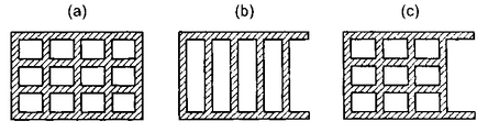
また、図6(a)に示されるように、連続した外枠を有する形状、図6(b)、(c)に示されるように、外枠の一部が切断されていることが好ましい。
電極層14の厚みは、0.1μm以上1000μm以下であることが好ましく、1μm以上500μm以下であることがより好ましく、5μm以上100μm以下であることがさらに好ましい。
電極層14の開口率は、熱電変換装置1の光透過性の観点から1%以上99%以下であることが好ましく、より好ましくは90%以上99%以下であり、さらに好ましくは95%以上99%以下である。開口率とは、熱電変換装置1の平面積に対する、電極層14が形成された領域を除いた領域の面積の割合である。
電極層14の線幅は、10nm~1000μmが好ましく、より好ましくは、10~500μmである。線幅が上記範囲であれば、導電性を損なうこと無く、良好な光透過性が得られる。開口率は以下のように求められる。
開口率(%)=[開口部の面積/(電極層の線部分の面積+開口部の面積)]×100
合金としては、金、銀、銅、白金から選ばれる少なくとも一種またはその一種を主体とする合金であれば特に限定されない。これらの合金としては、青銅、リン青銅、黄銅、白銅、モネル等が挙げられ、適宜選択可能である。とりわけ、銅を主体とする合金は導電性に優れ、加工性も良好なので、好ましく用いられる。
電極層14は、単層であってもよく、多層構造であってもよい。導電性を保持しながら耐腐食性を向上させることができるという点から、電極層は、多層構造であることが好ましい。
多層構造としては、同種の材料からなる層を積層した多層構造であってもよく、少なくとも2種類以上の材料からなる層を積層した多層構造であってもよい。
耐腐食性を向上させることができるという点から、少なくとも2種類以上の材料からなる層を積層した多層構造であることが好ましい。多層構造としては、基材11上に金、銀、銅、白金から選ばれる少なくとも一種、またはその一種を含む合金材料からなるパターン層を形成し、その上に、該パターン層を形成した材料よりも耐腐食性の高い材料からなるパターン層を積層することが好ましい。
多層構造としては、異種の材料からなる層を積層した2層構造であることがより好ましい。このような多層構造としては、例えば、最初に銀のパターン層を形成させ、その上から銀よりも耐腐食性の高い銅のパターン層を形成させると、銀の高導電性を保持しながら耐腐食性が改善される。
次に、熱電変換装置の作製方法について説明する。
基材11の表面に、上述した熱電材料を用いて電極層14が形成される。電極層14が形成された後、熱電変換層12及び13が形成される。さらに、再度、電極層14が形成される。
無機系材料を用いて熱電変換層を形成する方法としては、例えば、蒸着法、スパッタリング法、イオンプレーティング法、熱CVD法、プラズマCVD法等が挙げられる。これらの中でも、本発明においては、簡便に導電体層が形成できることから、スパッタリング法が好ましい。
スパッタリング法は、真空槽内に放電ガス(アルゴン等)を導入し、ターゲットと基板との間に高周波電圧あるいは直流電圧を加えて放電ガスをプラズマ化し、該プラズマをターゲットに衝突させることでターゲット材料を飛ばし、基材11に付着させて薄膜を得る方法である。ターゲットとしては、前記熱電変換層を形成する材料からなるものが使用される。
中でも、有機高分子化合物の水分散液または溶液(塗工液)を、ディップコーティング、スピンコーティング、スプレーコーティング、グラビアコーティング、ダイコーティング、ドクターブレード等の各種コーティング法により、基材11上に設けられた電極層14上に塗布することができる。
電極層を設けるための方法としては、真空蒸着、スパッタリング、イオンプレーティング等のPVD(物理気相蒸着)、もしくは熱CVD、原子層蒸着(ALD)等のCVD(化学気相蒸着)などのドライプロセス、またはディップコーティング、スピンコーティング、スプレーコーティング、グラビアコーティング、ダイコーティング、ドクターブレード等の各種コーティング法や電気化学的ディポジションなどのウェットプロセス、銀塩法等が挙げられ、導電性金属層の材料に応じて適宜選択される。
電極層14と基材11との密着性を向上させるために、光透過性を有する、従来公知のアクリル系樹脂、ポリウレタン系樹脂のようなプライマー層を介在させてもよい。
本発明の実施形態に係る蓄電システムの態様について説明する。蓄電システムは、熱電変換装置のほかに、電気を蓄電する蓄電装置を備える。熱電変換装置から得た電気エネルギーの蓄電動作を制御する制御回路を有していてもよい。
蓄電装置は二次電池やキャパシタ等で構成される。二次電池としては蓄電可能な電池あればよく、例えばリチウム電池、リチウムポリマー電池、リチウムイオン電池、ニッケル水素電池、ニカド電池、有機ラジカル電池、鉛蓄電池、空気二次電池、ニッケル亜鉛電池、銀亜鉛電池等が挙げられる。キャパシタとしては、例えば電気二重層キャパシタ、リチウムイオンキャパシタ等が挙げられる。
[評価方法]
後述する熱電変換装置の熱電性能を、以下の方法で評価した。
<電気伝導率及びゼーベック係数>
熱電変換層の電気伝導率及びゼーベック係数を熱電特性評価装置(アルバック理工株式会社製、「ZEM-3」)を用いて測定した。
<熱伝導率>
熱電変換層の熱伝導率を3ω法により測定した。
<出力電圧>
チラー(アズワン株式会社製、「LTCi-150H」と、水冷式クーラー(高木製作所株式会社製、「P-200S」)とを組み合わせた冷却装置と、ホットプレート(アズワン株式会社製、「THI-1000」)とを用いて温度勾配を形成した。すなわち、50℃に加熱したホットプレートを熱電変換装置の基材側に密着させるとともに、熱電変換装置の基材とは反対側に、0℃に設定したチラーを接触させて、熱電変換装置に温度勾配を付与した。この状態で、ホットプレートに接触する基材の温度と、チラーに接触する電極層上面の温度とを、Kタイプ熱電対とデータロガー(江藤電機株式会社製、「キャダック3」)とを組み合わせた測定装置で測定し、温度差を算出し、デジタルマルチメータ(日置電機株式会社製、「DT4282」)にて熱電変換装置の出力電圧を測定した。
<光透過率(%T550)>
分光光度計(島津製作所株式会社製、「UV3601」を用いて、JIS K7361-1に準拠して熱電変換装置の可視光透過率(550nmの透過率)を測定した。
熱電変換装置を、下記の通り作製した。
<実施例1>
ガラス基板(CORNING株式会社製、「イーグルXG」、厚み0.7mm)の表面上に、スクリーン印刷法を用いて銀ペーストをストライプ状に、かつ所定のパターンに印刷した後、150℃で30分乾燥し、所定パターンの光透過性電極層を形成した。
続いて、有機系p型熱電材料であるPEDOT:PSS(アグファマテリアル株式会社製、「S-305」、熱伝導率0.3W/m・K)を、インクジェット印刷装置(マイクロジェット株式会社製、「NanoPrinter-300」)を用いて、p型熱電変換層を形成した。形成後、大気中において150℃で乾燥した。続いて、スパッタリング法により、n型熱電材料であるガリウムドープ酸化亜鉛(GZO)を用いて、透明n型熱電変換層を形成した。
両方の熱電変換層を形成後、上記方法と同様にして、銀ペーストを所定のパターンに印刷した後、150℃で30分乾燥し、所定パターンの光透過性電極層を形成し、図1又は図2に示すタイプの熱電変換装置aを作製した。
熱電変換装置aにおける熱電変換層、及び電極層の寸法は、下記に示す通りである。すなわち、図1又は図2に示す各部位において、D11=8mm、D12=2mm、D13=2mm、d1=0.5mm、d2=0.5mm、とした。また、p型熱電変換層12の厚み(h12)及びn型熱電変換層の厚み(h13)は、0.2μm、電極層の厚み(h14)は0.1μmに設定した。
この供試体に、上述した方法により熱を与え、熱電変換装置aに生じる温度差を測定した。また、得られる電位差、及び熱電変換装置の光透過率を測定した。結果を、用いたp型熱電変換層及びn型熱電変換層のそれぞれの電気伝導率、熱伝導率とともに表1に示す。
ガラス基板(CORNING株式会社製、「イーグルXG」、厚み0.7mm)の表面上に、スクリーン印刷法を用いて銀ペーストを所定のパターンに印刷した後、150℃で30分乾燥し、所定パターンの光透過性電極を形成した。
続いて、有機系p型熱電材料であるPEDOT:PSS(アグファマテリアル株式会社製、「S-305」、熱伝導率0.3W/m・K)を、インクジェット印刷装置(マイクロジェット株式会社製、「NanoPrinter-300」)を用いて、p型熱電変換層を形成した。形成後、大気中において150℃で乾燥した。
続いて、上記方法と同様にして、銀ペーストを所定のパターンに印刷した後、150℃で30分乾燥し、所定パターンの光透過性電極を形成し、図3及び図4に示すタイプの熱電変換装置bを作製した。
熱電変換装置bにおける熱電変換層、及び電極層の寸法は、下記に示す通りである。すなわち、図3及び図4に示す各部位において、D21=8mm、D22=2mmとした。また、熱電変換層の厚み(h22)は、0.2μm、電極層の厚み(h23)は0.1μmに設定した。
この供試体に、上述した方法により熱を与え、熱電変換装置bに生じる温度差を測定した。また、得られる電位差、及び熱電変換装置の光透過率を測定した。結果を、用いたp型熱電変換層の電気伝導率、熱伝導率とともに表1に示す。
実施例1と同様にして、ガラス基板上に光透過性電極層を形成した後、スパッタリング法により、ガリウムドープ酸化亜鉛(GZO)を用いて、透明n型熱電変換層を形成した。熱電変換層の形成後、実施例1の方法と同様に所定パターンの光透過性電極層を形成し、図3及び図4に示すタイプの熱電変換装置cを作製した。熱電変換装置cにおける熱電変換層、及び電極層の寸法は、熱電変換装置bと同一とした。
この供試体に、上述した方法により熱を与え、熱電変換装置cに生じる温度差を測定した。また、得られる電位差、及び熱電変換装置の光透過率を測定した。結果を、用いたn型熱電変換層の電気伝導率、熱伝導率とともに表1に示す。
実施例1と同様にして、ガラス基板上にメッシュ構造を有する光透過性電極層を形成した後、スパッタリング法により、酸化インジウムスズ(ITO)を用いて、透明n型熱電変換層を形成した。熱電変換層の形成後、実施例1の方法と同様に所定パターンの光透過性電極層を形成し、図3及び図4に示すタイプの熱電変換装置dを作製した。熱電変換装置dにおける熱電変換層、及び電極層の寸法は、熱電変換装置bと同一とした。
この供試体に、上述した方法により熱を与え、熱電変換装置dに生じる温度差を測定した。また、得られる電位差、及び熱電変換装置の光透過率を測定した。結果を、用いたn型熱電変換層の電気伝導率、熱伝導率とともに表1に示す。

実施例1~4の供試体は、光透過性を備え、熱エネルギーから電気エネルギーを回生することが可能であることがわかった。
Claims (9)
- 熱電材料から形成された熱電変換層と、該熱電変換層に接続された電極層とを備える熱電変換装置であって、
該熱電変換層及び該電極層のうち少なくとも該熱電変換層が光透過性を有する熱電変換装置。 - 前記熱電変換層及び前記電極層のうち少なくとも前記熱電変換層が該熱電変換層の平面に交差する方向において、分光光度計を用いて測定される550nmの可視光透過率が60%以上である請求項1に記載の熱電変換装置。
- 前記熱電変換層と前記電極層とが表面に配設された基材を有し、該基材が光透過性を有する無機系材料又は光透過性を有する有機系材料である請求項1又は2に記載の熱電変換装置。
- 前記熱電材料がn型熱電材料である請求項1~3のいずれか1項に記載の熱電変換装置。
- 前記熱電材料がp型熱電材料である請求項1~3のいずれか1項に記載の熱電変換装置。
- 前記熱電変換層がn型熱電材料から形成されたn型熱電変換層及びp型熱電材料から形成されたp型熱電変換層を有し、該n型熱電変換層及び該p型熱電変換層が前記電極層によって接続されている請求項1~5のいずれか1項に記載の熱電変換装置。
- 前記熱電変換装置の平面積に対する、前記電極層が形成された領域を除く領域の面積の割合が1%以上99%以下である請求項1~6のいずれか1項に記載の熱電変換装置。
- 前記電極層が光透過性を有する請求項1~7のいずれか1項に記載の熱電変換装置。
- 請求項1~8のいずれかに記載の熱電変換装置と、電気を蓄電する蓄電装置とを備え、
該熱電変換装置における前記電極層が該蓄電装置に電気的に接続されてなる蓄電システム。
Priority Applications (3)
| Application Number | Priority Date | Filing Date | Title |
|---|---|---|---|
| KR1020177018289A KR20170102477A (ko) | 2015-01-08 | 2015-12-15 | 열전 변환 장치 및 축전 시스템 |
| JP2016568304A JPWO2016111125A1 (ja) | 2015-01-08 | 2015-12-15 | 熱電変換装置及び蓄電システム |
| CN201580072177.5A CN107112408A (zh) | 2015-01-08 | 2015-12-15 | 热电转换装置及蓄电系统 |
Applications Claiming Priority (2)
| Application Number | Priority Date | Filing Date | Title |
|---|---|---|---|
| JP2015002545 | 2015-01-08 | ||
| JP2015-002545 | 2015-01-08 |
Publications (1)
| Publication Number | Publication Date |
|---|---|
| WO2016111125A1 true WO2016111125A1 (ja) | 2016-07-14 |
Family
ID=56355827
Family Applications (1)
| Application Number | Title | Priority Date | Filing Date |
|---|---|---|---|
| PCT/JP2015/085110 Ceased WO2016111125A1 (ja) | 2015-01-08 | 2015-12-15 | 熱電変換装置及び蓄電システム |
Country Status (5)
| Country | Link |
|---|---|
| JP (1) | JPWO2016111125A1 (ja) |
| KR (1) | KR20170102477A (ja) |
| CN (1) | CN107112408A (ja) |
| TW (1) | TWI678818B (ja) |
| WO (1) | WO2016111125A1 (ja) |
Cited By (2)
| Publication number | Priority date | Publication date | Assignee | Title |
|---|---|---|---|---|
| JP2023530348A (ja) * | 2020-06-16 | 2023-07-14 | ビーワイディー カンパニー リミテッド | 半導体冷却チップ及びその製造方法 |
| JP2024016891A (ja) * | 2022-07-27 | 2024-02-08 | 国立研究開発法人物質・材料研究機構 | 発電装置、および、それを用いた発電システム |
Families Citing this family (1)
| Publication number | Priority date | Publication date | Assignee | Title |
|---|---|---|---|---|
| KR102612211B1 (ko) * | 2020-09-28 | 2023-12-11 | 경북대학교 산학협력단 | 산화 금속 입자를 포함한 유기 열전소자 |
Citations (6)
| Publication number | Priority date | Publication date | Assignee | Title |
|---|---|---|---|---|
| JPH07139750A (ja) * | 1993-11-15 | 1995-05-30 | Shimizu Corp | 窓面の顕熱負荷除去装置 |
| JP2005019783A (ja) * | 2003-06-27 | 2005-01-20 | Idemitsu Kosan Co Ltd | 熱電変換材料と電極の接合方法及び熱電変換モジュール |
| JP2009047969A (ja) * | 2007-08-21 | 2009-03-05 | Seiko Epson Corp | プロジェクタおよび表示装置 |
| JP2009055735A (ja) * | 2007-08-28 | 2009-03-12 | Toyota Motor Corp | 電気エネルギー回収装置 |
| JP2013102155A (ja) * | 2011-10-19 | 2013-05-23 | Fujifilm Corp | 熱電変換素子及びその製造方法 |
| WO2014034258A1 (ja) * | 2012-08-30 | 2014-03-06 | 独立行政法人産業技術総合研究所 | 熱電材料および熱電モジュール |
Family Cites Families (8)
| Publication number | Priority date | Publication date | Assignee | Title |
|---|---|---|---|---|
| JP4316896B2 (ja) * | 2003-01-09 | 2009-08-19 | 株式会社 日立ディスプレイズ | 表示装置とその製造方法 |
| JP2006080469A (ja) * | 2004-09-13 | 2006-03-23 | Mitsubishi Cable Ind Ltd | 窒化物半導体発光素子 |
| JP4579769B2 (ja) * | 2005-05-26 | 2010-11-10 | 篠田プラズマ株式会社 | アレイ型表示装置 |
| KR100913132B1 (ko) * | 2007-12-17 | 2009-08-19 | 한국전자통신연구원 | 전계 방출형 백라이트 유닛과 이에 이용되는 캐소드 구조물및 이의 제조 방법 |
| TWI419386B (zh) * | 2010-10-26 | 2013-12-11 | Ind Tech Res Inst | 可透光式熱電能量轉換裝置 |
| WO2012140800A1 (ja) * | 2011-04-11 | 2012-10-18 | Watanabe Takaya | 冷暖房装置 |
| JP2013219067A (ja) * | 2012-04-04 | 2013-10-24 | Canon Inc | 放射線検出装置の製造方法、放射線検出装置、及び放射線撮像システム |
| TW201409783A (zh) * | 2012-08-28 | 2014-03-01 | Juant Technology Co Ltd | 可透光的熱電致冷元件 |
-
2015
- 2015-12-15 KR KR1020177018289A patent/KR20170102477A/ko not_active Ceased
- 2015-12-15 JP JP2016568304A patent/JPWO2016111125A1/ja active Pending
- 2015-12-15 CN CN201580072177.5A patent/CN107112408A/zh active Pending
- 2015-12-15 WO PCT/JP2015/085110 patent/WO2016111125A1/ja not_active Ceased
- 2015-12-22 TW TW104143167A patent/TWI678818B/zh not_active IP Right Cessation
Patent Citations (6)
| Publication number | Priority date | Publication date | Assignee | Title |
|---|---|---|---|---|
| JPH07139750A (ja) * | 1993-11-15 | 1995-05-30 | Shimizu Corp | 窓面の顕熱負荷除去装置 |
| JP2005019783A (ja) * | 2003-06-27 | 2005-01-20 | Idemitsu Kosan Co Ltd | 熱電変換材料と電極の接合方法及び熱電変換モジュール |
| JP2009047969A (ja) * | 2007-08-21 | 2009-03-05 | Seiko Epson Corp | プロジェクタおよび表示装置 |
| JP2009055735A (ja) * | 2007-08-28 | 2009-03-12 | Toyota Motor Corp | 電気エネルギー回収装置 |
| JP2013102155A (ja) * | 2011-10-19 | 2013-05-23 | Fujifilm Corp | 熱電変換素子及びその製造方法 |
| WO2014034258A1 (ja) * | 2012-08-30 | 2014-03-06 | 独立行政法人産業技術総合研究所 | 熱電材料および熱電モジュール |
Cited By (3)
| Publication number | Priority date | Publication date | Assignee | Title |
|---|---|---|---|---|
| JP2023530348A (ja) * | 2020-06-16 | 2023-07-14 | ビーワイディー カンパニー リミテッド | 半導体冷却チップ及びその製造方法 |
| JP7680477B2 (ja) | 2020-06-16 | 2025-05-20 | ビーワイディー カンパニー リミテッド | 半導体冷却チップ及びその製造方法 |
| JP2024016891A (ja) * | 2022-07-27 | 2024-02-08 | 国立研究開発法人物質・材料研究機構 | 発電装置、および、それを用いた発電システム |
Also Published As
| Publication number | Publication date |
|---|---|
| CN107112408A (zh) | 2017-08-29 |
| TW201633573A (zh) | 2016-09-16 |
| JPWO2016111125A1 (ja) | 2017-10-12 |
| TWI678818B (zh) | 2019-12-01 |
| KR20170102477A (ko) | 2017-09-11 |
Similar Documents
| Publication | Publication Date | Title |
|---|---|---|
| EP2465006B1 (en) | Solid state lighting element comprising an electrode with improved optical and electrical performances | |
| KR101897278B1 (ko) | 투명 전극 기판, 그 제조 방법, 이 투명 전극 기판을 가지는 전자 디바이스 및 태양 전지 | |
| CN102779944B (zh) | 一种透明导电薄膜 | |
| Kim et al. | Highly flexible ZnO/Ag/ZnO conducting electrode for organic photonic devices | |
| TWI550463B (zh) | 導電膜及其製造方法 | |
| KR20140015290A (ko) | 투명 도전성 적층체 및 유기 박막 디바이스 | |
| JP5987843B2 (ja) | 透明電極形成用組成物、透明電極、有機電子素子および透明電極の製造方法 | |
| US20150279498A1 (en) | Transparent conductive thin film electrodes, electronic devices and methods of producing the same | |
| WO2011162080A1 (ja) | 有機エレクトロルミネッセンス素子 | |
| CN105144045A (zh) | 导电结构及其制造方法 | |
| US9640762B2 (en) | Method for producing transparent electrode and organic EL element | |
| JP2013222688A (ja) | 有機電子素子用透明電極、有機電子素子用透明電極の製造方法、及び有機電子素子 | |
| US11489081B2 (en) | Photoelectric conversion device and method of manufacturing photoelectric conversion device | |
| Kumar et al. | Transparent conductive Ta/Al/Ta-grid electrode for optoelectronic and electromagnetic interference shielding applications | |
| WO2016111125A1 (ja) | 熱電変換装置及び蓄電システム | |
| KR101273798B1 (ko) | 다층 투명전극 및 그 제조방법 | |
| JP2014229397A (ja) | 導電膜の製造方法、導電膜、有機電子素子及びタッチパネル | |
| Wang et al. | An efficient flexible white organic light-emitting device with a screen-printed conducting polymer anode | |
| He et al. | Patterned few nanometer-thick silver films with high optical transparency and high electrical conductivity | |
| JP2014104409A (ja) | 透明電極の製造方法 | |
| KR20150105798A (ko) | 투명전극 및 그 제조방법 | |
| KR20140090876A (ko) | 다층 구조의 투명 전극 | |
| Kim et al. | ZnSnO/Ag/indium tin oxide multilayer films as a flexible and transparent electrode for photonic devices | |
| Kim et al. | Fully vacuum-free fabrication of bi-directional polymer light-emitting diodes based on a hybrid lamination top electrode | |
| JP2016110769A (ja) | 透明電極の製造方法、透明電極、透明電極の製造装置、電子機器 |
Legal Events
| Date | Code | Title | Description |
|---|---|---|---|
| 121 | Ep: the epo has been informed by wipo that ep was designated in this application |
Ref document number: 15876998 Country of ref document: EP Kind code of ref document: A1 |
|
| ENP | Entry into the national phase |
Ref document number: 2016568304 Country of ref document: JP Kind code of ref document: A |
|
| ENP | Entry into the national phase |
Ref document number: 20177018289 Country of ref document: KR Kind code of ref document: A |
|
| NENP | Non-entry into the national phase |
Ref country code: DE |
|
| 122 | Ep: pct application non-entry in european phase |
Ref document number: 15876998 Country of ref document: EP Kind code of ref document: A1 |