WO2016103114A1 - スパッタリング用ターゲットの作製方法 - Google Patents
スパッタリング用ターゲットの作製方法 Download PDFInfo
- Publication number
- WO2016103114A1 WO2016103114A1 PCT/IB2015/059650 IB2015059650W WO2016103114A1 WO 2016103114 A1 WO2016103114 A1 WO 2016103114A1 IB 2015059650 W IB2015059650 W IB 2015059650W WO 2016103114 A1 WO2016103114 A1 WO 2016103114A1
- Authority
- WO
- WIPO (PCT)
- Prior art keywords
- semiconductor
- substrate
- oxide
- conductor
- target
- Prior art date
- Legal status (The legal status is an assumption and is not a legal conclusion. Google has not performed a legal analysis and makes no representation as to the accuracy of the status listed.)
- Ceased
Links
- XDTMQSROBMDMFD-UHFFFAOYSA-N C1CCCCC1 Chemical compound C1CCCCC1 XDTMQSROBMDMFD-UHFFFAOYSA-N 0.000 description 1
- AVFZOVWCLRSYKC-UHFFFAOYSA-N CN1CCCC1 Chemical compound CN1CCCC1 AVFZOVWCLRSYKC-UHFFFAOYSA-N 0.000 description 1
Images



























Classifications
-
- C—CHEMISTRY; METALLURGY
- C23—COATING METALLIC MATERIAL; COATING MATERIAL WITH METALLIC MATERIAL; CHEMICAL SURFACE TREATMENT; DIFFUSION TREATMENT OF METALLIC MATERIAL; COATING BY VACUUM EVAPORATION, BY SPUTTERING, BY ION IMPLANTATION OR BY CHEMICAL VAPOUR DEPOSITION, IN GENERAL; INHIBITING CORROSION OF METALLIC MATERIAL OR INCRUSTATION IN GENERAL
- C23C—COATING METALLIC MATERIAL; COATING MATERIAL WITH METALLIC MATERIAL; SURFACE TREATMENT OF METALLIC MATERIAL BY DIFFUSION INTO THE SURFACE, BY CHEMICAL CONVERSION OR SUBSTITUTION; COATING BY VACUUM EVAPORATION, BY SPUTTERING, BY ION IMPLANTATION OR BY CHEMICAL VAPOUR DEPOSITION, IN GENERAL
- C23C14/00—Coating by vacuum evaporation, by sputtering or by ion implantation of the coating forming material
- C23C14/22—Coating by vacuum evaporation, by sputtering or by ion implantation of the coating forming material characterised by the process of coating
- C23C14/34—Sputtering
- C23C14/3407—Cathode assembly for sputtering apparatus, e.g. Target
- C23C14/3414—Metallurgical or chemical aspects of target preparation, e.g. casting, powder metallurgy
-
- C—CHEMISTRY; METALLURGY
- C01—INORGANIC CHEMISTRY
- C01G—COMPOUNDS CONTAINING METALS NOT COVERED BY SUBCLASSES C01D OR C01F
- C01G15/00—Compounds of gallium, indium or thallium
- C01G15/006—Compounds containing gallium, indium or thallium, with or without oxygen or hydrogen, and containing two or more other elements
-
- C—CHEMISTRY; METALLURGY
- C01—INORGANIC CHEMISTRY
- C01G—COMPOUNDS CONTAINING METALS NOT COVERED BY SUBCLASSES C01D OR C01F
- C01G19/00—Compounds of tin
- C01G19/006—Compounds containing tin, with or without oxygen or hydrogen, and containing two or more other elements
-
- C—CHEMISTRY; METALLURGY
- C01—INORGANIC CHEMISTRY
- C01G—COMPOUNDS CONTAINING METALS NOT COVERED BY SUBCLASSES C01D OR C01F
- C01G19/00—Compounds of tin
- C01G19/02—Oxides
-
- C—CHEMISTRY; METALLURGY
- C01—INORGANIC CHEMISTRY
- C01G—COMPOUNDS CONTAINING METALS NOT COVERED BY SUBCLASSES C01D OR C01F
- C01G9/00—Compounds of zinc
- C01G9/006—Compounds containing zinc, with or without oxygen or hydrogen, and containing two or more other elements
-
- C—CHEMISTRY; METALLURGY
- C01—INORGANIC CHEMISTRY
- C01G—COMPOUNDS CONTAINING METALS NOT COVERED BY SUBCLASSES C01D OR C01F
- C01G9/00—Compounds of zinc
- C01G9/02—Oxides; Hydroxides
-
- C—CHEMISTRY; METALLURGY
- C04—CEMENTS; CONCRETE; ARTIFICIAL STONE; CERAMICS; REFRACTORIES
- C04B—LIME, MAGNESIA; SLAG; CEMENTS; COMPOSITIONS THEREOF, e.g. MORTARS, CONCRETE OR LIKE BUILDING MATERIALS; ARTIFICIAL STONE; CERAMICS; REFRACTORIES; TREATMENT OF NATURAL STONE
- C04B35/00—Shaped ceramic products characterised by their composition; Ceramics compositions; Processing powders of inorganic compounds preparatory to the manufacturing of ceramic products
- C04B35/01—Shaped ceramic products characterised by their composition; Ceramics compositions; Processing powders of inorganic compounds preparatory to the manufacturing of ceramic products based on oxide ceramics
-
- C—CHEMISTRY; METALLURGY
- C04—CEMENTS; CONCRETE; ARTIFICIAL STONE; CERAMICS; REFRACTORIES
- C04B—LIME, MAGNESIA; SLAG; CEMENTS; COMPOSITIONS THEREOF, e.g. MORTARS, CONCRETE OR LIKE BUILDING MATERIALS; ARTIFICIAL STONE; CERAMICS; REFRACTORIES; TREATMENT OF NATURAL STONE
- C04B35/00—Shaped ceramic products characterised by their composition; Ceramics compositions; Processing powders of inorganic compounds preparatory to the manufacturing of ceramic products
- C04B35/01—Shaped ceramic products characterised by their composition; Ceramics compositions; Processing powders of inorganic compounds preparatory to the manufacturing of ceramic products based on oxide ceramics
- C04B35/10—Shaped ceramic products characterised by their composition; Ceramics compositions; Processing powders of inorganic compounds preparatory to the manufacturing of ceramic products based on oxide ceramics based on aluminium oxide
- C04B35/111—Fine ceramics
- C04B35/117—Composites
-
- C—CHEMISTRY; METALLURGY
- C04—CEMENTS; CONCRETE; ARTIFICIAL STONE; CERAMICS; REFRACTORIES
- C04B—LIME, MAGNESIA; SLAG; CEMENTS; COMPOSITIONS THEREOF, e.g. MORTARS, CONCRETE OR LIKE BUILDING MATERIALS; ARTIFICIAL STONE; CERAMICS; REFRACTORIES; TREATMENT OF NATURAL STONE
- C04B35/00—Shaped ceramic products characterised by their composition; Ceramics compositions; Processing powders of inorganic compounds preparatory to the manufacturing of ceramic products
- C04B35/01—Shaped ceramic products characterised by their composition; Ceramics compositions; Processing powders of inorganic compounds preparatory to the manufacturing of ceramic products based on oxide ceramics
- C04B35/44—Shaped ceramic products characterised by their composition; Ceramics compositions; Processing powders of inorganic compounds preparatory to the manufacturing of ceramic products based on oxide ceramics based on aluminates
-
- C—CHEMISTRY; METALLURGY
- C04—CEMENTS; CONCRETE; ARTIFICIAL STONE; CERAMICS; REFRACTORIES
- C04B—LIME, MAGNESIA; SLAG; CEMENTS; COMPOSITIONS THEREOF, e.g. MORTARS, CONCRETE OR LIKE BUILDING MATERIALS; ARTIFICIAL STONE; CERAMICS; REFRACTORIES; TREATMENT OF NATURAL STONE
- C04B35/00—Shaped ceramic products characterised by their composition; Ceramics compositions; Processing powders of inorganic compounds preparatory to the manufacturing of ceramic products
- C04B35/01—Shaped ceramic products characterised by their composition; Ceramics compositions; Processing powders of inorganic compounds preparatory to the manufacturing of ceramic products based on oxide ceramics
- C04B35/453—Shaped ceramic products characterised by their composition; Ceramics compositions; Processing powders of inorganic compounds preparatory to the manufacturing of ceramic products based on oxide ceramics based on zinc, tin, or bismuth oxides or solid solutions thereof with other oxides, e.g. zincates, stannates or bismuthates
-
- C—CHEMISTRY; METALLURGY
- C04—CEMENTS; CONCRETE; ARTIFICIAL STONE; CERAMICS; REFRACTORIES
- C04B—LIME, MAGNESIA; SLAG; CEMENTS; COMPOSITIONS THEREOF, e.g. MORTARS, CONCRETE OR LIKE BUILDING MATERIALS; ARTIFICIAL STONE; CERAMICS; REFRACTORIES; TREATMENT OF NATURAL STONE
- C04B35/00—Shaped ceramic products characterised by their composition; Ceramics compositions; Processing powders of inorganic compounds preparatory to the manufacturing of ceramic products
- C04B35/01—Shaped ceramic products characterised by their composition; Ceramics compositions; Processing powders of inorganic compounds preparatory to the manufacturing of ceramic products based on oxide ceramics
- C04B35/453—Shaped ceramic products characterised by their composition; Ceramics compositions; Processing powders of inorganic compounds preparatory to the manufacturing of ceramic products based on oxide ceramics based on zinc, tin, or bismuth oxides or solid solutions thereof with other oxides, e.g. zincates, stannates or bismuthates
- C04B35/457—Shaped ceramic products characterised by their composition; Ceramics compositions; Processing powders of inorganic compounds preparatory to the manufacturing of ceramic products based on oxide ceramics based on zinc, tin, or bismuth oxides or solid solutions thereof with other oxides, e.g. zincates, stannates or bismuthates based on tin oxides or stannates
-
- C—CHEMISTRY; METALLURGY
- C04—CEMENTS; CONCRETE; ARTIFICIAL STONE; CERAMICS; REFRACTORIES
- C04B—LIME, MAGNESIA; SLAG; CEMENTS; COMPOSITIONS THEREOF, e.g. MORTARS, CONCRETE OR LIKE BUILDING MATERIALS; ARTIFICIAL STONE; CERAMICS; REFRACTORIES; TREATMENT OF NATURAL STONE
- C04B35/00—Shaped ceramic products characterised by their composition; Ceramics compositions; Processing powders of inorganic compounds preparatory to the manufacturing of ceramic products
- C04B35/50—Shaped ceramic products characterised by their composition; Ceramics compositions; Processing powders of inorganic compounds preparatory to the manufacturing of ceramic products based on rare-earth compounds
- C04B35/505—Shaped ceramic products characterised by their composition; Ceramics compositions; Processing powders of inorganic compounds preparatory to the manufacturing of ceramic products based on rare-earth compounds based on yttrium oxide
-
- C—CHEMISTRY; METALLURGY
- C04—CEMENTS; CONCRETE; ARTIFICIAL STONE; CERAMICS; REFRACTORIES
- C04B—LIME, MAGNESIA; SLAG; CEMENTS; COMPOSITIONS THEREOF, e.g. MORTARS, CONCRETE OR LIKE BUILDING MATERIALS; ARTIFICIAL STONE; CERAMICS; REFRACTORIES; TREATMENT OF NATURAL STONE
- C04B35/00—Shaped ceramic products characterised by their composition; Ceramics compositions; Processing powders of inorganic compounds preparatory to the manufacturing of ceramic products
- C04B35/622—Forming processes; Processing powders of inorganic compounds preparatory to the manufacturing of ceramic products
- C04B35/64—Burning or sintering processes
-
- C—CHEMISTRY; METALLURGY
- C23—COATING METALLIC MATERIAL; COATING MATERIAL WITH METALLIC MATERIAL; CHEMICAL SURFACE TREATMENT; DIFFUSION TREATMENT OF METALLIC MATERIAL; COATING BY VACUUM EVAPORATION, BY SPUTTERING, BY ION IMPLANTATION OR BY CHEMICAL VAPOUR DEPOSITION, IN GENERAL; INHIBITING CORROSION OF METALLIC MATERIAL OR INCRUSTATION IN GENERAL
- C23C—COATING METALLIC MATERIAL; COATING MATERIAL WITH METALLIC MATERIAL; SURFACE TREATMENT OF METALLIC MATERIAL BY DIFFUSION INTO THE SURFACE, BY CHEMICAL CONVERSION OR SUBSTITUTION; COATING BY VACUUM EVAPORATION, BY SPUTTERING, BY ION IMPLANTATION OR BY CHEMICAL VAPOUR DEPOSITION, IN GENERAL
- C23C14/00—Coating by vacuum evaporation, by sputtering or by ion implantation of the coating forming material
- C23C14/06—Coating by vacuum evaporation, by sputtering or by ion implantation of the coating forming material characterised by the coating material
- C23C14/08—Oxides
- C23C14/086—Oxides of zinc, germanium, cadmium, indium, tin, thallium or bismuth
-
- C—CHEMISTRY; METALLURGY
- C23—COATING METALLIC MATERIAL; COATING MATERIAL WITH METALLIC MATERIAL; CHEMICAL SURFACE TREATMENT; DIFFUSION TREATMENT OF METALLIC MATERIAL; COATING BY VACUUM EVAPORATION, BY SPUTTERING, BY ION IMPLANTATION OR BY CHEMICAL VAPOUR DEPOSITION, IN GENERAL; INHIBITING CORROSION OF METALLIC MATERIAL OR INCRUSTATION IN GENERAL
- C23C—COATING METALLIC MATERIAL; COATING MATERIAL WITH METALLIC MATERIAL; SURFACE TREATMENT OF METALLIC MATERIAL BY DIFFUSION INTO THE SURFACE, BY CHEMICAL CONVERSION OR SUBSTITUTION; COATING BY VACUUM EVAPORATION, BY SPUTTERING, BY ION IMPLANTATION OR BY CHEMICAL VAPOUR DEPOSITION, IN GENERAL
- C23C14/00—Coating by vacuum evaporation, by sputtering or by ion implantation of the coating forming material
- C23C14/22—Coating by vacuum evaporation, by sputtering or by ion implantation of the coating forming material characterised by the process of coating
- C23C14/34—Sputtering
-
- C—CHEMISTRY; METALLURGY
- C30—CRYSTAL GROWTH
- C30B—SINGLE-CRYSTAL GROWTH; UNIDIRECTIONAL SOLIDIFICATION OF EUTECTIC MATERIAL OR UNIDIRECTIONAL DEMIXING OF EUTECTOID MATERIAL; REFINING BY ZONE-MELTING OF MATERIAL; PRODUCTION OF A HOMOGENEOUS POLYCRYSTALLINE MATERIAL WITH DEFINED STRUCTURE; SINGLE CRYSTALS OR HOMOGENEOUS POLYCRYSTALLINE MATERIAL WITH DEFINED STRUCTURE; AFTER-TREATMENT OF SINGLE CRYSTALS OR A HOMOGENEOUS POLYCRYSTALLINE MATERIAL WITH DEFINED STRUCTURE; APPARATUS THEREFOR
- C30B23/00—Single-crystal growth by condensing evaporated or sublimed materials
- C30B23/02—Epitaxial-layer growth
-
- C—CHEMISTRY; METALLURGY
- C30—CRYSTAL GROWTH
- C30B—SINGLE-CRYSTAL GROWTH; UNIDIRECTIONAL SOLIDIFICATION OF EUTECTIC MATERIAL OR UNIDIRECTIONAL DEMIXING OF EUTECTOID MATERIAL; REFINING BY ZONE-MELTING OF MATERIAL; PRODUCTION OF A HOMOGENEOUS POLYCRYSTALLINE MATERIAL WITH DEFINED STRUCTURE; SINGLE CRYSTALS OR HOMOGENEOUS POLYCRYSTALLINE MATERIAL WITH DEFINED STRUCTURE; AFTER-TREATMENT OF SINGLE CRYSTALS OR A HOMOGENEOUS POLYCRYSTALLINE MATERIAL WITH DEFINED STRUCTURE; APPARATUS THEREFOR
- C30B29/00—Single crystals or homogeneous polycrystalline material with defined structure characterised by the material or by their shape
- C30B29/10—Inorganic compounds or compositions
- C30B29/16—Oxides
- C30B29/22—Complex oxides
-
- H—ELECTRICITY
- H01—ELECTRIC ELEMENTS
- H01J—ELECTRIC DISCHARGE TUBES OR DISCHARGE LAMPS
- H01J37/00—Discharge tubes with provision for introducing objects or material to be exposed to the discharge, e.g. for the purpose of examination or processing thereof
- H01J37/32—Gas-filled discharge tubes
- H01J37/34—Gas-filled discharge tubes operating with cathodic sputtering
- H01J37/3411—Constructional aspects of the reactor
- H01J37/3414—Targets
- H01J37/3426—Material
-
- H—ELECTRICITY
- H10—SEMICONDUCTOR DEVICES; ELECTRIC SOLID-STATE DEVICES NOT OTHERWISE PROVIDED FOR
- H10D—INORGANIC ELECTRIC SEMICONDUCTOR DEVICES
- H10D30/00—Field-effect transistors [FET]
- H10D30/60—Insulated-gate field-effect transistors [IGFET]
- H10D30/67—Thin-film transistors [TFT]
-
- H—ELECTRICITY
- H10—SEMICONDUCTOR DEVICES; ELECTRIC SOLID-STATE DEVICES NOT OTHERWISE PROVIDED FOR
- H10D—INORGANIC ELECTRIC SEMICONDUCTOR DEVICES
- H10D30/00—Field-effect transistors [FET]
- H10D30/60—Insulated-gate field-effect transistors [IGFET]
- H10D30/67—Thin-film transistors [TFT]
- H10D30/674—Thin-film transistors [TFT] characterised by the active materials
- H10D30/6755—Oxide semiconductors, e.g. zinc oxide, copper aluminium oxide or cadmium stannate
-
- H—ELECTRICITY
- H10—SEMICONDUCTOR DEVICES; ELECTRIC SOLID-STATE DEVICES NOT OTHERWISE PROVIDED FOR
- H10D—INORGANIC ELECTRIC SEMICONDUCTOR DEVICES
- H10D86/00—Integrated devices formed in or on insulating or conducting substrates, e.g. formed in silicon-on-insulator [SOI] substrates or on stainless steel or glass substrates
- H10D86/40—Integrated devices formed in or on insulating or conducting substrates, e.g. formed in silicon-on-insulator [SOI] substrates or on stainless steel or glass substrates characterised by multiple TFTs
- H10D86/421—Integrated devices formed in or on insulating or conducting substrates, e.g. formed in silicon-on-insulator [SOI] substrates or on stainless steel or glass substrates characterised by multiple TFTs having a particular composition, shape or crystalline structure of the active layer
- H10D86/423—Integrated devices formed in or on insulating or conducting substrates, e.g. formed in silicon-on-insulator [SOI] substrates or on stainless steel or glass substrates characterised by multiple TFTs having a particular composition, shape or crystalline structure of the active layer comprising semiconductor materials not belonging to the Group IV, e.g. InGaZnO
-
- H—ELECTRICITY
- H10—SEMICONDUCTOR DEVICES; ELECTRIC SOLID-STATE DEVICES NOT OTHERWISE PROVIDED FOR
- H10D—INORGANIC ELECTRIC SEMICONDUCTOR DEVICES
- H10D86/00—Integrated devices formed in or on insulating or conducting substrates, e.g. formed in silicon-on-insulator [SOI] substrates or on stainless steel or glass substrates
- H10D86/40—Integrated devices formed in or on insulating or conducting substrates, e.g. formed in silicon-on-insulator [SOI] substrates or on stainless steel or glass substrates characterised by multiple TFTs
- H10D86/60—Integrated devices formed in or on insulating or conducting substrates, e.g. formed in silicon-on-insulator [SOI] substrates or on stainless steel or glass substrates characterised by multiple TFTs wherein the TFTs are in active matrices
-
- H—ELECTRICITY
- H10—SEMICONDUCTOR DEVICES; ELECTRIC SOLID-STATE DEVICES NOT OTHERWISE PROVIDED FOR
- H10D—INORGANIC ELECTRIC SEMICONDUCTOR DEVICES
- H10D87/00—Integrated devices comprising both bulk components and either SOI or SOS components on the same substrate
-
- C—CHEMISTRY; METALLURGY
- C01—INORGANIC CHEMISTRY
- C01P—INDEXING SCHEME RELATING TO STRUCTURAL AND PHYSICAL ASPECTS OF SOLID INORGANIC COMPOUNDS
- C01P2006/00—Physical properties of inorganic compounds
- C01P2006/80—Compositional purity
-
- C—CHEMISTRY; METALLURGY
- C04—CEMENTS; CONCRETE; ARTIFICIAL STONE; CERAMICS; REFRACTORIES
- C04B—LIME, MAGNESIA; SLAG; CEMENTS; COMPOSITIONS THEREOF, e.g. MORTARS, CONCRETE OR LIKE BUILDING MATERIALS; ARTIFICIAL STONE; CERAMICS; REFRACTORIES; TREATMENT OF NATURAL STONE
- C04B2235/00—Aspects relating to ceramic starting mixtures or sintered ceramic products
- C04B2235/02—Composition of constituents of the starting material or of secondary phases of the final product
- C04B2235/30—Constituents and secondary phases not being of a fibrous nature
- C04B2235/32—Metal oxides, mixed metal oxides, or oxide-forming salts thereof, e.g. carbonates, nitrates, (oxy)hydroxides, chlorides
- C04B2235/3217—Aluminum oxide or oxide forming salts thereof, e.g. bauxite, alpha-alumina
-
- C—CHEMISTRY; METALLURGY
- C04—CEMENTS; CONCRETE; ARTIFICIAL STONE; CERAMICS; REFRACTORIES
- C04B—LIME, MAGNESIA; SLAG; CEMENTS; COMPOSITIONS THEREOF, e.g. MORTARS, CONCRETE OR LIKE BUILDING MATERIALS; ARTIFICIAL STONE; CERAMICS; REFRACTORIES; TREATMENT OF NATURAL STONE
- C04B2235/00—Aspects relating to ceramic starting mixtures or sintered ceramic products
- C04B2235/02—Composition of constituents of the starting material or of secondary phases of the final product
- C04B2235/30—Constituents and secondary phases not being of a fibrous nature
- C04B2235/32—Metal oxides, mixed metal oxides, or oxide-forming salts thereof, e.g. carbonates, nitrates, (oxy)hydroxides, chlorides
- C04B2235/3224—Rare earth oxide or oxide forming salts thereof, e.g. scandium oxide
- C04B2235/3225—Yttrium oxide or oxide-forming salts thereof
-
- C—CHEMISTRY; METALLURGY
- C04—CEMENTS; CONCRETE; ARTIFICIAL STONE; CERAMICS; REFRACTORIES
- C04B—LIME, MAGNESIA; SLAG; CEMENTS; COMPOSITIONS THEREOF, e.g. MORTARS, CONCRETE OR LIKE BUILDING MATERIALS; ARTIFICIAL STONE; CERAMICS; REFRACTORIES; TREATMENT OF NATURAL STONE
- C04B2235/00—Aspects relating to ceramic starting mixtures or sintered ceramic products
- C04B2235/02—Composition of constituents of the starting material or of secondary phases of the final product
- C04B2235/30—Constituents and secondary phases not being of a fibrous nature
- C04B2235/32—Metal oxides, mixed metal oxides, or oxide-forming salts thereof, e.g. carbonates, nitrates, (oxy)hydroxides, chlorides
- C04B2235/3286—Gallium oxides, gallates, indium oxides, indates, thallium oxides, thallates or oxide forming salts thereof, e.g. zinc gallate
-
- C—CHEMISTRY; METALLURGY
- C04—CEMENTS; CONCRETE; ARTIFICIAL STONE; CERAMICS; REFRACTORIES
- C04B—LIME, MAGNESIA; SLAG; CEMENTS; COMPOSITIONS THEREOF, e.g. MORTARS, CONCRETE OR LIKE BUILDING MATERIALS; ARTIFICIAL STONE; CERAMICS; REFRACTORIES; TREATMENT OF NATURAL STONE
- C04B2235/00—Aspects relating to ceramic starting mixtures or sintered ceramic products
- C04B2235/02—Composition of constituents of the starting material or of secondary phases of the final product
- C04B2235/30—Constituents and secondary phases not being of a fibrous nature
- C04B2235/32—Metal oxides, mixed metal oxides, or oxide-forming salts thereof, e.g. carbonates, nitrates, (oxy)hydroxides, chlorides
- C04B2235/3293—Tin oxides, stannates or oxide forming salts thereof, e.g. indium tin oxide [ITO]
-
- C—CHEMISTRY; METALLURGY
- C04—CEMENTS; CONCRETE; ARTIFICIAL STONE; CERAMICS; REFRACTORIES
- C04B—LIME, MAGNESIA; SLAG; CEMENTS; COMPOSITIONS THEREOF, e.g. MORTARS, CONCRETE OR LIKE BUILDING MATERIALS; ARTIFICIAL STONE; CERAMICS; REFRACTORIES; TREATMENT OF NATURAL STONE
- C04B2235/00—Aspects relating to ceramic starting mixtures or sintered ceramic products
- C04B2235/65—Aspects relating to heat treatments of ceramic bodies such as green ceramics or pre-sintered ceramics, e.g. burning, sintering or melting processes
- C04B2235/656—Aspects relating to heat treatments of ceramic bodies such as green ceramics or pre-sintered ceramics, e.g. burning, sintering or melting processes characterised by specific heating conditions during heat treatment
-
- C—CHEMISTRY; METALLURGY
- C04—CEMENTS; CONCRETE; ARTIFICIAL STONE; CERAMICS; REFRACTORIES
- C04B—LIME, MAGNESIA; SLAG; CEMENTS; COMPOSITIONS THEREOF, e.g. MORTARS, CONCRETE OR LIKE BUILDING MATERIALS; ARTIFICIAL STONE; CERAMICS; REFRACTORIES; TREATMENT OF NATURAL STONE
- C04B2235/00—Aspects relating to ceramic starting mixtures or sintered ceramic products
- C04B2235/65—Aspects relating to heat treatments of ceramic bodies such as green ceramics or pre-sintered ceramics, e.g. burning, sintering or melting processes
- C04B2235/658—Atmosphere during thermal treatment
-
- C—CHEMISTRY; METALLURGY
- C04—CEMENTS; CONCRETE; ARTIFICIAL STONE; CERAMICS; REFRACTORIES
- C04B—LIME, MAGNESIA; SLAG; CEMENTS; COMPOSITIONS THEREOF, e.g. MORTARS, CONCRETE OR LIKE BUILDING MATERIALS; ARTIFICIAL STONE; CERAMICS; REFRACTORIES; TREATMENT OF NATURAL STONE
- C04B2235/00—Aspects relating to ceramic starting mixtures or sintered ceramic products
- C04B2235/65—Aspects relating to heat treatments of ceramic bodies such as green ceramics or pre-sintered ceramics, e.g. burning, sintering or melting processes
- C04B2235/658—Atmosphere during thermal treatment
- C04B2235/6583—Oxygen containing atmosphere, e.g. with changing oxygen pressures
-
- C—CHEMISTRY; METALLURGY
- C04—CEMENTS; CONCRETE; ARTIFICIAL STONE; CERAMICS; REFRACTORIES
- C04B—LIME, MAGNESIA; SLAG; CEMENTS; COMPOSITIONS THEREOF, e.g. MORTARS, CONCRETE OR LIKE BUILDING MATERIALS; ARTIFICIAL STONE; CERAMICS; REFRACTORIES; TREATMENT OF NATURAL STONE
- C04B2235/00—Aspects relating to ceramic starting mixtures or sintered ceramic products
- C04B2235/65—Aspects relating to heat treatments of ceramic bodies such as green ceramics or pre-sintered ceramics, e.g. burning, sintering or melting processes
- C04B2235/66—Specific sintering techniques, e.g. centrifugal sintering
- C04B2235/661—Multi-step sintering
-
- C—CHEMISTRY; METALLURGY
- C04—CEMENTS; CONCRETE; ARTIFICIAL STONE; CERAMICS; REFRACTORIES
- C04B—LIME, MAGNESIA; SLAG; CEMENTS; COMPOSITIONS THEREOF, e.g. MORTARS, CONCRETE OR LIKE BUILDING MATERIALS; ARTIFICIAL STONE; CERAMICS; REFRACTORIES; TREATMENT OF NATURAL STONE
- C04B2235/00—Aspects relating to ceramic starting mixtures or sintered ceramic products
- C04B2235/65—Aspects relating to heat treatments of ceramic bodies such as green ceramics or pre-sintered ceramics, e.g. burning, sintering or melting processes
- C04B2235/66—Specific sintering techniques, e.g. centrifugal sintering
- C04B2235/661—Multi-step sintering
- C04B2235/662—Annealing after sintering
-
- H—ELECTRICITY
- H10—SEMICONDUCTOR DEVICES; ELECTRIC SOLID-STATE DEVICES NOT OTHERWISE PROVIDED FOR
- H10D—INORGANIC ELECTRIC SEMICONDUCTOR DEVICES
- H10D30/00—Field-effect transistors [FET]
- H10D30/40—FETs having zero-dimensional [0D], one-dimensional [1D] or two-dimensional [2D] charge carrier gas channels
- H10D30/47—FETs having zero-dimensional [0D], one-dimensional [1D] or two-dimensional [2D] charge carrier gas channels having two-dimensional [2D] charge carrier gas channels, e.g. nanoribbon FETs or high electron mobility transistors [HEMT]
- H10D30/471—High electron mobility transistors [HEMT] or high hole mobility transistors [HHMT]
- H10D30/473—High electron mobility transistors [HEMT] or high hole mobility transistors [HHMT] having confinement of carriers by multiple heterojunctions, e.g. quantum well HEMT
-
- H—ELECTRICITY
- H10—SEMICONDUCTOR DEVICES; ELECTRIC SOLID-STATE DEVICES NOT OTHERWISE PROVIDED FOR
- H10D—INORGANIC ELECTRIC SEMICONDUCTOR DEVICES
- H10D62/00—Semiconductor bodies, or regions thereof, of devices having potential barriers
- H10D62/80—Semiconductor bodies, or regions thereof, of devices having potential barriers characterised by the materials
-
- H—ELECTRICITY
- H10—SEMICONDUCTOR DEVICES; ELECTRIC SOLID-STATE DEVICES NOT OTHERWISE PROVIDED FOR
- H10D—INORGANIC ELECTRIC SEMICONDUCTOR DEVICES
- H10D62/00—Semiconductor bodies, or regions thereof, of devices having potential barriers
- H10D62/80—Semiconductor bodies, or regions thereof, of devices having potential barriers characterised by the materials
- H10D62/875—Semiconductor bodies, or regions thereof, of devices having potential barriers characterised by the materials being semiconductor metal oxide, e.g. InGaZnO
Definitions
- the present invention relates to a sputtering target and a manufacturing method thereof.
- the present invention relates to an oxide, a transistor, a semiconductor device, and a manufacturing method thereof, for example.
- the present invention relates to an oxide, a display device, a light-emitting device, a lighting device, a power storage device, a memory device, a processor, and an electronic device, for example.
- the present invention relates to a method for manufacturing an oxide, a display device, a liquid crystal display device, a light-emitting device, a memory device, and an electronic device.
- the present invention relates to a driving method of a semiconductor device, a display device, a liquid crystal display device, a light-emitting device, a memory device, or an electronic device.
- one embodiment of the present invention is not limited to the above technical field.
- the technical field of one embodiment of the invention disclosed in this specification and the like relates to an object, a method, or a manufacturing method.
- one embodiment of the present invention relates to a process, a machine, a manufacture, or a composition (composition of matter).
- a semiconductor device refers to any device that can function by utilizing semiconductor characteristics.
- a display device, a light-emitting device, a lighting device, an electro-optical device, a semiconductor circuit, and an electronic device may include a semiconductor device.
- a technique for forming a transistor using a semiconductor over a substrate having an insulating surface has attracted attention.
- the transistor is widely applied to semiconductor devices such as integrated circuits and display devices.
- Silicon is known as a semiconductor applicable to a transistor.
- amorphous silicon and polycrystalline silicon are selectively used depending on applications.
- silicon used for a transistor included in a large display device
- silicon when silicon is applied to a transistor that constitutes a high-performance display device in which a driver circuit and a pixel circuit are formed over the same substrate, polycrystalline silicon capable of manufacturing a transistor having high field effect mobility is used. It is preferable.
- a method of forming polycrystalline silicon by performing heat treatment at high temperature or laser light treatment on amorphous silicon is known.
- Patent Document 1 An oxide semiconductor has a long history, and in 1988, it was disclosed that a crystalline In—Ga—Zn oxide was used for a semiconductor element (see Patent Document 1). In 1995, a transistor using an oxide semiconductor was invented, and its electrical characteristics were disclosed (see Patent Document 2).
- Non-Patent Document 1 a group reported that an amorphous In—Ga—Zn oxide has an unstable structure in which crystallization is accelerated by irradiation with an electron beam (see Non-Patent Document 1). .) In addition, it was reported that the amorphous In—Ga—Zn oxide produced by them did not have ordering in a high-resolution transmission electron microscope.
- a sputtering target capable of forming a CAAC-OS film with high crystallinity is disclosed (see Patent Document 3).
- paracrystal is known as a kind of polymer crystal structure. Paracrystals have a remnant of the crystal lattice at first glance, but have a distortion compared to an ideal single crystal (see Non-Patent Document 5).
- Another object is to provide a sputtering target including an oxide with a low impurity concentration. Another object is to provide a sputtering target including an oxide with high crystallinity. Another object is to provide a method for manufacturing an oxide with low impurity concentration using the sputtering target. Another object is to provide a method for manufacturing an oxide with high crystallinity using a sputtering target.
- Another object is to provide a semiconductor device using an oxide for a semiconductor. Another object is to provide a module including a semiconductor device using an oxide as a semiconductor. Another object is to provide an electronic device including a semiconductor device using an oxide as a semiconductor or a module including a semiconductor device using an oxide as a semiconductor.
- An object is to provide a transistor with favorable electrical characteristics. Another object is to provide a transistor with stable electrical characteristics. Another object is to provide a transistor having high frequency characteristics. Another object is to provide a transistor with a low off-state current. Another object is to provide a semiconductor device including the transistor. Another object is to provide a module including the semiconductor device. Another object is to provide an electronic device including the semiconductor device or the module.
- One embodiment of the present invention includes a first step of preparing a mixture including indium, zinc, an element M (the element M is aluminum, gallium, yttrium, or tin), and oxygen; A second step of raising the temperature from the first temperature to the second temperature in a first atmosphere having a concentration of not less than 100% by volume and not more than 100% by volume; And a third step of lowering the temperature from the second temperature to the third temperature in a second atmosphere having a concentration.
- One embodiment of the present invention includes a first step of preparing a mixture including indium, zinc, an element M (the element M is aluminum, gallium, yttrium, or tin), and oxygen; In a first atmosphere having a concentration of not less than 100% by volume and not more than 100% by volume, a second step of raising the temperature from the first temperature to the second temperature, and the mixture at the first atmosphere and the second temperature, A third step of holding for 3 minutes to less than 24 hours, and a step of lowering the mixture from the second temperature to the third temperature in a second atmosphere having a concentration of 10% by volume to 100% by volume of oxygen.
- 4 is a method for manufacturing a sputtering target.
- One embodiment of the present invention includes a first step of preparing a mixture including indium, zinc, an element M (the element M is aluminum, gallium, yttrium, or tin), and oxygen; In a first atmosphere having a concentration of not less than 100% by volume and not more than 100% by volume, a second step of raising the temperature from the first temperature to the second temperature, and the mixture at the first atmosphere and the second temperature, A third step of holding for 3 minutes to less than 24 hours; and holding the mixture in a second atmosphere and a second temperature having oxygen in a concentration of 10% to 100% by volume for 3 minutes to less than 24 hours A sputtering target manufacturing method including a fourth step and a fourth step of lowering the mixture from a second temperature to a third temperature in a second atmosphere.
- One embodiment of the present invention is the method for manufacturing a sputtering target in any one of (1) to (3), in which the first atmosphere includes a gas having a dew point of less than ⁇ 60 ° C.
- One embodiment of the present invention is the method for manufacturing a sputtering target in any one of (1) to (4), in which the second atmosphere includes a gas having a dew point of less than ⁇ 60 ° C.
- One embodiment of the present invention is the method for manufacturing a sputtering target in any one of (1) to (4), in which the second atmosphere includes dry air.
- One embodiment of the present invention is the method for manufacturing a sputtering target according to any one of (1) to (6), wherein the first temperature is greater than or equal to 10 ° C and less than or equal to 300 ° C.
- One embodiment of the present invention is the method for manufacturing a sputtering target according to any one of (1) to (7), wherein the second temperature is 800 ° C to 1700 ° C.
- One embodiment of the present invention is the method for manufacturing a sputtering target according to any one of (1) to (8), wherein the third temperature is greater than or equal to 10 ° C and less than or equal to 300 ° C.
- a sputtering target having an oxide with a low impurity concentration can be provided.
- a sputtering target including an oxide with high crystallinity can be provided.
- a method for manufacturing an oxide with a low impurity concentration using the sputtering target can be provided.
- a method for manufacturing an oxide with high crystallinity using a sputtering target can be provided.
- a semiconductor device using an oxide for a semiconductor can be provided.
- a module including a semiconductor device using an oxide as a semiconductor can be provided.
- an electronic device including a semiconductor device using an oxide as a semiconductor or a module including a semiconductor device using an oxide as a semiconductor can be provided.
- a transistor with favorable electrical characteristics can be provided.
- a transistor with stable electric characteristics can be provided.
- a transistor having high frequency characteristics can be provided.
- a transistor with low off-state current can be provided.
- a semiconductor device including the transistor can be provided.
- a module including the semiconductor device can be provided.
- an electronic device including the semiconductor device or the module can be provided.
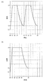
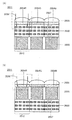
- FIG. 10A and 10B are a flow diagram illustrating an example of a method for manufacturing a sputtering target and a diagram illustrating firing conditions.
- FIG. 6 is a flowchart illustrating an example of a method for manufacturing a sputtering target.
- FIG. 6 is a flowchart illustrating an example of a method for manufacturing a sputtering target.
- FIG. 6 is a flowchart illustrating an example of a method for manufacturing a sputtering target.
- FIG. 6 is a flowchart illustrating an example of a method for manufacturing a sputtering target.
- FIG. 6 is a flowchart illustrating an example of a method for manufacturing a sputtering target.
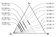
- FIG. 9 is a triangular diagram illustrating a composition of an In—M—Zn oxide.
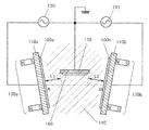
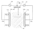
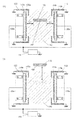
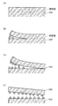
- FIG. 9 illustrates a sputtering apparatus.
- FIG. 9 illustrates a sputtering apparatus.
- FIG. 9 illustrates a sputtering apparatus.
- FIG. 9 illustrates a sputtering apparatus.
- FIG. 9 illustrates a sputtering apparatus.
- the top view which shows an example of the film-forming apparatus.
- FIG. 6 illustrates an example of a structure of a film formation apparatus.
- 8A and 8B illustrate a method for forming a CAAC-OS. Diagram for explaining the crystal and pellets InMZnO 4.
- 8A and 8B illustrate a method for forming a CAAC-OS.
- FIG. 8A and 8B illustrate a method for forming a CAAC-OS.
- 8A and 8B illustrate a method for forming a CAAC-OS.
- 8A and 8B illustrate a method for forming a CAAC-OS.
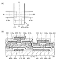
- 4A and 4B are a top view and cross-sectional views of a transistor according to one embodiment of the present invention.
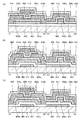
- FIG. 6 is a cross-sectional view of a transistor according to one embodiment of the present invention.
- FIG. 6 is a cross-sectional view of a transistor according to one embodiment of the present invention.
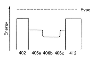
- FIG. 13 is a band diagram of a region including an oxide semiconductor according to one embodiment of the present invention.
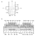
- FIG. 4A and 4B are a top view and cross-sectional views of a transistor according to one embodiment of the present invention.
- FIG. 6 is a cross-sectional view of a transistor according to one embodiment of the present invention.
- FIG. 6 is a cross-sectional view of a transistor according to one embodiment of the present invention.
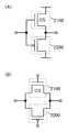
- FIG. 10 is a circuit diagram illustrating a semiconductor device according to one embodiment of the present invention.
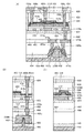
- FIG. 6 is a cross-sectional view illustrating a semiconductor device according to one embodiment of the present invention.
- FIG. 6 is a cross-sectional view illustrating a semiconductor device according to one embodiment of the present invention.
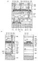
- FIG. 6 is a cross-sectional view illustrating a semiconductor device according to one embodiment of the present invention.
- FIG. 6 is a cross-sectional view illustrating a semiconductor device according to one embodiment of the present invention.
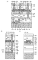
- FIG. 6 is a cross-sectional view illustrating a semiconductor device according to one embodiment of the present invention.
- FIG. 10 is a circuit diagram illustrating a memory device according to one embodiment of the present invention.
- FIG. 6 is a cross-sectional view illustrating a semiconductor device according to one embodiment of the present invention.
- FIG. 6 is a cross-sectional view illustrating a semiconductor device according to one embodiment of the present invention.
- FIG. 6 is a cross-sectional view illustrating a semiconductor device according to one embodiment of the present invention.
- FIG. 6 is a top view illustrating a semiconductor device according to one embodiment of the present invention.
- 1 is a block diagram illustrating a semiconductor device according to one embodiment of the present invention.
- FIG. 6 is a cross-sectional view illustrating a semiconductor device according to one embodiment of the present invention.
- FIG. 6 is a cross-sectional view illustrating a semiconductor device according to one embodiment of the present invention.
- FIG. 6 is a cross-sectional view illustrating a semiconductor device according to one embodiment of the present invention.
- 4A and 4B are a perspective view and a cross-sectional view illustrating a semiconductor device according to one embodiment of the present invention.
- 1 is a block diagram illustrating a semiconductor device according to one embodiment of the present invention.
- FIG. 10 is a circuit diagram illustrating a semiconductor device according to one embodiment of the present invention.
- 4A and 4B are a circuit diagram, a top view, and a cross-sectional view illustrating a semiconductor device according to one embodiment of the present invention.
- FIG. 6 is a cross-sectional view illustrating a semiconductor device according to one embodiment of the present invention.
- FIG. 6A and 6B are a circuit diagram and a cross-sectional view illustrating a semiconductor device according to one embodiment of the present invention.
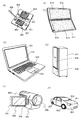
- FIG. 11 is a perspective view illustrating an electronic device according to one embodiment of the present invention.
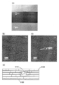
- FIG. 6 is a Cs-corrected high-resolution TEM image in a cross section of a CAAC-OS and a schematic cross-sectional view of the CAAC-OS.
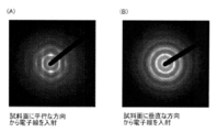
- 6A and 6B illustrate structural analysis by XRD of a CAAC-OS and a single crystal oxide semiconductor. The figure which shows the electron diffraction pattern of CAAC-OS.
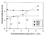
- FIG. 6 shows changes in crystal parts of an In—Ga—Zn oxide due to electron irradiation. The figure which shows hydrogen concentration.
- the voltage indicates a potential difference between a certain potential and a reference potential (for example, a ground potential (GND) or a source potential).
- a voltage can be rephrased as a potential.
- the potential (voltage) is relative and is determined by a relative magnitude from a reference potential. Therefore, even when “ground potential” is described, the potential is not always 0V.
- the lowest potential in the circuit may be the “ground potential”.
- an intermediate potential in the circuit may be a “ground potential”. In that case, a positive potential and a negative potential are defined based on the potential.
- the semiconductor device may have characteristics as an “insulator”.
- the boundary between “semiconductor” and “insulator” is ambiguous and may not be strictly discriminated. Therefore, a “semiconductor” in this specification can be called an “insulator” in some cases.
- an “insulator” in this specification can be called a “semiconductor” in some cases.
- the semiconductor device may have characteristics as a “conductor”.
- the boundary between “semiconductor” and “conductor” is ambiguous, and there are cases where it cannot be strictly distinguished. Therefore, a “semiconductor” in this specification can be called a “conductor” in some cases. Similarly, a “conductor” in this specification can be called a “semiconductor” in some cases.
- the impurity of the semiconductor means, for example, a component other than the main component constituting the semiconductor.
- an element having a concentration of less than 0.1 atomic% is an impurity.
- impurities for example, DOS (Density of State) may be formed in a semiconductor, carrier mobility may be reduced, and crystallinity may be reduced.
- examples of impurities that change the characteristics of the semiconductor include Group 1 elements, Group 2 elements, Group 14 elements, Group 15 elements, and transition metals other than the main component.
- hydrogen also included in water
- lithium, sodium, silicon, boron, phosphorus, carbon, nitrogen and the like are examples of impurities that change the characteristics of the semiconductor.
- oxygen vacancies may be formed by mixing impurities such as hydrogen, for example.
- impurities such as hydrogen, for example.
- examples of impurities that change the characteristics of the semiconductor include group 1 elements, group 2 elements, group 13 elements, and group 15 elements excluding oxygen and hydrogen.
- A has a region having a concentration B
- the concentration in the depth direction in a region with A when it is described that A has a region having a concentration B, for example, when the concentration in the entire depth direction in a region with A is B, the concentration in the depth direction in a region with A
- B when the average value of B is B
- the median value of the concentration in the depth direction in the region of A is B
- the maximum value of the concentration in the depth direction of the region of A there is A
- the concentration in the region where a probable value of A itself is obtained in the measurement. Including the case of B.
- A when A is described as having a region having a size B, a length B, a thickness B, a width B, or a distance B, for example, the entire size and length in a region with A
- the thickness, width, or distance is B
- the average value of the size, length, thickness, width, or distance in a region of A is B
- the size, length in the region of A is When the median value of thickness, thickness, width, or distance is B, when the maximum value of size, length, thickness, width, or distance in a region of A is B, in the region of A Measured when the minimum value of size, length, thickness, width, or distance is B, and when the converged value of size, length, thickness, width, or distance in a region of A is B
- the size, length, thickness, width, or distance in a region where a probable value of A above is obtained is B Case, and the like.
- the channel length refers to, for example, a region where a semiconductor (or a portion where current flows in the semiconductor when the transistor is on) and a gate electrode overlap with each other in a top view of the transistor, or a region where a channel is formed
- the channel length is not necessarily the same in all regions. That is, the channel length of one transistor may not be fixed to one value. Therefore, in this specification, the channel length is any one of values, the maximum value, the minimum value, or the average value in a region where a channel is formed.
- the channel width is, for example, a region in which a semiconductor (or a portion in which a current flows in the semiconductor when the transistor is on) and a gate electrode overlap each other, or a source and a drain in a region where a channel is formed. This is the length of the part. Note that in one transistor, the channel width is not necessarily the same in all regions. That is, the channel width of one transistor may not be fixed to one value. Therefore, in this specification, the channel width is any one of values, the maximum value, the minimum value, or the average value in a region where a channel is formed.
- the channel width in a region where a channel is actually formed (hereinafter referred to as an effective channel width) and the channel width shown in a top view of the transistor (hereinafter, apparent channel width). May be different).
- the effective channel width is larger than the apparent channel width shown in the top view of the transistor, and the influence may not be negligible.
- the ratio of the channel region formed on the side surface of the semiconductor may be large. In that case, the effective channel width in which the channel is actually formed is larger than the apparent channel width shown in the top view.
- an apparent channel width which is a length of a portion where a source and a drain face each other in a region where a semiconductor and a gate electrode overlap with each other in a top view of a transistor is referred to as an “enclosed channel width ( SCW: Surrounded Channel Width).
- SCW Surrounded Channel Width
- channel width in the case where the term “channel width” is simply used, it may denote an enclosed channel width or an apparent channel width.
- channel width in the case where the term “channel width” is simply used, it may denote an effective channel width. Note that the channel length, channel width, effective channel width, apparent channel width, enclosed channel width, and the like can be determined by obtaining a cross-sectional TEM image and analyzing the image. it can.
- the calculation may be performed using the enclosed channel width. In that case, the value may be different from that calculated using the effective channel width.
- A when A is described as having a shape protruding from B, in a top view or a cross-sectional view, it indicates that at least one end of A has a shape that is outside of at least one end of B. There is a case. Therefore, when it is described that A has a shape protruding from B, for example, in a top view, it can be read that one end of A has a shape outside of one end of B.
- parallel refers to a state in which two straight lines are arranged at an angle of ⁇ 10 ° to 10 °. Therefore, the case of ⁇ 5 ° to 5 ° is also included.
- substantially parallel means a state in which two straight lines are arranged at an angle of ⁇ 30 ° to 30 °.
- Vertical refers to a state in which two straight lines are arranged at an angle of 80 ° to 100 °. Therefore, the case of 85 ° to 95 ° is also included.
- substantially vertical means a state in which two straight lines are arranged at an angle of 60 ° to 120 °.
- semiconductor can be read as “oxide semiconductor”.
- Other semiconductors include Group 14 semiconductors such as silicon and germanium, compound semiconductors such as silicon carbide, germanium silicide, gallium arsenide, indium phosphide, zinc selenide, cadmium sulfide, and oxide semiconductors, and organic semiconductors. Can be used.
- oxide can be read as an oxide semiconductor, an oxide insulator, or an oxide conductor.
- ⁇ Target 1> The sputtering target according to one embodiment of the present invention is described below. However, the use of the target is not limited to the sputtering method. For example, it can also be used for a film forming method such as a molecular beam epitaxy (MBE) method or a pulsed laser deposition (PLD) method.
- MBE molecular beam epitaxy
- PLD pulsed laser deposition
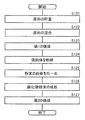
- FIG. 1A is a flowchart illustrating a method for manufacturing a sputtering target.
- the raw materials are weighed (step S101).
- first to nth oxide powders (n is a natural number of 2 or more) are used.
- indium oxide powder, gallium oxide powder, and zinc oxide powder are used.
- tin oxide powder, aluminum oxide powder, titanium oxide powder, nickel oxide powder, zirconium oxide powder, lanthanum oxide powder, cerium oxide powder, neodymium oxide powder, Hafnium oxide powder, tantalum oxide powder or tungsten oxide powder may be used.
- the molar ratio of indium oxide powder, gallium oxide powder and zinc oxide powder is “2: 2: 1”, “8: 4: 3”, “3: 1: 1”, “1: 1: 1”. , “4: 2: 3”, “1: 1: 2”, “3: 1: 4”, “4: 2: 4.1”, “5: 5: 6”, “1: 3: 2” , “1: 3: 4” or “3: 1: 2”.
- the raw materials are not limited to the aforementioned raw materials.
- indium oxide powder, gallium oxide powder, zinc oxide powder, tin oxide powder, aluminum oxide powder, titanium oxide powder, nickel oxide powder, zirconium oxide powder, lanthanum oxide powder, cerium oxide powder, neodymium oxide powder, hafnium oxide powder, Tantalum oxide powder, tungsten oxide powder, indium oxide powder and zinc oxide powder, indium oxide powder and gallium oxide powder, gallium oxide powder and zinc oxide powder, aluminum oxide powder and zinc oxide powder, zinc oxide powder and tin oxide powder, or oxidation Indium powder and tin oxide powder may be used as raw materials.
- the alkali metal can be less than 10 ppm by weight, preferably less than 5 ppm by weight, and more preferably less than 2 ppm by weight.
- the alkaline earth metal can be less than 5 ppm by weight, preferably less than 2 ppm by weight, and more preferably less than 1 ppm by weight.
- each halogen can be less than 10 ppm by weight, preferably less than 5 ppm by weight, and more preferably less than 2 ppm by weight.
- boron, magnesium, phosphorus, copper, and germanium can each be less than 5 ppm by weight, preferably less than 2 ppm by weight, and more preferably less than 1 ppm by weight.
- nitrogen can be less than 20 ppm by weight, preferably less than 10 ppm by weight, more preferably less than 5 ppm by weight, more preferably less than 2 ppm by weight.
- silicon can be less than 50 ppm by weight, preferably less than 20 ppm by weight, more preferably less than 10 ppm by weight, more preferably less than 5 ppm by weight.
- the impurity concentration is determined by secondary ion mass spectrometry (SIMS: Secondary Ion Mass Spectrometry), glow discharge mass spectrometry (GDMS: Glow Discharge Mass Spectrometry) or inductively coupled plasma mass spectrometry (ICP-MS). Measurement may be performed by Spectrometry) or the like.
- SIMS Secondary Ion Mass Spectrometry
- GDMS glow discharge mass spectrometry
- ICP-MS inductively coupled plasma mass spectrometry
- step S102 the weighed raw materials are mixed.
- step S103 the mixed raw materials are spread on a mold and molded.
- the molded body is fired (also referred to as sintering) to produce a sintered body (step S104).
- FIG. 1B is a diagram for explaining firing conditions.
- a furnace also referred to as a firing furnace or a sintering furnace
- Firing starts at time t0 and temperature T1 in an inert atmosphere.
- the temperature T1 may be, for example, 10 ° C. or more and 400 ° C. or less. If the temperature T1 is too high, the furnace members may be deteriorated. On the other hand, if the temperature T1 is too low, it may take a long time to lower the temperature T1 in the subsequent temperature lowering step.
- the inert atmosphere refers to an atmosphere containing an inert gas such as nitrogen or a rare gas or an atmosphere containing no reactive gas such as an oxidizing gas.
- an atmosphere in which a reactive gas such as an oxidizing gas is less than 10%, preferably less than 5%, more preferably less than 1%, more preferably less than 0.1%.
- the pressure in the furnace may be 100 Pa or less, 10 Pa or less, or 1 Pa or less.
- the purity of the inert gas is preferably 8N (99.99999999%) or higher, preferably 9N (99.9999999%) or higher.
- the temperature T2 is, for example, 800 ° C. or higher and 1700 ° C. or lower, preferably 1000 ° C. or higher and 1400 ° C. or lower.
- the time from time t0 to time t1 is, for example, 1 hour to 72 hours, preferably 2 hours to 36 hours, and more preferably 4 hours to 12 hours.
- the temperature may temporarily exceed the temperature T2. In that case, the temperature T2 may be reached after a certain time has elapsed. Therefore, in actual processing, there may be a time during which the temperature becomes higher than the temperature T2, which is the maximum temperature in FIG.
- the temperature T2 is maintained from time t1 to time t3.
- the time from time t1 to time t3 is, for example, 1 hour to 72 hours, preferably 2 hours to 36 hours, and more preferably 4 hours to 12 hours.
- the time from time t1 to time t2 is, for example, 0.5 hours to 70 hours, preferably 1 hour to 30 hours, and more preferably 2 hours to 10 hours.
- the oxidizing atmosphere refers to an atmosphere containing an oxidizing gas.
- the oxidizing gas is oxygen, ozone, nitrous oxide, or the like, and preferably does not contain water, hydrogen, or the like.
- An oxidizing gas and an inert gas may be mixed in the oxidizing atmosphere.
- the atmosphere contains an oxidizing gas of at least 10% or more, preferably 20% or more, more preferably 50% or more, more preferably 90% or more.
- the purity of the oxidizing gas is preferably 8N or higher, preferably 9N or higher.
- the pressure in the furnace may be changed as the atmosphere is switched. For example, the pressure may be increased from atmospheric pressure to atmospheric pressure. Alternatively, the pressure may be reduced from atmospheric pressure.
- the temperature T3 is lowered to a temperature T3 between time t3 and time t4.
- the temperature T3 may be, for example, 20 ° C. or more and 500 ° C. or less. If the temperature T3 is too high, the sintered body may be cracked when taken out from the furnace. If the temperature T3 is too low, it may take a long time to lower the temperature T3.
- firing conditions are not limited to the conditions shown in FIG. For example, you may perform on the conditions shown in FIG. 2 (A) or FIG. 2 (B).
- the firing conditions shown in FIG. 2A start from time t0 and temperature T1 in an inert atmosphere.
- the temperature T1 may be, for example, 10 ° C. or more and 400 ° C. or less. If the temperature T1 is too high, the member may be deteriorated. On the other hand, if the temperature T1 is too low, it may take a long time to lower the temperature T1.
- the pressure in the furnace may be 100 Pa or less, 10 Pa or less, or 1 Pa or less.
- the temperature T2 is, for example, 800 ° C. or higher and 1700 ° C. or lower, preferably 1000 ° C. or higher and 1400 ° C. or lower.
- the time from time t0 to time t1 is, for example, 1 hour to 72 hours, preferably 2 hours to 36 hours, and more preferably 4 hours to 12 hours.
- the time from time t1 to time t3 is, for example, 1 hour to 72 hours, preferably 2 hours to 36 hours, and more preferably 4 hours to 12 hours.
- the time from time t1 to time t2 is, for example, 0.5 hours to 70 hours, preferably 1 hour to 30 hours, and more preferably 2 hours to 10 hours.
- the pressure in the furnace may be changed as the atmosphere is switched. For example, the pressure may be increased from atmospheric pressure to atmospheric pressure. Alternatively, the pressure may be reduced from atmospheric pressure.
- the temperature T3 is lowered to a temperature T3 between time t3 and time t4.
- the temperature T3 may be, for example, 20 ° C. or more and 500 ° C. or less. If the temperature T3 is too low, it may take a long time to lower the temperature T3.
- the atmosphere in the furnace at time t4.
- it may be switched to an inert atmosphere.
- the pressure in the furnace may be changed as the atmosphere is switched.
- the pressure may be increased from atmospheric pressure to atmospheric pressure.
- the pressure may be reduced from atmospheric pressure.
- the temperature is raised to a temperature T2 between time t4 and time t5.
- the time from time t4 to time t5 is, for example, 1 hour to 72 hours, preferably 2 hours to 36 hours, and more preferably 4 hours to 12 hours.
- the temperature may be raised to a temperature different from temperature T2.
- the temperature may be higher than the temperature T2.
- the temperature may be lower than the temperature T2.
- hydrogen and water contained in the sintered body can be more effectively reduced. As a result, the crystallinity of the sintered body can be further increased.
- the temperature T2 is maintained from time t5 to time t7.
- the time from time t5 to time t7 is, for example, 1 hour to 72 hours, preferably 2 hours to 36 hours, and more preferably 4 hours to 12 hours.
- it may be switched to an oxidizing atmosphere.
- the time from time t5 to time t7 may be different from the time from time t1 to time t3.
- the time from time t5 to time t7 may be longer than the time from time t1 to time t3.
- the time from time t5 to time t7 may be shorter than the time from time t1 to time t3.
- the time from time t5 to time t6 is, for example, 0.5 hours or more and 70 hours or less, preferably 1 hour or more and 30 hours or less, and more preferably 2 hours or more and 10 hours or less.
- the time from time t5 to time t6 may be different from the time from time t1 to time t2.
- the time from time t5 to time t6 may be longer than the time from time t1 to time t2.
- the time from time t5 to time t6 may be shorter than the time from time t1 to time t2.
- the pressure in the furnace may be changed as the atmosphere is switched. For example, the pressure may be increased from atmospheric pressure to atmospheric pressure. Alternatively, the pressure may be reduced from atmospheric pressure.
- the temperature is lowered to a temperature T3 between time t7 and time t8.
- the temperature may be lowered to a temperature different from temperature T3.
- the temperature may be higher than the temperature T3.
- the temperature in the furnace is increased and then the temperature is decreased for two cycles.
- the baking according to one embodiment of the present invention is limited to the above conditions. Not. For example, you may repeat 3 cycles or more.
- the temperature to be raised may be increased each time the cycle is repeated. Alternatively, each time the cycle is repeated, the temperature to be raised may be lowered.
- the firing conditions shown in FIG. 2B start at time t0 and temperature T1 in an inert atmosphere.
- the temperature T1 may be, for example, 100 ° C. or more and 400 ° C. or less. If the temperature T1 is too high, the member may be deteriorated. On the other hand, if the temperature T1 is too low, it may take a long time to lower the temperature T1.
- the pressure in the furnace may be 100 Pa or less, 10 Pa or less, or 1 Pa or less.
- the temperature T2 is, for example, 800 ° C. or higher and 1700 ° C. or lower, preferably 1000 ° C. or higher and 1400 ° C. or lower.
- the time from time t0 to time t1 is, for example, 1 hour to 72 hours, preferably 2 hours to 36 hours, and more preferably 4 hours to 12 hours.
- the time from time t1 to time t5 is, for example, 1 hour to 72 hours, preferably 2 hours to 36 hours, and more preferably 4 hours to 12 hours.
- the time from time t1 to time t2 is, for example, 0.5 hours to 70 hours, preferably 1 hour to 30 hours, and more preferably 2 hours to 10 hours.
- the time from time t2 to time t3 is, for example, not less than 0.5 hours and not more than 70 hours, preferably not less than 1 hour and not more than 30 hours, more preferably not less than 2 hours and not more than 10 hours.
- the time from time t3 to time t4 is, for example, 0.5 hours to 70 hours, preferably 1 hour to 30 hours, and more preferably 2 hours to 10 hours.
- the time from time t4 to time t5 is, for example, not less than 0.5 hours and not more than 70 hours, preferably not less than 1 hour and not more than 30 hours, more preferably not less than 2 hours and not more than 10 hours.
- the pressure in the furnace may be changed as the atmosphere is switched. For example, the pressure may be increased from atmospheric pressure to atmospheric pressure. Alternatively, the pressure may be reduced from atmospheric pressure.
- the temperature T3 is lowered to a temperature T3 between time t5 and time t6.
- the temperature T3 may be, for example, 20 ° C. or more and 500 ° C. or less. If the temperature T3 is too low, it may take a long time to lower the temperature T3.
- the temperature in the furnace is increased and then the temperature is decreased for one cycle.
- baking according to one embodiment of the present invention is limited to the above conditions. Not. For example, it may be repeated two or more cycles. Further, the temperature to be raised may be increased each time the cycle is repeated. Alternatively, each time the cycle is repeated, the temperature to be raised may be lowered.
- a sputtering target is manufactured by performing a finishing process on the sintered body that is fired under the above-described conditions and the like. Specifically, in order to adjust the length, width, and thickness of the sintered body, it is divided or ground. In addition, since the surface has minute irregularities, abnormal discharge may occur, so the surface is polished.
- the polishing treatment is preferably performed by chemical mechanical polishing (CMP).
- a sputtering target with a low concentration of impurities such as hydrogen can be manufactured.
- a sputtering target with few oxygen vacancies can be manufactured.
- a sputtering target with high crystallinity can be manufactured.
- a sputtering target having a high relative density can be manufactured. Specifically, the relative density of the sputtering target can be 90% or more, 95% or more, or 99% or more. In addition, the purity of the sputtering target can be increased.
- the ratio of the main component of the sputtering target is 99.9% by weight (3N) or more, preferably 99.99% by weight (4N) or more, more preferably 99.999% by weight (5N) or more. can do.
- Such a sputtering target can be referred to as a high purity intrinsic or substantially high purity intrinsic sputtering target.
- a film with a low impurity concentration can be formed.
- a film with a low hydrogen concentration can be formed.
- a film with few defects can be formed.
- a film with a low carrier density can be formed.
- a highly crystalline film can be formed.
- a film formed using the produced sputtering target is a film according to one embodiment of the present invention.
- An apparatus including a film formed using the produced sputtering target is an apparatus according to one embodiment of the present invention.
- FIG. 3A is a schematic view illustrating a crystal structure of an In-M-Zn oxide.
- In-M-Zn oxide hydrogen atoms that are impurities exist.
- the atomic arrangement is distorted around the site where oxygen deficiency occurs.
- the bond between the adjacent oxygen atom and the indium atom is easily broken due to the distortion of the atomic arrangement.
- the oxygen atom whose bond is broken forms a new OH by bonding a hydrogen atom to an unpaired electron.
- OH OH reaches the surface of the In-M-Zn oxide, it is bonded to another hydrogen atom and desorbed as H 2 O. In this way, oxygen vacancies are further formed.
- the hydrogen concentration decreases.
- oxygen vacancies increase in a chain in one layer (see FIG. 4B).
- heating in an inert atmosphere or under reduced pressure can reduce the hydrogen concentration of the In-M-Zn oxide, but at the same time increase oxygen vacancies. Therefore, it is preferable to perform heating in an oxidizing atmosphere after heating in an inert atmosphere or under reduced pressure.
- oxygen vacancies formed in the In-M-Zn oxide can be reduced.
- the In-M-Zn oxide with reduced oxygen vacancies is obtained when the crystal structure returns to the original crystal structure as shown in FIG. 4C, or when the oxygen atom is lower than the original crystal structure as shown in FIG. The number may increase.
- the In—M—Zn oxide can reduce the hydrogen concentration while maintaining the crystal structure.
- the temperature is lowered in a state where the In-M-Zn oxide contains a large amount of oxygen vacancies, long-time heating may be required to restore the original crystal structure. Therefore, switching from the inert atmosphere or the reduced pressure to the oxidizing atmosphere is preferably performed near the maximum heating temperature.
- VASP Vehicle Ab initio Simulation Package
- PBE Perdew-Burke-Ernzerhof type generalized gradient approximation
- PAW Projector Augmented Wave
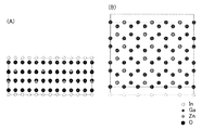
- FIG. 5A and FIG. 5B illustrate an InGaZnO 4 crystal (252 atoms) which is a kind of In-M-Zn oxide.
- FIG. 5A illustrates a structure viewed from a direction perpendicular to the c-axis
- FIG. 5B illustrates a structure viewed from a direction parallel to the c-axis. Note that the frame lines shown in FIGS. 5A and 5B indicate periodic boundaries.
- Model A is a model in which seven oxygen atoms are removed from the layer surrounded by the broken line in FIG. 6A, as shown by the broken line in FIG. 6B. That is, it is a model in which oxygen vacancies are aggregated.
- Model B is a model in which seven oxygen atoms in the dashed-line box shown in FIG. 6D are removed from the layer in the broken-line box in FIG. 6C. That is, in this model, oxygen vacancies exist only in one layer, but are more dispersed than model A.
- Model C is a model in which seven oxygen atoms are randomly removed from the area surrounded by the broken line in FIG. 6E, that is, the entire InGaZnO 4 crystal.
- the model D is a model in which 19 oxygen atoms are removed from the layer surrounded by the broken line in FIG. 7A, as in the broken line illustrated in FIG. 7B. That is, it is a model in which oxygen vacancies are aggregated.
- the model E is a model in which 19 oxygen atoms are removed from the layer surrounded by the broken line in FIG. 7C as in the broken line illustrated in FIG. That is, in this model, oxygen vacancies exist only in one layer, but are more dispersed than model D.
- the model F is a model in which 19 oxygen atoms are randomly removed from the area surrounded by the broken line in FIG. 7E, that is, the entire InGaZnO 4 crystal. That is, this is a model in which oxygen vacancies in InGaZnO 4 crystals are dispersed.
- model A In each of model A, model B, model C, model D, model E, and model F, structure optimization was performed, and the energy of the structure after optimization was calculated. In each model, several arrangements of oxygen vacancies were changed, and the energy of the structure after structure optimization was calculated.
- FIG. 8A shows the energy of the structure after structure optimization in model A, model B, and model C.
- FIG. 8B shows the structure energy after structure optimization in the models D, E, and F.
- FIG. The symbol indicated by a circle is a median value.
- model A had the lowest energy.
- model D has the lowest energy.
- Model A and model D are both models in which oxygen vacancies are aggregated. That is, it can be seen that oxygen vacancies are more stable when aggregated than dispersed when the numbers are the same.
- FIG. 9 is a flowchart showing a method for manufacturing a sputtering target.
- the raw materials are weighed (step S111).
- first to nth oxide powders (n is a natural number of 2 or more) are used.
- indium oxide powder, gallium oxide powder, and zinc oxide powder are used.
- tin oxide powder, aluminum oxide powder, titanium oxide powder, nickel oxide powder, zirconium oxide powder, lanthanum oxide powder, cerium oxide powder, neodymium oxide powder, Hafnium oxide powder, tantalum oxide powder or tungsten oxide powder may be used.
- the molar ratio of indium oxide powder, gallium oxide powder and zinc oxide powder is “2: 2: 1”, “8: 4: 3”, “3: 1: 1”, “1: 1: 1”. , “4: 2: 3”, “1: 1: 2”, “3: 1: 4”, “4: 2: 4.1”, “5: 5: 6”, “1: 3: 2” , “1: 3: 4” or “3: 1: 2”.
- the raw materials are not limited to the aforementioned raw materials.
- indium oxide powder, gallium oxide powder, zinc oxide powder, tin oxide powder, aluminum oxide powder, titanium oxide powder, nickel oxide powder, zirconium oxide powder, lanthanum oxide powder, cerium oxide powder, neodymium oxide powder, hafnium oxide powder, Tantalum oxide powder, tungsten oxide powder, indium oxide powder and zinc oxide powder, indium oxide powder and gallium oxide powder, gallium oxide powder and zinc oxide powder, aluminum oxide powder and zinc oxide powder, zinc oxide powder and tin oxide powder, or oxidation Indium powder and tin oxide powder may be used as raw materials.
- step S112 the weighed raw material, water, and organic substances (dispersant and binder) are mixed to form a slurry.
- the slurry is poured into the mold (step S113).
- One or a plurality of suction ports are provided at the bottom of the mold so that water or the like can be sucked.
- a filter is provided at the bottom of the mold.
- the filter has a function of passing water and organic matter without passing through the raw material powder. Specifically, a filter in which a porous resin film is attached on a woven fabric or felt may be used.
- the molded body is formed by sucking water and the like through the filter provided at the bottom of the mold and removing water and organic substances from the slurry (step S114).
- a molded body in which the raw material is uniformly mixed can be formed.
- step S115 a drying process and removal of organic substance are performed (step S115). It is preferable that the drying process is performed by natural drying because the molded body is difficult to crack. In addition, by performing heat treatment at a temperature of 300 ° C. or higher and 700 ° C. or lower, water and organic matter that cannot be removed during natural drying can be removed.
- a sintered compact is produced by baking a molded object (step S116). Note that the firing may be performed under the conditions described in FIG. 1B, FIG. 2A, or FIG.
- a sputtering target is produced by performing a finishing process on the produced sintered body. Specifically, in order to adjust the length, width, and thickness of the sintered body, it is divided or ground. In addition, since the surface has minute irregularities, abnormal discharge may occur, so the surface is polished.
- the polishing treatment is preferably performed by CMP.
- a sputtering target with a low concentration of impurities such as hydrogen can be manufactured.
- a sputtering target with few oxygen vacancies can be manufactured.
- a sputtering target with high crystallinity can be manufactured.
- the raw materials can be uniformly mixed at the time of forming the molded body, a sputtering target having a higher relative density can be produced.
- a film with a low impurity concentration can be formed.
- a film with a low hydrogen concentration can be formed.
- a film with few defects can be formed.
- a film with a low carrier density can be formed.
- a highly crystalline film can be formed.
- a film formed using the produced sputtering target is a film according to one embodiment of the present invention.
- An apparatus including a film formed using the produced sputtering target is an apparatus according to one embodiment of the present invention.
- FIG. 10 is a flowchart showing a method for manufacturing a sputtering target.
- the raw materials are weighed (step S121).
- first to nth oxide powders (n is a natural number of 2 or more) are used.
- indium oxide powder, gallium oxide powder, and zinc oxide powder are used.
- tin oxide powder, aluminum oxide powder, titanium oxide powder, nickel oxide powder, zirconium oxide powder, lanthanum oxide powder, cerium oxide powder, neodymium oxide powder, Hafnium oxide powder, tantalum oxide powder or tungsten oxide powder may be used.
- the molar ratio of indium oxide powder, gallium oxide powder and zinc oxide powder is “2: 2: 1”, “8: 4: 3”, “3: 1: 1”, “1: 1: 1”. , “4: 2: 3”, “1: 1: 2”, “3: 1: 4”, “4: 2: 4.1”, “5: 5: 6”, “1: 3: 2” , “1: 3: 4” or “3: 1: 2”.
- the raw materials are not limited to the aforementioned raw materials.
- indium oxide powder, gallium oxide powder, zinc oxide powder, tin oxide powder, aluminum oxide powder, titanium oxide powder, nickel oxide powder, zirconium oxide powder, lanthanum oxide powder, cerium oxide powder, neodymium oxide powder, hafnium oxide powder, Tantalum oxide powder, tungsten oxide powder, indium oxide powder and zinc oxide powder, indium oxide powder and gallium oxide powder, gallium oxide powder and zinc oxide powder, aluminum oxide powder and zinc oxide powder, zinc oxide powder and tin oxide powder, or oxidation Indium powder and tin oxide powder may be used as raw materials.
- step S122 the weighed raw materials are mixed.
- step S123 the mixed raw materials are fired.
- the first baking may be performed under the conditions described in FIG. 1B, FIG. 2A, or FIG.
- an oxide which is a reactive organism of the mixed raw material is obtained.
- an In—Ga—Zn oxide is obtained. Note that the first baking may be performed a plurality of times under different conditions.
- the In—Ga—Zn oxide powder is pulverized to obtain crystalline In—Ga—Zn oxide powder (step S124).
- a pulverizer such as a ball mill may be used for pulverization of the In—Ga—Zn oxide.
- a material having high hardness such as agate, aluminum oxide, zirconium oxide, tungsten carbide, or silicon carbide may be used.
- the container used for the ball mill is not particularly limited, it is preferable to use the same material as the above-mentioned ball.
- the pulverization by the ball mill may be performed for 8 hours or more and 72 hours or less, preferably 20 hours or more and 72 hours or less.
- step S124 the process may return to step S123 to perform first baking on the In—Ga—Zn oxide powder.
- the In—Ga—Zn oxide is pulverized again in step S124 after the first baking.
- the particle diameter of the obtained In—Ga—Zn oxide powder is made uniform (step S125).
- the treatment is performed so that the particle diameter of the In—Ga—Zn oxide powder is 1 ⁇ m or less, preferably 0.5 ⁇ m or less, and more preferably 0.3 ⁇ m or less.
- a sieve or a filter that allows passage of particles of 1 ⁇ m or less, 0.5 ⁇ m or less, or 0.3 ⁇ m or less may be used. After that, it is preferable to remove In—Ga—Zn oxide powder having a particle size of less than 0.01 ⁇ m, which often has low crystallinity.
- the particle diameter of the In—Ga—Zn oxide powder can be 0.01 ⁇ m or more and 1 ⁇ m or less, 0.01 ⁇ m or more and 0.5 ⁇ m or less, or 0.01 ⁇ m or more and 0.3 ⁇ m or less.
- step S126 the In—Ga—Zn oxide is spread over a mold and molded.
- step S127 the molded body is fired (second firing) to produce a sintered body.
- the second baking may be performed under the conditions described in FIG. 1B, FIG. 2A, or FIG.
- a sputtering target is produced by performing a finishing process on the produced sintered body. Specifically, in order to adjust the length, width, and thickness of the sintered body, it is divided or ground. In addition, since the surface has minute irregularities, abnormal discharge may occur, so the surface is polished.
- the polishing treatment is preferably performed by CMP.
- a sputtering target with a low concentration of impurities such as hydrogen can be manufactured.
- a sputtering target with few oxygen vacancies can be manufactured.
- the oxide powder contained in the compact has high crystallinity, a sputtering target with higher crystallinity can be manufactured.
- a sputtering target having a high relative density can be manufactured.
- a film with a low impurity concentration can be formed.
- a film with a low hydrogen concentration can be formed.
- a film with few defects can be formed.
- a film with a low carrier density can be formed.
- a highly crystalline film can be formed.
- a film formed using the produced sputtering target is a film according to one embodiment of the present invention.
- An apparatus including a film formed using the produced sputtering target is an apparatus according to one embodiment of the present invention.
- FIG. 11 is a flowchart showing a method for manufacturing a sputtering target.
- the raw materials are weighed (step S131).
- first to nth oxide powders (n is a natural number of 2 or more) are used.
- indium oxide powder, gallium oxide powder, and zinc oxide powder are used.
- tin oxide powder, aluminum oxide powder, titanium oxide powder, nickel oxide powder, zirconium oxide powder, lanthanum oxide powder, cerium oxide powder, neodymium oxide powder, Hafnium oxide powder, tantalum oxide powder or tungsten oxide powder may be used.
- the molar ratio of indium oxide powder, gallium oxide powder and zinc oxide powder is “2: 2: 1”, “8: 4: 3”, “3: 1: 1”, “1: 1: 1”. , “4: 2: 3”, “1: 1: 2”, “3: 1: 4”, “4: 2: 4.1”, “5: 5: 6”, “1: 3: 2” , “1: 3: 4” or “3: 1: 2”.
- the raw materials are not limited to the aforementioned raw materials.
- indium oxide powder, gallium oxide powder, zinc oxide powder, tin oxide powder, aluminum oxide powder, titanium oxide powder, nickel oxide powder, zirconium oxide powder, lanthanum oxide powder, cerium oxide powder, neodymium oxide powder, hafnium oxide powder, Tantalum oxide powder, tungsten oxide powder, indium oxide powder and zinc oxide powder, indium oxide powder and gallium oxide powder, gallium oxide powder and zinc oxide powder, aluminum oxide powder and zinc oxide powder, zinc oxide powder and tin oxide powder, or oxidation Indium powder and tin oxide powder may be used as raw materials.
- step S132 the weighed raw materials are mixed.
- step S133 the mixed raw materials are fired.
- the first baking may be performed under the conditions described in FIG. 1B, FIG. 2A, or FIG.
- an oxide which is a reactive organism of the mixed raw material is obtained.
- an In—Ga—Zn oxide is obtained. Note that the first baking may be performed a plurality of times under different conditions.
- an In—Ga—Zn oxide powder having crystallinity is obtained by pulverizing the In—Ga—Zn oxide (step S134).
- a pulverizer such as a ball mill may be used for pulverization of the In—Ga—Zn oxide.
- a material having high hardness such as agate, aluminum oxide, zirconium oxide, tungsten carbide, or silicon carbide may be used.
- the container used for the ball mill is not particularly limited, it is preferable to use the same material as the above-mentioned ball.
- the pulverization by the ball mill may be performed for 8 hours or more and 72 hours or less, preferably 20 hours or more and 72 hours or less.
- step S134 the process may return to step S133 to perform first baking on the In—Ga—Zn oxide powder.
- the In—Ga—Zn oxide is pulverized again in step S134 after the first baking.
- the particle diameter of the obtained In—Ga—Zn oxide powder is made uniform (step S135).
- the treatment is performed so that the particle diameter of the In—Ga—Zn oxide powder is 1 ⁇ m or less, preferably 0.5 ⁇ m or less, and more preferably 0.3 ⁇ m or less.
- a sieve or a filter that allows passage of particles of 1 ⁇ m or less, 0.5 ⁇ m or less, or 0.3 ⁇ m or less may be used. After that, it is preferable to remove In—Ga—Zn oxide powder having a particle size of less than 0.01 ⁇ m, which often has low crystallinity.
- the particle diameter of the In—Ga—Zn oxide powder can be 0.01 ⁇ m or more and 1 ⁇ m or less, 0.01 ⁇ m or more and 0.5 ⁇ m or less, or 0.01 ⁇ m or more and 0.3 ⁇ m or less.
- step S136 the In—Ga—Zn oxide, water, and organic substances (dispersant and binder) are mixed to form a slurry.
- the slurry is poured into the mold (step S137).
- One or a plurality of suction ports are provided at the bottom of the mold so that water or the like can be sucked.
- a filter is provided at the bottom of the mold.
- the filter has a function of passing water and organic matter without passing through the raw material powder. Specifically, a filter in which a porous resin film is attached on a woven fabric or felt may be used.
- step S138 the slurry is sucked through a filter provided at the bottom of the mold, and water and organic substances are removed from the slurry, thereby forming a molded body.
- step S139 a drying process and removal of organic substance are performed (step S139). It is preferable that the drying process is performed by natural drying because the molded body is difficult to crack. In addition, by performing heat treatment at a temperature of 300 ° C. or higher and 700 ° C. or lower, water and organic matter that cannot be removed during natural drying can be removed.
- a sintered compact is produced by baking (2nd baking) a molded object (step S140).
- the second baking may be performed under the conditions described in FIG. 1B, FIG. 2A, or FIG.
- a sputtering target is produced by performing a finishing process on the produced sintered body. Specifically, in order to adjust the length, width, and thickness of the sintered body, it is divided or ground. In addition, since the surface has minute irregularities, abnormal discharge may occur, so the surface is polished.
- the polishing treatment is preferably performed by CMP.
- a sputtering target with a low concentration of impurities such as hydrogen can be manufactured.
- a sputtering target with few oxygen vacancies can be manufactured.
- the oxide powder contained in the compact has high crystallinity, a sputtering target with higher crystallinity can be manufactured.
- the raw materials can be uniformly mixed at the time of forming the molded body, a sputtering target having a higher relative density can be produced.
- a film with a low impurity concentration can be formed.
- a film with a low hydrogen concentration can be formed.
- a film with few defects can be formed.
- a film with a low carrier density can be formed.
- a highly crystalline film can be formed.
- a film formed using the produced sputtering target is a film according to one embodiment of the present invention.
- An apparatus including a film formed using the produced sputtering target is an apparatus according to one embodiment of the present invention.
- composition> a composition of an In-M-Zn oxide that can be used for a sputtering target will be described.
- the element M is aluminum, gallium, yttrium, tin, or the like.
- Other elements applicable to the element M include boron, silicon, titanium, iron, nickel, germanium, zirconium, molybdenum, lanthanum, cerium, neodymium, hafnium, tantalum, and tungsten.
- FIG. 12 is a triangular diagram in which In, M, or Zn is arranged at each vertex.
- [In] indicates the atomic concentration of In
- [M] indicates the atomic concentration of the element M
- [Zn] indicates the atomic concentration of Zn.
- a crystal of In-M-Zn oxide is known to have a homologous structure, and is represented by InMO 3 (ZnO) m (m is a natural number).
- InMO 3 (ZnO) m m is a natural number.
- In 1 + ⁇ M 1- ⁇ O 3 (ZnO) m can be used.
- the thick line on the broken line is a composition that can be a solid solution when, for example, an oxide as a raw material is mixed and fired at 1350 ° C.
- the crystallinity can be increased by bringing the composition close to the above-mentioned solid solution.
- the composition of the target and the composition of the film may be different.
- the atomic ratio is “1: 1: 1”, “1: 1: 1.2”, “3: 1: 2”, “4: 2: 4.1”, “1: 3: 2”.
- a target composition may be selected in consideration of a change in composition.
- a sputtering apparatus in which the sputtering target according to one embodiment of the present invention can be installed is described.
- the sputtering apparatus described below is illustrated with a substrate, a target, and the like in order to facilitate understanding or to explain operations during film formation.
- the substrate, the target, and the like are objects that a user installs in a normal sputtering apparatus, and thus the sputtering apparatus according to one embodiment of the present invention may not have the substrate and the target.
- FIG. 13A is a cross-sectional view of a film formation chamber 101 which is a parallel plate sputtering apparatus.
- a deposition chamber 101 illustrated in FIG. 13A includes a target holder 120, a backing plate 110, a target 100, a magnet unit 130, and a substrate holder 170.
- the target 100 is disposed on the backing plate 110. Further, the backing plate 110 is disposed on the target holder 120.
- the magnet unit 130 is disposed under the target 100 via the backing plate 110. Further, the substrate holder 170 is disposed to face the target 100.
- a combination of a plurality of magnets is called a magnet unit.
- the magnet unit can be called a cathode, a cathode magnet, a magnetic member, a magnetic component, or the like.
- the magnet unit 130 includes a magnet 130N, a magnet 130S, and a magnet holder 132. In the magnet unit 130, the magnet 130N and the magnet 130S are disposed on the magnet holder 132. Further, the magnet 130N is arranged at a distance from the magnet 130S. Note that when the substrate 160 is carried into the film formation chamber 101, the substrate 160 is disposed on the substrate holder 170.
- the film-forming method using the parallel plate type sputtering apparatus can also be called PESP (parallel electrode SP).
- the target holder 120 and the backing plate 110 are fixed using screws (bolts or the like) and are equipotential. Further, the target holder 120 has a function of supporting the target 100 via the backing plate 110.
- the target 100 is fixed to the backing plate 110.
- the backing plate 110 and the target 100 can be fixed by a bonding material containing a low melting point metal such as indium.
- FIG. 13A shows magnetic force lines 180 a and magnetic force lines 180 b formed by the magnet unit 130.
- the magnetic force line 180 a is one of magnetic force lines that form a horizontal magnetic field in the vicinity of the upper surface of the target 100.
- the vicinity of the upper surface of the target 100 is, for example, a region having a vertical distance from the target 100 of 0 mm to 10 mm, particularly 0 mm to 5 mm.
- the magnetic force line 180b is one of the magnetic force lines that form a horizontal magnetic field at a vertical distance d from the upper surface of the magnet unit 130.
- the vertical distance d is, for example, 0 mm or more and 20 mm or less, or 5 mm or more and 15 mm or less.
- a strong magnetic field can be generated near the top surface of the substrate 160 by using the strong magnet 130N and the strong magnet 130S.
- the magnetic flux density of the horizontal magnetic field on the upper surface of the substrate 160 can be set to 10G to 100G, preferably 15G to 60G, and more preferably 20G to 40G.
- the measurement of the magnetic flux density of a horizontal magnetic field should just measure the value when the magnetic flux density of a vertical magnetic field is 0G.
- the magnetic flux density in the film formation chamber 101 By setting the magnetic flux density in the film formation chamber 101 within the above range, an oxide with high density and high crystallinity can be formed.
- the obtained oxide hardly contains a plurality of types of crystal phases, and becomes an oxide containing almost a single crystal phase.
- FIG. 13B shows a top view of the magnet unit 130.
- a circular or substantially circular magnet 130 ⁇ / b> N and a circular or substantially circular magnet 130 ⁇ / b> S are fixed to the magnet holder 132.
- the magnet unit 130 can be rotated using the center or substantially center normal vector on the upper surface of the magnet unit 130 as a rotation axis.
- the magnet unit 130 may be rotated at a beat of 0.1 Hz to 1 kHz (in other words, rhythm, time signature, pulse, frequency, period, or cycle).
- the strong magnetic field region on the target 100 changes as the magnet unit 130 rotates. Since the region having a strong magnetic field is a high-density plasma region, the sputtering phenomenon of the target 100 tends to occur in the vicinity thereof. For example, when a region having a strong magnetic field is a specific location, only a specific region of the target 100 is used. On the other hand, by rotating the magnet unit 130 as shown in FIG. 13B, the target 100 can be used uniformly. Further, by rotating the magnet unit 130, a film having a uniform thickness and a uniform quality can be formed.
- the direction of the lines of magnetic force on the upper surface of the substrate 160 can be changed.
- the magnet unit 130 may be swung up and down or / and left and right.
- the magnet unit 130 may be moved with a beat of 0.1 Hz to 1 kHz.
- the target 100 may be rotated or moved.
- the target 100 may be rotated or moved with a beat of 0.1 Hz to 1 kHz.
- the direction of the lines of magnetic force on the upper surface of the substrate 160 may be relatively changed by rotating the substrate 160. Or you may combine these.
- the film formation chamber 101 may have a water channel inside or below the backing plate 110. Then, by flowing a fluid (air, nitrogen, rare gas, water, oil, etc.) through the water channel, discharge abnormality due to a rise in the temperature of the target 100 during sputtering, damage to the film formation chamber 101 due to deformation of members, and the like are suppressed. be able to. At this time, it is preferable that the backing plate 110 and the target 100 are brought into close contact with each other through a bonding material because cooling performance is improved.
- a fluid air, nitrogen, rare gas, water, oil, etc.
- a gasket be provided between the target holder 120 and the backing plate 110 because impurities are unlikely to enter the film formation chamber 101 from the outside or a water channel.
- the magnet 130N and the magnet 130S are arranged with different poles facing the target 100 side.
- the magnet 130N is arranged so that the target 100 side has an N pole
- the magnet 130S is arranged so that the target 100 side has an S pole.
- the arrangement of magnets and poles in the magnet unit 130 is not limited to this arrangement. Further, the arrangement is not limited to that shown in FIG.
- the potential V1 applied to the terminal V1 connected to the target holder 120 is lower than the potential V2 applied to the terminal V2 connected to the substrate holder 170, for example.
- the potential V2 applied to the terminal V2 connected to the substrate holder 170 is, for example, a ground potential.
- the potential V3 applied to the terminal V3 connected to the magnet holder 132 is, for example, a ground potential.
- the potential applied to the terminal V1, the terminal V2, and the terminal V3 is not limited to the above potential.
- the potential may not be applied to all of the target holder 120, the substrate holder 170, and the magnet holder 132.
- the substrate holder 170 may be electrically floating. Note that FIG.
- FIG. 13A illustrates an example of a so-called DC sputtering method in which the potential V1 is applied to the terminal V1 connected to the target holder 120; however, one embodiment of the present invention is not limited thereto.
- a so-called RF sputtering method in which a high frequency power source having a frequency of 13.56 MHz or 27.12 MHz is connected to the target holder 120 may be used.
- FIG. 13A shows an example in which the backing plate 110 and the target holder 120 are not electrically connected to the magnet unit 130 and the magnet holder 132, but the present invention is not limited to this.
- the backing plate 110 and the target holder 120, and the magnet unit 130 and the magnet holder 132 are electrically connected and may be equipotential.
- the temperature of the substrate 160 may be increased in order to further increase the crystallinity of the obtained oxide.
- the temperature of the substrate 160 may be, for example, 100 ° C to 450 ° C, preferably 150 ° C to 400 ° C, and more preferably 170 ° C to 350 ° C.
- the deposition gas can be a rare gas such as argon (in addition to helium, neon, krypton, xenon). Etc.) and oxygen are preferably used.
- the proportion of oxygen in the whole may be less than 50% by volume, preferably 33% by volume or less, more preferably 20% by volume or less, more preferably 15% by volume or less.
- the vertical distance between the target 100 and the substrate 160 is 10 mm to 600 mm, preferably 20 mm to 400 mm, more preferably 30 mm to 200 mm, and more preferably 40 mm to 100 mm.
- a decrease in energy before the sputtered particles reach the substrate 160 may be suppressed.
- the incident direction of the sputtered particles to the substrate 160 can be made closer to the vertical, so that the damage to the substrate 160 due to the collision of the sputtered particles is reduced. Sometimes it can be made smaller.
- FIG. 14A illustrates an example of a deposition chamber which is different from that in FIG.
- a deposition chamber 101 illustrated in FIG. 14A includes a target holder 120a, a target holder 120b, a backing plate 110a, a backing plate 110b, a target 100a, a target 100b, a magnet unit 130a, and a magnet unit 130b. , A member 142 and a substrate holder 170.
- the target 100a is disposed on the backing plate 110a.
- the backing plate 110a is disposed on the target holder 120a.
- the magnet unit 130a is arrange
- the target 100b is disposed on the backing plate 110b.
- the backing plate 110b is disposed on the target holder 120b.
- the magnet unit 130b is arrange
- the magnet unit 130a includes a magnet 130N1, a magnet 130N2, a magnet 130S, and a magnet holder 132.
- magnet 130N1, magnet 130N2, and magnet 130S are arranged on magnet holder 132. Further, the magnet 130N1 and the magnet 130N2 are arranged with a gap from the magnet 130S.
- the magnet unit 130b has the same structure as the magnet unit 130a. Note that when the substrate 160 is carried into the film formation chamber 101, the substrate 160 is disposed on the substrate holder 170.
- the target 100a, the backing plate 110a and the target holder 120a are separated from the target 100b, the backing plate 110b and the target holder 120b by a member 142.
- the member 142 is preferably an insulator.
- the member 142 may be a conductor or a semiconductor.
- the member 142 may be a conductor or semiconductor whose surface is covered with an insulator.
- the target holder 120a and the backing plate 110a are fixed using screws (bolts or the like) and are equipotential. Further, the target holder 120a has a function of supporting the target 100a via the backing plate 110a. Further, the target holder 120b and the backing plate 110b are fixed using screws (bolts or the like) and are equipotential. Further, the target holder 120b has a function of supporting the target 100b via the backing plate 110b.
- the backing plate 110a has a function of fixing the target 100a.
- the backing plate 110b has a function of fixing the target 100b.
- FIG. 14A shows magnetic lines of force 180a and magnetic lines of force 180b formed by the magnet unit 130a.
- the magnetic force line 180a is one of the magnetic force lines that form a horizontal magnetic field in the vicinity of the upper surface of the target 100a.
- the vicinity of the upper surface of the target 100a is, for example, an area having a vertical distance from the target 100a of 0 mm to 10 mm, particularly 0 mm to 5 mm.
- the magnetic force line 180b is one of magnetic force lines that form a horizontal magnetic field at a vertical distance d from the upper surface of the magnet unit 130a.
- the vertical distance d is, for example, 0 mm or more and 20 mm or less, or 5 mm or more and 15 mm or less.
- a strong magnetic field can be generated even in the vicinity of the upper surface of the substrate 160 by using the strong magnet 130N1, the magnet 130N2, and the strong magnet 130S.
- the magnetic flux density of the horizontal magnetic field on the upper surface of the substrate 160 can be set to 10G to 100G, preferably 15G to 60G, and more preferably 20G to 40G.
- the magnetic flux density of the magnetic field in the deposition chamber 101 By setting the magnetic flux density of the magnetic field in the deposition chamber 101 within the above range, an oxide with high density and high crystallinity can be formed.
- the obtained oxide hardly contains a plurality of types of crystal phases, and becomes an oxide containing almost a single crystal phase.
- the magnet unit 130b also has the same magnetic lines as the magnet unit 130a.
- FIG. 14B shows a top view of the magnet unit 130a and the magnet unit 130b.
- the magnet unit 130a it can be seen that a rectangular or substantially rectangular magnet 130N1, a rectangular or substantially rectangular magnet 130N2, and a rectangular or substantially rectangular magnet 130S are fixed to the magnet holder 132. Then, the magnet unit 130a can be swung left and right as shown in FIG. For example, the magnet unit 130a may be swung with a beat of 0.1 Hz to 1 kHz.
- the region with a strong magnetic field on the target 100a changes as the magnet unit 130a swings. Since the region having a strong magnetic field becomes a high-density plasma region, the sputtering phenomenon of the target 100a tends to occur in the vicinity thereof. For example, when a region having a strong magnetic field is a specific location, only a specific region of the target 100a is used. On the other hand, as shown in FIG. 14B, the target 100a can be used uniformly by swinging the magnet unit 130a. Further, by swinging the magnet unit 130a, a film having a uniform thickness and quality can be formed.
- the state of the magnetic lines of force on the upper surface of the substrate 160 can be changed by swinging the magnet unit 130a. The same applies to the magnet unit 130b.
- the magnet unit 130a and the magnet unit 130b may be rotated.
- the magnet unit 130a and the magnet unit 130b may be rotated at a cycle of 0.1 Hz to 1 kHz.
- the target 100 may be rotated or moved.
- the target 100 may be rotated or moved at a cycle of 0.1 Hz to 1 kHz.
- the state of the lines of magnetic force on the upper surface of the substrate 160 can be relatively changed by rotating the substrate 160. Alternatively, these may be combined.
- the film formation chamber 101 may have a water channel inside or below the backing plate 110a and the backing plate 110b. Then, by causing a fluid (air, nitrogen, rare gas, water, oil, etc.) to flow through the water channel, discharge abnormality due to a rise in the temperature of the target 100a and the target 100b during sputtering, damage to the film formation chamber 101 due to deformation of members, and the like. Can be suppressed.
- a fluid air, nitrogen, rare gas, water, oil, etc.
- the backing plate 110a and the target 100a are in close contact with each other through a bonding material because the cooling performance is improved. Further, it is preferable that the backing plate 110b and the target 100b are in close contact with each other through a bonding material because the cooling performance is improved.
- a gasket be provided between the target holder 120 a and the backing plate 110 a because impurities are unlikely to enter the film formation chamber 101 from the outside or a water channel.
- the magnet 130N1, the magnet 130N2, and the magnet 130S are arranged with different poles facing the target 100a.
- the magnet 130N1 and the magnet 130N2 are arranged so that the target 100a side has an N pole
- the magnet 130S is arranged so that the target 100a side has an S pole.
- the arrangement of magnets and poles in the magnet unit 130a is not limited to this arrangement. Further, the arrangement is not limited to that shown in FIG. The same applies to the magnet unit 103b.
- the potential V2 applied to the terminal V2 connected to the substrate holder 170 is, for example, a ground potential.
- the potential V3 applied to the terminal V3 connected to the magnet holder 132 is, for example, a ground potential.
- the potential applied to the terminal V1, the terminal V2, the terminal V3, and the terminal V4 is not limited to the above potential. Further, the potential may not be applied to all of the target holder 120a, the target holder 120b, the substrate holder 170, and the magnet holder 132.
- the substrate holder 170 may be electrically floating.
- FIG. 14A an example of a so-called AC sputtering method in which a potential that alternates between high and low is applied between the terminal V1 connected to the target holder 120a and the terminal V4 connected to the target holder 120b. Although shown, one embodiment of the present invention is not limited thereto.
- the backing plate 110a and the target holder 120a are not electrically connected to the magnet unit 130a and the magnet holder 132, but the present invention is not limited to this.
- the backing plate 110a and the target holder 120a, and the magnet unit 130a and the magnet holder 132 are electrically connected, and may be equipotential.
- the backing plate 110b and the target holder 120b are not electrically connected to the magnet unit 130b and the magnet holder 132 has been shown, the present invention is not limited to this.
- the backing plate 110a and the target holder 120b, the magnet unit 130b, and the magnet holder 132 are electrically connected, and may be equipotential.
- the temperature of the substrate 160 may be increased in order to further increase the crystallinity of the obtained oxide.
- the temperature of the substrate 160 may be, for example, 100 ° C to 450 ° C, preferably 150 ° C to 400 ° C, and more preferably 170 ° C to 350 ° C.
- the deposition gas can be a rare gas such as argon (in addition to helium, neon, krypton, xenon). Etc.) and oxygen are preferably used.
- the proportion of oxygen in the whole may be less than 50% by volume, preferably 33% by volume or less, more preferably 20% by volume or less, more preferably 15% by volume or less.
- the vertical distance between the target 100a and the substrate 160 is 10 mm to 600 mm, preferably 20 mm to 400 mm, more preferably 30 mm to 200 mm, more preferably 40 mm to 100 mm.
- a decrease in energy before the sputtered particles reach the substrate 160 may be suppressed.
- the incident direction of the sputtered particles to the substrate 160 can be made closer to the vertical, so that the damage to the substrate 160 due to the collision of the sputtered particles is reduced. Sometimes it can be made smaller.
- the vertical distance between the target 100b and the substrate 160 is 10 mm to 600 mm, preferably 20 mm to 400 mm, more preferably 30 mm to 200 mm, more preferably 40 mm to 100 mm.
- a decrease in energy before the sputtered particles reach the substrate 160 may be suppressed.
- the incident direction of the sputtered particles on the substrate 160 can be made closer to the vertical, so that damage to the substrate 160 due to the collision of the sputtered particles can be reduced. Sometimes it can be made smaller.
- FIG. 15A illustrates an example of a cross-sectional view of a deposition chamber which is different from those in FIGS. 13A and 14A.
- FIG. 15A illustrates an opposed target sputtering apparatus.
- a film formation method using an opposed target sputtering apparatus can also be referred to as VDSP (vapor deposition SP).
- FIG. 15A is a schematic cross-sectional view of a film formation chamber in a sputtering apparatus.
- the deposition chamber illustrated in FIG. 15A includes a target 100a and a target 100b, a backing plate 110a and a backing plate 110b that hold the target 100a and the target 100b, respectively, and the target 100a and the backing plate 110b via the backing plate 110a and the backing plate 110b.
- the magnet unit 130a and the magnet unit 130b are respectively disposed on the back surface of the target 100b.
- the substrate holder 170 is disposed between the target 100a and the target 100b. Note that when the substrate 160 is placed in the deposition chamber, the substrate 160 is fixed by the substrate holder 170.
- a power source 190 and a power source 191 for applying a potential are connected to the backing plate 110a and the backing plate 110b. It is preferable to use a so-called AC power source that applies a potential at which the potential is alternately switched between a power source 190 connected to the backing plate 110a and a power source 191 connected to the backing plate 110b.
- the power supply 190 and the power supply 191 shown in FIG. 15 have shown the example using AC power supply, it is not restricted to this.
- an RF power source, a DC power source, or the like may be used as the power source 190 and the power source 191.
- different types of power sources may be used for the power source 190 and the power source 191.
- the substrate holder 170 is preferably connected to the GND. Further, the substrate holder 170 may be in a floating state.
- FIG. 15B and 15C illustrate the potential distribution of the plasma 140 between the alternate long and short dash line A-B in FIG.
- the potential distribution shown in FIG. 15B shows a state in which a high potential is applied to the backing plate 110a and a low potential is applied to the backing plate 110b. That is, positive ions are accelerated toward the target 100b.
- the potential distribution shown in FIG. 15C shows a state in which a low potential is applied to the backing plate 110a and a high potential is applied to the backing plate 110b. That is, positive ions are accelerated toward the target 100b.
- Film formation can be performed so that the states of FIG. 15B and FIG. 15C are alternately switched.
- a film with the plasma 140 sufficiently reaching the surface of the substrate 160.
- FIG. 15A a state where the substrate holder 170 and the substrate 160 are arranged in the plasma 140 is preferable.
- the substrate holder 170 and the substrate 160 be disposed in the positive column region in the plasma 140.
- the positive column region in the plasma 140 is a region where the gradient of the potential distribution is small in the potential distributions shown in FIGS. 15B and 15C. That is, as shown in FIG. 15A, the substrate 160 is not exposed to the strong electric field portion under the plasma 140 by disposing the substrate 160 in the positive column region in the plasma 140, so that the substrate 160 is damaged by the plasma 140. Therefore, defects can be reduced.
- FIG. 15A it is preferable to form a film in a state where the substrate holder 170 and the substrate 160 are arranged in the plasma 140 because the use efficiency of the target 100a and the target 100b is increased.
- the horizontal distance between the substrate holder 170 and the target 100a is L1
- the horizontal distance between the substrate holder 170 and the target 100b is L2.
- the lengths L1 and L2 are preferably the same length as the substrate 160, respectively.
- L1 and L2 may be 10 mm or more and 200 mm or less, respectively.
- the target 100a and the target 100b are arranged to face each other in parallel. Further, the magnet unit 130a and the magnet unit 130b are arranged so that different poles face each other. At this time, the lines of magnetic force are directed from the magnet unit 130b to the magnet unit 130a. Therefore, at the time of film formation, the plasma 140 is confined in the magnetic field formed by the magnet unit 130a and the magnet unit 130b.
- the substrate holder 170 and the substrate 160 are disposed in a region (also referred to as an inter-target region) between the target 100a and the target 100b facing each other. In FIG.
- the substrate holder 170 and the substrate 160 are arranged in parallel to the direction in which the target 100a and the target 100b face each other, but they may be arranged at an angle. For example, by tilting the substrate holder 170 and the substrate 160 by 30 ° or more and 60 ° or less (typically 45 °), the proportion of sputtered particles that are perpendicularly incident on the substrate 160 during film formation can be increased.
- the configuration shown in FIG. 16 is different from the configuration shown in FIG. 15A in that the target 100a and the target 100b are not parallel but are arranged to face each other in an inclined state (in a V shape). Therefore, the description of FIG. 15A is referred to except for the arrangement of the target. Further, the magnet unit 130a and the magnet unit 130b are arranged so that different poles face each other. The substrate holder 170 and the substrate 160 are arranged in the inter-target region. By arranging the target 100a and the target 100b as shown in FIG. 16, the ratio of sputtered particles reaching the substrate 160 increases, so that the deposition rate can be increased.
- FIG. 15A shows a state in which the substrate holder 170 and the substrate 160 are arranged in the plasma 140, but the present invention is not limited to this.
- the substrate holder 170 and the substrate 160 may be disposed outside the plasma 140. Since the substrate 160 is not exposed to the high electric field region of the plasma 140, damage due to the plasma 140 can be reduced. However, the use efficiency of the target 100a and the target 100b decreases as the substrate 160 is separated from the plasma 140. Further, it is preferable that the position of the substrate holder 170 is variable as shown in FIG.
- the substrate holder 170 is disposed on the upper side of the inter-target region, it may be disposed on the lower side. Moreover, you may arrange
- the facing target sputtering apparatus can stably generate plasma even in a high vacuum. For example, film formation is possible even at 0.005 Pa or more and 0.09 Pa or less. Therefore, the concentration of impurities mixed during film formation can be reduced.
- the facing target sputtering apparatus By using the facing target sputtering apparatus, film formation at high vacuum is possible, so that a film with high crystallinity can be formed even when the temperature of the substrate 160 is low. For example, even when the temperature of the substrate 160 is 10 ° C. or higher and lower than 100 ° C., a highly crystalline film can be formed.
- FIG. 18A illustrates another example of a counter target sputtering apparatus.
- FIG. 18A is a schematic cross-sectional view of a film formation chamber in an opposed target sputtering apparatus. Unlike the film formation chamber shown in FIG. 15A, a target shield 122 and a target shield 123 are provided. Moreover, it has the power supply 191 connected with the backing plate 110a and the backing plate 110b.
- the target shield 122a and the target shield 122b are connected to GND. That is, the plasma 140 is formed by the potential difference applied between the backing plate 110a and the backing plate 110b to which the potential of the power source 191 is applied and the target shield 122a and the target shield 122b to which GND is applied.
- the substrate holder 170 and the substrate 160 are disposed in the plasma 140.
- the substrate holder 170 and the substrate 160 be disposed in the positive column region in the plasma 140.
- the positive column region in the plasma is a region where the gradient of the potential distribution is small. That is, as shown in FIG. 18A, the substrate 160 is not exposed to the strong electric field portion under the plasma 140 by disposing the substrate 160 in the positive column region in the plasma 140, so that the substrate 160 is not damaged by the plasma 140. Less oxide with good film quality can be obtained.
- the film with the substrate holder 170 and the substrate 160 placed in the plasma 140 as shown in FIG. 18A because the use efficiency of the target 100a and the target 100b is increased.
- the horizontal distance between the substrate holder 170 and the target 100a is L1
- the horizontal distance between the substrate holder 170 and the target 100b is L2.
- the lengths of L1 and L2 are each preferably equal to the size of the substrate 160.
- the present invention is not limited to this.
- the substrate holder 170 and the substrate 160 may be disposed outside the plasma 140. Since the substrate 160 is not exposed to the high electric field region of the plasma 140, damage due to the plasma 140 can be reduced. However, the use efficiency of the target 100a and the target 100b decreases as the substrate 160 is separated from the plasma 140. Further, it is preferable that the position of the substrate holder 170 be variable as shown in FIG.
- the substrate holder 170 is arranged on the upper side of the region where the target 100a and the target 100b face each other, but may be arranged on the lower side. Moreover, you may arrange
- the counter target sputtering apparatus described above can reduce plasma damage to the substrate because the plasma is confined to the magnetic field between the targets. Further, since the incident angle of the sputtered particles on the substrate can be made shallow by the inclination of the target, the step coverage of the deposited film can be improved. In addition, since film formation in a high vacuum is possible, the concentration of impurities mixed in the film can be reduced.
- a parallel plate sputtering apparatus or an ion beam sputtering apparatus may be applied to the film formation chamber.
- FIG. 19 schematically shows a top view of a single-wafer multi-chamber film forming apparatus 2700.
- the film formation apparatus 2700 includes an atmosphere-side substrate supply chamber 2701 that includes a cassette port 2761 that accommodates a substrate and an alignment port 2762 that aligns the substrate, and an atmosphere-side substrate that transports the substrate from the atmosphere-side substrate supply chamber 2701.
- an unload lock chamber 2703b for switching from atmospheric pressure to reduced pressure a transfer chamber 2704 for transferring a substrate in a vacuum, a substrate heating chamber 2705 for heating the substrate, and a film formation chamber 2706a for forming a film with a target disposed.
- a film formation chamber 2706b and a film formation chamber 2706c Note that the above-described structure of the film formation chamber can be referred to for the film formation chamber 2706a, the film formation chamber 2706b, and the film formation chamber 2706c.
- the atmosphere-side substrate transfer chamber 2702 is connected to the load lock chamber 2703a and the unload lock chamber 2703b, the load lock chamber 2703a and the unload lock chamber 2703b are connected to the transfer chamber 2704, and the transfer chamber 2704 is heated to the substrate.
- the chamber 2705, the film formation chamber 2706a, the film formation chamber 2706b, and the film formation chamber 2706c are connected.
- a gate valve 2764 is provided at a connection portion of each chamber, and each chamber can be kept in a vacuum state independently of the atmosphere-side substrate supply chamber 2701 and the atmosphere-side substrate transfer chamber 2702.
- the atmosphere-side substrate transfer chamber 2702 and the transfer chamber 2704 have a transfer robot 2763 and can transfer a substrate.
- the substrate heating chamber 2705 is preferably used also as a plasma processing chamber.
- the film formation apparatus 2700 can transport the substrate between the processes without being exposed to the atmosphere, and thus can suppress the adsorption of impurities to the substrate.
- the order of film formation and heat treatment can be established freely. Note that the number of transfer chambers, film formation chambers, load lock chambers, unload lock chambers, and substrate heating chambers is not limited to the above-described numbers, and an optimal number can be provided as appropriate in accordance with installation space and process conditions.
- FIG. 20 shows a cross section corresponding to one-dot chain line X1-X2, one-dot chain line Y1-Y2, and one-dot chain line Y2-Y3 shown in FIG.
- FIG. 20A illustrates a cross section of the substrate heating chamber 2705 and the transfer chamber 2704.
- the substrate heating chamber 2705 includes a plurality of heating stages 2765 that can accommodate substrates.
- the substrate heating chamber 2705 is connected to a vacuum pump 2770 through a valve.
- a vacuum pump 2770 for example, a dry pump, a mechanical booster pump, or the like can be used.
- a heating mechanism that can be used for the substrate heating chamber 2705 for example, a heating mechanism that heats using a resistance heating element or the like may be used.
- a heating mechanism that heats by heat conduction or heat radiation from a medium such as a heated gas may be used.
- RTA Rapid Thermal Anneal
- GRTA Rapid Thermal Anneal
- LRTA Heats an object to be processed by radiation of light (electromagnetic waves) emitted from a lamp such as a halogen lamp, a metal halide lamp, a xenon arc lamp, a carbon arc lamp, a high pressure sodium lamp, or a high pressure mercury lamp.
- GRTA performs heat treatment using a high-temperature gas. An inert gas is used as the gas.
- the substrate heating chamber 2705 is connected to a purifier 2781 via a mass flow controller 2780.
- the mass flow controller 2780 and the purifier 2781 are provided as many as the number of gas types, but only one is shown for easy understanding.
- a gas having a dew point of ⁇ 80 ° C. or lower, preferably ⁇ 100 ° C. or lower can be used.
- oxygen gas, nitrogen gas, and rare gas (such as argon gas) can be used. Use.
- the transfer chamber 2704 has a transfer robot 2863.
- the transfer robot 2763 can transfer a substrate to each chamber.
- the transfer chamber 2704 is connected to a vacuum pump 2770 and a cryopump 2771 through valves. With such a configuration, the transfer chamber 2704 is evacuated using a vacuum pump 2770 from atmospheric pressure to low vacuum or medium vacuum (about 0.1 to several hundred Pa), and the valve is switched to switch from medium vacuum to high vacuum. A vacuum or ultra-high vacuum (0.1 Pa to 1 ⁇ 10 ⁇ 7 Pa) is exhausted using a cryopump 2771.
- cryopumps 2771 may be connected in parallel to the transfer chamber 2704. With such a configuration, even if one cryopump is being regenerated, the remaining cryopump can be used to exhaust.
- the regeneration mentioned above refers to the process which discharge
- FIG. 20B illustrates a cross section of the deposition chamber 2706b, the transfer chamber 2704, and the load lock chamber 2703a.
- a film formation chamber 2706b illustrated in FIG. 20B includes a target 2766a, a target 2766b, a target shield 2767a, a target shield 2767b, a magnet unit 2790a, a magnet unit 2790b, a substrate holder 2768, a power supply 2791, Have Although not shown, the target 2766a and the target 2766b are each fixed to a target holder via a backing plate. A power source 2791 is electrically connected to the target 2766a and the target 2766b. Magnet unit 2790a and magnet unit 2790b are arranged on the back of target 2766a and target 2766b, respectively.
- Target shield 2767a and target shield 2767b are arranged to surround the ends of target 2766a and target 2766b, respectively.
- a substrate 2769 is supported by the substrate holder 2768.
- the substrate holder 2768 is fixed to the film formation chamber 2706b through the variable member 2784.
- the variable member 2784 the substrate holder 2768 can be moved to an area between the targets 2766a and 2766b (also referred to as an inter-target area).
- the substrate holder 2768 may include a substrate holding mechanism that holds the substrate 2769, a back heater that heats the substrate 2769 from the back surface, and the like.
- the target shield 2767a and the target shield 2767b can suppress deposition of particles sputtered from the target 2766a and the target 2766b in unnecessary regions.
- the target shield 2767 and the target shield 2767b are preferably processed so that the accumulated sputtered particles do not peel off.
- the surface of the target shield 2767 and the target shield 2767b may be provided with unevenness by increasing the surface roughness.
- the film formation chamber 2706b is connected to the mass flow controller 2780 via the gas heating mechanism 2782, and the gas heating mechanism 2784 is connected to the purifier 2781 via the mass flow controller 2780.
- the gas introduced into the film formation chamber 2706b can be heated to 40 ° C. or higher and 400 ° C. or lower, preferably 50 ° C. or higher and 200 ° C. or lower by the gas heating mechanism 2782.
- the gas heating mechanism 2782, the mass flow controller 2780, and the purifier 2781 are provided as many as the number of gas types, but only one is shown for easy understanding.
- a gas having a dew point of ⁇ 80 ° C. or lower, preferably ⁇ 100 ° C. or lower can be used.
- oxygen gas, nitrogen gas, and a rare gas (such as argon gas) are used. Use.
- the length of the pipe from the purifier to the film formation chamber 2706b is 10 m or less, preferably 5 m or less, and more preferably 1 m or less.
- the length of the pipe is 10 m or less, 5 m or less, or 1 m or less.
- a metal pipe whose inside is covered with iron fluoride, aluminum oxide, chromium oxide or the like may be used for the gas pipe.
- the above-described piping has a smaller amount of gas containing impurities compared to, for example, SUS316L-EP piping, and can reduce the entry of impurities into the gas.
- UPG joint ultra-small metal gasket joint
- the pipes are all made of metal, because the influence of the generated released gas and external leakage can be reduced as compared with the case where resin or the like is used.
- the film formation chamber 2706b is connected to a turbo molecular pump 2772 and a vacuum pump 2770 through valves.
- the film formation chamber 2706b is provided with a cryotrap 2751.
- the cryotrap 2751 is a mechanism that can adsorb molecules (or atoms) having a relatively high melting point such as water.
- the turbo molecular pump 2772 stably exhausts large-sized molecules (or atoms) and has a low maintenance frequency, so that it is excellent in productivity, but has a low exhaust capability of hydrogen or water. Therefore, a cryotrap 2751 is connected to the film formation chamber 2706b in order to increase the exhaust capability of water or the like.
- the temperature of the cryotrap 2751 refrigerator is 100K or less, preferably 80K or less. Further, in the case where the cryotrap 2751 has a plurality of refrigerators, it is preferable to change the temperature for each refrigerator because exhaust can be efficiently performed.
- the temperature of the first stage refrigerator may be 100K or less, and the temperature of the second stage refrigerator may be 20K or less.
- a higher vacuum can be achieved by using a titanium sublimation pump instead of the cryotrap.
- an even higher vacuum can be achieved by using an ion pump instead of the cryopump or the turbo molecular pump.
- the exhaust method of the film formation chamber 2706b is not limited thereto, and a structure similar to the exhaust method (exhaust method of a cryopump and a vacuum pump) described in the above transfer chamber 2704 may be employed.
- the evacuation method of the transfer chamber 2704 may have a configuration similar to that of the film formation chamber 2706b (evacuation method using a turbo molecular pump and a vacuum pump).
- the back pressure (total pressure) of the transfer chamber 2704, the substrate heating chamber 2705, and the film formation chamber 2706b, and the partial pressure of each gas molecule (atom) are preferably as follows.
- impurities may be mixed into the formed film, it is necessary to pay attention to the back pressure of the film formation chamber 2706b and the partial pressure of each gas molecule (atom).
- the back pressure (total pressure) of each chamber described above is 1 ⁇ 10 ⁇ 4 Pa or less, preferably 3 ⁇ 10 ⁇ 5 Pa or less, and more preferably 1 ⁇ 10 ⁇ 5 Pa or less.
- the partial pressure of gas molecules (atoms) having a mass-to-charge ratio (m / z) of 18 in each chamber described above is 3 ⁇ 10 ⁇ 5 Pa or less, preferably 1 ⁇ 10 ⁇ 5 Pa or less, more preferably 3 ⁇ . 10 ⁇ 6 Pa or less.
- the partial pressure of the gas molecule (atom) whose m / z of each chamber is 28 is 3 ⁇ 10 ⁇ 5 Pa or less, preferably 1 ⁇ 10 ⁇ 5 Pa or less, more preferably 3 ⁇ 10 ⁇ 6.
- the partial pressure of the gas molecule (atom) whose m / z of each chamber is 44 is 3 ⁇ 10 ⁇ 5 Pa or less, preferably 1 ⁇ 10 ⁇ 5 Pa or less, more preferably 3 ⁇ 10 ⁇ 6. Pa or less.
- the total pressure and partial pressure in a vacuum chamber can be measured using a mass spectrometer.
- a mass spectrometer also referred to as Q-mass
- Q-mass Qulee CGM-051 manufactured by ULVAC, Inc.
- the transfer chamber 2704, the substrate heating chamber 2705, and the film formation chamber 2706b described above preferably have a structure with little external or internal leakage.
- the leakage rate of the transfer chamber 2704, the substrate heating chamber 2705, and the film formation chamber 2706b described above is 3 ⁇ 10 ⁇ 6 Pa ⁇ m 3 / s or less, preferably 1 ⁇ 10 ⁇ 6 Pa ⁇ m 3 / s or less. It is.
- the leak rate of gas molecules (atoms) having an m / z of 18 is 1 ⁇ 10 ⁇ 7 Pa ⁇ m 3 / s or less, preferably 3 ⁇ 10 ⁇ 8 Pa ⁇ m 3 / s or less.
- the leak rate of gas molecules (atoms) having an m / z of 28 is 1 ⁇ 10 ⁇ 5 Pa ⁇ m 3 / s or less, preferably 1 ⁇ 10 ⁇ 6 Pa ⁇ m 3 / s or less. Further, the leak rate of gas molecules (atoms) having an m / z of 44 is 3 ⁇ 10 ⁇ 6 Pa ⁇ m 3 / s or less, preferably 1 ⁇ 10 ⁇ 6 Pa ⁇ m 3 / s or less.
- the leak rate may be derived from the total pressure and partial pressure measured using the mass spectrometer described above.
- the leak rate depends on the external leak and the internal leak.
- An external leak is a gas flowing from outside the vacuum system due to a minute hole or a seal failure.
- the internal leak is caused by leakage from a partition such as a valve in the vacuum system or gas released from an internal member. In order to make the leak rate below the above-mentioned numerical value, it is necessary to take measures from both the external leak and the internal leak.
- the open / close portion of the film formation chamber 2706b may be sealed with a metal gasket.
- the metal gasket is preferably a metal covered with iron fluoride, aluminum oxide, or chromium oxide.
- Metal gaskets have higher adhesion than O-rings and can reduce external leakage.
- emission gas containing impurities released from the metal gasket can be suppressed, and internal leakage can be reduced.
- aluminum, chromium, titanium, zirconium, nickel, or vanadium that emits less impurities and contains less impurities is used as a member that forms the film formation apparatus 2700.
- the above-described member may be used by being coated with an alloy containing iron, chromium, nickel and the like. Alloys containing iron, chromium, nickel, etc. are rigid, heat resistant and suitable for processing.
- the surface irregularities of the member are reduced by polishing or the like in order to reduce the surface area, the emitted gas can be reduced.
- the member of the film formation apparatus 2700 described above may be covered with iron fluoride, aluminum oxide, chromium oxide, or the like.
- the member of the film forming apparatus 2700 is preferably made of only metal as much as possible.
- the surface is made of iron fluoride, aluminum oxide, It is good to coat thinly with chromium oxide.
- the adsorbate present in the film forming chamber does not affect the pressure in the film forming chamber because it is adsorbed on the inner wall or the like, but causes gas emission when the film forming chamber is exhausted. Therefore, although there is no correlation between the leak rate and the exhaust speed, it is important to desorb the adsorbate present in the film formation chamber as much as possible and exhaust it in advance using a pump having a high exhaust capability.
- the deposition chamber may be baked to promote desorption of the adsorbate. Baking can increase the desorption rate of the adsorbate by about 10 times. Baking may be performed at 100 ° C to 450 ° C.
- the desorption rate of water or the like that is difficult to desorb only by exhausting can be further increased.
- the desorption rate of the adsorbate can be further increased.
- oxygen or the like may be used instead of the inert gas.
- an inert gas such as a heated rare gas or oxygen
- the deposition chamber it is preferable to perform a process of increasing the pressure in the deposition chamber by introducing an inert gas such as a heated rare gas or oxygen, and exhausting the deposition chamber again after a predetermined time.
- an inert gas such as a heated rare gas or oxygen
- the adsorbate in the deposition chamber can be desorbed, and impurities present in the deposition chamber can be reduced.
- this treatment is repeated 2 times or more and 30 times or less, preferably 5 times or more and 15 times or less.
- an inert gas or oxygen having a temperature of 40 ° C. or higher and 400 ° C. or lower, preferably 50 ° C. or higher and 200 ° C.
- the pressure in the deposition chamber is 0.1 Pa or higher and 10 kPa or lower, preferably The pressure may be 1 Pa or more and 1 kPa or less, more preferably 5 Pa or more and 100 Pa or less, and the period for maintaining the pressure may be 1 minute or more and 300 minutes or less, preferably 5 minutes or more and 120 minutes or less.
- the film formation chamber is evacuated for a period of 5 minutes to 300 minutes, preferably 10 minutes to 120 minutes.
- the desorption rate of the adsorbate can be further increased by performing dummy film formation.
- Dummy film formation is performed by depositing a film on the dummy substrate by sputtering or the like, thereby depositing a film on the dummy substrate and the inner wall of the film forming chamber, and depositing impurities on the film forming chamber and adsorbed material on the inner wall of the film forming film. It means confining inside.
- the dummy substrate is preferably a substrate that emits less gas. By performing dummy film formation, the impurity concentration in a film to be formed later can be reduced.
- the dummy film formation may be performed simultaneously with baking.
- FIG. 20C illustrates a cross section of the atmosphere-side substrate transfer chamber 2702 and the atmosphere-side substrate supply chamber 2701.
- the load lock chamber 2703 a has a substrate transfer stage 2752.
- the load lock chamber 2703a raises the pressure from the reduced pressure state to the atmosphere, and when the pressure in the load lock chamber 2703a reaches the atmospheric pressure, the transfer robot 2763 provided in the atmosphere side substrate transfer chamber 2702 moves to the substrate transfer stage 2752. Receive the board. After that, the load lock chamber 2703a is evacuated to a reduced pressure state, and then the transfer robot 2762 provided in the transfer chamber 2704 receives the substrate from the substrate transfer stage 2752.
- the load lock chamber 2703a is connected to a vacuum pump 2770 and a cryopump 2771 through valves. Since the connection method of the exhaust system of the vacuum pump 2770 and the cryopump 2771 can be connected by referring to the connection method of the transfer chamber 2704, description thereof is omitted here. Note that the unload lock chamber 2703b shown in FIG. 19 can have the same configuration as the load lock chamber 2703a.
- the atmosphere-side substrate transfer chamber 2702 has a transfer robot 2763.
- the transfer robot 2763 can transfer the substrate between the cassette port 2761 and the load lock chamber 2703a. Further, a mechanism for cleaning dust or particles such as a HEPA filter (High Efficiency Particulate Air Filter) may be provided above the atmosphere side substrate transfer chamber 2702 and the atmosphere side substrate supply chamber 2701.
- HEPA filter High Efficiency Particulate Air Filter
- the atmosphere side substrate supply chamber 2701 has a plurality of cassette ports 2761.
- the cassette port 2761 can accommodate a plurality of substrates.
- the target has a surface temperature of 100 ° C. or lower, preferably 50 ° C. or lower, more preferably about room temperature (typically 25 ° C.).
- a large area target is often used.
- a large number of targets are arranged side by side with as little gap as possible, but a slight gap is inevitably generated. From such a slight gap, the surface temperature of the target is increased, so that zinc and the like are volatilized, and the gap may gradually widen.
- the backing plate or the metal of the bonding material used for joining the backing plate and the target may be sputtered, which increases the impurity concentration. Therefore, it is preferable that the target is sufficiently cooled.
- a metal specifically, copper having high conductivity and high heat dissipation is used as the backing plate.
- a target can be efficiently cooled by forming a water channel in the backing plate and flowing a sufficient amount of cooling water through the water channel.
- the target contains zinc
- plasma damage is reduced, and an oxide that hardly causes volatilization of zinc can be obtained.
- the hydrogen concentration is 2 ⁇ 10 20 atoms / cm 3 or less, preferably 5 ⁇ 10 19 atoms / cm 3 in secondary ion mass spectrometry (SIMS).
- SIMS secondary ion mass spectrometry
- an oxide semiconductor with a thickness of 1 ⁇ 10 19 atoms / cm 3 or less, more preferably 5 ⁇ 10 18 atoms / cm 3 or less can be formed.
- the nitrogen concentration in SIMS is less than 5 ⁇ 10 19 atoms / cm 3 , preferably 1 ⁇ 10 19 atoms / cm 3 or less, more preferably 5 ⁇ 10 18 atoms / cm 3 or less, and further preferably 1 ⁇ 10 9.
- An oxide semiconductor with a density of 18 atoms / cm 3 or less can be formed.
- the carbon concentration in SIMS is less than 5 ⁇ 10 19 atoms / cm 3 , preferably 5 ⁇ 10 18 atoms / cm 3 or less, more preferably 1 ⁇ 10 18 atoms / cm 3 or less, and even more preferably 5 ⁇ 10.
- An oxide semiconductor with a density of 17 atoms / cm 3 or less can be formed.
- a gas molecule (atom) in which m / z is 2 (such as a hydrogen molecule) by a temperature desorption gas spectroscopy (TDS) analysis
- TDS temperature desorption gas spectroscopy
- the release amount of gas molecules (atoms) with / z of 28 and gas molecules (atoms) with m / z of 44 is 1 ⁇ 10 19 pieces / cm 3 or less, preferably 1 ⁇ 10 18 pieces / cm 3, respectively.
- the following oxide semiconductor can be formed.
- a distance d between the substrate 220 and the target 230 (also referred to as a target-substrate distance (T-S distance)) is 0.01 m or more and 1 m or less, preferably 0.02 m or more and 0.5 m or less.
- the film formation chamber is mostly filled with a film forming gas (for example, oxygen, argon, or a mixed gas containing oxygen at a ratio of 5% by volume or more), and is 0.01 Pa to 100 Pa, preferably 0.1 Pa to 10 Pa. Controlled.
- a film forming gas for example, oxygen, argon, or a mixed gas containing oxygen at a ratio of 5% by volume or more
- a high-density plasma region is formed near the target 230 by a magnetic field.
- ions 201 are generated by ionizing the deposition gas.
- the ion 201 is, for example, an oxygen cation (O + ) or an argon cation (Ar + ).
- a heating mechanism 260 is provided below the substrate 220.
- the target 230 is bonded to the backing plate 210.
- a magnet 250 is disposed at a position facing the target 230 via the backing plate 210.
- a sputtering method that uses a magnetic field to increase the deposition rate is called a magnetron sputtering method.
- the target 230 has a polycrystalline structure having a plurality of crystal grains, and any one of the crystal grains includes a cleavage plane.
- FIG. 22A illustrates a crystal structure of InMZnO 4 (the element M is, for example, aluminum, gallium, yttrium, or tin) included in the target 230.
- FIG. 22A illustrates a crystal structure of InMZnO 4 when observed from a direction parallel to the b-axis.
- a repulsive force is generated between two adjacent M—Zn—O layers because the oxygen atom has a negative charge. Therefore, the InMZnO 4 crystal has a cleavage plane between two adjacent M—Zn—O layers.
- the ions 201 generated in the high-density plasma region are accelerated to the target 230 side by the electric field and eventually collide with the target 230.
- the pellet 200 that is a sputtered particle in the form of a flat plate or pellet is peeled off from the cleavage plane.
- the particles 203 are also ejected from the target 230 as the pellet 200 is peeled off.
- the particle 203 has an aggregate of one atom or several atoms. Therefore, the particle 203 can also be referred to as atomic particles.
- FIG. 23A is a cross-sectional view of the target 230 having a cleavage plane (broken line portion).
- the bond starts to break from the end of the cleavage plane (see FIG. 23B).
- the cleaved surfaces repel each other due to the presence of charges of the same polarity. Therefore, recombination does not occur at the point where the bond is once broken. Then, as the repulsion due to the charge progresses, the disconnected region gradually expands (see FIG. 23C). Eventually, the pellet 200 peels from the target 230 (see FIG. 23D).
- the pellet 200 is a portion sandwiched between two cleavage planes shown in FIG. Therefore, when only the pellet 200 is extracted, the cross section becomes as shown in FIG. 22B and the upper surface becomes as shown in FIG. 22C. Note that the pellet 200 may be distorted in structure due to the impact of the collision of the ions 201.
- the pellet 200 is a flat or pellet-like sputtered particle having a triangular plane, for example, a regular triangular plane.
- the pellet 200 is a flat or pellet-like sputtered particle having a hexagonal plane, for example, a regular hexagonal plane.
- the shape of the pellet 200 is not limited to a triangle or a hexagon.
- the thickness of the pellet 200 is determined according to the type of deposition gas.
- the pellet 200 has a thickness of 0.4 nm to 1 nm, preferably 0.6 nm to 0.8 nm.
- the pellet 200 has a width of 1 nm to 3 nm, preferably 1.2 nm to 2.5 nm.
- the pellet 200 may be charged negatively or positively by receiving a charge from the plasma 240.
- the pellet 200 may receive a negative charge from O 2 ⁇ present in the plasma 240. In that case, oxygen atoms on the surface of the pellet 200 are negatively charged. Further, the pellet 200 may grow laterally when the particles 203 adhere to the side surfaces in the plasma 240 and are bonded.
- the pellets 200 and the particles 203 that have passed through the plasma 240 reach the surface of the substrate 220. Note that some of the particles 203 may be discharged to the outside by a vacuum pump or the like because of a small mass.
- a pellet 200 a that is the first pellet 200 is deposited on the substrate 220. Since the pellet 200a has a flat plate shape, it is deposited with the plane side facing the surface of the substrate 220 (see FIG. 24A). At this time, the charge on the surface of the pellet 200 a on the substrate 220 side is released through the substrate 220.
- the pellet 200 b which is the second pellet 200 reaches the substrate 220. At this time, since the surface of the pellet 200a and the surface of the pellet 200b are charged, forces that repel each other are generated (see FIG. 24B).
- the pellet 200b is deposited with the plane side facing away from the surface of the substrate 220, avoiding the pellet 200a (see FIG. 24C).
- innumerable pellets 200 are deposited on the surface of the substrate 220 by a thickness corresponding to one layer. Further, a region where the pellet 200 is not deposited is generated between the pellet 200 and another pellet 200.
- a pellet 200c which is the third pellet 200, is deposited on the surface of the substrate 220 with the plane side facing. Then, the particles 203 that receive energy from the plasma 240 reach the surface of the substrate 220 (see FIG. 25A).
- the particles 203 cannot be deposited in an active area such as the surface of the pellet 200. Therefore, the particles 203 are deposited so as to fill a region where the pellet 200 is not deposited. And the particle
- FIG. 25B When the bond 203 is activated by the energy received from the plasma 240, the particle 203 is chemically connected to the pellet 200 to form the lateral growth portion 202 (see FIG. 25B). Further, the lateral growth portion 202 grows in the lateral direction (also referred to as lateral growth), whereby the pellets 200 are connected to form a layer 206a (see FIG. 25C). In this way, the particles 203 are accumulated until the non-deposited region of the pellet 200 is filled. This mechanism is similar to the deposition mechanism of the atomic layer deposition (ALD) method.
- ALD atomic layer deposition
- the particles 203 are filled with the particles 203 while laterally growing. A clear crystal grain boundary is not formed.
- the particles 203 are smoothly connected between the plurality of pellets 200, a crystal structure different from single crystal and polycrystal is formed. In other words, a crystal structure having a strain between minute crystal regions (pellets 200) is formed. As described above, since the region between the crystal regions is a distorted crystal region, it is considered inappropriate to refer to the region as an amorphous structure.
- pellets 206d, pellets 206e, and pellets 206f which are new pellets 200, are deposited with the plane side facing the surface of the layer 206a (see FIG. 26A).
- the particles 203 are deposited so as to fill a region where the pellet 200 is not deposited.
- the particles 203 adhere to the side surfaces of the pellet 200 and the laterally grown portion 202 grows laterally, thereby connecting the pellets 200 and forming a layer 206b (see FIG. 26B).
- the film formation continues until the m-th layer (m is an integer of 2 or more) 206m is formed, and a thin film structure having a stacked body is obtained (see FIG. 26C).
- the manner in which the pellets 200 are deposited also varies depending on the surface temperature of the substrate 220 and the like.
- the pellet 200 causes migration on the surface of the substrate 220.
- the proportion of the pellet 200 and another pellet 200 that are connected without the particle 203 is increased, so that the CAAC-OS with high orientation is obtained.
- the surface temperature of the substrate 220 in forming the CAAC-OS is 100 ° C. or higher and lower than 500 ° C., preferably 140 ° C. or higher and lower than 450 ° C., more preferably 170 ° C. or higher and lower than 400 ° C. Therefore, even when a large-area substrate of the eighth generation or higher is used as the substrate 220, it is found that almost no warpage or the like due to the formation of the CAAC-OS film occurs.
- the pellet 200 when the surface temperature of the substrate 220 is low, the pellet 200 is less likely to cause migration on the surface of the substrate 220. As a result, the pellets 200 are stacked to form an nc-OS (nanocrystalline oxide semiconductor) with low orientation. In the nc-OS, since the pellet 200 is negatively charged, the pellet 200 may be deposited at a predetermined interval. Therefore, although the orientation is low, a slight regularity results in a dense structure as compared with an amorphous oxide semiconductor.
- nc-OS nanocrystalline oxide semiconductor
- one large pellet may be formed when the gap between pellets is extremely small.
- the inside of one large pellet has a single crystal structure.
- the size of the pellet may be 10 nm to 200 nm, 15 nm to 100 nm, or 20 nm to 50 nm when viewed from above.
- the pellets are deposited on the surface of the substrate by the film formation model as described above. Since the CAAC-OS film can be formed even when the formation surface does not have a crystal structure, it can be seen that the above-described film formation model, which is a growth mechanism different from epitaxial growth, has high validity. Further, since the above-described film formation model is used, it can be seen that the CAAC-OS and the nc-OS can form a uniform film even on a large-area glass substrate or the like. For example, the CAAC-OS can be formed even when the surface (formation surface) of the substrate has an amorphous structure (eg, amorphous silicon oxide).
- amorphous structure eg, amorphous silicon oxide
- the following may be performed in order to form a highly crystalline CAAC-OS.
- the film is formed in a higher vacuum state.
- the plasma energy is weakened.
- thermal energy is applied to the surface to be formed, and the plasma damage is cured each time the film is formed.
- the pellet is flat.
- the pellet reaching the surface of the substrate is deposited in various directions.
- grains adhere to a side surface with the direction which each deposited, and a lateral growth part raise
- the crystal orientation in the obtained thin film may not be uniform.
- the above-described deposition model has a polycrystalline structure of a complex oxide such as an In-M-Zn oxide in which the target has a plurality of crystal grains, and any one of the crystal grains includes a cleavage plane. It is not limited to the case.
- the present invention can be applied to a case where a target of a mixture including indium oxide, an oxide of element M, and zinc oxide is used.
- the atomic particles are peeled off from the target when sputtered.
- a strong electric field region of plasma is formed in the vicinity of the target. Therefore, the atomic particles separated from the target are connected and grown laterally by the action of the strong electric field region of the plasma.
- indium which is an atomic particle
- M-Zn-O layers are bonded to each other so as to complement the above.
- the particles 203 adhere (also referred to as bonding or adsorption) in the lateral direction of the pellet 200 and laterally grow.
- FIG. 27 (A), 27 (B), 27 (C), 27 (D), and 27 (E) are diagrams showing the structure of the pellet 200 and the positions where metal ions adhere.
- the pellet 200 is assumed to be a cluster model in which 84 atoms are extracted from the crystal structure of InGaZnO 4 while maintaining the stoichiometric composition.
- FIG. 27F shows a structure of the pellet 200 viewed from a direction parallel to the c-axis.
- FIG. 27G illustrates a structure in which the pellet 200 is viewed from a direction parallel to the a-axis.
- Positions where metal ions adhere are indicated by position A, position B, position a, position b, and position c.
- the position A is above the interstitial site surrounded by one gallium and two zincs on the top surface of the pellet 200.
- the position B is above the interstitial site surrounded by two galliums and one zinc on the top surface of the pellet 200.
- the position a is an indium site on the side surface of the pellet 200.
- the position b is an interstitial site between the In—O layer and the Ga—Zn—O layer on the side surface of the pellet 200.
- the position c is a gallium site on the side surface of the pellet 200.
- VASP Vehicle Ab initio Simulation Package
- PBE Perdew-Burke-Ernzerhof type generalized gradient approximation
- PAW Projector Augmented Wave
- the table below shows the relative energies when indium ions (In 3+ ), gallium ions (Ga 3+ ), and zinc ions (Zn 2+ ) are arranged at position A, position B, position a, position b, and position c.
- the relative energy is a relative value when the energy of the model with the lowest energy is 0 eV in the calculated model.
- FIG. 28A, FIG. 28B, FIG. 28C, FIG. 28D, and FIG. 28E are diagrams showing the structure of the pellet 200 and the position where oxygen ions adhere.
- FIG. 28F shows a structure in which the pellet 200 is viewed from a direction parallel to the c-axis.
- FIG. 28G shows a structure of the pellet 200 viewed from a direction parallel to the b-axis.
- Positions where oxygen ions adhere are indicated by position C, position D, position d, position e, and position f.
- the position C is a position where it is combined with gallium on the upper surface of the pellet 200.
- the position D is a position where it is combined with zinc on the upper surface of the pellet 200.
- the position d is a position where it is combined with indium on the side surface of the pellet 200.
- the position e is a position where it is combined with gallium on the side surface of the pellet 200.
- the position f is a position where it is combined with zinc on the side surface of the pellet 200.
- the table below shows the relative energy when oxygen ions (O 2 ⁇ ) are arranged at position C, position D, position d, position e, and position f.
- the particles 203 approaching the pellet 200 preferentially adhere to the side surface of the pellet 200. That is, it can be said that the above-described film formation model in which the lateral growth of the pellet 200 is caused by the particles 203 attached to the side surface of the pellet 200 is highly relevant.
- An oxide semiconductor is classified into a single crystal oxide semiconductor and a non-single-crystal oxide semiconductor.
- a CAAC-OS C Axis Crystalline Oxide Semiconductor
- a polycrystalline oxide semiconductor an nc-OS (Nanocrystalline Semiconductor)
- a pseudo-amorphous oxide semiconductor a-liquid oxide OS like Oxide Semiconductor
- amorphous oxide semiconductor a-liquid oxide OS
- oxide semiconductors are classified into amorphous oxide semiconductors and other crystalline oxide semiconductors.
- a crystalline oxide semiconductor include a single crystal oxide semiconductor, a CAAC-OS, a polycrystalline oxide semiconductor, and an nc-OS.
- the amorphous structure As the definition of the amorphous structure, it is generally known that it is not fixed in a metastable state, isotropic and does not have a heterogeneous structure, and the like. Moreover, it can be paraphrased as a structure having a flexible bond angle and short-range order, but not long-range order.
- an oxide semiconductor that is essentially stable it cannot be called a complete amorphous oxide semiconductor.
- an oxide semiconductor that is not isotropic eg, has a periodic structure in a minute region
- a completely amorphous oxide semiconductor e.g., an oxide semiconductor that is not isotropic
- an a-like OS has a periodic structure in a minute region, it has a void (also referred to as a void) and is an unstable structure. Therefore, it can be said that it is close to an amorphous oxide semiconductor in terms of physical properties.
- CAAC-OS First, the CAAC-OS will be described.
- the CAAC-OS is one of oxide semiconductors having a plurality of c-axis aligned crystal parts (also referred to as pellets).
- a plurality of pellets can be confirmed by observing a combined analysis image (also referred to as a high-resolution TEM image) of a CAAC-OS bright field image and a diffraction pattern with a transmission electron microscope (TEM: Transmission Electron Microscope). .
- TEM Transmission Electron Microscope
- the boundary between pellets that is, the crystal grain boundary (also referred to as grain boundary) cannot be clearly confirmed. Therefore, it can be said that the CAAC-OS does not easily lower the electron mobility due to the crystal grain boundary.
- FIG. 56A shows a high-resolution TEM image of a cross section of the CAAC-OS which is observed from a direction substantially parallel to the sample surface.
- a spherical aberration correction function was used for observation of the high-resolution TEM image.
- a high-resolution TEM image using the spherical aberration correction function is particularly referred to as a Cs-corrected high-resolution TEM image.
- Acquisition of a Cs-corrected high-resolution TEM image can be performed by, for example, an atomic resolution analytical electron microscope JEM-ARM200F manufactured by JEOL Ltd.
- FIG. 56B shows a Cs-corrected high-resolution TEM image obtained by enlarging the region (1) in FIG. FIG. 56B shows that metal atoms are arranged in a layered manner in a pellet.
- the arrangement of each layer of metal atoms reflects unevenness on a surface (also referred to as a formation surface) or an upper surface where a CAAC-OS film is formed, and is parallel to the formation surface or upper surface of the CAAC-OS.
- the CAAC-OS has a characteristic atomic arrangement.
- FIG. 56C shows a characteristic atomic arrangement with an auxiliary line.
- the size of one pellet is about 1 nm to 3 nm and the size of the gap caused by the inclination between the pellet and the pellet is about 0.8 nm. Therefore, the pellet can also be referred to as a nanocrystal (nc).
- the CAAC-OS can also be referred to as an oxide semiconductor including CANC (C-Axis aligned nanocrystals).
- FIG. 57A shows a Cs-corrected high-resolution TEM image of the plane of the CAAC-OS observed from a direction substantially perpendicular to the sample surface.
- the Cs-corrected high-resolution TEM images obtained by enlarging the region (1), the region (2), and the region (3) in FIG. 57 (A) are shown in FIGS. 57 (B), 57 (C), and 57 (D), respectively.
- Show. 57B, 57C, and 57D it can be confirmed that the metal atoms are arranged in a triangular shape, a quadrangular shape, or a hexagonal shape in the pellet. However, there is no regularity in the arrangement of metal atoms between different pellets.
- CAAC-OS analyzed by X-ray diffraction X-ray Diffraction
- XRD X-Ray Diffraction
- a peak appears when the diffraction angle (2 ⁇ ) is around 31 ° as illustrated in FIG. There is. Since this peak is attributed to the (009) plane of the InGaZnO 4 crystal, the CAAC-OS crystal has c-axis orientation, and the c-axis is oriented in a direction substantially perpendicular to the formation surface or the top surface. It can be confirmed.
- a peak may also appear when 2 ⁇ is around 36 °.
- a peak at 2 ⁇ of around 36 ° indicates that a crystal having no c-axis alignment is included in part of the CAAC-OS.
- 2 ⁇ has a peak in the vicinity of 31 °, and 2 ⁇ has no peak in the vicinity of 36 °.
- a CAAC-OS analyzed by electron diffraction will be described.
- a diffraction pattern (a limited-field transmission electron diffraction pattern as illustrated in FIG. 59A) is obtained. Say) may appear.
- This diffraction pattern includes spots caused by the (009) plane of the InGaZnO 4 crystal. Therefore, electron diffraction shows that the pellets included in the CAAC-OS have c-axis alignment, and the c-axis is in a direction substantially perpendicular to the formation surface or the top surface.
- FIG. 59B shows a diffraction pattern obtained when an electron beam with a probe diameter of 300 nm is incident on the same sample in a direction perpendicular to the sample surface. From FIG. 59B, a ring-shaped diffraction pattern is confirmed. Therefore, electron diffraction shows that the a-axis and the b-axis of the pellet included in the CAAC-OS have no orientation. Note that the first ring in FIG. 59B is considered to originate from the (010) plane and the (100) plane of InGaZnO 4 crystal. Further, the second ring in FIG. 59B is considered to be caused by the (110) plane and the like.
- the CAAC-OS is an oxide semiconductor with high crystallinity. Since the crystallinity of an oxide semiconductor may be deteriorated by entry of impurities, generation of defects, or the like, in reverse, the CAAC-OS can be said to be an oxide semiconductor with few impurities and defects (such as oxygen vacancies).
- the impurity means an element other than the main components of the oxide semiconductor, such as hydrogen, carbon, silicon, or a transition metal element.
- an element such as silicon which has a stronger bonding force with oxygen than a metal element included in an oxide semiconductor, disturbs the atomic arrangement of the oxide semiconductor by depriving the oxide semiconductor of oxygen, thereby reducing crystallinity. It becomes a factor.
- heavy metals such as iron and nickel, argon, carbon dioxide, and the like have large atomic radii (or molecular radii), which disturbs the atomic arrangement of the oxide semiconductor and decreases crystallinity.
- an oxide semiconductor has impurities or defects, characteristics may fluctuate due to light, heat, or the like.
- an impurity contained in the oxide semiconductor might serve as a carrier trap or a carrier generation source.
- oxygen vacancies in the oxide semiconductor may serve as carrier traps or may serve as carrier generation sources by capturing hydrogen.
- a CAAC-OS with few impurities and oxygen vacancies is an oxide semiconductor with low carrier density. Specifically, it is less than 8 ⁇ 10 11 pieces / cm 3 , preferably less than 1 ⁇ 10 11 pieces / cm 3 , more preferably less than 1 ⁇ 10 10 pieces / cm 3 , and 1 ⁇ 10 ⁇ 9 pieces / cm 3.
- An oxide semiconductor having a carrier density of 3 or more can be obtained. Such an oxide semiconductor is referred to as a highly purified intrinsic or substantially highly purified intrinsic oxide semiconductor.
- the CAAC-OS has a low impurity concentration and a low density of defect states. That is, it can be said that the oxide semiconductor has stable characteristics.
- the nc-OS has a region where a crystal part can be confirmed and a region where a clear crystal part cannot be confirmed in a high-resolution TEM image.
- a crystal part included in the nc-OS has a size of 1 nm to 10 nm, or 1 nm to 3 nm.
- an oxide semiconductor in which the size of a crystal part is greater than 10 nm and less than or equal to 100 nm is sometimes referred to as a microcrystalline oxide semiconductor.
- the nc-OS may not be able to clearly confirm a crystal grain boundary in a high-resolution TEM image.
- the nanocrystal may have the same origin as the pellet in the CAAC-OS. Therefore, the crystal part of nc-OS is sometimes referred to as a pellet below.
- the nc-OS has periodicity in atomic arrangement in a minute region (for example, a region of 1 nm to 10 nm, particularly a region of 1 nm to 3 nm).
- the nc-OS has no regularity in crystal orientation between different pellets. Therefore, orientation is not seen in the whole film. Therefore, the nc-OS may not be distinguished from an a-like OS or an amorphous oxide semiconductor depending on an analysis method. For example, when an X-ray having a diameter larger than that of the pellet is used for nc-OS, a peak indicating a crystal plane is not detected in the analysis by the out-of-plane method.
- a diffraction pattern such as a halo pattern is observed.
- nanobeam electron diffraction is performed on the nc-OS using an electron beam having a probe diameter that is close to the pellet size or smaller than the pellet size, spots are observed.
- a region with high luminance may be observed like a circle (in a ring shape).
- a plurality of spots may be observed in the ring-shaped region.
- the nc-OS since the crystal orientation is not regular between the pellets (nanocrystals), the nc-OS has an oxide semiconductor having RANC (Random Aligned nanocrystals), or NANC (Non-Aligned nanocrystals). It can also be called an oxide semiconductor.
- RANC Random Aligned nanocrystals
- NANC Non-Aligned nanocrystals
- the nc-OS is an oxide semiconductor that has higher regularity than an amorphous oxide semiconductor. Therefore, the nc-OS has a lower density of defect states than an a-like OS or an amorphous oxide semiconductor. Note that the nc-OS does not have regularity in crystal orientation between different pellets. Therefore, the nc-OS has a higher density of defect states than the CAAC-OS.
- the a-like OS is an oxide semiconductor having a structure between the nc-OS and an amorphous oxide semiconductor.
- a void may be observed in a high-resolution TEM image. Moreover, in a high-resolution TEM image, it has the area
- the a-like OS Since it has a void, the a-like OS has an unstable structure.
- the a-like OS has an unstable structure as compared with the CAAC-OS and the nc-OS, a change in structure due to electron irradiation is shown.
- sample A As samples for electron irradiation, an a-like OS (referred to as sample A), nc-OS (referred to as sample B), and CAAC-OS (referred to as sample C) are prepared. Each sample is an In—Ga—Zn oxide.
- the determination of which part is regarded as one crystal part may be performed as follows.
- the unit cell of an InGaZnO 4 crystal has a structure in which three In—O layers and six Ga—Zn—O layers have a total of nine layers stacked in the c-axis direction.
- the spacing between these adjacent layers is about the same as the lattice spacing (also referred to as d value) of the (009) plane, and the value is determined to be 0.29 nm from crystal structure analysis. Therefore, a portion where the interval between lattice fringes is 0.28 nm or more and 0.30 nm or less can be regarded as a crystal part of InGaZnO 4 .
- the lattice fringes correspond to the ab plane of the InGaZnO 4 crystal.
- FIG. 60 is an example in which the average size of the crystal parts (from 22 to 45) of each sample was investigated. However, the length of the lattice fringes described above is the size of the crystal part. From FIG. 60, it can be seen that in the a-like OS, the crystal part becomes larger according to the cumulative dose of electrons. Specifically, as shown by (1) in FIG. 60, the cumulative dose of the crystal part (also referred to as initial nucleus) which was about 1.2 nm in the initial stage of observation by TEM is 4.2. It can be seen that the film grows to a size of about 2.6 nm at ⁇ 10 8 e ⁇ / nm 2 .
- the crystal part sizes of the nc-OS and the CAAC-OS are about 1.4 nm, respectively, regardless of the cumulative electron dose. And about 2.1 nm.
- the crystal part may be grown by electron irradiation.
- the crystal part is hardly grown by electron irradiation. That is, it can be seen that the a-like OS has an unstable structure as compared with the nc-OS and the CAAC-OS.
- the a-like OS has a lower density than the nc-OS and the CAAC-OS.
- the density of the a-like OS is 78.6% or more and less than 92.3% of the density of the single crystal having the same composition.
- the density of the nc-OS and the density of the CAAC-OS are 92.3% or more and less than 100% of the density of the single crystal having the same composition.
- An oxide semiconductor that is less than 78% of the density of a single crystal is difficult to form.
- the density of single crystal InGaZnO 4 having a rhombohedral structure is 6.357 g / cm 3 .
- the density of a-like OS is 5.0 g / cm 3 or more and less than 5.9 g / cm 3.
- the density of the nc-OS and the density of the CAAC-OS is 5.9 g / cm 3 or more and 6.3 g / less than cm 3 .
- the density corresponding to the single crystal in a desired composition can be estimated by combining single crystals having different compositions at an arbitrary ratio. What is necessary is just to estimate the density corresponding to the single crystal of a desired composition using a weighted average with respect to the ratio which combines the single crystal from which a composition differs. However, the density is preferably estimated by combining as few kinds of single crystals as possible.
- oxide semiconductors have various structures and various properties.
- the oxide semiconductor may be a stacked film including two or more of an amorphous oxide semiconductor, an a-like OS, an nc-OS, and a CAAC-OS, for example.
- FIG. 29A and FIG. 29B are a top view and a cross-sectional view of a transistor according to one embodiment of the present invention.
- FIG. 29A is a top view
- FIG. 29B is a cross-sectional view corresponding to the dashed-dotted line A1-A2 and the dashed-dotted line A3-A4 illustrated in FIG. Note that for simplification of the drawing, some components are not illustrated in the top view in FIG.
- the transistor illustrated in FIGS. 29A and 29B includes a conductor 413 over the substrate 400, an insulator 402 over the substrate 400 and the conductor 413, a semiconductor 406a over the insulator 402, and a semiconductor 406a.
- An insulator 412 over 406c, a conductor 404 over the insulator 412 and an insulator 408 over the conductor 404 are included.
- the conductor 413 is part of the transistor here, the invention is not limited to this.
- the conductor 413 may be a component independent of the transistor.
- the conductor 404 has a region facing the top surface and the side surface of the semiconductor 406b with the insulator 412 interposed therebetween in the A3-A4 cross section.
- the conductor 413 includes a region facing the lower surface of the semiconductor 406b with the insulator 402 interposed therebetween.
- the semiconductor 406b functions as a channel formation region of the transistor.
- the conductor 404 functions as a first gate electrode (also referred to as a front gate electrode) of the transistor.
- the conductor 413 functions as a second gate electrode (also referred to as a back gate electrode) of the transistor.
- the conductors 416a and 416b function as a source electrode and a drain electrode of the transistor.
- the semiconductor 406b can be electrically surrounded by the electric field of the conductor 404 and / or the conductor 413 (the structure of the transistor that electrically surrounds the semiconductor by the electric field generated from the conductor). Is called a surround channel (s-channel) structure.). Therefore, a channel is formed in the entire semiconductor 406b (upper surface, lower surface, and side surface). In the s-channel structure, a large current can flow between the source and the drain of the transistor, and a current (on-state current) during conduction can be increased.
- the semiconductor 406b may have a thickness of 20 nm or more, preferably 40 nm or more, more preferably 60 nm or more, and more preferably 100 nm or more.
- the semiconductor 406b having a region with a thickness of 300 nm or less, preferably 200 nm or less, and more preferably 150 nm or less may be used.
- the s-channel structure can be said to be a structure suitable for a miniaturized transistor.
- a semiconductor device including the transistor can be a highly integrated semiconductor device with high integration.
- the transistor has a region with a channel length of preferably 40 nm or less, more preferably 30 nm or less, more preferably 20 nm or less, and the transistor has a channel width of preferably 40 nm or less, more preferably 30 nm or less, and more.
- it has a region of 20 nm or less.
- an insulator substrate, a semiconductor substrate, or a conductor substrate may be used.
- the insulator substrate include a glass substrate, a quartz substrate, a sapphire substrate, a stabilized zirconia substrate (such as a yttria stabilized zirconia substrate), and a resin substrate.
- the semiconductor substrate include a single semiconductor substrate such as silicon or germanium, or a compound semiconductor substrate made of silicon carbide, silicon germanium, gallium arsenide, indium phosphide, zinc oxide, or gallium oxide.
- there is a semiconductor substrate having an insulator region inside the semiconductor substrate for example, an SOI (Silicon On Insulator) substrate.
- the conductor substrate examples include a graphite substrate, a metal substrate, an alloy substrate, and a conductive resin substrate.
- a substrate having a metal nitride examples include a substrate having a metal oxide, and the like.
- a substrate in which a conductor or a semiconductor is provided on an insulator substrate examples include a substrate in which a conductor or an insulator is provided on a semiconductor substrate, a substrate in which a semiconductor or an insulator is provided on a conductor substrate, and the like.
- a substrate in which an element is provided may be used.
- the element provided on the substrate include a capacitor element, a resistor element, a switch element, a light emitting element, and a memory element.
- a flexible substrate may be used as the substrate 400.
- a method for providing a device over a flexible substrate there is a method in which a device is manufactured over a non-flexible substrate, and then the device is peeled and transferred to a substrate 400 which is a flexible substrate. In that case, a release layer may be provided between the non-flexible substrate and the device.
- a sheet, a film, a foil, or the like in which fibers are knitted may be used as the substrate 400.
- the substrate 400 may have elasticity. Further, the substrate 400 may have a property of returning to the original shape when bending or pulling is stopped. Or you may have a property which does not return to an original shape.
- the thickness of the substrate 400 is, for example, 5 ⁇ m to 700 ⁇ m, preferably 10 ⁇ m to 500 ⁇ m, and more preferably 15 ⁇ m to 300 ⁇ m.
- the weight of the semiconductor device can be reduced.
- the substrate 400 may have elasticity even when glass or the like is used, or may have a property of returning to its original shape when bending or pulling is stopped. Therefore, an impact applied to the semiconductor device on the substrate 400 due to a drop or the like can be reduced. That is, a durable semiconductor device can be provided.
- the substrate 400 which is a flexible substrate
- a metal, an alloy, a resin, glass, or fiber thereof can be used as the substrate 400 which is a flexible substrate.
- the substrate 400, which is a flexible substrate is preferable because the deformation due to the environment is suppressed as the linear expansion coefficient is lower.
- a material having a linear expansion coefficient of 1 ⁇ 10 ⁇ 3 / K or less, 5 ⁇ 10 ⁇ 5 / K or less, or 1 ⁇ 10 ⁇ 5 / K or less is used as the substrate 400 that is a flexible substrate.
- the resin include polyester, polyolefin, polyamide (such as nylon and aramid), polyimide, polycarbonate, and acrylic.
- aramid has a low coefficient of linear expansion, it is suitable as the substrate 400 that is a flexible substrate.
- Examples of the conductor 413 include boron, nitrogen, oxygen, fluorine, silicon, phosphorus, aluminum, titanium, chromium, manganese, cobalt, nickel, copper, zinc, gallium, yttrium, zirconium, molybdenum, ruthenium, silver, indium,
- a conductor containing one or more of tin, tantalum, and tungsten may be used in a single layer or a stacked layer.
- an alloy or a compound may be used, an alloy containing aluminum, an alloy containing copper and titanium, an alloy containing copper and manganese, a compound containing indium, tin and oxygen, a compound containing titanium and nitrogen, etc. Good.
- an insulator containing boron, carbon, nitrogen, oxygen, fluorine, magnesium, aluminum, silicon, phosphorus, chlorine, argon, gallium, germanium, yttrium, zirconium, lanthanum, neodymium, hafnium, or tantalum is used. Or a single layer or a stacked layer.
- aluminum oxide, magnesium oxide, silicon oxide, silicon oxynitride, silicon nitride oxide, silicon nitride, gallium oxide, germanium oxide, yttrium oxide, zirconium oxide, lanthanum oxide, neodymium oxide, hafnium oxide, or oxide Tantalum may be used.
- the insulator 402 is preferably an insulator containing excess oxygen.
- Examples of the conductor 416a and the conductor 416b include boron, nitrogen, oxygen, fluorine, silicon, phosphorus, aluminum, titanium, chromium, manganese, cobalt, nickel, copper, zinc, gallium, yttrium, zirconium, molybdenum, ruthenium,
- a conductor including one or more of silver, indium, tin, tantalum, and tungsten may be used in a single layer or a stacked layer.
- an alloy or a compound may be used, an alloy containing aluminum, an alloy containing copper and titanium, an alloy containing copper and manganese, a compound containing indium, tin and oxygen, a compound containing titanium and nitrogen, etc. Good.
- an insulator containing boron, carbon, nitrogen, oxygen, fluorine, magnesium, aluminum, silicon, phosphorus, chlorine, argon, gallium, germanium, yttrium, zirconium, lanthanum, neodymium, hafnium, or tantalum is used. Or a single layer or a stacked layer.
- aluminum oxide, magnesium oxide, silicon oxide, silicon oxynitride, silicon nitride oxide, silicon nitride, gallium oxide, germanium oxide, yttrium oxide, zirconium oxide, lanthanum oxide, neodymium oxide, hafnium oxide, or oxide Tantalum may be used.
- the insulator 412 is preferably an insulator containing excess oxygen.
- Examples of the conductor 404 include boron, nitrogen, oxygen, fluorine, silicon, phosphorus, aluminum, titanium, chromium, manganese, cobalt, nickel, copper, zinc, gallium, yttrium, zirconium, molybdenum, ruthenium, silver, indium,
- a conductor containing one or more of tin, tantalum, and tungsten may be used in a single layer or a stacked layer.
- an alloy or a compound may be used, an alloy containing aluminum, an alloy containing copper and titanium, an alloy containing copper and manganese, a compound containing indium, tin and oxygen, a compound containing titanium and nitrogen, etc. Good.
- the insulator 408 is, for example, an insulator having a low hydrogen permeability (having a property of blocking hydrogen).
- a low density insulator has high hydrogen permeability.
- a dense insulator has low hydrogen permeability.
- An insulator having a low density does not need to have a low density as a whole, and includes a case where the density is partially low. This is because the low density region serves as a hydrogen path.
- the density at which hydrogen can permeate is not uniquely determined, but typically, the density is less than 2.6 g / cm 3 .
- Examples of the low density insulator include inorganic insulators such as silicon oxide and silicon oxynitride, and organic insulators such as polyester, polyolefin, polyamide (nylon, aramid, etc.), polyimide, polycarbonate, and acrylic.
- Examples of the high-density insulator include magnesium oxide, aluminum oxide, germanium oxide, gallium oxide, yttrium oxide, zirconium oxide, lanthanum oxide, neodymium oxide, hafnium oxide, and tantalum oxide. Note that the low-density insulator and the high-density insulator are not limited to the above-described insulators. For example, these insulators may contain one or more elements selected from boron, nitrogen, fluorine, neon, phosphorus, chlorine, or argon.
- an insulator having a crystal grain boundary may have high hydrogen permeability.
- an insulator having no crystal grain boundaries or few crystal grain boundaries
- a non-polycrystalline insulator (such as an amorphous insulator) has lower hydrogen permeability than a polycrystalline insulator.
- an insulator having high binding energy with hydrogen may have low hydrogen permeability.
- an insulator that forms a hydrogen compound by being combined with hydrogen has a binding energy that does not desorb hydrogen at a temperature in the manufacturing process of the device or the operation of the device.
- an insulator that forms a hydrogen compound at 200 ° C. to 1000 ° C., 300 ° C. to 1000 ° C., or 400 ° C. to 1000 ° C. may have low hydrogen permeability.
- an insulator that forms a hydrogen compound having a hydrogen desorption temperature of 200 ° C. to 1000 ° C., 300 ° C. to 1000 ° C., or 400 ° C. to 1000 ° C. may have low hydrogen permeability.
- an insulator that forms a hydrogen compound having a hydrogen desorption temperature of 20 ° C. to 400 ° C., 20 ° C. to 300 ° C., or 20 ° C. to 200 ° C. may have high hydrogen permeability.
- easily desorbed hydrogen and liberated hydrogen may be referred to as excess hydrogen.
- the insulator 408 is, for example, an insulator having low oxygen permeability (having a property of blocking oxygen).
- the insulator 408 is, for example, an insulator having low water permeability (having a property of blocking water).
- the conductor 413 is not necessarily formed (see FIG. 30A).
- the insulator 412 and the semiconductor 406c may protrude from the conductor 404 (see FIG. 30B).
- the insulator 412 and the semiconductor 406c may have shapes that do not protrude from the conductor 404 (see FIG. 30C).
- the width of the conductor 413 in the A1-A2 cross section may be larger than that of the semiconductor 406b (see FIG. 31A).
- the conductor 413 and the conductor 404 may be in contact with each other through an opening (see FIG. 31B).
- the conductor 404 is not necessarily provided (see FIG. 31C). .
- the electrical characteristics of the transistor may be improved in some cases.
- the semiconductor 406b is an oxide semiconductor containing indium, for example.
- the carrier mobility electron mobility
- the semiconductor 406b preferably contains an element M.
- the element M is preferably aluminum, gallium, yttrium, tin, or the like.
- Other elements applicable to the element M include boron, silicon, titanium, iron, nickel, germanium, zirconium, molybdenum, lanthanum, cerium, neodymium, hafnium, tantalum, and tungsten.
- the element M may be a combination of a plurality of the aforementioned elements.
- the element M is an element having a high binding energy with oxygen, for example.
- the element M is an element having a function of increasing the energy gap of the oxide semiconductor, for example.
- the semiconductor 406b preferably contains zinc. An oxide semiconductor may be easily crystallized when it contains zinc.
- the semiconductor 406b is not limited to the oxide semiconductor containing indium.
- the semiconductor 406b may be an oxide semiconductor containing zinc, an oxide semiconductor containing gallium, an oxide semiconductor containing tin, or the like that does not contain indium, such as zinc tin oxide and gallium tin oxide.
- an oxide with a wide energy gap is used, for example.
- the energy gap of the semiconductor 406b is, for example, 2.5 eV to 4.2 eV, preferably 2.8 eV to 3.8 eV, and more preferably 3 eV to 3.5 eV.
- the semiconductor 406a and the semiconductor 406c are oxide semiconductors including one or more elements other than oxygen included in the semiconductor 406b or two or more elements. Since the semiconductor 406a and the semiconductor 406c are composed of one or more elements other than oxygen constituting the semiconductor 406b, or two or more elements, defect states are formed at the interface between the semiconductor 406a and the semiconductor 406b and at the interface between the semiconductor 406b and the semiconductor 406c. The position is difficult to form.
- the semiconductor 406a, the semiconductor 406b, and the semiconductor 406c preferably contain at least indium.
- the semiconductor 406a is an In—M—Zn oxide and the sum of In and M is 100 atomic%
- In is preferably less than 50 atomic%
- M is higher than 50 atomic%, and more preferably In is less than 25 atomic%.
- M is higher than 75 atomic%.
- the semiconductor 406b is an In—M—Zn oxide
- the In is preferably higher than 25 atomic%
- the M is lower than 75 atomic%, and more preferably, In is higher than 34 atomic%.
- M is less than 66 atomic%.
- the semiconductor 406c is an In—M—Zn oxide
- In is preferably less than 50 atomic%
- M is higher than 50 atomic%
- more preferably In is less than 25 atomic%.
- M is higher than 75 atomic%.
- the semiconductor 406c may be formed using the same kind of oxide as the semiconductor 406a.
- the semiconductor 406a and / or the semiconductor 406c may not contain indium in some cases.
- the semiconductor 406a and / or the semiconductor 406c may be gallium oxide.
- the number of atoms of each element included in the semiconductor 406a, the semiconductor 406b, and the semiconductor 406c may not be a simple integer ratio.
- an oxide having an electron affinity higher than those of the semiconductor 406a and the semiconductor 406c is used.
- the semiconductor 406b an oxide having an electron affinity higher than that of the semiconductor 406a and the semiconductor 406c by 0.07 eV to 1.3 eV, preferably 0.1 eV to 0.7 eV, more preferably 0.15 eV to 0.4 eV. Is used.
- the electron affinity is the difference between the vacuum level and the energy at the bottom of the conduction band.
- the semiconductor 406c preferably contains indium gallium oxide.
- the gallium atom ratio [Ga / (In + Ga)] is, for example, 70% or more, preferably 80% or more, and more preferably 90% or more.
- a mixed region of the semiconductor 406a and the semiconductor 406b may be provided between the semiconductor 406a and the semiconductor 406b. Further, in some cases, there is a mixed region of the semiconductor 406b and the semiconductor 406c between the semiconductor 406b and the semiconductor 406c.
- the mixed region has a low density of defect states. Therefore, the stack of the semiconductor 406a, the semiconductor 406b, and the semiconductor 406c has a band diagram in which energy continuously changes (also referred to as a continuous junction) in the vicinity of each interface (see FIG. 32). Note that in some cases, the interfaces of the semiconductor 406a, the semiconductor 406b, and the semiconductor 406c cannot be clearly identified.
- the on-state current of the transistor can be increased as the factor that hinders the movement of electrons is reduced. For example, when there is no factor that hinders the movement of electrons, it is estimated that electrons move efficiently. Electron movement is inhibited, for example, even when the physical unevenness of the channel formation region is large.
- the root mean square (RMS) roughness of the upper surface or the lower surface of the semiconductor 406b (formation surface, here, the semiconductor 406a) in a range of 1 ⁇ m ⁇ 1 ⁇ m is used.
- the thickness may be less than 1 nm, preferably less than 0.6 nm, more preferably less than 0.5 nm, and more preferably less than 0.4 nm.
- the average surface roughness (also referred to as Ra) in the range of 1 ⁇ m ⁇ 1 ⁇ m is less than 1 nm, preferably less than 0.6 nm, more preferably less than 0.5 nm, and more preferably less than 0.4 nm.
- the maximum height difference (also referred to as PV) in the range of 1 ⁇ m ⁇ 1 ⁇ m is less than 10 nm, preferably less than 9 nm, more preferably less than 8 nm, and more preferably less than 7 nm.
- the RMS roughness, Ra, and PV can be measured using a scanning probe microscope system SPA-500 manufactured by SII Nano Technology.
- the thickness of the semiconductor 406c is preferably as small as possible.
- the semiconductor 406c may have a region of less than 10 nm, preferably 5 nm or less, and more preferably 3 nm or less.
- the semiconductor 406c has a function of blocking entry of elements other than oxygen (such as hydrogen and silicon) included in the adjacent insulator into the semiconductor 406b where a channel is formed. Therefore, the semiconductor 406c preferably has a certain thickness.
- the semiconductor 406c may have a region with a thickness of 0.3 nm or more, preferably 1 nm or more, and more preferably 2 nm or more.
- the semiconductor 406c preferably has a property of blocking oxygen in order to suppress outward diffusion of oxygen released from the insulator 402 and the like.
- the semiconductor 406a is preferably thick and the semiconductor 406c is thin.
- the semiconductor 406a may have a region with a thickness of 10 nm or more, preferably 20 nm or more, more preferably 40 nm or more, more preferably 60 nm or more.
- the semiconductor 406a By increasing the thickness of the semiconductor 406a, the distance from the interface between the adjacent insulator and the semiconductor 406a to the semiconductor 406b where a channel is formed can be increased.
- the semiconductor 406a having a region with a thickness of 200 nm or less, preferably 120 nm or less, and more preferably 80 nm or less may be used.
- 1 ⁇ 10 16 atoms / cm 3 or more and 1 ⁇ 10 19 atoms / cm 3 or less preferably Has a region having a silicon concentration of 1 ⁇ 10 16 atoms / cm 3 or more and 5 ⁇ 10 18 atoms / cm 3 or less, more preferably 1 ⁇ 10 16 atoms / cm 3 or more and 2 ⁇ 10 18 atoms / cm 3 or less.
- SIMS 406b and 406c in SIMS, 1 ⁇ 10 16 atoms / cm 3 or more and 1 ⁇ 10 19 atoms / cm 3 or less, preferably 1 ⁇ 10 16 atoms / cm 3 or more and 5 ⁇ 10 18 atoms or less. / Cm 3 or less, more preferably a region having a silicon concentration of 1 ⁇ 10 16 atoms / cm 3 or more and 2 ⁇ 10 18 atoms / cm 3 or less.
- the semiconductor 406b is 1 ⁇ 10 16 atoms / cm 3 or more and 2 ⁇ 10 20 atoms / cm 3 or less, preferably 1 ⁇ 10 16 atoms / cm 3 or more and 5 ⁇ 10 19 atoms / cm 3 or less.
- the region has a hydrogen concentration of 1 ⁇ 10 16 atoms / cm 3 or more and 1 ⁇ 10 19 atoms / cm 3 or less, more preferably 1 ⁇ 10 16 atoms / cm 3 or more and 5 ⁇ 10 18 atoms / cm 3 or less.
- the semiconductor 406a and the semiconductor 406c each have a SIMS of 1 ⁇ 10 16 atoms / cm 3 to 2 ⁇ 10 20 atoms / cm 3 , preferably 1 ⁇ 10 16 atoms / cm 3 to 5 ⁇ 10 19 atoms / cm 3 , More preferably, a region having a hydrogen concentration of 1 ⁇ 10 16 atoms / cm 3 to 1 ⁇ 10 19 atoms / cm 3 is more preferably 1 ⁇ 10 16 atoms / cm 3 to 5 ⁇ 10 18 atoms / cm 3.
- SIMS 1 ⁇ 10 16 atoms / cm 3 to 2 ⁇ 10 20 atoms / cm 3 , preferably 1 ⁇ 10 16 atoms / cm 3 to 5 ⁇ 10 19 atoms / cm 3 , More preferably, a region having a hydrogen concentration of 1 ⁇ 10 16 atoms / cm 3 to 1 ⁇ 10 19 atoms / cm 3 is more preferably 1 ⁇ 10 16 atoms / cm
- the semiconductor 406b is 1 ⁇ 10 15 atoms / cm 3 or more and 5 ⁇ 10 19 atoms / cm 3 or less, preferably 1 ⁇ 10 15 atoms / cm 3 or more and 5 ⁇ 10 18 atoms / cm 3 or less.
- it has a region having a nitrogen concentration of 1 ⁇ 10 15 atoms / cm 3 or more and 1 ⁇ 10 18 atoms / cm 3 or less, more preferably 1 ⁇ 10 15 atoms / cm 3 or more and 5 ⁇ 10 17 atoms / cm 3 or less.
- the semiconductor 406a and the semiconductor 406c each have a SIMS of 1 ⁇ 10 15 atoms / cm 3 to 5 ⁇ 10 19 atoms / cm 3 , preferably 1 ⁇ 10 15 atoms / cm 3 to 5 ⁇ 10 18 atoms / cm 3 , More preferably, a region having a nitrogen concentration of 1 ⁇ 10 15 atoms / cm 3 to 1 ⁇ 10 18 atoms / cm 3 is more preferably 1 ⁇ 10 15 atoms / cm 3 to 5 ⁇ 10 17 atoms / cm 3.
- SIMS 1 ⁇ 10 15 atoms / cm 3 to 5 ⁇ 10 19 atoms / cm 3 , preferably 1 ⁇ 10 15 atoms / cm 3 to 5 ⁇ 10 18 atoms / cm 3 , More preferably, a region having a nitrogen concentration of 1 ⁇ 10 15 atoms / cm 3 to 1 ⁇ 10 18 atoms / cm 3 is more preferably 1 ⁇ 10 15 atoms / cm
- the above three-layer structure is an example.
- a two-layer structure without the semiconductor 406a or the semiconductor 406c may be used.
- a four-layer structure including any one of the semiconductors exemplified as the semiconductor 406a, the semiconductor 406b, and the semiconductor 406c above or below the semiconductor 406a or above or below the semiconductor 406c may be employed.
- a structure (n is an integer of 5 or more) may be used.
- FIG. 33A and FIG. 33B are a top view and a cross-sectional view of a transistor according to one embodiment of the present invention.
- FIG. 33A is a top view
- FIG. 33B is a cross-sectional view corresponding to a dashed-dotted line F1-F2 and a dashed-dotted line F3-F4 shown in FIG. Note that for simplification of the drawing, some components are not illustrated in the top view in FIG.
- a transistor illustrated in FIGS. 33A and 33B includes a conductor 513 over a substrate 500, an insulator 502, an insulator 503 whose top surface has the same height, and a conductor. 503a and the insulator 503 on the insulator 503; the semiconductor 506a on the insulator 502; the semiconductor 506b on the semiconductor 506a; and the conductor 516a and the conductor which are in contact with and spaced from the top surface of the semiconductor 506b 516b, insulator 502, semiconductor 506b, conductor 516a and semiconductor 506c on conductor 516b, insulator 512 on semiconductor 506c, conductor 504 on insulator 512, and conductor 504 And an insulator 508.
- the conductor 513 is part of the transistor here, the invention is not limited to this.
- the conductor 513 may be a component independent of the transistor.
- the description of the substrate 400 is referred to.
- the description of the conductor 413 is referred to.
- the description of the insulator 402 is referred to.
- the description of the insulator 402 is referred to.
- the description of the semiconductor 406a is referred to.
- the description of the semiconductor 406b is referred to.
- the conductor 516a the description of the conductor 416a is referred to.
- the conductor 516b the description of the conductor 416b is referred to.
- the semiconductor 506c the description of the semiconductor 406c is referred to.
- the description of the insulator 412 is referred to.
- the description of the conductor 404 is referred to.
- the description of the insulator 408 is referred to.
- an insulator containing boron, carbon, nitrogen, oxygen, fluorine, magnesium, aluminum, silicon, phosphorus, chlorine, argon, gallium, germanium, yttrium, zirconium, lanthanum, neodymium, hafnium, or tantalum is used. Or a single layer or a stacked layer.
- the insulator 503 includes aluminum oxide, magnesium oxide, silicon oxide, silicon oxynitride, silicon nitride oxide, silicon nitride, gallium oxide, germanium oxide, yttrium oxide, zirconium oxide, lanthanum oxide, neodymium oxide, hafnium oxide, or oxide Tantalum may be used.
- the transistor has an s-channel structure. Further, an electric field from the conductor 504 and the conductor 513 is unlikely to be inhibited by the conductor 516a and the conductor 516b on the side surface of the semiconductor 506b.
- the conductor 513 is not necessarily formed (see FIG. 34A).
- the insulator 512 and the semiconductor 506c may protrude from the conductor 504 (see FIG. 34B).
- the insulator 512 and the semiconductor 506c may not have a shape protruding from the conductor 504 (see FIG. 34C).
- the width of the conductor 513 in the F1-F2 cross section may be larger than that of the semiconductor 506b (see FIG. 35A).
- the conductor 513 and the conductor 504 may be in contact with each other through an opening (see FIG. 35B).
- the conductor 504 is not necessarily provided (see FIG. 35C). .
- FIG. 36A shows a structure of a so-called CMOS inverter in which a p-channel transistor 2200 and an n-channel transistor 2100 are connected in series and gates thereof are connected.
- FIG. 37 is a cross-sectional view of the semiconductor device corresponding to FIG.
- the semiconductor device illustrated in FIG. 37 includes a transistor 2200 and a transistor 2100.
- the transistor 2100 is provided above the transistor 2200.
- the semiconductor device according to one embodiment of the present invention is not limited thereto.
- the transistor illustrated in FIGS. 29, 30, 31, 34, 35, or the like may be used as the transistor 2100. Therefore, for the transistor 2100, the above description of the transistor is referred to as appropriate.
- FIGS. 37A, 37B, and 37C are cross-sectional views of different locations.
- a transistor 2200 illustrated in FIG. 37 is a transistor including a semiconductor substrate 450.
- the transistor 2200 includes a region 472a in the semiconductor substrate 450, a region 472b in the semiconductor substrate 450, an insulator 462, and a conductor 454.
- the region 472a and the region 472b function as a source region and a drain region.
- the insulator 462 functions as a gate insulator.
- the conductor 454 functions as a gate electrode. Therefore, the resistance of the channel formation region can be controlled by the potential applied to the conductor 454. That is, conduction / non-conduction between the region 472a and the region 472b can be controlled by a potential applied to the conductor 454.
- a single semiconductor substrate such as silicon or germanium, or a compound semiconductor substrate made of silicon carbide, silicon germanium, gallium arsenide, indium phosphide, zinc oxide, or gallium oxide may be used.
- a single crystal silicon substrate is preferably used as the semiconductor substrate 450.
- a semiconductor substrate having an impurity imparting n-type conductivity As the semiconductor substrate 450, a semiconductor substrate having an impurity imparting n-type conductivity is used. However, as the semiconductor substrate 450, a semiconductor substrate having an impurity imparting p-type conductivity may be used. In that case, a well having an impurity imparting n-type conductivity may be provided in a region to be the transistor 2200. Alternatively, the semiconductor substrate 450 may be i-type.
- the upper surface of the semiconductor substrate 450 preferably has a (110) plane.
- the on-state characteristics of the transistor 2200 can be improved.
- the region 472a and the region 472b are regions having an impurity imparting p-type conductivity. In this manner, the transistor 2200 constitutes a p-channel transistor.
- the transistor 2200 is separated from an adjacent transistor by the region 460 or the like.
- the region 460 is a region having an insulating property.
- insulator 37 includes an insulator 464, an insulator 466, an insulator 468, an insulator 422, a conductor 480a, a conductor 480b, a conductor 480c, a conductor 478a, and a conductor.
- a conductor 478b a conductor 478c, a conductor 476a, a conductor 476b, a conductor 474a, a conductor 474b, a conductor 474c, a conductor 496a, a conductor 496b, a conductor 496c, and a conductor 496d, a conductor 498a, a conductor 498b, a conductor 498c, an insulator 490, an insulator 502, an insulator 492, an insulator 428, an insulator 409, and an insulator 494.
- the insulator 422, the insulator 428, and the insulator 409 are insulators having a barrier property. That is, the semiconductor device illustrated in FIG. 37 has a structure in which the transistor 2100 is surrounded by an insulator having a barrier property. Note that one or more of the insulator 422, the insulator 428, and the insulator 409 are not necessarily provided.
- the insulator 464 is provided over the transistor 2200.
- the insulator 466 is provided over the insulator 464.
- the insulator 468 is provided over the insulator 466.
- the insulator 490 is provided over the insulator 468.
- the transistor 2100 is provided over the insulator 490.
- the insulator 492 is provided over the transistor 2100.
- the insulator 494 is provided over the insulator 492.
- the insulator 464 includes an opening reaching the region 472a, an opening reaching the region 472b, and an opening reaching the conductor 454.
- a conductor 480a, a conductor 480b, or a conductor 480c is embedded in each opening.
- the insulator 466 includes an opening reaching the conductor 480a, an opening reaching the conductor 480b, and an opening reaching the conductor 480c.
- a conductor 478a, a conductor 478b, or a conductor 478c is embedded in each opening.
- the insulator 468 and the insulator 422 have an opening reaching the conductor 478b and an opening reaching the conductor 478c.
- a conductor 476a or a conductor 476b is embedded in each opening.
- the insulator 490 includes an opening overlapping with a channel formation region of the transistor 2100, an opening reaching the conductor 476a, and an opening reaching the conductor 476b.
- a conductor 474a, a conductor 474b, or a conductor 474c is embedded in each opening.
- the conductor 474a may function as the gate electrode of the transistor 2100.
- electrical characteristics such as a threshold voltage of the transistor 2100 may be controlled by applying a certain potential to the conductor 474a.
- the conductor 474a and the conductor 404 functioning as a gate electrode of the transistor 2100 may be electrically connected.
- the on-state current of the transistor 2100 can be increased.
- the punch-through phenomenon can be suppressed, electrical characteristics in the saturation region of the transistor 2100 can be stabilized.
- the insulator 409 and the insulator 492 include an opening reaching the conductor 474b through the conductor 516b which is one of the source electrode and the drain electrode of the transistor 2100 and the other of the source electrode and the drain electrode of the transistor 2100.
- An opening reaching a certain conductor 516a, an opening reaching a conductor 504 which is a gate electrode of the transistor 2100, and an opening reaching a conductor 474c are provided.
- a conductor 496a, a conductor 496b, a conductor 496c, or a conductor 496d is embedded in each opening. However, each opening may further pass through any of the components such as the transistor 2100.
- the insulator 494 includes an opening reaching the conductor 496a, an opening reaching the conductor 496b and the conductor 496d, and an opening reaching the conductor 496c.
- a conductor 498a, a conductor 498b, or a conductor 498c is embedded in each opening.
- insulator 464, the insulator 466, the insulator 468, the insulator 490, the insulator 492, and the insulator 494 for example, boron, carbon, nitrogen, oxygen, fluorine, magnesium, aluminum, silicon, phosphorus, chlorine, argon,
- An insulator containing gallium, germanium, yttrium, zirconium, lanthanum, neodymium, hafnium, or tantalum may be used as a single layer or a stacked layer.
- the insulator 401 aluminum oxide, magnesium oxide, silicon oxide, silicon oxynitride, silicon nitride oxide, silicon nitride, gallium oxide, germanium oxide, yttrium oxide, zirconium oxide, lanthanum oxide, neodymium oxide, hafnium oxide, or oxide Tantalum may be used.
- One or more of the insulator 464, the insulator 466, the insulator 468, the insulator 490, the insulator 492, or the insulator 494 preferably includes an insulator having a barrier property.
- Examples of the insulator having a function of blocking impurities such as hydrogen and oxygen include boron, carbon, nitrogen, oxygen, fluorine, magnesium, aluminum, silicon, phosphorus, chlorine, argon, gallium, germanium, yttrium, zirconium, and lanthanum.
- An insulator containing neodymium, hafnium, or tantalum may be used as a single layer or a stacked layer.
- Conductor 480a, conductor 480b, conductor 480c, conductor 478a, conductor 478b, conductor 478c, conductor 476a, conductor 476b, conductor 474a, conductor 474b, conductor 474c, conductor 496a, conductor 496b, conductor 496c, conductor 496d, conductor 498a, conductor 498b, and conductor 498c include, for example, boron, nitrogen, oxygen, fluorine, silicon, phosphorus, aluminum, titanium, chromium, manganese, cobalt, nickel,
- a conductor including one or more of copper, zinc, gallium, yttrium, zirconium, molybdenum, ruthenium, silver, indium, tin, tantalum, and tungsten may be used in a single layer or a stacked layer.
- an alloy or a compound may be used, an alloy containing aluminum, an alloy containing copper and titanium, an alloy containing copper and manganese, a compound containing indium, tin and oxygen, a compound containing titanium and nitrogen, etc. Good.
- One or more of 496b, the conductor 496c, the conductor 496d, the conductor 498a, the conductor 498b, and the conductor 498c preferably include a conductor having a barrier property.
- the semiconductor device illustrated in FIG. 38 is different only in the structure of the transistor 2200 of the semiconductor device illustrated in FIG. Therefore, the description of the semiconductor device illustrated in FIG. 37 is referred to for the semiconductor device illustrated in FIG. Specifically, the semiconductor device illustrated in FIG. 38 illustrates the case where the transistor 2200 is a Fin type. By setting the transistor 2200 to be a Fin type, an effective channel width can be increased, whereby the on-state characteristics of the transistor 2200 can be improved. In addition, since the contribution of the electric field of the gate electrode can be increased, off characteristics of the transistor 2200 can be improved. 38A, 38B, and 38C are cross-sectional views of different locations.
- the semiconductor device shown in FIG. 39 is different only in the structure of the transistor 2200 of the semiconductor device shown in FIG. Therefore, the description of the semiconductor device illustrated in FIG. 37 is referred to for the semiconductor device illustrated in FIG. Specifically, the semiconductor device illustrated in FIG. 39 illustrates the case where the transistor 2200 is provided over an SOI substrate.
- FIG. 39 illustrates a structure in which the region 456 is separated from the semiconductor substrate 450 by an insulator 452.
- the insulator 452 can be formed by forming part of the semiconductor substrate 450 into an insulator. For example, as the insulator 452, silicon oxide can be used.
- FIGS. 39A, 39B, and 39C are cross-sectional views of different locations.
- a p-channel transistor is manufactured using a semiconductor substrate, and an n-channel transistor is formed thereabove, so that the area occupied by the element can be reduced. That is, the degree of integration of the semiconductor device can be increased. Further, since the process can be simplified as compared with the case where an n-channel transistor and a p-channel transistor are formed using the same semiconductor substrate, the productivity of the semiconductor device can be increased. In addition, the yield of the semiconductor device can be increased. In addition, a p-channel transistor can sometimes omit complicated processes such as an LDD (Lightly Doped Drain) region, a shallow trench structure, and a strain design. Therefore, productivity and yield may be increased as compared with the case where an n-channel transistor is manufactured using a semiconductor substrate.
- LDD Lightly Doped Drain
- FIG. 36B A circuit diagram illustrated in FIG. 36B illustrates a structure in which the sources and drains of the transistors 2100 and 2200 are connected to each other. With such a configuration, it can function as a so-called CMOS analog switch.
- FIG. 40 illustrates an example of a semiconductor device (memory device) using the transistor according to one embodiment of the present invention, which can retain stored data even in a state where power is not supplied and has no limit on the number of writing times.
- a semiconductor device illustrated in FIG. 40A includes a transistor 3200 including a first semiconductor, a transistor 3300 including a second semiconductor, and a capacitor 3400. Note that the above-described transistor can be used as the transistor 3300.
- the transistor 3300 is preferably a transistor with low off-state current.
- a transistor including an oxide semiconductor can be used. Since the off-state current of the transistor 3300 is small, stored data can be held in a specific node of the semiconductor device for a long time. That is, a refresh operation is not required or the frequency of the refresh operation can be extremely low, so that the semiconductor device with low power consumption is obtained.
- the first wiring 3001 is electrically connected to the source of the transistor 3200
- the second wiring 3002 is electrically connected to the drain of the transistor 3200
- the third wiring 3003 is electrically connected to one of a source and a drain of the transistor 3300
- the fourth wiring 3004 is electrically connected to the gate of the transistor 3300.
- the gate of the transistor 3200 and the other of the source and the drain of the transistor 3300 are electrically connected to one of the electrodes of the capacitor 3400
- the fifth wiring 3005 is electrically connected to the other of the electrodes of the capacitor 3400.
- the semiconductor device illustrated in FIG. 40A has a characteristic that the potential of the gate of the transistor 3200 can be held; thus, information can be written, held, and read as described below.
- the potential of the fourth wiring 3004 is set to a potential at which the transistor 3300 is turned on, so that the transistor 3300 is turned on. Accordingly, the potential of the third wiring 3003 is supplied to the node FG electrically connected to one of the gate of the transistor 3200 and the electrode of the capacitor 3400. That is, predetermined charge is supplied to the gate of the transistor 3200 (writing).
- predetermined charge is supplied to the gate of the transistor 3200 (writing).
- the potential of the fourth wiring 3004 is set to a potential at which the transistor 3300 is turned off and the transistor 3300 is turned off, so that charge is held at the node FG (holding).
- the second wiring 3002 has a charge held in the node FG. Take a potential according to the amount. This is because, when the transistor 3200 is an n-channel type, the apparent threshold voltage V th_H when a high level charge is applied to the gate of the transistor 3200 is the low level charge applied to the gate of the transistor 3200. This is because it becomes lower than the apparent threshold voltage V th_L in the case of being present.
- the apparent threshold voltage refers to the potential of the fifth wiring 3005 necessary for bringing the transistor 3200 into a “conducting state”.
- the potential of the fifth wiring 3005 can be set to a potential V 0 between V th_H and V th_L .
- the transistor 3200 is in a “conducting state” if the potential of the fifth wiring 3005 is V 0 (> V th_H ).
- the transistor 3200 remains in the “non-conductive state” even when the potential of the fifth wiring 3005 becomes V 0 ( ⁇ V th_L ). Therefore, by determining the potential of the second wiring 3002, information held in the node FG can be read.
- the fifth wiring 3005 is supplied with a potential at which the transistor 3200 is in a “non-conducting state” regardless of the charge applied to the node FG, that is, a potential lower than V th_H.
- the fifth wiring 3005 may be supplied with a potential at which the transistor 3200 is in a “conducting state” regardless of the charge applied to the node FG, that is, a potential higher than V th_L .
- FIG. 41 is a cross-sectional view of the semiconductor device corresponding to FIG.
- a semiconductor device illustrated in FIG. 41 includes a transistor 3200, a transistor 3300, and a capacitor 3400.
- the transistor 3300 and the capacitor 3400 are provided above the transistor 3200.
- the transistor 3300 the above description of the transistor 2100 is referred to.
- the transistor 3200 the description of the transistor 2200 illustrated in FIGS.
- FIG. 37 illustrates the case where the transistor 2200 is a p-channel transistor, the transistor 3200 may be an n-channel transistor.
- 41A, 41B, and 41C are cross-sectional views of different locations.
- a transistor 3200 illustrated in FIG. 41 is a transistor using a semiconductor substrate 450.
- the transistor 3200 includes a region 472a in the semiconductor substrate 450, a region 472b in the semiconductor substrate 450, an insulator 462, and a conductor 454.
- 41 includes an insulator 464, an insulator 466, an insulator 468, an insulator 422, a conductor 480a, a conductor 480b, a conductor 480c, a conductor 478a, and a conductor.
- a conductor 478b a conductor 478c, a conductor 476a, a conductor 476b, a conductor 474a, a conductor 474b, a conductor 474c, a conductor 496a, a conductor 496b, a conductor 496c, and a conductor 496d, a conductor 498a, a conductor 498b, a conductor 498c, a conductor 498d, an insulator 490, an insulator 502, an insulator 492, an insulator 428, an insulator 409, and an insulator 494.
- the insulator 422, the insulator 428, and the insulator 409 are insulators having a barrier property. That is, the semiconductor device illustrated in FIG. 41 has a structure in which the transistor 3300 is surrounded by an insulator having a barrier property. Note that one or more of the insulator 422, the insulator 428, and the insulator 409 are not necessarily provided.
- the insulator 464 is provided over the transistor 3200.
- the insulator 466 is provided over the insulator 464.
- the insulator 468 is provided over the insulator 466.
- the insulator 422 is disposed over the insulator 468.
- the insulator 490 is provided over the insulator 422.
- the transistor 3300 is provided over the insulator 490.
- the insulator 492 is provided over the transistor 3300.
- the insulator 494 is provided over the insulator 492.
- the insulator 464 includes an opening reaching the region 472a, an opening reaching the region 472b, and an opening reaching the conductor 454.
- a conductor 480a, a conductor 480b, or a conductor 480c is embedded in each opening.
- the insulator 466 includes an opening reaching the conductor 480a, an opening reaching the conductor 480b, and an opening reaching the conductor 480c.
- a conductor 478a, a conductor 478b, or a conductor 478c is embedded in each opening.
- the insulator 468 and the insulator 422 have an opening reaching the conductor 478b and an opening reaching the conductor 478c.
- a conductor 476a or a conductor 476b is embedded in each opening.
- the insulator 490 includes an opening overlapping with a channel formation region of the transistor 3300, an opening reaching the conductor 476a, and an opening reaching the conductor 476b.
- a conductor 474a, a conductor 474b, or a conductor 474c is embedded in each opening.
- the conductor 474a may function as the bottom gate electrode of the transistor 3300.
- electrical characteristics such as a threshold voltage of the transistor 3300 may be controlled by applying a certain potential to the conductor 474a.
- the conductor 474a and the conductor 404 that is the top gate electrode of the transistor 3300 may be electrically connected.
- the on-state current of the transistor 3300 can be increased.
- the punch-through phenomenon can be suppressed, electrical characteristics in the saturation region of the transistor 3300 can be stabilized.
- the insulator 409 and the insulator 492 include an opening reaching the conductor 474b through the conductor 516b which is one of the source electrode and the drain electrode of the transistor 3300 and the other of the source electrode and the drain electrode of the transistor 3300.
- a conductor 496a, a conductor 496b, a conductor 496c, or a conductor 496d is embedded in each opening. However, each opening may further pass through any of the components such as the transistor 3300.
- the insulator 494 includes an opening reaching the conductor 496a, an opening reaching the conductor 496b, an opening reaching the conductor 496c, and an opening reaching the conductor 496d.
- a conductor 498a, a conductor 498b, a conductor 498c, or a conductor 498d is embedded in each opening.
- One or more of the insulator 464, the insulator 466, the insulator 468, the insulator 490, the insulator 492, or the insulator 494 preferably includes an insulator having a barrier property.
- Examples of the conductor 498d include boron, nitrogen, oxygen, fluorine, silicon, phosphorus, aluminum, titanium, chromium, manganese, cobalt, nickel, copper, zinc, gallium, yttrium, zirconium, molybdenum, ruthenium, silver, indium,
- a conductor containing one or more of tin, tantalum, and tungsten may be used in a single layer or a stacked layer.
- an alloy or a compound may be used, an alloy containing aluminum, an alloy containing copper and titanium, an alloy containing copper and manganese, a compound containing indium, tin and oxygen, a compound containing titanium and nitrogen, etc. Good.
- the conductor 498d preferably includes a conductor having a barrier property.
- the source or the drain of the transistor 3200 is a conductor that is one of a source electrode and a drain electrode of the transistor 3300 through the conductor 480b, the conductor 478b, the conductor 476a, the conductor 474b, and the conductor 496c. It is electrically connected to 516b.
- the conductor 454 which is a gate electrode of the transistor 3200 includes a conductor 480c, a conductor 478c, a conductor 476b, a conductor 474c, and a conductor 496d, and the source or drain electrode of the transistor 3300. It is electrically connected to a conductor 516a which is the other of the above.
- the capacitor 3400 includes an electrode electrically connected to the other of the source electrode and the drain electrode of the transistor 3300, a conductor 514, and an insulator 512.
- the insulator 512 can be formed through the same process as the insulator 512 which functions as a gate insulator of the transistor 3300; therefore, productivity can be increased. Further, when the layer formed through the same step as the conductor 504 functioning as the gate electrode of the transistor 3300 is used as the conductor 514, productivity can be increased.
- FIG. 37 For other structures, the description of FIG. 37 and the like can be referred to as appropriate.
- the semiconductor device illustrated in FIG. 42 is different only in the structure of the transistor 3200 of the semiconductor device illustrated in FIG. Therefore, the description of the semiconductor device illustrated in FIG. 41 is referred to for the semiconductor device illustrated in FIG. Specifically, the semiconductor device illustrated in FIG. 42 illustrates the case where the transistor 3200 is a Fin type. For the Fin-type transistor 3200, the description of the transistor 2200 illustrated in FIGS. Note that FIG. 38 illustrates the case where the transistor 2200 is a p-channel transistor; however, the transistor 3200 may be an n-channel transistor. 42A, 42B, and 42C are cross-sectional views of different locations.
- FIG. 43 only differs in the structure of the transistor 3200 of the semiconductor device shown in FIG. Therefore, the description of the semiconductor device illustrated in FIG. 41 is referred to for the semiconductor device illustrated in FIG. Specifically, the semiconductor device illustrated in FIG. 43 illustrates the case where the transistor 3200 is provided over a semiconductor substrate 450 which is an SOI substrate. For the transistor 3200 provided over the semiconductor substrate 450 which is an SOI substrate, the description of the transistor 2200 illustrated in FIG. 39 is referred to. Note that although FIG. 39 illustrates the case where the transistor 2200 is a p-channel transistor, the transistor 3200 may be an n-channel transistor. Note that FIGS. 43A, 43B, and 43C are cross-sectional views of different locations.
- the semiconductor device illustrated in FIG. 40B is different from the semiconductor device illustrated in FIG. 40A in that the transistor 3200 is not provided. In this case as well, information writing and holding operations can be performed by operations similar to those of the semiconductor device illustrated in FIG.
- the potential of one electrode of the capacitor 3400 is V
- the capacitance of the capacitor 3400 is C
- the capacitance component of the third wiring 3003 is CB
- the potential of the third wiring 3003 before the charge is redistributed is (CB ⁇ VB0 + C ⁇ V) / (CB + C). Therefore, if the potential of one of the electrodes of the capacitor 3400 assumes two states of V1 and V0 (V1> V0) as the state of the memory cell, the third wiring 3003 in the case where the potential V1 is held.
- information can be read by comparing the potential of the third wiring 3003 with a predetermined potential.
- a transistor to which the first semiconductor is applied is used as a driver circuit for driving the memory cell, and a transistor to which the second semiconductor is applied is stacked over the driver circuit as the transistor 3300. do it.
- the semiconductor device described above can hold stored data for a long time by using a transistor with an off-state current that includes an oxide semiconductor. That is, a refresh operation is unnecessary or the frequency of the refresh operation can be extremely low, so that a semiconductor device with low power consumption can be realized.
- stored data can be held for a long time even when power is not supplied (note that a potential is preferably fixed).
- the semiconductor device does not require a high voltage for writing information, the element hardly deteriorates.
- the semiconductor device since electrons are not injected into the floating gate and electrons are not extracted from the floating gate, there is no problem of deterioration of the insulator.
- the semiconductor device according to one embodiment of the present invention has no limitation on the number of rewritable times, and is a semiconductor device in which reliability is dramatically improved. Further, since data is written depending on the conductive state and non-conductive state of the transistor, high-speed operation is possible.
- Imaging device The imaging device according to one embodiment of the present invention is described below.
- FIG. 44A is a plan view illustrating an example of an imaging device 2000 according to one embodiment of the present invention.
- the imaging device 2000 includes a pixel portion 2010, a peripheral circuit 2060 for driving the pixel portion 2010, a peripheral circuit 2070, a peripheral circuit 2080, and a peripheral circuit 2090.
- the pixel unit 2010 includes a plurality of pixels 2011 arranged in a matrix of p rows and q columns (p and q are integers of 2 or more).
- the peripheral circuit 2060, the peripheral circuit 2070, the peripheral circuit 2080, and the peripheral circuit 2090 are each connected to the plurality of pixels 2011 and have a function of supplying signals for driving the plurality of pixels 2011.
- peripheral circuit 2060 the peripheral circuit 2070, the peripheral circuit 2080, the peripheral circuit 2090, and the like are all referred to as “peripheral circuits” or “drive circuits” in some cases.
- peripheral circuit 2060 can be said to be part of the peripheral circuit.
- the imaging device 2000 preferably includes a light source 2091.
- the light source 2091 can emit detection light P1.
- the peripheral circuit includes at least one of a logic circuit, a switch, a buffer, an amplifier circuit, and a conversion circuit.
- the peripheral circuit may be manufactured over a substrate over which the pixel portion 2010 is formed. Further, a semiconductor device such as an IC chip may be used for part or all of the peripheral circuit. Note that one or more of the peripheral circuit 2060, the peripheral circuit 2070, the peripheral circuit 2080, and the peripheral circuit 2090 may be omitted from the peripheral circuit.
- the pixel 2011 may be inclined and arranged in the pixel portion 2010 included in the imaging device 2000.
- the pixel interval (pitch) in the row direction and the column direction can be shortened. Thereby, the quality of imaging in the imaging apparatus 2000 can be further improved.
- a single pixel 2011 included in the imaging device 2000 includes a plurality of sub-pixels 2012, and a color image display is realized by combining each sub-pixel 2012 with a filter (color filter) that transmits light in a specific wavelength band. Information can be acquired.
- FIG. 45A is a plan view illustrating an example of a pixel 2011 for obtaining a color image.
- a pixel 2011 illustrated in FIG. 45A includes a sub-pixel 2012 (hereinafter also referred to as “sub-pixel 2012R”) provided with a color filter that transmits light in the red (R) wavelength band, and a green (G) wavelength.
- Sub-pixel 2012 (hereinafter also referred to as “sub-pixel 2012G”) provided with a color filter that transmits light in the band and sub-pixel 2012 (hereinafter referred to as “color filter” that transmits light in the blue (B) wavelength band.
- B blue
- the sub-pixel 2012 can function as a photosensor.
- the sub-pixel 2012 (the sub-pixel 2012R, the sub-pixel 2012G, and the sub-pixel 2012B) is electrically connected to the wiring 2031, the wiring 2047, the wiring 2048, the wiring 2049, and the wiring 2050.
- the subpixel 2012R, the subpixel 2012G, and the subpixel 2012B are each connected to an independent wiring 2053.
- the wiring 2048 and the wiring 2049 connected to the pixel 2011 in the n-th row are referred to as a wiring 2048 [n] and a wiring 2049 [n], respectively.
- the wiring 2053 connected to the pixel 2011 in the m-th column is referred to as a wiring 2053 [m]. Note that in FIG.
- a wiring 2053 connected to the subpixel 2012R included in the pixel 2011 in the m-th column is a wiring 2053 [m] R
- a wiring 2053 connected to the subpixel 2012G is a wiring 2053 [m] G
- a wiring 2053 connected to the sub-pixel 2012B is described as a wiring 2053 [m] B.
- the sub-pixel 2012 is electrically connected to the peripheral circuit through the wiring.
- the imaging device 2000 has a configuration in which subpixels 2012 provided with color filters that transmit light in the same wavelength band of adjacent pixels 2011 are electrically connected via a switch.
- the sub-pixel 2012 included in the pixel 2011 arranged in n rows (n is an integer of 1 to p) and m columns (m is an integer of 1 to q) is adjacent to the pixel 2011.
- a connection example of the sub-pixel 2012 included in the pixel 2011 arranged in n + 1 rows and m columns is shown.
- a sub-pixel 2012R arranged in n rows and m columns and a sub-pixel 2012R arranged in n + 1 rows and m columns are connected through a switch 2001.
- a subpixel 2012G arranged in n rows and m columns and a subpixel 2012G arranged in n + 1 rows and m columns are connected via a switch 2002. Further, a subpixel 2012B arranged in n rows and m columns and a subpixel 2012B arranged in n + 1 rows and m columns are connected via a switch 2003.
- the color filter used for the sub-pixel 2012 is not limited to red (R), green (G), and blue (B), and transmits cyan (C), yellow (Y), and magenta (M) light, respectively.
- a color filter may be used.
- a full color image can be acquired by providing the sub-pixel 2012 that detects light of three different wavelength bands in one pixel 2011.
- a color filter that transmits yellow (Y) light is provided in addition to the sub-pixel 2012 provided with a color filter that transmits red (R), green (G), and blue (B) light.
- a pixel 2011 having a sub-pixel 2012 may be used in addition to the sub-pixel 2012 provided with a color filter that transmits cyan (C), yellow (Y), and magenta (M) light.
- a color filter that transmits blue (B) light is provided.
- a pixel 2011 having a sub-pixel 2012 may be used.
- the pixel number ratio (or the sub-pixel 2012 that detects the red wavelength band, the sub-pixel 2012 that detects the green wavelength band, and the sub-pixel 2012 that detects the blue wavelength band) may not be 1: 1: 1.
- the number of subpixels 2012 provided in the pixel 2011 may be one, but two or more are preferable. For example, by providing two or more sub-pixels 2012 that detect the same wavelength band, redundancy can be increased and the reliability of the imaging apparatus 2000 can be increased.
- IR Infrared
- ND Neutral Density filter
- a lens may be provided in the pixel 2011.
- the photoelectric conversion element can receive incident light efficiently.
- light 2056 is converted into a photoelectric conversion element 2020 through a lens 2055, a filter 2054 (filter 2054R, filter 2054G, and filter 2054B) formed in the pixel 2011, a pixel circuit 2030, and the like. It can be set as the structure made to enter.
- part of the light 2056 indicated by the arrow may be blocked by part of the wiring 2057 as shown in the region surrounded by the alternate long and short dash line. Therefore, a structure in which a lens 2055 and a filter 2054 are arranged on the photoelectric conversion element 2020 side so that the photoelectric conversion element 2020 efficiently receives light 2056 as illustrated in FIG. 46B is preferable.
- the imaging device 2000 with high detection sensitivity can be provided.
- a photoelectric conversion element 2020 illustrated in FIG. 46 a photoelectric conversion element in which a pn-type junction or a pin-type junction is formed may be used.
- the photoelectric conversion element 2020 may be formed using a substance having a function of generating charges by absorbing radiation.
- the substance having a function of absorbing radiation and generating a charge include selenium, lead iodide, mercury iodide, gallium arsenide, cadmium telluride, and cadmium zinc alloy.
- the photoelectric conversion element 2020 when selenium is used for the photoelectric conversion element 2020, the photoelectric conversion element 2020 having a light absorption coefficient over a wide wavelength band such as X-rays and gamma rays in addition to visible light, ultraviolet light, and infrared light can be realized.
- a wide wavelength band such as X-rays and gamma rays in addition to visible light, ultraviolet light, and infrared light
- one pixel 2011 included in the imaging device 2000 may include a sub-pixel 2012 including a first filter in addition to the sub-pixel 2012 illustrated in FIG.
- An imaging device illustrated in FIG. 47A includes a transistor 2351 using silicon provided over a silicon substrate 2300, transistors 2352 and 2353 using oxide semiconductors stacked over the transistor 2351, and a silicon substrate.
- a photodiode 2360 provided in 2300 is included. Each transistor and photodiode 2360 is electrically connected to various plugs 2370 and wirings 2371.
- the photodiode 2360 includes an anode 2361 and a cathode 2362.
- the anode 2361 is electrically connected to the plug 2370 through the low resistance region 2363.
- the imaging device is provided in contact with the layer 2310 including the transistor 2351 and the photodiode 2360 provided over the silicon substrate 2300, the layer 2320 including the wiring 2371, the layer 2320 including the wiring 2371, and the transistor 2352.
- the silicon substrate 2300 has a light-receiving surface of the photodiode 2360 on the surface opposite to the surface where the transistor 2351 is formed.
- a pixel with a high aperture ratio can be formed.
- the light-receiving surface of the photodiode 2360 can be the same as the surface over which the transistor 2351 is formed.
- the layer 2310 may be a layer including a transistor including an oxide semiconductor.
- the layer 2310 may be omitted, and the pixel may be formed using only a transistor including an oxide semiconductor.
- the layer 2330 may be omitted.
- An example of a cross-sectional view in which the layer 2330 is omitted is illustrated in FIG.
- the wiring 2372 of the layer 2340 can also be omitted.
- the silicon substrate 2300 may be an SOI substrate.
- germanium, silicon germanium, silicon carbide, gallium arsenide, aluminum gallium arsenide, indium phosphide, gallium nitride, or an organic semiconductor substrate can be used.
- an insulator 2422 is provided between the layer 2310 including the transistor 2351 and the photodiode 2360 and the layer 2330 including the transistor 2352 and the transistor 2353.
- the position of the insulator 2422 is not limited.
- Hydrogen in the insulator provided in the vicinity of the channel formation region of the transistor 2351 has an effect of terminating dangling bonds of silicon and improving the reliability of the transistor 2351.
- hydrogen in the insulator provided in the vicinity of the transistor 2352, the transistor 2353, and the like is one of the factors that generate carriers in the oxide semiconductor. Therefore, the reliability of the transistor 2352, the transistor 2353, and the like may be reduced. Therefore, in the case where a transistor including an oxide semiconductor is stacked over a transistor including silicon, an insulator 2422 having a barrier property is preferably provided therebetween.
- the four sides of the transistor 2352 and the transistor 2353 are preferably surrounded by an insulator 2328 and an insulator 2428 having a barrier property.
- the top of the transistors 2352 and 2353 is preferably covered with an insulator 2409 having a barrier property.
- an insulator 2409 having a barrier property.
- the semiconductor device illustrated in FIG. 47 has a structure in which the transistor 2352 and the transistor 2353 are surrounded by an insulator having a barrier property. Note that the transistor 2352 and the transistor 2353 are not necessarily surrounded by an insulator having a barrier property.
- the photodiode 2360 provided in the layer 2310 and the transistor provided in the layer 2330 can be formed to overlap with each other. Then, the integration degree of pixels can be increased. That is, the resolution of the imaging device can be increased.
- a filter 2354 and / or a lens 2355 may be provided above or below the pixel.
- the description of the filter 2054 is referred to.
- the description of the lens 2055 is referred to.
- FIGS. 49A1 and 49B1 part or all of the imaging device may be curved.
- FIG. 49A1 illustrates a state where the imaging device is curved in the direction of dashed-dotted line X1-X2 in FIG.
- FIG. 49A2 is a cross-sectional view illustrating a portion indicated by dashed-dotted line X1-X2 in FIG.
- FIG. 49A3 is a cross-sectional view illustrating a portion indicated by dashed-dotted line Y1-Y2 in FIG.
- FIG. 49B1 illustrates a state in which the imaging device is curved in the direction of dashed-dotted line X3-X4 in the drawing and curved in the direction of dashed-dotted line Y3-Y4 in the drawing.
- FIG. 49B2 is a cross-sectional view illustrating a portion indicated by dashed-dotted line X3-X4 in FIG. 49B1.
- FIG. 49B3 is a cross-sectional view illustrating a portion indicated by dashed-dotted line Y3-Y4 in FIG. 49B1.
- the imaging device By curving the imaging device, field curvature and astigmatism can be reduced. Therefore, optical design of a lens or the like used in combination with the imaging device can be facilitated. For example, since the number of lenses for aberration correction can be reduced, it is possible to reduce the size and weight of an electronic device using an imaging device. In addition, the quality of the captured image can be improved.
- FIG. 50 is a block diagram illustrating a configuration example of a CPU in which some of the above-described transistors are used.
- ALU 1191 arithmetic logic unit (ALU)
- ALU controller 1192 an instruction decoder 1193
- an interrupt controller 1194 an interrupt controller 1194
- timing controller 1195 a register 1196
- register controller 1197 a register controller 1197
- bus interface 1198 a bus interface 1198.
- a rewritable ROM 1199 and a ROM interface 1189 As the substrate 1190, a semiconductor substrate, an SOI substrate, a glass substrate, or the like is used.
- the ROM 1199 and the ROM interface 1189 may be provided in separate chips.
- the CPU in FIG. 50 is just an example in which the configuration is simplified, and an actual CPU may have various configurations depending on the application. For example, the configuration including the CPU or the arithmetic circuit illustrated in FIG.
- the CPU 50 may be a single core, and a plurality of the cores may be included, and each core may operate in parallel. Further, the number of bits that the CPU can handle with the internal arithmetic circuit or the data bus can be, for example, 8 bits, 16 bits, 32 bits, 64 bits, or the like.
- Instructions input to the CPU via the bus interface 1198 are input to the instruction decoder 1193, decoded, and then input to the ALU controller 1192, interrupt controller 1194, register controller 1197, and timing controller 1195.
- the ALU controller 1192, interrupt controller 1194, register controller 1197, and timing controller 1195 perform various controls based on the decoded instructions. Specifically, the ALU controller 1192 generates a signal for controlling the operation of the ALU 1191.
- the interrupt controller 1194 determines and processes an interrupt request from an external input / output device or a peripheral circuit from the priority or mask state during execution of the CPU program.
- the register controller 1197 generates an address of the register 1196, and reads and writes the register 1196 according to the state of the CPU.
- the timing controller 1195 generates a signal for controlling the operation timing of the ALU 1191, the ALU controller 1192, the instruction decoder 1193, the interrupt controller 1194, and the register controller 1197.
- the timing controller 1195 includes an internal clock generation unit that generates an internal clock signal based on the reference clock signal, and supplies the internal clock signal to the various circuits.
- a memory cell is provided in the register 1196.
- the above-described transistor, memory device, or the like can be used as the memory cell of the register 1196.
- the register controller 1197 selects a holding operation in the register 1196 in accordance with an instruction from the ALU 1191. That is, whether to hold data by a flip-flop or to hold data by a capacitor in a memory cell included in the register 1196 is selected. When data retention by the flip-flop is selected, the power supply voltage is supplied to the memory cell in the register 1196. When holding of data in the capacitor is selected, data is rewritten to the capacitor and supply of power supply voltage to the memory cells in the register 1196 can be stopped.
- FIG. 51 is an example of a circuit diagram of a memory element 1200 that can be used as the register 1196.
- the memory element 1200 includes a circuit 1201 in which stored data is volatilized by power-off, a circuit 1202 in which stored data is not volatilized by power-off, a switch 1203, a switch 1204, a logic element 1206, a capacitor 1207, and a selection function.
- Circuit 1220 having.
- the circuit 1202 includes a capacitor 1208, a transistor 1209, and a transistor 1210.
- the memory element 1200 may further include other elements such as a diode, a resistance element, and an inductor, as necessary.
- the memory device described above can be used for the circuit 1202.
- GND (0 V) or a potential at which the transistor 1209 is turned off is continuously input to the gate of the transistor 1209 of the circuit 1202.
- the gate of the transistor 1209 is grounded through a load such as a resistor.
- the switch 1203 is configured using a transistor 1213 of one conductivity type (eg, n-channel type), and the switch 1204 is configured using a transistor 1214 of conductivity type (eg, p-channel type) opposite to the one conductivity type.
- a transistor 1213 of one conductivity type eg, n-channel type
- the switch 1204 is configured using a transistor 1214 of conductivity type (eg, p-channel type) opposite to the one conductivity type.
- the first terminal of the switch 1203 corresponds to one of the source and the drain of the transistor 1213
- the second terminal of the switch 1203 corresponds to the other of the source and the drain of the transistor 1213
- the switch 1203 corresponds to the gate of the transistor 1213.
- conduction or non-conduction between the first terminal and the second terminal that is, the conduction state or non-conduction state of the transistor 1213 is selected.
- the first terminal of the switch 1204 corresponds to one of the source and the drain of the transistor 1214
- the second terminal of the switch 1204 corresponds to the other of the source and the drain of the transistor 1214
- the switch 1204 is input to the gate of the transistor 1214.
- the control signal RD selects the conduction or non-conduction between the first terminal and the second terminal (that is, the conduction state or non-conduction state of the transistor 1214).
- One of a source and a drain of the transistor 1209 is electrically connected to one of a pair of electrodes of the capacitor 1208 and a gate of the transistor 1210.
- the connection part is referred to as a node M2.
- One of a source and a drain of the transistor 1210 is electrically connected to a wiring that can supply a low power supply potential (eg, a GND line), and the other is connected to the first terminal of the switch 1203 (the source and the drain of the transistor 1213 On the other hand).
- a second terminal of the switch 1203 (the other of the source and the drain of the transistor 1213) is electrically connected to a first terminal of the switch 1204 (one of the source and the drain of the transistor 1214).
- a second terminal of the switch 1204 (the other of the source and the drain of the transistor 1214) is electrically connected to a wiring that can supply the power supply potential VDD.
- a second terminal of the switch 1203 (the other of the source and the drain of the transistor 1213), a first terminal of the switch 1204 (one of a source and a drain of the transistor 1214), an input terminal of the logic element 1206, and the capacitor 1207
- One of the pair of electrodes is electrically connected.
- the connection part is referred to as a node M1.
- the other of the pair of electrodes of the capacitor 1207 can be configured to receive a constant potential. For example, a low power supply potential (such as GND) or a high power supply potential (such as VDD) can be input.
- the other of the pair of electrodes of the capacitor 1207 is electrically connected to a wiring (eg, a GND line) that can supply a low power supply potential.
- the other of the pair of electrodes of the capacitor 1208 can have a constant potential.
- a low power supply potential such as GND
- a high power supply potential such as VDD
- the other of the pair of electrodes of the capacitor 1208 is electrically connected to a wiring (eg, a GND line) that can supply a low power supply potential.
- the capacitor 1207 and the capacitor 1208 can be omitted by positively using a parasitic capacitance of a transistor or a wiring.
- a control signal WE is input to the gate of the transistor 1209.
- the switch 1203 and the switch 1204 are selected to be in a conductive state or a non-conductive state between the first terminal and the second terminal by a control signal RD different from the control signal WE.
- the terminals of the other switch are in a conductive state, the first terminal and the second terminal of the other switch are in a non-conductive state.
- FIG. 51 illustrates an example in which the signal output from the circuit 1201 is input to the other of the source and the drain of the transistor 1209.
- a signal output from the second terminal of the switch 1203 (the other of the source and the drain of the transistor 1213) is an inverted signal obtained by inverting the logic value by the logic element 1206 and is input to the circuit 1201 through the circuit 1220. .
- FIG. 51 illustrates an example in which a signal output from the second terminal of the switch 1203 (the other of the source and the drain of the transistor 1213) is input to the circuit 1201 through the logic element 1206 and the circuit 1220. It is not limited to. A signal output from the second terminal of the switch 1203 (the other of the source and the drain of the transistor 1213) may be input to the circuit 1201 without inversion of the logical value. For example, when there is a node in the circuit 1201 that holds a signal in which the logical value of the signal input from the input terminal is inverted, the second terminal of the switch 1203 (the other of the source and the drain of the transistor 1213) An output signal can be input to the node.
- a transistor other than the transistor 1209 can be a transistor in which a channel is formed in a film or a substrate 1190 made of a semiconductor other than an oxide semiconductor.
- a transistor in which a channel is formed in a silicon film or a silicon substrate can be used.
- all the transistors used for the memory element 1200 can be transistors whose channels are formed using an oxide semiconductor.
- the memory element 1200 may include a transistor whose channel is formed using an oxide semiconductor in addition to the transistor 1209, and the remaining transistors may be formed in a film or a substrate 1190 formed using a semiconductor other than an oxide semiconductor. It can also be a transistor.
- a flip-flop circuit For the circuit 1201 in FIG. 51, for example, a flip-flop circuit can be used.
- the logic element 1206 for example, an inverter, a clocked inverter, or the like can be used.
- data stored in the circuit 1201 can be held by the capacitor 1208 provided in the circuit 1202 while the power supply voltage is not supplied to the memory element 1200.
- a transistor in which a channel is formed in an oxide semiconductor has extremely low off-state current.
- the off-state current of a transistor in which a channel is formed in an oxide semiconductor is significantly lower than the off-state current of a transistor in which a channel is formed in crystalline silicon. Therefore, by using the transistor as the transistor 1209, the signal held in the capacitor 1208 is maintained for a long time even when the power supply voltage is not supplied to the memory element 1200. In this manner, the memory element 1200 can hold stored data (data) even while the supply of power supply voltage is stopped.
- the memory element is characterized by performing a precharge operation; therefore, after the supply of power supply voltage is resumed, the time until the circuit 1201 retains the original data again is shortened. be able to.
- the signal held by the capacitor 1208 is input to the gate of the transistor 1210. Therefore, after the supply of the power supply voltage to the memory element 1200 is restarted, the conduction state or the non-conduction state of the transistor 1210 is switched by a signal held in the capacitor 1208, and a signal is transmitted from the circuit 1202 depending on the state. Can be read. Therefore, the original signal can be accurately read even if the potential corresponding to the signal held in the capacitor 1208 slightly fluctuates.
- a storage element 1200 for a storage device such as a register or a cache memory included in the processor, loss of data in the storage device due to stop of supply of power supply voltage can be prevented.
- the state before the power supply stop can be restored in a short time. Accordingly, power can be stopped in a short time in the entire processor or in one or a plurality of logic circuits constituting the processor, so that power consumption can be suppressed.
- the memory element 1200 has been described as an example of use for a CPU, the memory element 1200 can be applied to an LSI such as a DSP (Digital Signal Processor), a custom LSI, a PLD (Programmable Logic Device), and an RF (Radio Frequency) device.
- an LSI such as a DSP (Digital Signal Processor), a custom LSI, a PLD (Programmable Logic Device), and an RF (Radio Frequency) device.
- a liquid crystal element also referred to as a liquid crystal display element
- a light-emitting element also referred to as a light-emitting display element
- the light-emitting element includes, in its category, an element whose luminance is controlled by current or voltage, and specifically includes inorganic EL (Electroluminescence), organic EL, and the like.
- a display device using an EL element an EL display device
- a display device using a liquid crystal element a liquid crystal display device
- a display device described below includes a panel in which a display element is sealed, and a module in which an IC or the like including a controller is mounted on the panel.
- the display device described below refers to an image display device or a light source (including a lighting device).
- the display device includes all connectors, for example, a module to which FPC and TCP are attached, a module having a printed wiring board at the end of TCP, or a module in which an IC (integrated circuit) is directly mounted on a display element by a COG method.
- FIG. 52 illustrates an example of an EL display device according to one embodiment of the present invention.
- FIG. 52A shows a circuit diagram of a pixel of an EL display device.
- FIG. 52B is a top view showing the entire EL display device.
- FIG. 52A is an example of a circuit diagram of a pixel used in the EL display device.
- An EL display device illustrated in FIG. 52A includes a switch element 743, a transistor 741, a capacitor 742, and a light-emitting element 719.
- FIG. 52A and the like illustrate an example of a circuit configuration, and thus transistors can be added.
- transistors it is possible not to add a transistor, a switch, a passive element, or the like at each node in FIG.
- a gate of the transistor 741 is electrically connected to one end of the switch element 743 and one electrode of the capacitor 742.
- a source of the transistor 741 is electrically connected to the other electrode of the capacitor 742 and electrically connected to one electrode of the light-emitting element 719.
- the drain of the transistor 741 is supplied with the power supply potential VDD.
- the other end of the switch element 743 is electrically connected to the signal line 744.
- a constant potential is applied to the other electrode of the light-emitting element 719. Note that the constant potential is set to the ground potential GND or lower.
- a transistor is preferably used as the switch element 743.
- the area of a pixel can be reduced and an EL display device with high resolution can be obtained.
- the productivity of the EL display device can be increased. Note that as the transistor 741 and / or the switch element 743, for example, the above-described transistor can be used.
- FIG. 52B is a top view of the EL display device.
- the EL display device includes a substrate 700, a substrate 750, a sealant 734, a driver circuit 735, a driver circuit 736, a pixel 737, and an FPC 732.
- the sealant 734 is disposed between the substrate 700 and the substrate 750 so as to surround the pixel 737, the drive circuit 735, and the drive circuit 736. Note that the drive circuit 735 and / or the drive circuit 736 may be disposed outside the sealant 734.
- FIG. 52C is a cross-sectional view of the EL display device corresponding to part of the dashed-dotted line MN in FIG. Note that an insulator 428 is provided between the driver circuit 735 and the pixel 737.
- the transistor 741 includes an insulator 422 over the substrate 700, a conductor 704a over the insulator 422, an insulator 712a over the conductor 704a, and an insulator 712b over the insulator 712a.
- the semiconductor 706a and the semiconductor 706b which are over the insulator 712b and overlap with the conductor 704a, the conductor 716a and the conductor 716b in contact with the semiconductor 706a and the semiconductor 706b, the semiconductor 706b, the conductor 716a and the insulator on the conductor 716b
- a structure including a body 718a, an insulator 718b over the insulator 718a, an insulator 718c over the insulator 718b, and a conductor 714a over the insulator 718c and overlapping with the semiconductor 706b is shown. Note that the structure of the transistor 741 is just an example, and a structure different from the structure illustrated in FIG.
- the conductor 704a functions as a gate electrode
- the insulators 712a and 712b function as gate insulators
- the conductor 716a includes a source electrode.
- the conductor 716b functions as a drain electrode
- the insulator 718a, the insulator 718b, and the insulator 718c function as a gate insulator
- the conductor 714a functions as a gate electrode. It has a function. Note that the electrical characteristics of the semiconductor 706 may fluctuate when exposed to light. Therefore, it is preferable that one or more of the conductor 704a, the conductor 716a, the conductor 716b, and the conductor 714a have a light-blocking property.
- the interface between the insulator 718a and the insulator 718b is represented by a broken line, this indicates that the boundary between them may not be clear.
- the same kind of insulator is used as the insulator 718a and the insulator 718b, the two may not be distinguished depending on the observation technique.
- FIG. 52C as the capacitor 742, the conductor 704b on the substrate, the insulator 712a on the conductor 704b, the insulator 712b on the insulator 712a, and the conductor 704b on the insulator 712b are provided.
- a conductor 716a overlapping with the conductor 716a, an insulator 718a over the conductor 716a, an insulator 718b over the insulator 718a, an insulator 718c over the insulator 718b, and a conductor overlying the conductor 716a over the insulator 718c. 714b, and in the region where the conductor 716a and the conductor 714b overlap with each other, part of the insulator 718a and the insulator 718b is removed.
- the conductor 704b and the conductor 714b function as one electrode, and the conductor 716a functions as the other electrode.
- the capacitor 742 can be manufactured using a film in common with the transistor 741.
- the conductors 704a and 704b are preferably the same kind of conductors. In that case, the conductor 704a and the conductor 704b can be formed through the same process.
- the conductors 714a and 714b are preferably the same kind of conductors. In that case, the conductor 714a and the conductor 714b can be formed through the same process.
- a capacitor 742 illustrated in FIG. 52C has a large capacitance per occupied area. Accordingly, FIG. 52C illustrates an EL display device with high display quality. Note that the capacitor 742 illustrated in FIG. 52C has a structure in which part of the insulator 718a and the insulator 718b is removed in order to reduce the overlapping region of the conductor 716a and the conductor 714b.
- the capacitor according to one embodiment is not limited to this. For example, in order to thin the region where the conductors 716a and 714b overlap with each other, a structure in which part of the insulator 718c is removed may be employed.
- An insulator 720 is provided over the transistor 741 and the capacitor 742.
- the insulator 720 may have an opening reaching the conductor 716a functioning as a source electrode of the transistor 741.
- An insulator 409 is provided over the insulator 720, and a conductor 781 is provided over the insulator 409. The conductor 781 may be electrically connected to the transistor 741 through the opening of the insulator 720.
- a partition 784 having an opening reaching the conductor 781 is provided over the conductor 781.
- a light-emitting layer 782 that is in contact with the conductor 781 through the opening of the partition 784 is provided over the partition 784.
- a conductor 783 is provided over the light-emitting layer 782. A region where the conductor 781, the light emitting layer 782, and the conductor 783 overlap with each other serves as the light emitting element 719.
- the insulator 422, the insulator 428, and the insulator 409 are insulators having a barrier property. That is, the display device illustrated in FIG. 52 has a structure in which the transistor 741 is surrounded by an insulator having a barrier property. Note that one or more of the insulator 422, the insulator 428, and the insulator 409 are not necessarily provided.
- a transistor, a capacitor, or / and a wiring layer or the like may be stacked in order to increase the definition of the EL display device.
- FIG. 53 is an example of a cross-sectional view illustrating a pixel of an EL display device manufactured over a semiconductor substrate.
- An EL display device illustrated in FIG. 53 includes a semiconductor substrate 801, a substrate 802, an insulator 803, an insulator 804, an insulator 805, an adhesive layer 806, a filter 807, a filter 808, a filter 809, An insulator 811, an insulator 812, an insulator 813, an insulator 814, an insulator 815, an insulator 816, an insulator 817, an insulator 818, an insulator 819, an insulator 820, and An insulator 821, a conductor 831, a conductor 832, a conductor 833, a conductor 834, a conductor 835, a conductor 836, a conductor 837, a conductor 838, a conductor 839, A conductor 840, a conductor 841, a conductor 842, a conductor 843, a conductor 844, a conductor 845, a conductor 846, a conduct
- the semiconductor substrate 801, the insulator 871, the conductor 872, the insulator 873, the insulator 874, the region 875, and the region 876 form a transistor 891.
- the semiconductor substrate 801 functions as a channel formation region.
- the insulator 871 functions as a gate insulator.
- the conductor 872 functions as a gate electrode.
- the insulator 873 functions as a sidewall insulator.
- the insulator 874 functions as a sidewall insulator.
- the region 875 functions as a source region and / or a drain region.
- the region 876 functions as a source region and / or a drain region.
- the conductor 872 has a region overlapping with part of the semiconductor substrate 801 with the insulator 871 interposed therebetween.
- a region 875 and a region 876 are regions where an impurity is added to the semiconductor substrate 801.
- the semiconductor substrate 801 is a silicon substrate, it may be a region where silicide is formed.
- the region may include tungsten silicide, titanium silicide, cobalt silicide, nickel silicide, or the like.
- the regions 875 and 876 can be formed in a self-aligning manner using the conductor 872, the insulator 873, the insulator 874, and the like. Accordingly, a region 875 and a region 876 are arranged at positions sandwiching the channel formation region of the semiconductor substrate 801, respectively.
- the transistor 891 since the transistor 891 includes the insulator 873, the region 875 can be spaced from the channel formation region. Therefore, with the insulator 873, the transistor 891 can be prevented from being broken or deteriorated due to the electric field generated from the region 875. In addition, since the transistor 891 includes the insulator 874, the region 876 can be spaced from the channel formation region. Therefore, with the insulator 874, the transistor 891 can be prevented from being broken or deteriorated due to the electric field generated from the region 876. Note that the transistor 891 has a structure in which the distance between the region 876 and the channel formation region is wider than the distance between the region 875 and the channel formation region.
- the semiconductor substrate 801, the insulator 881, the conductor 882, the insulator 883, the insulator 884, the region 885, and the region 886 form a transistor 892.
- the semiconductor substrate 801 functions as a channel formation region.
- the insulator 881 functions as a gate insulator.
- the conductor 882 functions as a gate electrode.
- the insulator 883 functions as a sidewall insulator.
- the insulator 884 functions as a sidewall insulator.
- the region 885 functions as a source region and / or a drain region.
- the region 886 functions as a source region and / or a drain region.
- the conductor 882 has a region overlapping with part of the semiconductor substrate 801 with the insulator 881 interposed therebetween.
- a region 885 and a region 886 are regions where an impurity is added to the semiconductor substrate 801.
- the semiconductor substrate 801 is a silicon substrate, it is a region where silicide is formed.
- the regions 885 and 886 can be formed in a self-aligning manner using the conductor 882, the insulator 883, the insulator 884, and the like. Accordingly, a region 885 and a region 886 are arranged at positions sandwiching the channel formation region of the semiconductor substrate 801, respectively.
- the transistor 892 includes the insulator 883, so that the region 885 can be spaced from the channel formation region. Therefore, with the insulator 883, the transistor 892 can be prevented from being broken or deteriorated due to the electric field generated from the region 885.
- the transistor 892 since the transistor 892 includes the insulator 884, the region 886 can be spaced from the channel formation region. Therefore, with the insulator 884, the transistor 892 can be prevented from being broken or deteriorated due to the electric field generated from the region 886.
- the transistor 892 has a structure in which the distance between the region 886 and the channel formation region is wider than the distance between the region 885 and the channel formation region.
- the insulator 877 is provided so as to cover the transistor 891 and the transistor 892. Therefore, the insulator 877 functions as a protective film of the transistors 891 and 892.
- the insulator 803, the insulator 804, and the insulator 805 have a function of separating elements. For example, the transistor 891 and the transistor 892 are isolated from each other by including an insulator 803 and an insulator 804 therebetween.
- Conductor 831, Conductor 832, Conductor 833, Conductor 834, Conductor 835, Conductor 836, Conductor 837, Conductor 838, Conductor 839, Conductor 840, Conductor 841, Conductor 842, Conductor 843, the conductor 844, the conductor 845, the conductor 846, the conductor 847, the conductor 849, and the conductor 850 each function as a wiring, an electrode, or / and a light-blocking layer.
- the conductor 836 and the conductor 844 function as electrodes of a capacitor having the insulator 817.
- the conductor 838 and the conductor 845 function as electrodes of a capacitor having the insulator 818.
- the conductor 840 and the conductor 846 function as electrodes of a capacitor having the insulator 819.
- the conductor 842 and the conductor 847 function as electrodes of a capacitor having the insulator 820.
- the conductor 836 and the conductor 838 may be electrically connected.
- the conductor 844 and the conductor 845 may be electrically connected.
- the conductor 840 and the conductor 842 may be electrically connected.
- the conductor 846 and the conductor 847 may be electrically connected.
- the insulator 811, the insulator 812, the insulator 813, the insulator 814, the insulator 815, and the insulator 816 have a function as an interlayer insulator.
- the insulator 811, the insulator 812, the insulator 813, the insulator 814, the insulator 815, and the insulator 816 are preferably planarized.
- the conductor 831, the conductor 832, the conductor 833, and the conductor 834 are provided over the insulator 811.
- the conductor 851 is disposed in the opening of the insulator 811.
- the conductor 851 electrically connects the conductor 831 and the region 875.
- the conductor 852 is disposed in the opening of the insulator 811.
- the conductor 852 electrically connects the conductor 833 and the region 885.
- the conductor 853 is disposed in the opening of the insulator 811.
- the conductor 853 electrically connects the conductor 834 and the region 886.
- the conductor 835, the conductor 836, the conductor 837, and the conductor 838 are disposed over the insulator 812.
- An insulator 817 is provided over the conductor 836.
- a conductor 844 is provided over the insulator 817.
- An insulator 818 is disposed over the conductor 838.
- a conductor 845 is disposed over the insulator 818.
- the conductor 854 is disposed in the opening of the insulator 812.
- the conductor 854 electrically connects the conductor 835 and the conductor 831.
- the conductor 855 is disposed in the opening of the insulator 812.
- the conductor 855 electrically connects the conductor 837 and the conductor 833.
- the conductor 839, the conductor 840, the conductor 841, and the conductor 842 are provided over the insulator 813.
- An insulator 819 is provided over the conductor 840.
- a conductor 846 is provided over the insulator 819.
- An insulator 820 is disposed over the conductor 842.
- a conductor 847 is provided over the insulator 820.
- the conductor 856 is disposed in the opening of the insulator 813.
- the conductor 856 electrically connects the conductor 839 and the conductor 835.
- the conductor 857 is disposed in the opening of the insulator 813.
- the conductor 857 electrically connects the conductor 840 and the conductor 844.
- the conductor 858 is disposed in the opening of the insulator 813.
- the conductor 858 electrically connects the conductor 841 and the conductor 837.
- the conductor 859 is disposed in the opening of the insulator 813.
- the conductor 859 electrically connects the conductor 842 and the conductor 845.
- the conductor 843 is disposed over the insulator 814.
- the conductor 860 is disposed in the opening of the insulator 814.
- the conductor 860 electrically connects the conductor 843 and the conductor 846.
- the conductor 860 electrically connects the conductor 843 and the conductor 847.
- the conductor 848 is disposed over the insulator 815.
- the conductor 848 may be electrically floating.
- the conductor 848 is not limited to a conductor as long as it has a function as a light-blocking layer.
- an insulator or a semiconductor having a light shielding property may be used.
- the conductor 849 is disposed over the insulator 816.
- the insulator 821 is disposed over the insulator 816 and the conductor 849.
- the insulator 821 has an opening that exposes the conductor 849.
- the light-emitting layer 893 is disposed over the conductor 849 and the insulator 821.
- the conductor 850 is disposed on the light emitting layer 893.
- the conductor 849, the conductor 850, and the light-emitting layer 893 have a function as a light-emitting element.
- the insulator 821 functions as a partition wall.
- An insulator 878 is disposed over the conductor 850.
- the insulator 878 functions as a protective insulator so as to cover the light-emitting element.
- the insulator 878 may be an insulator having a barrier property.
- the light-emitting element may be surrounded by an insulator having a barrier property.
- a light-transmitting substrate may be used.
- the substrate 802 is provided with a layer 887 and a layer 888.
- the layers 887 and 888 have a function as a light-blocking layer.
- As the light shielding layer for example, resin, metal, or the like may be used. By including the layer 887 and the layer 888, contrast, color bleeding, and the like of the EL display device can be reduced.
- the filter 807, the filter 808, and the filter 809 have a function as a color filter.
- Filter 808 is placed across layer 888, substrate 802 and layer 887.
- the filter 807 has a region overlapping with the filter 808 in the layer 888.
- the filter 809 has a region overlapping with the filter 808 in the layer 887.
- the filter 807, the filter 808, and the filter 809 may have different thicknesses. Depending on the thickness of the filter, the light extraction efficiency from the light emitting element may be increased.
- An adhesive layer 806 is disposed between the filter 807, the filter 808, the filter 809, and the insulator 878.
- the EL display device illustrated in FIG. 53 has a structure in which a transistor, a capacitor, or / and a wiring layer are stacked, so that the pixel can be reduced. Therefore, a high-definition EL display device can be realized.
- FIG. 54A is a circuit diagram illustrating a structural example of a pixel of a liquid crystal display device.
- a pixel illustrated in FIG. 54 includes a transistor 751, a capacitor 752, and an element (liquid crystal element) 753 filled with liquid crystal between a pair of electrodes.
- one of a source and a drain is electrically connected to the signal line 755 and a gate is electrically connected to the scanning line 754.
- one electrode is electrically connected to the other of the source and the drain of the transistor 751, and the other electrode is electrically connected to a wiring for supplying a common potential.
- one electrode is electrically connected to the other of the source and the drain of the transistor 751, and the other electrode is electrically connected to a wiring for supplying a common potential.
- the common potential applied to the wiring to which the other electrode of the capacitor 752 is electrically connected may be different from the common potential applied to the other electrode of the liquid crystal element 753.
- the top view of the liquid crystal display device is the same as that of the EL display device.
- a cross-sectional view of the liquid crystal display device corresponding to the dashed-dotted line MN in FIG. 52B is illustrated in FIG.
- the FPC 732 is connected to a wiring 733a through a terminal 731.
- the wiring 733a may be formed using the same kind of conductor or semiconductor as the conductor or semiconductor included in the transistor 751.
- FIG. 54B illustrates a structure of the capacitor 752 corresponding to the capacitor 742 in FIG. 52C; however, the structure is not limited thereto.
- An insulator 721 is provided over the transistor 751 and the capacitor 752.
- the insulator 721 has an opening reaching the transistor 751.
- a conductor 791 is provided over the insulator 721. The conductor 791 is electrically connected to the transistor 751 through the opening of the insulator 721.
- the insulator 422, the insulator 428, and the insulator 409 are insulators having a barrier property. That is, the display device illustrated in FIG. 54 has a structure in which the transistor 751 is surrounded by an insulator having a barrier property. Note that one or more of the insulator 422, the insulator 428, and the insulator 409 are not necessarily provided.
- An insulator 792 functioning as an alignment film is provided over the conductor 791.
- a liquid crystal layer 793 is provided over the insulator 792.
- An insulator 794 functioning as an alignment film is provided over the liquid crystal layer 793.
- a spacer 795 is provided over the insulator 794.
- a conductor 796 is provided over the spacer 795 and the insulator 794.
- a substrate 797 is provided over the conductor 796.
- a display device including a capacitor with a small occupied area can be provided, or a display device with high display quality can be provided.
- a high-definition display device can be provided.
- a display element, a display device that is a device including a display element, a light-emitting element, and a light-emitting device that is a device including a light-emitting element have various forms or have various elements. Can do.
- a display element, a display device, a light emitting element, or a light emitting device is, for example, a light emitting diode (LED: Light Emitting Diode) such as white, red, green, or blue, a transistor (a transistor that emits light in response to a current), an electron emitting element, a liquid crystal Element, electronic ink, electrophoretic element, grating light valve (GLV), plasma display (PDP), display element using MEMS (micro electro mechanical system), digital micromirror device (DMD), DMS (digital Micro shutter), IMOD (interference modulation) element, shutter type MEMS display element, optical interference type MEMS display element, electrowetting element, piezoelectric ceramic display, carbon Bruno has at least one such display device using the tube.
- a display medium in which contrast, luminance, reflectance, transmittance, and the like are changed by an electric or magnetic action may be included.
- An example of a display device using an EL element is an EL display.
- a display device using an electron-emitting device there is a field emission display (FED), a SED type flat display (SED: Surface-conduction Electron-emitter Display), or the like.
- FED field emission display
- SED SED type flat display
- a display device using a liquid crystal element there is a liquid crystal display (a transmissive liquid crystal display, a transflective liquid crystal display, a reflective liquid crystal display, a direct view liquid crystal display, a projection liquid crystal display) and the like.
- An example of a display device using electronic ink or an electrophoretic element is electronic paper.
- part or all of the pixel electrode may have a function as a reflective electrode.
- part or all of the pixel electrode may have aluminum, silver, or the like.
- a memory circuit such as an SRAM can be provided under the reflective electrode. Thereby, power consumption can be further reduced.
- Graphene or graphite may be a multilayer film in which a plurality of layers are stacked.
- a nitride semiconductor such as an n-type GaN semiconductor having a crystal can be easily formed thereon.
- a p-type GaN semiconductor having a crystal or the like can be provided thereon to form an LED.
- an AlN layer may be provided between graphene or graphite and an n-type GaN semiconductor having a crystal.
- the GaN semiconductor included in the LED may be formed by MOCVD. However, by providing graphene, the GaN semiconductor included in the LED can be formed by a sputtering method.
- a semiconductor device includes a display device, a personal computer, and an image reproducing device including a recording medium (typically a display that can reproduce a recording medium such as a DVD: Digital Versatile Disc and display the image) Device).
- a recording medium typically a display that can reproduce a recording medium such as a DVD: Digital Versatile Disc and display the image
- a mobile phone in which the semiconductor device according to one embodiment of the present invention can be used, a mobile phone, a game machine including a portable type, a portable data terminal, an electronic book terminal, a video camera, a digital still camera, or the like, goggles Type displays (head-mounted displays), navigation systems, sound playback devices (car audio, digital audio players, etc.), copiers, facsimiles, printers, multifunction printers, automated teller machines (ATMs), vending machines, etc. It is done. Specific examples of these electronic devices are shown in FIGS.
- FIG. 55A illustrates a portable game machine including a housing 901, a housing 902, a display portion 903, a display portion 904, a microphone 905, a speaker 906, operation keys 907, a stylus 908, and the like. Note that although the portable game machine illustrated in FIG. 55A includes two display portions 903 and 904, the number of display portions included in the portable game device is not limited thereto.
- FIG. 55B illustrates a portable data terminal, which includes a first housing 911, a second housing 912, a first display portion 913, a second display portion 914, a connection portion 915, operation keys 916, and the like.
- the first display unit 913 is provided in the first housing 911
- the second display unit 914 is provided in the second housing 912.
- the first housing 911 and the second housing 912 are connected by the connection portion 915, and the angle between the first housing 911 and the second housing 912 can be changed by the connection portion 915. is there. It is good also as a structure which switches the image
- a display device in which a function as a position input device is added to at least one of the first display portion 913 and the second display portion 914 may be used.
- the function as a position input device can be added by providing a touch panel on the display device.
- the function as a position input device can be added by providing a photoelectric conversion element called a photosensor in a pixel portion of a display device.
- FIG. 55C illustrates a laptop personal computer, which includes a housing 921, a display portion 922, a keyboard 923, a pointing device 924, and the like.
- FIG. 55D illustrates an electric refrigerator-freezer, which includes a housing 931, a refrigerator door 932, a refrigerator door 933, and the like.
- FIG. 55E illustrates a video camera, which includes a first housing 941, a second housing 942, a display portion 943, operation keys 944, a lens 945, a connection portion 946, and the like.
- the operation key 944 and the lens 945 are provided in the first housing 941, and the display portion 943 is provided in the second housing 942.
- the first housing 941 and the second housing 942 are connected by a connection portion 946, and the angle between the first housing 941 and the second housing 942 can be changed by the connection portion 946. is there. It is good also as a structure which switches the image
- FIG. 55F illustrates an automobile, which includes a vehicle body 951, wheels 952, a dashboard 953, lights 954, and the like.
- polycrystalline In—Ga—Zn oxide was fired and the hydrogen concentration was measured.
- Sample 1 is a sample obtained under the firing conditions shown in FIG. The conditions for firing Sample 1 are shown in the table below.
- Sample 2 is a sample obtained under the firing conditions shown in FIG. The conditions for firing Sample 2 are shown in the table below.
- Sample 3 is a sample obtained under the firing conditions shown in FIG. The conditions for firing Sample 3 are shown in the table below.
- Sample 4 is a sample corresponding to the samples 1 to 3 before firing.
- the hydrogen concentration of the prepared samples 1 to 4 was measured by SIMS.
- the profiles are shown in FIGS. 61 (A), 61 (B), 61 (C) and 61 (D), respectively.
- the broken line in a figure shows the measurement lower limit in this measurement.
- SIMS a quadrupole secondary ion mass spectrometer PHI ADEPT1010 manufactured by ULVAC-PHI Co., Ltd. was used.
- the average hydrogen concentration excluding the surface singularity was about 1 ⁇ 10 19 atoms / cm 3 .
- the sample 1 subjected to the firing was about 3 ⁇ 10 18 atoms / cm 3 .
- the sample 2 subjected to the firing was about 4 ⁇ 10 18 atoms / cm 3 .
- the sample 3 subjected to the firing was about 3 ⁇ 10 18 atoms / cm 3 .
- the hydrogen concentration of the fired samples 1 to 3 is in the vicinity of 1.3 ⁇ 10 18 atoms / cm 3 , which is the lower limit of measurement in this measurement, and therefore has a region where the hydrogen concentration is lower than the lower limit of measurement. There is a possibility.
- the hydrogen concentration of the In—Ga—Zn oxide that was fired according to one embodiment of the present invention was lower than that before the firing. From the results of Sample 1, it was found that the hydrogen concentration in the In—Ga—Zn oxide was reduced by heating in a nitrogen atmosphere that was an inert atmosphere. On the other hand, in Sample 2 and Sample 3, by combining heating in a nitrogen atmosphere that is an inert atmosphere and heating in an oxygen atmosphere that is an oxidizing atmosphere, the In—Ga—Zn oxide is compared with Sample 1 Oxygen deficiency is also reduced. Therefore, it can be seen that the sputtering target manufactured in the same manner as Sample 2 or Sample 3 is a target having a low concentration of hydrogen, a low defect density, and a low defect density.
Landscapes
- Chemical & Material Sciences (AREA)
- Engineering & Computer Science (AREA)
- Organic Chemistry (AREA)
- Ceramic Engineering (AREA)
- Materials Engineering (AREA)
- Manufacturing & Machinery (AREA)
- Structural Engineering (AREA)
- Inorganic Chemistry (AREA)
- Metallurgy (AREA)
- Chemical Kinetics & Catalysis (AREA)
- Mechanical Engineering (AREA)
- Crystallography & Structural Chemistry (AREA)
- Analytical Chemistry (AREA)
- Plasma & Fusion (AREA)
- Physics & Mathematics (AREA)
- Composite Materials (AREA)
- Thin Film Transistor (AREA)
- Physical Vapour Deposition (AREA)
- Physical Deposition Of Substances That Are Components Of Semiconductor Devices (AREA)
Abstract
Description
本発明の一態様は、インジウムと、亜鉛と、元素M(元素Mはアルミニウム、ガリウム、イットリウムまたはスズ)と、酸素と、を有する混合物を準備する第1のステップと、混合物を、窒素を90体積%以上100体積%以下の濃度で有する第1の雰囲気で、第1の温度から第2の温度まで昇温する第2のステップと、混合物を、酸素を10体積%以上100体積%以下の濃度で有する第2の雰囲気で、第2の温度から第3の温度まで降温する第3のステップと、を有するスパッタリング用ターゲットの作製方法である。
本発明の一態様は、インジウムと、亜鉛と、元素M(元素Mはアルミニウム、ガリウム、イットリウムまたはスズ)と、酸素と、を有する混合物を準備する第1のステップと、混合物を、窒素を90体積%以上100体積%以下の濃度で有する第1の雰囲気で、第1の温度から第2の温度まで昇温する第2のステップと、混合物を、第1の雰囲気および第2の温度で、3分以上24時間未満保持する第3のステップと、混合物を、酸素を10体積%以上100体積%以下の濃度で有する第2の雰囲気で、第2の温度から第3の温度まで降温する第4のステップと、を有するスパッタリング用ターゲットの作製方法である。
本発明の一態様は、インジウムと、亜鉛と、元素M(元素Mはアルミニウム、ガリウム、イットリウムまたはスズ)と、酸素と、を有する混合物を準備する第1のステップと、混合物を、窒素を90体積%以上100体積%以下の濃度で有する第1の雰囲気で、第1の温度から第2の温度まで昇温する第2のステップと、混合物を、第1の雰囲気および第2の温度で、3分以上24時間未満保持する第3のステップと、混合物を、酸素を10体積%以上100体積%以下の濃度で有する第2の雰囲気および第2の温度で、3分以上24時間未満保持する第4のステップと、混合物を、第2の雰囲気で、第2の温度から第3の温度まで降温する第4のステップと、を有するスパッタリング用ターゲットの作製方法である。
本発明の一態様は、(1)乃至(3)のいずれか一において、第1の雰囲気は、露点−60℃未満のガスを有するスパッタリング用ターゲットの作製方法である。
本発明の一態様は、(1)乃至(4)のいずれか一において、第2の雰囲気は、露点−60℃未満のガスを有するスパッタリング用ターゲットの作製方法である。
本発明の一態様は、(1)乃至(4)のいずれか一において、第2の雰囲気は、乾燥空気を有するスパッタリング用ターゲットの作製方法である。
本発明の一態様は、(1)乃至(6)のいずれか一において、第1の温度は、10℃以上300℃以下であるスパッタリング用ターゲットの作製方法である。
本発明の一態様は、(1)乃至(7)のいずれか一において、第2の温度は、800℃以上1700℃以下であるスパッタリング用ターゲットの作製方法である。
本発明の一態様は、(1)乃至(8)のいずれか一において、第3の温度は10℃以上300℃以下であるスパッタリング用ターゲットの作製方法である。
以下では、本発明の一態様に係るスパッタリング用ターゲットについて説明する。ただし、ターゲットの用途はスパッタリング法に限定されない。例えば、分子線エピタキシー(MBE:Molecular Beam Epitaxy)法またはパルスレーザ堆積(PLD:Pulsed Laser Deposition)法などの成膜法に用いることもできる。
図2(A)に示す焼成の条件は、不活性雰囲気において、時刻t0、温度T1から開始する。温度T1は、例えば、10℃以上400℃以下とすればよい。温度T1が高すぎると、部材を劣化させる場合がある。また温度T1が低すぎると、温度T1まで下げるための時間が長くなる場合がある。なお、焼成時は、炉内の圧力が100Pa以下、10Pa以下または1Pa以下の減圧下であっても構わない。
図2(B)に示す焼成の条件は、不活性雰囲気において、時刻t0、温度T1から開始する。温度T1は、例えば、100℃以上400℃以下とすればよい。温度T1が高すぎると、部材を劣化させる場合がある。また温度T1が低すぎると、温度T1まで下げるための時間が長くなる場合がある。なお、焼成時は、炉内の圧力が100Pa以下、10Pa以下または1Pa以下の減圧下であっても構わない。
以下では、In−M−Zn酸化物の水素脱離モデルを説明する。
次に、酸素欠損の凝集性について第一原理計算を用いて説明する。
以下では、本発明の一態様に係るスパッタリング用ターゲットの別の作製方法について説明する。
以下では、本発明の一態様に係るスパッタリング用ターゲットの別の作製方法について説明する。
以下では、本発明の一態様に係るスパッタリング用ターゲットの別の作製方法について説明する。
以下では、スパッタリング用ターゲットに適用することが可能なIn−M−Zn酸化物の組成について説明する。なお、元素Mは、アルミニウム、ガリウム、イットリウムまたはスズなどとする。そのほかの元素Mに適用可能な元素としては、ホウ素、シリコン、チタン、鉄、ニッケル、ゲルマニウム、ジルコニウム、モリブデン、ランタン、セリウム、ネオジム、ハフニウム、タンタル、タングステンなどがある。
以下では、本発明の一態様に係るスパッタリング用ターゲットを設置することが可能なスパッタリング装置について説明する。なお、以下に示すスパッタリング装置では、理解を容易にするため、または成膜時における動作を説明するため、基板およびターゲットなどを有した状態で示す。ただし、基板およびターゲットなどは、通常のスパッタリング装置において使用者が設置する物であるため、本発明の一態様に係るスパッタリング装置が基板およびターゲットを有さない場合もある。
以下では、本発明の一態様に係るスパッタリング用ターゲットを設置することが可能な成膜室を有する成膜装置について説明する。
以下では、スパッタリング法によるCAAC−OSの成膜モデルの一例について説明する。
以下では、ペレット200の横方向に粒子203が付着(結合または吸着ともいう。)し、ラテラル成長することを説明する。


以下では、酸化物半導体の構造について説明する。
まずは、CAAC−OSについて説明する。
次に、nc−OSについて説明する。
a−like OSは、nc−OSと非晶質酸化物半導体との間の構造を有する酸化物半導体である。
図29(A)および図29(B)は、本発明の一態様に係るトランジスタの上面図および断面図である。図29(A)は上面図であり、図29(B)は、図29(A)に示す一点鎖線A1−A2、および一点鎖線A3−A4に対応する断面図である。なお、図29(A)の上面図では、図の明瞭化のために一部の要素を省いて図示している。
以下では、半導体406a、半導体406bおよび半導体406cについて説明する。
図33(A)および図33(B)は、本発明の一態様に係るトランジスタの上面図および断面図である。図33(A)は上面図であり、図33(B)は、図33(A)に示す一点鎖線F1−F2、および一点鎖線F3−F4に対応する断面図である。なお、図33(A)の上面図では、図の明瞭化のために一部の要素を省いて図示している。
以下では、本発明の一態様に係る半導体装置の回路の一例について説明する。
図36(A)に示す回路図は、pチャネル型のトランジスタ2200とnチャネル型のトランジスタ2100を直列に接続し、かつそれぞれのゲートを接続した、いわゆるCMOSインバータの構成を示している。
図37は、図36(A)に対応する半導体装置の断面図である。図37に示す半導体装置は、トランジスタ2200と、トランジスタ2100と、を有する。また、トランジスタ2100は、トランジスタ2200の上方に配置する。なお、トランジスタ2100として、図33に示したトランジスタを用いた例を示しているが、本発明の一態様に係る半導体装置は、これに限定されるものではない。例えば、図29、図30、図31、図34または図35などに示したトランジスタなどを、トランジスタ2100として用いても構わない。よって、トランジスタ2100については、適宜上述したトランジスタについての記載を参酌する。なお、図37(A)、図37(B)および図37(C)は、それぞれ異なる場所の断面図である。
また図36(B)に示す回路図は、トランジスタ2100とトランジスタ2200のそれぞれのソースとドレインを接続した構成を示している。このような構成とすることで、いわゆるCMOSアナログスイッチとして機能させることができる。
本発明の一態様に係るトランジスタを用いた、電力が供給されない状況でも記憶内容の保持が可能で、かつ、書き込み回数にも制限が無い半導体装置(記憶装置)の一例を図40に示す。
図41は、図40(A)に対応する半導体装置の断面図である。図41に示す半導体装置は、トランジスタ3200と、トランジスタ3300と、容量素子3400と、を有する。また、トランジスタ3300および容量素子3400は、トランジスタ3200の上方に配置する。なお、トランジスタ3300としては、上述したトランジスタ2100についての記載を参照する。また、トランジスタ3200としては、図37に示したトランジスタ2200についての記載を参照する。なお、図37では、トランジスタ2200がpチャネル型トランジスタである場合について説明したが、トランジスタ3200がnチャネル型トランジスタであっても構わない。なお、図41(A)、図41(B)および図41(C)は、それぞれ異なる場所の断面図である。
図40(B)に示す半導体装置は、トランジスタ3200を有さない点で図40(A)に示した半導体装置と異なる。この場合も図40(A)に示した半導体装置と同様の動作により情報の書き込みおよび保持動作が可能である。
以下では、本発明の一態様に係る撮像装置について説明する。
撮像装置2000が有する1つの画素2011を複数の副画素2012で構成し、それぞれの副画素2012に特定の波長帯域の光を透過するフィルタ(カラーフィルタ)を組み合わせることで、カラー画像表示を実現するための情報を取得することができる。
以下では、シリコンを用いたトランジスタと、酸化物半導体を用いたトランジスタと、を用いて画素を構成する一例について説明する。
以下では、上述したトランジスタや上述した記憶装置などの半導体装置を含むCPUについて説明する。
以下では、本発明の一態様に係る表示装置について、図52および図54を用いて説明する。
本発明の一態様に係る半導体装置は、表示機器、パーソナルコンピュータ、記録媒体を備えた画像再生装置(代表的にはDVD:Digital Versatile Disc等の記録媒体を再生し、その画像を表示しうるディスプレイを有する装置)に用いることができる。その他に、本発明の一態様に係る半導体装置を用いることができる電子機器として、携帯電話、携帯型を含むゲーム機、携帯データ端末、電子書籍端末、ビデオカメラ、デジタルスチルカメラ等のカメラ、ゴーグル型ディスプレイ(ヘッドマウントディスプレイ)、ナビゲーションシステム、音響再生装置(カーオーディオ、デジタルオーディオプレイヤー等)、複写機、ファクシミリ、プリンタ、プリンタ複合機、現金自動預け入れ払い機(ATM)、自動販売機などが挙げられる。これら電子機器の具体例を図55に示す。
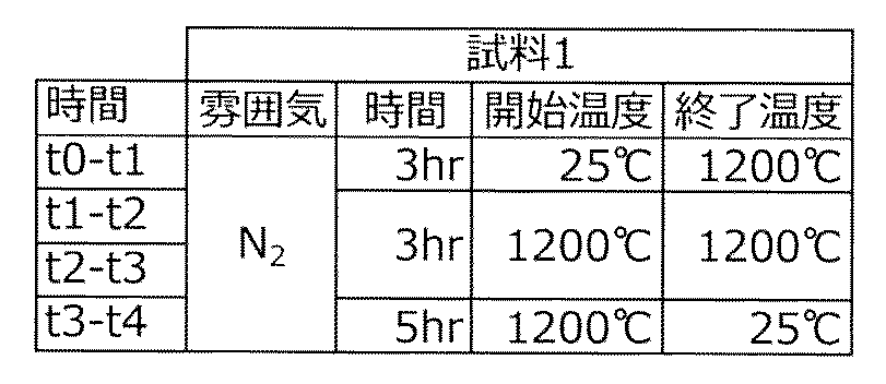
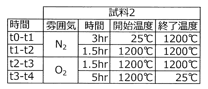
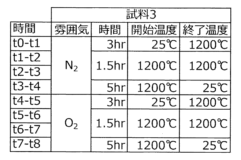
100a ターゲット
100b ターゲット
101 成膜室
103b マグネットユニット
110 バッキングプレート
110a バッキングプレート
110b バッキングプレート
120 ターゲットホルダ
120a ターゲットホルダ
120b ターゲットホルダ
122 ターゲットシールド
122a ターゲットシールド
122b ターゲットシールド
123 ターゲットシールド
130 マグネットユニット
130a マグネットユニット
130b マグネットユニット
130N マグネット
130N1 マグネット
130N2 マグネット
130S マグネット
132 マグネットホルダ
140 プラズマ
142 部材
160 基板
170 基板ホルダ
180a 磁力線
180b 磁力線
190 電源
191 電源
200 ペレット
200a ペレット
200b ペレット
200c ペレット
201 イオン
202 横成長部
206a 層
206b 層
206d ペレット
206e ペレット
206f ペレット
206m 層
210 バッキングプレート
220 基板
230 ターゲット
240 プラズマ
250 マグネット
260 加熱機構
400 基板
401 絶縁体
402 絶縁体
404 導電体
406a 半導体
406b 半導体
406c 半導体
408 絶縁体
409 絶縁体
412 絶縁体
413 導電体
416a 導電体
416b 導電体
422 絶縁体
428 絶縁体
450 半導体基板
452 絶縁体
454 導電体
456 領域
460 領域
462 絶縁体
464 絶縁体
466 絶縁体
468 絶縁体
472a 領域
472b 領域
474a 導電体
474b 導電体
474c 導電体
476a 導電体
476b 導電体
478a 導電体
478b 導電体
478c 導電体
480a 導電体
480b 導電体
480c 導電体
490 絶縁体
492 絶縁体
494 絶縁体
496a 導電体
496b 導電体
496c 導電体
496d 導電体
498a 導電体
498b 導電体
498c 導電体
498d 導電体
500 基板
502 絶縁体
503 絶縁体
504 導電体
506a 半導体
506b 半導体
506c 半導体
508 絶縁体
512 絶縁体
513 導電体
514 導電体
516a 導電体
516b 導電体
700 基板
704a 導電体
704b 導電体
706 半導体
706a 半導体
706b 半導体
712a 絶縁体
712b 絶縁体
714a 導電体
714b 導電体
716a 導電体
716b 導電体
718a 絶縁体
718b 絶縁体
718c 絶縁体
719 発光素子
720 絶縁体
721 絶縁体
731 端子
732 FPC
733a 配線
734 シール材
735 駆動回路
736 駆動回路
737 画素
741 トランジスタ
742 容量素子
743 スイッチ素子
744 信号線
750 基板
751 トランジスタ
752 容量素子
753 液晶素子
754 走査線
755 信号線
781 導電体
782 発光層
783 導電体
784 隔壁
791 導電体
792 絶縁体
793 液晶層
794 絶縁体
795 スペーサ
796 導電体
797 基板
801 半導体基板
802 基板
803 絶縁体
804 絶縁体
805 絶縁体
806 接着層
807 フィルタ
808 フィルタ
809 フィルタ
811 絶縁体
812 絶縁体
813 絶縁体
814 絶縁体
815 絶縁体
816 絶縁体
817 絶縁体
818 絶縁体
819 絶縁体
820 絶縁体
821 絶縁体
831 導電体
832 導電体
833 導電体
834 導電体
835 導電体
836 導電体
837 導電体
838 導電体
839 導電体
840 導電体
841 導電体
842 導電体
843 導電体
844 導電体
845 導電体
846 導電体
847 導電体
848 導電体
849 導電体
850 導電体
851 導電体
852 導電体
853 導電体
854 導電体
855 導電体
856 導電体
857 導電体
858 導電体
859 導電体
860 導電体
861 導電体
862 導電体
871 絶縁体
872 導電体
873 絶縁体
874 絶縁体
875 領域
876 領域
877 絶縁体
878 絶縁体
881 絶縁体
882 導電体
883 絶縁体
884 絶縁体
885 領域
886 領域
887 層
888 層
891 トランジスタ
892 トランジスタ
893 発光層
901 筐体
902 筐体
903 表示部
904 表示部
905 マイクロフォン
906 スピーカー
907 操作キー
908 スタイラス
911 筐体
912 筐体
913 表示部
914 表示部
915 接続部
916 操作キー
921 筐体
922 表示部
923 キーボード
924 ポインティングデバイス
931 筐体
932 冷蔵室用扉
933 冷凍室用扉
941 筐体
942 筐体
943 表示部
944 操作キー
945 レンズ
946 接続部
951 車体
952 車輪
953 ダッシュボード
954 ライト
1189 ROMインターフェース
1190 基板
1191 ALU
1192 ALUコントローラ
1193 インストラクションデコーダ
1194 インタラプトコントローラ
1195 タイミングコントローラ
1196 レジスタ
1197 レジスタコントローラ
1198 バスインターフェース
1199 ROM
1200 記憶素子
1201 回路
1202 回路
1203 スイッチ
1204 スイッチ
1206 論理素子
1207 容量素子
1208 容量素子
1209 トランジスタ
1210 トランジスタ
1213 トランジスタ
1214 トランジスタ
1220 回路
2000 撮像装置
2001 スイッチ
2002 スイッチ
2003 スイッチ
2010 画素部
2011 画素
2012 副画素
2012B 副画素
2012G 副画素
2012R 副画素
2020 光電変換素子
2030 画素回路
2031 配線
2047 配線
2048 配線
2049 配線
2050 配線
2053 配線
2054 フィルタ
2054B フィルタ
2054G フィルタ
2054R フィルタ
2055 レンズ
2056 光
2057 配線
2060 周辺回路
2070 周辺回路
2080 周辺回路
2090 周辺回路
2091 光源
2100 トランジスタ
2200 トランジスタ
2355 レンズ
2700 成膜装置
2300 シリコン基板
2310 層
2320 層
2328 絶縁体
2330 層
2340 層
2351 トランジスタ
2352 トランジスタ
2353 トランジスタ
2354 フィルタ
2360 フォトダイオード
2361 アノード
2363 低抵抗領域
2370 プラグ
2371 配線
2372 配線
2373 配線
2409 絶縁体
2422 絶縁体
2428 絶縁体
2701 大気側基板供給室
2702 大気側基板搬送室
2703a ロードロック室
2703b アンロードロック室
2704 搬送室
2705 基板加熱室
2706a 成膜室
2706b 成膜室
2706c 成膜室
2751 クライオトラップ
2752 基板受け渡しステージ
2761 カセットポート
2762 アライメントポート
2763 搬送ロボット
2764 ゲートバルブ
2765 加熱ステージ
2766a ターゲット
2766b ターゲット
2767 ターゲットシールド
2767a ターゲットシールド
2767b ターゲットシールド
2768 基板ホルダ
2769 基板
2770 真空ポンプ
2771 クライオポンプ
2772 ターボ分子ポンプ
2780 マスフローコントローラ
2781 精製機
2782 ガス加熱機構
2784 可変部材
2790a マグネットユニット
2790b マグネットユニット
2791 電源
3001 配線
3002 配線
3003 配線
3004 配線
3005 配線
3200 トランジスタ
3300 トランジスタ
3400 容量素子
5100 ペレット
5120 基板
5161 領域
Claims (9)
- インジウムと、亜鉛と、元素M(元素Mはアルミニウム、ガリウム、イットリウムまたはスズ)と、酸素と、を有する混合物を準備する第1のステップと、
前記混合物を、窒素を90体積%以上100体積%以下の濃度で有する第1の雰囲気で、第1の温度から第2の温度まで昇温する第2のステップと、
前記混合物を、酸素を10体積%以上100体積%以下の濃度で有する第2の雰囲気で、前記第2の温度から第3の温度まで降温する第3のステップと、を有することを特徴とするスパッタリング用ターゲットの作製方法。 - インジウムと、亜鉛と、元素M(元素Mはアルミニウム、ガリウム、イットリウムまたはスズ)と、酸素と、を有する混合物を準備する第1のステップと、
前記混合物を、窒素を90体積%以上100体積%以下の濃度で有する第1の雰囲気で、第1の温度から第2の温度まで昇温する第2のステップと、
前記混合物を、前記第1の雰囲気および前記第2の温度で、3分以上24時間未満保持する第3のステップと、
前記混合物を、酸素を10体積%以上100体積%以下の濃度で有する第2の雰囲気で、前記第2の温度から第3の温度まで降温する第4のステップと、を有することを特徴とするスパッタリング用ターゲットの作製方法。 - インジウムと、亜鉛と、元素M(元素Mはアルミニウム、ガリウム、イットリウムまたはスズ)と、酸素と、を有する混合物を凖備する第1のステップと、
前記混合物を、窒素を90体積%以上100体積%以下の濃度で有する第1の雰囲気で、第1の温度から第2の温度まで昇温する第2のステップと、
前記混合物を、前記第1の雰囲気および前記第2の温度で、3分以上24時間未満保持する第3のステップと、
前記混合物を、酸素を10体積%以上100体積%以下の濃度で有する第2の雰囲気および前記第2の温度で、3分以上24時間未満保持する第4のステップと、
前記混合物を、前記第2の雰囲気で、前記第2の温度から第3の温度まで降温する第4のステップと、を有することを特徴とするスパッタリング用ターゲットの作製方法。 - 請求項1乃至請求項3のいずれか一において、
前記第1の雰囲気は、露点−60℃未満のガスを有することを特徴とするスパッタリング用ターゲットの作製方法。 - 請求項1乃至請求項3のいずれか一において、
前記第2の雰囲気は、露点−60℃未満のガスを有することを特徴とするスパッタリング用ターゲットの作製方法。 - 請求項1乃至請求項3のいずれか一において、
前記第2の雰囲気は、乾燥空気を有することを特徴とするスパッタリング用ターゲットの作製方法。 - 請求項1乃至請求項3のいずれか一において、
前記第1の温度は、10℃以上300℃以下であることを特徴とするスパッタリング用ターゲットの作製方法。 - 請求項1乃至請求項3のいずれか一において、
前記第2の温度は、800℃以上1700℃以下であることを特徴とするスパッタリング用ターゲットの作製方法。 - 請求項1乃至請求項3のいずれか一において、
前記第3の温度は10℃以上300℃以下であることを特徴とするスパッタリング用ターゲットの作製方法。
Priority Applications (4)
| Application Number | Priority Date | Filing Date | Title |
|---|---|---|---|
| KR1020177018691A KR20170101233A (ko) | 2014-12-26 | 2014-12-16 | 스퍼터링용 타깃의 제작 방법 |
| US15/537,915 US10316404B2 (en) | 2014-12-26 | 2015-12-16 | Method for manufacturing sputtering target |
| CN201580070738.8A CN107109630A (zh) | 2014-12-26 | 2015-12-16 | 溅射靶材的制造方法 |
| JP2016565588A JP6608848B2 (ja) | 2014-12-26 | 2015-12-16 | スパッタリング用ターゲットの作製方法 |
Applications Claiming Priority (4)
| Application Number | Priority Date | Filing Date | Title |
|---|---|---|---|
| JP2014266201 | 2014-12-26 | ||
| JP2014-266201 | 2014-12-26 | ||
| JP2015004964 | 2015-01-14 | ||
| JP2015-004964 | 2015-01-14 |
Publications (1)
| Publication Number | Publication Date |
|---|---|
| WO2016103114A1 true WO2016103114A1 (ja) | 2016-06-30 |
Family
ID=56149350
Family Applications (1)
| Application Number | Title | Priority Date | Filing Date |
|---|---|---|---|
| PCT/IB2015/059650 Ceased WO2016103114A1 (ja) | 2014-12-26 | 2015-12-16 | スパッタリング用ターゲットの作製方法 |
Country Status (5)
| Country | Link |
|---|---|
| US (1) | US10316404B2 (ja) |
| JP (1) | JP6608848B2 (ja) |
| KR (1) | KR20170101233A (ja) |
| CN (1) | CN107109630A (ja) |
| WO (1) | WO2016103114A1 (ja) |
Families Citing this family (9)
| Publication number | Priority date | Publication date | Assignee | Title |
|---|---|---|---|---|
| CN114284364B (zh) * | 2016-02-12 | 2026-03-31 | 株式会社半导体能源研究所 | 半导体装置以及包括该半导体装置的显示装置 |
| KR102711637B1 (ko) | 2016-05-19 | 2024-09-27 | 가부시키가이샤 한도오따이 에네루기 켄큐쇼 | 복합 산화물 반도체 및 트랜지스터 |
| JP6569048B2 (ja) * | 2017-03-22 | 2019-09-04 | 国立研究開発法人日本原子力研究開発機構 | イオンビーム機能性透過膜、イオンビーム機能性透過膜を用いたビームライン機器、イオンビーム機能性透過膜を用いたフィルター機器、フィルター機器の調整方法 |
| US11148979B2 (en) * | 2017-10-31 | 2021-10-19 | James R. Glidewell Dental Ceramics, Inc. | Process for forming sintered ceramic bodies having improved properties |
| KR102341608B1 (ko) * | 2017-12-28 | 2021-12-22 | 엔지케이 인슐레이터 엘티디 | 압전성 재료 기판과 지지 기판의 접합체 및 그 제조 방법 |
| TWI820861B (zh) * | 2018-08-01 | 2023-11-01 | 日本商出光興產股份有限公司 | 結晶構造化合物、氧化物燒結體、濺鍍靶材、結晶質氧化物薄膜、非晶質氧化物薄膜、薄膜電晶體、及電子機器 |
| US10790466B2 (en) * | 2018-12-11 | 2020-09-29 | Feng-wen Yen | In-line system for mass production of organic optoelectronic device and manufacturing method using the same system |
| JP7515453B2 (ja) * | 2019-03-01 | 2024-07-12 | 株式会社半導体エネルギー研究所 | 半導体装置 |
| KR102701795B1 (ko) * | 2022-05-09 | 2024-09-02 | 한국전력공사 | 단결정 페로브스카이트의 제조 방법 및 이를 이용한 태양 전지의 제조 방법 |
Citations (3)
| Publication number | Priority date | Publication date | Assignee | Title |
|---|---|---|---|---|
| JP2012197219A (ja) * | 2011-03-07 | 2012-10-18 | Sumitomo Chemical Co Ltd | 酸化物焼結体、その製造方法およびそれを用いたターゲット |
| JP2013144841A (ja) * | 2011-06-08 | 2013-07-25 | Semiconductor Energy Lab Co Ltd | ターゲット、ターゲットの使用方法、及び半導体装置の作製方法 |
| JP2014051735A (ja) * | 2012-08-07 | 2014-03-20 | Semiconductor Energy Lab Co Ltd | スパッタリング用ターゲットの作製方法 |
Family Cites Families (110)
| Publication number | Priority date | Publication date | Assignee | Title |
|---|---|---|---|---|
| JPS60198861A (ja) | 1984-03-23 | 1985-10-08 | Fujitsu Ltd | 薄膜トランジスタ |
| JPH0244256B2 (ja) | 1987-01-28 | 1990-10-03 | Kagaku Gijutsucho Mukizaishitsu Kenkyushocho | Ingazn2o5deshimesarerurotsuhoshokeinosojokozoojusurukagobutsuoyobisonoseizoho |
| JPS63210023A (ja) | 1987-02-24 | 1988-08-31 | Natl Inst For Res In Inorg Mater | InGaZn↓4O↓7で示される六方晶系の層状構造を有する化合物およびその製造法 |
| JPH0244258B2 (ja) | 1987-02-24 | 1990-10-03 | Kagaku Gijutsucho Mukizaishitsu Kenkyushocho | Ingazn3o6deshimesarerurotsuhoshokeinosojokozoojusurukagobutsuoyobisonoseizoho |
| JPH0244260B2 (ja) | 1987-02-24 | 1990-10-03 | Kagaku Gijutsucho Mukizaishitsu Kenkyushocho | Ingazn5o8deshimesarerurotsuhoshokeinosojokozoojusurukagobutsuoyobisonoseizoho |
| JPH0244262B2 (ja) | 1987-02-27 | 1990-10-03 | Kagaku Gijutsucho Mukizaishitsu Kenkyushocho | Ingazn6o9deshimesarerurotsuhoshokeinosojokozoojusurukagobutsuoyobisonoseizoho |
| JPH0244263B2 (ja) | 1987-04-22 | 1990-10-03 | Kagaku Gijutsucho Mukizaishitsu Kenkyushocho | Ingazn7o10deshimesarerurotsuhoshokeinosojokozoojusurukagobutsuoyobisonoseizoho |
| JPH05251705A (ja) | 1992-03-04 | 1993-09-28 | Fuji Xerox Co Ltd | 薄膜トランジスタ |
| JP3479375B2 (ja) | 1995-03-27 | 2003-12-15 | 科学技術振興事業団 | 亜酸化銅等の金属酸化物半導体による薄膜トランジスタとpn接合を形成した金属酸化物半導体装置およびそれらの製造方法 |
| WO1997006554A2 (en) | 1995-08-03 | 1997-02-20 | Philips Electronics N.V. | Semiconductor device provided with transparent switching element |
| JP3625598B2 (ja) | 1995-12-30 | 2005-03-02 | 三星電子株式会社 | 液晶表示装置の製造方法 |
| JP4170454B2 (ja) | 1998-07-24 | 2008-10-22 | Hoya株式会社 | 透明導電性酸化物薄膜を有する物品及びその製造方法 |
| JP2000150861A (ja) | 1998-11-16 | 2000-05-30 | Tdk Corp | 酸化物薄膜 |
| JP3276930B2 (ja) | 1998-11-17 | 2002-04-22 | 科学技術振興事業団 | トランジスタ及び半導体装置 |
| TW460731B (en) | 1999-09-03 | 2001-10-21 | Ind Tech Res Inst | Electrode structure and production method of wide viewing angle LCD |
| JP4089858B2 (ja) | 2000-09-01 | 2008-05-28 | 国立大学法人東北大学 | 半導体デバイス |
| KR20020038482A (ko) | 2000-11-15 | 2002-05-23 | 모리시타 요이찌 | 박막 트랜지스터 어레이, 그 제조방법 및 그것을 이용한표시패널 |
| JP3997731B2 (ja) | 2001-03-19 | 2007-10-24 | 富士ゼロックス株式会社 | 基材上に結晶性半導体薄膜を形成する方法 |
| JP2002289859A (ja) | 2001-03-23 | 2002-10-04 | Minolta Co Ltd | 薄膜トランジスタ |
| JP3925839B2 (ja) | 2001-09-10 | 2007-06-06 | シャープ株式会社 | 半導体記憶装置およびその試験方法 |
| JP4090716B2 (ja) | 2001-09-10 | 2008-05-28 | 雅司 川崎 | 薄膜トランジスタおよびマトリクス表示装置 |
| JP4164562B2 (ja) | 2002-09-11 | 2008-10-15 | 独立行政法人科学技術振興機構 | ホモロガス薄膜を活性層として用いる透明薄膜電界効果型トランジスタ |
| EP1443130B1 (en) | 2001-11-05 | 2011-09-28 | Japan Science and Technology Agency | Natural superlattice homologous single crystal thin film, method for preparation thereof, and device using said single crystal thin film |
| JP4083486B2 (ja) | 2002-02-21 | 2008-04-30 | 独立行政法人科学技術振興機構 | LnCuO(S,Se,Te)単結晶薄膜の製造方法 |
| CN1445821A (zh) | 2002-03-15 | 2003-10-01 | 三洋电机株式会社 | ZnO膜和ZnO半导体层的形成方法、半导体元件及其制造方法 |
| JP3933591B2 (ja) | 2002-03-26 | 2007-06-20 | 淳二 城戸 | 有機エレクトロルミネッセント素子 |
| US7339187B2 (en) | 2002-05-21 | 2008-03-04 | State Of Oregon Acting By And Through The Oregon State Board Of Higher Education On Behalf Of Oregon State University | Transistor structures |
| JP2004022625A (ja) | 2002-06-13 | 2004-01-22 | Murata Mfg Co Ltd | 半導体デバイス及び該半導体デバイスの製造方法 |
| US7105868B2 (en) | 2002-06-24 | 2006-09-12 | Cermet, Inc. | High-electron mobility transistor with zinc oxide |
| US7067843B2 (en) | 2002-10-11 | 2006-06-27 | E. I. Du Pont De Nemours And Company | Transparent oxide semiconductor thin film transistors |
| JP4166105B2 (ja) | 2003-03-06 | 2008-10-15 | シャープ株式会社 | 半導体装置およびその製造方法 |
| JP2004273732A (ja) | 2003-03-07 | 2004-09-30 | Sharp Corp | アクティブマトリクス基板およびその製造方法 |
| JP4108633B2 (ja) | 2003-06-20 | 2008-06-25 | シャープ株式会社 | 薄膜トランジスタおよびその製造方法ならびに電子デバイス |
| US7262463B2 (en) | 2003-07-25 | 2007-08-28 | Hewlett-Packard Development Company, L.P. | Transistor including a deposited channel region having a doped portion |
| EP2413366B1 (en) | 2004-03-12 | 2017-01-11 | Japan Science And Technology Agency | A switching element of LCDs or organic EL displays |
| US7145174B2 (en) | 2004-03-12 | 2006-12-05 | Hewlett-Packard Development Company, Lp. | Semiconductor device |
| US7297977B2 (en) | 2004-03-12 | 2007-11-20 | Hewlett-Packard Development Company, L.P. | Semiconductor device |
| US7282782B2 (en) | 2004-03-12 | 2007-10-16 | Hewlett-Packard Development Company, L.P. | Combined binary oxide semiconductor device |
| US7211825B2 (en) | 2004-06-14 | 2007-05-01 | Yi-Chi Shih | Indium oxide-based thin film transistors and circuits |
| JP2006100760A (ja) | 2004-09-02 | 2006-04-13 | Casio Comput Co Ltd | 薄膜トランジスタおよびその製造方法 |
| US7285501B2 (en) | 2004-09-17 | 2007-10-23 | Hewlett-Packard Development Company, L.P. | Method of forming a solution processed device |
| US7298084B2 (en) | 2004-11-02 | 2007-11-20 | 3M Innovative Properties Company | Methods and displays utilizing integrated zinc oxide row and column drivers in conjunction with organic light emitting diodes |
| US7863611B2 (en) | 2004-11-10 | 2011-01-04 | Canon Kabushiki Kaisha | Integrated circuits utilizing amorphous oxides |
| RU2369940C2 (ru) | 2004-11-10 | 2009-10-10 | Кэнон Кабусики Кайся | Аморфный оксид и полевой транзистор с его использованием |
| US7453065B2 (en) | 2004-11-10 | 2008-11-18 | Canon Kabushiki Kaisha | Sensor and image pickup device |
| US7829444B2 (en) | 2004-11-10 | 2010-11-09 | Canon Kabushiki Kaisha | Field effect transistor manufacturing method |
| CA2585063C (en) | 2004-11-10 | 2013-01-15 | Canon Kabushiki Kaisha | Light-emitting device |
| EP1815530B1 (en) | 2004-11-10 | 2021-02-17 | Canon Kabushiki Kaisha | Field effect transistor employing an amorphous oxide |
| US7791072B2 (en) | 2004-11-10 | 2010-09-07 | Canon Kabushiki Kaisha | Display |
| US7579224B2 (en) | 2005-01-21 | 2009-08-25 | Semiconductor Energy Laboratory Co., Ltd. | Method for manufacturing a thin film semiconductor device |
| TWI505473B (zh) | 2005-01-28 | 2015-10-21 | 半導體能源研究所股份有限公司 | 半導體裝置,電子裝置,和半導體裝置的製造方法 |
| TWI390735B (zh) | 2005-01-28 | 2013-03-21 | 半導體能源研究所股份有限公司 | 半導體裝置,電子裝置,和半導體裝置的製造方法 |
| US7858451B2 (en) | 2005-02-03 | 2010-12-28 | Semiconductor Energy Laboratory Co., Ltd. | Electronic device, semiconductor device and manufacturing method thereof |
| US7948171B2 (en) | 2005-02-18 | 2011-05-24 | Semiconductor Energy Laboratory Co., Ltd. | Light emitting device |
| US20060197092A1 (en) | 2005-03-03 | 2006-09-07 | Randy Hoffman | System and method for forming conductive material on a substrate |
| US8681077B2 (en) | 2005-03-18 | 2014-03-25 | Semiconductor Energy Laboratory Co., Ltd. | Semiconductor device, and display device, driving method and electronic apparatus thereof |
| WO2006105077A2 (en) | 2005-03-28 | 2006-10-05 | Massachusetts Institute Of Technology | Low voltage thin film transistor with high-k dielectric material |
| US7645478B2 (en) | 2005-03-31 | 2010-01-12 | 3M Innovative Properties Company | Methods of making displays |
| US8300031B2 (en) | 2005-04-20 | 2012-10-30 | Semiconductor Energy Laboratory Co., Ltd. | Semiconductor device comprising transistor having gate and drain connected through a current-voltage conversion element |
| JP2006344849A (ja) | 2005-06-10 | 2006-12-21 | Casio Comput Co Ltd | 薄膜トランジスタ |
| US7691666B2 (en) | 2005-06-16 | 2010-04-06 | Eastman Kodak Company | Methods of making thin film transistors comprising zinc-oxide-based semiconductor materials and transistors made thereby |
| US7402506B2 (en) | 2005-06-16 | 2008-07-22 | Eastman Kodak Company | Methods of making thin film transistors comprising zinc-oxide-based semiconductor materials and transistors made thereby |
| US7507618B2 (en) | 2005-06-27 | 2009-03-24 | 3M Innovative Properties Company | Method for making electronic devices using metal oxide nanoparticles |
| KR100711890B1 (ko) | 2005-07-28 | 2007-04-25 | 삼성에스디아이 주식회사 | 유기 발광표시장치 및 그의 제조방법 |
| JP2007059128A (ja) | 2005-08-23 | 2007-03-08 | Canon Inc | 有機el表示装置およびその製造方法 |
| JP2007073705A (ja) | 2005-09-06 | 2007-03-22 | Canon Inc | 酸化物半導体チャネル薄膜トランジスタおよびその製造方法 |
| JP5116225B2 (ja) | 2005-09-06 | 2013-01-09 | キヤノン株式会社 | 酸化物半導体デバイスの製造方法 |
| JP4280736B2 (ja) | 2005-09-06 | 2009-06-17 | キヤノン株式会社 | 半導体素子 |
| JP4850457B2 (ja) | 2005-09-06 | 2012-01-11 | キヤノン株式会社 | 薄膜トランジスタ及び薄膜ダイオード |
| EP3614442A3 (en) | 2005-09-29 | 2020-03-25 | Semiconductor Energy Laboratory Co., Ltd. | Semiconductor device having oxide semiconductor layer and manufactoring method thereof |
| JP5037808B2 (ja) | 2005-10-20 | 2012-10-03 | キヤノン株式会社 | アモルファス酸化物を用いた電界効果型トランジスタ、及び該トランジスタを用いた表示装置 |
| CN101283444B (zh) | 2005-11-15 | 2011-01-26 | 株式会社半导体能源研究所 | 半导体器件及其制造方法 |
| TWI292281B (en) | 2005-12-29 | 2008-01-01 | Ind Tech Res Inst | Pixel structure of active organic light emitting diode and method of fabricating the same |
| US7867636B2 (en) | 2006-01-11 | 2011-01-11 | Murata Manufacturing Co., Ltd. | Transparent conductive film and method for manufacturing the same |
| JP4977478B2 (ja) | 2006-01-21 | 2012-07-18 | 三星電子株式会社 | ZnOフィルム及びこれを用いたTFTの製造方法 |
| US7576394B2 (en) | 2006-02-02 | 2009-08-18 | Kochi Industrial Promotion Center | Thin film transistor including low resistance conductive thin films and manufacturing method thereof |
| US7977169B2 (en) | 2006-02-15 | 2011-07-12 | Kochi Industrial Promotion Center | Semiconductor device including active layer made of zinc oxide with controlled orientations and manufacturing method thereof |
| KR20070101595A (ko) | 2006-04-11 | 2007-10-17 | 삼성전자주식회사 | ZnO TFT |
| US20070252928A1 (en) | 2006-04-28 | 2007-11-01 | Toppan Printing Co., Ltd. | Structure, transmission type liquid crystal display, reflection type display and manufacturing method thereof |
| JP5028033B2 (ja) | 2006-06-13 | 2012-09-19 | キヤノン株式会社 | 酸化物半導体膜のドライエッチング方法 |
| JP4609797B2 (ja) | 2006-08-09 | 2011-01-12 | Nec液晶テクノロジー株式会社 | 薄膜デバイス及びその製造方法 |
| JP4999400B2 (ja) | 2006-08-09 | 2012-08-15 | キヤノン株式会社 | 酸化物半導体膜のドライエッチング方法 |
| JP5358891B2 (ja) * | 2006-08-11 | 2013-12-04 | 日立金属株式会社 | 酸化亜鉛焼結体の製造方法 |
| JP4332545B2 (ja) | 2006-09-15 | 2009-09-16 | キヤノン株式会社 | 電界効果型トランジスタ及びその製造方法 |
| JP4274219B2 (ja) | 2006-09-27 | 2009-06-03 | セイコーエプソン株式会社 | 電子デバイス、有機エレクトロルミネッセンス装置、有機薄膜半導体装置 |
| JP5164357B2 (ja) | 2006-09-27 | 2013-03-21 | キヤノン株式会社 | 半導体装置及び半導体装置の製造方法 |
| US7622371B2 (en) | 2006-10-10 | 2009-11-24 | Hewlett-Packard Development Company, L.P. | Fused nanocrystal thin film semiconductor and method |
| US7772021B2 (en) | 2006-11-29 | 2010-08-10 | Samsung Electronics Co., Ltd. | Flat panel displays comprising a thin-film transistor having a semiconductive oxide in its channel and methods of fabricating the same for use in flat panel displays |
| JP2008140684A (ja) | 2006-12-04 | 2008-06-19 | Toppan Printing Co Ltd | カラーelディスプレイおよびその製造方法 |
| KR101303578B1 (ko) | 2007-01-05 | 2013-09-09 | 삼성전자주식회사 | 박막 식각 방법 |
| US8207063B2 (en) | 2007-01-26 | 2012-06-26 | Eastman Kodak Company | Process for atomic layer deposition |
| KR100851215B1 (ko) | 2007-03-14 | 2008-08-07 | 삼성에스디아이 주식회사 | 박막 트랜지스터 및 이를 이용한 유기 전계 발광표시장치 |
| US7795613B2 (en) | 2007-04-17 | 2010-09-14 | Toppan Printing Co., Ltd. | Structure with transistor |
| KR101325053B1 (ko) | 2007-04-18 | 2013-11-05 | 삼성디스플레이 주식회사 | 박막 트랜지스터 기판 및 이의 제조 방법 |
| KR20080094300A (ko) | 2007-04-19 | 2008-10-23 | 삼성전자주식회사 | 박막 트랜지스터 및 그 제조 방법과 박막 트랜지스터를포함하는 평판 디스플레이 |
| KR101334181B1 (ko) | 2007-04-20 | 2013-11-28 | 삼성전자주식회사 | 선택적으로 결정화된 채널층을 갖는 박막 트랜지스터 및 그제조 방법 |
| WO2008133345A1 (en) | 2007-04-25 | 2008-11-06 | Canon Kabushiki Kaisha | Oxynitride semiconductor |
| KR101345376B1 (ko) | 2007-05-29 | 2013-12-24 | 삼성전자주식회사 | ZnO 계 박막 트랜지스터 및 그 제조방법 |
| US8202365B2 (en) | 2007-12-17 | 2012-06-19 | Fujifilm Corporation | Process for producing oriented inorganic crystalline film, and semiconductor device using the oriented inorganic crystalline film |
| JP4623179B2 (ja) | 2008-09-18 | 2011-02-02 | ソニー株式会社 | 薄膜トランジスタおよびその製造方法 |
| JP5451280B2 (ja) | 2008-10-09 | 2014-03-26 | キヤノン株式会社 | ウルツ鉱型結晶成長用基板およびその製造方法ならびに半導体装置 |
| WO2010088629A1 (en) * | 2009-02-02 | 2010-08-05 | The Regents Of The University Of California | Reversible ethylene oxide capture in porous frameworks |
| WO2011058882A1 (en) | 2009-11-13 | 2011-05-19 | Semiconductor Energy Laboratory Co., Ltd. | Sputtering target and manufacturing method thereof, and transistor |
| KR20120106950A (ko) | 2009-11-13 | 2012-09-27 | 가부시키가이샤 한도오따이 에네루기 켄큐쇼 | 스퍼터링 타겟 및 그 제작 방법 및 트랜지스터 |
| WO2011062043A1 (en) * | 2009-11-20 | 2011-05-26 | Semiconductor Energy Laboratory Co., Ltd. | Method for manufacturing semiconductor device |
| WO2011115029A1 (ja) * | 2010-03-16 | 2011-09-22 | 日本曹達株式会社 | 植物病害防除剤 |
| DE102010047756B3 (de) * | 2010-10-08 | 2012-03-01 | Heraeus Materials Technology Gmbh & Co. Kg | Sputtertarget mit amorphen und mikrokristallinen Anteilen sowie Verfahren zur Herstellung eines Sputtertargets |
| JP6016532B2 (ja) * | 2011-09-07 | 2016-10-26 | 株式会社半導体エネルギー研究所 | 半導体装置 |
| KR20150023054A (ko) | 2012-06-29 | 2015-03-04 | 가부시키가이샤 한도오따이 에네루기 켄큐쇼 | 스퍼터링용 타겟의 사용 방법 및 산화물막의 제작 방법 |
| US10557192B2 (en) | 2012-08-07 | 2020-02-11 | Semiconductor Energy Laboratory Co., Ltd. | Method for using sputtering target and method for forming oxide film |
-
2014
- 2014-12-16 KR KR1020177018691A patent/KR20170101233A/ko not_active Withdrawn
-
2015
- 2015-12-16 WO PCT/IB2015/059650 patent/WO2016103114A1/ja not_active Ceased
- 2015-12-16 JP JP2016565588A patent/JP6608848B2/ja active Active
- 2015-12-16 CN CN201580070738.8A patent/CN107109630A/zh active Pending
- 2015-12-16 US US15/537,915 patent/US10316404B2/en active Active
Patent Citations (3)
| Publication number | Priority date | Publication date | Assignee | Title |
|---|---|---|---|---|
| JP2012197219A (ja) * | 2011-03-07 | 2012-10-18 | Sumitomo Chemical Co Ltd | 酸化物焼結体、その製造方法およびそれを用いたターゲット |
| JP2013144841A (ja) * | 2011-06-08 | 2013-07-25 | Semiconductor Energy Lab Co Ltd | ターゲット、ターゲットの使用方法、及び半導体装置の作製方法 |
| JP2014051735A (ja) * | 2012-08-07 | 2014-03-20 | Semiconductor Energy Lab Co Ltd | スパッタリング用ターゲットの作製方法 |
Also Published As
| Publication number | Publication date |
|---|---|
| CN107109630A (zh) | 2017-08-29 |
| JPWO2016103114A1 (ja) | 2017-12-21 |
| JP6608848B2 (ja) | 2019-11-20 |
| KR20170101233A (ko) | 2017-09-05 |
| US20170350002A1 (en) | 2017-12-07 |
| US10316404B2 (en) | 2019-06-11 |
Similar Documents
| Publication | Publication Date | Title |
|---|---|---|
| JP6608848B2 (ja) | スパッタリング用ターゲットの作製方法 | |
| JP6637822B2 (ja) | 半導体装置 | |
| JP6580452B2 (ja) | 酸化物の作製方法 | |
| JP2024028810A (ja) | 半導体装置 | |
| JP6714372B2 (ja) | 酸化膜の成膜方法 | |
| JP2016180178A (ja) | 酸化物およびその作製方法 | |
| JP2016164308A (ja) | 酸化物の作製方法およびスパッタリング装置 | |
| TW201633410A (zh) | 半導體裝置、顯示裝置、顯示模組、電子裝置、氧化物以及氧化物的製造 方法 | |
| JP6681151B2 (ja) | 酸化物半導体膜の作製方法 | |
| JP2015109427A (ja) | 酸化物半導体膜の作製方法 | |
| JP6705810B2 (ja) | 半導体装置 | |
| JP2015201640A (ja) | 半導体装置、モジュールおよび電子機器 |
Legal Events
| Date | Code | Title | Description |
|---|---|---|---|
| 121 | Ep: the epo has been informed by wipo that ep was designated in this application |
Ref document number: 15872061 Country of ref document: EP Kind code of ref document: A1 |
|
| ENP | Entry into the national phase |
Ref document number: 2016565588 Country of ref document: JP Kind code of ref document: A |
|
| WWE | Wipo information: entry into national phase |
Ref document number: 15537915 Country of ref document: US |
|
| NENP | Non-entry into the national phase |
Ref country code: DE |
|
| ENP | Entry into the national phase |
Ref document number: 20177018691 Country of ref document: KR Kind code of ref document: A |
|
| 122 | Ep: pct application non-entry in european phase |
Ref document number: 15872061 Country of ref document: EP Kind code of ref document: A1 |