WO2016080262A1 - 静電チャック装置 - Google Patents
静電チャック装置 Download PDFInfo
- Publication number
- WO2016080262A1 WO2016080262A1 PCT/JP2015/081732 JP2015081732W WO2016080262A1 WO 2016080262 A1 WO2016080262 A1 WO 2016080262A1 JP 2015081732 W JP2015081732 W JP 2015081732W WO 2016080262 A1 WO2016080262 A1 WO 2016080262A1
- Authority
- WO
- WIPO (PCT)
- Prior art keywords
- ceramic plate
- adhesive layer
- chuck device
- electrostatic chuck
- heating member
- Prior art date
- Legal status (The legal status is an assumption and is not a legal conclusion. Google has not performed a legal analysis and makes no representation as to the accuracy of the status listed.)
- Ceased
Links
Images



Classifications
-
- H—ELECTRICITY
- H10—SEMICONDUCTOR DEVICES; ELECTRIC SOLID-STATE DEVICES NOT OTHERWISE PROVIDED FOR
- H10P—GENERIC PROCESSES OR APPARATUS FOR THE MANUFACTURE OR TREATMENT OF DEVICES COVERED BY CLASS H10
- H10P72/00—Handling or holding of wafers, substrates or devices during manufacture or treatment thereof
- H10P72/70—Handling or holding of wafers, substrates or devices during manufacture or treatment thereof for supporting or gripping
- H10P72/72—Handling or holding of wafers, substrates or devices during manufacture or treatment thereof for supporting or gripping using electrostatic chucks
- H10P72/722—Details of electrostatic chucks
-
- H—ELECTRICITY
- H10—SEMICONDUCTOR DEVICES; ELECTRIC SOLID-STATE DEVICES NOT OTHERWISE PROVIDED FOR
- H10P—GENERIC PROCESSES OR APPARATUS FOR THE MANUFACTURE OR TREATMENT OF DEVICES COVERED BY CLASS H10
- H10P72/00—Handling or holding of wafers, substrates or devices during manufacture or treatment thereof
- H10P72/04—Apparatus for manufacture or treatment
- H10P72/0431—Apparatus for thermal treatment
- H10P72/0434—Apparatus for thermal treatment mainly by convection
-
- H—ELECTRICITY
- H10—SEMICONDUCTOR DEVICES; ELECTRIC SOLID-STATE DEVICES NOT OTHERWISE PROVIDED FOR
- H10P—GENERIC PROCESSES OR APPARATUS FOR THE MANUFACTURE OR TREATMENT OF DEVICES COVERED BY CLASS H10
- H10P72/00—Handling or holding of wafers, substrates or devices during manufacture or treatment thereof
- H10P72/04—Apparatus for manufacture or treatment
- H10P72/0431—Apparatus for thermal treatment
- H10P72/0432—Apparatus for thermal treatment mainly by conduction
-
- H—ELECTRICITY
- H10—SEMICONDUCTOR DEVICES; ELECTRIC SOLID-STATE DEVICES NOT OTHERWISE PROVIDED FOR
- H10P—GENERIC PROCESSES OR APPARATUS FOR THE MANUFACTURE OR TREATMENT OF DEVICES COVERED BY CLASS H10
- H10P72/00—Handling or holding of wafers, substrates or devices during manufacture or treatment thereof
- H10P72/06—Apparatus for monitoring, sorting, marking, testing or measuring
- H10P72/0602—Temperature monitoring
-
- H—ELECTRICITY
- H10—SEMICONDUCTOR DEVICES; ELECTRIC SOLID-STATE DEVICES NOT OTHERWISE PROVIDED FOR
- H10P—GENERIC PROCESSES OR APPARATUS FOR THE MANUFACTURE OR TREATMENT OF DEVICES COVERED BY CLASS H10
- H10P72/00—Handling or holding of wafers, substrates or devices during manufacture or treatment thereof
- H10P72/70—Handling or holding of wafers, substrates or devices during manufacture or treatment thereof for supporting or gripping
- H10P72/72—Handling or holding of wafers, substrates or devices during manufacture or treatment thereof for supporting or gripping using electrostatic chucks
-
- B—PERFORMING OPERATIONS; TRANSPORTING
- B23—MACHINE TOOLS; METAL-WORKING NOT OTHERWISE PROVIDED FOR
- B23Q—DETAILS, COMPONENTS, OR ACCESSORIES FOR MACHINE TOOLS, e.g. ARRANGEMENTS FOR COPYING OR CONTROLLING; MACHINE TOOLS IN GENERAL CHARACTERISED BY THE CONSTRUCTION OF PARTICULAR DETAILS OR COMPONENTS; COMBINATIONS OR ASSOCIATIONS OF METAL-WORKING MACHINES, NOT DIRECTED TO A PARTICULAR RESULT
- B23Q3/00—Devices holding, supporting, or positioning work or tools, of a kind normally removable from the machine
- B23Q3/15—Devices for holding work using magnetic or electric force acting directly on the work
Definitions
- the present invention relates to an electrostatic chuck device.
- This application claims priority based on Japanese Patent Application No. 2014-235455 for which it applied to Japan on November 20, 2014, and uses the content here.
- an electrostatic chuck apparatus is used as an apparatus for simply mounting and fixing a wafer on a sample stage and maintaining the wafer at a desired temperature. Is used.
- the electrostatic chuck device is formed by bonding and integrating a ceramic base in which a plate electrode for electrostatic adsorption is embedded inside and a base portion in which a refrigerant flow path for refrigerant circulation is formed in an adhesive layer.
- Patent Document 1 a use temperature of 200 ° C. or lower (for example, Patent Document 2 and Patent Document 3).
- Patent Document 3 describes a silicone-based resin composition as an adhesive layer that can be used in a temperature range of 200 ° C. or lower.
- JP 2013-247342 A Japanese Patent Laying-Open No. 2005-200221 JP-A-4-287344
- the adhesive layer having heat resistance up to a high temperature region has a problem that it lacks flexibility.
- the base part, the ceramic base, and the adhesive layer that bonds them expand or contract due to heating by the heating member and plasma, the cooling function of the base part, etc. Stress is generated. Due to these stresses, the ceramic base cannot be sufficiently fixed to the base portion, resulting in misalignment or the like.
- an adhesive layer that does not have heat resistance in a flexible high temperature region does not have sufficient heat resistance, and thus dissolves or decomposes in a high temperature environment such as 200 ° C. or higher. For this reason, even when an adhesive layer having insufficient heat resistance is used, the ceramic base cannot be sufficiently fixed to the base portion, resulting in misalignment or the like.
- heat resistance of the adhesive layer means that the adhesive layer does not dissolve or decompose with respect to applied heat and can maintain a certain state.
- the adhesive layer has a heat resistance of 200 ° C. or higher means that the adhesive layer does not dissolve or decompose even when the adhesive layer reaches a temperature of 200 ° C.
- the present invention has been made in view of the above problems, and an object thereof is to provide an electrostatic chuck device having high heat resistance that can be used even in a high temperature environment.
- An electrostatic chuck device has a first surface on which a plate-like sample can be placed and a second surface opposite to the first surface, and includes a first electrode having an electrostatic chuck.
- the first adhesive layer has higher heat resistance than the second adhesive layer, and the Young's modulus of the second adhesive layer is smaller than the Young's modulus of the first adhesive layer.
- the bonding interface between the first ceramic plate and the second ceramic plate that is closest to the heating member and has a high temperature is bonded by the first bonding layer having high heat resistance. For this reason, it is possible to suppress the deterioration of the first adhesive layer even under a high temperature environment. That is, there is no problem that the in-plane temperature uniformity is lowered. Moreover, since the first ceramic plate and the second ceramic plate are ceramics, there is no significant difference in their respective thermal expansion coefficients. Therefore, even if the first ceramic plate and the second ceramic plate are bonded via the first adhesive layer lacking in flexibility, they do not peel from each other.
- the bonding interface between the second ceramic plate and the cooling base portion that is far from the heating member and close to the cooling base portion is bonded by a flexible second bonding layer. Since the heat generated in the heating member is transmitted to the second adhesive layer via the first adhesive layer and the second ceramic plate, the temperature is sufficiently lowered when the heat is transmitted to the second adhesive layer. As a result, even when the second adhesive layer having lower heat resistance than the first adhesive layer is used, it is possible to suppress the deterioration of the second adhesive without being dissolved or decomposed.
- the Young's modulus of the second adhesive layer is smaller than the Young's modulus of the first adhesive layer.
- the heat transfer coefficient of the first and second adhesive layers may be 1/2 or less of the heat transfer coefficient of the second ceramic plate.
- anisotropy can be imparted to the heat transfer properties in the in-plane direction and the vertical direction parallel to the mounting surface of the electrostatic chuck device.
- the electrostatic chuck device is required to be soaking in the in-plane direction in order to improve the soaking property of the plate-like sample to be placed.
- the vertical direction it is required to satisfy both the desire to efficiently exhaust the heat generated by the heating member and the desire to prevent the temperature of the conflicting second adhesive layer from becoming too high. It is done.
- the heat transfer coefficient of the first and second adhesive layers is low, the generated heat is difficult to transfer between the first and second adhesive layers and the second ceramic plate. That is, the temperature of the second adhesive layer can be suppressed from becoming high.
- the heat transfer coefficient of the second ceramic plate is high, it is possible to improve the heat uniformity due to the heat transfer in the in-plane direction and the heat exhaustion of the generated heat.
- the cooling base portion may have a first recess, and at least the first adhesive layer and the second ceramic plate may be fitted.
- the first ceramic plate has a bank portion surrounding the second surface, and the first recess is formed by the bank portion and the second surface.
- the second ceramic plate may be fitted through the adhesive layer.
- the heating member and the first adhesive layer can be prevented from coming into direct contact with the cooling base portion.
- the thermal uniformity can be improved.
- production of position shift etc. can be suppressed by fitting a 1st ceramic plate and a 2nd ceramic plate with 2 steps
- the exposure of the first adhesive layer and the second adhesive layer to the surface irradiated with plasma in a process such as etching is reduced, and the first adhesive layer and the second adhesive layer are deteriorated due to deterioration or the like. Consumption can be suppressed.
- a plurality of auxiliary heating members are fixed to the surface of the second ceramic plate on the first ceramic plate side, and the auxiliary heating members can be individually temperature controlled. Also good.
- the heat unevenness generated in the heating member can be compensated for by the auxiliary heating member. That is, the thermal uniformity of the electrostatic chuck device can be improved.
- the electrostatic chuck device may be composed of a plurality of members from which the heating member is separated, and each may be individually driven. Further, the second ceramic plate may be divided in a heat transfer manner in accordance with a region where the temperature of the separated heating member can be individually controlled.
- the temperature of the separated heating member can be controlled for each region, and the thermal uniformity of the electrostatic chuck device can be improved.
- the second ceramic plate is thermally divided in accordance with this region, heat conduction in the in-plane direction is suppressed through the second ceramic plate, and temperature controllability for each region is achieved. Can be increased.
- heat conduction in the in-plane direction is allowed in the concentric direction (circumferential direction), but the heat conduction in the radial direction can be a factor in inhibiting thermal uniformity, so the regions are concentrically divided. It is preferable to do.
- a third adhesive layer having higher heat resistance than the second adhesive layer may be interposed between the second ceramic plate and the second adhesive layer.
- One or more ceramic plates may be interposed between the second ceramic plate and the second adhesive layer.
- the second adhesive layer can be prevented from reaching a high temperature. If the temperature of the second adhesive layer is not increased, the heat resistance of the second adhesive layer can be maintained, and occurrence of misalignment or the like and deterioration of the second adhesive layer can be suppressed. Further, since the third adhesive layer is considered to have a higher temperature than the second adhesive layer, it is preferable that the third adhesive layer has higher heat resistance than the second adhesive layer. Further, when one or more ceramic plates are interposed, each ceramic plate is preferably bonded via a third adhesive layer or the like having higher heat resistance than the second adhesive layer.
- the electrostatic chuck device of the present invention it is possible to provide an electrostatic chuck device with improved heat resistance that can be used even at a high temperature of 200 ° C. or higher.
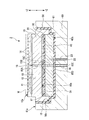
- FIG. 1 is a cross-sectional view schematically showing the electrostatic chuck device 1 of the first embodiment.
- the electrostatic chuck device 1 according to the first embodiment has a first surface 10a on which a plate-like sample W can be placed and a second surface 10b opposite to the first surface 10a.
- the first ceramic plate 10, the heating member 20 fixed to the second surface 10 b, and the second ceramic plate 10 and the heating member 20 bonded to the first ceramic plate 10 and the heating member 20 via the first adhesive layer 30.
- Ceramic plate 40, and a cooling base portion 60 bonded to the second ceramic plate 40 via a second adhesive layer 50. That is, the cooling base 60, the second adhesive layer 50, the second ceramic plate 40, the first adhesive layer 30, the heating member 20, and the first ceramic plate 10 are laminated in this order in the + Z direction of FIG. It has a structure.
- the first ceramic plate 10 includes a mounting plate 11 on which a plate-like sample W such as a semiconductor wafer, a metal wafer, or a glass substrate is mounted, a support plate 12 that is disposed to face the mounting plate 11, and a mounting plate 11. An internal electrode 13 for electrostatic attraction is sandwiched between the plate 11 and the support plate 12.
- the first ceramic plate 10 has a first surface 10a on which the plate-like sample W is placed and a second surface 10b on the opposite side.
- the mounting plate 11 and the support plate 12 have a disk shape with the same shape of the stacked surfaces, and are an aluminum oxide-silicon carbide (Al 2 O 3 —SiC) composite sintered body, aluminum oxide (Al 2 Insulating ceramics having mechanical strength, corrosive gas and durability against plasma, such as O 3 ) sintered body, aluminum nitride (AlN) sintered body, yttrium oxide (Y 2 O 3 ) sintered body It is preferable to consist of a sintered body.
- Al 2 O 3 —SiC aluminum oxide-silicon carbide
- AlN aluminum nitride
- Y 2 O 3 yttrium oxide
- a plurality of protrusions 14 may be provided on the first surface 10 a of the mounting plate 11. By causing the gas to flow between the protrusions 14, the in-plane temperature uniformity of the plate-like sample W placed by the gas flow can be improved.
- the protrusion 14 has a generally truncated cone shape, but is not limited to this shape.
- the cross section may be rectangular or triangular.
- the support plate 12 is provided with a hole penetrating in the thickness direction. The internal electrode terminal 15 is inserted through this hole.
- the internal electrode 13 for electrostatic adsorption is used as an electrode for an electrostatic chuck for generating a charge and fixing the plate-like sample W with an electrostatic adsorption force. Adjust as appropriate.
- the material of the electrostatic adsorption internal electrode 13 is selected in consideration of the difference in thermal expansion from the materials used for the mounting plate 11 and the support plate 12, heat resistance, and the like.
- the internal electrode 13 for electrostatic adsorption includes an aluminum oxide-tantalum carbide (Al 2 O 3 —Ta 4 C 5 ) conductive composite sintered body, an aluminum oxide-tungsten (Al 2 O 3 —W) conductive composite fired body.
- AlN-W Aluminum nitride-tungsten
- AlN-Ta Aluminum nitride-tantalum
- Conductive ceramics such as composite sintered bodies, yttrium oxide-molybdenum (Y 2 O 3 -Mo) conductive composite sintered bodies, or refractory metals such as tungsten (W), tantalum (Ta
- the thickness of the internal electrode 13 for electrostatic adsorption is not particularly limited, but is preferably 0.1 ⁇ m or more and 100 ⁇ m or less, and more preferably 5 ⁇ m or more and 20 ⁇ m or less. If the thickness is less than 0.1 ⁇ m, sufficient conductivity cannot be ensured. On the other hand, if the thickness exceeds 100 ⁇ m, the electrostatic chucking internal electrode 13, the mounting plate 11, and the support plate 12 are not connected. This is because cracks are likely to occur at the bonding interface between the electrostatic adsorption internal electrode 13 and the mounting plate 11 and the support plate 12 due to the difference in thermal expansion coefficient.
- the electrostatic adsorption internal electrode 13 having such a thickness can be easily formed by a film forming method such as a sputtering method or a vapor deposition method, or a coating method such as a screen printing method.
- the internal electrode terminal 15 is provided to apply a DC voltage to the electrostatic adsorption internal electrode 13.
- the internal electrode terminal 15 includes a lead electrode 15A, a first conductive adhesive 15B, a first lead electrode 15C, a second conductive adhesive 15D, and a second lead electrode 15E.
- the internal electrode terminal 15 extends from the electrostatic adsorption internal electrode 13 through the hole in the thickness direction, and is exposed on the surface of the cooling base 60 opposite to the surface on the first ceramic plate 10 side.
- the internal electrode terminal 15 is insulated by at least the insulator 16 with respect to the cooling base portion 60.
- the material of the extraction electrode 15A, the first extraction electrode 15C, and the second extraction electrode 15E among the internal electrode terminals 15 is not particularly limited as long as it is a conductive material having excellent heat resistance, but the coefficient of thermal expansion is static. What approximates the thermal expansion coefficient of the internal electrode 13 for electroadsorption, the support plate 12, and the 2nd ceramic plate mentioned later is preferable.
- a conductive ceramic constituting the internal electrode 13 for electrostatic attraction, or a metal material such as tungsten (W), tantalum (Ta), molybdenum (Mo), niobium (Nb), or Kovar alloy is preferably used. It is done.
- the first conductive adhesive 15B needs to have heat resistance.
- a polyimide resin or the like imparted with conductivity using a conductive filler or the like can be suitably used.
- the second conductive adhesive 15D needs flexibility, a silicone resin or the like imparted with conductivity using a conductive filler or the like can be suitably used.
- the thickness of the first ceramic plate 10 is preferably 0.7 mm or more and 5.0 mm or less. If the thickness of the first ceramic plate 10 is less than 0.7 mm, the mechanical strength of the first ceramic plate 10 cannot be ensured. On the other hand, if the thickness of the first ceramic plate 10 exceeds 5.0 mm, the heat capacity of the first ceramic plate 10 becomes too large, and the thermal response of the plate-like sample W to be placed deteriorates. Due to the increase in the lateral heat conduction of the first ceramic plate 10, it becomes difficult to maintain the in-plane temperature of the plate-like sample W in a desired temperature pattern. In particular, the thickness of the mounting plate 11 is preferably 0.3 mm or more and 2.0 mm or less.
- the thickness of the mounting plate 11 is less than 0.3 mm, the risk of discharging due to the voltage applied to the internal electrode 13 for electrostatic attraction increases. On the other hand, if it exceeds 2.0 mm, the plate-like sample W cannot be sufficiently adsorbed and fixed, and it becomes difficult to sufficiently heat the plate-like sample W.
- the heating member 20 is disposed and fixed in a predetermined pattern on the second surface 10 b of the first ceramic plate 10 via an adhesive layer 21.
- the heating member 20 is a single continuous band-shaped member made by meandering a narrow band-shaped metal material.
- a power supply terminal 22 shown in FIG. 1 is connected to both ends of the belt-like member by welding or the like, and the power supply terminal 22 is insulated from the cooling base 60 by an insulator 23 having insulating properties.
- the power supply terminal 22 has a flexible structure portion (not shown) made of a metal stranded wire or the like that can alleviate the difference in thermal expansion between the second ceramic plate 40 and the cooling base portion 60.
- the heating member 20 may be composed of a single band-shaped member, but may be composed of a plurality of members separated and independent from each other.
- a central portion heating member and an intermediate portion are arranged in accordance with the respective regions. It is preferable to separate the heating member 20 into three members, a part heating member and a peripheral part heating member, and to control them independently. According to this configuration, the temperature of the plate sample W being processed can be freely controlled for each region. In this case, power supply terminals are required at both ends of each member.
- the heating member 20 has a constant thickness of 0.2 mm or less, preferably 0.1 mm or less.
- the thickness of the heating member 20 exceeds 0.2 mm, the pattern shape of the heating member 20 is reflected as the temperature distribution of the plate sample W, and it is difficult to maintain the in-plane temperature of the plate sample W in a desired temperature pattern. become.
- the amount of heat generated by the heating member 20 can also be made constant over the entire heating surface. Thereby, the temperature distribution on the first surface 10a of the first ceramic plate 10 can be made uniform.
- the heating member 20 is preferably made of a non-magnetic metal thin plate.
- a titanium (Ti) thin plate, a tungsten (W) thin plate, a molybdenum (Mo) thin plate, or the like is etched into a desired heater pattern by photolithography. Can be formed.
- the heating member 20 does not generate heat by high frequency even when the electrostatic chuck device 1 is used in a high frequency atmosphere. Therefore, it is easy to maintain the in-plane temperature of the plate-like sample W at a desired constant temperature or a constant temperature pattern even in a high-frequency atmosphere.
- the adhesive layer 21 may be provided over the entire second surface 10 b of the first ceramic plate 10, or may be provided only at the interface between the heating member 20 and the first ceramic plate 10.
- the adhesive layer 21 is a sheet-like or film-like adhesive resin. It is a portion that directly contacts the heating member 20 and has a high heat of 200 ° C. or higher, so that high heat resistance is required, and it is preferable to have an insulating property. Therefore, polyimide resin or the like can be employed.
- the thickness of the adhesive layer 21 is preferably 5 ⁇ m or more and 100 ⁇ m or less, and more preferably 10 ⁇ m or more and 50 ⁇ m or less.
- the variation in the thickness of the adhesive layer 21 is preferably within 10 ⁇ m.
- the in-plane thickness variation of the adhesive layer 21 exceeds 10 ⁇ m, the in-plane spacing between the first ceramic plate 10 and the heating member 20 exceeds 10 ⁇ m.
- the in-plane uniformity of the heat transmitted from the heating member 20 to the first ceramic plate 10 may be reduced, and the in-plane temperature on the mounting surface of the first ceramic plate 10 may be non-uniform.
- the first adhesive layer 30 is interposed between the first ceramic plate 10 and the heating member 20 and the second ceramic plate 40.
- the first adhesive layer 30 bonds and integrates the first ceramic plate 10 and the heating member 20 with the second ceramic plate 40.
- the first adhesive layer 30 is formed by the first ceramic plate 10 and the heating member 20 due to the difference in thermal expansion coefficient between the first ceramic plate 10 and the heating member 20 and the second ceramic plate 40. The thermal stress generated at the interface with the second ceramic plate 40 is relaxed.
- the first adhesive layer 30 has higher heat resistance than the second adhesive layer.
- the specific value of the heat resistance of the first adhesive layer 30 is preferably 200 ° C. or higher, more preferably 250 ° C. or higher, and 300 ° C. or higher. More preferably. Since the first adhesive layer 30 directly adheres to the heating member 20, the first adhesive layer 30 may become high temperature. If the 1st contact bonding layer 30 has high heat resistance, even if the 1st contact bonding layer 30 is exposed to high temperature, it can avoid melt
- the first adhesive layer 30 maintains the adhesion between the first ceramic plate 10 and the second ceramic plate 40, it is necessary to be able to relieve the thermal stress caused by the temperature change. This thermal stress is caused by the difference in thermal expansion coefficient between the first ceramic plate 10 and the second ceramic plate 40.
- the first ceramic plate 10 and the second ceramic plate 40 are ceramics, the coefficient of thermal expansion is not so different. Therefore, even if a material with low flexibility is used for the first adhesive layer 30, sufficiently high adhesiveness can be maintained, and problems such as misalignment do not occur.
- a material constituting the first adhesive layer having such heat resistance and capable of relieving stress generated between the first ceramic plate 10 and the second ceramic plate 40 for example, polyimide resin or the like can be adopted.
- the thickness of the first adhesive layer 30 is preferably 50 ⁇ m or more and 500 ⁇ m or less, and more preferably 100 ⁇ m or more and 300 ⁇ m or less.
- the thickness of the first adhesive layer 30 corresponds to the distance between the first ceramic plate 10 and the second ceramic plate 40. If the thickness of the first adhesive layer 30 is too thin, the heat generated by the heating member 20 is immediately transferred to the second ceramic plate 40 and it is difficult to sufficiently reduce the temperature before reaching the cooling base portion 60. .
- the thickness of the first adhesive layer 30 is increased, a hard and thick layer is formed at the adhesive interface when the flexibility of the first adhesive layer 30 is low. Cannot be relaxed, and there is a high risk of problems such as misalignment and peeling.
- the thickness of the 1st contact bonding layer 30 becomes thick since the heat transferability to the cooling base part 60 falls, a cooling characteristic will generate
- the heat transfer coefficient of the first adhesive layer 30 is not too high. Specifically, the heat transfer coefficient is preferably 1 ⁇ 2 or less of the second ceramic plate.
- the heat transfer coefficient of the first adhesive layer 30 is low, the heat transfer in the vertical direction ( ⁇ Z direction) of the electrostatic chuck device is reduced, so that the temperature is sufficiently lowered until the cooling base portion 60 is reached. Can do. That is, it can suppress that the temperature of the 2nd contact bonding layer 50 mentioned later becomes high too much.
- the specific value of the thermal conductivity of the first adhesive layer 30 is preferably 0.10 W / mK to 0.50 W / mK.
- a spacer 31 is installed between the first ceramic plate 10 and the heating member 20 and the second ceramic plate 40, and the distance between the first ceramic plate 10 and the heating member 20 and the second ceramic plate 40 is adjusted. Also good.
- the spacer 31 is interposed between the heating member 20 and the second ceramic plate 40, but may be interposed between the first ceramic plate 10 and the second ceramic plate 40.
- the spacer 31 is not particularly limited, but from the viewpoint of suppressing the occurrence of stress due to the difference in thermal expansion coefficient with the first adhesive layer 30 and the occurrence of local temperature unevenness due to the difference in thermal conductivity. It is preferable to use polyimide or the like that has a thermal expansion coefficient and thermal conductivity close to those of the layer 30 and has a high rigidity even at a high temperature.
- the second ceramic plate 40 is bonded to the first ceramic plate 10 and the heating member 20 via the first adhesive layer 30.
- the second ceramic plate 40 includes an aluminum oxide-silicon carbide (Al 2 O 3 —SiC) composite sintered body, an aluminum oxide (Al 2 O 3 ) sintered body, an aluminum nitride (AlN) sintered body, and yttrium oxide (SiC) composite sintered body, an aluminum oxide (Al 2 O 3 ) sintered body, an aluminum nitride (AlN) sintered body, and yttrium oxide (Al 2 O 3 —SiC) composite sintered body, an aluminum oxide (Al 2 O 3 ) sintered body, an aluminum nitride (AlN) sintered body, and yttrium oxide (The insulating ceramic sintered body having mechanical strength, corrosive gas and durability against the plasma, such as a Y 2 O 3 ) sintered body, is preferably used.
- the second ceramic plate 40 is preferably made of a material having a small difference in thermal expansion coefficient from the first ceramic plate 10 among the materials described above. Specifically, the difference in thermal expansion coefficient is preferably 4 ⁇ 10 ⁇ 6 / K or less, and the difference in thermal expansion coefficient is more preferably 2 ⁇ 10 ⁇ 6 / K or less.
- an aluminum oxide-silicon carbide (Al 2 O 3 —SiC) composite sintered body is used for the first ceramic plate 10
- the second ceramic plate 40 preferably has a high thermal conductivity from the viewpoint of enhancing the thermal uniformity in the in-plane direction of the electrostatic chuck device 1.
- the thermal conductivity is low from the viewpoint of suppressing the heat conduction in the vertical direction ( ⁇ Z direction) of the electrostatic chuck device 1.
- the thermal conductivity of the second ceramic plate 40 is preferably 1.0 W / mK to 200 W / mK, more preferably 10 W / mK to 150 W / mK, and 30 W / mK to 50 W / mK. More preferably.
- a plate in which a ceramic plate with high thermal conductivity and a sheet of polyimide or the like with low thermal conductivity are laminated Good.
- the thickness of the second ceramic plate 40 is preferably 0.4 mm or more and 3.0 mm or less. If the thickness of the second ceramic plate 40 is less than 0.4 mm, it is difficult to ensure the mechanical strength of the second ceramic plate 40. In addition, it is difficult to sufficiently lower the temperature before reaching the cooling base portion 60. On the other hand, if the thickness of the first ceramic plate 40 exceeds 3.0 mm, the heat capacity of the second ceramic plate 40 becomes too large, and the thermal response of the plate-like sample W to be placed deteriorates. Furthermore, the in-plane temperature of the plate-like sample W is maintained in a desired temperature pattern when the heating member is divided and controlled independently by increasing the heat conduction in the in-plane direction of the second ceramic plate 40. Difficult to do.
- the second adhesive layer 50 is interposed between the second ceramic plate 40 and the cooling base portion 60.
- the second adhesive layer 50 bonds and integrates the second ceramic plate 40 and the cooling base portion 60. Further, thermal stress at the interface between the first ceramic plate 10 and the heating member 20 and the second ceramic plate 40 caused by the difference in thermal expansion coefficient between the first ceramic plate 10 and the heating member 20 and the second ceramic plate 40. To ease.
- the Young's modulus of the second adhesive layer 50 needs to be smaller than the Young's modulus of the first adhesive layer 30 in order to relieve the thermal stress generated between the second ceramic plate 40 and the cooling base portion 60.
- the cooling base portion 60 is generally made of metal, and has a large thermal expansion coefficient difference from the second ceramic plate 40. Therefore, the second adhesive layer 50 has enough flexibility to alleviate the strain corresponding to the difference in thermal expansion coefficient. Therefore, the second adhesive layer 50 needs to have a lower Young's modulus than the first adhesive layer 30 that bonds the interface between the first ceramic plate 10 and the second ceramic plate 40 with a relatively small difference in thermal expansion coefficient. There is.
- the Young's modulus of the second adhesive layer 50 is preferably 10 MPa or less, more preferably 8 MPa or less, and further preferably 5 MPa or less. If the Young's modulus of the second adhesive layer 50 is not more than the above range, the difference in thermal expansion coefficient between the second ceramic plate 40 and the cooling base portion 60 can be absorbed, and problems such as misalignment and peeling occur. Can be suppressed.
- the heat resistance of the second adhesive layer 50 is preferably 100 ° C. or higher, and more preferably 150 ° C. or higher. At the stage where the heat generated in the heating member 20 is transferred to the second adhesive layer 50, the temperature generated by the heat is sufficiently lowered. Therefore, it is sufficient that the second adhesive layer has heat resistance equal to or higher than the temperature. It is.
- a material constituting the second adhesive layer 50 for example, a silicone-based resin, an acrylic resin, or the like can be used.
- the heat transfer coefficient of the second adhesive layer 50 is 1 ⁇ 2 or less of the heat transfer coefficient of the second ceramic plate. According to this configuration, it is possible to provide anisotropy to the heat transfer properties in the in-plane direction and the vertical direction parallel to the mounting surface of the electrostatic chuck device. As described above, the second ceramic plate 40 can improve the thermal uniformity in the in-plane direction. On the other hand, if the heat transfer coefficient of the first adhesive layer 30 and the second adhesive layer 50 described above is 1 ⁇ 2 or less of the heat transfer coefficient of the second ceramic plate, the heat transfer property in the vertical direction is in-plane. The heat transferability in the direction can be lowered.
- the cooling base unit 60 is bonded to the second ceramic plate 40 via the second adhesive layer 50 and cools at least the second ceramic plate 40.
- the cooling base part 60 for example, a liquid cooling base in which a flow path (not shown) for flowing a refrigerant is formed is suitable.
- the material constituting the cooling base portion 60 is not particularly limited as long as it is a metal excellent in thermal conductivity, conductivity, and workability, or a composite material containing these metals.
- aluminum (Al), aluminum alloy , Copper (Cu), copper alloy, stainless steel (SUS) and the like are preferably used. It is preferable that at least the surface of the cooling base portion 50 exposed to plasma is anodized or an insulating film such as alumina is formed.
- the cooling base 60 is provided with a through-hole for inserting the second extraction electrode 15E and the power supply terminal 22.
- the cooling base 60 is provided with a through hole for inserting a lift pin for pushing up the wafer in the processing step of the plate sample W, and a cooling gas supplied between the plate sample W and the mounting plate 11.
- a plurality of through holes may be provided according to the purpose such as a through hole for supply.
- the electrostatic chuck device 1 of the first embodiment it is possible to suppress the deterioration of the first adhesive layer 30 even at a high temperature of 200 ° C. or higher. That is, in-plane temperature uniformity can be improved.
- the first ceramic plate 10 and the second ceramic plate 20 are ceramics, there is no great difference in the coefficient of thermal expansion between them. Even if the second ceramic plate 40 is bonded, they are not separated from each other.
- the 2nd contact bonding layer 50 can be set as the structure far from the heating member 20 and the cooling base part 60, it can suppress that the 2nd contact bonding layer 50 deteriorates.
- the Young's modulus of the second adhesive layer 50 is smaller than the Young's modulus of the first adhesive layer 30, even if the difference in thermal expansion coefficient between the second ceramic plate 40 and the cooling base portion 60 is large, sufficient stress relaxation is achieved. can do. Therefore, by using the above configuration, it is possible to provide the electrostatic chuck device 1 having high heat resistance that can be used even at a high temperature of 200 ° C. or higher.
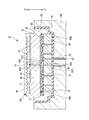
- FIG. 2 is a cross-sectional view schematically showing the electrostatic chuck device 2 of the second embodiment.
- the cooling base portion 60 has a first recess 61.
- At least the first adhesive layer 30 and the second ceramic plate 40 are fitted in the first recess 61.
- the first ceramic plate 10 has a bank portion 18 that surrounds the periphery of the second surface 10b.
- a second ceramic plate 40 is further fitted into the second recess 17 formed by the bank portion 18 and the second surface 10 b via a first adhesive layer 30. That is, the second recess 17 is formed in the second surface 10 b of the first ceramic plate 10.
- the electrostatic chuck device 2 of the second embodiment is different from the electrostatic chuck device 1 of the first embodiment in that the first concave portion 61 and the second concave portion 17 are provided.
- the electrostatic chuck device is doubly fitted, but only one of the fitting structures may be used. Therefore, the cooling base 60 may have only the structure in which the first recess 61 is provided and the second ceramic plate 40 and the first adhesive 30 are fitted. Alternatively, the first ceramic plate 10 may have the second concave portion 17, and only the structure in which the second ceramic plate 40 is fitted to the second concave portion 17 via the first adhesive layer 30 may be used. .
- the second ceramic plate 40 is fitted into the second recess 17 of the first ceramic plate 10, and a part of the second ceramic plate 40 protrudes from the bank portion 18 of the first ceramic plate 10. ing.
- the second ceramic plate 40 is completely fitted into the first ceramic plate 10 to cool the bank portion 18 of the first ceramic plate 10.
- the base-side surface 18b and the back surface 40b of the second ceramic plate 40 on the cooling base portion 60 side may be in the same plane.
- the back surface 40b of the second ceramic plate 40 on the cooling base portion 60 side may be recessed with respect to the cooling base side surface 18b of the bank portion 18 of the first ceramic plate 10.
- the depth of the first recess 61 of the cooling base portion 60 is set so that the placement surface 10a of the plate-like sample W of the first ceramic plate 10 is not positioned lower than the surface 61a of the cooling base portion 60 on which plasma is irradiated. It is preferable to do. That is, it is preferable that the electrostatic chuck device 2 does not have a structure completely embedded in the cooling base portion.
- the depth of the second recess 17 of the first ceramic plate 10 is preferably less than half the thickness of the support plate 12. If the depth of the second concave portion 17 of the first ceramic plate 10 is too deep, it is difficult to maintain the strength of the support plate 12. On the other hand, if the depth of the support plate 12 is too shallow, a part of the first adhesive layer 30 may be exposed in an environment where plasma is irradiated, which is not preferable. Moreover, it is preferable that the thickness of the 1st ceramic plate 10 in this case is 3.0 mm or more and 7.0 mm or less.
- the thickness of the first ceramic plate 10 means the thickness of the portion having the maximum thickness from one surface of the first ceramic plate 10 to the other surface.
- the thermal expansion coefficient of the 2nd ceramic plate 40 fitted is below the thermal expansion coefficient of the 1st ceramic plate 10.
- the thermal expansion coefficient of the second ceramic plate 40 is equal to or higher than the thermal expansion coefficient of the first ceramic plate 10
- the first ceramic plate 10 may be damaged. This is because the second ceramic plate 40 becomes larger than the size of the second recess 17 of the fitted first ceramic plate 10 due to expansion.
- the first ceramic plate 10 is adjacent to the heating member 20 and is further irradiated with plasma, the temperature of the second ceramic plate 40 does not become higher than that of the first ceramic plate 10. Therefore, even if the first ceramic plate 10 and the second ceramic plate 40 have the same thermal expansion coefficient, the first ceramic plate 10 has a higher expansion coefficient. Therefore, the first ceramic plate 10 and the second ceramic plate 40 may have the same coefficient of thermal expansion.
- the second adhesive layer 50 is provided so that the cooling base portion 60 extends along the first concave portion 61 and covers the top surface of the cooling base portion. Since the second adhesive layer covers the fitting portion with the first recess 61, the first adhesive layer 30 can be prevented from being exposed to the surrounding environment. That is, the deterioration of the first adhesive layer 30 can be suppressed. Further, the second ceramic plate 40 and the first adhesive 30 can be firmly fitted in the first recess 61 of the cooling base 60.
- the electrostatic chuck device 2 of the second embodiment even if there is a difference in the thermal expansion coefficient between the first ceramic plate and the second ceramic plate and the cooling base portion, it is positioned by fitting. Generation
- difference etc. can be suppressed. Further, it is possible to suppress the exposure of the first adhesive layer and the second adhesive layer on the surface irradiated with plasma in the process such as etching, and the first adhesive layer and the second adhesive layer are consumed due to deterioration or the like. Can be suppressed.
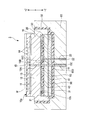
- FIG. 3 is a cross-sectional view schematically showing the electrostatic chuck device 3 of the third embodiment.
- the electrostatic chuck device 3 of the third embodiment is that the plurality of auxiliary heating members 70 are fixed to the one surface 40a of the second ceramic plate 40 on the first ceramic plate 10 side. Different from the electric chuck device 1.
- the auxiliary heating member 70 is fixed to the one surface 40 a of the second ceramic plate 40 on the first ceramic plate 10 side through the adhesive layer 71.
- the auxiliary heating member 70 is a band-shaped member made by meandering a narrow band-shaped metal material like the heating member 20.
- the auxiliary heating member 70 is a member for compensating for the non-uniformity of heat generated in the heating member 20 and includes a plurality of members.
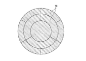
- the plurality of auxiliary heating members 70 can be arranged, for example, for each of the 10 divided regions as shown in FIG. 4 when viewed from the placement surface side of the plate-like sample W.
- the heating member 20 when it is concentrically divided, it is preferable to have a configuration in which several concentric regions are radially divided as shown in FIG. In FIG. 4, the placement surface is divided into ten and the auxiliary heating member 70 is arranged for each region.
- the present invention is not limited to this configuration, and may be divided into a plurality of parts or a smaller number of divisions. .
- the plurality of auxiliary heating members 70 can be controlled independently. Further, the auxiliary heating member 70 may be configured in a multilayer insulated from each other.
- region may differ for every layer.
- the auxiliary heating member 70 is configured in multiple layers and the regions divided by the respective layers are different, the boundary portions of the regions that cannot be auxiliary heated by one layer can be compensated for each other. Since the electrostatic chuck device 3 includes the auxiliary heating member 70, it is possible to improve the temperature uniformity within the surface of the plate-like sample W placed on the electrostatic chuck device 3.
- Each of the plurality of auxiliary heating members 70 can be controlled independently.
- the power supply amount per unit area supplied to each of the plurality of auxiliary heating members 70 is preferably 1/5 or less of the power supply amount per unit area of the heating member 20.
- the adhesive layer 71 is close to the heating member 20 and contacts the auxiliary heating member 70. Therefore, it has high temperature heat resistance of 200 ° C. or higher.
- a polyimide sheet can be used as the adhesive layer 70.
- the adhesive layer 71 may be formed on the entire surface of the second ceramic plate 40, or may be formed only at a location where the auxiliary heating member 70 is formed.
- FIG. 5 is a schematic cross-sectional view of the auxiliary heating member 70.
- the auxiliary heating member 70 includes an energization wiring 76 and a heat generation wiring 77 with an insulating layer (adhesive layer 71) interposed therebetween. Since FIG. 5 is a schematic cross-sectional view, the heat generating wiring 77 is illustrated as being divided. However, the heat generating wiring 77 is formed by meandering strip-shaped metal material, and is integrated in a plan view.
- the energization wiring 76 and the heat generation wiring 77 are electrically connected via the connection portion 78. Therefore, electricity supplied from the energization terminal 74 flows into the energization wiring 76 and is supplied to the heat generation wiring 77 through the connection portion 78.
- the heat generation wiring 77 generates heat when electricity flows.
- An extraction terminal 72 is connected to the heat generation wiring 77 via a connection portion 78, and the auxiliary heating member 70 constitutes one circuit.
- the adhesive layer 71 can also serve as an insulating layer constituting the auxiliary heating member 70.
- a metal having high electrical conductivity such as copper can be used as the energization wiring 76 of the auxiliary heating member 70, and a metal similar to that of the heating member 20 can be used for the heat generation wiring 77. Of these, Ti is preferably used.
- the energizing terminal 74 and the extraction terminal 72 may be covered with insulators 73 and 75 in order to maintain insulation with the cooling base portion 60.
- the heat unevenness generated by the heating member can be compensated by the auxiliary heating member. That is, the thermal uniformity of the electrostatic chuck device can be improved.
- FIG. 6 is a cross-sectional view schematically showing the electrostatic chuck device 4 of the fourth embodiment.
- the electrostatic chuck device 4 of the fourth embodiment includes a plurality of members from which the heating member 20 is separated, each of which is individually Can be controlled.
- the electrostatic chuck device 1 of the first embodiment is that the second ceramic plate 40 is divided in a heat transfer manner in accordance with a region where the temperature of the separated heating member 20 can be individually controlled. And different.
- heat transfer is a state in which the heat transfer between regions that can be controlled is lower than the heat transfer in the region (intermediate of a material having a lower thermal conductivity than the groove or the ceramic plate between the regions). ), Not necessarily when the ceramic plate is divided.
- the heat conduction in the in-plane direction can be controlled, and the temperature controllability for each independently controlled region can be enhanced.
- heat conduction in the in-plane direction is allowed in the concentric direction (circumferential direction), but the heat conduction in the radial direction can be a factor in inhibiting thermal uniformity, so the regions are concentrically divided. It is preferable to do.
- the same material as that of the first adhesive layer 30 can be used for the heat insulating layer 41.
- the material constituting the first adhesive layer 30 can be used as the heat insulating layer 41.
- the heat insulation layer 41 is arrange
- the temperature of the separated heating member can be controlled for each region, and the thermal uniformity of the electrostatic chuck device can be improved.
- the second ceramic plate is divided in a heat transfer manner in accordance with this region, heat conduction in the in-plane direction is suppressed through the second ceramic plate, and the temperature controllability for each region. Can be further enhanced.
- FIG. 7 is a cross-sectional view schematically showing the electrostatic chuck device 5 of the fifth embodiment.
- a third adhesive layer 80 having higher heat resistance than the second adhesive layer 50 is interposed between the second ceramic plate 40 and the second adhesive layer 50.
- the electrostatic chuck apparatus 1 of the first embodiment is different in that one or more ceramic plates 90 are interposed between the second ceramic plate 40 and the second adhesive layer 50.
- FIG. 7 a structure in which the third adhesive layer 80 and the ceramic plate 90 are both interposed between the second ceramic plate 40 and the second adhesive layer 50 is illustrated, but a configuration in which only one of them is interposed is also possible. good.
- the second adhesive layer 50 can be prevented from becoming high temperature. If the temperature of the second adhesive layer 50 does not increase, the second adhesive layer 50 can maintain the adhesiveness and can suppress the occurrence of misalignment or the like.
- the third adhesive layer 80 is disposed at a position closer to the heating member 20 than the second adhesive layer 50, it is considered that the temperature becomes high. Therefore, it is preferable that the heat resistance is higher than that of the second adhesive layer 50.
- the third adhesive layer 80 only needs to satisfy this condition, and for example, a polyimide resin or the like can be used.
- the ceramic plate 90 is preferably made of a material having poor heat transfer properties. For example, mullite (aluminum silicate mineral) or the like can be used. Since the heat transfer coefficient of the ceramic plate 90 is poor, the second adhesive layer 50 can be prevented from becoming high temperature. When a plurality of ceramic plates 90 are present, it is preferable that the ceramic plates 90 be bonded via an adhesive layer 91 or the like having higher heat resistance than the second adhesive layer 50.
- the ceramic plate 90 may have a structure divided for each region, like the second ceramic plate 40 of the fourth embodiment. In order to improve the temperature controllability of the region heated by the auxiliary heating member 70, it is preferable to separate according to the separated shape of the second ceramic plate 40 of the fourth embodiment.
- the plate-like mounting plate 11 and the support plate 12 are produced from an aluminum oxide-silicon carbide (Al 2 O 3 —SiC) composite sintered body or an yttrium oxide (Y 2 O 3 ) sintered body.
- Al 2 O 3 —SiC aluminum oxide-silicon carbide
- Y 2 O 3 yttrium oxide
- a mixed powder containing silicon carbide powder and aluminum oxide powder or yttrium oxide powder is formed into a desired shape, and then, for example, at a temperature of 1400 ° C. to 2000 ° C. in a non-oxidizing atmosphere, preferably an inert atmosphere.
- the mounting plate 11 and the support plate 12 can be obtained by baking for a predetermined time.
- the support plate 12 is formed with one or a plurality of holes for fitting and holding the extraction electrodes 15A of the internal electrode terminals 15.
- the extraction electrode 15 ⁇ / b> A is manufactured so as to have a size and shape that can be tightly fixed to the fixing hole of the support plate 12.
- a method for producing the extraction electrode 15A for example, when the extraction electrode 15A is made of a conductive composite sintered body, a method of forming a conductive ceramic powder into a desired shape and pressurizing and firing can be cited.
- the conductive ceramic powder used for the extraction electrode 15A is preferably a conductive ceramic powder made of the same material as the internal electrode 13 for electrostatic adsorption.
- a high melting point metal is used, and a method of forming by a metal processing method such as a grinding method or powder metallurgy, or the like can be used.
- an internal electrode for electrostatic adsorption in which a conductive material such as the above-mentioned conductive ceramic powder is dispersed in an organic solvent so as to come into contact with the extraction electrode 15A in a predetermined region on the surface of the support plate 12 in which the extraction electrode 15A is fitted.
- the coating liquid is applied and dried to form the electrostatic adsorption internal electrode 13.
- this coating method it is desirable to use a screen printing method or the like because it is necessary to apply the film to a uniform thickness.
- Other methods include forming a thin film of the above-mentioned refractory metal by vapor deposition or sputtering, or arranging an electroconductive ceramic or refractory metal thin plate to provide an internal electrode for electrostatic adsorption. 13 or the like.
- the same composition as the mounting plate 11 and the support plate 12 is used.
- an insulating material layer including a powder material having the same main component is formed.
- the insulating material layer is formed by applying a coating solution in which an insulating material powder having the same composition or the same main component as the mounting plate 11 and the support plate 12 is dispersed in an organic solvent by screen printing or the like, and drying the coating. Can be formed.
- the mounting plate 11 is superposed on the electrostatic adsorption internal electrode 13 and the insulating material layer on the support plate 12, and these are integrated by hot pressing under high temperature and high pressure.
- the atmosphere in this hot press is preferably a vacuum or an inert atmosphere such as Ar, He, N 2 or the like.
- the pressure during uniaxial pressing in the hot press is preferably 5 MPa to 10 MPa, and the temperature is preferably 1400 ° C. to 1850 ° C.
- the electrostatic adsorption internal electrode 13 is fired to become the electrostatic adsorption internal electrode 13 made of a conductive composite sintered body.
- the support plate 12 and the mounting plate 11 are joined and integrated.
- the electrostatic adsorption internal electrode 13 is refired by hot pressing under high temperature and high pressure, and is closely fixed to the fixing hole of the support plate 12. Then, the upper and lower surfaces, outer periphery, gas holes, and the like of these joined bodies are machined to form the first ceramic plate 10.
- the second surface 10b of the first ceramic plate 10 is rotary-cut or the like.
- the second concave portion 17 can be produced by cutting with.
- An adhesive layer 21 such as polyimide resin is attached to a predetermined region of the second surface 10b of the first ceramic plate 10.
- a non-magnetic material such as a titanium (Ti) thin plate, a tungsten (W) thin plate, a molybdenum (Mo) thin plate, or the like having a constant thickness of 0.2 mm or less, preferably 0.1 mm or less, on the adhesive layer 21.
- a thin metal plate is attached, and this non-magnetic thin metal plate is etched into a desired heater pattern by photolithography to obtain a heating member 20.
- the heating member 20 having a desired heater pattern is formed on the second surface 10b of the first ceramic plate 10.
- the second ceramic plate 40 is produced.
- an alumina (Al 2 O 3 ) sintered body is formed into a plate shape, and the second ceramic plate 40 is produced.
- the second ceramic plate 40 can be obtained by forming the aluminum oxide powder into a desired shape and then firing it for a predetermined time.
- a through hole for inserting the first lead electrode 15C of the internal electrode terminal 15 and the power supply terminal 22 is formed in the second ceramic plate 40.
- the size of the through hole is made so that the first lead electrode 15C and the power supply terminal 22 can be tightly fixed.
- a method for producing the first lead electrode 15C and the power supply terminal 22 for example, when the power supply terminal 22 is a conductive composite sintered body, a method of forming a conductive ceramic powder into a desired shape and performing pressure firing Etc.
- the second ceramic plate 40 When the second ceramic plate 40 is divided into a plurality of parts through the heat insulating layer 41, the second ceramic plate 40 can be manufactured by the following procedure. A plate made of the same material as the second ceramic plate 40 is prepared, and an uneven shape is formed on the surface thereof by end milling, blasting, or the like. The formed concave and convex portions are filled with a material constituting the heat insulating layer 41 and cured. Then, the 2nd ceramic plate 40 divided
- the auxiliary heating member 70 on the one surface 40a of the second ceramic plate 40 on the first ceramic plate 10 side it can be produced by the following procedure.
- the energization wiring 76 is formed on one surface of the second ceramic plate 40.
- the formation of the conductive wiring 76 is not particularly limited, but can be realized by vapor deposition, sputtering, or the like of a metal film through a mask. Alternatively, pattern etching may be performed after vapor deposition or sputtering.
- an adhesive layer (insulating layer) 71 such as polyimide resin is attached.
- a metal to be the heat generating wiring 77 is vapor-deposited or sputtered through a mask.
- the energization terminal 74 and the extraction terminal 72 can be manufactured by the same method as that of the power supply terminal 22.
- the electrostatic chuck device further includes the ceramic plate 90 between the second ceramic plate 40 and the cooling base portion 60, the ceramic is interposed on the one surface of the second ceramic plate 40 via the adhesive layer 91 in advance.
- the plate 90 is preferably adhered.
- the first ceramic plate 10 to which the heating member 20 is bonded and the second ceramic plate 40 are bonded.
- the extraction electrode 15A and the first extraction electrode 15C are electrically connected by the first conductive adhesive 15B.
- a material constituting the first adhesive layer 30 made of, for example, polyimide resin is applied to the second surface 10b of the first ceramic plate 10 after the spacer 31 is disposed. After coating the material constituting the first adhesive layer 30, the one surface 40a of the second ceramic plate 40 is pressed and heated.
- the material which comprises the 1st contact bonding layer 30 hardens
- a metal material made of aluminum (Al), aluminum alloy, copper (Cu), copper alloy, stainless steel (SUS), etc. is machined, and if necessary, a flow of refrigerant flowing inside the metal material A path or the like is formed, and the cooling base portion 60 is produced. It is preferable that at least the surface of the cooling base portion 60 exposed to plasma is subjected to an alumite treatment or an insulating film such as alumina is formed. Next, a through hole through which the second extraction electrode 15 ⁇ / b> E of the internal electrode terminal 15, the power supply terminal 22, the energization terminal 74 and the extraction terminal 72 are inserted is formed in the cooling base portion 60.
- the 1st recessed part 61 can be produced by cutting by rotary grinding etc. similarly to the 2nd recessed part 17 of the 1st ceramic plate 10.
- the second adhesive layer 50 is applied to one surface of the cooling base portion 60, and the first ceramic plate 10 and the second ceramic plate 40 that have already been formed on the coated surface have the heating member 20 interposed therebetween.
- the material constituting the second adhesive layer 50 is cured, and these can be bonded.
- the first lead electrode 15C and the second lead electrode 15E are electrically connected by a second conductive adhesive 15D.
- the electrostatic chuck device of the example has the same configuration as the electrostatic chuck device 1 of the first embodiment shown in FIG.
- the shapes of the first ceramic plate, the heating member, and the second ceramic plate are circular and have a diameter of 300 mm.
- the shape of the cooling base is circular and has a diameter of 400 mm.
- As the first ceramic plate an aluminum oxide-silicon carbide (Al 2 O 3 —SiC) composite sintered body was used.
- the thickness of the ceramic plate is 3 mm.
- the heating member was composed of a plurality of members separated and independent from each other, and a titanium (Ti) thin plate was used.
- the heating member has a thickness of 0.1 mm.
- the electrostatic chuck device is configured from the heating member side as the first adhesive layer, the second ceramic plate, the third adhesive layer, the second adhesive layer, and the cooling base portion. Cooling water was passed through a chiller on the side opposite to the heating member (not shown).
- the first adhesive layer is a polyimide resin
- the second ceramic plate is an alumina (Al 2 O 3 ) plate
- the third adhesive layer is a polyimide sheet
- the second adhesive layer is a silicone resin
- the temperature of the heating member was 300 ° C., and the temperature of the chiller was 100 ° C.
- the first ceramic plate was ignored because it did not significantly affect the temperature between the heating member and the cooling base.
- the thickness of each member is 0.2 mm for the first adhesive layer, 1.5 mm for the second ceramic plate, 0.1 mm for the third adhesive layer, 0.2 mm for the second adhesive layer, and the cooling base portion. It was 5.0 mm.
- the temperature that each member can take by transferring heat to the cooling base portion was calculated and summarized in Table 1 below.
- the temperature of the second adhesive layer is as low as 116 to 164 ° C.
- first adhesive layer 31 ... Spacer, 40 ... second ceramic plate, 40a ... one side, 40b ... back side, 50 ... second adhesive layer, 60 ... Cooling base part, 61 ... 1st recessed part, 70 ... auxiliary heating member, 71 ... Adhesive layer (insulating layer), 72 ... Extraction terminal, 73 ... Reiko, 74: Energizing terminal, 75 ... Reiko, 76 ... energization wiring, 77 ... Heat generation wiring, 78 ... connection part, 80 ... a third adhesive layer, 90 ... Ceramic plate, 91 ... Adhesive layer
Landscapes
- Container, Conveyance, Adherence, Positioning, Of Wafer (AREA)
Abstract
Description
本願は、2014年11月20日に、日本に出願された特願2014―235455号に基づき優先権を主張し、その内容をここに援用する。
このような静電チャック装置は、その使用温度が200℃以下であることが、一般的である(例えば、特許文献2及び特許文献3)。例えば、特許文献3には、200℃以下の温度領域で用いることができる接着層としてシリコーン系の樹脂組成物が記載されている。
一方で、柔軟性を有する高温領域に耐熱性を有さない接着層は、耐熱性が十分では無いため、例えば200℃以上等の高温環境下では溶解または分解してしまう。そのため、耐熱性が十分ではない接着層を用いた場合も、ベース部にセラミック基体を十分に固定することができず、位置ずれ等が生じる。
したがって、上記構成を用いることで、高温環境下でも使用することが可能な耐熱性の高い静電チャック装置を提供することができる。
なお、以下の説明で用いる図面は、本発明の特徴をわかりやすくするために便宜上特徴となる部分を拡大して示している場合があり、各構成要素の寸法比率などは実際とは異なっていることがある。また、以下の説明において例示される材料、寸法等は一例であって、本発明はそれらに限定されるものではなく、その要旨を変更しない範囲で適宜変更して実施することが可能である。
図1は、第1実施形態の静電チャック装置1を模式的に示す断面図である。
第1実施形態にかかる静電チャック装置1は、板状試料Wを載置できる第1の面10aとその反対側の第2の面10bを有し、静電吸着用内部電極13を内蔵してなる第1のセラミックプレート10と、第2の面10bに固定された加熱部材20と、第1のセラミックプレート10及び加熱部材20に、第1の接着層30を介して接着された第2のセラミックプレート40と、第2のセラミックプレート40に第2の接着層50を介して接着された冷却ベース部60とを有する。すなわち、図1の+Z方向に、冷却ベース部60、第2の接着層50、第2セラミックプレート40、第1の接着層30、加熱部材20、第1のセラミックプレート10がこの順に積層された構造を有する。
<第1のセラミックプレート>
第1のセラミックプレート10は、半導体ウエハ、金属ウエハ、ガラス基材等の板状試料Wを載置する載置板11と、この載置板11に対向配置された支持板12と、載置板11と支持板12の間に挟まれた静電吸着用内部電極13を有する。
また第1のセラミックプレート10は、板状試料Wを載置する第1の面10aと、その反対側の第2の面10bとを有する。
支持板12には、厚さ方向に貫通する孔が設けられている。この孔には、内部電極端子15が挿通する。
静電吸着用内部電極13の材料は載置板11及び支持板12に使用する材料との熱膨張差や耐熱性などを考慮して選定される。例えば、静電吸着用内部電極13は、酸化アルミニウム-炭化タンタル(Al2O3-Ta4C5)導電性複合焼結体、酸化アルミニウム-タングステン(Al2O3-W)導電性複合焼結体、酸化アルミニウム-炭化ケイ素(Al2O3-SiC)導電性複合焼結体、窒化アルミニウム-タングステン(AlN-W)導電性複合焼結体、窒化アルミニウム-タンタル(AlN-Ta)導電性複合焼結体、酸化イットリウム-モリブデン(Y2O3-Mo)導電性複合焼結体等の導電性セラミックス、あるいは、タングステン(W)、タンタル(Ta)、モリブデン(Mo)等の高融点金属や、銀(Ag)、炭素(C)等を使用することができる。
厚みが0.1μmを下回ると、充分な導電性を確保することができず、一方、厚みが100μmを越えると、この静電吸着用内部電極13と載置板11及び支持板12との間の熱膨張率差に起因して、この静電吸着用内部電極13と載置板11及び支持板12との接合界面にクラックが入り易くなるからである。
このような厚みの静電吸着用内部電極13は、スパッタ法や蒸着法等の成膜法、あるいはスクリーン印刷法等の塗工法により容易に形成することができる。
内部電極端子15のうち取出し電極15A、第1引き出し電極15C、第2引き出し電極15Eの材料は、耐熱性に優れた導電性材料であれば特に制限されるものではないが、熱膨張係数が静電吸着用内部電極13、支持板12及び後述する第2のセラミックプレートの熱膨張係数に近似したものが好ましい。例えば、静電吸着用内部電極13を構成している導電性セラミックス、あるいは、タングステン(W)、タンタル(Ta)、モリブデン(Mo)、ニオブ(Nb)、コバール合金等の金属材料が好適に用いられる。第1導電性接着材15Bは、耐熱性を有する必要がある。そのため、導電性フィラー等を用いて導電性が付与されたポリイミド樹脂等を好適に用いることができる。第2導電性接着材15Dは、柔軟性が必要となるため、導電性フィラー等を用いて導電性が付与されたシリコーン樹脂等を好適に用いることができる。このように、取出し電極15A、第1引き出し電極15C及び第2引き出し電極15Eを、第1導電性接着材15B及び第2導電性接着材15Dで繋ぐことで、静電吸着用内部電極13から内部電極端子15が熱応力により外れてしまうことを抑制することができる。
加熱部材20は、第1のセラミックプレート10の第2の面10bに接着層21を介して所定のパターンで配設固定されている。加熱部材20は、幅の狭い帯状の金属材料を蛇行させた1つの連続した帯状の部材である。帯状の部材の両端部には、図1で示す給電用端子22が溶接等により接続され、給電端子22は、絶縁性を有する碍子23により冷却ベース部60に対して絶縁されている。なお、給電用端子22は 第2のセラミックプレート40と冷却ベース部60との熱膨張差を緩和できる、金属製のより線等による柔構造部(図視略)を有している。
加熱部材20の厚みが0.2mmを超えると、加熱部材20のパターン形状が板状試料Wの温度分布として反映され、板状試料Wの面内温度を所望の温度パターンに維持することが困難になる。
また、加熱部材20を一定の厚みとすることで、加熱部材20の発熱量も加熱面全域で一定とすることができる。これにより、第1のセラミックプレート10の第1の面10aにおける温度分布を均一化できる。
加熱部材20を非磁性金属で形成することで、静電チャック装置1を高周波雰囲気中で用いても加熱部材20が高周波により自己発熱しない。したがって、高周波雰囲気中であっても、板状試料Wの面内温度を所望の一定温度または一定の温度パターンに維持することが容易となる。
接着層21は、シート状またはフィルム状の接着性樹脂である。加熱部材20に直接接触する部分であり、200℃以上の高熱となるため高い耐熱性が必要であり、絶縁性を有するものであることが好ましい。そのため、ポリイミド樹脂等を採用することができる。
接着層21の厚みは5μm以上100μm以下が好ましく、10μm以上50μm以下であることがより好ましい。この接着層21の厚みが10μm以上の場合、接着層21の面内の厚みのバラツキは10μm以内が好ましい。接着層21の面内の厚みのバラツキが10μmを超えると、第1のセラミックプレート10と加熱部材20との面内間隔に10μmを超えるバラツキが生じる。その結果、加熱部材20から第1のセラミックプレート10に伝達される熱の面内均一性が低下し、第1のセラミックプレート10の載置面における面内温度が不均一となる虞がある。
第1の接着層30は、第1のセラミックプレート10及び加熱部材20と第2のセラミックプレート40の間に介在する。第1の接着層30は、第1のセラミックプレート10及び加熱部材20と第2のセラミックプレート40を接着一体化する。また、第1の接着層30は、第1のセラミックプレート10及び加熱部材20と第2のセラミックプレート40のそれぞれの熱膨張率差に起因して、第1のセラミックプレート10及び加熱部材20と第2のセラミックプレート40との界面に生じる熱応力を緩和する。
この熱応力は、第1のセラミックプレート10及び第2のセラミックプレート40の熱膨張率差に起因して生じる。しかしながら、第1のセラミックプレート10及び第2のセラミックプレート40は互いにセラミックであるため、それぞれの熱膨張率にそれほど大きな差はない。そのため、第1の接着層30に柔軟性が低い材料を用いても、十分高い接着性を維持することができ、位置ずれ等の問題を生じさせない。
このような耐熱性を有し、第1のセラミックプレート10と第2のセラミックプレート40間に生じる応力を緩和できる第1の接着層を構成する材料としては、例えば、ポリイミド樹脂等を採用できる。
第1の接着層30の厚みが薄すぎると、加熱部材20で生じた熱がすぐに第2のセラミックプレート40に伝達し、冷却ベース部60に至るまでに十分温度を低下することが難しくなる。一方で、第1の接着層30の厚みが厚くなると、第1の接着層30の柔軟性が低い場合に、硬く厚い層が接着界面に形成されることとなるため、応力により生じる歪を十分に緩和することができなくなり、位置ずれや剥離等の問題を生じる恐れが高くなる。
また第1の接着層30の厚みが厚くなると、冷却ベース部60への熱伝達性が低下するため、冷却特性に劣化が生じる。
第1の接着層30の熱伝導率の具体的な値としては、0.10W/mK~0.50W/mKであることが好ましい。
スペーサー31は、特に制限されるものではないが、第1の接着層30との熱膨張率差に伴う応力の発生及び熱伝導率差による局所的な温度ムラの発生を抑制する観点より、接着層30と熱膨張率及び熱伝導率が近似し、高温でも高い剛性率を有するポリイミド等を用いることが好ましい。
第2のセラミックプレート40は、第1のセラミックプレート10及び加熱部材20に、第1の接着層30を介して接着される。
第2の接着層50は、第2のセラミックプレート40と冷却ベース部60の間に介在する。第2の接着層50は、第2のセラミックプレート40と冷却ベース部60を接着一体化する。また第1のセラミックプレート10及び加熱部材20と第2のセラミックプレート40の熱膨張率差に起因して生じる、第1のセラミックプレート10及び加熱部材20と第2のセラミックプレート40界面の熱応力を緩和する。
冷却ベース部60は、第2のセラミックプレート40と第2の接着層50を介して接着し、少なくとも第2のセラミックプレート40を冷却する。第2のセラミックプレート40を冷却することで、第2のセラミックプレート40に接着された第1のセラミックプレート10及び板状試料Wを所望の温度に調整することができる。
冷却ベース部60としては、例えば、内部に冷媒を流動させる流路(図示略)が形成された液冷ベース等が好適である。
冷却ベース部60を構成する材料としては、熱伝導性、導電性、加工性に優れた金属、またはこれらの金属を含む複合材であれば特に制限はなく、例えば、アルミニウム(Al)、アルミニウム合金、銅(Cu)、銅合金、ステンレス鋼(SUS) 等が好適に用いられる。冷却ベース部50の少なくともプラズマに曝される面は、アルマイト処理が施されているか、あるいはアルミナ等の絶縁膜が成膜されていることが好ましい。
また、第2の接着層50は、加熱部材20から遠く、冷却ベース部60に近い構成とすることができるため、第2の接着層50が劣化することを抑制することができる。また第2の接着層50のヤング率は、第1の接着層30のヤング率よりも小さいため、第2のセラミックプレート40と冷却ベース部60の熱膨張率差が大きくても、十分応力緩和することができる。
したがって、上記構成を用いることで、200℃以上の高温でも使用することが可能な耐熱性の高い静電チャック装置1を提供することができる。
図2は、第2実施形態の静電チャック装置2を模式的に示す断面図である。第2の実施形態の静電チャック装置2は、冷却ベース部60が第1凹部61を有する。第1凹部61には、少なくとも第1の接着層30及び第2のセラミックプレート40が嵌合されている。また第1のセラミックプレート10は、第2の面10bの周囲を囲む土手部18を有する。この土手部18及び第2の面10bによって形成される第2凹部17には、さらに第1の接着層30を介して第2のセラミックプレート40が嵌合されている。
すなわち、第1のセラミックプレート10の第2の面10bに、第2凹部17が形成されている。さらにこの第2凹部17に、加熱部材20及び第1の接着層50を介して、第2のセラミックプレート40が嵌合され一体化した部材が形成されている。そして、この一体化した部材が、冷却ベース部60の第1凹部61に嵌合されている。したがって、第2の実施形態の静電チャック装置2は、第1凹部61及び第2凹部17を有している点が第1の実施形態の静電チャック装置1と異なっている。
またこの場合の第1のセラミックプレート10の厚みは、3.0mm以上7.0mm以下であることが好ましい。ここで第1のセラミックプレート10の厚みとは、第1のセラミックプレート10の一方の面からもう一方の面までの最大の厚みを有している部分の厚みを意味する。3.0mm以上であれば、第2凹部17が形成されても十分な強度を維持することができる。一方、7.0mm以下であれば、第1のセラミックプレート10の熱容量が大きくなり過ぎて、載置される板状試料Wの熱応答性が劣化する。
ここで、第1のセラミックプレート10は加熱部材20に隣接し、さらにプラズマ照射されるため、第2のセラミックプレート40の温度が、第1のセラミックプレート10より高くなることは無い。そのため、第1のセラミックプレート10と第2のセラミックプレート40の熱膨張率が同一でも、膨張率は第1のセラミックプレート10の方が大きくなる。したがって、第1のセラミックプレート10と第2のセラミックプレート40の熱膨張率は同一でもよい。
図3は、第3実施形態の静電チャック装置3を模式的に示す断面図である。第3実施形態の静電チャック装置3は、第2のセラミックプレート40の第1セラミックプレート10側の一面40aに、複数の補助加熱部材70が固定されている点が、第1実施形態の静電チャック装置1と異なる。
補助加熱部材70は、接着層71を介して、第2のセラミックプレート40の第1セラミックプレート10側の一面40aに固定されている。補助加熱部材70は、加熱部材20と同様に幅の狭い帯状の金属材料を蛇行させた帯状の部材である。補助加熱部材70は、加熱部材20で生じた熱の不均一を補償するための部材であり、複数の部材からなる。
複数の補助加熱部材70は、板状試料Wの載置面側から平面視した際に、例えば、図4のように10分割された領域毎に配置することができる。特に、加熱部材20が同心円状に分割されている場合は、図4に示すように同心円状の領域を径方向にいくつか分割した構成とすることが好ましい。また図4では、載置面を10分割して領域毎に補助加熱部材70を配置しているが、当該構成に限られず、より複数に分割してもよく、またより少ない分割数としてもよい。これらの複数の補助加熱部材70はそれぞれ独立して制御することができる。また補助加熱部材70は互いに絶縁された多層に構成されていてもよい。また層毎に、分割されている領域が異なっていてもよい。補助加熱部材70が多層に構成され、かつそれぞれの層で分割されている領域が異なっている場合、一層では補助加熱できなかった領域毎の境界部分を互いに補償することができる。
静電チャック装置3は、補助加熱部材70を有するため、静電チャック装置3に載置される板状試料Wの面内の温度均一性を高めることができる。
補助加熱部材70に電力を供給することで、電力が供給された領域が、冷却ベース部60により冷却されることを制限することができる。その結果、補助加熱部材70に電力を供給した領域の温度が下がりにくくなり、面内の均熱性を制御することができる。すなわち、補助加熱部材70は、温度変化を制御できる程度の電力を供給すれば機能することができ、加熱部材70程の電力供給量を要しない。したがって、補助加熱部材70は、加熱部材20ほど高温になることは無い。
図5は、補助加熱部材70の断面模式図を示す。補助加熱部材70は、絶縁層(接着層71)を挟んで、通電配線76と発熱配線77を有する。図5は断面模式図であるため、発熱配線77が分断されているように図示されているが、発熱配線77は帯状の金属材料が蛇行してなり、平面視では一体となっている。通電配線76と発熱配線77は、接続部78を介して、電気的に接続されている。そのため、通電端子74から供給された電気が、通電配線76に流れ、接続部78を介して発熱配線77に供給される。発熱配線77は、電気が流れることで発熱する。発熱配線77には、接続部78を介して取出し端子72が接続され、補助加熱部材70が一つの回路を構成している。このとき絶縁層は、高い絶縁性を求められるため、ポリイミドシートを用いることが多い。この場合、接着層71は補助加熱部材70を構成する絶縁層を兼ねることもできる。この補助加熱部材70の通電配線76としては、銅等の電気伝導性の高い金属を用いることができ、発熱配線77は加熱部材20と同様の金属を用いることができる。中でもTiを用いることが好ましい。なお、通電端子74、取出し端子72は、冷却ベース部60との絶縁性を維持するため、その周りを碍子73、75で被覆されていてもよい。
図6は、第4実施形態の静電チャック装置4を模式的に示す断面図である。第4実施形態の静電チャック装置4は、第1の実施形態の静電チャック装置1の好ましい例として記載されているように、加熱部材20が分離された複数の部材からなり、それぞれが個々に制御可能である。また、分離された加熱部材20が個々に温度制御可能である領域に合せて、第2のセラミックプレート40が伝熱的に分割されている点も、第1の実施形態の静電チャック装置1と異なる。
ここで、伝熱的に分割とは、制御可能である領域間の熱伝達が、領域内の熱伝達より低い状態をさし(領域間に溝もしくは セラミックプレートより熱伝導率の低い物質の介在)、必ずしもセラミックプレートが分割されている場合に限らない。
図7は、第5実施形態の静電チャック装置5を模式的に示す断面図である。第5実施形態の静電チャック装置5は、第2のセラミックプレート40と第2の接着層50の間に、第2の接着層50より耐熱性の高い第3の接着層80が介在し、さらに第2のセラミックプレート40と第2の接着層50の間に、一つ以上のセラミックプレート90が介在している点が第1実施形態の静電チャック装置1と異なる。
図7では、第2のセラミックプレート40と第2の接着層50の間に、第3の接着層80及びセラミックプレート90が共に介在した構造を図示したが、いずれか一方のみが介在する構成でも良い。
セラミックプレート90が複数介在する場合は、第2の接着層50より耐熱性の高い接着層91等を介して接合していることが好ましい。
次に、この静電チャック装置1の製造方法について説明する。第1実施形態の静電チャック装置1~第5実施形態の静電チャック装置5の製造方法は、第1実施形態の静電チャック装置を基に製造方法を説明し、違いを有する点のみその他の実施例の静電チャック装置について言及する。
取出し電極15Aを金属とした場合、高融点金属を用い、研削法、粉末治金等の金属加工法等により形成する方法等が挙げられる。
この塗布法としては、均一な厚さに塗布する必要があることから、スクリーン印刷法等を用いることが望ましい。また、他の方法としては、蒸着法あるいはスパッタリング法により上記の高融点金属の薄膜を成膜する方法、上記の導電性セラミックスあるいは高融点金属からなる薄板を配設して静電吸着用内部電極13とする方法等がある。
また、ホットプレスにおける一軸加圧の際の圧力は5MPa~10MPaが好ましく、温度は1400℃~1850℃が好ましい。
また、静電吸着用内部電極13は、高温、高圧下でのホットプレスで再焼成され、支持板12の固定孔に密着固定される。
そして、これら接合体の上下面、外周、及びガス穴等を機械加工し、第1のセラミックプレート10とする。
この接着層21上に、厚みが0.2mm以下、好ましくは0.1mm以下の一定の厚みを有する、例えば、チタン(Ti)薄板、タングステン(W)薄板、モリブデン(Mo)薄板等の非磁性金属薄板を貼着し、この非磁性金属薄板をフォトリソグラフィー法により、所望のヒータパターンにエッチング加工し、加熱部材20とする。
これにより、第1のセラミックプレート10の第2の面10bに所望のヒータパターンを有する加熱部材20が形成される。
その後、凹部の底面に沿って、プレートを切断することで、断熱層41を介して複数に分割された第2のセラミックプレート40を作製することができる。
まず第2のセラミックプレート40のいずれか一面に通電配線76を形成する。通電配線76の形成は、特に限定されるものではないが、マスクを介して金属膜を蒸着、スパッタ等することで実現できる。また蒸着やスパッタ等後に、パターンエッチングしてもよい。
次に、ポリイミド樹脂等の接着層(絶縁層)71を貼着する。その後、接着層71の接続部78に対応する箇所に穴を開けた後、発熱配線77となる金属を、マスクを介して蒸着、スパッタ等する。通電端子74及び取出し端子72は、給電端子22と同様の方法で作製することができる。
これらを接着する前に、加熱部材20の接合される面上にスペーサー31を配置し、第1のセラミックプレート10と第2のセラミックプレート40の間隔を予め設定しておくことが好ましい。スペーサー31を配置後の第1のセラミックプレート10の第2の面10bに、例えばポリイミド樹脂からなる第1の接着層30を構成する材料を塗工する。第1の接着層30を構成する材料を塗工後に、第2のセラミックプレート40の一面40aを押し当て、加熱する。加熱により第1の接着層30を構成する材料が硬化し、第1の接着層30が形成される。このようにして、第1のセラミックプレート10と第2のセラミックプレート40が、間に加熱部材20を有した状態で接着された部材が作製される。
この冷却ベース部60の少なくともプラズマに曝される面には、アルマイト処理を施すか、あるいはアルミナ等の絶縁膜を成膜することが好ましい。
次いで、冷却ベース部60に、内部電極端子15の第2取り出し電極15E、給電端子22、通電端子74及び取出し端子72が挿通されるための貫通孔を形成する。
第1のセラミックプレート、加熱部材、第2のセラミックプレートの形状は円形であり、300mm直径を有する。冷却ベース部の形状は円形であり、400mm直径を有する。
第1のセラミックプレートとしでは酸化アルミニウム-炭化ケイ素(Al2O3-SiC)複合焼結体を用いた。セラミックプレートの厚みは3mmである。加熱部材としては分離され相互に独立した複数の部材からなり、チタン(Ti)薄板を用いた。加熱部材は、厚みが0.1mmの厚みを有する。
加熱部材が300℃の温度に加熱された場合において、加熱により生じた熱が冷却ベース部まで伝達する際に各部材が取りうる温度範囲を熱伝達計算により求めた。
このとき、静電チャック装置は、加熱部材側から、第1の接着層、第2のセラミックプレート、第3の接着層、第2の接着層、冷却ベース部と言う構成にし、冷却ベース部の加熱部材と反対側にチラーにより冷却水を通水した(図示略)。
第1の接着層としてはポリイミド樹脂、第2のセラミックプレートとしてはアルミナ(Al2O3)板、第3の接着層としてはポリイミドシート、第2の接着層としてはシリコーン樹脂、冷却ベース部材としてはアルミを用いた。また加熱部材の温度は300℃とし、チラーの温度は100℃とした。なお、第1のセラミックプレートは、加熱部材と冷却ベース部間の温度に大きな影響を与えないため無視した。
各部材の厚みは、第1の接着層が0.2mm、第2のセラミックプレートが1.5mm、第3の接着層が0.1mm、第2の接着層が0.2mm、冷却ベース部が5.0mmとした。このとき、各部材の単位面積当たりの熱伝達率を用いて、熱が冷却ベース部に伝達することによって各部材が取りうる温度を計算し、以下の表1にまとめた。
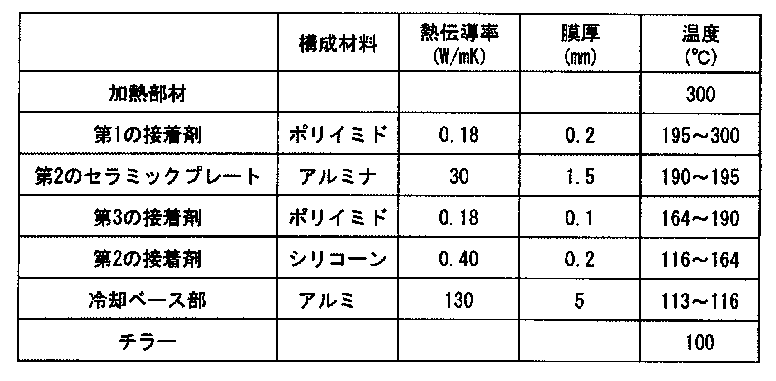
10…第1のセラミックプレート、
10a…第1の面、10b…第2の面、
11…載置板、
12…支持板、
13…静電吸着用内部電極、
14…突起部、
15…内部電極端子、15A…取り出し電極、15B…第1導電性接着材、15C…第1引き出し電極、15D…第2引き出し電極、
16…碍子、
17…第2凹部、
18…土手部、18a…土手部の冷却ベース側の面、
20…加熱部材、
21…接着層、
22…給電端子、
23…碍子、
30…第1の接着層、
31…スペーサー、
40…第2のセラミックプレート、40a…一面、40b…裏面、
50…第2の接着層、
60…冷却ベース部、
61…第1凹部、
70…補助加熱部材、
71…接着層(絶縁層)、
72…取出し端子、
73…碍子、
74…通電端子、
75…碍子、
76…通電配線、
77…発熱配線、
78…接続部、
80…第3の接着層、
90…セラミックプレート、
91…接着層
Claims (10)
- 板状試料を載置できる第1の面とその反対側の第2の面を有し、静電吸着用内部電極を内蔵してなる第1のセラミックプレートと、
前記第2の面に固定された加熱部材と、
前記第1のセラミックプレート及び加熱部材に、第1の接着層を介して接着された第2のセラミックプレートと、
前記第2のセラミックプレートに、第2の接着層を介して接着された冷却ベース部とを有し、
前記第1の接着層が前記第2の接着層より高い耐熱性を有し、
前記第2の接着層のヤング率が、前記第1の接着層のヤング率よりも小さい静電チャック装置。 - 前記第1および2の接着層の熱伝達率が、前記第2のセラミックプレートの熱伝達率の1/2以下である請求項1に記載の静電チャック装置。
- 前記冷却ベース部が第1凹部を有し、少なくとも前記第1の接着層及び前記第2のセラミックプレートが、前記第1凹部に嵌合されている請求項1または2のいずれかに記載の静電チャック装置。
- 前記第1のセラミックプレートが前記第2の面を囲む土手部を有し、
前記土手部及び前記第2の面によって形成される第2凹部に、第1の接着層を介して前記第2のセラミックプレートが嵌合されている請求項1~3のいずれか一項に記載の静電チャック装置。 - 第1のセラミックプレートが、酸化アルミニウム-炭化ケイ素複合焼結体、酸化アルミニウム焼結体、窒化アルミニウム焼結体、または酸化イットリウム焼結体からなることを特徴とする請求項1~4のいずれか一項に記載の静電チャック装置。
- 前記第2のセラミックプレートの前記第1のセラミックプレート側の面に、複数の補助加熱部材が固定され、前記補助加熱部材がそれぞれ個々に温度制御可能である請求項1~5のいずれか一項に記載の静電チャック装置。
- 前記加熱部材が分離された複数の部材からなり、それぞれが個々に温度制御可能である請求項1~6のいずれか一項に記載の静電チャック装置。
- 分離された前記加熱部材が個々に温度制御可能である領域に合せて、前記第2のセラミックプレートが伝熱的に分割されている請求項7に記載の静電チャック装置。
- 前記第2のセラミックプレートと前記第2の接着層の間に、前記第2の接着層より耐熱性の高い第3の接着層が介在する請求項1~8のいずれか一項に記載の静電チャック装置。
- 前記第2のセラミックプレートと第2の接着層の間に、一つ以上のセラミックプレートが介在する請求項1~9のいずれか一項に記載の静電チャック装置。
Priority Applications (2)
| Application Number | Priority Date | Filing Date | Title |
|---|---|---|---|
| JP2015561818A JP6172301B2 (ja) | 2014-11-20 | 2015-11-11 | 静電チャック装置 |
| US15/528,008 US10079167B2 (en) | 2014-11-20 | 2015-11-11 | Electrostatic chucking device |
Applications Claiming Priority (2)
| Application Number | Priority Date | Filing Date | Title |
|---|---|---|---|
| JP2014-235455 | 2014-11-20 | ||
| JP2014235455 | 2014-11-20 |
Publications (1)
| Publication Number | Publication Date |
|---|---|
| WO2016080262A1 true WO2016080262A1 (ja) | 2016-05-26 |
Family
ID=56013804
Family Applications (1)
| Application Number | Title | Priority Date | Filing Date |
|---|---|---|---|
| PCT/JP2015/081732 Ceased WO2016080262A1 (ja) | 2014-11-20 | 2015-11-11 | 静電チャック装置 |
Country Status (3)
| Country | Link |
|---|---|
| US (1) | US10079167B2 (ja) |
| JP (1) | JP6172301B2 (ja) |
| WO (1) | WO2016080262A1 (ja) |
Cited By (13)
| Publication number | Priority date | Publication date | Assignee | Title |
|---|---|---|---|---|
| JP2018006393A (ja) * | 2016-06-28 | 2018-01-11 | 日本特殊陶業株式会社 | 保持装置 |
| WO2018123729A1 (ja) * | 2016-12-26 | 2018-07-05 | 京セラ株式会社 | 試料保持具 |
| JP2020004820A (ja) * | 2018-06-27 | 2020-01-09 | 京セラ株式会社 | 試料保持具 |
| KR20200120093A (ko) * | 2019-04-11 | 2020-10-21 | 고갑석 | 기판 가열장치의 열전달 플레이트 구조 |
| JP2020202352A (ja) * | 2019-06-13 | 2020-12-17 | 新光電気工業株式会社 | 基板固定装置及びその製造方法 |
| JP2021158334A (ja) * | 2020-03-26 | 2021-10-07 | 三星電子株式会社Samsung Electronics Co., Ltd. | 静電チャック装置 |
| CN115315798A (zh) * | 2020-03-31 | 2022-11-08 | 应用材料公司 | 高温微区静电吸盘 |
| TWI794864B (zh) * | 2020-07-15 | 2023-03-01 | 日商芝浦機械電子裝置股份有限公司 | 電漿處理裝置 |
| JP2023516490A (ja) * | 2020-03-13 | 2023-04-19 | ラム リサーチ コーポレーション | 基板処理システム用のスタッドアレイ付き接合層を含む基板支持台 |
| WO2023176886A1 (ja) * | 2022-03-18 | 2023-09-21 | 住友大阪セメント株式会社 | 静電チャック部材、静電チャック装置、および静電チャック部材の製造方法 |
| WO2023176936A1 (ja) * | 2022-03-18 | 2023-09-21 | 住友大阪セメント株式会社 | 静電チャック部材、および静電チャック装置 |
| JP2024019807A (ja) * | 2022-08-01 | 2024-02-14 | 日本特殊陶業株式会社 | 保持装置 |
| KR102854447B1 (ko) * | 2025-01-24 | 2025-09-03 | (주)파웰 코퍼레이션 | 정전척 |
Families Citing this family (9)
| Publication number | Priority date | Publication date | Assignee | Title |
|---|---|---|---|---|
| US11229968B2 (en) * | 2011-11-30 | 2022-01-25 | Watlow Electric Manufacturing Company | Semiconductor substrate support with multiple electrodes and method for making same |
| KR102041208B1 (ko) * | 2015-11-12 | 2019-11-06 | 쿄세라 코포레이션 | 히터 |
| JP2018063974A (ja) | 2016-10-11 | 2018-04-19 | 東京エレクトロン株式会社 | 温度制御装置、温度制御方法、および載置台 |
| US11410869B1 (en) * | 2021-02-22 | 2022-08-09 | Applied Materials, Inc. | Electrostatic chuck with differentiated ceramics |
| JP7698609B2 (ja) * | 2021-11-15 | 2025-06-25 | 日本碍子株式会社 | ウエハ載置台 |
| US12266557B2 (en) * | 2021-11-15 | 2025-04-01 | Ngk Insulators, Ltd. | Wafer placement table |
| CN115966502B (zh) * | 2023-01-03 | 2023-08-04 | 广东海拓创新技术有限公司 | 一种高温离子注入静电卡盘的制造方法 |
| JP2025161578A (ja) * | 2024-04-12 | 2025-10-24 | 新光電気工業株式会社 | 基板固定装置 |
| US20250391691A1 (en) * | 2024-06-20 | 2025-12-25 | Applied Materials, Inc. | Dielectric bond layer for joining of dissimilar ceramic segments of a substrate support |
Citations (7)
| Publication number | Priority date | Publication date | Assignee | Title |
|---|---|---|---|---|
| JP3978011B2 (ja) * | 2001-10-31 | 2007-09-19 | 京セラ株式会社 | ウエハ載置ステージ |
| JP2012248693A (ja) * | 2011-05-27 | 2012-12-13 | Tohoku Univ | 静電チャック装置 |
| JP5116855B2 (ja) * | 2008-11-25 | 2013-01-09 | 京セラ株式会社 | ウエハ加熱装置、静電チャック |
| JP2013074251A (ja) * | 2011-09-29 | 2013-04-22 | Sumitomo Osaka Cement Co Ltd | 静電チャック装置 |
| JP2013258268A (ja) * | 2012-06-12 | 2013-12-26 | Tokyo Electron Ltd | 基板載置台及び基板処理装置 |
| JP5504924B2 (ja) * | 2010-01-29 | 2014-05-28 | 住友大阪セメント株式会社 | 静電チャック装置 |
| JP2014112672A (ja) * | 2012-11-30 | 2014-06-19 | Lam Research Corporation | 温度制御素子アレイを備えるesc用の電力切替システム |
Family Cites Families (12)
| Publication number | Priority date | Publication date | Assignee | Title |
|---|---|---|---|---|
| JPH04287344A (ja) | 1991-03-15 | 1992-10-12 | Kyocera Corp | 静電チャックの接合構造 |
| JPH05347352A (ja) * | 1992-06-15 | 1993-12-27 | Tokyo Electron Ltd | 静電チャック装置及びその製造方法 |
| US5886863A (en) | 1995-05-09 | 1999-03-23 | Kyocera Corporation | Wafer support member |
| US6180241B1 (en) * | 1998-08-18 | 2001-01-30 | Lucent Technologies Inc. | Arrangement for reducing bending stress in an electronics package |
| JP2003258065A (ja) * | 2002-02-27 | 2003-09-12 | Kyocera Corp | ウエハ載置ステージ |
| JP4789416B2 (ja) | 2004-01-16 | 2011-10-12 | 京セラ株式会社 | セラミック抵抗体及びその製造方法並びに静電チャック |
| JP2007317772A (ja) * | 2006-05-24 | 2007-12-06 | Shinko Electric Ind Co Ltd | 静電チャック装置 |
| JP5496630B2 (ja) * | 2009-12-10 | 2014-05-21 | 東京エレクトロン株式会社 | 静電チャック装置 |
| JP5846186B2 (ja) | 2010-01-29 | 2016-01-20 | 住友大阪セメント株式会社 | 静電チャック装置および静電チャック装置の製造方法 |
| WO2012147931A1 (ja) * | 2011-04-27 | 2012-11-01 | 住友大阪セメント株式会社 | 静電チャック装置 |
| JP5823915B2 (ja) | 2012-05-29 | 2015-11-25 | 新光電気工業株式会社 | 静電チャックの製造方法 |
| JP2014138164A (ja) * | 2013-01-18 | 2014-07-28 | Sumitomo Osaka Cement Co Ltd | 静電チャック装置 |
-
2015
- 2015-11-11 WO PCT/JP2015/081732 patent/WO2016080262A1/ja not_active Ceased
- 2015-11-11 JP JP2015561818A patent/JP6172301B2/ja active Active
- 2015-11-11 US US15/528,008 patent/US10079167B2/en active Active
Patent Citations (7)
| Publication number | Priority date | Publication date | Assignee | Title |
|---|---|---|---|---|
| JP3978011B2 (ja) * | 2001-10-31 | 2007-09-19 | 京セラ株式会社 | ウエハ載置ステージ |
| JP5116855B2 (ja) * | 2008-11-25 | 2013-01-09 | 京セラ株式会社 | ウエハ加熱装置、静電チャック |
| JP5504924B2 (ja) * | 2010-01-29 | 2014-05-28 | 住友大阪セメント株式会社 | 静電チャック装置 |
| JP2012248693A (ja) * | 2011-05-27 | 2012-12-13 | Tohoku Univ | 静電チャック装置 |
| JP2013074251A (ja) * | 2011-09-29 | 2013-04-22 | Sumitomo Osaka Cement Co Ltd | 静電チャック装置 |
| JP2013258268A (ja) * | 2012-06-12 | 2013-12-26 | Tokyo Electron Ltd | 基板載置台及び基板処理装置 |
| JP2014112672A (ja) * | 2012-11-30 | 2014-06-19 | Lam Research Corporation | 温度制御素子アレイを備えるesc用の電力切替システム |
Cited By (25)
| Publication number | Priority date | Publication date | Assignee | Title |
|---|---|---|---|---|
| JP2018006393A (ja) * | 2016-06-28 | 2018-01-11 | 日本特殊陶業株式会社 | 保持装置 |
| WO2018123729A1 (ja) * | 2016-12-26 | 2018-07-05 | 京セラ株式会社 | 試料保持具 |
| JPWO2018123729A1 (ja) * | 2016-12-26 | 2019-10-31 | 京セラ株式会社 | 試料保持具 |
| JP6995019B2 (ja) | 2018-06-27 | 2022-01-14 | 京セラ株式会社 | 試料保持具 |
| JP2020004820A (ja) * | 2018-06-27 | 2020-01-09 | 京セラ株式会社 | 試料保持具 |
| KR20200120093A (ko) * | 2019-04-11 | 2020-10-21 | 고갑석 | 기판 가열장치의 열전달 플레이트 구조 |
| KR102188943B1 (ko) * | 2019-04-11 | 2020-12-09 | 고갑석 | 기판 가열장치의 열전달 플레이트 구조 |
| JP7328018B2 (ja) | 2019-06-13 | 2023-08-16 | 新光電気工業株式会社 | 基板固定装置及びその製造方法 |
| JP2020202352A (ja) * | 2019-06-13 | 2020-12-17 | 新光電気工業株式会社 | 基板固定装置及びその製造方法 |
| JP2023516490A (ja) * | 2020-03-13 | 2023-04-19 | ラム リサーチ コーポレーション | 基板処理システム用のスタッドアレイ付き接合層を含む基板支持台 |
| JP7734678B2 (ja) | 2020-03-13 | 2025-09-05 | ラム リサーチ コーポレーション | 基板処理システム用のスタッドアレイ付き接合層を含む基板支持台 |
| JP2021158334A (ja) * | 2020-03-26 | 2021-10-07 | 三星電子株式会社Samsung Electronics Co., Ltd. | 静電チャック装置 |
| JP7633794B2 (ja) | 2020-03-26 | 2025-02-20 | 三星電子株式会社 | 静電チャック装置 |
| CN115315798A (zh) * | 2020-03-31 | 2022-11-08 | 应用材料公司 | 高温微区静电吸盘 |
| TWI794864B (zh) * | 2020-07-15 | 2023-03-01 | 日商芝浦機械電子裝置股份有限公司 | 電漿處理裝置 |
| JP2023138087A (ja) * | 2022-03-18 | 2023-09-29 | 住友大阪セメント株式会社 | 静電チャック部材、静電チャック装置、および静電チャック部材の製造方法 |
| JP2023138085A (ja) * | 2022-03-18 | 2023-09-29 | 住友大阪セメント株式会社 | 静電チャック部材、および静電チャック装置 |
| JP7400854B2 (ja) | 2022-03-18 | 2023-12-19 | 住友大阪セメント株式会社 | 静電チャック部材、静電チャック装置、および静電チャック部材の製造方法 |
| KR20240140947A (ko) * | 2022-03-18 | 2024-09-24 | 스미토모 오사카 세멘토 가부시키가이샤 | 정전 척 부재, 정전 척 장치, 및 정전 척 부재의 제조 방법 |
| WO2023176936A1 (ja) * | 2022-03-18 | 2023-09-21 | 住友大阪セメント株式会社 | 静電チャック部材、および静電チャック装置 |
| WO2023176886A1 (ja) * | 2022-03-18 | 2023-09-21 | 住友大阪セメント株式会社 | 静電チャック部材、静電チャック装置、および静電チャック部材の製造方法 |
| KR102901834B1 (ko) * | 2022-03-18 | 2025-12-19 | 스미토모 오사카 세멘토 가부시키가이샤 | 정전 척 부재, 정전 척 장치, 및 정전 척 부재의 제조 방법 |
| JP2024019807A (ja) * | 2022-08-01 | 2024-02-14 | 日本特殊陶業株式会社 | 保持装置 |
| JP7561164B2 (ja) | 2022-08-01 | 2024-10-03 | 日本特殊陶業株式会社 | 保持装置 |
| KR102854447B1 (ko) * | 2025-01-24 | 2025-09-03 | (주)파웰 코퍼레이션 | 정전척 |
Also Published As
| Publication number | Publication date |
|---|---|
| US20170323819A1 (en) | 2017-11-09 |
| US10079167B2 (en) | 2018-09-18 |
| JPWO2016080262A1 (ja) | 2017-04-27 |
| JP6172301B2 (ja) | 2017-08-02 |
Similar Documents
| Publication | Publication Date | Title |
|---|---|---|
| JP6172301B2 (ja) | 静電チャック装置 | |
| JP5423632B2 (ja) | 静電チャック装置 | |
| JP6428456B2 (ja) | 静電チャック装置 | |
| CN103503128B (zh) | 静电卡盘装置 | |
| US10622239B2 (en) | Electrostatic chuck device | |
| JP6380177B2 (ja) | 静電チャック装置 | |
| JP6064908B2 (ja) | 静電チャック装置 | |
| US11348819B2 (en) | Electrostatic chuck device | |
| JPWO2012128348A1 (ja) | 静電チャック装置 | |
| JP6244804B2 (ja) | 静電チャック装置 | |
| JP5846186B2 (ja) | 静電チャック装置および静電チャック装置の製造方法 | |
| WO2012090858A1 (ja) | 静電チャック装置 | |
| JP5504924B2 (ja) | 静電チャック装置 | |
| CN111446197A (zh) | 静电吸盘和包括其的静电吸盘装置 | |
| JP5343802B2 (ja) | 静電チャック装置 | |
| JP2017174987A (ja) | 静電チャック装置 | |
| JP6558184B2 (ja) | 静電チャック装置 | |
| JP6642170B2 (ja) | 静電チャック装置及びその製造方法 | |
| JP2022094466A (ja) | 静電チャック装置 | |
| JP6531675B2 (ja) | 静電チャック装置 | |
| CN119314933A (zh) | 静电吸盘和基板固定装置 |
Legal Events
| Date | Code | Title | Description |
|---|---|---|---|
| ENP | Entry into the national phase |
Ref document number: 2015561818 Country of ref document: JP Kind code of ref document: A |
|
| 121 | Ep: the epo has been informed by wipo that ep was designated in this application |
Ref document number: 15861596 Country of ref document: EP Kind code of ref document: A1 |
|
| WWE | Wipo information: entry into national phase |
Ref document number: 15528008 Country of ref document: US |
|
| NENP | Non-entry into the national phase |
Ref country code: DE |
|
| 122 | Ep: pct application non-entry in european phase |
Ref document number: 15861596 Country of ref document: EP Kind code of ref document: A1 |