WO2016079957A1 - 有機エレクトロルミネッセンス素子の製造方法および有機エレクトロルミネッセンス素子 - Google Patents
有機エレクトロルミネッセンス素子の製造方法および有機エレクトロルミネッセンス素子 Download PDFInfo
- Publication number
- WO2016079957A1 WO2016079957A1 PCT/JP2015/005634 JP2015005634W WO2016079957A1 WO 2016079957 A1 WO2016079957 A1 WO 2016079957A1 JP 2015005634 W JP2015005634 W JP 2015005634W WO 2016079957 A1 WO2016079957 A1 WO 2016079957A1
- Authority
- WO
- WIPO (PCT)
- Prior art keywords
- organic
- layer
- cathode
- anode
- metal layer
- Prior art date
- Legal status (The legal status is an assumption and is not a legal conclusion. Google has not performed a legal analysis and makes no representation as to the accuracy of the status listed.)
- Ceased
Links
Images





Classifications
-
- B—PERFORMING OPERATIONS; TRANSPORTING
- B23—MACHINE TOOLS; METAL-WORKING NOT OTHERWISE PROVIDED FOR
- B23K—SOLDERING OR UNSOLDERING; WELDING; CLADDING OR PLATING BY SOLDERING OR WELDING; CUTTING BY APPLYING HEAT LOCALLY, e.g. FLAME CUTTING; WORKING BY LASER BEAM
- B23K26/00—Working by laser beam, e.g. welding, cutting or boring
- B23K26/351—Working by laser beam, e.g. welding, cutting or boring for trimming or tuning of electrical components
-
- B—PERFORMING OPERATIONS; TRANSPORTING
- B23—MACHINE TOOLS; METAL-WORKING NOT OTHERWISE PROVIDED FOR
- B23K—SOLDERING OR UNSOLDERING; WELDING; CLADDING OR PLATING BY SOLDERING OR WELDING; CUTTING BY APPLYING HEAT LOCALLY, e.g. FLAME CUTTING; WORKING BY LASER BEAM
- B23K26/00—Working by laser beam, e.g. welding, cutting or boring
- B23K26/0006—Working by laser beam, e.g. welding, cutting or boring taking account of the properties of the material involved
-
- B—PERFORMING OPERATIONS; TRANSPORTING
- B23—MACHINE TOOLS; METAL-WORKING NOT OTHERWISE PROVIDED FOR
- B23K—SOLDERING OR UNSOLDERING; WELDING; CLADDING OR PLATING BY SOLDERING OR WELDING; CUTTING BY APPLYING HEAT LOCALLY, e.g. FLAME CUTTING; WORKING BY LASER BEAM
- B23K26/00—Working by laser beam, e.g. welding, cutting or boring
- B23K26/02—Positioning or observing the workpiece, e.g. with respect to the point of impact; Aligning, aiming or focusing the laser beam
- B23K26/06—Shaping the laser beam, e.g. by masks or multi-focusing
- B23K26/062—Shaping the laser beam, e.g. by masks or multi-focusing by direct control of the laser beam
- B23K26/0622—Shaping the laser beam, e.g. by masks or multi-focusing by direct control of the laser beam by shaping pulses
- B23K26/0624—Shaping the laser beam, e.g. by masks or multi-focusing by direct control of the laser beam by shaping pulses using ultrashort pulses, i.e. pulses of 1 ns or less
-
- B—PERFORMING OPERATIONS; TRANSPORTING
- B23—MACHINE TOOLS; METAL-WORKING NOT OTHERWISE PROVIDED FOR
- B23K—SOLDERING OR UNSOLDERING; WELDING; CLADDING OR PLATING BY SOLDERING OR WELDING; CUTTING BY APPLYING HEAT LOCALLY, e.g. FLAME CUTTING; WORKING BY LASER BEAM
- B23K26/00—Working by laser beam, e.g. welding, cutting or boring
- B23K26/02—Positioning or observing the workpiece, e.g. with respect to the point of impact; Aligning, aiming or focusing the laser beam
- B23K26/06—Shaping the laser beam, e.g. by masks or multi-focusing
- B23K26/067—Dividing the beam into multiple beams, e.g. multi-focusing
- B23K26/0676—Dividing the beam into multiple beams, e.g. multi-focusing into dependently operating sub-beams, e.g. an array of spots with fixed spatial relationship or for performing simultaneously identical operations
-
- B—PERFORMING OPERATIONS; TRANSPORTING
- B23—MACHINE TOOLS; METAL-WORKING NOT OTHERWISE PROVIDED FOR
- B23K—SOLDERING OR UNSOLDERING; WELDING; CLADDING OR PLATING BY SOLDERING OR WELDING; CUTTING BY APPLYING HEAT LOCALLY, e.g. FLAME CUTTING; WORKING BY LASER BEAM
- B23K26/00—Working by laser beam, e.g. welding, cutting or boring
- B23K26/50—Working by transmitting the laser beam through or within the workpiece
-
- H—ELECTRICITY
- H04—ELECTRIC COMMUNICATION TECHNIQUE
- H04N—PICTORIAL COMMUNICATION, e.g. TELEVISION
- H04N5/00—Details of television systems
- H04N5/38—Transmitter circuitry for the transmission of television signals according to analogue transmission standards
- H04N5/40—Modulation circuits
-
- H—ELECTRICITY
- H10—SEMICONDUCTOR DEVICES; ELECTRIC SOLID-STATE DEVICES NOT OTHERWISE PROVIDED FOR
- H10H—INORGANIC LIGHT-EMITTING SEMICONDUCTOR DEVICES HAVING POTENTIAL BARRIERS
- H10H20/00—Individual inorganic light-emitting semiconductor devices having potential barriers, e.g. light-emitting diodes [LED]
- H10H20/80—Constructional details
- H10H20/83—Electrodes
- H10H20/832—Electrodes characterised by their material
- H10H20/833—Transparent materials
-
- H—ELECTRICITY
- H10—SEMICONDUCTOR DEVICES; ELECTRIC SOLID-STATE DEVICES NOT OTHERWISE PROVIDED FOR
- H10K—ORGANIC ELECTRIC SOLID-STATE DEVICES
- H10K71/00—Manufacture or treatment specially adapted for the organic devices covered by this subclass
-
- H—ELECTRICITY
- H10—SEMICONDUCTOR DEVICES; ELECTRIC SOLID-STATE DEVICES NOT OTHERWISE PROVIDED FOR
- H10K—ORGANIC ELECTRIC SOLID-STATE DEVICES
- H10K71/00—Manufacture or treatment specially adapted for the organic devices covered by this subclass
- H10K71/20—Changing the shape of the active layer in the devices, e.g. patterning
-
- H—ELECTRICITY
- H10—SEMICONDUCTOR DEVICES; ELECTRIC SOLID-STATE DEVICES NOT OTHERWISE PROVIDED FOR
- H10K—ORGANIC ELECTRIC SOLID-STATE DEVICES
- H10K85/00—Organic materials used in the body or electrodes of devices covered by this subclass
- H10K85/10—Organic polymers or oligomers
-
- B—PERFORMING OPERATIONS; TRANSPORTING
- B23—MACHINE TOOLS; METAL-WORKING NOT OTHERWISE PROVIDED FOR
- B23K—SOLDERING OR UNSOLDERING; WELDING; CLADDING OR PLATING BY SOLDERING OR WELDING; CUTTING BY APPLYING HEAT LOCALLY, e.g. FLAME CUTTING; WORKING BY LASER BEAM
- B23K2101/00—Articles made by soldering, welding or cutting
- B23K2101/36—Electric or electronic devices
- B23K2101/42—Printed circuits
-
- B—PERFORMING OPERATIONS; TRANSPORTING
- B23—MACHINE TOOLS; METAL-WORKING NOT OTHERWISE PROVIDED FOR
- B23K—SOLDERING OR UNSOLDERING; WELDING; CLADDING OR PLATING BY SOLDERING OR WELDING; CUTTING BY APPLYING HEAT LOCALLY, e.g. FLAME CUTTING; WORKING BY LASER BEAM
- B23K2103/00—Materials to be soldered, welded or cut
- B23K2103/16—Composite materials
- B23K2103/166—Multilayered materials
- B23K2103/172—Multilayered materials wherein at least one of the layers is non-metallic
-
- C—CHEMISTRY; METALLURGY
- C01—INORGANIC CHEMISTRY
- C01B—NON-METALLIC ELEMENTS; COMPOUNDS THEREOF; METALLOIDS OR COMPOUNDS THEREOF NOT COVERED BY SUBCLASS C01C
- C01B13/00—Oxygen; Ozone; Oxides or hydroxides in general
- C01B13/14—Methods for preparing oxides or hydroxides in general
-
- C—CHEMISTRY; METALLURGY
- C08—ORGANIC MACROMOLECULAR COMPOUNDS; THEIR PREPARATION OR CHEMICAL WORKING-UP; COMPOSITIONS BASED THEREON
- C08L—COMPOSITIONS OF MACROMOLECULAR COMPOUNDS
- C08L2203/00—Applications
- C08L2203/20—Applications use in electrical or conductive gadgets
-
- H—ELECTRICITY
- H04—ELECTRIC COMMUNICATION TECHNIQUE
- H04N—PICTORIAL COMMUNICATION, e.g. TELEVISION
- H04N7/00—Television systems
- H04N7/015—High-definition television systems
-
- H—ELECTRICITY
- H10—SEMICONDUCTOR DEVICES; ELECTRIC SOLID-STATE DEVICES NOT OTHERWISE PROVIDED FOR
- H10K—ORGANIC ELECTRIC SOLID-STATE DEVICES
- H10K2102/00—Constructional details relating to the organic devices covered by this subclass
- H10K2102/301—Details of OLEDs
- H10K2102/341—Short-circuit prevention
-
- H—ELECTRICITY
- H10—SEMICONDUCTOR DEVICES; ELECTRIC SOLID-STATE DEVICES NOT OTHERWISE PROVIDED FOR
- H10K—ORGANIC ELECTRIC SOLID-STATE DEVICES
- H10K71/00—Manufacture or treatment specially adapted for the organic devices covered by this subclass
- H10K71/10—Deposition of organic active material
- H10K71/12—Deposition of organic active material using liquid deposition, e.g. spin coating
-
- H—ELECTRICITY
- H10—SEMICONDUCTOR DEVICES; ELECTRIC SOLID-STATE DEVICES NOT OTHERWISE PROVIDED FOR
- H10K—ORGANIC ELECTRIC SOLID-STATE DEVICES
- H10K71/00—Manufacture or treatment specially adapted for the organic devices covered by this subclass
- H10K71/861—Repairing
Definitions
- the present invention relates to a method for producing an organic electroluminescent element and an organic electroluminescent element.
- organic EL element having an organic electroluminescence (hereinafter referred to as organic EL) element in which an organic layer is interposed between an anode (anode) and a cathode (cathode)
- organic EL element is electrically conductive during the manufacturing process.
- the short circuit is eliminated by irradiating a laser to the short circuited part or the periphery thereof.
- JP 2004-227852 A Japanese Patent Laid-Open No. 2003-177881 JP 2005-276600 A JP 2008-235177 A
- an organic EL element having a configuration for realizing a strong cavity has also been manufactured. Also in the organic EL element having such a configuration, the anode and the cathode may be short-circuited in the manufacturing process as described above, and thus it is necessary to eliminate the short-circuit generated in the organic EL element.
- this invention provides the manufacturing method of the organic EL element which can eliminate reliably the short circuit of an anode and a cathode about the organic EL element which has the structure for implement
- the purpose is to do.
- a method of manufacturing an organic electroluminescence device includes a lower electrode, an organic layer including a light emitting layer, and an upper electrode, and at least one of the lower electrode and the upper electrode.
- EL organic electroluminescence
- the short circuit between the upper electrode and the lower electrode can be reliably eliminated in the organic EL element having a configuration for realizing a strong cavity.
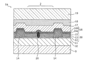
- FIG. 1 is a schematic cross-sectional view of a short-circuited organic EL element.
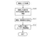
- FIG. 2 is a flowchart showing the steps in the method for producing an organic EL element of the present invention.
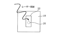
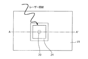
- FIG. 3A is a top view of the organic EL element for indicating the irradiation position of the laser.
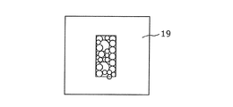
- FIG. 3B is a top view of the organic EL element for indicating the irradiation position of the laser.
- FIG. 4 is a schematic cross-sectional view showing a process of eliminating the short circuit of the organic EL element.
- FIG. 5 is a schematic cross-sectional view of the organic EL element in the first embodiment.
- FIG. 6 is a top view of the organic EL element for indicating the irradiation position of the laser.
- FIG. 1 is a schematic cross-sectional view of a short-circuited organic EL element.
- FIG. 2 is a flowchart showing the steps in the method for producing an organic EL element of the
- FIG. 7 is a schematic cross-sectional view showing a process of eliminating the short circuit of the organic EL element.
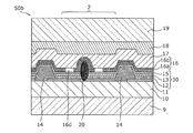
- FIG. 8 is a schematic cross-sectional view of the organic EL element in the second embodiment.
- FIG. 9 is a schematic cross-sectional view illustrating a process of eliminating the short circuit of the organic EL element in the second embodiment.
- FIG. 10 is a schematic cross-sectional view illustrating a process of eliminating the short circuit of the organic EL element in the third embodiment.
- FIG. 11 is a schematic cross-sectional view of the organic EL element in the third embodiment.
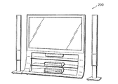
- FIG. 12 is an external view of a television system including the organic EL element of the present invention.
- the manufacturing method of the organic electroluminescent element concerning this invention is equipped with the lower electrode, the organic layer containing a light emitting layer, and an upper electrode, At least one of the said lower electrode and the said upper electrode is a transparent conductive material layer and the said transparent conductive material
- a femtosecond laser is irradiated to at least one of the transparent conductive material layer and the metal layer of the portion where the electrode is short-circuited and the periphery of the portion, and the structure of the transparent conductive material layer and the metal layer is determined.
- a second step of increasing resistance by changing is
- the light emitted from the organic EL element is refracted so as to be collected in the metal layer, it is possible to realize a strong cavity of the organic EL element. Further, by irradiating the ITO layer and the metal layer with laser light to increase the resistance, a short circuit between the lower electrode and the upper electrode can be reliably eliminated.
- the metal layer may be made of silver.
- the metal layer may be made of magnesium.
- the transparent conductive material layer may be made of a transparent metal oxide.
- the constituent material of the electrode is a transparent metal oxide
- the resistance can be increased by changing the tissue structure more reliably by irradiation with the femtosecond laser.
- the short-circuited portion may contain conductive foreign matter in the organic layer.
- the short circuit between the lower electrode and the upper electrode can be eliminated.
- the method may further include a step of detecting the conductive foreign matter, and the femtosecond laser may be irradiated to the transparent conductive material layer and the metal layer around the conductive foreign matter.
- the foreign object When a foreign object is irradiated with a laser, the foreign object absorbs the laser energy and vibrates, possibly causing damage to the pixels including the organic EL element.
- the position of the foreign object is detected and the laser around the foreign object is detected. Therefore, the short circuit can be eliminated without damaging the pixels.
- the thickness of the organic layer in the short-circuited portion may be smaller than the thickness of the organic layer other than the short-circuited portion.
- the lower electrode and the upper electrode are in direct contact due to the formation of the pinhole in the process of forming the organic EL element, or because the organic layer is thin, the lower electrode and the upper electrode are It is possible to eliminate a short circuit when the current is close and easy to flow.
- the organic electroluminescence device is an organic EL device including a lower electrode, an organic layer including a light emitting layer, and an upper electrode, wherein at least one of the lower electrode and the upper electrode is a transparent conductive material.
- the transparent conductive material layer and a part of the metal layer have a higher structure and a high resistance due to laser irradiation.
- the light emitted from the organic EL element is refracted so as to be collected in the metal layer, it is possible to realize a strong cavity of the organic EL element. Further, by irradiating the ITO layer and the metal layer with laser light to increase the resistance, a short circuit between the lower electrode and the upper electrode can be reliably eliminated.
- the metal layer may be made of silver.
- the metal layer may be made of magnesium.
- conductive foreign matter may be present in the vicinity of a part of the transparent conductive material layer and the metal layer.
- the organic EL element even if the organic EL element has a conductive foreign substance between the lower electrode and the upper electrode, the short circuit between the lower electrode and the upper electrode is eliminated, so that the organic EL element is used as an organic EL element. be able to.
- FIG. 1 is a schematic cross-sectional view of an organic EL element, showing a cross-sectional structure of a short-circuited organic EL element.
- the organic EL element 1a shown in the figure is an organic functional device having an organic layer including an anode, a cathode, and a light emitting layer sandwiched between the two electrodes.
- the organic EL element 1 a includes a planarizing film 10, an anode 11, a hole injection layer 12, a light emitting layer 13, a partition wall 14, and an electron injection layer 15 on a substrate 9.
- the cathode 16, the thin film sealing layer 17, the sealing resin layer 18, and the transparent glass 19 are provided.
- anode 11 and the cathode 16 correspond to the lower electrode and the upper electrode in the present invention, respectively.
- the hole injection layer 12, the light emitting layer 13, and the electron injection layer 15 correspond to the organic layers in the present invention.
- the substrate 9 is a substrate including, for example, a TFT (Thin Film Transistor).
- TFT Thin Film Transistor
- the planarization film 10 is made of an insulating organic material, for example, and is formed on a substrate including, for example, a driving thin film transistor (TFT).
- TFT driving thin film transistor
- the anode 11 is an anode to which holes are supplied, ie, an electric current flows from an external circuit.
- a reflective electrode made of Al or a silver alloy APC (silver-palladium-copper alloy) is formed on the planarizing film 10. It is the structure laminated
- the anode 11 may have a two-layer structure made of, for example, ITO (Indium Tin Oxide) and silver alloy APC.
- the hole injection layer 12 is a layer mainly composed of a hole injecting material.
- the hole injecting material is a material having a function of injecting holes injected from the anode 11 side into the light emitting layer 13 stably or by assisting the generation of holes.
- PEDOT polyethylene Compounds such as dioxythiophene
- aniline aniline
- the light emitting layer 13 is a layer that emits light when a voltage is applied between the anode 11 and the cathode 16.
- ⁇ -NPD Bis [N- (1-naphthyl) -N-phenyl] benzidine
- Alq 3 tris- (8-hydroxyquinoline) aluminum
- the thickness of the light emitting layer 13 is 20 nm or more and 70 nm or less as an example.
- the electron injection layer 15 is a layer mainly composed of an electron injecting material.
- the electron injecting material is a material having a function of injecting electrons injected from the cathode 16 into the light emitting layer 13 in a stable manner or assisting the generation of electrons.
- PPV polyphenylene vinylene
- the cathode 16 is a cathode to which electrons are supplied, that is, current flows out to an external circuit.
- the cathode 16 has a structure in which, for example, an ITO layer 16a and a metal layer 16b, which are transparent metal oxides, are laminated.
- the ITO layer 16a may be formed as a transparent electrode by using a material such as Mg or Ag.
- the metal layer 16b is formed of a material having a higher refractive index than the ITO layer 16a. Thereby, in the metal layer 16b, since the light radiate
- the metal layer 16b may be formed of a material such as silver (Ag), silver alloy APC, or magnesium (Mg).
- the thickness of the ITO layer 16a is 30 nm or more and 90 nm or less as an example, and the thickness of the metal layer 16b is 15 nm or more and 30 nm or less as an example.
- the partition wall 14 is a wall for separating the light emitting layer 13 into a plurality of light emitting regions, and is made of, for example, a photosensitive resin.
- the thin film sealing layer 17 is made of, for example, silicon nitride and has a function of blocking the light emitting layer 13 and the cathode 16 described above from water vapor and oxygen. This is to prevent the light emitting layer 13 itself or the cathode 16 from being deteriorated (oxidized) by being exposed to water vapor or oxygen.
- the sealing resin layer 18 is an acrylic or epoxy resin, and joins the transparent glass 19 and the layer integrally formed from the planarization film 10 to the thin film sealing layer 17 formed on the substrate described above. It has the function to do.
- the transparent glass 19 is a substrate that protects the light emitting surface of the light emitting panel, and is, for example, a transparent non-alkali glass having a thickness of 0.5 mm.
- the configuration of the anode 11, the light emitting layer 13, and the cathode 16 described above is a basic configuration of the organic EL element.
- the anode 11 side To holes and electrons from the cathode 16 side are respectively injected into the light emitting layer 13.
- the energy generated by recombination of these injected holes and electrons in the light emitting layer 13 the light emitting material of the light emitting layer 13 is excited and emits light.
- the material of the hole injection layer 12 and the electron injection layer 15 is not limited to this Embodiment, A well-known organic material or an inorganic material is used.
- the organic EL element 1a there may be a hole transport layer between the hole injection layer 12 and the light emitting layer 13, or an electron transport layer between the electron injection layer 15 and the light emitting layer 13. There may be.
- the hole transport layer is a layer mainly composed of a hole transport material.
- the hole transporting material has both the property of having an electron donor property and being easily converted to a cation (hole) and the property of transmitting the generated holes by intermolecular charge transfer reaction. It is a material that has suitability for up to charge transport.
- the electron transport layer is a layer mainly composed of an electron transport material.
- the electron transporting material has both the property of being an electron acceptor and easily becoming an anion, and the property of transmitting the generated electrons by a charge transfer reaction between molecules, and for charge transport from the cathode 16 to the light emitting layer 13. It is a material that has appropriateness to it.
- the organic EL element 1a may further include a color filter that adjusts red, green, and blue colors on the lower surface of the transparent glass 19 so as to cover each light emitting region separated by the partition wall 14. Good.
- the hole injection layer 12, the light emitting layer 13, and the electron injection layer 15 are collectively referred to as an organic layer 30.
- these layers are also included in the organic layer 30.
- the thickness of the organic layer 30 is 100 nm or more and 200 nm or less as an example.
- the planarization film 10, the anode 11, the organic layer 30, the cathode 16, the thin film sealing layer 17, the sealing resin layer 18, and the transparent glass 19 disposed in the light emitting region separated by the partition wall 14 are connected to the pixel 2. Called.
- the organic EL element 1 a shown in FIG. 1 in the manufacturing process, conductive foreign matter 20 is mixed between the anode 11 and the cathode 16, and the anode 11 and the cathode 16 are short-circuited via the foreign matter 20. Yes.
- the structure of the ITO layer 16a and the metal layer 16b constituting the part 16c of the cathode 16 above the position where the foreign substance 20 is mixed is changed to a laser 125. It is changed by irradiation to increase resistance. Thereby, the short circuit between the anode 11 and the cathode 16 short-circuited by the foreign material 20 is eliminated (repaired). The repair process for the short-circuited portion will be described later.
- a planarizing film 10 made of an insulating organic material is formed on a substrate 9 including a TFT, and then an anode 11 is formed on the planarizing film 10.
- the anode 11 is formed, for example, by depositing Al with a thickness of 30 nm on the planarizing film 10 by a sputtering method, and then performing a patterning process by photolithography and wet etching.
- the hole injection layer 12 is formed on the anode 11 by, for example, dissolving PEDOT in a solvent made of xylene and spin-coating this PEDOT solution.
- ⁇ -NPD and Alq 3 are stacked on the hole injection layer 12 by, for example, a vacuum deposition method, and the light emitting layer 13 is formed.
- the electron injection layer 15 is formed on the light-emitting layer 13 by, for example, dissolving polyphenylene vinylene (PPV) in a solvent made of, for example, xylene or chloroform and spin-coating it.
- PSV polyphenylene vinylene
- the ITO layer 16a is formed on the electron injection layer 15 without exposing the substrate on which the electron injection layer 15 is formed to the atmosphere. Specifically, 75 nm of ITO is laminated on the electron injection layer 15 by sputtering. At this time, the ITO layer 16a is in an amorphous state.
- the metal layer 16b is formed on the ITO layer 16a.
- a metal constituting the metal layer 16b for example, Ag, is deposited to a thickness of 20 nm on the ITO layer 16a by sputtering.
- the thickness of the metal layer 16b is increased, the light from the organic EL element is less likely to pass through the metal layer 16b, so that the display of the organic EL panel becomes darker.
- the viewing angle of the organic EL panel is narrowed by providing the metal layer 16b. That is, a stronger cavity can be achieved for the organic EL display device.
- the organic EL element 1a having a function as a light emitting element is formed by the manufacturing process as described above.
- the partition 14 which consists of surface photosensitive resin is formed in a predetermined position between the formation process of the anode 11, and the formation process of the positive hole injection layer 12.
- the thin film sealing layer 17 is formed on the metal layer 16b. Specifically, for example, 500 nm of silicon nitride is stacked on the metal layer 16b by a plasma CVD method. Since the thin film sealing layer 17 is formed in contact with the surface of the metal layer 16b, it is particularly preferable that the necessary conditions as a protective film are made strict.
- the material constituting the thin film sealing layer 17 is preferably a non-oxygen-based inorganic material typified by the aforementioned silicon nitride.
- an oxygen-based inorganic material such as silicon oxide (Si X O Y ) or silicon oxynitride (Si X O Y N Z ), or a structure in which a plurality of these inorganic materials are formed may be used.
- the forming method is not limited to the plasma CVD method, and may be other methods such as a sputtering method using argon plasma.
- a sealing resin layer 18 is applied to the surface of the thin film sealing layer 17. Thereafter, the transparent glass 19 is disposed on the applied sealing resin layer 18.
- the color filter is formed in advance on the main surface of the transparent glass 19. Thereafter, the transparent glass 19 is disposed on the applied sealing resin layer 18 with the surface on which the color filter is formed facing downward.
- the transparent glass 19 is pressed downward from the upper surface side, heat or energy rays are applied to cure the sealing resin layer 18, and the transparent glass 19 and the thin film sealing layer 17 are bonded.
- the organic EL element 1a is formed by such a forming method.
- the formation process of the anode 11, the hole injection layer 12, the light emitting layer 13, the electron injection layer 15, and the cathode 16 is not limited by this Embodiment.
- conductive foreign matter 20 is mixed between the anode 11 and the cathode 16, and the anode 11 and the cathode 16 are short-circuited via the foreign matter 20.
- the foreign material 20 for example, Al, which is a material of the anode 11, is deposited on the anode 11 after the formation of the anode 11, and then the hole injection layer 12, the light emitting layer 13, the electron injection layer 15, and the cathode 16 are laminated. It was because it was done.
- the size of the foreign material 20 is about 200 nm in diameter and about 500 nm in height. Since the anode 11 and the cathode 16 are short-circuited by the foreign matter 20, the organic EL element 1a does not emit light in this pixel 2, and becomes a dark spot pixel.
- FIG. 2 is a flowchart showing a process of eliminating the short circuit of the organic EL element 1a.
- Step S10 an organic EL element 1a having a short-circuited portion is prepared (step S10), a portion short-circuited by the foreign material 20 or the mixed foreign material 20 itself is detected (step S11), and short-circuited in the pixel 2.
- Laser irradiation is started from the transparent glass 19 side to the ITO layer 16a and the metal layer 16b of the cathode 16 above the portion (step S12). Thereby, a short circuit between the anode 11 and the cathode 16 is eliminated by changing a part of the structure of the cathode 16 irradiated with the laser to increase the resistance.
- Step S10 corresponds to the first step in the present invention
- step S12 corresponds to the second step in the present invention.
- a pixel in which the anode 11 and the cathode 16 are short-circuited or a foreign object 20 is detected by inputting a luminance signal voltage corresponding to the intermediate luminance gradation to each pixel 2 and emitting light at a lower luminance than that of a normal pixel. Is detected by a luminance measuring device or by visual observation.
- the detection of the short-circuited part or the foreign material 20 is not limited to the above-described method.
- the value of the current flowing between the anode 11 and the cathode 16 of the organic EL element is measured and detected based on the magnitude of the current value. May be.
- a forward bias voltage is applied, a current value equivalent to that of a normal pixel is obtained, and when a reverse bias voltage is applied, a portion where leakage light emission is observed is determined to be a short-circuited portion or a portion where foreign matter 20 is mixed. May be.
- FIG. 3A and 3B are top views of the organic EL element for showing a laser irradiation region on the foreign material 20
- FIG. 3A shows the organic EL element 1a before irradiation with the laser 125
- FIG. 3B shows irradiation with the laser 125.
- the top view of the subsequent organic EL element 1b is shown.
- 3A and 3B a region 22 surrounded by a solid line is a laser irradiation range.
- 4 and 5 are schematic cross-sectional views showing a process for eliminating the short circuit of the organic EL element.
- FIG. 4 shows the organic EL element 1a before irradiating the laser 125
- FIG. The cross-sectional schematic of this organic EL element 1b is shown.
- a laser 125 is irradiated on the cathode 16 in a region 22 of, for example, 5 ⁇ m ⁇ 10 ⁇ m around and around the portion where the anode 11 and the cathode 16 are short-circuited by the foreign matter 20.
- the type of the laser 125 to be irradiated for example, a femtosecond laser having an output energy of 1 ⁇ J to 30 ⁇ J and a pulse width of several hundred femtoseconds is used.
- the wavelength of the laser is 900 nm or more and 2500 nm or less.
- the focal point of the laser 125 is set according to the cathode 16.
- the focal point of the laser 125 is not limited to the cathode 16 but may be applied to the cathode 16 and the organic layer 30, or only one of the ITO layer 16 a or the metal layer 16 b of the cathode 16 may be applied. .
- the ITO layer 16a in an amorphous state is changed into a granular structure. Further, metal atoms constituting the metal layer 16b diffuse from the metal layer 16b to the ITO layer 16a. Accordingly, the region 22 of the organic EL element 1b after being irradiated with the laser 125 is in a state in which the granular structure of the ITO layer 16a and the metal atoms constituting the metal layer 16b are mixed.
- the granular texture structure means a texture structure in which a large number of particles are aggregated while leaving voids between the particles.
- the particle diameter of each particle constituting the granular structure is 10 nm or more and 500 nm or less.
- the shape of each particle may be spherical or flaky.
- the granular structure of the ITO layer 16a and metal atoms constituting the metal layer 16b are mixed, and voids are generated between the particles. Due to the voids, it is considered that a part of the cathode 16c having a granular texture structure is less resistant to current than the part of the cathode 16 having no granular structure, and has a high resistance.
- the resistance value (resistivity) of the cathode 16 in a portion having no granular structure is 50 ⁇ .
- the resistance value of the part 16d of the cathode having a granular structure is, for example, 40 M ⁇ .
- the region 22 of the organic EL element 1b after the laser 125 is irradiated is a granular shape of the ITO layer 16a.
- the organic material constituting the organic layer 30 is also mixed.
- the laser power may be, for example, a maximum value of 13 ⁇ W and a minimum value of 4 ⁇ W in the case of a laser with an oscillation frequency of 2 kHz.
- the maximum value of the laser power is an upper limit value for preventing the organic layer 30 disposed below the cathode 16 from being damaged.
- the minimum value of the laser power is a lower limit value of the laser power necessary for the constituent material of the cathode 16 to be granulated.
- the maximum value of 13 ⁇ W of laser power is 7.5 nJ when converted to laser output energy. Further, 4 ⁇ W, which is the minimum value of the laser power, is 2 nJ when converted to the output energy of the laser.
- the difference (power margin) between the maximum value and the minimum value of the laser power becomes large when the laser pulse width is 400 fs or more and 800 fs or less. Therefore, by irradiating the organic EL element 1a with a laser having a pulse width in this range by a femtosecond laser, the constituent material of the cathode 16 can be easily made into a granular structure.
- the thermal energy of the laser irradiated to the region 22 spreads in a range around the region 22, for example, about 1 ⁇ m away from the position irradiated with the laser, and the cathode 16 in this range is granulated to increase the resistance. There is also a case. Also in this case, the short circuit between the anode 11 and the cathode 16 is eliminated, and the light emission of the pixel 2 is restored.
- the cathode 16 is an organic EL element including an ITO layer and a metal layer in order to realize a strong cavity
- the ITO layer and the metal By irradiating the layer with laser light to increase the resistance, a short circuit between the anode and the cathode can be reliably eliminated.
- the output energy of the laser 125 is not limited to the above-described range, and any output energy may be used as long as the cathode 16 is granulated and the thin film sealing layer 17 is not destroyed.
- the irradiation of the laser 125 is not limited to the cathode 16 from the transparent glass 19 side.
- the focal position of the laser is adjusted and the anode 11 from the transparent glass 19 side is adjusted. You may go to Moreover, you may irradiate a laser from not only the transparent glass 19 side but the board
- FIG. 6 is a top view of the organic EL element for indicating the laser irradiation position.
- 7 and 8 are schematic cross-sectional views showing a process of eliminating the short circuit of the organic EL element.
- FIG. 7 shows the organic EL element 50a before irradiation with the laser 125
- FIG. 8 shows the organic after irradiation with the laser 125.
- the cross-sectional schematic of the EL element 50b is shown.
- a laser 125 is irradiated on the cathode 16 in a predetermined region around the foreign material 20.
- the surrounding ITO layer 16a and the metal layer 16b separated by about 10 ⁇ m from the foreign substance are irradiated with a laser in a square shape of a square of 20 ⁇ m ⁇ 20 ⁇ m.
- the structure of the part 16d of the cathode is granulated, and the short circuit between the anode 11 and the cathode 16 is eliminated.
- the foreign matter 20 absorbs the energy of the laser 125 and vibrates, which may cause damage to the pixels 2.
- the power of the laser 125 is increased or irradiation for a long time is required, so that the organic layer 30 may be damaged by heat.
- the focus of the laser 125 is set on the cathode 16 around the foreign material 20, so that the energy of the laser 125 can be prevented from being absorbed by the foreign material 20. Therefore, the structure of the cathode 16 around the foreign material 20 can be granulated without damaging the pixel 2 and the organic layer 30.
- the cathode 16 in a range surrounding the foreign material 20 is increased in resistance by being granulated. Thereby, the short circuit between the anode 11 and the cathode 16 is eliminated, and the light emission of the pixel 2 is recovered.
- the type, wavelength, and output energy of the laser 25 are the same as in the first embodiment described above, as long as the ITO layer 16a and the metal layer 16b have a high resistance and the thin film sealing layer 17 is not destroyed. You may change how. Further, similarly to the first embodiment, a step of detecting the position of the foreign matter 20 may be provided before the repair step.
- FIG. 10 is a schematic cross-sectional view showing a process of eliminating the short circuit of the organic EL element in the present embodiment.
- FIG. 11 is a schematic cross-sectional view of the organic EL element in the present embodiment. That is, FIG. 10 is a schematic cross-sectional view of the organic EL element 100a when the organic EL element 100a before repair is irradiated with the laser 125, and FIG. 11 is a schematic cross-sectional view of the organic EL element 100b after repair.
- the organic EL element 100a includes a planarizing film 110, an anode 111, and a hole injection layer 112 on a transparent glass 109, like the organic EL element 1a shown in the first embodiment.
- the cathode 16 has a structure in which, for example, an ITO layer 116a, which is a transparent metal oxide, and a metal layer 116b are laminated.
- the ITO layer 116a may be formed as a transparent electrode using a material such as Mg or Ag.
- the metal layer 116b may be a silver alloy APC.
- the thickness of the ITO layer 116a is, for example, 30 nm or more and 90 nm or less, and the thickness of the metal layer 116b is, for example, 15 nm or more and 30 nm or less.
- the hole injection layer 112, the light emitting layer 113, and the electron injection layer 115 are collectively referred to as an organic layer 130.
- these layers are also included in the organic layer 130.
- the planarization film 110, the anode 111, the organic layer 130, the cathode 116, the thin film sealing layer 117, the sealing resin layer 118, and the transparent glass 119 arranged in the light emitting region separated by the partition wall 114 are connected to the pixel 102. Called.
- the color filter is formed in advance on the main surface of the transparent glass 119. Thereafter, the transparent glass 119 is disposed on the applied sealing resin layer 118 with the surface on which the color filter is formed facing downward.
- the thin film sealing layer 117, the sealing resin layer 118, and the transparent glass 119 correspond to the protective film in the present invention.
- the anode 111 and the ITO layer 116 a of the cathode 116 are in direct contact with each other at the short-circuit portion 120.
- the ITO layer 116 a of the anode 111 and the cathode 116 is formed so that the thickness of the organic layer 130 of the short-circuit portion 120 is thinner than the thickness of the organic layer 130 other than the short-circuit portion 120.
- a pinhole is formed at the position of the short-circuited portion 120 in the formation process of the organic layer 130, and then the material constituting the ITO layer 116a is introduced into the pinhole in the formation process of the ITO layer 116a. Since 116a is formed, it is in direct contact as shown in FIG. Then, by increasing the resistance of the cathode part 116c, the short circuit between the shorted anode 111 and the ITO layer 116a is eliminated.
- Repair of the short-circuit portion 120 is performed by irradiating the laser 125 to the cathode 116 in the vicinity of the short-circuit portion 120 as in the first embodiment.
- the laser 125 is irradiated from the transparent glass 119 side to the ITO layer 116a and the metal layer 116b in the vicinity of the short-circuit portion 120.
- a part of the structure of the ITO layer 116a and the metal layer 116b is granulated.
- the granular structure of the ITO layer 116a and the metal constituting the metal layer 116b are mixed, and voids are generated between the particles. Therefore, it can be considered that due to the gap, a part of the granulated cathode 116c is less resistant to current than the non-granulated part of the cathode 116 and has a high resistance.
- the type of the laser 125 to be irradiated for example, a femtosecond laser having an output energy of 1 ⁇ J to 30 ⁇ J and a pulse width of several hundred femtoseconds is used.
- the wavelength of the laser is 900 nm or more and 2500 nm or less.
- the thermal energy of the laser spreads over a predetermined range around the region irradiated with the laser 125 in the organic EL element 100b.
- the cathode 116 in this range may be granulated to increase the resistance.
- the short circuit between the anode 111 and the cathode 116 is eliminated, and the light emission of the pixel 102 is restored.
- a step of detecting the short circuit portion 120 may be provided before the repair process of the short circuit portion 120.
- the size of the foreign material 20 is smaller than the distance between the anode 11 and the cathode 16, and the foreign material 20 is not electrically connected to the anode 11 and the cathode 16, but the foreign material 20 and the anode 11. Since the distance between the foreign material 20 and the cathode 16 is short, the resistance may be small and the current may flow easily.
- the short circuit between the anode 11 and the cathode 16 can be eliminated. That is, as in the first embodiment, by irradiating the laser 16 from the transparent glass 19 side to the cathode 16 above the portion where current easily flows, a part of the structure of the cathode 16 is granulated, It is possible to prevent a short circuit between the anode 11 and the cathode 16 by increasing the resistance of a part of the cathode 16.
- a pinhole is formed in the formation process of the light emitting layer 113 of the organic layer 130, and then, in the formation process of the cathode 116, a material constituting the cathode 116 is formed in the pinhole.
- the repair process described above can also be applied to the case where the cathode 116 is formed by flowing in, but the anode 111 and the cathode 116 are not completely conducted, but the distance between the anode 111 and the cathode 116 is short. It is also applicable to the case where the resistance is small and the current easily flows.
- the cathode 116 above the short-circuited portion is irradiated with the laser 125 from the transparent glass 119 side.
- the structure of the part 116c of the cathode 116 can be granulated. Thereby, a part of the cathode 116 can be increased in resistance, and a short circuit between the anode 111 and the cathode 116 can be prevented.
- the configuration in which the lower electrode is an anode and the upper electrode is a cathode is shown, but the lower electrode may be a cathode and the upper electrode may be an anode.
- the planarization film, anode, hole injection layer, light emitting layer, partition wall, electron injection layer, cathode, thin film sealing layer, sealing resin layer, and transparent glass, which are the constitution of the organic EL element, are as described above. Not only the configuration shown in the embodiment but also the material, configuration, and formation method may be changed.
- a hole transport layer may be provided between the hole injection layer and the light emitting layer, or an electron transport layer may be provided between the electron injection layer and the light emitting layer.
- separated by the partition may be covered may be sufficient.
- the laser irradiation position is not limited to the above-described embodiment, and may be set to a predetermined range including a foreign object or a short-circuit portion, or may be set only to the foreign object or the short-circuit portion. Moreover, you may set so that the circumference
- a thin flat television system 200 including the organic EL element according to the present invention as shown in FIG. 12 is also included in the present invention.
- the method for producing an organic EL element and the organic EL element according to the present invention are particularly useful in technical fields such as a flat-screen television and a display of a personal computer that require a large screen and high resolution.
Landscapes
- Engineering & Computer Science (AREA)
- Physics & Mathematics (AREA)
- Optics & Photonics (AREA)
- Mechanical Engineering (AREA)
- Plasma & Fusion (AREA)
- Manufacturing & Machinery (AREA)
- Chemical & Material Sciences (AREA)
- Chemical Kinetics & Catalysis (AREA)
- General Chemical & Material Sciences (AREA)
- Oil, Petroleum & Natural Gas (AREA)
- Multimedia (AREA)
- Signal Processing (AREA)
- Materials Engineering (AREA)
- Electroluminescent Light Sources (AREA)
Abstract
Description
以下に、本発明の実施の形態1について、図面を参照しながら説明する。
次に、実施の形態2について説明する。本実施の形態では、有機EL素子に照射されるレーザーの照射領域が実施の形態1と異なる。
次に、本発明の実施の形態3について説明する。本実施の形態が上述した実施の形態1と異なる点は、陽極と陰極が導電性異物を介さずに直接接触して短絡した有機EL素子において、短絡した部分のリペアを行う点である。
本発明のその他の実施の形態について説明する。上述した実施の形態は、陽極11と陰極16が完全に導通している場合だけではなく、陽極11と陰極16が完全に導通してはいないものの、他の部分と比べて陽極11と陰極16間の抵抗が小さい場合にも適用できる。
2、102 画素
11、111 陽極(下部電極)
12、112 正孔注入層(有機層)
13、113 発光層(有機層)
15、115 電子注入層(有機層)
16、116 陰極(上部電極)
16a、116a ITO層(透明導電性材料層)
16b、116b 金属層
16c、16d、116c 陰極の一部
20 異物
25、125 レーザー
30、130 有機層
120 短絡部分
200 薄型フラットテレビシステム
Claims (11)
- 下部電極、発光層を含む有機層および上部電極を備え、前記下部電極および前記上部電極の少なくとも一方は透明導電性材料層および前記透明導電性材料層より屈折率の高い金属層で構成され、前記下部電極と前記上部電極とが短絡している部分を有する有機エレクトロルミネッセンス(EL)素子を準備する第1の工程と、
前記下部電極と前記上部電極とが短絡している部分および当該部分の周囲のうち少なくとも一方の前記透明導電性材料層および前記金属層にフェムト秒レーザーを照射し、前記透明導電性材料層および前記金属層の組織構造を変化させて高抵抗化する第2の工程と、
を含む有機EL素子の製造方法。 - 前記金属層は、銀で構成されている、
請求項1に記載の有機EL素子の製造方法。 - 前記金属層は、マグネシウムで構成されている、
請求項1に記載の有機EL素子の製造方法。 - 前記透明導電性材料層は、透明金属酸化物で構成されている、
請求項1~3のいずれか1項に記載の有機EL素子の製造方法。 - 前記短絡している部分は、前記有機層に導電性の異物を含んでいる、
請求項1~4のいずれか1項に記載の有機EL素子の製造方法。 - 前記導電性の異物を検出する工程をさらに含み、
前記導電性の異物の周囲の前記透明導電性材料層および前記金属層に前記フェムト秒レーザーを照射する、
請求項5に記載の有機EL素子の製造方法。 - 前記短絡している部分の前記有機層の膜厚は、前記短絡している部分以外の前記有機層の膜厚より薄い、
請求項1~4のいずれか1項に記載の有機EL素子の製造方法。 - 下部電極、発光層を含む有機層および上部電極を備えた有機EL素子であって、
前記下部電極および前記上部電極の少なくとも一方は、透明導電性材料層および前記透明導電性材料層より屈折率の高い金属層で構成され、
前記透明導電性材料層および前記金属層の一部分は、レーザー照射により組織構造が変化し高抵抗化されている、
有機EL素子。 - 前記金属層は、銀で構成されている、
請求項8に記載の有機EL素子。 - 前記金属層は、マグネシウムで構成されている、
請求項8に記載の有機EL素子。 - 前記透明導電性材料層および前記金属層の一部分の近傍には、導電性の異物が存在する、
請求項8に記載の有機EL素子。
Priority Applications (2)
| Application Number | Priority Date | Filing Date | Title |
|---|---|---|---|
| JP2016559807A JP6388291B2 (ja) | 2014-11-17 | 2015-11-11 | 有機エレクトロルミネッセンス素子の製造方法および有機エレクトロルミネッセンス素子 |
| US15/527,491 US20170331041A1 (en) | 2014-11-17 | 2015-11-11 | Method for manufacturing organic electro-luminescent element and the organic electro-luminescent element |
Applications Claiming Priority (2)
| Application Number | Priority Date | Filing Date | Title |
|---|---|---|---|
| JP2014232871 | 2014-11-17 | ||
| JP2014-232871 | 2014-11-17 |
Publications (1)
| Publication Number | Publication Date |
|---|---|
| WO2016079957A1 true WO2016079957A1 (ja) | 2016-05-26 |
Family
ID=56013531
Family Applications (1)
| Application Number | Title | Priority Date | Filing Date |
|---|---|---|---|
| PCT/JP2015/005634 Ceased WO2016079957A1 (ja) | 2014-11-17 | 2015-11-11 | 有機エレクトロルミネッセンス素子の製造方法および有機エレクトロルミネッセンス素子 |
Country Status (3)
| Country | Link |
|---|---|
| US (1) | US20170331041A1 (ja) |
| JP (1) | JP6388291B2 (ja) |
| WO (1) | WO2016079957A1 (ja) |
Cited By (3)
| Publication number | Priority date | Publication date | Assignee | Title |
|---|---|---|---|---|
| WO2018216137A1 (ja) * | 2017-05-24 | 2018-11-29 | シャープ株式会社 | 表示デバイス、欠陥修正装置、製造装置、および欠陥修正方法 |
| JP2022076273A (ja) * | 2020-11-09 | 2022-05-19 | 株式会社Joled | 自発光型表示パネル、及び自発光型表示パネルの製造方法 |
| CN119407482A (zh) * | 2024-11-02 | 2025-02-11 | 北京工业大学 | 一种基于飞秒激光的镁电极表面加工方法 |
Families Citing this family (2)
| Publication number | Priority date | Publication date | Assignee | Title |
|---|---|---|---|---|
| JP6839581B2 (ja) * | 2016-04-01 | 2021-03-10 | 日東電工株式会社 | エレクトロクロミック調光部材、光透過性導電フィルムおよびエレクトロクロミック調光素子 |
| KR102826270B1 (ko) * | 2020-03-09 | 2025-06-27 | 삼성디스플레이 주식회사 | 표시 장치 및 표시 장치의 리페어 방법 |
Citations (10)
| Publication number | Priority date | Publication date | Assignee | Title |
|---|---|---|---|---|
| JP2001052878A (ja) * | 1999-08-11 | 2001-02-23 | Eastman Kodak Co | 透明カソード及びそれを含む有機発光ダイオード |
| JP2002208479A (ja) * | 2001-01-05 | 2002-07-26 | Toppan Printing Co Ltd | 有機led素子用中間抵抗膜付基板および有機led素子 |
| JP2008235177A (ja) * | 2007-03-23 | 2008-10-02 | Sharp Corp | 有機elディスプレイの製造方法及び有機elディスプレイ |
| JP2008235178A (ja) * | 2007-03-23 | 2008-10-02 | Sharp Corp | 有機elディスプレイの製造方法及び有機elディスプレイ |
| JP2012174334A (ja) * | 2011-02-17 | 2012-09-10 | Dainippon Printing Co Ltd | 有機elパネル及びその製造方法 |
| WO2012143974A1 (ja) * | 2011-04-20 | 2012-10-26 | パナソニック株式会社 | 有機エレクトロルミネッセンス素子の製造方法および有機エレクトロルミネッセンス素子 |
| JP2013114749A (ja) * | 2011-11-24 | 2013-06-10 | Panasonic Corp | 有機el素子の製造方法 |
| WO2013137403A1 (ja) * | 2012-03-14 | 2013-09-19 | 旭硝子株式会社 | 有機led素子、透光性基板、および透光性基板の製造方法 |
| JP2013197298A (ja) * | 2012-03-19 | 2013-09-30 | Panasonic Corp | 有機エレクトロルミネッセンス素子 |
| JP2015088319A (ja) * | 2013-10-30 | 2015-05-07 | ソニー株式会社 | 表示装置および電子機器 |
Family Cites Families (5)
| Publication number | Priority date | Publication date | Assignee | Title |
|---|---|---|---|---|
| US6909111B2 (en) * | 2000-12-28 | 2005-06-21 | Semiconductor Energy Laboratory Co., Ltd. | Method of manufacturing a light emitting device and thin film forming apparatus |
| EP1794255B1 (en) * | 2004-08-19 | 2016-11-16 | LG Chem, Ltd. | Organic light-emitting device comprising buffer layer and method for fabricating the same |
| JP2006221982A (ja) * | 2005-02-10 | 2006-08-24 | Toshiba Matsushita Display Technology Co Ltd | アレイ基板の製造方法及び有機el表示装置の製造方法 |
| JP5760009B2 (ja) * | 2010-12-01 | 2015-08-05 | 株式会社Joled | 有機エレクトロルミネッセンス素子の製造方法 |
| WO2012172612A1 (ja) * | 2011-06-16 | 2012-12-20 | パナソニック株式会社 | 有機エレクトロルミネッセンス素子の製造方法および有機エレクトロルミネッセンス素子 |
-
2015
- 2015-11-11 WO PCT/JP2015/005634 patent/WO2016079957A1/ja not_active Ceased
- 2015-11-11 JP JP2016559807A patent/JP6388291B2/ja active Active
- 2015-11-11 US US15/527,491 patent/US20170331041A1/en not_active Abandoned
Patent Citations (10)
| Publication number | Priority date | Publication date | Assignee | Title |
|---|---|---|---|---|
| JP2001052878A (ja) * | 1999-08-11 | 2001-02-23 | Eastman Kodak Co | 透明カソード及びそれを含む有機発光ダイオード |
| JP2002208479A (ja) * | 2001-01-05 | 2002-07-26 | Toppan Printing Co Ltd | 有機led素子用中間抵抗膜付基板および有機led素子 |
| JP2008235177A (ja) * | 2007-03-23 | 2008-10-02 | Sharp Corp | 有機elディスプレイの製造方法及び有機elディスプレイ |
| JP2008235178A (ja) * | 2007-03-23 | 2008-10-02 | Sharp Corp | 有機elディスプレイの製造方法及び有機elディスプレイ |
| JP2012174334A (ja) * | 2011-02-17 | 2012-09-10 | Dainippon Printing Co Ltd | 有機elパネル及びその製造方法 |
| WO2012143974A1 (ja) * | 2011-04-20 | 2012-10-26 | パナソニック株式会社 | 有機エレクトロルミネッセンス素子の製造方法および有機エレクトロルミネッセンス素子 |
| JP2013114749A (ja) * | 2011-11-24 | 2013-06-10 | Panasonic Corp | 有機el素子の製造方法 |
| WO2013137403A1 (ja) * | 2012-03-14 | 2013-09-19 | 旭硝子株式会社 | 有機led素子、透光性基板、および透光性基板の製造方法 |
| JP2013197298A (ja) * | 2012-03-19 | 2013-09-30 | Panasonic Corp | 有機エレクトロルミネッセンス素子 |
| JP2015088319A (ja) * | 2013-10-30 | 2015-05-07 | ソニー株式会社 | 表示装置および電子機器 |
Cited By (3)
| Publication number | Priority date | Publication date | Assignee | Title |
|---|---|---|---|---|
| WO2018216137A1 (ja) * | 2017-05-24 | 2018-11-29 | シャープ株式会社 | 表示デバイス、欠陥修正装置、製造装置、および欠陥修正方法 |
| JP2022076273A (ja) * | 2020-11-09 | 2022-05-19 | 株式会社Joled | 自発光型表示パネル、及び自発光型表示パネルの製造方法 |
| CN119407482A (zh) * | 2024-11-02 | 2025-02-11 | 北京工业大学 | 一种基于飞秒激光的镁电极表面加工方法 |
Also Published As
| Publication number | Publication date |
|---|---|
| JP6388291B2 (ja) | 2018-09-12 |
| US20170331041A1 (en) | 2017-11-16 |
| JPWO2016079957A1 (ja) | 2017-07-13 |
Similar Documents
| Publication | Publication Date | Title |
|---|---|---|
| JP5760009B2 (ja) | 有機エレクトロルミネッセンス素子の製造方法 | |
| JP5642277B2 (ja) | 有機エレクトロルミネッセンス素子の製造方法および有機エレクトロルミネッセンス素子 | |
| JP5805181B2 (ja) | 有機エレクトロルミネッセンス素子の製造方法 | |
| JP6405560B2 (ja) | 表示パネルの製造方法 | |
| JP6388291B2 (ja) | 有機エレクトロルミネッセンス素子の製造方法および有機エレクトロルミネッセンス素子 | |
| JP5654037B2 (ja) | 有機el素子の製造方法及び評価方法 | |
| JP6086333B2 (ja) | 有機エレクトロルミネッセンス表示装置の製造方法および有機エレクトロルミネッセンス表示装置 | |
| JP5657123B2 (ja) | 有機elパネルおよびその製造方法 | |
| JP5687339B2 (ja) | 有機el素子及び有機el素子の製造方法 | |
| JP6057143B2 (ja) | 有機エレクトロルミネッセンス素子 | |
| JP2013114749A (ja) | 有機el素子の製造方法 | |
| JP6563311B2 (ja) | 表示パネルの製造方法および表示パネル | |
| JP6041087B2 (ja) | 表示パネルの製造方法、その検査装置及び検査方法 | |
| JP2011124152A (ja) | 有機エレクトロルミネッセンス表示装置の製造方法および有機エレクトロルミネッセンス表示装置 | |
| JP6561290B2 (ja) | 表示パネルの製造方法および表示パネル | |
| JP5938692B2 (ja) | 表示パネルの製造方法、その検査装置及び検査方法 | |
| JP6040553B2 (ja) | 発光デバイス、発光デバイスの製造方法及び電子機器 | |
| WO2015111119A1 (ja) | 表示装置の製造方法および表示装置 |
Legal Events
| Date | Code | Title | Description |
|---|---|---|---|
| 121 | Ep: the epo has been informed by wipo that ep was designated in this application |
Ref document number: 15861615 Country of ref document: EP Kind code of ref document: A1 |
|
| ENP | Entry into the national phase |
Ref document number: 2016559807 Country of ref document: JP Kind code of ref document: A |
|
| NENP | Non-entry into the national phase |
Ref country code: DE |
|
| WWE | Wipo information: entry into national phase |
Ref document number: 15527491 Country of ref document: US |
|
| 122 | Ep: pct application non-entry in european phase |
Ref document number: 15861615 Country of ref document: EP Kind code of ref document: A1 |