WO2016056409A1 - 積層型デバイスおよび製造方法、並びに、電子機器 - Google Patents
積層型デバイスおよび製造方法、並びに、電子機器 Download PDFInfo
- Publication number
- WO2016056409A1 WO2016056409A1 PCT/JP2015/077241 JP2015077241W WO2016056409A1 WO 2016056409 A1 WO2016056409 A1 WO 2016056409A1 JP 2015077241 W JP2015077241 W JP 2015077241W WO 2016056409 A1 WO2016056409 A1 WO 2016056409A1
- Authority
- WO
- WIPO (PCT)
- Prior art keywords
- substrate
- metal layer
- bonding pad
- bonding
- multilayer device
- Prior art date
- Legal status (The legal status is an assumption and is not a legal conclusion. Google has not performed a legal analysis and makes no representation as to the accuracy of the status listed.)
- Ceased
Links
Images





Classifications
-
- H—ELECTRICITY
- H10—SEMICONDUCTOR DEVICES; ELECTRIC SOLID-STATE DEVICES NOT OTHERWISE PROVIDED FOR
- H10W—GENERIC PACKAGES, INTERCONNECTIONS, CONNECTORS OR OTHER CONSTRUCTIONAL DETAILS OF DEVICES COVERED BY CLASS H10
- H10W20/00—Interconnections in chips, wafers or substrates
- H10W20/40—Interconnections external to wafers or substrates, e.g. back-end-of-line [BEOL] metallisations or vias connecting to gate electrodes
- H10W20/41—Interconnections external to wafers or substrates, e.g. back-end-of-line [BEOL] metallisations or vias connecting to gate electrodes characterised by their conductive parts
- H10W20/423—Shielding layers
-
- H—ELECTRICITY
- H10—SEMICONDUCTOR DEVICES; ELECTRIC SOLID-STATE DEVICES NOT OTHERWISE PROVIDED FOR
- H10F—INORGANIC SEMICONDUCTOR DEVICES SENSITIVE TO INFRARED RADIATION, LIGHT, ELECTROMAGNETIC RADIATION OF SHORTER WAVELENGTH OR CORPUSCULAR RADIATION
- H10F39/00—Integrated devices, or assemblies of multiple devices, comprising at least one element covered by group H10F30/00, e.g. radiation detectors comprising photodiode arrays
- H10F39/80—Constructional details of image sensors
- H10F39/811—Interconnections
-
- H—ELECTRICITY
- H04—ELECTRIC COMMUNICATION TECHNIQUE
- H04N—PICTORIAL COMMUNICATION, e.g. TELEVISION
- H04N25/00—Circuitry of solid-state image sensors [SSIS]; Control thereof
- H04N25/60—Noise processing, e.g. detecting, correcting, reducing or removing noise
-
- H—ELECTRICITY
- H04—ELECTRIC COMMUNICATION TECHNIQUE
- H04N—PICTORIAL COMMUNICATION, e.g. TELEVISION
- H04N25/00—Circuitry of solid-state image sensors [SSIS]; Control thereof
- H04N25/70—SSIS architectures; Circuits associated therewith
-
- H—ELECTRICITY
- H10—SEMICONDUCTOR DEVICES; ELECTRIC SOLID-STATE DEVICES NOT OTHERWISE PROVIDED FOR
- H10F—INORGANIC SEMICONDUCTOR DEVICES SENSITIVE TO INFRARED RADIATION, LIGHT, ELECTROMAGNETIC RADIATION OF SHORTER WAVELENGTH OR CORPUSCULAR RADIATION
- H10F39/00—Integrated devices, or assemblies of multiple devices, comprising at least one element covered by group H10F30/00, e.g. radiation detectors comprising photodiode arrays
- H10F39/011—Manufacture or treatment of image sensors covered by group H10F39/12
- H10F39/018—Manufacture or treatment of image sensors covered by group H10F39/12 of hybrid image sensors
-
- H—ELECTRICITY
- H10—SEMICONDUCTOR DEVICES; ELECTRIC SOLID-STATE DEVICES NOT OTHERWISE PROVIDED FOR
- H10F—INORGANIC SEMICONDUCTOR DEVICES SENSITIVE TO INFRARED RADIATION, LIGHT, ELECTROMAGNETIC RADIATION OF SHORTER WAVELENGTH OR CORPUSCULAR RADIATION
- H10F39/00—Integrated devices, or assemblies of multiple devices, comprising at least one element covered by group H10F30/00, e.g. radiation detectors comprising photodiode arrays
- H10F39/80—Constructional details of image sensors
-
- H—ELECTRICITY
- H10—SEMICONDUCTOR DEVICES; ELECTRIC SOLID-STATE DEVICES NOT OTHERWISE PROVIDED FOR
- H10F—INORGANIC SEMICONDUCTOR DEVICES SENSITIVE TO INFRARED RADIATION, LIGHT, ELECTROMAGNETIC RADIATION OF SHORTER WAVELENGTH OR CORPUSCULAR RADIATION
- H10F39/00—Integrated devices, or assemblies of multiple devices, comprising at least one element covered by group H10F30/00, e.g. radiation detectors comprising photodiode arrays
- H10F39/80—Constructional details of image sensors
- H10F39/805—Coatings
-
- H—ELECTRICITY
- H10—SEMICONDUCTOR DEVICES; ELECTRIC SOLID-STATE DEVICES NOT OTHERWISE PROVIDED FOR
- H10F—INORGANIC SEMICONDUCTOR DEVICES SENSITIVE TO INFRARED RADIATION, LIGHT, ELECTROMAGNETIC RADIATION OF SHORTER WAVELENGTH OR CORPUSCULAR RADIATION
- H10F39/00—Integrated devices, or assemblies of multiple devices, comprising at least one element covered by group H10F30/00, e.g. radiation detectors comprising photodiode arrays
- H10F39/80—Constructional details of image sensors
- H10F39/805—Coatings
- H10F39/8057—Optical shielding
-
- H—ELECTRICITY
- H10—SEMICONDUCTOR DEVICES; ELECTRIC SOLID-STATE DEVICES NOT OTHERWISE PROVIDED FOR
- H10F—INORGANIC SEMICONDUCTOR DEVICES SENSITIVE TO INFRARED RADIATION, LIGHT, ELECTROMAGNETIC RADIATION OF SHORTER WAVELENGTH OR CORPUSCULAR RADIATION
- H10F39/00—Integrated devices, or assemblies of multiple devices, comprising at least one element covered by group H10F30/00, e.g. radiation detectors comprising photodiode arrays
- H10F39/80—Constructional details of image sensors
- H10F39/809—Constructional details of image sensors of hybrid image sensors
-
- H—ELECTRICITY
- H10—SEMICONDUCTOR DEVICES; ELECTRIC SOLID-STATE DEVICES NOT OTHERWISE PROVIDED FOR
- H10P—GENERIC PROCESSES OR APPARATUS FOR THE MANUFACTURE OR TREATMENT OF DEVICES COVERED BY CLASS H10
- H10P14/00—Formation of materials, e.g. in the shape of layers or pillars
- H10P14/40—Formation of materials, e.g. in the shape of layers or pillars of conductive or resistive materials
-
- H—ELECTRICITY
- H10—SEMICONDUCTOR DEVICES; ELECTRIC SOLID-STATE DEVICES NOT OTHERWISE PROVIDED FOR
- H10W—GENERIC PACKAGES, INTERCONNECTIONS, CONNECTORS OR OTHER CONSTRUCTIONAL DETAILS OF DEVICES COVERED BY CLASS H10
- H10W20/00—Interconnections in chips, wafers or substrates
- H10W20/01—Manufacture or treatment
-
- H—ELECTRICITY
- H10—SEMICONDUCTOR DEVICES; ELECTRIC SOLID-STATE DEVICES NOT OTHERWISE PROVIDED FOR
- H10W—GENERIC PACKAGES, INTERCONNECTIONS, CONNECTORS OR OTHER CONSTRUCTIONAL DETAILS OF DEVICES COVERED BY CLASS H10
- H10W20/00—Interconnections in chips, wafers or substrates
- H10W20/40—Interconnections external to wafers or substrates, e.g. back-end-of-line [BEOL] metallisations or vias connecting to gate electrodes
-
- H—ELECTRICITY
- H10—SEMICONDUCTOR DEVICES; ELECTRIC SOLID-STATE DEVICES NOT OTHERWISE PROVIDED FOR
- H10W—GENERIC PACKAGES, INTERCONNECTIONS, CONNECTORS OR OTHER CONSTRUCTIONAL DETAILS OF DEVICES COVERED BY CLASS H10
- H10W20/00—Interconnections in chips, wafers or substrates
- H10W20/40—Interconnections external to wafers or substrates, e.g. back-end-of-line [BEOL] metallisations or vias connecting to gate electrodes
- H10W20/41—Interconnections external to wafers or substrates, e.g. back-end-of-line [BEOL] metallisations or vias connecting to gate electrodes characterised by their conductive parts
- H10W20/42—Vias, e.g. via plugs
-
- H—ELECTRICITY
- H10—SEMICONDUCTOR DEVICES; ELECTRIC SOLID-STATE DEVICES NOT OTHERWISE PROVIDED FOR
- H10W—GENERIC PACKAGES, INTERCONNECTIONS, CONNECTORS OR OTHER CONSTRUCTIONAL DETAILS OF DEVICES COVERED BY CLASS H10
- H10W20/00—Interconnections in chips, wafers or substrates
- H10W20/40—Interconnections external to wafers or substrates, e.g. back-end-of-line [BEOL] metallisations or vias connecting to gate electrodes
- H10W20/41—Interconnections external to wafers or substrates, e.g. back-end-of-line [BEOL] metallisations or vias connecting to gate electrodes characterised by their conductive parts
- H10W20/427—Power or ground buses
-
- H—ELECTRICITY
- H10—SEMICONDUCTOR DEVICES; ELECTRIC SOLID-STATE DEVICES NOT OTHERWISE PROVIDED FOR
- H10W—GENERIC PACKAGES, INTERCONNECTIONS, CONNECTORS OR OTHER CONSTRUCTIONAL DETAILS OF DEVICES COVERED BY CLASS H10
- H10W70/00—Package substrates; Interposers; Redistribution layers [RDL]
- H10W70/01—Manufacture or treatment
- H10W70/05—Manufacture or treatment of insulating or insulated package substrates, or of interposers, or of redistribution layers
- H10W70/093—Connecting or disconnecting other interconnections thereto or therefrom, e.g. connecting bond wires or bumps
-
- H—ELECTRICITY
- H10—SEMICONDUCTOR DEVICES; ELECTRIC SOLID-STATE DEVICES NOT OTHERWISE PROVIDED FOR
- H10W—GENERIC PACKAGES, INTERCONNECTIONS, CONNECTORS OR OTHER CONSTRUCTIONAL DETAILS OF DEVICES COVERED BY CLASS H10
- H10W70/00—Package substrates; Interposers; Redistribution layers [RDL]
- H10W70/01—Manufacture or treatment
- H10W70/05—Manufacture or treatment of insulating or insulated package substrates, or of interposers, or of redistribution layers
- H10W70/095—Manufacture or treatment of insulating or insulated package substrates, or of interposers, or of redistribution layers of vias therein
-
- H—ELECTRICITY
- H10—SEMICONDUCTOR DEVICES; ELECTRIC SOLID-STATE DEVICES NOT OTHERWISE PROVIDED FOR
- H10W—GENERIC PACKAGES, INTERCONNECTIONS, CONNECTORS OR OTHER CONSTRUCTIONAL DETAILS OF DEVICES COVERED BY CLASS H10
- H10W70/00—Package substrates; Interposers; Redistribution layers [RDL]
- H10W70/60—Insulating or insulated package substrates; Interposers; Redistribution layers
-
- H—ELECTRICITY
- H10—SEMICONDUCTOR DEVICES; ELECTRIC SOLID-STATE DEVICES NOT OTHERWISE PROVIDED FOR
- H10W—GENERIC PACKAGES, INTERCONNECTIONS, CONNECTORS OR OTHER CONSTRUCTIONAL DETAILS OF DEVICES COVERED BY CLASS H10
- H10W70/00—Package substrates; Interposers; Redistribution layers [RDL]
- H10W70/60—Insulating or insulated package substrates; Interposers; Redistribution layers
- H10W70/611—Insulating or insulated package substrates; Interposers; Redistribution layers for connecting multiple chips together
-
- H—ELECTRICITY
- H10—SEMICONDUCTOR DEVICES; ELECTRIC SOLID-STATE DEVICES NOT OTHERWISE PROVIDED FOR
- H10W—GENERIC PACKAGES, INTERCONNECTIONS, CONNECTORS OR OTHER CONSTRUCTIONAL DETAILS OF DEVICES COVERED BY CLASS H10
- H10W99/00—Subject matter not provided for in other groups of this subclass
-
- H—ELECTRICITY
- H10—SEMICONDUCTOR DEVICES; ELECTRIC SOLID-STATE DEVICES NOT OTHERWISE PROVIDED FOR
- H10D—INORGANIC ELECTRIC SEMICONDUCTOR DEVICES
- H10D89/00—Aspects of integrated devices not covered by groups H10D84/00 - H10D88/00
- H10D89/10—Integrated device layouts
-
- H—ELECTRICITY
- H10—SEMICONDUCTOR DEVICES; ELECTRIC SOLID-STATE DEVICES NOT OTHERWISE PROVIDED FOR
- H10W—GENERIC PACKAGES, INTERCONNECTIONS, CONNECTORS OR OTHER CONSTRUCTIONAL DETAILS OF DEVICES COVERED BY CLASS H10
- H10W42/00—Arrangements for protection of devices
- H10W42/20—Arrangements for protection of devices protecting against electromagnetic or particle radiation, e.g. light, X-rays, gamma-rays or electrons
- H10W42/261—Arrangements for protection of devices protecting against electromagnetic or particle radiation, e.g. light, X-rays, gamma-rays or electrons characterised by their shapes or dispositions
- H10W42/271—Arrangements for protection of devices protecting against electromagnetic or particle radiation, e.g. light, X-rays, gamma-rays or electrons characterised by their shapes or dispositions the arrangements being between stacked chips
-
- H—ELECTRICITY
- H10—SEMICONDUCTOR DEVICES; ELECTRIC SOLID-STATE DEVICES NOT OTHERWISE PROVIDED FOR
- H10W—GENERIC PACKAGES, INTERCONNECTIONS, CONNECTORS OR OTHER CONSTRUCTIONAL DETAILS OF DEVICES COVERED BY CLASS H10
- H10W70/00—Package substrates; Interposers; Redistribution layers [RDL]
- H10W70/01—Manufacture or treatment
- H10W70/05—Manufacture or treatment of insulating or insulated package substrates, or of interposers, or of redistribution layers
-
- H—ELECTRICITY
- H10—SEMICONDUCTOR DEVICES; ELECTRIC SOLID-STATE DEVICES NOT OTHERWISE PROVIDED FOR
- H10W—GENERIC PACKAGES, INTERCONNECTIONS, CONNECTORS OR OTHER CONSTRUCTIONAL DETAILS OF DEVICES COVERED BY CLASS H10
- H10W70/00—Package substrates; Interposers; Redistribution layers [RDL]
- H10W70/60—Insulating or insulated package substrates; Interposers; Redistribution layers
- H10W70/67—Insulating or insulated package substrates; Interposers; Redistribution layers characterised by their insulating layers or insulating parts
- H10W70/68—Shapes or dispositions thereof
- H10W70/685—Shapes or dispositions thereof comprising multiple insulating layers
Definitions
- the present disclosure relates to a multilayer device, a manufacturing method, and an electronic apparatus, and more particularly, to a multilayer device and a manufacturing method capable of suppressing adverse effects of noise generated from one substrate on the other substrate, and And electronic devices.
- a solid-state imaging device such as a CCD (Charge Coupled Device) or a CMOS (Complementary Metal Oxide Semiconductor) image sensor is used.
- CCD Charge Coupled Device
- CMOS Complementary Metal Oxide Semiconductor
- Patent Documents 1 and 2 a technique for manufacturing a solid-state imaging device using a stacked device in which a plurality of substrates are stacked has been developed.
- a plurality of dummy patterns made of metal are arranged in a staggered pattern on the joint surface, and the bonding surface is all viewed from above or below.
- a technique for forming a light-shielding layer with a metal structure is disclosed.
- noise due to electromagnetic waves generated when one of the substrates operates may have an adverse effect such as causing malfunction in the other substrate.
- it is required to provide a structure for blocking electromagnetic waves between the substrates.
- the metal structure in the multilayer device disclosed in Patent Document 3 described above is intended to shield light, and thus the dummy pattern disposed on the bonding surface is electrically floating (floating). It was not possible to block such electromagnetic waves.
- the present disclosure has been made in view of such a situation, and is intended to suppress adverse effects of noise generated from one substrate on the other substrate.
- a stacked device includes a first metal layer formed on one of a plurality of substrates stacked in at least two layers, and the other stacked on the one substrate.
- a second metal layer formed on the first substrate and bonding the first metal layer and the second metal layer to fix the potential between the one substrate and the other substrate.
- An electromagnetic wave shielding structure for blocking electromagnetic waves between them is formed.
- a method for manufacturing a stacked device in which a first metal layer is formed on one of a plurality of substrates stacked in at least two layers and stacked on the one substrate. Forming a second metal layer on the other substrate, bonding the first metal layer and the second metal layer, and fixing the potential between the one substrate and the other substrate. And forming an electromagnetic wave shielding structure for shielding electromagnetic waves.
- An electronic device includes a first metal layer formed on one of a plurality of substrates stacked in at least two layers, and the other stacked on the one substrate.
- a second metal layer formed on the substrate, and bonding the first metal layer and the second metal layer to fix the potential between the one substrate and the other substrate.
- a multilayer device that constitutes an electromagnetic wave shielding structure that shields electromagnetic waves between them is provided.
- a first metal layer is formed on one of a plurality of substrates stacked in at least two layers, and the first substrate is stacked on the other substrate. Two metal layers are formed.
- substrate is comprised by joining and fixing the electric potential of the metal layer of one board
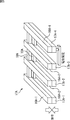
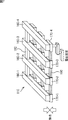
- FIG. 1 is a diagram illustrating a configuration example of a first embodiment of a stacked device to which the present technology is applied.
- FIG. 1 schematically shows a structure in which the multilayer device 11 is viewed from an oblique direction, and the multilayer device 11 is configured by laminating an upper substrate 12 and a lower substrate 13.
- a solid-state imaging device such as a CMOS image sensor can be configured by the stacked device 11.
- the upper substrate 12 is a sensor substrate on which photodiodes and a plurality of transistors constituting pixels are formed
- the lower substrate 13 is formed with a drive circuit, a control circuit, and the like that drive the pixels.
- Peripheral circuit board Peripheral circuit board.
- the upper substrate 12 and the lower substrate 13 are individually formed. Then, the bonding surface 14 (the surface facing downward in FIG. 1) of the upper substrate 12 and the bonding surface 15 (the surface facing upward in FIG. 1) of the lower substrate 13 are bonded and bonded to each other. As shown on the lower side, the integrated multilayer device 11 is formed.
- a metal layer on which a plurality of bonding pads 16 are formed is provided so as to be exposed on the bonding surface 14 of the upper substrate 12, and a plurality of bonding pads 17 are formed so as to be exposed on the bonding surface 15 of the lower substrate 13.
- a metal layer is provided.
- the bonding pad 16 and the bonding pad 17 are made of, for example, a metal having conductivity, and are connected to elements (not shown) provided on the upper substrate 12 and the lower substrate 13 respectively.
- the plurality of bonding pads 16 of the upper substrate 12 and the plurality of bonding pads 17 of the lower substrate 13 are formed at positions corresponding to each other when the upper substrate 12 and the lower substrate 13 are bonded. . Therefore, in the multilayer device 11, the upper substrate 12 and the lower substrate 13 are bonded by metal bonding the bonding pad 16 and the bonding pad 17 over the entire surface.
- the plurality of bonding pads 16 of the upper substrate 12 are independently arranged at a predetermined interval
- the plurality of bonding pads 17 of the lower substrate 13 are independently arranged at a predetermined interval.
- the bonding pad 16 and the bonding pad 17 are formed in a rectangular shape having a side length of 0.1 to 100 ⁇ m, and are arranged in a pattern such that the interval is 0.005 ⁇ m to 1000 ⁇ m.
- the bonding pad 16 and the bonding pad 17 may have a round shape instead of a rectangular shape.
- adjacent bonding pads 16 are connected by a connection wiring 18 formed in the same layer as the bonding pad 16.
- adjacent bonding pads 17 are connected to the bonding pad 17. They are connected by a connecting wire 19 formed in the same layer.
- at least one of the plurality of bonding pads 16 and bonding pads 17 is connected to a circuit that is electrically fixed. For example, in the configuration example of FIG. 1, one of the bonding pads 17 of the lower substrate 13 is fixed in potential.
- the multilayer device 11 configured as described above has an electromagnetic wave shield configuration configured by bonding the bonding pad 16 and the bonding pad 17 to fix the potential, thereby preventing electromagnetic waves between the upper substrate 12 and the lower substrate 13. Can be blocked. Therefore, for example, noise due to electromagnetic waves generated during operation of the upper substrate 12 can be prevented from adversely affecting the lower substrate 13 such as malfunction. Similarly, noise due to electromagnetic waves generated during operation of the lower substrate 13 can be prevented from adversely affecting the upper substrate 12 such as malfunction.
- the electromagnetic wave shielding configuration constituted by the bonding pad 16 and the bonding pad 17 can be provided on the entire surface of the multilayer device 11, for example.
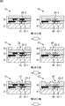
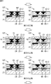
- the multilayer device 11 Next, a manufacturing method of the multilayer device 11 will be described with reference to FIGS. As described above, after the upper substrate 12 and the lower substrate 13 are formed separately, the upper substrate 12 and the lower substrate 13 are stacked to manufacture the stacked device 11.
- the upper substrate 12 is formed with the wiring layer 22 so as to be laminated on the silicon substrate 21, and the lower substrate 13 is laminated on the silicon substrate 41.
- a wiring layer 42 is formed on the substrate.
- the wiring layer 22 of the upper substrate 12 has a multilayer wiring structure in which a plurality of wirings are formed in an interlayer insulating film.
- the wiring 23-1 is connected to the silicon substrate 21 by the connection electrode 24.
- the wiring layer 42 of the lower substrate 13 has a two-layer wiring structure including a lower wiring 43-1 and an upper wiring 43-2, and the wiring 43-1 is connected to the silicon substrate 41 by the connection electrode 44. It is connected to the.
- interlayer insulating films constituting the wiring layer 22 and the wiring layer 42 include SiO2 (silicon dioxide), SiN (silicon nitride), SiOCH (carbon-containing silicon oxide), SiCN (carbon-containing silicon nitride). Such a composition is adopted. Further, Cu (copper) wiring is adopted for the wirings 23-1 and 23-2 of the wiring layer 22 and the wiring 43-1 of the wiring layer 42, and Al (aluminum) is used for the wiring 43-2 of the wiring layer 42. ) Wiring is adopted. A method for forming such a wiring is already known, for example, by “Full-Copper-Wiring-in-a-Sub-0.25um CMOS-ULSI Technology,” Proc.
- the opening 26 is opened in the resist 25 by a general lithography technique.
- an opening 46 is opened in the resist 45 after the resist 45 is applied to the wiring layer 42.
- the resist 25 and the resist 45 are formed, for example, in a thickness range of 0.05 to 5 ⁇ m.
- ArF fluorine fluoride argon
- KrF krypton difluoride
- a cleaning process is performed.
- a trench 27 for forming the bonding pad 16 is formed in the upper substrate 12, and a trench 47 for forming the bonding pad 17 is formed in the lower substrate 13.
- the upper substrate 12 is formed smaller than the trench 27 by a general lithography technique after the resist 28 is applied to the wiring layer 22.
- an opening 29 is opened in the resist 28.
- an opening 49 is opened in the resist 48 so as to be formed smaller than the trench 47.
- a cleaning process is performed.
- a trench 30 for forming a via for connecting the bonding pad 16 to the wiring 23-2 is formed in the upper substrate 12.
- a trench 50 for forming a via for connecting the bonding pad 17 to the wiring 43-2 is formed in the lower substrate 13 .
- Ti titanium
- Ta tantalum
- Ru ruthenium
- a nitride thereof is formed at a thickness of 5 nm to 50 nm in a Ar / N2 atmosphere as a Cu barrier by high-frequency sputtering.
- a Cu film is deposited by electrolytic plating or sputtering. Thereby, as shown in the lower part of FIG. 3, the Cu film 31 is formed so as to fill the trench 30 in the upper substrate 12, and the Cu film 51 is formed so as to fill the trench 50 in the lower substrate 13.
- heat treatment is performed at a temperature of 100 ° C. to 400 ° C. for about 1 minute to 60 minutes using a hot plate or a sinter annealing apparatus. Thereafter, unnecessary portions of the deposited Cu barrier, Cu film 31 and Cu film 51 as the bonding pad 16 and the bonding pad 17 are removed by a chemical mechanical polishing (CMP) method. Thereby, only the portion embedded in the trench 30 and the trench 50 remains, and the bonding pad 16 and the bonding pad 17 are formed as shown in the upper part of FIG.
- CMP chemical mechanical polishing
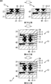
- the bonding process is performed by bonding the bonding pads 16 and bonding pads 17 to each other by metal bonding.
- the silicon substrate 21 of the upper substrate 12 is ground and polished from the upper side of FIG. 4, for example, the thickness of the upper substrate 12 becomes about 5 to 10 ⁇ m.
- the subsequent steps differ depending on the use of the multilayer device 11.
- the multilayer device 11 is created using the manufacturing method disclosed in Patent Document 3 described above.
- a process of connecting the bonding pad 17 to a circuit that electrically fixes the bonding pad 17 is performed.
- the multilayer device 11 having an electromagnetic wave shielding structure that blocks electromagnetic waves between the upper substrate 12 and the lower substrate 13 can be manufactured.
- the upper substrate 12 and the lower substrate 13 are bonded by metal bonding between the bonding pad 16 and the bonding pad 17, so that, for example, compared with a configuration in which a metal and an insulating film are bonded.
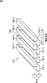
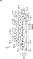
- FIG. 5 is a diagram illustrating a configuration example of the second embodiment of the multilayer device 11.
- FIG. 5 shows a bonding pad 16A and a bonding pad 17A formed on the bonding surface of the multilayer device 11A, and the other components are omitted because they are the same as the multilayer device 11.
- the manufacturing method of the multilayer device 11A is the same as that of the multilayer device 11 described with reference to FIGS.
- the bonding pad 16A and the bonding pad 17A are independently formed in a straight line, and the bonding pad 16A and the bonding pad 17A are metal-bonded to each other over the entire surface.
- the bonding pad 16A and the bonding pad 17A are formed in a pattern in which the length of the long side is 100 ⁇ m and the interval is 0.005 ⁇ m to 1000 ⁇ m.
- FIG. 5 also shows four bonding pads 16A-1 to 16A-4 and four bonding pads 17A-1 to 17A-4 among the bonding pads 16A and bonding pads 17A that are formed in plural. Yes. Adjacent ones of the bonding pads 16A-1 to 16A-4 are connected by a connecting wiring 18A formed in the same layer, and adjacent ones of the bonding pads 17A-1 to 17A-4 are connected. Are connected by a connecting wire 19A formed in the same layer. Furthermore, at least one of the bonding pads 16A-1 to 16A-4 and the bonding pads 17A-1 to 17A-4 is connected to a circuit that is electrically fixed. For example, in the configuration example of FIG. 5, the potential of the bonding pad 17A-4 is fixed.
- an electromagnetic wave shielding configuration can be configured by fixing the potential by metal bonding of the bonding pad 16A and the bonding pad 17A formed in a straight line. Thereby, in the multilayer device 11A, it is possible to suppress the noise caused by electromagnetic waves generated during operation from having an adverse effect.
- the electromagnetic wave shielding configuration constituted by the bonding pad 16A and the bonding pad 17A can be provided on the entire surface of the multilayer device 11A, for example.
- an electromagnetic wave shield configuration constituted by the bonding pad 16A and the bonding pad 17A is arranged in a region in the vicinity of a specific circuit that generates an electromagnetic wave having an adverse effect or a region in the vicinity of a specific circuit that is easily affected by an adverse effect. Also good.
- FIG. 6 is a diagram illustrating a configuration example of the third embodiment of the stacked device 11.
- FIG. 6 illustrates a bonding pad 16B and a bonding pad 17B formed on the bonding surface of the multilayer device 11B, and the other components are omitted because they are the same as those of the multilayer device 11.
- the manufacturing method of the multilayer device 11B is the same as that of the multilayer device 11 described with reference to FIGS.
- the bonding pad 16B and the bonding pad 17B are each independently formed in a linear shape, similarly to the multilayer device 11A of FIG.
- the bonding pad 16B and the bonding pad 17B are arranged at positions shifted from each other, and an electromagnetic wave shielding configuration is configured by metal-bonding portions of each to fix the potential.
- the bonding pad 16B-1 is disposed between the bonding pad 17B-1 and the bonding pad 17B-2, and is partially metal bonded at a portion overlapping the bonding pad 17B-1 and the bonding pad 17B-2.
- the bonding pad 17B-2 is disposed between the bonding pad 16B-2 and the bonding pad 16B-3, and is partially metal bonded at a portion overlapping the bonding pad 16B-2 and the bonding pad 16B-3.
- the bonding pads 16B and the bonding pads 17B are arranged at positions shifted from each other, that is, the bonding pads 17B are arranged at positions that close the intervals between the bonding pads 16B.
- the overlapping parts are partially metal bonded.
- the bonding surface is entirely covered with the bonding pad 16B and the bonding pad 17B, and when viewed from above or below, it looks as if the metal is disposed on the entire bonding surface. Configured as follows.
- noise due to electromagnetic waves generated during operation has an adverse effect due to the electromagnetic shield configuration configured to appear as if metal is disposed on the entire bonding surface. This can be more reliably suppressed.
- the electromagnetic wave shielding configuration constituted by the bonding pad 16B and the bonding pad 17B can be provided on the entire surface of the multilayer device 11B, for example.
- an electromagnetic wave shielding configuration constituted by the bonding pad 16B and the bonding pad 17B is disposed in a region in the vicinity of a specific circuit that generates an electromagnetic wave having an adverse effect or a region in the vicinity of a specific circuit that is easily affected by an adverse effect. Also good.
- FIG. 7 is a diagram illustrating a configuration example of the fourth embodiment of the multilayer device 11.
- FIG. 7 shows a bonding pad 16C and a bonding pad 17C formed on the bonding surface of the multilayer device 11C, and the other components are omitted because they are the same as those of the multilayer device 11.
- the manufacturing method of the multilayer device 11C is the same as that of the multilayer device 11 described with reference to FIGS.
- the bonding pad 16 ⁇ / b> C is linearly formed like the bonding pad 16 ⁇ / b> A of FIG. 5, and the bonding pad 17 ⁇ / b> C is rectangular like the bonding pad 17 of FIG. 1. It is formed.
- an electromagnetic wave shielding configuration can be configured by metal-bonding the bonding pad 16C formed in a straight line and the bonding pad 17C formed in a rectangular shape to fix the potential. . Thereby, in the multilayer device 11C, it can suppress more reliably that the noise by the electromagnetic waves generate
- the electromagnetic wave shielding configuration constituted by the bonding pad 16C and the bonding pad 17C can be provided on the entire surface of the multilayer device 11C, for example.
- an electromagnetic wave shield configuration constituted by the bonding pad 16C and the bonding pad 17C is arranged in a region in the vicinity of a specific circuit that generates an electromagnetic wave having an adverse effect or a region in the vicinity of a specific circuit that is easily affected by an adverse effect. Also good.
- the bonding pad 16C is formed in a rectangular shape like the bonding pad 17 in FIG. 1, and the bonding pad 17C is formed in a straight line like the bonding pad 16A in FIG. It is good also as a structure to be.
- FIG. 8 is a diagram illustrating a configuration example of the fifth embodiment of the multilayer device 11.
- FIGS. 8 shows a bonding pad 16D and a bonding pad 17D formed on the bonding surface of the multilayer device 11D, and the other components are omitted because they are the same as those of the multilayer device 11.
- the manufacturing method of the multilayer device 11D is the same as that of the multilayer device 11 described with reference to FIGS.
- the bonding pad 16D is formed in a straight line like the bonding pad 16A in FIG. 5, and the bonding pad 17D is formed in a rectangular shape like the bonding pad 17 in FIG. It is formed. Further, in the multilayer device 11D, as in the multilayer device 11B of FIG. 6, the bonding pad 16D and the bonding pad 17D are arranged at positions shifted from each other, and the respective portions are metal-bonded to fix the potential.
- An electromagnetic shielding configuration is configured.
- the bonding pad 16D and the bonding pad 17D are arranged at positions shifted from each other. For example, compared to the configuration of FIG. Can be arranged. Therefore, in the multilayer device 11D configured as described above, it is possible to more reliably suppress the adverse effect of noise caused by electromagnetic waves generated during operation.
- the electromagnetic wave shielding configuration constituted by the bonding pad 16D and the bonding pad 17D can be provided on the entire surface of the multilayer device 11D, for example.
- an electromagnetic wave shielding configuration constituted by the bonding pad 16D and the bonding pad 17D is disposed in a region near a specific circuit that generates an electromagnetic wave having an adverse effect or a region in the vicinity of a specific circuit that is easily affected by an adverse effect. Also good.
- the bonding pad 16D is formed in a rectangular shape like the bonding pad 17 in FIG. 1, and the bonding pad 17D is formed in a straight line like the bonding pad 16A in FIG. It is good also as a structure to be.
- FIG. 9 is a diagram illustrating a configuration example of the sixth embodiment of the multilayer device 11.
- connection wiring 19E is formed in a layer different from the bonding pad 16E and the bonding pad 17E, and the bonding pad 16E and the bonding pad 17E are electrically connected by the connection wiring 19E. It has become.
- the row in which the bonding pad 16E-1 and the bonding pad 17E-1 are arranged is connected by the connecting wiring 19E-1 and the potential is fixed. Further, the row where the bonding pad 16E-2 and the bonding pad 17E-2 are arranged is connected by the connection wiring 19E-2 and the potential is fixed, and the row where the bonding pad 16E-3 and the bonding pad 17E-3 are arranged is The potential is fixed by being connected by the connecting wiring 19E-3.
- connection wiring 19E that connects the bonding pad 16E and the bonding pad 17E is provided in a layer different from the bonding pad 16E and the bonding pad 17E, and an electromagnetic wave shielding configuration can be configured.
- the electromagnetic wave shielding configuration constituted by the bonding pad 16E and the bonding pad 17E can be provided on the entire surface of the multilayer device 11E, for example.
- an electromagnetic wave shield configuration constituted by the bonding pad 16E and the bonding pad 17E is arranged in a region in the vicinity of a specific circuit that generates an electromagnetic wave having an adverse effect or a region in the vicinity of a specific circuit that is easily affected by an adverse effect. Also good.
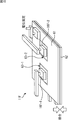
- FIG. 10 is a diagram illustrating a configuration example of the seventh embodiment of the multilayer device 11.
- the metal layer 61 is formed on the entire surface of the bonding surface 14 (see FIG. 1) of the upper substrate 12F, and the bonding surface 15 (see FIG. 1) of the lower substrate 13F.
- a metal layer 62 is formed on the entire surface.
- the connecting portion that electrically connects the upper substrate 12F and the lower substrate 13F is electrically independent from the metal layer 61 by, for example, a slit formed with a width of 0.01 to 100 ⁇ n. ing.
- a slit formed with a width of 0.01 to 100 ⁇ n.
- the slit 63-1 is formed so as to surround the bonding pad 16F-1 that is the connection portion
- the slit 63-2 is formed so as to surround the bonding pad 16F-2 that is the connection portion. Is done.
- the metal layer 61 and a part of the metal layer 62 are connected to a circuit in which the metal layer 61 is electrically fixed in the configuration example of FIG.
- the multilayer device 11F configured as described above has an electromagnetic wave shielding configuration configured by bonding and fixing the potential of the metal layer 61 and the metal layer 62, so that an electromagnetic wave is transmitted between the upper substrate 12F and the lower substrate 13F. , It can be cut off more reliably. Therefore, in the multilayer device 11F, it is possible to more reliably suppress the adverse effect of noise caused by electromagnetic waves generated during operation.
- the electromagnetic wave shielding configuration constituted by the metal layer 61 and the metal layer 62 can be provided on the entire surface of the multilayer device 11F, for example.
- an electromagnetic wave shielding configuration constituted by the metal layer 61 and the metal layer 62 is arranged in a region in the vicinity of a specific circuit that generates an electromagnetic wave having an adverse effect or a region in the vicinity of a specific circuit that is likely to be adversely affected. Also good.
- the RF sputtering process or the vapor deposition process is performed on the wiring layer 22 on which the bonding pad 16F is formed in the seventh process shown in FIG.
- the metal layer 61 is formed using Similarly, on the lower substrate 13F, a metal layer 62 is formed on the wiring layer 42 on which the bonding pads 17F are formed.
- the metal layer 61 and the metal layer 62 are made to have a thickness of 0.1 to 1000 nm using a conductive metal material such as Cu, CuO, Ta, TaN, Ti, TiN, W, WN, Ru, RuN, and Co. A film is formed.
- the resist 71 is applied to the metal layer 61
- the resist is surrounded by the general lithography technique so as to surround the bonding pad 16F.
- An opening 72 is opened at 71.
- an opening 82 is opened in the resist 81 so as to surround the bonding pad 17F.
- the metal layer 61 and the metal layer 62 are metal-bonded to each other so as to bond the upper substrate 12F and the lower substrate 13F.
- the bonding pad 16F and the bonding pad 17F are bonded by the slit 63 and the slit 64 independently of the metal layer 61 and the metal layer 62.
- the silicon substrate 21 of the upper substrate 12F is ground and polished from the upper side of FIG. 12, for example, the thickness of the upper substrate 12F is about 5 to 10 ⁇ m.
- the subsequent steps differ depending on the use of the multilayer device 11F.
- the multilayer device 11F is created using the manufacturing method disclosed in Patent Document 3 described above.
- the multilayer device 11F having an electromagnetic wave shielding structure that blocks electromagnetic waves between the upper substrate 12F and the lower substrate 13F can be manufactured. Further, in the multilayer device 11F, the upper substrate 12F and the lower substrate 13F are bonded by metal bonding with the metal layer 61 and the metal layer 62, so that, for example, compared with a configuration in which a metal and an insulating film are bonded. As a result, it is possible to avoid the occurrence of wafer cracking during production, for example, by increasing the bonding force.
- the multilayer device 11 having a two-layer structure has been described.
- the present technology can be applied to the multilayer device 11 in which three or more substrates are stacked.
- the method of arranging the electromagnetic wave shielding structure and the arrangement position of the electromagnetic wave shield structure the above-described configuration examples can be appropriately selected and combined.
- the stacked device 11 of each embodiment as described above can be applied to, for example, a solid-state imaging device that captures an image.
- the solid-state imaging device configured as the stacked device 11 includes various imaging devices such as an imaging system such as a digital still camera and a digital video camera, a mobile phone having an imaging function, or other devices having an imaging function. It can be applied to electronic equipment.
- FIG. 13 is a block diagram illustrating a configuration example of an imaging device mounted on an electronic device.
- the imaging apparatus 101 includes an optical system 102, an imaging element 103, a signal processing circuit 104, a monitor 105, and a memory 106, and can capture still images and moving images.
- the optical system 102 includes one or more lenses, guides image light (incident light) from a subject to the image sensor 103, and forms an image on a light receiving surface (sensor unit) of the image sensor 103.
- the image sensor 103 is configured as the stacked device 11 of each embodiment described above.
- electrons are accumulated for a certain period according to an image formed on the light receiving surface via the optical system 102. Then, a signal corresponding to the electrons accumulated in the image sensor 103 is supplied to the signal processing circuit 104.
- the signal processing circuit 104 performs various signal processing on the pixel signal output from the image sensor 103.
- An image (image data) obtained by performing signal processing by the signal processing circuit 104 is supplied to the monitor 105 and displayed, or supplied to the memory 106 and stored (recorded).
- a high-quality image with less noise can be captured by applying the stacked device 11 of each of the above-described embodiments.
- this technique can also take the following structures.
- the first metal layer is formed so as to be exposed at a joint surface that joins the one substrate to the other substrate;
- each of the first metal layer and the second metal layer includes a plurality of pads that are independently arranged at a predetermined interval.
- At least a part of the plurality of pads constituting each of the first metal layer and the second metal layer is formed in the same layer as each of the first metal layer and the second metal layer.
- the stacked device according to (3), wherein the stacked device is electrically connected to the stacked device.
- the plurality of pads constituting the first metal layer and the plurality of pads constituting the second metal layer are bonded to each other in whole or in part.
- At least a part of the plurality of pads constituting each of the first metal layer and the second metal layer is via a wiring in a different layer different from the first metal layer and the second metal layer.
- the stacked device according to (3) which is electrically connected.
- the first metal layer and the second metal layer are formed on the entire surface other than a joint portion that performs electrical connection between the one substrate and the other substrate,
- the electromagnetic wave shielding structure is generated in a region where electromagnetic waves that adversely affect the operation of the other substrate from the one substrate or in the other substrate on the bonding surface of the one substrate and the other substrate.
- the multilayer device according to any one of (1) to (7), wherein the multilayer device is disposed in at least one of the regions adversely affected by the electromagnetic wave on the one substrate.
- (10) Forming a first metal layer on one of a plurality of substrates stacked in at least two layers; Forming a second metal layer on the other substrate laminated to the one substrate; Forming an electromagnetic wave shielding structure for blocking electromagnetic waves between the one substrate and the other substrate by bonding and fixing the potential of the first metal layer and the second metal layer.
- a manufacturing method of a stacked device A manufacturing method of a stacked device.
- Electronic equipment comprising.
Landscapes
- Engineering & Computer Science (AREA)
- Multimedia (AREA)
- Signal Processing (AREA)
- Shielding Devices Or Components To Electric Or Magnetic Fields (AREA)
- Solid State Image Pick-Up Elements (AREA)
- Internal Circuitry In Semiconductor Integrated Circuit Devices (AREA)
- Semiconductor Integrated Circuits (AREA)
Abstract
Description
(1)
少なくとも2層以上で積層される複数の基板のうちの一方の基板に形成される第1の金属層と、
前記一方の基板に対して積層される他方の基板に形成される第2の金属層と
を備え、
前記第1の金属層と前記第2の金属層とを接合して電位固定することによって、前記一方の基板と前記他方の基板との間で電磁波を遮断する電磁波シールド構造を構成する
積層型デバイス。
(2)
前記第1の金属層は、前記一方の基板を前記他方の基板に接合する接合面に露出するように形成され、
前記第2の金属層は、前記他方の基板を前記一方の基板に接合する接合面に露出するように形成される
上記(1)に記載の積層型デバイス。
(3)
前記第1の金属層および前記第2の金属層は、所定間隔で独立して配置された複数のパッドにより、それぞれ構成される
上記(1)または(2)に記載の積層型デバイス。
(4)
前記第1の金属層および前記第2の金属層それぞれを構成する複数の前記パッドの少なくとも一部は、前記第1の金属層および前記第2の金属層それぞれと同一層に形成される連結配線によって電気的に接続される
上記(3)に記載の積層型デバイス。
(5)
前記第1の金属層を構成する複数の前記パッドと、前記第2の金属層を構成する複数の前記パッドとは、互いに全面または一部で接合される
上記(3)または(4)のいずれかに記載の積層型デバイス。
(6)
前記第1の金属層および前記第2の金属層それぞれを構成する複数の前記パッドの少なくとも一部は、前記第1の金属層および前記第2の金属層とは異なる別層の配線を介して電気的に接続される
上記(3)に記載の積層型デバイス。
(7)
前記第1の金属層および前記第2の金属層は、前記一方の基板と前記他方の基板との間で電気的な接続を行う接合部以外の全面に形成され、
前記第1の金属層と前記接合部との間、および、前記第2の金属層と前記接合部との間にスリットが形成される
上記(1)または(2)に記載の積層型デバイス。
(8)
前記電磁波シールド構造は、前記一方の基板および前記他方の基板の接合面の全面に配置される
上記(1)から(7)までのいずれかに記載の積層型デバイス。
(9)
前記電磁波シールド構造は、前記一方の基板および前記他方の基板の接合面における、前記一方の基板から前記他方の基板の動作に悪影響を与える電磁波を発生する領域、または、前記他方の基板において発生する電磁波により前記一方の基板において悪影響を受ける領域のうち、少なくともいずれか一方の領域に配置される
上記(1)から(7)までのいずれかに記載の積層型デバイス。
(10)
少なくとも2層以上で積層される複数の基板のうちの一方の基板に第1の金属層を形成し、
前記一方の基板に対して積層される他方の基板に第2の金属層を形成し、
前記第1の金属層と前記第2の金属層とを接合して電位固定することによって、前記一方の基板と前記他方の基板との間で電磁波を遮断する電磁波シールド構造を構成する
ステップを含む積層型デバイスの製造方法。
(11)
少なくとも2層以上で積層される複数の基板のうちの一方の基板に形成される第1の金属層と、
前記一方の基板に対して積層される他方の基板に形成される第2の金属層と
を有し、
前記第1の金属層と前記第2の金属層とを接合して電位固定することによって、前記一方の基板と前記他方の基板との間で電磁波を遮断する電磁波シールド構造を構成する
積層型デバイスを備える電子機器。
Claims (11)
- 少なくとも2層以上で積層される複数の基板のうちの一方の基板に形成される第1の金属層と、
前記一方の基板に対して積層される他方の基板に形成される第2の金属層と
を備え、
前記第1の金属層と前記第2の金属層とを接合して電位固定することによって、前記一方の基板と前記他方の基板との間で電磁波を遮断する電磁波シールド構造を構成する
積層型デバイス。 - 前記第1の金属層は、前記一方の基板を前記他方の基板に接合する接合面に露出するように形成され、
前記第2の金属層は、前記他方の基板を前記一方の基板に接合する接合面に露出するように形成される
請求項1に記載の積層型デバイス。 - 前記第1の金属層および前記第2の金属層は、所定間隔で独立して配置された複数のパッドにより、それぞれ構成される
請求項2に記載の積層型デバイス。 - 前記第1の金属層および前記第2の金属層それぞれを構成する複数の前記パッドの少なくとも一部は、前記第1の金属層および前記第2の金属層それぞれと同一層に形成される連結配線によって電気的に接続される
請求項3に記載の積層型デバイス。 - 前記第1の金属層を構成する複数の前記パッドと、前記第2の金属層を構成する複数の前記パッドとは、互いに全面または一部で接合される
請求項3に記載の積層型デバイス。 - 前記第1の金属層および前記第2の金属層それぞれを構成する複数の前記パッドの少なくとも一部は、前記第1の金属層および前記第2の金属層とは異なる別層の配線を介して電気的に接続される
請求項3に記載の積層型デバイス。 - 前記第1の金属層および前記第2の金属層は、前記一方の基板と前記他方の基板との間で電気的な接続を行う接合部以外の全面に形成され、
前記第1の金属層と前記接合部との間、および、前記第2の金属層と前記接合部との間にスリットが形成される
請求項2に記載の積層型デバイス。 - 前記電磁波シールド構造は、前記一方の基板および前記他方の基板の接合面の全面に配置される
請求項1に記載の積層型デバイス。 - 前記電磁波シールド構造は、前記一方の基板および前記他方の基板の接合面における、前記一方の基板から前記他方の基板の動作に悪影響を与える電磁波を発生する領域、または、前記他方の基板において発生する電磁波により前記一方の基板において悪影響を受ける領域のうち、少なくともいずれか一方の領域に配置される
請求項1に記載の積層型デバイス。 - 少なくとも2層以上で積層される複数の基板のうちの一方の基板に第1の金属層を形成し、
前記一方の基板に対して積層される他方の基板に第2の金属層を形成し、
前記第1の金属層と前記第2の金属層とを接合して電位固定することによって、前記一方の基板と前記他方の基板との間で電磁波を遮断する電磁波シールド構造を構成する
ステップを含む積層型デバイスの製造方法。 - 少なくとも2層以上で積層される複数の基板のうちの一方の基板に形成される第1の金属層と、
前記一方の基板に対して積層される他方の基板に形成される第2の金属層と
を有し、
前記第1の金属層と前記第2の金属層とを接合して電位固定することによって、前記一方の基板と前記他方の基板との間で電磁波を遮断する電磁波シールド構造を構成する
積層型デバイスを備える電子機器。
Priority Applications (4)
| Application Number | Priority Date | Filing Date | Title |
|---|---|---|---|
| US15/514,870 US20170243819A1 (en) | 2014-10-08 | 2015-09-28 | Stacked device, manufacturing method, and electronic instrument |
| KR1020177008139A KR102426811B1 (ko) | 2014-10-08 | 2015-09-28 | 적층형 디바이스 및 제조 방법, 및, 전자 기기 |
| JP2016553045A JP6683619B2 (ja) | 2014-10-08 | 2015-09-28 | 半導体装置および製造方法、並びに、電子機器 |
| CN201580052391.4A CN107078056A (zh) | 2014-10-08 | 2015-09-28 | 层叠型装置、制造方法及电子设备 |
Applications Claiming Priority (2)
| Application Number | Priority Date | Filing Date | Title |
|---|---|---|---|
| JP2014-207129 | 2014-10-08 | ||
| JP2014207129 | 2014-10-08 |
Publications (1)
| Publication Number | Publication Date |
|---|---|
| WO2016056409A1 true WO2016056409A1 (ja) | 2016-04-14 |
Family
ID=55653026
Family Applications (1)
| Application Number | Title | Priority Date | Filing Date |
|---|---|---|---|
| PCT/JP2015/077241 Ceased WO2016056409A1 (ja) | 2014-10-08 | 2015-09-28 | 積層型デバイスおよび製造方法、並びに、電子機器 |
Country Status (6)
| Country | Link |
|---|---|
| US (1) | US20170243819A1 (ja) |
| JP (2) | JP6683619B2 (ja) |
| KR (1) | KR102426811B1 (ja) |
| CN (1) | CN107078056A (ja) |
| TW (1) | TWI747805B (ja) |
| WO (1) | WO2016056409A1 (ja) |
Cited By (8)
| Publication number | Priority date | Publication date | Assignee | Title |
|---|---|---|---|---|
| CN107546174A (zh) * | 2017-07-28 | 2018-01-05 | 中国科学院微电子研究所 | 一种集成电路元器件的工艺方法 |
| CN109923671A (zh) * | 2016-11-14 | 2019-06-21 | 索尼半导体解决方案公司 | 固态图像传感器、其制造方法和电子设备 |
| WO2019235400A1 (ja) * | 2018-06-05 | 2019-12-12 | ソニーセミコンダクタソリューションズ株式会社 | 固体撮像装置、固体撮像装置の製造方法及び電子機器 |
| JP2020072410A (ja) * | 2018-10-31 | 2020-05-07 | ソニーセミコンダクタソリューションズ株式会社 | 固体撮像装置及び電子機器 |
| WO2020137606A1 (ja) * | 2018-12-26 | 2020-07-02 | ソニーセミコンダクタソリューションズ株式会社 | 半導体装置および電子機器 |
| JP2020123731A (ja) * | 2014-10-08 | 2020-08-13 | ソニーセミコンダクタソリューションズ株式会社 | 半導体装置および製造方法、並びに、電子機器 |
| WO2021095420A1 (ja) * | 2019-11-11 | 2021-05-20 | ソニーセミコンダクタソリューションズ株式会社 | 半導体装置及び電子機器 |
| WO2021256114A1 (ja) * | 2020-06-17 | 2021-12-23 | ソニーセミコンダクタソリューションズ株式会社 | 固体撮像装置 |
Families Citing this family (5)
| Publication number | Priority date | Publication date | Assignee | Title |
|---|---|---|---|---|
| US11508665B2 (en) * | 2020-06-23 | 2022-11-22 | Taiwan Semiconductor Manufacturing Co., Ltd. | Packages with thick RDLs and thin RDLs stacked alternatingly |
| JPWO2022097427A1 (ja) * | 2020-11-09 | 2022-05-12 | ||
| KR102887278B1 (ko) | 2020-12-17 | 2025-11-17 | 삼성전자주식회사 | 이미지 센서 |
| CN118160095A (zh) * | 2021-12-10 | 2024-06-07 | 索尼半导体解决方案公司 | 成像装置 |
| JP2023142256A (ja) * | 2022-03-24 | 2023-10-05 | ソニーセミコンダクタソリューションズ株式会社 | 固体撮像装置及び半導体装置の製造方法 |
Citations (4)
| Publication number | Priority date | Publication date | Assignee | Title |
|---|---|---|---|---|
| JPH1168029A (ja) * | 1997-08-14 | 1999-03-09 | Sumitomo Electric Ind Ltd | 半導体装置 |
| JP2006303220A (ja) * | 2005-04-21 | 2006-11-02 | Nec Electronics Corp | 半導体装置 |
| JP2008205975A (ja) * | 2007-02-21 | 2008-09-04 | Fujitsu Ltd | 半導体集積回路 |
| JP2012256736A (ja) * | 2011-06-09 | 2012-12-27 | Sony Corp | 半導体装置 |
Family Cites Families (21)
| Publication number | Priority date | Publication date | Assignee | Title |
|---|---|---|---|---|
| JP3532788B2 (ja) | 1999-04-13 | 2004-05-31 | 唯知 須賀 | 半導体装置及びその製造方法 |
| JP2002198686A (ja) * | 2000-12-27 | 2002-07-12 | Sony Corp | 電子部品用シートおよびその製造方法 |
| US6737750B1 (en) * | 2001-12-07 | 2004-05-18 | Amkor Technology, Inc. | Structures for improving heat dissipation in stacked semiconductor packages |
| JP3864927B2 (ja) * | 2003-04-14 | 2007-01-10 | ソニー株式会社 | 配線基板と回路モジュール |
| JP4250038B2 (ja) * | 2003-08-20 | 2009-04-08 | シャープ株式会社 | 半導体集積回路 |
| JP4577228B2 (ja) * | 2006-02-09 | 2010-11-10 | セイコーエプソン株式会社 | 半導体装置および半導体装置の製造方法 |
| JP4835710B2 (ja) * | 2009-03-17 | 2011-12-14 | ソニー株式会社 | 固体撮像装置、固体撮像装置の製造方法、固体撮像装置の駆動方法、及び電子機器 |
| JP5985136B2 (ja) * | 2009-03-19 | 2016-09-06 | ソニー株式会社 | 半導体装置とその製造方法、及び電子機器 |
| JP5458690B2 (ja) * | 2009-06-22 | 2014-04-02 | ソニー株式会社 | 固体撮像装置およびカメラ |
| JP5442394B2 (ja) | 2009-10-29 | 2014-03-12 | ソニー株式会社 | 固体撮像装置とその製造方法、及び電子機器 |
| JP5693060B2 (ja) * | 2010-06-30 | 2015-04-01 | キヤノン株式会社 | 固体撮像装置、及び撮像システム |
| JP2012064709A (ja) * | 2010-09-15 | 2012-03-29 | Sony Corp | 固体撮像装置及び電子機器 |
| JP5696513B2 (ja) | 2011-02-08 | 2015-04-08 | ソニー株式会社 | 固体撮像装置とその製造方法、及び電子機器 |
| KR101952976B1 (ko) * | 2011-05-24 | 2019-02-27 | 소니 주식회사 | 반도체 장치 |
| JP5970747B2 (ja) | 2011-05-24 | 2016-08-17 | ソニー株式会社 | 半導体装置 |
| JPWO2013080769A1 (ja) * | 2011-12-01 | 2015-04-27 | シャープ株式会社 | 固体撮像素子 |
| US8933544B2 (en) * | 2012-07-12 | 2015-01-13 | Omnivision Technologies, Inc. | Integrated circuit stack with integrated electromagnetic interference shielding |
| JP2014022561A (ja) | 2012-07-18 | 2014-02-03 | Sony Corp | 固体撮像装置、及び、電子機器 |
| JPWO2014080625A1 (ja) * | 2012-11-22 | 2017-01-05 | 株式会社ニコン | 撮像素子および撮像ユニット |
| JP2014165396A (ja) | 2013-02-26 | 2014-09-08 | Sony Corp | 固体撮像装置および電子機器 |
| TWI747805B (zh) * | 2014-10-08 | 2021-12-01 | 日商索尼半導體解決方案公司 | 攝像裝置及製造方法、以及電子機器 |
-
2015
- 2015-08-18 TW TW104126864A patent/TWI747805B/zh active
- 2015-09-28 US US15/514,870 patent/US20170243819A1/en not_active Abandoned
- 2015-09-28 WO PCT/JP2015/077241 patent/WO2016056409A1/ja not_active Ceased
- 2015-09-28 KR KR1020177008139A patent/KR102426811B1/ko active Active
- 2015-09-28 CN CN201580052391.4A patent/CN107078056A/zh active Pending
- 2015-09-28 JP JP2016553045A patent/JP6683619B2/ja active Active
-
2020
- 2020-03-30 JP JP2020059327A patent/JP7095013B2/ja not_active Expired - Fee Related
Patent Citations (4)
| Publication number | Priority date | Publication date | Assignee | Title |
|---|---|---|---|---|
| JPH1168029A (ja) * | 1997-08-14 | 1999-03-09 | Sumitomo Electric Ind Ltd | 半導体装置 |
| JP2006303220A (ja) * | 2005-04-21 | 2006-11-02 | Nec Electronics Corp | 半導体装置 |
| JP2008205975A (ja) * | 2007-02-21 | 2008-09-04 | Fujitsu Ltd | 半導体集積回路 |
| JP2012256736A (ja) * | 2011-06-09 | 2012-12-27 | Sony Corp | 半導体装置 |
Cited By (13)
| Publication number | Priority date | Publication date | Assignee | Title |
|---|---|---|---|---|
| JP2020123731A (ja) * | 2014-10-08 | 2020-08-13 | ソニーセミコンダクタソリューションズ株式会社 | 半導体装置および製造方法、並びに、電子機器 |
| CN109923671A (zh) * | 2016-11-14 | 2019-06-21 | 索尼半导体解决方案公司 | 固态图像传感器、其制造方法和电子设备 |
| US12446348B2 (en) | 2016-11-14 | 2025-10-14 | Sony Semiconductor Solutions Corporation | Solid-state imaging element, manufacturing method, and electronic device |
| CN107546174A (zh) * | 2017-07-28 | 2018-01-05 | 中国科学院微电子研究所 | 一种集成电路元器件的工艺方法 |
| WO2019235400A1 (ja) * | 2018-06-05 | 2019-12-12 | ソニーセミコンダクタソリューションズ株式会社 | 固体撮像装置、固体撮像装置の製造方法及び電子機器 |
| US12199121B2 (en) | 2018-06-05 | 2025-01-14 | Sony Semiconductor Solutions Corporation | Solid-state imaging device with increased bonding strength, and method of manufacturing the solid-state imaging device |
| JP2020072410A (ja) * | 2018-10-31 | 2020-05-07 | ソニーセミコンダクタソリューションズ株式会社 | 固体撮像装置及び電子機器 |
| US11792551B2 (en) | 2018-10-31 | 2023-10-17 | Sony Semiconductor Solutions Corporation | Stacked light receiving sensor and electronic apparatus |
| JP7402606B2 (ja) | 2018-10-31 | 2023-12-21 | ソニーセミコンダクタソリューションズ株式会社 | 固体撮像装置及び電子機器 |
| WO2020090509A1 (ja) * | 2018-10-31 | 2020-05-07 | ソニーセミコンダクタソリューションズ株式会社 | 積層型受光センサ及び電子機器 |
| WO2020137606A1 (ja) * | 2018-12-26 | 2020-07-02 | ソニーセミコンダクタソリューションズ株式会社 | 半導体装置および電子機器 |
| WO2021095420A1 (ja) * | 2019-11-11 | 2021-05-20 | ソニーセミコンダクタソリューションズ株式会社 | 半導体装置及び電子機器 |
| WO2021256114A1 (ja) * | 2020-06-17 | 2021-12-23 | ソニーセミコンダクタソリューションズ株式会社 | 固体撮像装置 |
Also Published As
| Publication number | Publication date |
|---|---|
| CN107078056A (zh) | 2017-08-18 |
| KR20170070018A (ko) | 2017-06-21 |
| KR102426811B1 (ko) | 2022-07-29 |
| TWI747805B (zh) | 2021-12-01 |
| JP7095013B2 (ja) | 2022-07-04 |
| JP6683619B2 (ja) | 2020-04-22 |
| US20170243819A1 (en) | 2017-08-24 |
| TW201626460A (zh) | 2016-07-16 |
| JP2020123731A (ja) | 2020-08-13 |
| JPWO2016056409A1 (ja) | 2017-07-20 |
Similar Documents
| Publication | Publication Date | Title |
|---|---|---|
| JP7095013B2 (ja) | 半導体装置および製造方法、並びに、電子機器 | |
| US12125867B2 (en) | Imaging device and electronic device | |
| JP5994274B2 (ja) | 半導体装置、半導体装置の製造方法、及び、電子機器 | |
| JP5682327B2 (ja) | 固体撮像素子、固体撮像素子の製造方法、及び電子機器 | |
| US9024405B2 (en) | Solid-state image sensor | |
| JP5696513B2 (ja) | 固体撮像装置とその製造方法、及び電子機器 | |
| JP5513872B2 (ja) | 固体撮像装置 | |
| KR101411800B1 (ko) | 고체 촬상 장치 및 촬상 시스템 | |
| KR102079407B1 (ko) | 반도체 장치의 제조 방법 | |
| JP5187284B2 (ja) | 半導体装置の製造方法 | |
| JP5296406B2 (ja) | 固体撮像装置及びその製造方法 | |
| WO2021090545A1 (ja) | 撮像素子および撮像装置 | |
| JP7535707B2 (ja) | 撮像装置 | |
| JP5950531B2 (ja) | 半導体装置の製造方法及び半導体ウエハ | |
| WO2021199665A1 (ja) | 固体撮像装置及び固体撮像装置の製造方法、並びに電子機器 |
Legal Events
| Date | Code | Title | Description |
|---|---|---|---|
| 121 | Ep: the epo has been informed by wipo that ep was designated in this application |
Ref document number: 15849081 Country of ref document: EP Kind code of ref document: A1 |
|
| ENP | Entry into the national phase |
Ref document number: 2016553045 Country of ref document: JP Kind code of ref document: A |
|
| ENP | Entry into the national phase |
Ref document number: 20177008139 Country of ref document: KR Kind code of ref document: A |
|
| WWE | Wipo information: entry into national phase |
Ref document number: 15514870 Country of ref document: US |
|
| NENP | Non-entry into the national phase |
Ref country code: DE |
|
| 122 | Ep: pct application non-entry in european phase |
Ref document number: 15849081 Country of ref document: EP Kind code of ref document: A1 |