WO2016027564A1 - 半導体装置及び半導体装置の製造方法 - Google Patents
半導体装置及び半導体装置の製造方法 Download PDFInfo
- Publication number
- WO2016027564A1 WO2016027564A1 PCT/JP2015/068095 JP2015068095W WO2016027564A1 WO 2016027564 A1 WO2016027564 A1 WO 2016027564A1 JP 2015068095 W JP2015068095 W JP 2015068095W WO 2016027564 A1 WO2016027564 A1 WO 2016027564A1
- Authority
- WO
- WIPO (PCT)
- Prior art keywords
- electrode
- insulating film
- semiconductor substrate
- interlayer insulating
- schottky
- Prior art date
Links
- 239000004065 semiconductor Substances 0.000 title claims abstract description 136
- 238000004519 manufacturing process Methods 0.000 title claims description 24
- 239000011229 interlayer Substances 0.000 claims abstract description 78
- 239000000758 substrate Substances 0.000 claims abstract description 71
- 229910052751 metal Inorganic materials 0.000 claims abstract description 33
- 239000002184 metal Substances 0.000 claims abstract description 33
- 238000005530 etching Methods 0.000 claims description 33
- 239000010410 layer Substances 0.000 claims description 28
- 230000004888 barrier function Effects 0.000 claims description 26
- 238000000034 method Methods 0.000 claims description 14
- 210000000746 body region Anatomy 0.000 description 27
- 238000010586 diagram Methods 0.000 description 10
- 239000012535 impurity Substances 0.000 description 6
- 239000000463 material Substances 0.000 description 6
- 229910018503 SF6 Inorganic materials 0.000 description 5
- SFZCNBIFKDRMGX-UHFFFAOYSA-N sulfur hexafluoride Chemical compound FS(F)(F)(F)(F)F SFZCNBIFKDRMGX-UHFFFAOYSA-N 0.000 description 5
- NRTOMJZYCJJWKI-UHFFFAOYSA-N Titanium nitride Chemical compound [Ti]#N NRTOMJZYCJJWKI-UHFFFAOYSA-N 0.000 description 3
- 238000005516 engineering process Methods 0.000 description 3
- KDLHZDBZIXYQEI-UHFFFAOYSA-N palladium Substances [Pd] KDLHZDBZIXYQEI-UHFFFAOYSA-N 0.000 description 3
- 238000011084 recovery Methods 0.000 description 2
- 229960000909 sulfur hexafluoride Drugs 0.000 description 2
- 229910052782 aluminium Inorganic materials 0.000 description 1
- XAGFODPZIPBFFR-UHFFFAOYSA-N aluminium Chemical compound [Al] XAGFODPZIPBFFR-UHFFFAOYSA-N 0.000 description 1
- 230000015572 biosynthetic process Effects 0.000 description 1
- 239000003795 chemical substances by application Substances 0.000 description 1
- 238000005468 ion implantation Methods 0.000 description 1
- 238000012986 modification Methods 0.000 description 1
- 230000004048 modification Effects 0.000 description 1
- 229910052763 palladium Inorganic materials 0.000 description 1
- 238000004544 sputter deposition Methods 0.000 description 1
- WFKWXMTUELFFGS-UHFFFAOYSA-N tungsten Chemical compound [W] WFKWXMTUELFFGS-UHFFFAOYSA-N 0.000 description 1
- 229910052721 tungsten Inorganic materials 0.000 description 1
- 239000010937 tungsten Substances 0.000 description 1
Images


Classifications
-
- H—ELECTRICITY
- H10—SEMICONDUCTOR DEVICES; ELECTRIC SOLID-STATE DEVICES NOT OTHERWISE PROVIDED FOR
- H10D—INORGANIC ELECTRIC SEMICONDUCTOR DEVICES
- H10D84/00—Integrated devices formed in or on semiconductor substrates that comprise only semiconducting layers, e.g. on Si wafers or on GaAs-on-Si wafers
- H10D84/40—Integrated devices formed in or on semiconductor substrates that comprise only semiconducting layers, e.g. on Si wafers or on GaAs-on-Si wafers characterised by the integration of at least one component covered by groups H10D12/00 or H10D30/00 with at least one component covered by groups H10D10/00 or H10D18/00, e.g. integration of IGFETs with BJTs
- H10D84/401—Combinations of FETs or IGBTs with BJTs
- H10D84/403—Combinations of FETs or IGBTs with BJTs and with one or more of diodes, resistors or capacitors
-
- H—ELECTRICITY
- H10—SEMICONDUCTOR DEVICES; ELECTRIC SOLID-STATE DEVICES NOT OTHERWISE PROVIDED FOR
- H10D—INORGANIC ELECTRIC SEMICONDUCTOR DEVICES
- H10D64/00—Electrodes of devices having potential barriers
- H10D64/20—Electrodes characterised by their shapes, relative sizes or dispositions
-
- H—ELECTRICITY
- H01—ELECTRIC ELEMENTS
- H01L—SEMICONDUCTOR DEVICES NOT COVERED BY CLASS H10
- H01L21/00—Processes or apparatus adapted for the manufacture or treatment of semiconductor or solid state devices or of parts thereof
- H01L21/02—Manufacture or treatment of semiconductor devices or of parts thereof
- H01L21/04—Manufacture or treatment of semiconductor devices or of parts thereof the devices having potential barriers, e.g. a PN junction, depletion layer or carrier concentration layer
- H01L21/18—Manufacture or treatment of semiconductor devices or of parts thereof the devices having potential barriers, e.g. a PN junction, depletion layer or carrier concentration layer the devices having semiconductor bodies comprising elements of Group IV of the Periodic Table or AIIIBV compounds with or without impurities, e.g. doping materials
- H01L21/28—Manufacture of electrodes on semiconductor bodies using processes or apparatus not provided for in groups H01L21/20 - H01L21/268
-
- H—ELECTRICITY
- H10—SEMICONDUCTOR DEVICES; ELECTRIC SOLID-STATE DEVICES NOT OTHERWISE PROVIDED FOR
- H10D—INORGANIC ELECTRIC SEMICONDUCTOR DEVICES
- H10D30/00—Field-effect transistors [FET]
- H10D30/01—Manufacture or treatment
- H10D30/021—Manufacture or treatment of FETs having insulated gates [IGFET]
- H10D30/028—Manufacture or treatment of FETs having insulated gates [IGFET] of double-diffused metal oxide semiconductor [DMOS] FETs
- H10D30/0291—Manufacture or treatment of FETs having insulated gates [IGFET] of double-diffused metal oxide semiconductor [DMOS] FETs of vertical DMOS [VDMOS] FETs
- H10D30/0297—Manufacture or treatment of FETs having insulated gates [IGFET] of double-diffused metal oxide semiconductor [DMOS] FETs of vertical DMOS [VDMOS] FETs using recessing of the gate electrodes, e.g. to form trench gate electrodes
-
- H—ELECTRICITY
- H10—SEMICONDUCTOR DEVICES; ELECTRIC SOLID-STATE DEVICES NOT OTHERWISE PROVIDED FOR
- H10D—INORGANIC ELECTRIC SEMICONDUCTOR DEVICES
- H10D30/00—Field-effect transistors [FET]
- H10D30/60—Insulated-gate field-effect transistors [IGFET]
-
- H—ELECTRICITY
- H10—SEMICONDUCTOR DEVICES; ELECTRIC SOLID-STATE DEVICES NOT OTHERWISE PROVIDED FOR
- H10D—INORGANIC ELECTRIC SEMICONDUCTOR DEVICES
- H10D30/00—Field-effect transistors [FET]
- H10D30/60—Insulated-gate field-effect transistors [IGFET]
- H10D30/64—Double-diffused metal-oxide semiconductor [DMOS] FETs
- H10D30/66—Vertical DMOS [VDMOS] FETs
- H10D30/668—Vertical DMOS [VDMOS] FETs having trench gate electrodes, e.g. UMOS transistors
-
- H—ELECTRICITY
- H10—SEMICONDUCTOR DEVICES; ELECTRIC SOLID-STATE DEVICES NOT OTHERWISE PROVIDED FOR
- H10D—INORGANIC ELECTRIC SEMICONDUCTOR DEVICES
- H10D62/00—Semiconductor bodies, or regions thereof, of devices having potential barriers
- H10D62/10—Shapes, relative sizes or dispositions of the regions of the semiconductor bodies; Shapes of the semiconductor bodies
- H10D62/17—Semiconductor regions connected to electrodes not carrying current to be rectified, amplified or switched, e.g. channel regions
- H10D62/393—Body regions of DMOS transistors or IGBTs
-
- H—ELECTRICITY
- H10—SEMICONDUCTOR DEVICES; ELECTRIC SOLID-STATE DEVICES NOT OTHERWISE PROVIDED FOR
- H10D—INORGANIC ELECTRIC SEMICONDUCTOR DEVICES
- H10D64/00—Electrodes of devices having potential barriers
- H10D64/20—Electrodes characterised by their shapes, relative sizes or dispositions
- H10D64/23—Electrodes carrying the current to be rectified, amplified, oscillated or switched, e.g. sources, drains, anodes or cathodes
- H10D64/251—Source or drain electrodes for field-effect devices
- H10D64/252—Source or drain electrodes for field-effect devices for vertical or pseudo-vertical devices
-
- H—ELECTRICITY
- H10—SEMICONDUCTOR DEVICES; ELECTRIC SOLID-STATE DEVICES NOT OTHERWISE PROVIDED FOR
- H10D—INORGANIC ELECTRIC SEMICONDUCTOR DEVICES
- H10D8/00—Diodes
-
- H—ELECTRICITY
- H10—SEMICONDUCTOR DEVICES; ELECTRIC SOLID-STATE DEVICES NOT OTHERWISE PROVIDED FOR
- H10D—INORGANIC ELECTRIC SEMICONDUCTOR DEVICES
- H10D8/00—Diodes
- H10D8/50—PIN diodes
-
- H—ELECTRICITY
- H10—SEMICONDUCTOR DEVICES; ELECTRIC SOLID-STATE DEVICES NOT OTHERWISE PROVIDED FOR
- H10D—INORGANIC ELECTRIC SEMICONDUCTOR DEVICES
- H10D8/00—Diodes
- H10D8/60—Schottky-barrier diodes
-
- H—ELECTRICITY
- H10—SEMICONDUCTOR DEVICES; ELECTRIC SOLID-STATE DEVICES NOT OTHERWISE PROVIDED FOR
- H10D—INORGANIC ELECTRIC SEMICONDUCTOR DEVICES
- H10D84/00—Integrated devices formed in or on semiconductor substrates that comprise only semiconducting layers, e.g. on Si wafers or on GaAs-on-Si wafers
- H10D84/01—Manufacture or treatment
- H10D84/0107—Integrating at least one component covered by H10D12/00 or H10D30/00 with at least one component covered by H10D8/00, H10D10/00 or H10D18/00, e.g. integrating IGFETs with BJTs
- H10D84/0109—Integrating at least one component covered by H10D12/00 or H10D30/00 with at least one component covered by H10D8/00, H10D10/00 or H10D18/00, e.g. integrating IGFETs with BJTs the at least one component covered by H10D12/00 or H10D30/00 being a MOS device
-
- H—ELECTRICITY
- H10—SEMICONDUCTOR DEVICES; ELECTRIC SOLID-STATE DEVICES NOT OTHERWISE PROVIDED FOR
- H10D—INORGANIC ELECTRIC SEMICONDUCTOR DEVICES
- H10D84/00—Integrated devices formed in or on semiconductor substrates that comprise only semiconducting layers, e.g. on Si wafers or on GaAs-on-Si wafers
- H10D84/01—Manufacture or treatment
- H10D84/0123—Integrating together multiple components covered by H10D12/00 or H10D30/00, e.g. integrating multiple IGBTs
- H10D84/0126—Integrating together multiple components covered by H10D12/00 or H10D30/00, e.g. integrating multiple IGBTs the components including insulated gates, e.g. IGFETs
-
- H—ELECTRICITY
- H10—SEMICONDUCTOR DEVICES; ELECTRIC SOLID-STATE DEVICES NOT OTHERWISE PROVIDED FOR
- H10D—INORGANIC ELECTRIC SEMICONDUCTOR DEVICES
- H10D84/00—Integrated devices formed in or on semiconductor substrates that comprise only semiconducting layers, e.g. on Si wafers or on GaAs-on-Si wafers
- H10D84/01—Manufacture or treatment
- H10D84/02—Manufacture or treatment characterised by using material-based technologies
- H10D84/03—Manufacture or treatment characterised by using material-based technologies using Group IV technology, e.g. silicon technology or silicon-carbide [SiC] technology
- H10D84/038—Manufacture or treatment characterised by using material-based technologies using Group IV technology, e.g. silicon technology or silicon-carbide [SiC] technology using silicon technology, e.g. SiGe
-
- H—ELECTRICITY
- H10—SEMICONDUCTOR DEVICES; ELECTRIC SOLID-STATE DEVICES NOT OTHERWISE PROVIDED FOR
- H10D—INORGANIC ELECTRIC SEMICONDUCTOR DEVICES
- H10D84/00—Integrated devices formed in or on semiconductor substrates that comprise only semiconducting layers, e.g. on Si wafers or on GaAs-on-Si wafers
- H10D84/101—Integrated devices comprising main components and built-in components, e.g. IGBT having built-in freewheel diode
- H10D84/141—VDMOS having built-in components
- H10D84/146—VDMOS having built-in components the built-in components being Schottky barrier diodes
-
- H—ELECTRICITY
- H10—SEMICONDUCTOR DEVICES; ELECTRIC SOLID-STATE DEVICES NOT OTHERWISE PROVIDED FOR
- H10D—INORGANIC ELECTRIC SEMICONDUCTOR DEVICES
- H10D84/00—Integrated devices formed in or on semiconductor substrates that comprise only semiconducting layers, e.g. on Si wafers or on GaAs-on-Si wafers
- H10D84/80—Integrated devices formed in or on semiconductor substrates that comprise only semiconducting layers, e.g. on Si wafers or on GaAs-on-Si wafers characterised by the integration of at least one component covered by groups H10D12/00 or H10D30/00, e.g. integration of IGFETs
- H10D84/82—Integrated devices formed in or on semiconductor substrates that comprise only semiconducting layers, e.g. on Si wafers or on GaAs-on-Si wafers characterised by the integration of at least one component covered by groups H10D12/00 or H10D30/00, e.g. integration of IGFETs of only field-effect components
- H10D84/83—Integrated devices formed in or on semiconductor substrates that comprise only semiconducting layers, e.g. on Si wafers or on GaAs-on-Si wafers characterised by the integration of at least one component covered by groups H10D12/00 or H10D30/00, e.g. integration of IGFETs of only field-effect components of only insulated-gate FETs [IGFET]
-
- H—ELECTRICITY
- H10—SEMICONDUCTOR DEVICES; ELECTRIC SOLID-STATE DEVICES NOT OTHERWISE PROVIDED FOR
- H10D—INORGANIC ELECTRIC SEMICONDUCTOR DEVICES
- H10D12/00—Bipolar devices controlled by the field effect, e.g. insulated-gate bipolar transistors [IGBT]
- H10D12/411—Insulated-gate bipolar transistors [IGBT]
- H10D12/441—Vertical IGBTs
- H10D12/461—Vertical IGBTs having non-planar surfaces, e.g. having trenches, recesses or pillars in the surfaces of the emitter, base or collector regions
- H10D12/481—Vertical IGBTs having non-planar surfaces, e.g. having trenches, recesses or pillars in the surfaces of the emitter, base or collector regions having gate structures on slanted surfaces, on vertical surfaces, or in grooves, e.g. trench gate IGBTs
Definitions
- the technology disclosed in this specification relates to a semiconductor device and a method for manufacturing the semiconductor device.
- a semiconductor device disclosed in Japanese Patent Application Laid-Open No. 2013-048230 includes an IGBT and a Schottky diode.
- This IGBT has a trench-type gate electrode.
- the Schottky diode has an electrode that is in Schottky contact with a part of the surface of the semiconductor substrate.
- Examples of the element having a trench type gate electrode include MOSFET and the like in addition to the IGBT.
- an electrode that is not a gate electrode may be disposed in the trench.
- the upper surface of an electrode disposed in the trench (hereinafter referred to as a trench electrode) is covered with an interlayer insulating film.
- the interlayer insulating film is formed so as to protrude from the surface of the semiconductor substrate.
- the surface of the semiconductor substrate is covered with the surface electrode.
- the surface electrode is formed so as to cover the interlayer insulating film. Since the interlayer insulating film protrudes from the surface of the semiconductor substrate, the surface electrode has a shape raised in a convex shape above the interlayer insulating film. For this reason, a level
- the surface electrode When cracks are repeatedly applied to the surface electrode, the surface electrode cracks. A crack generated at a flat portion of the surface electrode has a strong tendency to proceed along the surface of the surface electrode. On the other hand, the crack generated near the step of the surface electrode is likely to progress in the thickness direction of the surface electrode. When the crack reaches the semiconductor substrate, the characteristics of the semiconductor device deteriorate, which causes a problem. Therefore, the present specification provides a technique capable of easily planarizing the surface electrode covering the interlayer insulating film.
- the semiconductor device disclosed in this specification includes a semiconductor substrate, a trench electrode, an interlayer insulating film, a Schottky electrode, a buried electrode, and a surface electrode.
- a trench is formed on the surface of the semiconductor substrate.
- the trench electrode is disposed in the trench.
- the interlayer insulating film covers the surface of the trench electrode and protrudes from the surface of the semiconductor substrate.
- the Schottky electrode is disposed on the surface of the semiconductor substrate, is disposed at a position away from the interlayer insulating film, and is in Schottky contact with the semiconductor substrate.
- the buried electrode is disposed in a recess between the interlayer insulating film and the Schottky electrode, and is made of a metal different from the Schottky electrode.
- the surface electrode covers the interlayer insulating film, the buried electrode, and the Schottky electrode.
- Another layer may be interposed between the interlayer insulating film, the buried electrode and the Schottky electrode and the surface electrode covering them. Moreover, these may be in contact with the surface electrode.
- This semiconductor device has an interlayer insulating film protruding from the surface of the semiconductor substrate, and a Schottky electrode disposed on the surface of the semiconductor substrate at a position spaced from the interlayer insulating film. Therefore, the position sandwiched between the interlayer insulating film and the Schottky electrode is a recess. A buried electrode is formed in the recess. In the manufacturing process, the embedded electrode is grown so as to cover the interlayer insulating film, the Schottky electrode, and the recess, and then the embedded electrode is etched, so that the embedded electrode can remain in the recess.
- the embedded electrode When the embedded electrode is etched, if the range in which the embedded electrode remains is wide, the central portion of the range is recessed in a concave shape, and it is difficult to form the surface of the embedded electrode flat. However, if the embedded electrode remains in the narrow recess, the surface of the embedded electrode can be formed relatively flat. In this semiconductor device, since the embedded electrode remains in the recess, the surface of the embedded electrode can be flattened. Thereafter, a surface electrode is grown so as to cover the interlayer insulating film, the buried electrode, and the Schottky electrode, thereby completing the semiconductor device. Since the embedded electrode is disposed in the recess between the interlayer insulating film and the Schottky electrode, and the surface of the embedded electrode is flat, the surface electrode can be formed flat.
- the method for manufacturing a semiconductor device disclosed in the present specification includes a step of forming a trench on a surface of a semiconductor substrate, a step of forming a trench electrode in the trench, a step of forming a first protrusion, and a second protrusion. Forming a portion, growing a buried electrode, etching the buried electrode, and growing a surface electrode.
- the first convex portion that includes an interlayer insulating film that covers the surface of the trench electrode and protrudes from the surface of the semiconductor substrate is formed on the surface of the trench electrode.
- the step of forming the second convex portion includes a Schottky electrode that is in Schottky contact with the semiconductor substrate at a position on the surface of the semiconductor substrate and spaced from the first convex portion, A second protrusion protruding from the surface of the semiconductor substrate is formed.
- the buried electrode is formed so as to cover the first convex portion, the second convex portion, and the surface of the semiconductor substrate between the first convex portion and the second convex portion. Grow.
- the step of etching the buried electrode the surfaces of the first and second convex portions are exposed, and the buried electrode remains in the concave portion between the first and second convex portions.
- the embedded electrode is etched.
- a surface electrode covering the first convex portion, the embedded electrode, and the second convex portion is grown.
- the second convex portion may be formed before the first convex portion, or may be formed after the first convex portion.
- a semiconductor device having a flat surface electrode can be manufactured.
- FIG. 1 is a longitudinal sectional view of a semiconductor device 10 of Example 1.
- FIG. FIG. 6 is an explanatory diagram of a manufacturing process of the semiconductor device 10 according to the first embodiment.
- FIG. 6 is an explanatory diagram of a manufacturing process of the semiconductor device 10 according to the first embodiment.
- FIG. 6 is an explanatory diagram of a manufacturing process of the semiconductor device 10 according to the first embodiment.
- FIG. 6 is an explanatory diagram of a manufacturing process of the semiconductor device 10 according to the first embodiment.
- FIG. 6 is an explanatory diagram of a manufacturing process of the semiconductor device 10 according to the first embodiment.
- FIG. 6 is an explanatory diagram of a manufacturing process of the semiconductor device 10 according to the first embodiment.
- FIG. 6 is an explanatory diagram of a manufacturing process of the semiconductor device 10 according to the first embodiment.
- FIG. 6 is an explanatory diagram of a manufacturing process of the semiconductor device 10 according to the first embodiment.
- FIG. 6 is an explanatory diagram of a manufacturing process of the semiconductor device 10 according to the first embodiment.
- FIG. 6 is an explanatory diagram of a manufacturing process of the semiconductor device 10 according to the first embodiment.
- Explanatory drawing of the process of etching a metal Explanatory drawing of the process of etching a metal.
- FIG. 6 is an explanatory diagram of a manufacturing process of the semiconductor device 10 according to the first embodiment.
- FIG. 6 is a longitudinal sectional view of a semiconductor device 200 of Example 2. Explanatory drawing of the manufacturing process of the semiconductor device 200 of Example 2.
- FIG. Explanatory drawing of the manufacturing process of the semiconductor device 200 of Example 2.
- FIG. Explanatory drawing of the manufacturing process of the semiconductor device 200 of Example 2.
- FIG. Explanatory drawing of the manufacturing process of the semiconductor device 200 of Example 2.
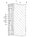
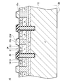
- the semiconductor device 10 of the embodiment shown in FIG. A plurality of trenches 14 are formed on the upper surface 12 a of the semiconductor substrate 12. The inner surface of each trench 14 is covered with a gate insulating film 16. A gate electrode 18 is disposed in each trench 14. Each gate electrode 18 is insulated from the semiconductor substrate 12 by the gate insulating film 16. The upper surface of each gate electrode 18 is covered with an interlayer insulating film 20. Each interlayer insulating film 20 is formed so as to protrude upward from the upper surface 12 a of the semiconductor substrate 12.
- a source electrode 22 is formed on the upper surface 12 a of the semiconductor substrate 12.
- the source electrode 22 covers the interlayer insulating film 20.
- the source electrode 22 is insulated from the gate electrode 18 by the interlayer insulating film 20.
- the source electrode 22 includes a buried electrode 22a, a Schottky electrode 22b, and a surface electrode 22c.
- a plurality of Schottky electrodes 22 b are formed on the semiconductor substrate 12. Each Schottky electrode 22b is disposed within a range sandwiched between two interlayer insulating films 20 and at a position separated from each interlayer insulating film 20. The Schottky electrode 22 b is formed so as to protrude upward from the upper surface 12 a of the semiconductor substrate 12. The height from the upper surface 12 a of the semiconductor substrate 12 to the upper surface of the Schottky electrode 22 b is substantially equal to the height from the upper surface 12 a of the semiconductor substrate 12 to the upper surface of the interlayer insulating film 20.
- the Schottky electrode 22b is made of Al (aluminum). The Schottky electrode 22 b is in Schottky contact with the semiconductor substrate 12.
- a recess 24 is formed between the interlayer insulating film 20 and the Schottky electrode 22b.
- the bottom surface of the recess 24 is the upper surface 12a of the semiconductor substrate 12, one side surface of the recess 24 is a side surface of the interlayer insulating film 20, and the other side surface of the recess 24 is a side surface of the Schottky electrode 22b.
- An angle ⁇ 1 between the bottom surface of the recess 24 (that is, the upper surface 12a of the semiconductor substrate 12) and the side surface of the interlayer insulating film 20 is greater than 90 degrees.
- the angle ⁇ 2 between the bottom surface of the recess 24 (that is, the upper surface 12a of the semiconductor substrate 12) and the side surface of the Schottky electrode 22b is greater than 90 degrees.
- the embedded electrode 22 a is disposed in each recess 24.
- the embedded electrode 22a is formed in the recess 24 without a gap.
- the embedded electrode 22a is in contact with the upper surface 12a of the semiconductor substrate 12 constituting the inner surface of the recess 24, the side surface of the interlayer insulating film 20, and the side surface of the Schottky electrode 22b.
- the embedded electrode 22a is made of W (tungsten).
- the embedded electrode 22 a is in ohmic contact with the semiconductor substrate 12.
- the surface electrode 22c is formed on the interlayer insulating film 20, the buried electrode 22a, and the Schottky electrode 22b.
- the surface electrode 22c extends over the interlayer insulating film 20, the buried electrode 22a, and the Schottky electrode 22b.
- the surface electrode 22c is made of Al.
- the surface electrode 22c is made of the same material as the Schottky electrode 22b. Therefore, in this embodiment, it is difficult to visually recognize the boundary between the surface electrode 22c and the Schottky electrode 22b. However, even when the boundary cannot be visually recognized, the Al layer positioned on the side of the embedded electrode 22a can be recognized as the Schottky electrode 22b, and the Al layer positioned above the upper surface of the embedded electrode 22a can be recognized as the surface electrode 22c. .
- a drain electrode 26 is formed on the lower surface 12 b of the semiconductor substrate 12.
- the drain electrode 26 is in ohmic contact with the semiconductor substrate 12.
- a source region 30, an upper body region 32, an intermediate region 34, a lower body region 36, a drift region 38, and a drain region 40 are formed inside the semiconductor substrate 12.
- the source region 30 is an n-type semiconductor region.
- the source region 30 is exposed on the upper surface 12 a of the semiconductor substrate 12.
- the source region 30 is in ohmic contact with the buried electrode 22a.
- the source region 30 is in contact with the gate insulating film 16.
- the upper body region 32 is formed on the side and the lower side of the source region 30.
- the upper body region 32 includes a high concentration region 32a that is a p-type semiconductor region having a high p-type impurity concentration, and a low concentration region 32b that is a p-type semiconductor region having a p-type impurity concentration lower than that of the high concentration region 32a. is doing.
- the high concentration region 32 a is formed on the side of the source region 30 and is exposed on the upper surface 12 a of the semiconductor substrate 12.
- the high concentration region 32a is in ohmic contact with the embedded electrode 22a.
- the low concentration region 32b is formed below the source region 30 and the high concentration region 32a.
- the low concentration region 32 b is in contact with the gate insulating film 16 below the source region 30.
- the intermediate region 34 is an n-type semiconductor region having a relatively low n-type impurity concentration.
- the intermediate region 34 is in contact with the upper body region 32.
- the intermediate region 34 is separated from the source region 30 by the upper body region 32.
- the intermediate region 34 has a pillar region 34a and a barrier region 34b.
- the pillar region 34 a is a region extending from the upper surface 12 a of the semiconductor substrate 12 along the thickness direction of the semiconductor substrate 12.
- the pillar region 34a is exposed on the upper surface 12a of the semiconductor substrate 12, and is in Schottky contact with the Schottky electrode 22b.
- the barrier region 34 b is formed below the upper body region 32.
- the barrier region 34b is connected to the pillar region 34a.
- the barrier region 34 b is in contact with the gate insulating film 16 below the upper body region 32.
- the lower body region 36 is a p-type semiconductor region.
- the lower body region 36 is formed below the intermediate region 34.
- the lower body region 36 is in contact with the gate insulating film 16 below the barrier region 34b.
- the lower body region 36 is separated from the upper body region 32 by the intermediate region 34.
- the drift region 38 is an n-type semiconductor region having a relatively low n-type impurity concentration.
- the drift region 38 is formed below the lower body region 36.
- the drift region 38 is in contact with the gate insulating film 16 below the lower body region 36.
- the drift region 38 is separated from the intermediate region 34 by the lower body region 36.
- the drain region 40 is an n-type semiconductor region having an n-type impurity concentration higher than that of the drift region 38.
- the drain region 40 is formed below the drift region 38.
- the drain region 40 is exposed on the lower surface 12 b of the semiconductor substrate 12.
- the drain region 40 is in ohmic contact with the drain electrode 26.
- the semiconductor device 10 can perform an operation as a MOSFET and an operation as a diode.
- a higher potential than the source electrode 22 is applied to the drain electrode 26.
- a potential higher than the threshold value is applied to the gate electrode 18 to the gate electrode 18.
- a current flows from the drain electrode 26 toward the source electrode 22 through the drain region 40, the drift region 38, the channel of the lower body region 36, the intermediate region 34, the channel of the upper body region 32 and the source region 30. . That is, the MOSFET is turned on.
- the potential of the gate electrode 18 is lowered below the threshold value, the channel disappears and the current stops.
- a Schottky diode having a Schottky interface that is a boundary between the source electrode 22 and the intermediate region 34 and a pn junction that is a boundary between the upper body region 32 and the intermediate region 34 are provided between the source electrode 22 and the drain electrode 26 .
- a pn diode is formed.
- the semiconductor device 10 operates as a diode, a potential higher than that of the drain electrode 26 is applied to the source electrode 22. Then, the Schottky interface at the boundary between the source electrode 22 and the intermediate region 34 is turned on. As a result, a current flows from the source electrode 22 toward the drain electrode 26 via the intermediate region 34, the lower body region 36, the drift region 38 and the drain region 40.
- the potential of the barrier region 34 b is set to a potential substantially equal to the potential of the source electrode 22. This makes it difficult for the pn junction at the boundary between the upper body region 32 and the intermediate region 34 to be turned on, and suppresses holes from flowing into the drift region 38 from the upper body region 32. Thereafter, when a reverse voltage is applied to the diode, the diode performs a reverse recovery operation. Since the inflow of holes into the drift region 38 is suppressed when the diode is on as described above, the reverse current flowing through the diode during the reverse recovery operation is suppressed.
- the semiconductor device 10 is manufactured from an n-type semiconductor substrate 12 having substantially the same impurity concentration as the drift region 38.
- the source region 30, the upper body region 32, the intermediate region 34, and the lower body region 36 are formed in the semiconductor substrate 12 by ion implantation or the like.
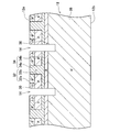
- the upper surface 12a of the semiconductor substrate 12 is selectively etched to form trenches 14 in the upper surface 12a of the semiconductor substrate 12, as shown in FIG.
- the trench 14 is formed so as to penetrate the source region 30, the low concentration region 32b, the barrier region 34b, and the lower body region 36.
- a gate insulating film 16 is formed on the inner surface of the trench 14.
- the gate electrode 18 is formed inside the trench 14.
- the semiconductor substrate 12 and the electrodes, insulating layers, and the like formed on the semiconductor substrate 12 are collectively referred to as a wafer 13.
- an interlayer insulating film 20 is grown on the wafer 13.
- the interlayer insulating film 20 is formed so as to cover the entire upper surface of the wafer 13.
- the interlayer insulating film 20 is selectively etched.
- the interlayer insulating film 20 is left on the gate electrode 18 and the interlayer insulating film 20 at other positions is removed.
- the interlayer insulating film 20 is formed so that the angle ⁇ ⁇ b> 1 between the side surface of the interlayer insulating film 20 and the exposed upper surface 12 a of the semiconductor substrate 12 is greater than 90 degrees. Sides are molded.
- a Schottky electrode 22b (ie, Al) is grown on the wafer 13 by sputtering.
- the Schottky electrode 22 b is formed so as to cover the entire upper surface 12 a of the semiconductor substrate 12 and the entire surface of the interlayer insulating film 20.
- the Schottky electrode 22b is selectively etched. As a result, as shown in FIG. 8, the Schottky electrode 22b is left in the range where the intermediate region 34 is exposed on the upper surface 12a, and the Schottky electrode 22b at other positions is removed.
- FIG. 8 the Schottky electrode 22b
- the Schottky electrode 22 b has an angle ⁇ 2 larger than 90 degrees between the side surface of the Schottky electrode 22 b and the exposed upper surface 12 a of the semiconductor substrate 12. Sides are molded. By thus etching the Schottky electrode 22b, the Schottky electrode 22b is separated from the interlayer insulating film 20. Therefore, a recess 24 is formed between the Schottky electrode 22b and the interlayer insulating film 20.
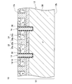
- a buried electrode 22a (ie, W) is grown on the wafer 13.
- the embedded electrode 22a is formed so as to cover the entire upper surface 12a of the semiconductor substrate 12, the interlayer insulating film 20, and the entire surface of the Schottky electrode 22b.
- W which is the material of the embedded electrode 22a grows evenly on the surface of the base material. For this reason, as shown in FIG. 9, even if the surface of the wafer 13 is uneven due to the interlayer insulating film 20 and the Schottky electrode 22b, the surface of the embedded electrode 22a becomes substantially flat. Further, W, which is the material of the embedded electrode 22a, can be grown in the narrow recess 24 without any gap.
- the angle ⁇ 1 between the bottom surface and the side surface on the interlayer insulating film 20 side is larger than 90 degrees
- the angle ⁇ 2 between the bottom surface and the side surface on the Schottky electrode 22b side is larger than 90 degrees. That is, the recess 24 has a width at the upper end that is wider than that at the bottom. For this reason, the embedded electrode 22 a can be reliably grown in the recess 24. Accordingly, the formation of a gap in the recess 24 is prevented.
- the embedded electrode 22a is etched.
- SF6 sulfur hexafluoride
- the upper surface of the buried electrode 22a is retreated to the lower side from the upper surface of the interlayer insulating film 20 and the upper surface of the Schottky electrode 22b by etching. That is, the upper surface of the interlayer insulating film 20 and the upper surface of the Schottky electrode 22b are exposed. For this reason, the interlayer insulating film 20 remains in the recess 24.
- the etching time is adjusted so that the upper surface of the buried electrode 22a after the etching becomes a height close to the upper surface of the interlayer insulating film 20 and the upper surface of the Schottky electrode 22b. Further, when the embedded electrode 22a is etched in this way, the upper surface of the embedded electrode 22a becomes substantially flat. The reason will be described below.
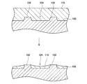
- FIGS. 11 and 12 are explanatory views of a process for etching a metal.
- the metal layer 110 is formed on the surface 100 having the two convex portions 102 and the concave portion 104 sandwiched between the two convex portions 102, and then the upper surface of the two convex portions 102 is exposed.
- the process of etching the metal layer 110 is shown.
- FIG. 11 shows a case where the width of the recess 104 is wide
- FIG. 12 shows a case where the width of the recess 104 is narrow. Etching proceeds faster at the center of the recess 104 than at the end of the recess 104 (ie, near the protrusion 102).
- a convex Schottky electrode 22b is formed at a position spaced from the convex interlayer insulating film 20.
- a narrow recess 24 is formed between the interlayer insulating film 20 and the Schottky electrode 22b.
- the upper surface of the embedded electrode 22a can be made substantially flat after the embedded electrode 22a is etched. For this reason, after the etching of the embedded electrode 22a, the upper surface of the wafer 13 constituted by the upper surface of the embedded electrode 22a, the upper surface of the interlayer insulating film 20, and the upper surface of the Schottky electrode 22b becomes substantially flat.
- the surface electrode 22 c (that is, Al) is grown on the wafer 13.
- the surface electrode 22c is formed so as to cover the entire upper surface of the interlayer insulating film 20, the buried electrode 22a, and the Schottky electrode 22b. As described above, since the upper surface of the wafer 13 is flat, the upper surface of the surface electrode 22c is flat.
- the back side structure that is, the drain region 40 and the drain electrode 26
- the wafer 13 is diced to complete the semiconductor device 10 shown in FIG.
- the surface of the surface electrode 22c can be planarized.
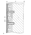
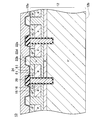
- the source electrode 22 has a barrier metal layer 22d.
- Other configurations of the semiconductor device 200 of the second embodiment are the same as those of the semiconductor device 10 of the first embodiment.
- the barrier metal layer 22d is made of TiN (titanium nitride). The thickness of the barrier metal layer 22d is much thinner than the interlayer insulating film 20 and the Schottky electrode 22b. The barrier metal layer 22 d covers the upper surface of the interlayer insulating film 20, the upper surface of the Schottky electrode 22 b, and the inner surface of the recess 24.
- the semiconductor device 200 according to the second embodiment operates in substantially the same manner as the semiconductor device 10 according to the first embodiment.
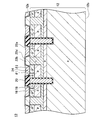
- the wafer 13 is processed as shown in FIG.
- a barrier metal layer 22 d is grown on the wafer 13. That is, the barrier metal layer 22 d is grown on the upper surface of the interlayer insulating film 20, the upper surface of the Schottky electrode 22 b, and the inner surface of the recess 24. That is, in Example 2, the convex portion on the gate electrode 18 is constituted by the interlayer insulating film 20 and the barrier metal layer 22d. Further, the convex portion on the pillar region 34a is constituted by the Schottky electrode 22b and the barrier metal layer 22d.
- a buried electrode 22a ie, W
- the surface of the embedded electrode 22a becomes flat, and the embedded electrode 22a is formed in the recess 24 without any gap.
- the embedded electrode 22a is etched.
- SF6 sulfur hexafluoride
- the upper surface of the buried electrode 22a is made to recede below the upper surface of the barrier metal layer 22d on the interlayer insulating film 20 and the upper surface of the barrier metal layer 22d on the Schottky electrode 22b. That is, the barrier metal layer 22d on the interlayer insulating film 20 and the Schottky electrode 22b is exposed.
- the embedded electrode 22a is left in the recess 24.
- the interlayer insulating film 20 and the Schottky electrode 22b are covered with the barrier metal layer 22d, the interlayer insulating film 20 and the Schottky electrode 22b are not exposed to the etching gas during the etching shown in FIG.
- the selection ratio of the barrier metal layer 22d (TiN) and the embedded electrode 22a (W) to be etched to the etching gas (SF6) is 1:30. That is, the barrier metal layer 22d is hardly etched by the etching gas. Therefore, the interlayer insulating film 20 and the Schottky electrode 22b are protected from the etching gas by the barrier metal layer 22d.
- a material having at least the above selection ratio of 1: 5 can be used as the barrier metal layer 22d.
- the upper surface of the wafer 13 becomes substantially flat after the etching of the embedded electrode 22a.
- a surface electrode 22c is grown on the upper surface of the wafer 13, as shown in FIG. Similar to the first embodiment, the surface electrode 22c having a flat upper surface can be formed. Thereafter, the structure on the lower surface side is formed and diced to complete the semiconductor device 200 shown in FIG.
- the surface of the surface electrode 22c can be planarized also in the manufacturing process of the semiconductor device 200 of the second embodiment. Further, according to the method of the second embodiment, the interlayer insulating film 20 and the Schottky electrode 22b can be protected from the etching gas.
- the semiconductor device having the MOSFET having the trench gate electrode and the Schottky diode has been described.
- an IGBT having a trench-type gate electrode may be formed instead of the MOSFET.
- a pn diode having electrodes arranged in the trench may be formed instead of the MOSFET. That is, the technique disclosed in this specification can be applied to various semiconductor devices including an element having an electrode arranged in a trench and a Schottky electrode.
- the Schottky electrode 22b and the surface electrode 22c are made of the same Al, but they may be made of different materials.
- the Schottky electrode 22b may be made of Pd (palladium).
- the angle between the surface of the semiconductor substrate and the side surface of the interlayer insulating film is greater than 90 degrees within a range covered with the buried electrode.
- the embedded electrode can be suitably formed in the recess.
- the angle between the surface of the semiconductor substrate and the side surface of the Schottky electrode is greater than 90 degrees within a range covered with the embedded electrode.
- the embedded electrode can be suitably formed in the recess.
- a barrier metal layer having etching selectivity with respect to a buried electrode is disposed between a Schottky electrode and a surface electrode and between an interlayer insulating film and a surface electrode. ing.
- the Schottky electrode and the interlayer insulating film can be protected from the etching agent.
- the embedded electrode is in ohmic contact with the semiconductor substrate.
- the embedded electrode is made of a metal different from the Schottky electrode.
Landscapes
- Engineering & Computer Science (AREA)
- Physics & Mathematics (AREA)
- Condensed Matter Physics & Semiconductors (AREA)
- General Physics & Mathematics (AREA)
- Manufacturing & Machinery (AREA)
- Computer Hardware Design (AREA)
- Microelectronics & Electronic Packaging (AREA)
- Power Engineering (AREA)
- Electrodes Of Semiconductors (AREA)
- Metal-Oxide And Bipolar Metal-Oxide Semiconductor Integrated Circuits (AREA)
Priority Applications (4)
| Application Number | Priority Date | Filing Date | Title |
|---|---|---|---|
| DE112015003835.3T DE112015003835B4 (de) | 2014-08-22 | 2015-06-23 | Halbleitervorrichtung und verfahren zur herstellung der halbleitervorrichtung |
| KR1020167031726A KR101868730B1 (ko) | 2014-08-22 | 2015-06-23 | 반도체 장치 및 반도체 장치의 제조 방법 |
| CN201580045037.9A CN106575668B (zh) | 2014-08-22 | 2015-06-23 | 半导体装置以及半导体装置的制造方法 |
| US15/125,857 US9941273B2 (en) | 2014-08-22 | 2015-06-23 | Semiconductor device and method of manufacturing the semiconductor device |
Applications Claiming Priority (2)
| Application Number | Priority Date | Filing Date | Title |
|---|---|---|---|
| JP2014169454A JP6036765B2 (ja) | 2014-08-22 | 2014-08-22 | 半導体装置及び半導体装置の製造方法 |
| JP2014-169454 | 2014-08-22 |
Publications (1)
| Publication Number | Publication Date |
|---|---|
| WO2016027564A1 true WO2016027564A1 (ja) | 2016-02-25 |
Family
ID=55350516
Family Applications (1)
| Application Number | Title | Priority Date | Filing Date |
|---|---|---|---|
| PCT/JP2015/068095 WO2016027564A1 (ja) | 2014-08-22 | 2015-06-23 | 半導体装置及び半導体装置の製造方法 |
Country Status (7)
Cited By (2)
| Publication number | Priority date | Publication date | Assignee | Title |
|---|---|---|---|---|
| JP2018022836A (ja) * | 2016-08-05 | 2018-02-08 | トヨタ自動車株式会社 | 半導体装置 |
| CN117012830A (zh) * | 2023-08-18 | 2023-11-07 | 广微集成技术(深圳)有限公司 | 一种屏蔽栅沟槽vdmos器件及其制造方法 |
Families Citing this family (9)
| Publication number | Priority date | Publication date | Assignee | Title |
|---|---|---|---|---|
| JP6299789B2 (ja) * | 2016-03-09 | 2018-03-28 | トヨタ自動車株式会社 | スイッチング素子 |
| JP6784164B2 (ja) * | 2016-12-15 | 2020-11-11 | 株式会社豊田中央研究所 | 半導体装置 |
| DE102017118665A1 (de) * | 2017-08-16 | 2019-02-21 | Infineon Technologies Ag | Rc-igbt |
| JP6776205B2 (ja) * | 2017-09-20 | 2020-10-28 | 株式会社東芝 | 半導体装置の製造方法 |
| JP6861855B2 (ja) * | 2018-02-02 | 2021-04-21 | 三菱電機株式会社 | 半導体装置の製造方法 |
| JP6964538B2 (ja) | 2018-02-28 | 2021-11-10 | 株式会社 日立パワーデバイス | 半導体装置および電力変換装置 |
| US11417762B2 (en) | 2019-06-26 | 2022-08-16 | Skyworks Solutions, Inc. | Switch with integrated Schottky barrier contact |
| DE102021104532B4 (de) * | 2021-02-25 | 2025-06-18 | Infineon Technologies Ag | Mesa-Kontakt für MOS-gesteuerte Leistungshalbleitervorrichtung undVerfahren zum Herstellen einer Leistungshalbleitervorrichtung |
| CN113921614B (zh) * | 2021-12-13 | 2022-03-25 | 捷捷微电(上海)科技有限公司 | 一种半导体功率器件结构及其制造方法 |
Citations (4)
| Publication number | Priority date | Publication date | Assignee | Title |
|---|---|---|---|---|
| JP2005101514A (ja) * | 2003-08-27 | 2005-04-14 | Mitsubishi Electric Corp | 絶縁ゲート型トランジスタ及びインバータ回路 |
| JP2011091283A (ja) * | 2009-10-26 | 2011-05-06 | Mitsubishi Electric Corp | 半導体装置およびその製造方法 |
| JP2011199060A (ja) * | 2010-03-19 | 2011-10-06 | Toshiba Corp | 半導体装置及びその製造方法 |
| US20140231827A1 (en) * | 2013-02-15 | 2014-08-21 | Denso Corporation | Semiconductor device and manufacturing method thereof |
Family Cites Families (14)
| Publication number | Priority date | Publication date | Assignee | Title |
|---|---|---|---|---|
| US6593620B1 (en) * | 2000-10-06 | 2003-07-15 | General Semiconductor, Inc. | Trench DMOS transistor with embedded trench schottky rectifier |
| US6998678B2 (en) * | 2001-05-17 | 2006-02-14 | Infineon Technologies Ag | Semiconductor arrangement with a MOS-transistor and a parallel Schottky-diode |
| EP1552562A1 (en) * | 2002-10-04 | 2005-07-13 | Koninklijke Philips Electronics N.V. | Power semiconductor devices |
| JP4406535B2 (ja) * | 2003-01-14 | 2010-01-27 | 新電元工業株式会社 | ショットキーダイオード付きトランジスタ |
| JP4829473B2 (ja) | 2004-01-21 | 2011-12-07 | オンセミコンダクター・トレーディング・リミテッド | 絶縁ゲート型半導体装置およびその製造方法 |
| JP4935160B2 (ja) * | 2006-04-11 | 2012-05-23 | 株式会社デンソー | 炭化珪素半導体装置およびその製造方法 |
| JP4292427B2 (ja) * | 2006-12-04 | 2009-07-08 | サンケン電気株式会社 | 絶縁ゲート型電界効果トランジスタ及びその製造方法 |
| US8049276B2 (en) * | 2009-06-12 | 2011-11-01 | Fairchild Semiconductor Corporation | Reduced process sensitivity of electrode-semiconductor rectifiers |
| EP2565922B1 (en) * | 2010-04-28 | 2020-04-01 | Nissan Motor Co., Ltd | Semiconductor device |
| US8580667B2 (en) * | 2010-12-14 | 2013-11-12 | Alpha And Omega Semiconductor Incorporated | Self aligned trench MOSFET with integrated diode |
| CN103890955B (zh) | 2011-07-27 | 2017-06-13 | 丰田自动车株式会社 | 半导体器件 |
| DE112012005869B4 (de) * | 2012-02-14 | 2021-09-23 | Denso Corporation | IGBT und IGBT-Herstellungsverfahren |
| US8809948B1 (en) * | 2012-12-21 | 2014-08-19 | Alpha And Omega Semiconductor Incorporated | Device structure and methods of making high density MOSFETs for load switch and DC-DC applications |
| US8951867B2 (en) * | 2012-12-21 | 2015-02-10 | Alpha And Omega Semiconductor Incorporated | High density trench-based power MOSFETs with self-aligned active contacts and method for making such devices |
-
2014
- 2014-08-22 JP JP2014169454A patent/JP6036765B2/ja active Active
-
2015
- 2015-06-23 US US15/125,857 patent/US9941273B2/en active Active
- 2015-06-23 CN CN201580045037.9A patent/CN106575668B/zh not_active Expired - Fee Related
- 2015-06-23 DE DE112015003835.3T patent/DE112015003835B4/de not_active Expired - Fee Related
- 2015-06-23 KR KR1020167031726A patent/KR101868730B1/ko not_active Expired - Fee Related
- 2015-06-23 WO PCT/JP2015/068095 patent/WO2016027564A1/ja active Application Filing
- 2015-08-11 TW TW104126111A patent/TWI587478B/zh not_active IP Right Cessation
Patent Citations (4)
| Publication number | Priority date | Publication date | Assignee | Title |
|---|---|---|---|---|
| JP2005101514A (ja) * | 2003-08-27 | 2005-04-14 | Mitsubishi Electric Corp | 絶縁ゲート型トランジスタ及びインバータ回路 |
| JP2011091283A (ja) * | 2009-10-26 | 2011-05-06 | Mitsubishi Electric Corp | 半導体装置およびその製造方法 |
| JP2011199060A (ja) * | 2010-03-19 | 2011-10-06 | Toshiba Corp | 半導体装置及びその製造方法 |
| US20140231827A1 (en) * | 2013-02-15 | 2014-08-21 | Denso Corporation | Semiconductor device and manufacturing method thereof |
Cited By (2)
| Publication number | Priority date | Publication date | Assignee | Title |
|---|---|---|---|---|
| JP2018022836A (ja) * | 2016-08-05 | 2018-02-08 | トヨタ自動車株式会社 | 半導体装置 |
| CN117012830A (zh) * | 2023-08-18 | 2023-11-07 | 广微集成技术(深圳)有限公司 | 一种屏蔽栅沟槽vdmos器件及其制造方法 |
Also Published As
| Publication number | Publication date |
|---|---|
| JP2016046377A (ja) | 2016-04-04 |
| CN106575668B (zh) | 2019-09-03 |
| KR20160138308A (ko) | 2016-12-02 |
| TWI587478B (zh) | 2017-06-11 |
| TW201624670A (zh) | 2016-07-01 |
| US20170040316A1 (en) | 2017-02-09 |
| JP6036765B2 (ja) | 2016-11-30 |
| CN106575668A (zh) | 2017-04-19 |
| US9941273B2 (en) | 2018-04-10 |
| DE112015003835T5 (de) | 2017-05-11 |
| DE112015003835B4 (de) | 2020-10-15 |
| KR101868730B1 (ko) | 2018-06-18 |
Similar Documents
| Publication | Publication Date | Title |
|---|---|---|
| JP6036765B2 (ja) | 半導体装置及び半導体装置の製造方法 | |
| US8587054B2 (en) | Trench MOSFET with resurf stepped oxide and diffused drift region | |
| US9673279B2 (en) | Semiconductor device having multi-channel and method of forming the same | |
| US8901573B2 (en) | Silicon carbide semiconductor device and method of manufacturing the same | |
| TWI609488B (zh) | 具有場板的半導體元件 | |
| US8829607B1 (en) | Fast switching super-junction trench MOSFETs | |
| US20210028305A1 (en) | Trench mosfets with oxide charge balance region in active area and junction charge balance region in termination area | |
| US7989884B2 (en) | Structure for making a top-side contact to a substrate | |
| EP2998999A1 (en) | Semiconductor device | |
| JP6193163B2 (ja) | 絶縁ゲート型半導体装置 | |
| US11222962B2 (en) | Edge termination designs for super junction device | |
| US9947574B2 (en) | Semiconductor device | |
| JP7051890B2 (ja) | ワイドギャップ半導体装置 | |
| JP5556863B2 (ja) | ワイドバンドギャップ半導体縦型mosfet | |
| WO2015056318A1 (ja) | 炭化珪素半導体装置 | |
| JP7159949B2 (ja) | 半導体装置 | |
| US9530881B2 (en) | Semiconductor device, and method of manufacturing the same | |
| JP7371724B2 (ja) | 半導体装置とその製造方法 | |
| CN111406323B (zh) | 宽带隙半导体装置 | |
| US20130161635A1 (en) | Method and system for a gan self-aligned vertical mesfet | |
| JP6988262B2 (ja) | 窒化物半導体装置とその製造方法 | |
| JP6648743B2 (ja) | 炭化珪素半導体装置の製造方法 | |
| JP2019036606A (ja) | 窒化物半導体装置の製造方法 | |
| JP6680161B2 (ja) | スイッチング素子の製造方法 | |
| WO2018066662A1 (ja) | 炭化珪素半導体装置の製造方法 |
Legal Events
| Date | Code | Title | Description |
|---|---|---|---|
| 121 | Ep: the epo has been informed by wipo that ep was designated in this application |
Ref document number: 15833079 Country of ref document: EP Kind code of ref document: A1 |
|
| WWE | Wipo information: entry into national phase |
Ref document number: 15125857 Country of ref document: US |
|
| ENP | Entry into the national phase |
Ref document number: 20167031726 Country of ref document: KR Kind code of ref document: A |
|
| WWE | Wipo information: entry into national phase |
Ref document number: 112015003835 Country of ref document: DE |
|
| 122 | Ep: pct application non-entry in european phase |
Ref document number: 15833079 Country of ref document: EP Kind code of ref document: A1 |