WO2016013471A1 - 半導体装置及び半導体装置の製造方法 - Google Patents
半導体装置及び半導体装置の製造方法 Download PDFInfo
- Publication number
- WO2016013471A1 WO2016013471A1 PCT/JP2015/070336 JP2015070336W WO2016013471A1 WO 2016013471 A1 WO2016013471 A1 WO 2016013471A1 JP 2015070336 W JP2015070336 W JP 2015070336W WO 2016013471 A1 WO2016013471 A1 WO 2016013471A1
- Authority
- WO
- WIPO (PCT)
- Prior art keywords
- region
- semiconductor
- insulating film
- conductivity type
- semiconductor substrate
- Prior art date
- Legal status (The legal status is an assumption and is not a legal conclusion. Google has not performed a legal analysis and makes no representation as to the accuracy of the status listed.)
- Ceased
Links
Images



Classifications
-
- H—ELECTRICITY
- H10—SEMICONDUCTOR DEVICES; ELECTRIC SOLID-STATE DEVICES NOT OTHERWISE PROVIDED FOR
- H10D—INORGANIC ELECTRIC SEMICONDUCTOR DEVICES
- H10D30/00—Field-effect transistors [FET]
- H10D30/60—Insulated-gate field-effect transistors [IGFET]
- H10D30/64—Double-diffused metal-oxide semiconductor [DMOS] FETs
- H10D30/66—Vertical DMOS [VDMOS] FETs
- H10D30/665—Vertical DMOS [VDMOS] FETs having edge termination structures
-
- H—ELECTRICITY
- H10—SEMICONDUCTOR DEVICES; ELECTRIC SOLID-STATE DEVICES NOT OTHERWISE PROVIDED FOR
- H10D—INORGANIC ELECTRIC SEMICONDUCTOR DEVICES
- H10D12/00—Bipolar devices controlled by the field effect, e.g. insulated-gate bipolar transistors [IGBT]
- H10D12/01—Manufacture or treatment
- H10D12/031—Manufacture or treatment of IGBTs
-
- H—ELECTRICITY
- H10—SEMICONDUCTOR DEVICES; ELECTRIC SOLID-STATE DEVICES NOT OTHERWISE PROVIDED FOR
- H10D—INORGANIC ELECTRIC SEMICONDUCTOR DEVICES
- H10D30/00—Field-effect transistors [FET]
- H10D30/01—Manufacture or treatment
- H10D30/021—Manufacture or treatment of FETs having insulated gates [IGFET]
- H10D30/028—Manufacture or treatment of FETs having insulated gates [IGFET] of double-diffused metal oxide semiconductor [DMOS] FETs
- H10D30/0291—Manufacture or treatment of FETs having insulated gates [IGFET] of double-diffused metal oxide semiconductor [DMOS] FETs of vertical DMOS [VDMOS] FETs
-
- H—ELECTRICITY
- H10—SEMICONDUCTOR DEVICES; ELECTRIC SOLID-STATE DEVICES NOT OTHERWISE PROVIDED FOR
- H10D—INORGANIC ELECTRIC SEMICONDUCTOR DEVICES
- H10D30/00—Field-effect transistors [FET]
- H10D30/60—Insulated-gate field-effect transistors [IGFET]
- H10D30/64—Double-diffused metal-oxide semiconductor [DMOS] FETs
- H10D30/66—Vertical DMOS [VDMOS] FETs
- H10D30/662—Vertical DMOS [VDMOS] FETs having a drift region having a doping concentration that is higher between adjacent body regions relative to other parts of the drift region
-
- H—ELECTRICITY
- H10—SEMICONDUCTOR DEVICES; ELECTRIC SOLID-STATE DEVICES NOT OTHERWISE PROVIDED FOR
- H10D—INORGANIC ELECTRIC SEMICONDUCTOR DEVICES
- H10D62/00—Semiconductor bodies, or regions thereof, of devices having potential barriers
- H10D62/10—Shapes, relative sizes or dispositions of the regions of the semiconductor bodies; Shapes of the semiconductor bodies
- H10D62/13—Semiconductor regions connected to electrodes carrying current to be rectified, amplified or switched, e.g. source or drain regions
- H10D62/149—Source or drain regions of field-effect devices
- H10D62/151—Source or drain regions of field-effect devices of IGFETs
- H10D62/156—Drain regions of DMOS transistors
- H10D62/157—Impurity concentrations or distributions
-
- H—ELECTRICITY
- H10—SEMICONDUCTOR DEVICES; ELECTRIC SOLID-STATE DEVICES NOT OTHERWISE PROVIDED FOR
- H10D—INORGANIC ELECTRIC SEMICONDUCTOR DEVICES
- H10D62/00—Semiconductor bodies, or regions thereof, of devices having potential barriers
- H10D62/10—Shapes, relative sizes or dispositions of the regions of the semiconductor bodies; Shapes of the semiconductor bodies
- H10D62/17—Semiconductor regions connected to electrodes not carrying current to be rectified, amplified or switched, e.g. channel regions
- H10D62/393—Body regions of DMOS transistors or IGBTs
-
- H—ELECTRICITY
- H10—SEMICONDUCTOR DEVICES; ELECTRIC SOLID-STATE DEVICES NOT OTHERWISE PROVIDED FOR
- H10D—INORGANIC ELECTRIC SEMICONDUCTOR DEVICES
- H10D62/00—Semiconductor bodies, or regions thereof, of devices having potential barriers
- H10D62/80—Semiconductor bodies, or regions thereof, of devices having potential barriers characterised by the materials
- H10D62/83—Semiconductor bodies, or regions thereof, of devices having potential barriers characterised by the materials being Group IV materials, e.g. B-doped Si or undoped Ge
- H10D62/832—Semiconductor bodies, or regions thereof, of devices having potential barriers characterised by the materials being Group IV materials, e.g. B-doped Si or undoped Ge being Group IV materials comprising two or more elements, e.g. SiGe
- H10D62/8325—Silicon carbide
-
- H—ELECTRICITY
- H10—SEMICONDUCTOR DEVICES; ELECTRIC SOLID-STATE DEVICES NOT OTHERWISE PROVIDED FOR
- H10D—INORGANIC ELECTRIC SEMICONDUCTOR DEVICES
- H10D64/00—Electrodes of devices having potential barriers
- H10D64/118—Electrodes comprising insulating layers having particular dielectric or electrostatic properties, e.g. having static charges
-
- H—ELECTRICITY
- H10—SEMICONDUCTOR DEVICES; ELECTRIC SOLID-STATE DEVICES NOT OTHERWISE PROVIDED FOR
- H10D—INORGANIC ELECTRIC SEMICONDUCTOR DEVICES
- H10D64/00—Electrodes of devices having potential barriers
- H10D64/20—Electrodes characterised by their shapes, relative sizes or dispositions
- H10D64/23—Electrodes carrying the current to be rectified, amplified, oscillated or switched, e.g. sources, drains, anodes or cathodes
- H10D64/251—Source or drain electrodes for field-effect devices
- H10D64/252—Source or drain electrodes for field-effect devices for vertical or pseudo-vertical devices
-
- H—ELECTRICITY
- H10—SEMICONDUCTOR DEVICES; ELECTRIC SOLID-STATE DEVICES NOT OTHERWISE PROVIDED FOR
- H10D—INORGANIC ELECTRIC SEMICONDUCTOR DEVICES
- H10D64/00—Electrodes of devices having potential barriers
- H10D64/20—Electrodes characterised by their shapes, relative sizes or dispositions
- H10D64/23—Electrodes carrying the current to be rectified, amplified, oscillated or switched, e.g. sources, drains, anodes or cathodes
- H10D64/251—Source or drain electrodes for field-effect devices
- H10D64/258—Source or drain electrodes for field-effect devices characterised by the relative positions of the source or drain electrodes with respect to the gate electrode
-
- H—ELECTRICITY
- H10—SEMICONDUCTOR DEVICES; ELECTRIC SOLID-STATE DEVICES NOT OTHERWISE PROVIDED FOR
- H10D—INORGANIC ELECTRIC SEMICONDUCTOR DEVICES
- H10D30/00—Field-effect transistors [FET]
- H10D30/60—Insulated-gate field-effect transistors [IGFET]
- H10D30/64—Double-diffused metal-oxide semiconductor [DMOS] FETs
- H10D30/66—Vertical DMOS [VDMOS] FETs
- H10D30/669—Vertical DMOS [VDMOS] FETs having voltage-sensing or current-sensing structures, e.g. emulator sections or overcurrent sensing cells
-
- H—ELECTRICITY
- H10—SEMICONDUCTOR DEVICES; ELECTRIC SOLID-STATE DEVICES NOT OTHERWISE PROVIDED FOR
- H10D—INORGANIC ELECTRIC SEMICONDUCTOR DEVICES
- H10D62/00—Semiconductor bodies, or regions thereof, of devices having potential barriers
- H10D62/10—Shapes, relative sizes or dispositions of the regions of the semiconductor bodies; Shapes of the semiconductor bodies
- H10D62/102—Constructional design considerations for preventing surface leakage or controlling electric field concentration
- H10D62/103—Constructional design considerations for preventing surface leakage or controlling electric field concentration for increasing or controlling the breakdown voltage of reverse-biased devices
- H10D62/104—Constructional design considerations for preventing surface leakage or controlling electric field concentration for increasing or controlling the breakdown voltage of reverse-biased devices having particular shapes of the bodies at or near reverse-biased junctions, e.g. having bevels or moats
-
- H—ELECTRICITY
- H10—SEMICONDUCTOR DEVICES; ELECTRIC SOLID-STATE DEVICES NOT OTHERWISE PROVIDED FOR
- H10D—INORGANIC ELECTRIC SEMICONDUCTOR DEVICES
- H10D62/00—Semiconductor bodies, or regions thereof, of devices having potential barriers
- H10D62/10—Shapes, relative sizes or dispositions of the regions of the semiconductor bodies; Shapes of the semiconductor bodies
- H10D62/102—Constructional design considerations for preventing surface leakage or controlling electric field concentration
- H10D62/103—Constructional design considerations for preventing surface leakage or controlling electric field concentration for increasing or controlling the breakdown voltage of reverse-biased devices
- H10D62/105—Constructional design considerations for preventing surface leakage or controlling electric field concentration for increasing or controlling the breakdown voltage of reverse-biased devices by having particular doping profiles, shapes or arrangements of PN junctions; by having supplementary regions, e.g. junction termination extension [JTE]
-
- H—ELECTRICITY
- H10—SEMICONDUCTOR DEVICES; ELECTRIC SOLID-STATE DEVICES NOT OTHERWISE PROVIDED FOR
- H10D—INORGANIC ELECTRIC SEMICONDUCTOR DEVICES
- H10D62/00—Semiconductor bodies, or regions thereof, of devices having potential barriers
- H10D62/40—Crystalline structures
- H10D62/405—Orientations of crystalline planes
Definitions
- the present invention relates to a semiconductor device and a method for manufacturing the semiconductor device.
- MOSFET Metal Oxide Semiconductor Field-Effect Transistor
- SiC silicon carbide
- HTGB high temperature gate bias
- the threshold voltage is lowered by the diffusion of impurities from the outside.
- titanium (Ti) -based metal that prevents diffusion of impurities is formed on the surface of the MOSFET (for example, see Patent Document 1).
- SiN silicon nitride
- SiO 2 silicon oxide
- An object of the present invention is to provide a semiconductor device capable of suppressing a decrease in threshold voltage and suppressing deterioration of characteristics of the semiconductor device in order to solve the above-described problems caused by the prior art. It is another object of the present invention to provide a semiconductor device and a method for manufacturing the semiconductor device that can suppress an increase in the number of processes during manufacturing.
- the semiconductor device has the following characteristics.
- a semiconductor substrate made of silicon carbide of the first conductivity type is provided, and a first conductivity type semiconductor layer having an impurity concentration lower than that of the semiconductor substrate is provided on the first main surface of the semiconductor substrate.
- a base region of the second conductivity type is provided on the surface of the semiconductor layer, and a source region of the first conductivity type is provided in the surface region of the base region.
- a contact region of a second conductivity type having a higher impurity concentration than the base region is provided in a surface region of the base region, and includes a source electrode in contact with the source region and the contact region.
- a gate insulating film is provided on a surface of the base region between the semiconductor layer and the source region, and a gate electrode is provided on the surface of the gate insulating film.
- An interlayer insulating film is provided on the surface of the gate electrode, and a drain electrode is provided on the second main surface of the semiconductor substrate.
- the interlayer insulating film has a plurality of layers, and at least one of the plurality of layers is made of a silicon nitride film.
- the semiconductor device has the following features.
- a semiconductor substrate made of silicon carbide of the first conductivity type is provided, and a first conductivity type semiconductor layer having an impurity concentration lower than that of the semiconductor substrate is provided on the first main surface of the semiconductor substrate.
- a second conductivity type semiconductor region is provided in a part of the surface region of the semiconductor layer, and a second conductivity type base region having an impurity concentration lower than that of the semiconductor region is provided on the surface of the semiconductor region. .
- a well region made of silicon carbide of the first conductivity type having a lower impurity concentration than the semiconductor substrate is provided on the surface of the semiconductor layer in contact with the base region, and the well region is formed on the surface region of the base region from the well region.
- a first conductivity type source region having an impurity concentration higher than that of the well region is provided.
- a contact region of a second conductivity type having a higher impurity concentration than the base region is provided on the surface of the base region in contact with the source region, and includes a source electrode in contact with the source region and the contact region.
- a gate insulating film is provided on the surface of the base region between the well region and the source region, and a gate electrode is provided on the surface of the gate insulating film.
- An interlayer insulating film is provided on the surface of the gate electrode, and a drain electrode is provided on the second main surface of the semiconductor substrate.
- the interlayer insulating film has a plurality of layers, and at least one of the plurality of layers is made of a silicon nitride film.
- the layer made of the silicon nitride film in the interlayer insulating film is sandwiched between layers made of a silicon oxide film.
- the thickness of the layer made of the silicon nitride film is 0.2 ⁇ m or more.
- the layer made of the silicon oxide film above the layer made of the silicon nitride film in the interlayer insulating film is made of glass in which boron and phosphorus are added to silicon oxide.
- the layer made of the silicon nitride film in the interlayer insulating film is an uppermost layer.
- the thickness of the layer made of the silicon nitride film is 0.5 ⁇ m or more.
- the crystallographic plane index of the first main surface of the semiconductor substrate is a plane parallel to the (000-1) plane or a plane tilted within 10 degrees.
- the crystallographic plane index of the first main surface of the semiconductor substrate is a plane parallel to the (0001) plane or a plane tilted within 10 degrees.
- a method of manufacturing a semiconductor device comprising: a semiconductor substrate made of silicon carbide of a first conductivity type; and an impurity concentration lower than that of the semiconductor substrate provided on the first main surface of the semiconductor substrate.
- the method of manufacturing a semiconductor device and a drain electrode provided on the second major surface of said semiconductor substrate having the following features.
- the interlayer insulating film is formed of a plurality of layers, and at least one of the plurality of layers is formed of a silicon nitride film.
- a method of manufacturing a semiconductor device comprising: a semiconductor substrate made of silicon carbide of a first conductivity type; and an impurity concentration lower than that of the semiconductor substrate provided on the first main surface of the semiconductor substrate.
- a first conductivity type semiconductor layer ; a second conductivity type semiconductor region provided in a part of a surface region of the semiconductor layer; and an impurity concentration higher than that of the semiconductor region provided on the surface of the semiconductor region.
- the method for manufacturing a semiconductor device including the drain electrode provided on the semiconductor device has the following characteristics.
- the interlayer insulating film is formed of a plurality of layers, and at least one of the plurality of layers is formed of a silicon nitride film.
- the layer made of the silicon nitride film in the interlayer insulating film prevents the element causing the threshold voltage from diffusing at the interface between the silicon oxide film and the semiconductor. For this reason, a decrease in threshold voltage is suppressed.
- the silicon nitride film is harder and therefore has a lower coverage than the silicon oxide film, and cracks are likely to occur.
- the presence of the silicon oxide film under the silicon nitride film improves the coverage. The occurrence of problems such as cracks can be avoided.
- the amount of change in the threshold voltage can be reduced as compared with the case where the thickness of the interlayer insulating film made of the silicon nitride film is less than 0.2 ⁇ m.
- the present invention it is possible to suppress a decrease in threshold voltage and to suppress deterioration of characteristics of a semiconductor device. Moreover, the increase in the number of processes at the time of manufacture can be suppressed.
- FIG. 1 is a sectional view showing an example of a semiconductor device according to the first embodiment of the present invention.
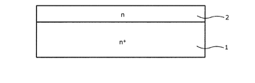
- FIG. 2 is a cross-sectional view showing a state in the middle of manufacture in the example of the method for manufacturing the semiconductor device according to the first embodiment of the present invention.
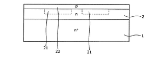
- FIG. 3 is a cross-sectional view showing a continuation of FIG.
- FIG. 4 is a cross-sectional view showing a continuation of FIG.
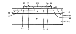
- FIG. 5 is a cross-sectional view showing a continuation of FIG. 6 is a cross-sectional view showing a continuation of FIG.
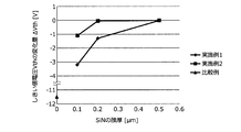
- FIG. 7 is a characteristic diagram showing an example of threshold voltage change characteristics between Examples 1 and 2 of the semiconductor device according to the first and second embodiments of the present invention and a comparative example.
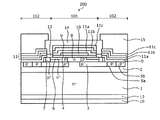
- FIG. 8 is a sectional view showing an example of a semiconductor device according to the second embodiment of the present invention.
- the semiconductor device is, for example, a 1200V withstand voltage class MOSFET
- the semiconductor device according to the present invention is not limited to a 1200V withstand voltage class MOSFET. Note that, in the following description of the embodiments and the accompanying drawings, the same reference numerals are given to the same components, and duplicate descriptions are omitted.
- FIG. 1 is a cross-sectional view showing an example of a semiconductor device according to the first embodiment of the present invention.
- the semiconductor device 100 according to the first embodiment includes an active region 101 and a breakdown voltage structure 102.
- the breakdown voltage structure 102 may be arranged so as to surround the active region 101.
- the semiconductor device 100 includes an n + semiconductor substrate 1 and an n semiconductor layer 2 made of silicon carbide.
- the n + semiconductor substrate 1 may be a silicon carbide single crystal substrate in which, for example, silicon carbide is doped with nitrogen atoms (N) at an impurity concentration of about 2 ⁇ 10 18 / cm 3 .
- the n + semiconductor substrate 1 becomes a drain region, for example.
- the first main surface of the n + semiconductor substrate 1 may be, for example, a (000-1) plane.
- the first main surface of the n + semiconductor substrate 1 may be, for example, a plane parallel to the (000-1) plane, or may be a plane inclined at an angle of 10 degrees or less.
- the first main surface of the n + semiconductor substrate 1 may be, for example, a (000-1) plane having an off angle of about 4 degrees in the ⁇ 11-20> direction.
- the front surface of the n + semiconductor substrate 1 is the first main surface and the back surface is the second main surface.
- the n semiconductor layer 2 is provided on the first main surface of the n + semiconductor substrate 1.
- the impurity concentration of the n semiconductor layer 2 is lower than that of the n + semiconductor substrate 1.
- the n semiconductor layer 2 may be a semiconductor layer in which, for example, silicon carbide is doped with nitrogen atoms at an impurity concentration of about 1 ⁇ 10 16 / cm 3 .
- the n semiconductor layer 2 becomes an n-type drift layer, for example.
- the thickness of the n semiconductor layer 2 may be about 10 ⁇ m, for example.
- the n semiconductor layer 2 may be stacked on the n + semiconductor substrate 1 by an epitaxial growth method.
- the MOS structure of the semiconductor device 100 that is, the element structure is formed on the first main surface side of the n + semiconductor substrate 1.
- the MOS structure of the semiconductor device 100 that is, the element structure is formed on the first main surface side of the n + semiconductor substrate 1.
- FIG. 1 only one MOS structure is shown in the active region 101, but a plurality of MOS structures may be provided in parallel.
- the semiconductor device 100 includes, for example, a p + semiconductor region 3, a p base region 4, an n + source region 6, a p + contact region 7, a source electrode 13, a gate insulating film 9, and a gate electrode 10 as a MOS structure.
- a back electrode to be the drain electrode 12 and a back electrode pad to be the drain electrode pad 16 are provided in the active region 101.
- the p + semiconductor region 3 is provided in a part of the surface region of the n semiconductor layer 2.
- the p + semiconductor region 3 may be provided, for example, so as to sandwich another part of the surface region of the n semiconductor layer 2.
- the p + semiconductor region 3 may be a semiconductor region in which, for example, silicon carbide is doped with aluminum atoms at an impurity concentration of about 3 ⁇ 10 18 / cm 3 .
- the width of the p + semiconductor region 3 may be about 13 ⁇ m, for example.
- the depth of the p + semiconductor region 3 may be about 0.5 ⁇ m, for example.
- a region between adjacent p + semiconductor regions 3 and p + semiconductor region 3 is a region of n semiconductor layer 2.
- the distance between adjacent p + semiconductor regions 3 and p + semiconductor regions 3 may be about 2 ⁇ m, for example.
- the p base region 4 is provided on the surface of the p + semiconductor region 3.
- the impurity concentration of the p base region 4 is lower than that of the p + semiconductor region 3.
- the p base region 4 may be a semiconductor region in which, for example, silicon carbide is doped with aluminum atoms at an impurity concentration of about 8 ⁇ 10 15 / cm 3 .
- the thickness of the p base region 4 may be about 0.5 ⁇ m, for example.
- the p base region 4 may be formed by patterning a p semiconductor layer stacked on the n semiconductor layer 2 by an epitaxial growth method.
- N well region 8 is provided on the surface of a region between adjacent p + semiconductor regions 3 and p + semiconductor region 3 of n semiconductor layer 2. N well region 8 is provided in contact with p base region 4. The impurity concentration of the n well region 8 is lower than that of the n + semiconductor substrate 1. The impurity concentration of the n-well region 8 may be about 2 ⁇ 10 16 / cm 3 , for example.
- the n-well region 8 is a region obtained by inverting the conductivity type of a part of the p-semiconductor layer stacked on the n-semiconductor layer 2 by, for example, epitaxial growth as described above by ion implantation of phosphorus atoms and heat treatment. Also good.
- n-well region 8 Some silicon atoms (Si) in the n-well region 8 are replaced with ion-implanted phosphorus atoms.
- the n-well region 8 becomes an n-type drift region together with the n semiconductor layer 2.
- the depth of the n well region 8 may be about 0.6 ⁇ m, for example.
- the width of the n-well region 8 may be about 2 ⁇ m, for example.
- n + source region 6 is provided in the surface region of the p base region 4 on the p + semiconductor region 3. N + source region 6 is provided apart from n well region 8. The impurity concentration of n + source region 6 is higher than that of n well region 8.
- the p + contact region 7 is provided on the opposite side of the n well region 8 across the p base region 4, that is, on the breakdown voltage structure portion 102 side away from the n well region 8.
- the p + contact region 7 is in contact with the n + source region 6.
- the p + contact region 7 penetrates the p semiconductor layer that becomes the p base region 4 on the n semiconductor layer 2 and is in contact with the p + semiconductor region 3.
- the impurity concentration of the p + contact region 7 is higher than that of the p base region 4.
- Gate insulating film 9 is provided on the surface of the region sandwiched between n well region 8 and n + source region 6 in p base region 4.
- the gate insulating film 9 extends from the surface of one p base region 4 adjacent to the n well region 8 to the surface of the other p base region 4 through the surface of the n well region 8, for example. Also good.
- the gate insulating film 9 may extend to the breakdown voltage structure 102.
- the gate insulating film 9 may be an oxide film, for example.
- the thickness of the gate insulating film 9 may be about 100 nm, for example.
- the gate electrode 10 is provided on the surface of the gate insulating film 9.
- the gate electrode 10 may extend, for example, from one adjacent p base region 4 across the n well region 8 to the other p base region 4 through the n well region 8.
- the gate electrode 10 may be made of a conductive material.
- the gate electrode 10 may be made of, for example, polycrystalline silicon doped with phosphorus atoms.
- the gate electrode 10 may be electrically connected to the gate pad in a region that does not appear in FIG.
- the gate electrode 10 is covered with an interlayer insulating film 11.
- the interlayer insulating film 11 extends to the breakdown voltage structure 102 and is provided on the entire surface on the side where the gate electrode 10 is provided.
- the interlayer insulating film 11 has a multilayer structure.
- the interlayer insulating film 11 may have a silicon oxide film 11a in a lower layer and a silicon nitride film 11b in an upper layer.
- the silicon oxide film 11a may be made of, for example, non-doped silicate glass (NSG: Nonsilicate Silicate Glass) or may be made of phosphorus glass (PSG: Phospho Silicate Glass).
- the thickness of the silicon oxide film 11a may be about 0.5 ⁇ m, for example.
- the thickness of the silicon nitride film 11b is preferably 3 ⁇ m or less, for example.
- the thickness of the silicon nitride film 11b may be, for example, about 0.5 ⁇ m.
- the source electrode 13 is provided, for example, in a contact hole that penetrates the interlayer insulating film 11 provided in the active region 101 and the breakdown voltage structure 102 and the gate insulating film 9 provided in the active region 101 and the breakdown voltage structure 102. Yes. Source electrode 13 is in contact with n + source region 6 and p + contact region 7. Source electrode 13 is electrically connected to n + source region 6 and p + contact region 7. The source electrode 13 is insulated from the gate electrode 10 by the interlayer insulating film 11.
- the semiconductor device 100 may have a source electrode pad 14.
- the source electrode pad 14 is provided so as to cover the source electrode 13 and the interlayer insulating film 11 in the active portion 101.
- the source electrode pad 14 is in contact with the source electrode 13.
- the source electrode pad 14 is electrically connected to the source electrode 13.
- the thickness of the portion of the source electrode pad 14 on the interlayer insulating film 11 may be 5 ⁇ m, for example.
- the source electrode pad 14 may be made of, for example, aluminum (Al).
- the drain electrode 12 is provided on the second main surface of the n + semiconductor substrate 1.
- the drain electrode 12 may be made of a conductive film, such as a metal film.
- the drain electrode 12 may be made of, for example, nickel (Ni).
- Ni nickel
- the drain electrode pad 16 is provided on the surface of the drain electrode 12.
- the drain electrode pad 16 may be made of a conductive film, for example, a metal film.
- the drain electrode pad 16 may be formed by, for example, sequentially laminating titanium (Ti), nickel, and gold (Au) from the drain electrode 12 side.
- the drain electrode pad 16 is electrically connected to the drain electrode 12.
- the semiconductor device 100 may include a p ⁇ semiconductor region 5 a, a p ⁇ semiconductor region 5 b, and a protective film 15 in the breakdown voltage structure 102.
- the p ⁇ semiconductor region 5 a is provided in a part of the surface region of the n semiconductor layer 2 in the breakdown voltage structure 102.
- the p ⁇ semiconductor region 5 a is in contact with, for example, the p + semiconductor region 3.
- the p ⁇ semiconductor region 5 a may be provided so as to surround the p + semiconductor region 3.
- the p ⁇ semiconductor region 5a may be a semiconductor region in which, for example, silicon carbide is doped with aluminum atoms.
- the impurity concentration of p ⁇ semiconductor region 5 a is lower than the impurity concentration of p + semiconductor region 3.
- the p 2 ⁇ semiconductor region 5 b is provided in part of the surface region of the n semiconductor layer 2 in the breakdown voltage structure 102.
- the p ⁇ semiconductor region 5b is in contact with, for example, the p ⁇ semiconductor region 5a.
- the p ⁇ semiconductor region 5b may be provided so as to surround the p ⁇ semiconductor region 5a.
- p - semiconductor regions 5b for example aluminum atoms may be a semiconductor region doped with silicon carbide.
- p - impurity concentration of the semiconductor region 5b is, p - lower than the impurity concentration of the semiconductor region 5a.
- the semiconductor device 100 includes a double zone JTE (junction) arranged in parallel so that two p-type regions having different impurity concentrations are in contact by the first p ⁇ -type region 5a and the second p ⁇ -type region 5b. It may have a Termination Extension) structure.
- the semiconductor device 100 is not limited to the double zone JTE structure, and may have a multi-zone JTE structure arranged in parallel so that three or more p-type regions having different impurity concentrations are in contact with each other. Further, the semiconductor device 100 may have a termination structure in which a plurality of p-type regions are arranged at a predetermined interval, such as a field limiting ring structure.
- the protective film 15 may be provided so as to cover the end of the source electrode pad 14 on the pressure-resistant structure 102 side.
- the protective film 15 becomes a passivation film.
- the protective film 15 has a function of preventing discharge.
- the protective film 15 may be made of polyimide, for example.
- FIG. 2 is a cross-sectional view showing a state in the middle of manufacturing in an example of a manufacturing method of the semiconductor device according to the first embodiment of the present invention.
- FIG. 3 is a cross-sectional view showing a continuation of FIG.
- FIG. 4 is a cross-sectional view showing a continuation of FIG.
- FIG. 5 is a cross-sectional view showing a continuation of FIG. 6 is a cross-sectional view showing a continuation of FIG.
- an n + semiconductor substrate 1 made of n-type silicon carbide is prepared.
- an n semiconductor layer 2 made of silicon carbide is epitaxially grown on the first main surface of the n + semiconductor substrate 1 to a thickness of, for example, about 10 ⁇ m while doping an n-type impurity such as a nitrogen atom.
- the state up to this point is shown in FIG.
- a mask (not shown) having a desired opening is formed on the surface of the n semiconductor layer 2 by photolithography.
- p-type impurities such as aluminum atoms are ion-implanted by ion implantation.
- a first ion implantation region 21 having a width of about 13 ⁇ m and a depth of about 0.5 ⁇ m is formed in a part of the surface region of the n semiconductor layer 2.
- the distance between the ion implantation region 21 and the first ion implantation region 21 is about 2 ⁇ m.
- the first ion implantation region 21 becomes the p + semiconductor region 3 through, for example, a heat treatment described later.
- the dose amount during ion implantation for providing the first ion implantation region 21 may be set so that the impurity concentration of the p + semiconductor region 3 is about 3 ⁇ 10 18 / cm 3 , for example.
- a second semiconductor layer 22 made of silicon carbide is epitaxially grown on the surface of the n semiconductor layer 2 to a thickness of, for example, about 0.5 ⁇ m while doping p-type impurities such as aluminum atoms.
- the second semiconductor layer 22 becomes the p base region 4 through, for example, a photolithography technique and an etching process which will be described later.
- the dose at the time of ion implantation for providing the second semiconductor layer 22 may be set so that the impurity concentration of the p base region 4 is about 8 ⁇ 10 15 / cm 3 , for example.
- the state up to here is shown in FIG.
- a mask (not shown) having a desired opening is formed on the surface of the second semiconductor layer 22 by photolithography.
- the p semiconductor region 22 is formed by patterning the second semiconductor layer 22 by performing an etching process, and the second semiconductor layer 22 is formed to have a thickness of, for example, about 0.7 ⁇ m in the region to be the breakdown voltage structure portion 102.
- the semiconductor layer 2 is exposed by removing at a depth.
- the mask used in the etching process for patterning the second semiconductor layer 22 is removed.
- a mask (not shown) having a desired opening is formed on the exposed surface of the n semiconductor layer 2 and the surface of the p base region 4 by photolithography.
- p-type impurities such as aluminum atoms are ion-implanted by ion implantation.
- the second ion implantation region 23 is formed in a part of the surface region of the n semiconductor layer 2, for example, in the first ion implantation region 21. It is provided to touch.
- the second ion implantation region 23 becomes, for example, the p ⁇ semiconductor region 5a in the above-described double zone JTE structure, for example, through a heat treatment described later.
- the dose amount at the time of ion implantation for providing the second ion implantation region 23 may be set to about 2 ⁇ 10 13 / cm 2 , for example. Subsequently, the mask used at the time of ion implantation for providing the second ion implantation region 23 is removed.
- a mask (not shown) having a desired opening is formed on the exposed surface of the n semiconductor layer 2 and the surface of the p base region 4 by photolithography.
- p-type impurities such as aluminum atoms are ion-implanted by ion implantation.
- the third ion implantation region 24 is formed in a part of the surface region of the n semiconductor layer 2, for example, in the second ion implantation region 23. It is provided to touch.
- the third ion implantation region 24 becomes, for example, the p ⁇ semiconductor region 5b in the above-described double zone JTE structure by performing a heat treatment described later, for example.
- the dose at the time of ion implantation for providing the third ion implantation region 24 may be set to, for example, about 1 ⁇ 10 13 / cm 2 .
- the mask used at the time of ion implantation for providing the third ion implantation region 24 is removed. The state up to this point is shown in FIG.
- a mask (not shown) having a desired opening is formed on the exposed surface of the n semiconductor layer 2 and the surface of the p base region 4 by photolithography.
- n-type impurities such as phosphorus atoms are ion-implanted by ion implantation.
- the region above the region of the n semiconductor layer 2 sandwiched between the adjacent first ion implantation region 21 and the first ion implantation region 21 is provided in this region.
- the fourth ion implantation region 25 becomes, for example, the n-well region 8 through, for example, heat treatment described later.
- the dose amount at the time of ion implantation for providing the fourth ion implantation region 25 may be set so that, for example, the impurity concentration of the n-well region 8 is about 2 ⁇ 10 16 / cm 3 .
- the mask used at the time of ion implantation for providing the fourth ion implantation region 25 is removed.
- a mask (not shown) having a desired opening is formed on the exposed surface of the n semiconductor layer 2 and the surface of the p base region 4 by photolithography. Then, n-type impurities are ion-implanted by ion implantation. Thereby, as indicated by a broken line in FIG. 5, a fifth ion implantation region 26 is provided in a region away from the fourth ion implantation region 25 in the surface region of the second semiconductor layer 22. The fifth ion implantation region 26 becomes, for example, the n + source region 6 through, for example, a heat treatment described later.
- the dose at the time of ion implantation for providing the fifth ion implantation region 26 may be set so that the impurity concentration is higher than that of the fourth ion implantation region 25. Subsequently, the mask used at the time of ion implantation for providing the fifth ion implantation region 26 is removed.
- a mask (not shown) having a desired opening is formed on the exposed surface of the n semiconductor layer 2 and the surface of the p base region 4 by photolithography.
- a p-type impurity is ion-implanted by an ion implantation method.
- a sixth ion implantation region 27 is provided in the second semiconductor layer 22 in the second semiconductor layer 22 in the second semiconductor layer 22, the region above the first ion implantation region 21 and the region in contact with the p base region 4 and the fifth ion implantation region 26.
- a sixth ion implantation region 27 is provided.
- the sixth ion implantation region 27 becomes, for example, the p + contact region 7 through, for example, a heat treatment described later.
- the dose at the time of ion implantation for providing the sixth ion implantation region 27 may be set so that the impurity concentration is higher than that of the p base region 4. Subsequently, the mask used at the time of ion implantation for providing the sixth ion implantation region 27 is removed.
- the order of ion implantation for providing the second ion implantation region 23, the third ion implantation region 24, the fourth ion implantation region 25, the fifth ion implantation region 26, and the sixth ion implantation region 27, respectively. are not limited to the order described above, and can be variously changed. The state up to here is shown in FIG.
- heat treatment for example, a first ion implantation region 21, a second ion implantation region 23, a third ion implantation region 24, a fourth ion implantation region 25,
- the fifth ion implantation region 26 and the sixth ion implantation region 27 are activated.
- the first ion implantation region 21 becomes the p + semiconductor region 3.
- the fourth ion-implanted region 25 becomes the n-well region 8 by replacing the ion-implanted phosphorus atoms with silicon atoms and inverting the conductivity type.
- the fifth ion implantation region 26 becomes the n + source region 6.
- the sixth ion implantation region 27 becomes the p + contact region 7.
- Second ion implantation region 23 becomes p ⁇ semiconductor region 5a.
- the third ion implantation region 24 becomes the p ⁇ semiconductor region 5b.
- the temperature of the heat treatment may be about 1620 ° C., for example.
- the heat treatment time may be, for example, about 2 minutes.
- the respective ion implantation regions may be activated collectively by one heat treatment, or may be activated by performing heat treatment every time ion implantation is performed.
- the surface on which the p base region 4, the n + source region 6, the p + contact region 7, the n well region 8, the p ⁇ semiconductor region 5a and the p ⁇ semiconductor region 5b are provided is thermally oxidized, for example,
- a gate insulating film 9 having a thickness of about 100 nm is provided on the entire surface.
- This thermal oxidation treatment may be realized, for example, by performing a heat treatment at a temperature of, for example, about 1000 ° C. in an oxygen atmosphere.
- a polycrystalline silicon layer doped with, for example, phosphorus atoms is provided on the gate insulating film 9.
- the polycrystalline silicon layer is patterned and left on the gate insulating film 9 on the region of the p base region 4 sandwiched between the n + source region 6 and the n well region 8, thereby providing the gate electrode 10. .
- non-doped silicate glass (NSG) or phosphorus glass (PSG) is formed to a thickness of, for example, about 0.5 ⁇ m so as to cover the gate insulating film 9 and the gate electrode 10.
- a silicon oxide film 11a is provided.
- silicon nitride is formed to a thickness of, for example, about 0.5 ⁇ m so as to cover the silicon oxide film 11 a, and a silicon nitride film 11 b that is an upper layer of the interlayer insulating film 11 is provided.
- the interlayer insulating film 11 is completed by the silicon oxide film 11a and the silicon nitride film 11b.
- the silicon nitride film 11b may be formed by plasma CVD (Chemical Vapor Deposition). The state up to this point is shown in FIG.
- the silicon nitride film 11b, the silicon oxide film 11a and the gate insulating film 9 are selectively removed by patterning to form contact holes, and n + source regions 6 and p + contacts. Region 7 is exposed. Thereafter, heat treatment (reflow) is performed to planarize the interlayer insulating film 11.
- a conductive film to be the source electrode 13 is provided in the contact hole and on the interlayer insulating film 11.
- the conductive film is selectively removed to leave the source electrode 13 only in the contact hole, for example.
- the drain electrode 12 made of, for example, a nickel film is provided on the second main surface of the n + semiconductor substrate 1. Thereafter, heat treatment is performed at a temperature of, for example, about 970 ° C., and the n + semiconductor substrate 1 and the drain electrode 12 are ohmic-bonded.
- an aluminum (Al) film for example, is provided so as to cover the source electrode 13 and the interlayer insulating film 11 so that the thickness of the upper part of the interlayer insulating film 11 becomes, for example, about 5 ⁇ m. . Thereafter, the Al film is selectively removed to leave the source electrode 13 and the interlayer insulating film 11 in the active region 101 so as to form the source electrode pad 14.
- the drain electrode pad 16 is provided on the surface of the drain electrode 12 by sequentially laminating, for example, titanium, nickel, and gold. As described above, the semiconductor device 100 shown in FIG. 1 is completed.
- Example 1 A semiconductor device 100 in which an interlayer insulating film 11 is composed of a lower silicon oxide film 11a and an upper silicon nitride film 11b is referred to as a first embodiment.
- a semiconductor device in which the interlayer insulating film 11 is made of only a silicon oxide film is used as a comparative example.
- FIG. 7 is a characteristic diagram showing an example of threshold voltage change characteristics between Examples 1 and 2 of the semiconductor device according to the first and second embodiments of the present invention and a comparative example.
- the vertical axis represents the change amount ⁇ Vth (unit: V) of the threshold voltage Vth
- the horizontal axis represents the film thickness (unit: ⁇ m) of the silicon nitride film.
- the thickness of the silicon nitride film is zero.
- ⁇ Vth was ⁇ 11 V or more in the comparative example, but it was confirmed that in Example 1, ⁇ Vth was improved compared to the comparative example. It was also confirmed that ⁇ Vth was improved to ⁇ 0.1 V or less by setting the thickness of the silicon nitride film 11 b to 0.5 ⁇ m or more.
- the presence of a layer made of the silicon nitride film 11b in the interlayer insulating film 11 causes an element that causes a decrease in threshold voltage at the interface between the silicon oxide film and the semiconductor. Since diffusion is prevented, a decrease in threshold voltage is suppressed. Thereby, it is possible to suppress the deterioration of the characteristics of the semiconductor device 100. Further, according to the first embodiment, it is possible to avoid a decrease in reliability due to a reliability test such as a high temperature gate bias (HTGB) test. Further, according to the first embodiment, since the silicon oxide film 11a having better coverage than the silicon nitride film 11b exists in the layer below the silicon nitride film 11b, the coverage of the interlayer insulating film 11 is improved.
- HTGB high temperature gate bias
- the occurrence of problems such as cracks can be avoided. Therefore, it is possible to improve the amount of change in threshold voltage while fulfilling the function as an interlayer insulating film having a MOS structure. Further, according to the first embodiment, since a titanium-based barrier metal is unnecessary, it is not necessary to perform etching of a titanium-based metal separately from the etching of the source electrode pad 14, and the number of processes during manufacturing is increased. Can be suppressed.
- FIG. 8 is a cross-sectional view showing an example of a semiconductor device according to the second embodiment of the present invention.
- the semiconductor device 200 according to the second embodiment includes, as an interlayer insulating film 11, a silicon oxide film 11a as a lower layer, a silicon nitride film 11b as an intermediate layer, and a second layer as an uppermost layer.
- the silicon oxide film 11c is provided.
- the interlayer insulating film 11 may have a structure of four layers or more, the second embodiment will be described as having a three-layer structure.
- the second silicon oxide film 11c may be made of non-doped silicate glass (NSG), for example, or may be made of phosphorus glass (PSG).
- the second silicon oxide film 11c may be made of, for example, glass in which boron and phosphorus are added to silicon oxide (BPSG: Boro-Phospho Silicate Glass). If the second silicon oxide film 11c is made of BPSG, there is an effect that the optimum flattening by reflow can be realized.
- a gate electrode 10 is provided in the same manner as the manufacturing method of the semiconductor device 100 according to the first embodiment, and a silicon oxide film 11a that is a lower layer in the interlayer insulating film 11 and an intermediate layer After providing the silicon nitride film 11b to be a layer, the second silicon oxide film 11c to be the uppermost layer is provided. Thereby, the interlayer insulating film 11 is formed by the silicon oxide film 11a, the silicon nitride film 11b, and the second silicon oxide film 11c.
- the second silicon oxide film 11c, the silicon nitride film 11b, the silicon oxide film 11a and the gate insulating film 9 are selectively removed by patterning to form contact holes, and n + source regions 6 and p + The contact region 7 is exposed. Thereafter, heat treatment (reflow) is performed to planarize the interlayer insulating film 11. Subsequent processes are the same as those of the method for manufacturing the semiconductor device 100 according to the first embodiment, and thus redundant description is omitted.
- Example 2 A semiconductor device 200 in which the interlayer insulating film 11 is composed of a lower silicon oxide film 11a, an intermediate silicon nitride film 11b, and an uppermost second silicon oxide film 11c is referred to as a second embodiment.
- a semiconductor device in which the interlayer insulating film 11 is made of only a silicon oxide film is used as a comparative example.
- the comparative example in the second embodiment is the same as the comparative example in the first embodiment.
- Example 2 the amount of change ( ⁇ Vth) in threshold voltage (Vth) was evaluated.
- ⁇ Vth the difference between the initial threshold voltage value and the threshold voltage value after applying a voltage of ⁇ 20 V between the gate and the source at 200 ° C. for 10 minutes was defined as ⁇ Vth.
- the result of evaluating ⁇ Vth will be described. As shown in FIG. 7, as a result of the evaluation, it was confirmed that in Example 2, ⁇ Vth was improved as compared with the comparative example. Further, it was confirmed that ⁇ Vth was improved to ⁇ 0.1 V or less by setting the thickness of the silicon nitride film 11 b to 0.2 ⁇ m or more.
- the semiconductor device 200 since there is a layer made of the silicon nitride film 11b in the interlayer insulating film 11, a decrease in threshold voltage is suppressed, so that the semiconductor device 200 It is possible to suppress the deterioration of the characteristics. Further, according to the second embodiment, as in the first embodiment, it is possible to avoid a decrease in reliability due to the reliability test. In addition, according to the second embodiment, as in the first embodiment, since there is a layer made of the silicon oxide film 11a in the interlayer insulating film 11, the function as the interlayer insulating film of the MOS structure is achieved. The amount of change in threshold voltage can be improved. Further, according to the second embodiment, as in the first embodiment, since a titanium-based barrier metal is not necessary, an increase in the number of processes during manufacturing can be suppressed.
- the surface orientation of the first main surface of the n + semiconductor substrate 1 can be variously changed.
- the first main surface of the n + semiconductor substrate 1 is a plane parallel to the (0001) plane, or a plane inclined at an angle of 10 degrees or less with respect to the (0001) plane, for example, 4 in the ⁇ 11-20> direction. It may be a (0001) plane having an off angle on the order of degrees.
- the dimensions and concentrations described in each embodiment are examples, and the present invention is not limited to these values.
- the first conductivity type is n-type and the second conductivity type is p-type.
- the first conductivity type is p-type and the second conductivity type is n-type. It holds.
- the semiconductor device according to the present invention is useful for a high voltage semiconductor device, for example, and is particularly suitable for a high voltage semiconductor device used for a power supply device such as a power converter and various industrial machines. ing.
Landscapes
- Electrodes Of Semiconductors (AREA)
Abstract
Description
・実施の形態1にかかる半導体装置の一例
図1は、本発明の実施の形態1にかかる半導体装置の一例を示す断面図である。図1に示すように、実施の形態1にかかる半導体装置100は、活性領域101及び耐圧構造部102を有する。耐圧構造部102は、活性領域101を囲むように配置されていてもよい。半導体装置100は、炭化珪素でできたn+半導体基板1及びn半導体層2を備えている。
図2は、本発明の実施の形態1にかかる半導体装置の製造方法の一例における製造途中の状態を示す断面図である。図3は、図2の続きの状態を示す断面図である。図4は、図3の続きの状態を示す断面図である。図5は、図4の続きの状態を示す断面図である。図6は、図5の続きの状態を示す断面図である。
層間絶縁膜11が下層の酸化珪素膜11aと上層の窒化珪素膜11bとでできている半導体装置100を実施例1とする。半導体装置100において、層間絶縁膜11が酸化珪素膜のみでできている半導体装置を比較例とする。
・実施の形態2にかかる半導体装置の一例
図8は、本発明の実施の形態2にかかる半導体装置の一例を示す断面図である。図8に示すように、実施の形態2にかかる半導体装置200は、層間絶縁膜11として、下層に酸化珪素膜11aを有し、中間層に窒化珪素膜11bを有し、最上層に第2の酸化珪素膜11cを有するものである。なお、層間絶縁膜11は、4層以上の構造であってもよいが、実施の形態2では、3層構造であるとして説明する。
実施の形態1にかかる半導体装置100の製造方法と同様にしてゲート電極10を設け、層間絶縁膜11において下層となる酸化珪素膜11a及び中間層となる窒化珪素膜11bを設けた後、最上層となる第2の酸化珪素膜11cを設ける。それによって、酸化珪素膜11a、窒化珪素膜11b及び第2の酸化珪素膜11cによって層間絶縁膜11ができあがる。
層間絶縁膜11が下層の酸化珪素膜11aと中間層の窒化珪素膜11bと最上層の第2の酸化珪素膜11cとでできている半導体装置200を実施例2とする。半導体装置200において、層間絶縁膜11が酸化珪素膜のみでできている半導体装置を比較例とする。実施の形態2における比較例は、実施の形態1における比較例と同じものである。
2 n半導体層
3 p+半導体領域
4 pベース領域
5a p-半導体領域
5b p--半導体領域
6 n+ソース領域
7 p+コンタクト領域
8 nウェル領域
9 ゲート絶縁膜
10 ゲート電極
11 層間絶縁膜
11a 酸化珪素膜
11b 窒化珪素膜
11c 第2の酸化珪素膜
12 ドレイン電極
13 ソース電極
14 ソース電極パッド
15 保護膜
16 ドレイン電極パッド
21 第1のイオン注入領域
22 第2の半導体層
23 第2のイオン注入領域
24 第3のイオン注入領域
25 第4のイオン注入領域
26 第5のイオン注入領域
27 第6のイオン注入領域
100,200 半導体装置
Claims (11)
- 第1導電型の炭化珪素でできた半導体基板と、
前記半導体基板の第1主面上に設けられた、前記半導体基板よりも不純物濃度の低い第1導電型の半導体層と、
前記半導体層の表面上に設けられた第2導電型のベース領域と、
前記ベース領域の表面領域に設けられた第1導電型のソース領域と、
前記ベース領域の表面領域に設けられた、前記ベース領域よりも不純物濃度の高い第2導電型のコンタクト領域と、
前記ソース領域及び前記コンタクト領域に接するソース電極と、
前記ベース領域の、前記半導体層と前記ソース領域とに挟まれた領域の表面上に設けられたゲート絶縁膜と、
前記ゲート絶縁膜の表面上に設けられたゲート電極と、
前記ゲート電極の表面上に設けられた層間絶縁膜と、
前記半導体基板の第2主面上に設けられたドレイン電極と、を備え、
前記層間絶縁膜が複数の層を有し、かつ前記複数の層のうちの少なくとも1層が窒化珪素膜でできていることを特徴とする半導体装置。 - 第1導電型の炭化珪素でできた半導体基板と、
前記半導体基板の第1主面上に設けられた、前記半導体基板よりも不純物濃度の低い第1導電型の半導体層と、
前記半導体層の表面領域の一部に設けられた第2導電型の半導体領域と、
前記半導体領域の表面上に設けられた、前記半導体領域よりも不純物濃度の低い第2導電型のベース領域と、
前記半導体層の表面上に前記ベース領域に接して設けられた、前記半導体基板よりも不純物濃度の低い第1導電型の炭化珪素でできたウェル領域と、
前記ベース領域の表面領域に前記ウェル領域から離れて設けられた、前記ウェル領域よりも不純物濃度の高い第1導電型のソース領域と、
前記ベース領域の表面上に前記ソース領域に接して設けられた、前記ベース領域よりも不純物濃度の高い第2導電型のコンタクト領域と、
前記ソース領域及び前記コンタクト領域に接するソース電極と、
前記ベース領域の、前記ウェル領域と前記ソース領域とに挟まれた領域の表面上に設けられたゲート絶縁膜と、
前記ゲート絶縁膜の表面上に設けられたゲート電極と、
前記ゲート電極の表面上に設けられた層間絶縁膜と、
前記半導体基板の第2主面上に設けられたドレイン電極と、を備え、
前記層間絶縁膜が複数の層を有し、かつ前記複数の層のうちの少なくとも1層が窒化珪素膜でできていることを特徴とする半導体装置。 - 前記層間絶縁膜において前記窒化珪素膜でできた層は、酸化珪素膜でできた層で挟まれていることを特徴とする請求項1または2に記載の半導体装置。
- 前記層間絶縁膜において前記窒化珪素膜でできた層の厚さは、0.2μm以上であることを特徴とする請求項3に記載の半導体装置。
- 前記層間絶縁膜において前記窒化珪素膜でできた層の上の前記酸化珪素膜でできた層は、酸化珪素中にボロン及びリンが添加されたガラスでできていることを特徴とする請求項4に記載の半導体装置。
- 前記層間絶縁膜において前記窒化珪素膜でできた層は、最も上の層であることを特徴とする請求項1または2に記載の半導体装置。
- 前記層間絶縁膜において前記窒化珪素膜でできた層の厚さは、0.5μm以上であることを特徴とする請求項6に記載の半導体装置。
- 前記半導体基板の前記第1主面の結晶学的面指数は、(000-1)面に対して、平行な面または10度以内に傾いた面であることを特徴とする請求項1または2に記載の半導体装置。
- 前記半導体基板の前記第1主面の結晶学的面指数は、(0001)面に対して、平行な面または10度以内に傾いた面であることを特徴とする請求項1または2に記載の半導体装置。
- 第1導電型の炭化珪素でできた半導体基板と、前記半導体基板の第1主面上に設けられた、前記半導体基板よりも不純物濃度の低い第1導電型の半導体層と、前記半導体層の表面上に設けられた第2導電型のベース領域と、前記ベース領域の表面領域に設けられた第1導電型のソース領域と、前記ベース領域の表面領域に設けられた、前記ベース領域よりも不純物濃度の高い第2導電型のコンタクト領域と、前記ソース領域及び前記コンタクト領域に接するソース電極と、前記ベース領域の、前記半導体層と前記ソース領域とに挟まれた領域の表面上に設けられたゲート絶縁膜と、前記ゲート絶縁膜の表面上に設けられたゲート電極と、前記ゲート電極の表面上に設けられた層間絶縁膜と、前記半導体基板の第2主面上に設けられたドレイン電極と、を備えた半導体装置の製造方法において、
前記層間絶縁膜を複数の層で形成し、かつ前記複数の層のうちの少なくとも1層を窒化珪素膜で形成したことを特徴とする半導体装置の製造方法。 - 第1導電型の炭化珪素でできた半導体基板と、前記半導体基板の第1主面上に設けられた、前記半導体基板よりも不純物濃度の低い第1導電型の半導体層と、前記半導体層の表面領域の一部に設けられた第2導電型の半導体領域と、前記半導体領域の表面上に設けられた、前記半導体領域よりも不純物濃度の低い第2導電型のベース領域と、前記半導体層の表面上に前記ベース領域に接して設けられた、前記半導体基板よりも不純物濃度の低い第1導電型の炭化珪素でできたウェル領域と、前記ベース領域の表面領域に前記ウェル領域から離れて設けられた、前記ウェル領域よりも不純物濃度の高い第1導電型のソース領域と、前記ベース領域の表面上に前記ソース領域に接して設けられた、前記ベース領域よりも不純物濃度の高い第2導電型のコンタクト領域と、前記ソース領域及び前記コンタクト領域に接するソース電極と、前記ベース領域の、前記ウェル領域と前記ソース領域とに挟まれた領域の表面上に設けられたゲート絶縁膜と、前記ゲート絶縁膜の表面上に設けられたゲート電極と、前記ゲート電極の表面上に設けられた層間絶縁膜と、前記半導体基板の第2主面上に設けられたドレイン電極と、を備えた半導体装置の製造方法において、
前記層間絶縁膜を複数の層で形成し、かつ前記複数の層のうちの少なくとも1層を窒化珪素膜で形成したことを特徴とする半導体装置の製造方法。
Priority Applications (4)
| Application Number | Priority Date | Filing Date | Title |
|---|---|---|---|
| JP2016535898A JP6197957B2 (ja) | 2014-07-23 | 2015-07-15 | 半導体装置及び半導体装置の製造方法 |
| CN201580003426.5A CN105849877B (zh) | 2014-07-23 | 2015-07-15 | 半导体装置以及半导体装置的制造方法 |
| DE112015000244.8T DE112015000244T5 (de) | 2014-07-23 | 2015-07-15 | Halbleitervorrichtung und Verfahren zum Herstellen einer Halbleitervorrichtung |
| US15/201,211 US10079298B2 (en) | 2014-07-23 | 2016-07-01 | Semiconductor device and method of manufacturing semiconductor device |
Applications Claiming Priority (2)
| Application Number | Priority Date | Filing Date | Title |
|---|---|---|---|
| JP2014150256 | 2014-07-23 | ||
| JP2014-150256 | 2014-07-23 |
Related Child Applications (1)
| Application Number | Title | Priority Date | Filing Date |
|---|---|---|---|
| US15/201,211 Continuation US10079298B2 (en) | 2014-07-23 | 2016-07-01 | Semiconductor device and method of manufacturing semiconductor device |
Publications (1)
| Publication Number | Publication Date |
|---|---|
| WO2016013471A1 true WO2016013471A1 (ja) | 2016-01-28 |
Family
ID=55162997
Family Applications (1)
| Application Number | Title | Priority Date | Filing Date |
|---|---|---|---|
| PCT/JP2015/070336 Ceased WO2016013471A1 (ja) | 2014-07-23 | 2015-07-15 | 半導体装置及び半導体装置の製造方法 |
Country Status (5)
| Country | Link |
|---|---|
| US (1) | US10079298B2 (ja) |
| JP (1) | JP6197957B2 (ja) |
| CN (1) | CN105849877B (ja) |
| DE (1) | DE112015000244T5 (ja) |
| WO (1) | WO2016013471A1 (ja) |
Cited By (2)
| Publication number | Priority date | Publication date | Assignee | Title |
|---|---|---|---|---|
| JP2017168677A (ja) * | 2016-03-16 | 2017-09-21 | 富士電機株式会社 | 炭化珪素半導体装置および炭化珪素半導体装置の製造方法 |
| WO2018135146A1 (ja) * | 2017-01-17 | 2018-07-26 | 富士電機株式会社 | 半導体装置および半導体装置の製造方法 |
Families Citing this family (5)
| Publication number | Priority date | Publication date | Assignee | Title |
|---|---|---|---|---|
| JP6853621B2 (ja) * | 2016-03-17 | 2021-03-31 | 国立大学法人大阪大学 | 炭化珪素半導体装置の製造方法 |
| JP6862381B2 (ja) * | 2018-03-02 | 2021-04-21 | 株式会社東芝 | 半導体装置 |
| JP7242488B2 (ja) * | 2019-09-17 | 2023-03-20 | 株式会社東芝 | 半導体装置の製造方法 |
| JP7487094B2 (ja) * | 2020-12-23 | 2024-05-20 | 株式会社 日立パワーデバイス | 半導体装置 |
| CN116613215B (zh) * | 2023-06-26 | 2024-07-19 | 陕西亚成微电子股份有限公司 | 一种线性平面功率vdmos结构及其制备方法 |
Citations (4)
| Publication number | Priority date | Publication date | Assignee | Title |
|---|---|---|---|---|
| JP2000012856A (ja) * | 1998-06-26 | 2000-01-14 | Sony Corp | Mosトランジスタの製造方法 |
| JP2002184987A (ja) * | 2000-12-15 | 2002-06-28 | Nec Kansai Ltd | 半導体装置 |
| WO2004036655A1 (ja) * | 2002-10-18 | 2004-04-29 | National Institute Of Advanced Industrial Science And Technology | 炭化ケイ素半導体装置及びその製造方法 |
| JP2008098593A (ja) * | 2006-09-15 | 2008-04-24 | Ricoh Co Ltd | 半導体装置及びその製造方法 |
Family Cites Families (6)
| Publication number | Priority date | Publication date | Assignee | Title |
|---|---|---|---|---|
| JPH11251592A (ja) * | 1998-01-05 | 1999-09-17 | Denso Corp | 炭化珪素半導体装置 |
| US6686616B1 (en) * | 2000-05-10 | 2004-02-03 | Cree, Inc. | Silicon carbide metal-semiconductor field effect transistors |
| JP2002076336A (ja) * | 2000-09-01 | 2002-03-15 | Mitsubishi Electric Corp | 半導体装置およびsoi基板 |
| JP4304332B2 (ja) * | 2003-10-03 | 2009-07-29 | 独立行政法人産業技術総合研究所 | 炭化ケイ素半導体装置 |
| JP5098294B2 (ja) * | 2006-10-30 | 2012-12-12 | 株式会社デンソー | 炭化珪素半導体装置の製造方法 |
| JP5694119B2 (ja) | 2010-11-25 | 2015-04-01 | 三菱電機株式会社 | 炭化珪素半導体装置 |
-
2015
- 2015-07-15 WO PCT/JP2015/070336 patent/WO2016013471A1/ja not_active Ceased
- 2015-07-15 DE DE112015000244.8T patent/DE112015000244T5/de not_active Withdrawn
- 2015-07-15 CN CN201580003426.5A patent/CN105849877B/zh active Active
- 2015-07-15 JP JP2016535898A patent/JP6197957B2/ja active Active
-
2016
- 2016-07-01 US US15/201,211 patent/US10079298B2/en active Active
Patent Citations (4)
| Publication number | Priority date | Publication date | Assignee | Title |
|---|---|---|---|---|
| JP2000012856A (ja) * | 1998-06-26 | 2000-01-14 | Sony Corp | Mosトランジスタの製造方法 |
| JP2002184987A (ja) * | 2000-12-15 | 2002-06-28 | Nec Kansai Ltd | 半導体装置 |
| WO2004036655A1 (ja) * | 2002-10-18 | 2004-04-29 | National Institute Of Advanced Industrial Science And Technology | 炭化ケイ素半導体装置及びその製造方法 |
| JP2008098593A (ja) * | 2006-09-15 | 2008-04-24 | Ricoh Co Ltd | 半導体装置及びその製造方法 |
Cited By (5)
| Publication number | Priority date | Publication date | Assignee | Title |
|---|---|---|---|---|
| JP2017168677A (ja) * | 2016-03-16 | 2017-09-21 | 富士電機株式会社 | 炭化珪素半導体装置および炭化珪素半導体装置の製造方法 |
| US10573716B2 (en) | 2016-03-16 | 2020-02-25 | Fuji Electric Co., Ltd. | Method of manufacturing a silicon carbide semiconductor device including depositing a second silicon carbide semiconductor on an etched silicon carbide base region |
| WO2018135146A1 (ja) * | 2017-01-17 | 2018-07-26 | 富士電機株式会社 | 半導体装置および半導体装置の製造方法 |
| JPWO2018135146A1 (ja) * | 2017-01-17 | 2019-06-27 | 富士電機株式会社 | 半導体装置および半導体装置の製造方法 |
| US10868168B2 (en) | 2017-01-17 | 2020-12-15 | Fuji Electric Co., Ltd. | Semiconductor device and method of manufacturing semiconductor device |
Also Published As
| Publication number | Publication date |
|---|---|
| JP6197957B2 (ja) | 2017-09-20 |
| CN105849877B (zh) | 2019-06-25 |
| CN105849877A (zh) | 2016-08-10 |
| JPWO2016013471A1 (ja) | 2017-04-27 |
| US20160315186A1 (en) | 2016-10-27 |
| DE112015000244T5 (de) | 2016-09-08 |
| US10079298B2 (en) | 2018-09-18 |
Similar Documents
| Publication | Publication Date | Title |
|---|---|---|
| JP6197957B2 (ja) | 半導体装置及び半導体装置の製造方法 | |
| JP6572423B2 (ja) | 半導体装置および半導体装置の製造方法 | |
| JP6086360B2 (ja) | 炭化珪素半導体装置の製造方法 | |
| CN104064587B (zh) | 半导体装置及其制造方法 | |
| US9613809B2 (en) | Method of manufacturing silicon carbide semiconductor device | |
| CN104064588A (zh) | 半导体装置及其制造方法 | |
| JP2012190982A (ja) | 半導体装置とその製造方法 | |
| CN105493245A (zh) | 碳化硅半导体元件以及碳化硅半导体元件的制造方法 | |
| JP6208106B2 (ja) | 半導体装置及びその製造方法 | |
| JPWO2016013472A1 (ja) | 半導体装置および半導体装置の製造方法 | |
| JP6500912B2 (ja) | 炭化珪素半導体装置および炭化珪素半導体装置の製造方法 | |
| JP6582537B2 (ja) | 半導体装置および半導体装置の製造方法 | |
| JP2025007330A (ja) | 炭化珪素半導体装置の製造方法および炭化珪素半導体装置 | |
| JP6589263B2 (ja) | 半導体装置 | |
| JP2018082054A (ja) | 炭化珪素半導体装置の製造方法、および炭化珪素半導体装置 | |
| WO2013046943A1 (ja) | 窒化物半導体装置およびその製造方法 | |
| JP6690333B2 (ja) | 炭化珪素半導体装置および炭化珪素半導体装置の製造方法 | |
| WO2019198167A1 (ja) | 半導体装置の製造方法及び半導体装置 | |
| JP6441412B2 (ja) | 半導体装置 | |
| JP2016058661A (ja) | 半導体装置 | |
| JP2013222800A (ja) | 窒化物半導体装置およびその製造方法 | |
| JP6277902B2 (ja) | 半導体装置及び半導体装置の製造方法 | |
| JP6233537B2 (ja) | 半導体装置および半導体装置の製造方法 | |
| JP6183234B2 (ja) | 半導体装置および半導体装置の製造方法 | |
| JP5329606B2 (ja) | 窒化物半導体装置の製造方法 |
Legal Events
| Date | Code | Title | Description |
|---|---|---|---|
| 121 | Ep: the epo has been informed by wipo that ep was designated in this application |
Ref document number: 15824902 Country of ref document: EP Kind code of ref document: A1 |
|
| ENP | Entry into the national phase |
Ref document number: 2016535898 Country of ref document: JP Kind code of ref document: A |
|
| WWE | Wipo information: entry into national phase |
Ref document number: 112015000244 Country of ref document: DE |
|
| 122 | Ep: pct application non-entry in european phase |
Ref document number: 15824902 Country of ref document: EP Kind code of ref document: A1 |